US6993692B2 - Method, system and apparatus for aggregating failures across multiple memories and applying a common defect repair solution to all of the multiple memories - Google Patents
Method, system and apparatus for aggregating failures across multiple memories and applying a common defect repair solution to all of the multiple memoriesDownload PDFInfo
- Publication number
- US6993692B2 US6993692B2US10/604,195US60419503AUS6993692B2US 6993692 B2US6993692 B2US 6993692B2US 60419503 AUS60419503 AUS 60419503AUS 6993692 B2US6993692 B2US 6993692B2
- Authority
- US
- United States
- Prior art keywords
- memory arrays
- failing
- address
- storage location
- integrated circuit
- Prior art date
- Legal status (The legal status is an assumption and is not a legal conclusion. Google has not performed a legal analysis and makes no representation as to the accuracy of the status listed.)
- Expired - Lifetime, expires
Links
Images


Classifications
- G—PHYSICS
- G11—INFORMATION STORAGE
- G11C—STATIC STORES
- G11C29/00—Checking stores for correct operation ; Subsequent repair; Testing stores during standby or offline operation
- G11C29/04—Detection or location of defective memory elements, e.g. cell constructio details, timing of test signals
- G11C29/08—Functional testing, e.g. testing during refresh, power-on self testing [POST] or distributed testing
- G11C29/12—Built-in arrangements for testing, e.g. built-in self testing [BIST] or interconnection details
- G11C29/44—Indication or identification of errors, e.g. for repair
- G11C29/4401—Indication or identification of errors, e.g. for repair for self repair
- G—PHYSICS
- G11—INFORMATION STORAGE
- G11C—STATIC STORES
- G11C29/00—Checking stores for correct operation ; Subsequent repair; Testing stores during standby or offline operation
- G11C29/04—Detection or location of defective memory elements, e.g. cell constructio details, timing of test signals
- G11C29/08—Functional testing, e.g. testing during refresh, power-on self testing [POST] or distributed testing
- G11C29/12—Built-in arrangements for testing, e.g. built-in self testing [BIST] or interconnection details
- G11C29/44—Indication or identification of errors, e.g. for repair
- G—PHYSICS
- G11—INFORMATION STORAGE
- G11C—STATIC STORES
- G11C29/00—Checking stores for correct operation ; Subsequent repair; Testing stores during standby or offline operation
- G11C29/70—Masking faults in memories by using spares or by reconfiguring
- G11C29/78—Masking faults in memories by using spares or by reconfiguring using programmable devices
- G11C29/80—Masking faults in memories by using spares or by reconfiguring using programmable devices with improved layout
- G11C29/802—Masking faults in memories by using spares or by reconfiguring using programmable devices with improved layout by encoding redundancy signals
- G—PHYSICS
- G11—INFORMATION STORAGE
- G11C—STATIC STORES
- G11C29/00—Checking stores for correct operation ; Subsequent repair; Testing stores during standby or offline operation
- G11C29/70—Masking faults in memories by using spares or by reconfiguring
- G11C29/78—Masking faults in memories by using spares or by reconfiguring using programmable devices
- G11C29/80—Masking faults in memories by using spares or by reconfiguring using programmable devices with improved layout
- G11C29/806—Masking faults in memories by using spares or by reconfiguring using programmable devices with improved layout by reducing size of decoders
- G—PHYSICS
- G11—INFORMATION STORAGE
- G11C—STATIC STORES
- G11C29/00—Checking stores for correct operation ; Subsequent repair; Testing stores during standby or offline operation
- G11C29/04—Detection or location of defective memory elements, e.g. cell constructio details, timing of test signals
- G11C2029/0401—Detection or location of defective memory elements, e.g. cell constructio details, timing of test signals in embedded memories
- G—PHYSICS
- G11—INFORMATION STORAGE
- G11C—STATIC STORES
- G11C29/00—Checking stores for correct operation ; Subsequent repair; Testing stores during standby or offline operation
- G11C29/70—Masking faults in memories by using spares or by reconfiguring
- G11C29/78—Masking faults in memories by using spares or by reconfiguring using programmable devices
- G11C29/785—Masking faults in memories by using spares or by reconfiguring using programmable devices with redundancy programming schemes
- G11C29/789—Masking faults in memories by using spares or by reconfiguring using programmable devices with redundancy programming schemes using non-volatile cells or latches
Definitions
- the present inventionrelates in general to integrated circuitry and, in particular, to integrated circuits including multiple memory arrays. Still more particularly, the present invention relates to the aggregation of detected failures across multiple memory arrays and the application of a common repair solution to all of the multiple memory arrays.
- ICstypically have far fewer I/O pins available to an external circuit tester than are required to adequately test the memory array.
- BISTbuilt-in self-test
- ASTarray self-test
- ABISTarray built-in self-test
- BIST circuitsAlthough the integration of BIST circuits within ICs facilitates IC testing, a central concern associated with BIST circuits is the large amount of die size consumed by the BIST circuit and associated circuitry. This concern is magnified as the number of memory arrays and other subcircuits integrated within an IC that require BIST testing multiply. This concern is particularly significant for state-of-the-art integrated circuits, such as a microprocessors and Application-Specific Integrated Circuits (ASICs), which commonly contain hundreds or thousands of relatively small memory arrays each requiring BIST testing.
- ASICsApplication-Specific Integrated Circuits
- the present inventionintroduces an improved integrated circuit and associated BIST testing and repair methodology that minimize integrated circuit die area devoted to BIST and associated repair circuitry by applying a common error detection and repair technique to multiple embedded memory arrays.
- an integrated circuitincludes a plurality of separate memory arrays each having a respective one of a plurality of inputs and a respective one of a plurality of outputs. Each output provides an output value indicative of whether a storage location associated with an applied address is passing or failing.
- the integrated circuitfurther includes a shared built-in self-test (BIST) and repair system coupled to all of the plurality of inputs and all of the plurality of outputs. The shared BIST and repair system applies addresses and data to the plurality of inputs to test the plurality of memory arrays for failing storage locations.
- BISTbuilt-in self-test
- the shared BIST and repair systemIn response to detection of a failing storage location in any of the plurality of memory arrays, the shared BIST and repair system applies a common address remapping to all of the plurality of memory arrays to remap, in each memory array, the address associated with the failing storage location to a different storage location.
- FIG. 1is a high-level block diagram of an electronic system in which the present invention may be implemented
- FIG. 2is a high-level block diagram of a first exemplary embodiment of an integrated circuit in accordance with the present invention
- FIG. 3Ais a high-level logical flowchart of an exemplary method of testing an integrated circuit and developing a common repair solution for a detected defect in accordance with the present invention
- FIG. 3Bis a high-level logical flowchart of an exemplary method of applying the common repair solution to multiple memory arrays in accordance with the present invention.
- FIG. 4is a high-level block diagram of a second exemplary embodiment of an integrated circuit in accordance with the present invention.
- Electronic system 10may comprise, for example, a computer system, a network device, an electronic appliance, or any of a myriad of other well-known or future developed electronic systems containing integrated circuitry.
- electronic system 10includes multiple integrated circuit chips 12 , which are interconnected for communication through direct connections 18 and/or an interconnect network 16 .
- direct connections 18 and interconnect network 16may comprise, for example, metal wiring or traces, buses, switches, cabling, and/or wireless radio frequency or infrared communication links, and the like.
- At least one and possibly numerous integrated circuits 12include multiple memories (M) 14 for storing data.
- Memories 14may be implemented, for example, as Dynamic Random Access Memory (DRAM) or Static Random Access Memory (SRAM), as is known in the art.
- DRAMDynamic Random Access Memory
- SRAMStatic Random Access Memory
- memories 14may function, for example, as cache memories, communication buffers, register files, queues, stacks, etc.
- integrated circuit 12 aincludes functional logic 20 , which performs the “work” of integrated circuit 12 a .
- functional logic 20may include a hardware state machine, an arithmetic logic unit (ALU), instruction sequencing logic, and/or other types of integrated circuitry, the precise details of which are not germane to the present invention.
- ALUarithmetic logic unit
- functional logic 20consumes and/or produces data, which may represent, for example, data values, instructions, packet headers, control and state information, etc.
- integrated circuit 12 afurther includes multiple embedded memories 22 a – 22 n , which in the depicted embodiment are implemented as SRAMs.
- each SRAM 22includes a respective memory array 24 having associated therewith control circuitry, buffers, address decoders, sense amplifiers and other conventional peripheral circuitry (not explicitly illustrated) utilized to access memory array 24 .
- Each memory array 24includes multiple rows 26 a – 26 m of storage locations (memory cells) 30 , which are selectively accessible by supplying memory 22 with an address that, when decoded, corresponds to the row 26 and column of the desired storage location.
- each memory array 24includes a set of replacement rows 28 , which can each be substituted for a row 26 containing one or more defective storage locations 30 , as discussed further below.
- SRAMs 22are preferably identical, it should be understood that integrated circuit 12 a may include many other embedded memories that differ from SRAMs 22 in size, technology, and other characteristics.
- Each SRAM 22also contains a comparator 30 coupled to the memory array 24 .
- Comparator 30compares a data value read from a storage location 30 in memory array 24 with an expected data value and generates a 1-bit individual pass/fail indication 34 indicating whether the actual and expected data values matched (“0”) or failed to match (“1”).
- a pass/fail indicationmay alternatively be provided by outputting the actual data value read out of memory array 24 for subsequent comparison by BIST circuitry.
- Each SRAM 22finally includes a repair register file (RRF) 40 that supports replacement of rows 26 containing defective storage locations 30 .
- RRF 40includes a number of repair registers 44 , which each corresponds to a respective one of replacement rows 28 .
- the repair register 44 corresponding to the replacement row 28is loaded with the row address portion of a memory address identifying the row 26 to be replaced.
- the replacement row 28is accessed in lieu of the identified row 26 pursuant to the address remapping contained in RRF 40 .
- Integrated circuit 12 afurther includes a shared BIST circuit 50 that is utilized to concurrently test the memory arrays 24 of all of SRAMs 22 . Because a single BIST circuit 50 is utilized to test multiple memories, the die area within integrated circuit 12 a devoted to test circuitry is reduced compared to prior art designs employing a separate BIST circuit for each embedded memory. As will be appreciated, the reduction in die area consumed by BIST circuitry is particularly significant for integrated circuits containing multiple small memories because the die area “overhead” associated with BIST circuit 50 can then be justified by the aggregate size of multiple memories 22 .
- exemplary BIST circuit 50includes a pattern generator 52 , which supplies test address and data patterns to SRAMs 22 via bus 54 , and FAR logic 56 .
- FAR logic 56 of BIST circuit 50includes a FAR register file 58 containing a number of FARs 60 equal to the number of replacement rows 28 in each SRAM 22 .
- Each FAR 60can store one common address remapping to be applied to all of SRAMs 22 to repair a detected defect, as discussed below.
- FAR logic 56detects a defect for a test address generated by pattern generator 52 in response to assertion of a composite pass/fail indication 72 by an OR gate 70 that logically combines individual pass/fail indications 34 .
- Non-volatile fail storage 80for storing address remappings utilized to remap addresses originally assigned to rows 26 in which a defective storage location was found in any SRAM 22 .
- Non-volatile fail storage 80may be implemented, for example, utilizing conventional laser-programmable fuses or electrically programmable storage, such as Programmable Read-Only Memory (PROM) or Electrically Erasable Read-Only Memory (EEPROM).
- PROMProgrammable Read-Only Memory
- EEPROMElectrically Erasable Read-Only Memory
- FAR register file 58can optionally be eliminated from FAR logic 56 , and FAR logic 56 can store remappings to correct detected defects directly in non-volatile fail storage 80 .
- FIG. 3Athere is illustrated a high level logical flowchart of an exemplary process for concurrently testing multiple memories in an integrated circuit for array defects in accordance with the present invention. To promote understanding, the process is described with reference to integrated circuit 12 a of FIG. 2 .
- the processbegins at block 100 and thereafter proceeds to block 102 , which illustrates pattern generator 52 of BIST circuit 50 performing a series of memory write operations via bus 54 to load the memory array 24 of each SRAM 22 with a selected data pattern.
- block 104the process then enters a processing loop comprising blocks 104 – 112 in which all (or selected) memory addresses within the memory array 24 of each SRAM 22 is tested for defects. If a determination is made at block 104 that all addresses of interest have been tested for defects utilizing the current data pattern, the process passes to block 114 , which is described below. However, in response to a determination at block 104 that one or more additional addresses remain to be tested utilizing the current data pattern, the process proceeds to block 106 .
- Block 106depicts pattern generator 52 testing a selected memory address in each memory array 24 for a defect by asserting the selected memory address together with an expected data value on bus 54 .
- each memory array 24In response to receipt of memory address at each SRAM 22 , each memory array 24 outputs to the associated comparator 32 the actual data value contained in the storage location 30 identified by the selected memory address. Each comparator 32 then compares the actual data value read out from the associated memory array 24 and generates a 1-bit pass/fail indication 34 indicating whether or not the actual data value read out from the memory array 24 matches the expected data value provided by pattern generator 52 .
- these multiple individual pass/fail indications 34are aggregated by combination logic (e.g., OR gate 70 ) to produce a 1-bit composite pass/fail indication 72 that is returned to FAR logic 56 of BIST 50 . If composite pass/fail indication 72 is not asserted, indicating that no SRAM 22 has a defect for the selected memory address, the process returns to block 104 , which as been described.
- combination logice.g., OR gate 70
- FAR logic 56determines that the memory address is a failing memory address at block 110 and records the failing address (or at least the row portion thereof) in a FAR 60 in FAR register file 58 , as depicted at block 112 . The process then returns to block 104 .
- Block 114illustrates BIST 50 determining whether or not any additional data patterns remain to be tested. If so, the process returns to block 102 , and the memory testing is repeated utilizing a different data pattern. If, however, a determination is made at block 114 that all data patterns of interest have been tested, a determination is made at block 120 by reference to FAR register file 58 whether or not any failing address has been detected. If not, no defect repair is necessary, and the process simply terminates at block 124 .
- a common remapping for all of SRAMs 22 for the failing addressis recorded in non-volatile storage, such as non-volatile fail storage 80 .
- the common remappingindicates which replacement row 28 is to be associated with the failing address in each of memory arrays 24 so that subsequent memory accesses specifying the failing row address are serviced by reference to the replacement row 28 rather than the original row 26 .
- each common remappingapplies to each of memory arrays 24 , including those containing a defect in the original row 26 and those not having any defect in the original row 26 .
- the process steps illustrated at blocks 100 – 114 of FIG. 3Amay be performed with the integrated circuit chip mounted in a chip test fixture and that the process steps depicted at blocks 120 – 122 may be performed at a (possibly separate) laser repair station.
- the method of FIG. 3Amay be performed either before or after chip deployment, and the process steps illustrated at blocks 120 – 122 may be implemented by FAR logic 56 loading an EEPROM with the common address remappings.
- non-volatile storage 80outputs the common remapping(s) it stores to each of multiple SRAMs 22 .
- Each common remappingis stored within a respective repair register 44 of RRF 40 in each SRAM 22 so that each defect repair is applied by all of SRAMs 22 .
- the repair processterminates at block 134 . Thereafter, when a memory access is made to a formerly failing address, the access is remapped to a storage location 30 within a replacement row 28 rather than the possibly defective original row 26 .
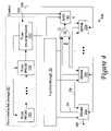
- FIG. 4there is illustrated a second exemplary embodiment of an integrated circuit 12 b in accordance with the present invention.
- integrated circuit 12 bcontains functional logic 20 , multiple memories (e.g., SRAMs) 22 , a BIST circuit 50 , and combination logic (e.g., OR gate 70 ) as described above.
- FIG. 4further depicts an implementation of non-volatile fail storage 80 in which the defect repair remappings for SRAMs 22 are compressed together with the defect repair remappings of one or more other memories for more compact storage within fuse PROMs 140 .
- fuse decompression logic 142When control (e.g., POR) signal 150 is asserted, fuse decompression logic 142 sequences accesses to fuse PROMs 140 to read out and decompress the defect repair remappings, which are transmitted in a serial stream to SRAMs 22 via serial bus 146 .
- controle.g., POR
- fuse decompression logic 142sequences accesses to fuse PROMs 140 to read out and decompress the defect repair remappings, which are transmitted in a serial stream to SRAMs 22 via serial bus 146 .
- common remappings applicable to all of SRAMs 22are stored by RRF 40 within each of SRAMs 22 .
- the serial stream of defect repair remappingsis also transmitted by SRAM 22 a on serial bus 160 to a next memory or set of memories, which has a different set of defect repair remapping than the common remappings applied to SRAMs 22 .
- the present inventionprovides an improved integrated circuit and method of detecting and repairing defects in embedded memory arrays.
- detected defectsare aggregated across multiple embedded memory arrays to obtain a composite list of failing addresses, and a common address remapping is applied to all of the multiple memory arrays to repair each detected defect.
- the die size devoted to the detection and repair of memory defectsis significantly reduced.
- Such program productswhich may take the form of Verilog, VHDL, or other design language files, can be delivered to a data processing system via a variety of signal-bearing media, which include, without limitation, non-rewritable storage media (e.g., CD-ROM), rewritable storage media (e.g., a floppy diskette or hard disk drive), and communication media, such as digital and analog networks.
- signal-bearing mediawhen carrying or encoding computer readable instructions embodying the present invention, represent alternative embodiments of the present invention.
Landscapes
- For Increasing The Reliability Of Semiconductor Memories (AREA)
- Tests Of Electronic Circuits (AREA)
Abstract
Description
Claims (21)
Priority Applications (1)
| Application Number | Priority Date | Filing Date | Title |
|---|---|---|---|
| US10/604,195US6993692B2 (en) | 2003-06-30 | 2003-06-30 | Method, system and apparatus for aggregating failures across multiple memories and applying a common defect repair solution to all of the multiple memories |
Applications Claiming Priority (1)
| Application Number | Priority Date | Filing Date | Title |
|---|---|---|---|
| US10/604,195US6993692B2 (en) | 2003-06-30 | 2003-06-30 | Method, system and apparatus for aggregating failures across multiple memories and applying a common defect repair solution to all of the multiple memories |
Publications (2)
| Publication Number | Publication Date |
|---|---|
| US20040268198A1 US20040268198A1 (en) | 2004-12-30 |
| US6993692B2true US6993692B2 (en) | 2006-01-31 |
Family
ID=33539942
Family Applications (1)
| Application Number | Title | Priority Date | Filing Date |
|---|---|---|---|
| US10/604,195Expired - LifetimeUS6993692B2 (en) | 2003-06-30 | 2003-06-30 | Method, system and apparatus for aggregating failures across multiple memories and applying a common defect repair solution to all of the multiple memories |
Country Status (1)
| Country | Link |
|---|---|
| US (1) | US6993692B2 (en) |
Cited By (12)
| Publication number | Priority date | Publication date | Assignee | Title |
|---|---|---|---|---|
| US20040196022A1 (en)* | 2002-12-18 | 2004-10-07 | Infineon Technologies Ag | Semiconductor device testing apparatus, system, and method for testing the contacting with semiconductor devices positioned one upon the other |
| US20060031789A1 (en)* | 2004-07-22 | 2006-02-09 | Elias Gedamu | Built-in self-test emulator |
| US20070022360A1 (en)* | 2005-06-30 | 2007-01-25 | Nivruti Rai | Method and apparatus to lower operating voltages for memory arrays using error correcting codes |
| EP1791133A1 (en)* | 2005-11-29 | 2007-05-30 | STMicroelectronics Pvt. Ltd. | A method of sharing testing components for multiple embedded memories and the memory system incorporating the same |
| US20080209283A1 (en)* | 2007-02-23 | 2008-08-28 | Freescale Semiconductor, Inc. | Shared latch for memory test/repair and functional operations |
| US20090249146A1 (en)* | 2008-03-26 | 2009-10-01 | International Business Machines Corporation | Automatically extensible addressing for shared array built-in self-test (abist) circuitry |
| US20090300413A1 (en)* | 2006-06-21 | 2009-12-03 | Chang Tsung-Yung Jonathan | Disabling portions of memory with defects |
| US20100131812A1 (en)* | 2008-11-26 | 2010-05-27 | Qualcomm Incorporated | Resizable Cache Memory |
| US20130227344A1 (en)* | 2012-02-29 | 2013-08-29 | Kyo-Min Sohn | Device and method for repairing memory cell and memory system including the device |
| US8570820B2 (en) | 2011-03-08 | 2013-10-29 | International Business Machines Corporation | Selectable repair pass masking |
| US20170110206A1 (en)* | 2012-02-29 | 2017-04-20 | Samsung Electronics Co., Ltd. | Semiconductor memory devices and methods of operating the same |
| US9653183B1 (en) | 2016-09-01 | 2017-05-16 | Qualcomm Incorporated | Shared built-in self-analysis of memory systems employing a memory array tile architecture |
Families Citing this family (4)
| Publication number | Priority date | Publication date | Assignee | Title |
|---|---|---|---|---|
| US7999388B2 (en)* | 2007-09-24 | 2011-08-16 | Research Triangle Institute | Preventing breakage of long metal signal conductors on semiconductor substrates |
| US7752518B2 (en)* | 2008-02-13 | 2010-07-06 | Texas Instruments Incorporated | System and method for increasing the extent of built-in self-testing of memory and circuitry |
| US8004915B1 (en)* | 2009-05-08 | 2011-08-23 | Altera Corporation | Area-efficient memory built-in-self-test circuitry with advanced debug capabilities for distributed memory blocks |
| US9384856B2 (en)* | 2013-12-11 | 2016-07-05 | Freescale Semiconductor, Inc. | Memories having a built-in self-test (BIST) feature |
Citations (17)
| Publication number | Priority date | Publication date | Assignee | Title |
|---|---|---|---|---|
| US4333142A (en) | 1977-07-22 | 1982-06-01 | Chesley Gilman D | Self-configurable computer and memory system |
| US5222066A (en) | 1990-12-26 | 1993-06-22 | Motorola, Inc. | Modular self-test for embedded SRAMS |
| US5388104A (en) | 1990-12-27 | 1995-02-07 | Kabushiki Kaisha Toshiba | Semiconductor integrated circuit capable of testing memory blocks |
| US5475815A (en) | 1994-04-11 | 1995-12-12 | Unisys Corporation | Built-in-self-test scheme for testing multiple memory elements |
| US5535164A (en) | 1995-03-03 | 1996-07-09 | International Business Machines Corporation | BIST tester for multiple memories |
| US5617531A (en) | 1993-11-02 | 1997-04-01 | Motorola, Inc. | Data Processor having a built-in internal self test controller for testing a plurality of memories internal to the data processor |
| US5835502A (en) | 1996-06-28 | 1998-11-10 | International Business Machines Corporation | Method and apparatus for handling variable data word widths and array depths in a serial shared abist scheme |
| US5974579A (en) | 1996-09-03 | 1999-10-26 | Credence Systems Corporation | Efficient built-in self test for embedded memories with differing address spaces |
| US5995731A (en) | 1997-12-29 | 1999-11-30 | Motorola, Inc. | Multiple BIST controllers for testing multiple embedded memory arrays |
| US6085346A (en) | 1996-09-03 | 2000-07-04 | Credence Systems Corporation | Method and apparatus for built-in self test of integrated circuits |
| US6163490A (en)* | 1998-02-25 | 2000-12-19 | Micron Technology, Inc. | Semiconductor memory remapping |
| US6209074B1 (en)* | 1998-04-28 | 2001-03-27 | International Business Machines Corporation | Address re-mapping for memory module using presence detect data |
| US6360342B1 (en) | 1998-06-23 | 2002-03-19 | National Science Council | Built-in self test for multiple memories in a chip |
| US20020046377A1 (en) | 1999-03-17 | 2002-04-18 | Oliver Kniffler | Method for built-in self test of an electronic circuit |
| US6446184B2 (en)* | 1998-04-28 | 2002-09-03 | International Business Machines Corporation | Address re-mapping for memory module using presence detect data |
| US20020174394A1 (en) | 2001-05-16 | 2002-11-21 | Ledford James S. | External control of algorithm execution in a built-in self-test circuit and method therefor |
| US20030016578A1 (en) | 2001-07-18 | 2003-01-23 | Thomas Janik | Test of a semiconductor memory having a plurality of memory banks |
- 2003
- 2003-06-30USUS10/604,195patent/US6993692B2/ennot_activeExpired - Lifetime
Patent Citations (17)
| Publication number | Priority date | Publication date | Assignee | Title |
|---|---|---|---|---|
| US4333142A (en) | 1977-07-22 | 1982-06-01 | Chesley Gilman D | Self-configurable computer and memory system |
| US5222066A (en) | 1990-12-26 | 1993-06-22 | Motorola, Inc. | Modular self-test for embedded SRAMS |
| US5388104A (en) | 1990-12-27 | 1995-02-07 | Kabushiki Kaisha Toshiba | Semiconductor integrated circuit capable of testing memory blocks |
| US5617531A (en) | 1993-11-02 | 1997-04-01 | Motorola, Inc. | Data Processor having a built-in internal self test controller for testing a plurality of memories internal to the data processor |
| US5475815A (en) | 1994-04-11 | 1995-12-12 | Unisys Corporation | Built-in-self-test scheme for testing multiple memory elements |
| US5535164A (en) | 1995-03-03 | 1996-07-09 | International Business Machines Corporation | BIST tester for multiple memories |
| US5835502A (en) | 1996-06-28 | 1998-11-10 | International Business Machines Corporation | Method and apparatus for handling variable data word widths and array depths in a serial shared abist scheme |
| US6085346A (en) | 1996-09-03 | 2000-07-04 | Credence Systems Corporation | Method and apparatus for built-in self test of integrated circuits |
| US5974579A (en) | 1996-09-03 | 1999-10-26 | Credence Systems Corporation | Efficient built-in self test for embedded memories with differing address spaces |
| US5995731A (en) | 1997-12-29 | 1999-11-30 | Motorola, Inc. | Multiple BIST controllers for testing multiple embedded memory arrays |
| US6163490A (en)* | 1998-02-25 | 2000-12-19 | Micron Technology, Inc. | Semiconductor memory remapping |
| US6209074B1 (en)* | 1998-04-28 | 2001-03-27 | International Business Machines Corporation | Address re-mapping for memory module using presence detect data |
| US6446184B2 (en)* | 1998-04-28 | 2002-09-03 | International Business Machines Corporation | Address re-mapping for memory module using presence detect data |
| US6360342B1 (en) | 1998-06-23 | 2002-03-19 | National Science Council | Built-in self test for multiple memories in a chip |
| US20020046377A1 (en) | 1999-03-17 | 2002-04-18 | Oliver Kniffler | Method for built-in self test of an electronic circuit |
| US20020174394A1 (en) | 2001-05-16 | 2002-11-21 | Ledford James S. | External control of algorithm execution in a built-in self-test circuit and method therefor |
| US20030016578A1 (en) | 2001-07-18 | 2003-01-23 | Thomas Janik | Test of a semiconductor memory having a plurality of memory banks |
Cited By (25)
| Publication number | Priority date | Publication date | Assignee | Title |
|---|---|---|---|---|
| US20040196022A1 (en)* | 2002-12-18 | 2004-10-07 | Infineon Technologies Ag | Semiconductor device testing apparatus, system, and method for testing the contacting with semiconductor devices positioned one upon the other |
| US7251758B2 (en)* | 2002-12-18 | 2007-07-31 | Infineon Technologies Ag | Semiconductor device testing apparatus, system, and method for testing the contacting with semiconductor devices positioned one upon the other |
| US20060031789A1 (en)* | 2004-07-22 | 2006-02-09 | Elias Gedamu | Built-in self-test emulator |
| US20070022360A1 (en)* | 2005-06-30 | 2007-01-25 | Nivruti Rai | Method and apparatus to lower operating voltages for memory arrays using error correcting codes |
| US7581154B2 (en)* | 2005-06-30 | 2009-08-25 | Intel Corporation | Method and apparatus to lower operating voltages for memory arrays using error correcting codes |
| EP1791133A1 (en)* | 2005-11-29 | 2007-05-30 | STMicroelectronics Pvt. Ltd. | A method of sharing testing components for multiple embedded memories and the memory system incorporating the same |
| US8091000B2 (en)* | 2006-06-21 | 2012-01-03 | Intel Corporation | Disabling portions of memory with defects |
| US20090300413A1 (en)* | 2006-06-21 | 2009-12-03 | Chang Tsung-Yung Jonathan | Disabling portions of memory with defects |
| US20100058109A1 (en)* | 2006-06-21 | 2010-03-04 | Chang Tsung-Yung Jonathan | Disabling portions of memory with defects |
| US20080209283A1 (en)* | 2007-02-23 | 2008-08-28 | Freescale Semiconductor, Inc. | Shared latch for memory test/repair and functional operations |
| US7707466B2 (en) | 2007-02-23 | 2010-04-27 | Freescale Semiconductor, Inc. | Shared latch for memory test/repair and functional operations |
| US7757141B2 (en)* | 2008-03-26 | 2010-07-13 | International Business Machines Corporation | Automatically extensible addressing for shared array built-in self-test (ABIST) circuitry |
| US20090249146A1 (en)* | 2008-03-26 | 2009-10-01 | International Business Machines Corporation | Automatically extensible addressing for shared array built-in self-test (abist) circuitry |
| US8127184B2 (en)* | 2008-11-26 | 2012-02-28 | Qualcomm Incorporated | System and method including built-in self test (BIST) circuit to test cache memory |
| US20100131812A1 (en)* | 2008-11-26 | 2010-05-27 | Qualcomm Incorporated | Resizable Cache Memory |
| US8570820B2 (en) | 2011-03-08 | 2013-10-29 | International Business Machines Corporation | Selectable repair pass masking |
| US20150243374A1 (en)* | 2012-02-29 | 2015-08-27 | Kyo-Min Sohn | Device and method for repairing memory cell and memory system including the device |
| US9087613B2 (en)* | 2012-02-29 | 2015-07-21 | Samsung Electronics Co., Ltd. | Device and method for repairing memory cell and memory system including the device |
| US20130227344A1 (en)* | 2012-02-29 | 2013-08-29 | Kyo-Min Sohn | Device and method for repairing memory cell and memory system including the device |
| US20170110206A1 (en)* | 2012-02-29 | 2017-04-20 | Samsung Electronics Co., Ltd. | Semiconductor memory devices and methods of operating the same |
| US9659669B2 (en)* | 2012-02-29 | 2017-05-23 | Samsung Electronics Co., Ltd. | Device and method for repairing memory cell and memory system including the device |
| US9831003B2 (en)* | 2012-02-29 | 2017-11-28 | Samsung Electronics Co., Ltd. | Device and method for repairing memory cell and memory system including the device |
| US9953725B2 (en)* | 2012-02-29 | 2018-04-24 | Samsung Electronics Co., Ltd. | Semiconductor memory devices and methods of operating the same |
| US10347355B2 (en)* | 2012-02-29 | 2019-07-09 | Samsung Electronics Co., Ltd. | Device and method for repairing memory cell and memory system including the device |
| US9653183B1 (en) | 2016-09-01 | 2017-05-16 | Qualcomm Incorporated | Shared built-in self-analysis of memory systems employing a memory array tile architecture |
Also Published As
| Publication number | Publication date |
|---|---|
| US20040268198A1 (en) | 2004-12-30 |
Similar Documents
| Publication | Publication Date | Title |
|---|---|---|
| US6286115B1 (en) | On-chip testing circuit and method for integrated circuits | |
| US6993692B2 (en) | Method, system and apparatus for aggregating failures across multiple memories and applying a common defect repair solution to all of the multiple memories | |
| US5631868A (en) | Method and apparatus for testing redundant word and bit lines in a memory array | |
| EP0555307B1 (en) | A fault tolerant data storage system | |
| US6408401B1 (en) | Embedded RAM with self-test and self-repair with spare rows and columns | |
| JP3274332B2 (en) | Controller / mass memory embedded semiconductor integrated circuit device, test method and use method thereof, and semiconductor integrated circuit device and test method therefor | |
| US7818636B1 (en) | Method and apparatus for improving memory operation and yield | |
| US7149924B1 (en) | Apparatus, method, and system having a pin to activate the self-test and repair instructions | |
| US7415640B1 (en) | Methods and apparatuses that reduce the size of a repair data container for repairable memories | |
| US6091649A (en) | Integrated circuit memory devices having built-in self test based redundancy and methods of operation thereof | |
| US5315552A (en) | Memory module, method for control thereof and method for setting fault bit table for use therewith | |
| US8201037B2 (en) | Semiconductor integrated circuit and method for controlling semiconductor integrated circuit | |
| US20030084386A1 (en) | ECC Based system and method for repairing failed memory elements | |
| JP4481588B2 (en) | Semiconductor integrated circuit device | |
| JP2549272B2 (en) | Integrated circuit | |
| US7454662B2 (en) | Integrated memory having a circuit for testing the operation of the integrated memory, and method for operating the integrated memory | |
| US20080013389A1 (en) | Random access memory including test circuit | |
| US7020033B2 (en) | Semiconductor memory apparatus and self-repair method | |
| US20030204783A1 (en) | Repair analyzer of dram in semiconductor integrated circuit using built-in CPU | |
| US7013414B2 (en) | Test method and test system for semiconductor device | |
| US20050066226A1 (en) | Redundant memory self-test | |
| US7593274B2 (en) | Semiconductor integrated circuit and relief method and test method of the same | |
| CN100492546C (en) | Method for reading defect information items from integrated chip and integrated memory chip | |
| JP2003509804A (en) | Memory inspection method | |
| JP4215723B2 (en) | Integrated circuit |
Legal Events
| Date | Code | Title | Description |
|---|---|---|---|
| AS | Assignment | Owner name:INTERNATIONAL BUSINESS MACHINES CORPORATION, NEW Y Free format text:ASSIGNMENT OF ASSIGNORS INTEREST;ASSIGNORS:OUELLETTE, MICHAEL R;TELLEZ, GUSTAVO ENRIQUE;ZUCHOWSKI, PAUL STEVEN;REEL/FRAME:013765/0679;SIGNING DATES FROM 20030623 TO 20030630 | |
| FEPP | Fee payment procedure | Free format text:PAYOR NUMBER ASSIGNED (ORIGINAL EVENT CODE: ASPN); ENTITY STATUS OF PATENT OWNER: LARGE ENTITY | |
| STCF | Information on status: patent grant | Free format text:PATENTED CASE | |
| FPAY | Fee payment | Year of fee payment:4 | |
| REMI | Maintenance fee reminder mailed | ||
| AS | Assignment | Owner name:TWITTER, INC., CALIFORNIA Free format text:ASSIGNMENT OF ASSIGNORS INTEREST;ASSIGNOR:INTERNATIONAL BUSINESS MACHINES CORPORATION;REEL/FRAME:032075/0404 Effective date:20131230 | |
| FPAY | Fee payment | Year of fee payment:8 | |
| SULP | Surcharge for late payment | Year of fee payment:7 | |
| FPAY | Fee payment | Year of fee payment:12 | |
| AS | Assignment | Owner name:MORGAN STANLEY SENIOR FUNDING, INC., MARYLAND Free format text:SECURITY INTEREST;ASSIGNOR:TWITTER, INC.;REEL/FRAME:062079/0677 Effective date:20221027 Owner name:MORGAN STANLEY SENIOR FUNDING, INC., MARYLAND Free format text:SECURITY INTEREST;ASSIGNOR:TWITTER, INC.;REEL/FRAME:061804/0086 Effective date:20221027 Owner name:MORGAN STANLEY SENIOR FUNDING, INC., MARYLAND Free format text:SECURITY INTEREST;ASSIGNOR:TWITTER, INC.;REEL/FRAME:061804/0001 Effective date:20221027 | |
| AS | Assignment | Owner name:X CORP. (F/K/A TWITTER, INC.), TEXAS Free format text:RELEASE BY SECURED PARTY;ASSIGNOR:MORGAN STANLEY SENIOR FUNDING, INC.;REEL/FRAME:070670/0857 Effective date:20250220 | |
| AS | Assignment | Owner name:X CORP. (F/K/A TWITTER, INC.), TEXAS Free format text:RELEASE BY SECURED PARTY;ASSIGNOR:MORGAN STANLEY SENIOR FUNDING, INC., AS COLLATERAL AGENT;REEL/FRAME:071127/0240 Effective date:20250429 |