US6992932B2 - Method circuit and system for read error detection in a non-volatile memory array - Google Patents
Method circuit and system for read error detection in a non-volatile memory arrayDownload PDFInfo
- Publication number
- US6992932B2 US6992932B2US10/695,457US69545703AUS6992932B2US 6992932 B2US6992932 B2US 6992932B2US 69545703 AUS69545703 AUS 69545703AUS 6992932 B2US6992932 B2US 6992932B2
- Authority
- US
- United States
- Prior art keywords
- cells
- read
- state
- nvm
- programmed
- Prior art date
- Legal status (The legal status is an assumption and is not a legal conclusion. Google has not performed a legal analysis and makes no representation as to the accuracy of the status listed.)
- Expired - Lifetime, expires
Links
- 238000000034methodMethods0.000titleclaimsabstractdescription41
- 238000001514detection methodMethods0.000titledescription17
- 238000012360testing methodMethods0.000description68
- 230000008569processEffects0.000description7
- 230000000875corresponding effectEffects0.000description5
- 238000010586diagramMethods0.000description5
- 238000005070samplingMethods0.000description3
- 230000002596correlated effectEffects0.000description2
- 230000006870functionEffects0.000description2
- 238000012986modificationMethods0.000description2
- 230000004048modificationEffects0.000description2
- 230000000153supplemental effectEffects0.000description2
- 238000011156evaluationMethods0.000description1
- 238000012804iterative processMethods0.000description1
- 230000008520organizationEffects0.000description1
- 238000012545processingMethods0.000description1
- 230000004044responseEffects0.000description1
- 238000006467substitution reactionMethods0.000description1
Images


Classifications
- G—PHYSICS
- G11—INFORMATION STORAGE
- G11C—STATIC STORES
- G11C11/00—Digital stores characterised by the use of particular electric or magnetic storage elements; Storage elements therefor
- G11C11/56—Digital stores characterised by the use of particular electric or magnetic storage elements; Storage elements therefor using storage elements with more than two stable states represented by steps, e.g. of voltage, current, phase, frequency
- G11C11/5621—Digital stores characterised by the use of particular electric or magnetic storage elements; Storage elements therefor using storage elements with more than two stable states represented by steps, e.g. of voltage, current, phase, frequency using charge storage in a floating gate
- G11C11/5642—Sensing or reading circuits; Data output circuits
- G—PHYSICS
- G11—INFORMATION STORAGE
- G11C—STATIC STORES
- G11C16/00—Erasable programmable read-only memories
- G11C16/02—Erasable programmable read-only memories electrically programmable
- G11C16/06—Auxiliary circuits, e.g. for writing into memory
- G11C16/26—Sensing or reading circuits; Data output circuits
- G11C16/28—Sensing or reading circuits; Data output circuits using differential sensing or reference cells, e.g. dummy cells
- G—PHYSICS
- G11—INFORMATION STORAGE
- G11C—STATIC STORES
- G11C16/00—Erasable programmable read-only memories
- G11C16/02—Erasable programmable read-only memories electrically programmable
- G11C16/06—Auxiliary circuits, e.g. for writing into memory
- G11C16/34—Determination of programming status, e.g. threshold voltage, overprogramming or underprogramming, retention
- G11C16/3436—Arrangements for verifying correct programming or erasure
- G11C16/3454—Arrangements for verifying correct programming or for detecting overprogrammed cells
- G11C16/3459—Circuits or methods to verify correct programming of nonvolatile memory cells
- G—PHYSICS
- G11—INFORMATION STORAGE
- G11C—STATIC STORES
- G11C29/00—Checking stores for correct operation ; Subsequent repair; Testing stores during standby or offline operation
- G11C29/02—Detection or location of defective auxiliary circuits, e.g. defective refresh counters
- G11C29/026—Detection or location of defective auxiliary circuits, e.g. defective refresh counters in sense amplifiers
- G—PHYSICS
- G11—INFORMATION STORAGE
- G11C—STATIC STORES
- G11C29/00—Checking stores for correct operation ; Subsequent repair; Testing stores during standby or offline operation
- G11C29/02—Detection or location of defective auxiliary circuits, e.g. defective refresh counters
- G11C29/028—Detection or location of defective auxiliary circuits, e.g. defective refresh counters with adaption or trimming of parameters
- G—PHYSICS
- G11—INFORMATION STORAGE
- G11C—STATIC STORES
- G11C29/00—Checking stores for correct operation ; Subsequent repair; Testing stores during standby or offline operation
- G11C29/04—Detection or location of defective memory elements, e.g. cell constructio details, timing of test signals
- G11C29/08—Functional testing, e.g. testing during refresh, power-on self testing [POST] or distributed testing
- G11C29/12—Built-in arrangements for testing, e.g. built-in self testing [BIST] or interconnection details
- G11C29/18—Address generation devices; Devices for accessing memories, e.g. details of addressing circuits
- G11C29/24—Accessing extra cells, e.g. dummy cells or redundant cells
- G—PHYSICS
- G11—INFORMATION STORAGE
- G11C—STATIC STORES
- G11C29/00—Checking stores for correct operation ; Subsequent repair; Testing stores during standby or offline operation
- G11C29/04—Detection or location of defective memory elements, e.g. cell constructio details, timing of test signals
- G11C29/08—Functional testing, e.g. testing during refresh, power-on self testing [POST] or distributed testing
- G11C29/12—Built-in arrangements for testing, e.g. built-in self testing [BIST] or interconnection details
- G11C29/38—Response verification devices
- G11C29/42—Response verification devices using error correcting codes [ECC] or parity check
- G—PHYSICS
- G11—INFORMATION STORAGE
- G11C—STATIC STORES
- G11C29/00—Checking stores for correct operation ; Subsequent repair; Testing stores during standby or offline operation
- G11C29/52—Protection of memory contents; Detection of errors in memory contents
- G—PHYSICS
- G11—INFORMATION STORAGE
- G11C—STATIC STORES
- G11C16/00—Erasable programmable read-only memories
- G11C16/02—Erasable programmable read-only memories electrically programmable
- G11C16/04—Erasable programmable read-only memories electrically programmable using variable threshold transistors, e.g. FAMOS
- G—PHYSICS
- G11—INFORMATION STORAGE
- G11C—STATIC STORES
- G11C16/00—Erasable programmable read-only memories
- G11C16/02—Erasable programmable read-only memories electrically programmable
- G11C16/06—Auxiliary circuits, e.g. for writing into memory
- G11C16/34—Determination of programming status, e.g. threshold voltage, overprogramming or underprogramming, retention
- G11C16/3436—Arrangements for verifying correct programming or erasure
- G—PHYSICS
- G11—INFORMATION STORAGE
- G11C—STATIC STORES
- G11C29/00—Checking stores for correct operation ; Subsequent repair; Testing stores during standby or offline operation
- G11C29/04—Detection or location of defective memory elements, e.g. cell constructio details, timing of test signals
- G11C2029/0409—Online test
- G—PHYSICS
- G11—INFORMATION STORAGE
- G11C—STATIC STORES
- G11C29/00—Checking stores for correct operation ; Subsequent repair; Testing stores during standby or offline operation
- G11C29/04—Detection or location of defective memory elements, e.g. cell constructio details, timing of test signals
- G11C29/08—Functional testing, e.g. testing during refresh, power-on self testing [POST] or distributed testing
- G11C29/12—Built-in arrangements for testing, e.g. built-in self testing [BIST] or interconnection details
- G11C2029/4402—Internal storage of test result, quality data, chip identification, repair information
- G—PHYSICS
- G11—INFORMATION STORAGE
- G11C—STATIC STORES
- G11C2211/00—Indexing scheme relating to digital stores characterized by the use of particular electric or magnetic storage elements; Storage elements therefor
- G11C2211/56—Indexing scheme relating to G11C11/56 and sub-groups for features not covered by these groups
- G11C2211/563—Multilevel memory reading aspects
- G11C2211/5634—Reference cells
- G—PHYSICS
- G11—INFORMATION STORAGE
- G11C—STATIC STORES
- G11C2211/00—Indexing scheme relating to digital stores characterized by the use of particular electric or magnetic storage elements; Storage elements therefor
- G11C2211/56—Indexing scheme relating to G11C11/56 and sub-groups for features not covered by these groups
- G11C2211/564—Miscellaneous aspects
- G11C2211/5644—Multilevel memory comprising counting devices
- G—PHYSICS
- G11—INFORMATION STORAGE
- G11C—STATIC STORES
- G11C29/00—Checking stores for correct operation ; Subsequent repair; Testing stores during standby or offline operation
Definitions
- the present inventiongenerally relates to the field of non-volatile memory (“NVM”) cells. More specifically, the present invention relates to a method and a system for selecting a reference voltage of one or more reference cells in order to read one or more memory cells within a memory cell array.
- NVMnon-volatile memory
- NVM cellsare generally operated (e.g. programmed, read, and erased) using one or more reference structures or cells. Each of the one or more reference structures or cells may be compared against a memory cell being operated in order to determine a condition or state of the memory cell being operated.
- an NVM cell's statemay be defined and determined by its threshold voltage, the voltage at which the cell begins to conduct current.
- a NVM cell's threshold voltage levelis usually correlated to the amount of charge stored in a charge storage region of the cell. Different threshold voltage ranges are associated with different states of an NVM cell.
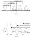
- FIG. 1Ashows a graph depicting the boundaries between the two states, erased and programmed, of a binary NVM cell, and the buffer region in between the two states.
- the cell's threshold levelis compared to that of a reference structure or cell whose threshold level is set, or otherwise known to be, at a voltage level associated with the specific state being tested for. Comparing the threshold voltage of a NVM cell to that of a reference cell is often accomplished using a sense amplifier or similar circuit.
- Various techniques for comparing an NVM's threshold voltage against those of one or more reference cells or structures, in order to determine the NVM's cells stateare well known and applicable to the present invention. Any method or circuit presently known or to be devised in the future for comparing threshold voltage levels of reference cells or structures against NVM cells are applicable to the present invention.
- an NVM cell's threshold valuemay be compared against a reference cell having a reference threshold value set at a voltage level defined as the “program verify” level.
- the reference cell with a threshold voltage set at a voltage level defined as a “program verify” level for the given statemay be compared to the threshold voltage of the cell being programmed (i.e. charged) in order to determine whether a charge storage area or region of the cell being programmed has been sufficiently charged so as to have placed the cell in a condition which may be considered “programmed” at the desired state.
- the cell's threshold voltagemay be compared against that of a reference cell having a reference threshold voltage defined as a “read” level for the specific state.
- a “read” levelis usually set lower than a “program verify” level and higher than the erase verify level in order to compensate for voltage drifts which may occur during operation.
- a logical state of the cellis defined as ‘0’ if the cell's Vt is higher than that of the read reference and ‘1’ if it is lower.
- two or more programming levelsmay co-exist on the same cell, as is drawn in FIG. 1B .
- at least two read reference cellsmust be used.
- the MLC cell's thresholdis in one of three or more regions bounded by the two or more threshold voltages defined by read reference cells.
- the voltage threshold boundaries which define a given state in an MLCare usually considerably smaller than those for a binary NVM cell.
- FIG. 1Billustrates four different threshold voltage regions of an MLC, where each region is associated with either one of the programmed states of the MLC or with the erased state of the MLC.
- a rather fixed range of potential threshold voltagese.g. 3 Volts to 9 Volts
- the size of each sub-range or region in an MLCis usually smaller than a region of a binary NVM cell, which binary cell only requires two voltage threshold regions, as seen in FIG. 1A .
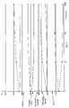
- FIG. 2shows a graph depicting threshold voltages (V t ) changes associated with two program states of an exemplary MLC due to drift, as a function of time, for 10 cycles and for 1000 cycles. As seen in the graph, voltage drift may occur across numerous cells, and may occur in a correlated pattern across these cells.
- V tdeviations in cells'
- Variation of the threshold voltage of memory cellsmay lead to false reads of the state and may further result in the corruption of the data in the memory array. Voltage drift is especially problematic in MLC cells where the V t regions or sub-ranges associated with each programmed state are relatively smaller than those for a typical binary cell.
- threshold voltage drift of cells in the NVM arrayshould be compensated for.
- There is a well understood need for an efficient and reliable method of determining a set of reference voltage levelswhich may accommodate variations in the threshold voltages of cells of an NVM array, and of established reference cells with the determined reference voltages.
- the present inventionis a method, circuit and system for determining a reference voltage.
- Some embodiments of the present inventionrelate to a system, method and circuit for establishing a set of operating reference cells to be used in operating (e.g. reading) cells in a NVM block or array.
- at least a subset of cells of the NVM block or arraymay be read using each of two or more sets of test reference cells, where each set of test reference cells may generate or otherwise provide reference voltages at least slightly offset from each other set of test reference cells.
- a read error ratemay be calculated or otherwise determined.
- a set of test reference cells associated with a relatively low read error ratemay be selected as the set of operating reference cells to be used in operating (e.g. reading) other cells, outside the subset of cells, in the NVM block or array.
- the selected set of test reference cellsmay be used to establish an operating set of reference cells having reference voltages substantially equal to those of the selected test set.
- the number of cells to be programmed to each of one or more logical or program states associated with the set of cellsmay be counted, and may be stored, for example in a check sum table.
- the number of cells to be programmed to, up to and/or below each logical or program statemay be counted and/or stored in a table with is either on the same array as the set of NVM cells or in memory on the same chip as the NVM array.
- the number of cells found to be at a given logical or program statemay be compared against either corresponding values stored during programming (e.g. the number of cells programmed to a given state) or against a value derived from the values stored during programming (e.g. the number of cells programmed at or above the given state, minus the number of cells programmed to or above an adjacent higher logical state). If there is a discrepancy between the number of cells read at a given state and an expected number based on the values determined/counted/stored during programming, a Read Verify reference threshold value associated with the given program state may be adjusted upward or downward to compensate for the detected error. According to some embodiments of the present invention, the read verify level of an adjacent logical state may also be moved upward or downward in order to compensate for detected read errors at a given state.
- the Read Verify reference voltage associated with that given statemay be reduced, or if there is found that the number of cells read above the given state exceeds an expected number, the Read Verify reference associated with a logical state higher and adjacent to the given state may be raised.
- the Read Verify reference voltage associated with that given statemay be increased, or if there is found that the number of cells read above the given state is below an expected number, the Read Verify reference associated with a logical state higher and adjacent to the given state may be lowered.
- Read Verify reference voltages for a set of cellsmay be selected such that the number of cells found/read in each of the states associated with the set may be substantially equal to the a number either read from or derived from the values counted during programming of the set of cells, which values may have been stored in a check sum table.
- the check sum tablemay reside on the same chip as the set of NVM cells, and according to a further embodiment of the present invention, a controller may be adapted to perform the above mentioned error detection and Read Verify reference value adjustments.
- the check sum tablemay either be stored in the same NVM array as the set of NVM cells, or on some other memory cells residing on the same chip as the NVM array, for example in a register or buffer used by the controller during programming and/or reading.
- specialized error coding and detection circuitsmay be included with a controller on the same chip and the NVM array to be operated.
- FIG. 1Ais a graphical illustration of the different threshold voltages associated with the different states of a binary NVM cell, where both the Program Verify and Read Verify Threshold Levels are visible, and;
- FIG. 1Bis a graphical illustration of different threshold voltages, each being associated with the boundary of a different program state of a Multi-Level Cell (MLC);
- MLCMulti-Level Cell
- FIG. 2is a graph illustrating measured changes in the threshold voltages (V t ) associated with each program state of an exemplary Multi Level Cell (MLC) due to V t drift, as a function of time, for 10 cycles and for 1000 cycles;
- V tthreshold voltages
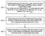
- FIG. 3is a flow chart illustration of a method of selecting a set of reference cells to be used in operating an NVM block or array, in accordance with some embodiments of the present invention
- FIG. 4is a block diagram illustration of one possible circuit configuration associated with a NVM array supporting one implementation of the method of FIG. 3 , according to some embodiments of the present invention.
- FIG. 5is a block diagram illustration of one possible circuit configuration associated with a NVM array for establishing and using a set of operating reference cells having reference voltages substantially equal to those of a selected test set.
- FIG. 6is a block diagram illustration of one possible circuit configuration associated with a NVM array for performing a checks sum based error detection algorithm and for selecting a set of reference cells based on the results of the check sum algorithm, according to some embodiments of the present invention
- FIG. 7Ashows a flow chart listing basic steps of a check sum algorithm according to some embodiments of the present invention.
- FIG. 7Bshows a flow chart listing steps by which the check sum algorithm may be used to adjust a reference voltage (e.g. Read Verify) associated with the reading of cells at a given program state, according to some embodiments of the present invention
- FIGS. 8A & 8Bshow two examples of sets of check sum values which may be stored and used as part of a check sum algorithm according to some embodiments of the present invention.
- the present inventionis a method, circuit and system for determining a reference voltage.
- Some embodiments of the present inventionrelate to a system, method and circuit for establishing a set of operating reference cells to be used in operating (e.g. reading) cells in a NVM block or array.
- at least a subset of cells of the NVM block or arraymay be read using each of two or more sets of test reference cells, where each set of test reference cells may generate or otherwise provide reference voltages at least slightly offset from each other set of test reference cells.
- a read error ratemay be calculated or otherwise determined.
- a set of test reference cells associated with a relatively low read error ratemay be selected as the set of operating reference cells to be used in operating (e.g. reading) other cells, outside the subset of cells, in the NVM block or array.
- the selected set of test reference cellsmay be used to establish (e.g. program) an operating set of reference cells having reference voltages substantially equal to those of the selected test set.
- FIG. 3is a flow chart illustration of the steps of a method of selecting a set of reference cells to be used in operating an NVM block or array, in accordance with some embodiments of the present invention.
- a set counter ‘n’may initially be set to 1 (block 310 ).
- the n th set of test reference cells, initially the 1 st setmay be used to read at least a subset of the NVM block (block 320 ).
- the data read at block 320may be used to determine a read error rate associated with the n th set of test reference cells (block 330 ).
- the at least a subset of the NVM blockmay be a predefined portion or segment of the NVM block where source data is stored on the NVM cells along with extra error detection data/codes derived during programming.
- the read error ratemay be determined using a variety of error rate sampling and/or error detection techniques, for example, parity bit, checksum, CRC and various other techniques. Any error detection coding and/or evaluation technique, presently known or to be devised in the future, may be applicable to present invention.
- the error rate associated with the n th set of test reference cellsmay be recorded (block 340 ).
- the counter ‘n’may then be incremented by 1 (block 350 ), and the counter may be checked to see whether the new ‘n’ is equal to N+1, a value greater than the total number of test reference cell sets (block 360 ). In case that the new ‘n’ is smaller (not equal) than N+1 blocks 320 – 360 may be repeated, and thus an error rate associated with the use of each of the test reference cell sets to read the at least a subset of the NVM block may be determined and recorded.
- the set of reference test cells associated with a relatively low (e.g. the lowest) read error ratemay be selected (block 370 ).
- the selected set of reference cellsmay either be used to operate the cell on NVM block or array (block 380 ), or may be used to establish an operating set of reference cells whose reference threshold voltages substantially correspond to the reference threshold voltages of the selected set (block 390 ), such that the established operating set may be used to operate cells in the NVM array.
- the above descriptionexemplifies one embodiment of a method of establishing a set of operating reference cells to be used in operating a NVM block of cells or array. It should be noted that other embodiments of the present invention may deviate from the above description.
- the selected testmay used as an operating reference set, may be used to select or program an operating set, or may be used to adjust reference levels on a set of adjustable reference structures.
- the method of the present inventionmay be implemented in a variety of implementations including hardware and/or software modules which may be known in the present or yet to be devised in the future.
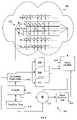
- One example of a possible implementation of a method of establishing a set of operating reference cells to be used in operating cells of a NVM block or array in accordance with the some embodiments of the present inventionis described herein below with reference to FIG. 4 .
- circuitry 401 for operating the NVM block or array 400may include a controller 410 , a controllable voltage supply 412 , a sense amplifier 414 and two or more sets of test reference cells 432 , 434 and 436 .
- Each set of test reference cells 432 , 434 and 436may include two or more test reference cells.
- Each set of test reference cells 432 , 434 and 436may have reference voltages at least slightly offset from each other set of test reference cells. For example, each set of test reference cells (e.g.
- each setmay be associated with a series of threshold voltages that are slightly higher than a corresponding series of threshold voltages associated with the previous set of test reference cells (excluding the first set).
- the controller 410may implement the counter ‘n’ (not shown). However, any other configuration may also be used, including, but not limited to, a distinctive counter module.
- the controller 410may be configured to control the operation of the controllable voltage source 412 and of the sense amplifier 414 . In accordance with some embodiments of the present invention, such as the one illustrated in FIG. 3 , the controller 410 may initially set the reference test set counter ‘n’ to 1. Next, the controller 410 may operate the controllable voltage source 412 , and use the n th set of test reference cells (initially the first set 432 ) to read at least a subset of cells 402 of the NVM block or array.
- the controller 410may instruct the voltage source 412 to apply incrementally increasing voltage pulses to each of the memory cells in the subset area 402 and to one or more test reference cells from the n th set of test reference cells (e.g. 432 ).
- the threshold voltage of each of the memory cells in the subset area 402may be compared, for example using sense amplifier 414 , against the threshold voltages of one or more of the test reference cells in the nth set of test reference cells (e.g. 432 ).
- the state of each of the cells in the subset of cells 402may be read or determined.
- Various other techniques for comparing a memory cell's threshold voltage against those of one or more reference cells and/or structures, in order to determine the memory cell's stateare well known, and may be implemented in accordance with further embodiments of the present invention.
- the controller 410may receive the data read from the NVM cells in the subset area 402 .
- the controller 410may process the data, and may determine a read error rate associated with the n th set of test reference cells used to read the memory cells in the subset area 402 .
- the read error ratemay be determined using a variety of error rate sampling and/or error detection techniques, for example, parity bit, checksum, CRC and various other techniques.
- the subset area 402 and/or any of the other elements of the NVM block 400 and/or the supplementary circuitry 401may be configured to support the error rate sampling and/or error detection technique of choice.
- the subset area 402may include one or more parity bits (marked P n ) in support of parity check error detection.
- the controller 410may be configured to process the data read from the subset area 402 and to determine a read error rate in accordance with parity check error detection.
- a separate error coding and detection circuit(not shown) may be included.
- the controller 410may record the read error rate for each set of test reference cells or structures either internally or in a designated error rate table 416 , which error rate table may be a part of the NVM block or array.
- the read error ratemay be recorded in a manner to maintain the association of each of the recorded read error rates with the set of test reference cells that was used to generate it.
- the countermay be instructed to increment ‘n’ by 1.
- the controller 410may be consulted to check whether the new value for ‘n’ has exceeded the total number of test reference cell sets. If so, the process of determining and recording a read error rate associated with each of the sets of test reference cells may be discontinued by the controller 410 . In other words, the process of determining and recording a read error rate may be repeated for each of the N sets of test reference cells (e.g. 432 , 434 and 436 ).
- the controller 410may then select from amongst the recorded read error rates a relatively low (e.g. the lowest) read error rate.
- the set of test reference cells associated with the selected relatively low read error ratemay be selected as the set of operation reference cells to be used in operating cells of the NVM block or array 400 .
- the controller 410may also determine a set of reference voltages associated with the selected test set associated with the selected relatively low read error rate.
- the set of reference voltagesmay also be recorded, for example in the error rate table 416 .
- the set of reference voltagesmay be stored, such that the association of the stored set of reference voltages with the selected set of test reference cells (e.g. 432 ) is maintained.
- the controller 410determines that more than one of the generated read error rates, each being associated with a different set of test reference cells, is the lowest, for example, when two or more equal read error rates are equally the lowest, additional processing may be required to determine which of the sets is more likely to provide a lower read error rate. For example, the process of generating and recording a read error rate for each of the two or more sets of test reference cells may be repeated in accordance with different criteria or on an additional subset of the NVM block. Alternatively, one of the lowest read error rates may be arbitrarily selected.
- the read error ratemay be checked.
- the set of test reference cells associated with that read error ratemay be selected and recorded, and the process of generating and recording a read error rate may be discontinued prior to checking all the test sets.
- the lowest error ratemay be selected in accordance with the above discussion.
- the selected set of test reference cellsmay be used to establish an operating set of reference cells having reference voltages substantially equal to those of the selected test set.
- FIG. 5is an illustration of one possible configuration of a NVM array for establishing and using a set of operating reference cells having reference voltages substantially equal to those of a selected test set.
- the supplemental circuitry 401 shown in FIG. 5may be substantially similar to that shown in FIG. 4 and may operate in a similar manner, with the addition of a set of global reference cells 520 and an offset circuit 510 .
- the supplemental circuitry 401 and the NVM block 400may be operated to determine a read error rate associated with each one of the two or more sets of test reference cells 432 , 434 and 436 , and to select one of the two or more sets of test reference cells 432 , 434 and 436 associated with a relatively low (e.g. the lowest) read error rate.
- the selected set of test reference cellsmay be used to determine offset values for one or more global reference cells from the set of global reference cells 520 .
- the offset valuesmay be input to an offset circuit 510 , either directly or via the controller 410 .
- the offset circuit 510may be adapted to offset one or more reference voltages of global reference cells from the set of global reference cells 510 .
- the offset circuit 510may be configured to offset the reference voltages of the global reference cells, such that the reference voltages of reference cells in the global reference set 520 may be substantially equal to corresponding reference cells in the selected test set.
- a set of reference voltages associated with the selected test setmay be obtained by the controller 410 .
- the set of reference voltagesmay be recorded, for example in the error rate table 416 .
- the set of reference voltages datamay be obtained by simply retrieving the relevant data from the table 416 .
- the controller 410may instruct the offset circuit 5120 to offset the threshold voltages of one or more of the reference cells in the set of global reference cells 520 in accordance with the set of reference voltages.
- the controller 410may instruct the offset circuit 510 to offset the reference voltages of one or more of the global reference cells in the set of global reference cells 510 , such that the threshold voltages of the set of global reference cells 510 may be substantially equal to the threshold voltages of the selected test set.
- the offset circuit 510 and the set of global reference cells 520may be substituted with a bank of reference cells (not shown).
- the bank of reference cellsmay include two or more reference cells each reference cell in the bank being incrementally offset from the other reference cells in the bank.
- each reference cell in the bankmay have a threshold voltage that is slightly higher than the threshold voltage of the previous reference cell (excluding the first reference cell).
- the selected set of test reference cellsmay be used to determine which of the reference cells in the bank of reference cells is to be used for establishing an operating set of reference cells.
- the selected set of reference cells from the bank of reference cellsmay be selected such that the selected set from the bank may have reference voltages that are substantially equal to those of the selected test set.
- the selected set of reference cells from the bankmay provide a set of operating reference cells having reference voltages substantially equal to those of the selected test set.
- the set of operating reference cellsmay be used to operate the NVM array.
- the number of cells to be programmed to each of one or more logical or program states associated with the set of cellsmay be counted, and may be stored, for example in a check sum table.
- the number of cells to be programmed to, up to and/or below each logical or program statemay be counted and/or stored in a table with is either on the same array as the set of NVM cells or in memory on the same chip as the NVM array.
- the number of cells found to be at a given logical or program statemay be compared against either corresponding values stored during programming (e.g. the number of cells programmed to a given state) or against a value derived from the values stored during programming (e.g. the number of cells programmed at or above the given state, minus the number of cells programmed to or above an adjacent higher logical state). If there is a discrepancy between the number of cells read at a given state and an expected number based on the values determined/counted/stored during programming, a Read Verify reference threshold value associated with the given program state may be adjusted upward or downward to compensate for the detected error. According to some embodiments of the present invention, the read verify level of an adjacent logical state may also be moved upward or downward in order to compensate for detected read errors at a given state.
- the Read Verify reference voltage associated with that given statemay be reduced, or if there is found that the number of cells read above the given state exceeds an expected number, the Read Verify reference associated with a logical state higher and adjacent to the given state may be raised.
- the Read Verify reference voltage associated with that given statemay be increased, or if there is found that the number of cells read above the given state is below an expected number, the Read Verify reference associated with a logical state higher and adjacent to the given state may be lowered.
- Read Verify reference voltages for a set of cellsmay be selected such that the number of cells found/read in each of the states associated with the set may be substantially equal to the a number either read from or derived from the values counted during programming of the set of cells, which values may have been stored in a check sum table.
- the check sum tablemay reside on the same chip as the set of NVM cells, and according to a further embodiment of the present invention, a controller may be adapted to perform the above mentioned error detection and Read Verify reference value adjustments.
- the check sum tablemay either be stored in the same NVM array as the set of NVM cells, or on some other memory cells residing on the same chip as the NVM array, for example in a register or buffer used by the controller during programming and/or reading.
- specialized error coding and detection circuitsmay be included with a controller on the same chip and the NVM array to be operated.
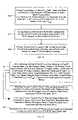
- FIG. 6there is shown a block diagram illustration of one possible circuit configuration associated with a NVM array for performing a check sum based error detection algorithm and for selecting a set of reference cells based on the results of the check sum algorithm.
- FIG. 6in conjunction with FIG. 7A , which shows a flow chart listing the basic steps of a check sum algorithm according to some embodiments of the present invention, there is shown that either prior or during the programming of some number of NVM cells, for example 1000 cells, the number of cells to be programmed either at, above or below each program state associated with the set of cells may be counted (Block 600 ). The counting may possibly be performed by a controller 410 , and the results may be stored in a check sum table 418 .
- the check sum 418 tablemay be stored on the same chip as the NVM array, either directly on the NVM array or on another memory, for example on a storage register or buffer also used by the controller 410 during programming and or reading of the NVM array.
- FIGS. 8A & 8Bthere are shown two examples of how check sum values which may be counted, stored and used as part of a check sum algorithm according to some embodiments of the present invention.
- FIG. 8Aillustrates the counting of cells such that the check sum values for a set of cells are based on the number of cells below each logical or program state
- FIG. 8Billustrated the counting of cells such that the check sum values for a set of cells are based on the number of cells above each logical program state.
- program statemay be defined as any logical state other than an erase state.
- FIGS. 8A & 8Bone of ordinary skill in the art should, should, know that there are a variety of methods and arrangement by which to produce check sum values to be used to determine the number cells programmed to each of the program states associated with a set of NVM cells.
- either the controller 410 or some other error detection circuitmay compare the number of cells counted in each program state during reading with the correspond check sum values stored during or prior to programming. For example, if the total number of cells in the set is 1000, the number of cells read in the third program state is 235, and one of the check sum values stored indicates that the number of cells programmed below the third program state is 750, it can be derived that there should be 250 cells programmed to the third program state and thus the reading of the set missed 15 cells which should have been read as being programmed to the third program state (Block 610 ).
- the Read Verify reference threshold voltage associated with each program statemay be adjusted in response to an error detected in reading during step 610 (block 620 ).
- FIG. 7Bshows a flow chart listing steps by which the check sum algorithm may be used to adjust a reference voltage (e.g. Read Verify) associated with the reading of cells at one or more program states, according to some embodiments of the present invention.
- a reference voltagee.g. Read Verify
- FIG. 7Bshows that if the number of cell's found in a given program state exceed the value derived from the check sum values, the read verify threshold value associated with that given program state may be raised or the Read Verify reference level associated with the adjacent higher state may be lowered. Conversely, if the number of cell's found in a given program state is below the expected number, either the read verify threshold value associated with the given program state may be lowered, or the read verify threshold value associated with the next higher adjacent state may be raised.
- a reference voltagee.g. Read Verify
- the Read Verify reference voltage associated with that given statemay be reduced, or if there is found that the number of cells read above the given state exceeds an expected number, the Read Verify reference associated with a logical state higher and adjacent to the given state may be raised. Conversely, if the number of cells found (e.g. read) in a given program state is below an expected value, either the Read Verify reference voltage associated with that given state may be reduced, or if there is found that the number of cells read above the given state exceeds an expected number, the Read Verify reference associated with a logical state higher and adjacent to the given state may be raised. Conversely, if the number of cells found (e.g. read) in a given program state is below an expected value, either the Read Verify reference voltage associated with that given state may be reduced, or if there is found that the number of cells read above the given state exceeds an expected number, the Read Verify reference associated with a logical state higher and adjacent to the given state may be raised. Conversely, if the number of cells found (e.g
- Read Verify reference voltages for a set of cellsmay be selected such that the number of cells found/read in each of the states associated with the set may be substantially equal to the a number either read from or derived from the values counted during programming of the set of cells, which values may have been stored in a check sum table.
- the processmay start with the checking of cells programmed to the highest logical state, while according to other embodiments, cells programmed to several different states may be checked in parallel.
Landscapes
- Engineering & Computer Science (AREA)
- Computer Hardware Design (AREA)
- Read Only Memory (AREA)
- For Increasing The Reliability Of Semiconductor Memories (AREA)
Abstract
Description
Claims (8)
Priority Applications (6)
| Application Number | Priority Date | Filing Date | Title |
|---|---|---|---|
| US10/695,457US6992932B2 (en) | 2002-10-29 | 2003-10-29 | Method circuit and system for read error detection in a non-volatile memory array |
| EP04791845AEP1683160A4 (en) | 2003-10-29 | 2004-10-27 | A method circuit and system for read error detection in a non-volatile memory array |
| PCT/IL2004/000983WO2005041108A2 (en) | 2003-10-29 | 2004-10-27 | A method circuit and system for read error detection in a non-volatile memory array |
| JP2006537554AJP2007510253A (en) | 2003-10-29 | 2004-10-27 | Method, circuit and system for non-volatile memory array read error detection |
| CNA2004800392341ACN1902710A (en) | 2003-10-29 | 2004-10-27 | Method, circuit and system for read error detection in a non-volatile memory array |
| TW093132728ATWI381382B (en) | 2003-10-29 | 2004-10-28 | Method for non-electrical memory array read error detection |
Applications Claiming Priority (3)
| Application Number | Priority Date | Filing Date | Title |
|---|---|---|---|
| US42178502P | 2002-10-29 | 2002-10-29 | |
| US10/695,448US6963505B2 (en) | 2002-10-29 | 2003-10-29 | Method circuit and system for determining a reference voltage |
| US10/695,457US6992932B2 (en) | 2002-10-29 | 2003-10-29 | Method circuit and system for read error detection in a non-volatile memory array |
Related Parent Applications (1)
| Application Number | Title | Priority Date | Filing Date |
|---|---|---|---|
| US10/695,448Continuation-In-PartUS6963505B2 (en) | 2002-10-29 | 2003-10-29 | Method circuit and system for determining a reference voltage |
Publications (2)
| Publication Number | Publication Date |
|---|---|
| US20040136236A1 US20040136236A1 (en) | 2004-07-15 |
| US6992932B2true US6992932B2 (en) | 2006-01-31 |
Family
ID=34522798
Family Applications (1)
| Application Number | Title | Priority Date | Filing Date |
|---|---|---|---|
| US10/695,457Expired - LifetimeUS6992932B2 (en) | 2002-10-29 | 2003-10-29 | Method circuit and system for read error detection in a non-volatile memory array |
Country Status (6)
| Country | Link |
|---|---|
| US (1) | US6992932B2 (en) |
| EP (1) | EP1683160A4 (en) |
| JP (1) | JP2007510253A (en) |
| CN (1) | CN1902710A (en) |
| TW (1) | TWI381382B (en) |
| WO (1) | WO2005041108A2 (en) |
Cited By (245)
| Publication number | Priority date | Publication date | Assignee | Title |
|---|---|---|---|---|
| US20060108667A1 (en)* | 2004-11-22 | 2006-05-25 | Macronix International Co., Ltd. | Method for manufacturing a small pin on integrated circuits or other devices |
| US20060124916A1 (en)* | 2004-12-09 | 2006-06-15 | Macronix International Co., Ltd. | Self-aligned small contact phase-change memory method and device |
| US20060284214A1 (en)* | 2005-06-17 | 2006-12-21 | Macronix International Co., Ltd. | Thin film fuse phase change cell with thermal isolation layer and manufacturing method |
| US20060284158A1 (en)* | 2005-06-17 | 2006-12-21 | Macronix International Co., Ltd. | Self-aligned, embedded phase change ram and manufacturing method |
| US20060286743A1 (en)* | 2005-06-17 | 2006-12-21 | Macronix International Co., Ltd. | Method for Manufacturing a Narrow Structure on an Integrated Circuit |
| US20060284279A1 (en)* | 2005-06-17 | 2006-12-21 | Macronix International Co., Ltd. | Thin film fuse phase change RAM and manufacturing method |
| US20070030745A1 (en)* | 2005-08-05 | 2007-02-08 | Halo Lsi Inc. | Referencing scheme for trap memory |
| US20070109843A1 (en)* | 2005-11-15 | 2007-05-17 | Macronix International Co., Ltd. | Phase Change Memory Device and Manufacturing Method |
| US20070117315A1 (en)* | 2005-11-22 | 2007-05-24 | Macronix International Co., Ltd. | Memory cell device and manufacturing method |
| US20070121363A1 (en)* | 2005-11-28 | 2007-05-31 | Macronix International Co., Ltd. | Phase Change Memory Cell and Manufacturing Method |
| US20070126040A1 (en)* | 2005-11-21 | 2007-06-07 | Hsiang-Lan Lung | Vacuum cell thermal isolation for a phase change memory device |
| US20070128870A1 (en)* | 2005-12-02 | 2007-06-07 | Macronix International Co., Ltd. | Surface Topology Improvement Method for Plug Surface Areas |
| US20070131922A1 (en)* | 2005-12-13 | 2007-06-14 | Macronix International Co., Ltd. | Thin Film Fuse Phase Change Cell with Thermal Isolation Pad and Manufacturing Method |
| US20070131980A1 (en)* | 2005-11-21 | 2007-06-14 | Lung Hsiang L | Vacuum jacket for phase change memory element |
| US7238994B2 (en) | 2005-06-17 | 2007-07-03 | Macronix International Co., Ltd. | Thin film plate phase change ram circuit and manufacturing method |
| US20070155172A1 (en)* | 2005-12-05 | 2007-07-05 | Macronix International Co., Ltd. | Manufacturing Method for Phase Change RAM with Electrode Layer Process |
| US20070161186A1 (en)* | 2006-01-09 | 2007-07-12 | Macronix International Co., Ltd. | Programmable Resistive RAM and Manufacturing Method |
| US20070158645A1 (en)* | 2006-01-11 | 2007-07-12 | Macronix International Co., Ltd. | Self-align planerized bottom electrode phase change memory and manufacturing method |
| US20070158632A1 (en)* | 2006-01-09 | 2007-07-12 | Macronix International Co., Ltd. | Method for Fabricating a Pillar-Shaped Phase Change Memory Element |
| US20070158690A1 (en)* | 2006-01-09 | 2007-07-12 | Macronix International Co., Ltd. | Programmable Resistive RAM and Manufacturing Method |
| US20070158633A1 (en)* | 2005-12-27 | 2007-07-12 | Macronix International Co., Ltd. | Method for Forming Self-Aligned Thermal Isolation Cell for a Variable Resistance Memory Array |
| US20070158862A1 (en)* | 2005-11-21 | 2007-07-12 | Hsiang-Lan Lung | Vacuum jacketed electrode for phase change memory element |
| US20070173063A1 (en)* | 2006-01-24 | 2007-07-26 | Macronix International Co., Ltd. | Self-aligned manufacturing method, and manufacturing method for thin film fuse phase change ram |
| US20070173019A1 (en)* | 2006-01-09 | 2007-07-26 | Macronix International Co., Ltd. | Programmable Resistive Ram and Manufacturing Method |
| US20070176261A1 (en)* | 2006-01-30 | 2007-08-02 | Macronix International Co., Ltd. | Vertical Side Wall Active Pin Structures in a Phase Change Memory and Manufacturing Methods |
| US20070241371A1 (en)* | 2006-04-17 | 2007-10-18 | Macronix International Co., Ltd. | Memory device and manufacturing method |
| US20070258297A1 (en)* | 2006-05-08 | 2007-11-08 | Macronix International Co., Ltd. | Method and Apparatus for Accessing Nonvolatile Memory With Read Error by Changing Read Reference |
| US20070257300A1 (en)* | 2006-05-05 | 2007-11-08 | Macronix International Co., Ltd. | Structures and Methods of a Bistable Resistive Random Access Memory |
| US20070262388A1 (en)* | 2006-05-09 | 2007-11-15 | Macronix International Co., Ltd. | Bridge Resistance Random Access Memory Device and Method With A Singular Contact Structure |
| US20070274121A1 (en)* | 2005-06-17 | 2007-11-29 | Macronix International Co., Ltd. | Multi-level memory cell having phase change element and asymmetrical thermal boundary |
| US20070278529A1 (en)* | 2006-05-30 | 2007-12-06 | Macronix International Co., Ltd. | Resistor random access memory cell with l-shaped electrode |
| US20070281420A1 (en)* | 2006-05-30 | 2007-12-06 | Macronix International Co., Ltd. | Resistor random access memory cell with reduced active area and reduced contact areas |
| US20080002464A1 (en)* | 2004-12-09 | 2008-01-03 | Eduardo Maayan | Non-volatile memory device and method for reading cells |
| US20080014676A1 (en)* | 2006-07-12 | 2008-01-17 | Macronix International Co., Ltd. | Method for Making a Pillar-Type Phase Change Memory Element |
| US20080043535A1 (en)* | 2006-08-18 | 2008-02-21 | Micron Technology, Inc. | Method and system for minimizing number of programming pulses used to program rows of non-volatile memory cells |
| US20080043520A1 (en)* | 2006-02-07 | 2008-02-21 | Chen Shih H | I-shaped phase change memory cell with thermal isolation |
| US20080061341A1 (en)* | 2006-09-11 | 2008-03-13 | Macronix International Co., Ltd. | Memory Device Having Wide Area Phase Change Element and Small Electrode Contact Area |
| US20080096341A1 (en)* | 2006-10-24 | 2008-04-24 | Macronix International Co., Ltd. | Method for Manufacturing a Resistor Random Access Memory with Reduced Active Area and Reduced Contact Areas |
| US20080096375A1 (en)* | 2006-10-18 | 2008-04-24 | Macronix International Co., Ltd. | Method for Making Memory Cell Device |
| US20080094885A1 (en)* | 2006-10-24 | 2008-04-24 | Macronix International Co., Ltd. | Bistable Resistance Random Access Memory Structures with Multiple Memory Layers and Multilevel Memory States |
| US20080104459A1 (en)* | 2006-10-25 | 2008-05-01 | Kabushiki Kaisha Toshiba | Non-volatile semiconductor memory device |
| US20080099791A1 (en)* | 2006-10-04 | 2008-05-01 | Macronix International Co., Ltd. | Memory Cell Device with Circumferentially-Extending Memory Element |
| US20080106923A1 (en)* | 2006-10-24 | 2008-05-08 | Macronix International Co., Ltd. | Phase Change Memory Cells with Dual Access Devices |
| US20080116440A1 (en)* | 2006-11-16 | 2008-05-22 | Macronix International Co., Ltd. | Resistance Random Access Memory Structure for Enhanced Retention |
| US20080121861A1 (en)* | 2006-08-16 | 2008-05-29 | Macronix International Co., Ltd. | Self-Aligned Structure and Method for Confining a Melting Point in a Resistor Random Access Memory |
| US7385235B2 (en) | 2002-08-09 | 2008-06-10 | Macronix International Co., Ltd. | Spacer chalcogenide memory device |
| US20080137400A1 (en)* | 2006-12-06 | 2008-06-12 | Macronix International Co., Ltd. | Phase Change Memory Cell with Thermal Barrier and Method for Fabricating the Same |
| US20080138929A1 (en)* | 2006-12-06 | 2008-06-12 | Macronix International Co., Ltd. | Method for Making a Self-Converged Memory Material Element for Memory Cell |
| US20080138931A1 (en)* | 2006-12-06 | 2008-06-12 | Macronix International Co., Ltd. | Method for Making a Self-Converged Void and Bottom Electrode for Memoery Cell |
| US20080135824A1 (en)* | 2006-12-07 | 2008-06-12 | Macronix International Co., Ltd. | Method and Structure of a Multi-Level Cell Resistance Random Access Memory with Metal Oxides |
| US7388771B2 (en) | 2006-10-24 | 2008-06-17 | Macronix International Co., Ltd. | Methods of operating a bistable resistance random access memory with multiple memory layers and multilevel memory states |
| US20080144353A1 (en)* | 2006-12-13 | 2008-06-19 | Macronix International Co., Ltd. | Method, Apparatus and Computer Program Product for Read Before Programming Process on Programmable Resistive Memory Cell |
| US20080148115A1 (en)* | 2006-12-17 | 2008-06-19 | Anobit Technologies Ltd. | High-speed programming of memory devices |
| US20080142984A1 (en)* | 2006-12-15 | 2008-06-19 | Macronix International Co., Ltd. | Multi-Layer Electrode Structure |
| US7394088B2 (en) | 2005-11-15 | 2008-07-01 | Macronix International Co., Ltd. | Thermally contained/insulated phase change memory device and method (combined) |
| US20080157053A1 (en)* | 2006-12-28 | 2008-07-03 | Macronix International Co., Ltd. | Resistor Random Access Memory Cell Device |
| US20080158958A1 (en)* | 2006-12-17 | 2008-07-03 | Anobit Technologies Ltd. | Memory device with reduced reading |
| US7397060B2 (en) | 2005-11-14 | 2008-07-08 | Macronix International Co., Ltd. | Pipe shaped phase change memory |
| US20080165571A1 (en)* | 2007-01-09 | 2008-07-10 | Macronix International Co., Ltd. | Method, Apparatus and Computer Program Product for Read Before Programming Process on Multiple Programmable Resistive Memory Cell |
| US20080165570A1 (en)* | 2007-01-05 | 2008-07-10 | Macronix International Co., Ltd. | Current Compliant Sensing Architecture for Multilevel Phase Change Memory |
| US20080181001A1 (en)* | 2007-01-24 | 2008-07-31 | Anobit Technologies | Memory device with negative thresholds |
| US20080186755A1 (en)* | 2007-02-05 | 2008-08-07 | Macronix International Co., Ltd. | Memory cell device and programming methods |
| US20080185730A1 (en)* | 2007-02-02 | 2008-08-07 | Macronix International Co., Ltd. | Memory cell device with coplanar electrode surface and method |
| US20080186761A1 (en)* | 2007-02-07 | 2008-08-07 | Macronix International Co., Ltd. | Memory Cell with Separate Read and Program Paths |
| US20080191186A1 (en)* | 2007-02-14 | 2008-08-14 | Macronix International Co., Ltd. | Phase change memory cell with filled sidewall memory element and method for fabricating the same |
| US20080192534A1 (en)* | 2007-02-08 | 2008-08-14 | Macronix International Co., Ltd. | Memory element with reduced-current phase change element |
| US20080192544A1 (en)* | 2007-02-13 | 2008-08-14 | Amit Berman | Error correction coding techniques for non-volatile memory |
| US20080191187A1 (en)* | 2007-02-12 | 2008-08-14 | Macronix International Co., Ltd. | Method for manufacturing a phase change memory device with pillar bottom electrode |
| US7414258B2 (en) | 2005-11-16 | 2008-08-19 | Macronix International Co., Ltd. | Spacer electrode small pin phase change memory RAM and manufacturing method |
| US20080197333A1 (en)* | 2007-02-21 | 2008-08-21 | Macronix International Co., Ltd. | Programmable Resistive Memory Cell with Self-Forming Gap |
| US20080197334A1 (en)* | 2007-02-21 | 2008-08-21 | Macronix International Co., Ltd. | Phase Change Memory Cell with Heater and Method for Fabricating the Same |
| US20080203375A1 (en)* | 2007-02-27 | 2008-08-28 | Macronix International Co., Ltd. | Memory Cell with Memory Element Contacting Ring-Shaped Upper End of Bottom Electrode |
| US7423300B2 (en) | 2006-05-24 | 2008-09-09 | Macronix International Co., Ltd. | Single-mask phase change memory element |
| US20080219050A1 (en)* | 2007-01-24 | 2008-09-11 | Anobit Technologies Ltd. | Reduction of back pattern dependency effects in memory devices |
| WO2008117921A1 (en)* | 2007-03-28 | 2008-10-02 | Samsung Electronics Co., Ltd. | Read level control apparatuses and methods |
| US20080247224A1 (en)* | 2007-04-06 | 2008-10-09 | Macronix International Co., Ltd. | Phase Change Memory Bridge Cell with Diode Isolation Device |
| US7440315B2 (en) | 2007-01-09 | 2008-10-21 | Macronix International Co., Ltd. | Method, apparatus and computer program product for stepped reset programming process on programmable resistive memory cell |
| US20080259672A1 (en)* | 2007-04-17 | 2008-10-23 | Macronix International Co., Ltd. | 4f2 self align side wall active phase change memory |
| US20080263262A1 (en)* | 2007-04-22 | 2008-10-23 | Anobit Technologies Ltd. | Command interface for memory devices |
| US20080266940A1 (en)* | 2005-11-21 | 2008-10-30 | Erh-Kun Lai | Air Cell Thermal Isolation for a Memory Array Formed of a Programmable Resistive Material |
| US7450411B2 (en) | 2005-11-15 | 2008-11-11 | Macronix International Co., Ltd. | Phase change memory device and manufacturing method |
| US20080282106A1 (en)* | 2007-05-12 | 2008-11-13 | Anobit Technologies Ltd | Data storage with incremental redundancy |
| US20080285340A1 (en)* | 2007-05-14 | 2008-11-20 | Samsung Electronics Co., Ltd | Apparatus for reading data and method using the same |
| US20090003073A1 (en)* | 2006-01-10 | 2009-01-01 | Arik Rizel | Rd Algorithm Improvement for Nrom Technology |
| US20090014706A1 (en)* | 2007-07-13 | 2009-01-15 | Macronix International Co., Ltd. | 4f2 self align fin bottom electrodes fet drive phase change memory |
| US20090024905A1 (en)* | 2006-05-12 | 2009-01-22 | Anobit Technologies Ltd. | Combined distortion estimation and error correction coding for memory devices |
| US7483316B2 (en) | 2007-04-24 | 2009-01-27 | Macronix International Co., Ltd. | Method and apparatus for refreshing programmable resistive memory |
| US20090032793A1 (en)* | 2007-08-03 | 2009-02-05 | Macronix International Co., Ltd. | Resistor Random Access Memory Structure Having a Defined Small Area of Electrical Contact |
| US20090032796A1 (en)* | 2007-07-31 | 2009-02-05 | Macronix International Co., Ltd. | Phase change memory bridge cell |
| US20090034323A1 (en)* | 2007-08-02 | 2009-02-05 | Macronix International Co., Ltd. | Phase change memory with dual word lines and source lines and method of operating same |
| US20090072216A1 (en)* | 2007-09-14 | 2009-03-19 | Macronix International Co., Ltd. | Phase change memory cell array with self-converged bottom electrode and method for manufacturing |
| US20090072215A1 (en)* | 2007-09-14 | 2009-03-19 | Macronix International Co., Ltd. | Phase change memory cell in via array with self-aligned, self-converged bottom electrode and method for manufacturing |
| US20090073760A1 (en)* | 2007-09-17 | 2009-03-19 | Yoram Betser | Minimizing read disturb in an array flash cell |
| US20090073774A1 (en)* | 2007-09-17 | 2009-03-19 | Yaal Horesh | Pre-charge sensing scheme for non-volatile memory (NVM) |
| US7507986B2 (en) | 2005-11-21 | 2009-03-24 | Macronix International Co., Ltd. | Thermal isolation for an active-sidewall phase change memory cell |
| US20090095948A1 (en)* | 2007-10-12 | 2009-04-16 | Macronix International Co., Ltd. | Programmable Resistive Memory with Diode Structure |
| US20090097345A1 (en)* | 2007-09-18 | 2009-04-16 | Alexander Kushnarenko | Method, device and system for regulating access to an integrated circuit (IC) device |
| US20090106485A1 (en)* | 2007-10-19 | 2009-04-23 | Anobit Technologies Ltd. | Reading analog memory cells using built-in multi-threshold commands |
| US20090103358A1 (en)* | 2006-05-12 | 2009-04-23 | Anobit Technologies Ltd. | Reducing programming error in memory devices |
| US20090109755A1 (en)* | 2007-10-24 | 2009-04-30 | Mori Edan | Neighbor block refresh for non-volatile memory |
| US20090116288A1 (en)* | 2007-11-07 | 2009-05-07 | Roni Varkony | Method, device and apparatus for accessing a non-volatile memory array |
| US20090122588A1 (en)* | 2007-11-14 | 2009-05-14 | Macronix International Co., Ltd. | Phase change memory cell including a thermal protect bottom electrode and manufacturing methods |
| US7535756B2 (en) | 2007-01-31 | 2009-05-19 | Macronix International Co., Ltd. | Method to tighten set distribution for PCRAM |
| US7534647B2 (en) | 2005-06-17 | 2009-05-19 | Macronix International Co., Ltd. | Damascene phase change RAM and manufacturing method |
| US20090147564A1 (en)* | 2007-12-07 | 2009-06-11 | Macronix International Co., Ltd. | Phase change memory cell having interface structures with essentially equal thermal impedances and manufacturing methods |
| US20090158126A1 (en)* | 2007-12-12 | 2009-06-18 | Anobit Technologies Ltd | Efficient interference cancellation in analog memory cell arrays |
| US20090168524A1 (en)* | 2007-12-27 | 2009-07-02 | Anobit Technologies Ltd. | Wear level estimation in analog memory cells |
| US20090177931A1 (en)* | 2008-01-03 | 2009-07-09 | Samsung Eletronics Co.,Ltd | Memory device and error control codes decoding method |
| US20090184310A1 (en)* | 2008-01-18 | 2009-07-23 | Macronix International Co., Ltd. | Memory cell with memory element contacting an inverted t-shaped bottom electrode |
| US20090189138A1 (en)* | 2008-01-28 | 2009-07-30 | Macronix International Co., Ltd. | Fill-in etching free pore device |
| US7569844B2 (en) | 2007-04-17 | 2009-08-04 | Macronix International Co., Ltd. | Memory cell sidewall contacting side electrode |
| US20090199074A1 (en)* | 2008-02-05 | 2009-08-06 | Anobit Technologies Ltd. | Parameter estimation based on error correction code parity check equations |
| US20090201731A1 (en)* | 2006-05-08 | 2009-08-13 | Macronix International Co., Ltd. | Method and Apparatus for Accessing Memory With Read Error By Changing Comparison |
| US20090213653A1 (en)* | 2008-02-21 | 2009-08-27 | Anobit Technologies Ltd | Programming of analog memory cells using a single programming pulse per state transition |
| US20090228739A1 (en)* | 2007-11-25 | 2009-09-10 | Itzic Cohen | Recovery while programming non-volatile memory (nvm) |
| US20090228761A1 (en)* | 2008-03-07 | 2009-09-10 | Anobit Technologies Ltd | Efficient readout from analog memory cells using data compression |
| US20090240872A1 (en)* | 2008-03-18 | 2009-09-24 | Anobit Technologies Ltd | Memory device with multiple-accuracy read commands |
| US20090242880A1 (en)* | 2008-03-25 | 2009-10-01 | Macronix International Co., Ltd. | Thermally stabilized electrode structure |
| US20090261313A1 (en)* | 2008-04-22 | 2009-10-22 | Macronix International Co., Ltd. | Memory cell having a buried phase change region and method for fabricating the same |
| US20090279350A1 (en)* | 2008-05-07 | 2009-11-12 | Macronix International Co., Ltd. | Bipolar switching of phase change device |
| US20090309087A1 (en)* | 2008-06-12 | 2009-12-17 | Macronix International Co., Ltd. | Phase change memory cell having top and bottom sidewall contacts |
| US20090310404A1 (en)* | 2008-06-12 | 2009-12-17 | Samsung Electronics Co., Ltd. | Memory device and method of controlling read level |
| US7635855B2 (en) | 2005-11-15 | 2009-12-22 | Macronix International Co., Ltd. | I-shaped phase change memory cell |
| US7639527B2 (en) | 2008-01-07 | 2009-12-29 | Macronix International Co., Ltd. | Phase change memory dynamic resistance test and manufacturing methods |
| US20090323423A1 (en)* | 2006-09-12 | 2009-12-31 | Ilan Bloom | Methods, circuits and systems for reading non-volatile memory cells |
| US20090323409A1 (en)* | 2008-06-27 | 2009-12-31 | Macronix International Co., Ltd. | Methods for high speed reading operation of phase change memory and device employing same |
| US20100019215A1 (en)* | 2008-07-22 | 2010-01-28 | Macronix International Co., Ltd. | Mushroom type memory cell having self-aligned bottom electrode and diode access device |
| US7663135B2 (en) | 2007-01-31 | 2010-02-16 | Macronix International Co., Ltd. | Memory cell having a side electrode contact |
| US20100046285A1 (en)* | 2008-08-19 | 2010-02-25 | Macronix International Co., Ltd. | Multiple phase change materials in an integrated circuit for system on a chip application |
| US7682868B2 (en) | 2006-12-06 | 2010-03-23 | Macronix International Co., Ltd. | Method for making a keyhole opening during the manufacture of a memory cell |
| US7688619B2 (en) | 2005-11-28 | 2010-03-30 | Macronix International Co., Ltd. | Phase change memory cell and manufacturing method |
| US20100084624A1 (en)* | 2008-10-02 | 2010-04-08 | Macronix International Co., Ltd. | Dielectric mesh isolated phase change structure for phase change memory |
| US7696506B2 (en) | 2006-06-27 | 2010-04-13 | Macronix International Co., Ltd. | Memory cell with memory material insulation and manufacturing method |
| US20100091535A1 (en)* | 2007-03-12 | 2010-04-15 | Anobit Technologies Ltd | Adaptive estimation of memory cell read thresholds |
| US20100091558A1 (en)* | 2008-10-10 | 2010-04-15 | Macronix International Co., Ltd. | Dielectric-Sandwiched Pillar Memory Device |
| US7701750B2 (en) | 2008-05-08 | 2010-04-20 | Macronix International Co., Ltd. | Phase change device having two or more substantial amorphous regions in high resistance state |
| US20100110778A1 (en)* | 2008-11-06 | 2010-05-06 | Macronix International Co., Ltd. | Phase change memory program method without over-reset |
| US20100115376A1 (en)* | 2006-12-03 | 2010-05-06 | Anobit Technologies Ltd. | Automatic defect management in memory devices |
| US20100117048A1 (en)* | 2008-11-07 | 2010-05-13 | Macronix International Co., Ltd. | Memory cell access device having a pn-junction with polycrystalline and single-crystal semiconductor regions |
| US7719913B2 (en) | 2008-09-12 | 2010-05-18 | Macronix International Co., Ltd. | Sensing circuit for PCRAM applications |
| US20100124088A1 (en)* | 2008-11-16 | 2010-05-20 | Anobit Technologies Ltd | Storage at m bits/cell density in n bits/cell analog memory cell devices, m>n |
| US20100157675A1 (en)* | 2007-09-19 | 2010-06-24 | Anobit Technologies Ltd | Programming orders for reducing distortion in arrays of multi-level analog memory cells |
| US20100157641A1 (en)* | 2006-05-12 | 2010-06-24 | Anobit Technologies Ltd. | Memory device with adaptive capacity |
| US20100165689A1 (en)* | 2008-12-31 | 2010-07-01 | Anobit Technologies Ltd | Rejuvenation of analog memory cells |
| US20100171086A1 (en)* | 2009-01-07 | 2010-07-08 | Macronix International Co., Ltd. | Integrated circuit memory with single crystal silicon on silicide driver and manufacturing method |
| US20100176362A1 (en)* | 2009-01-13 | 2010-07-15 | Macronix International Co., Ltd. | Polysilicon plug bipolar transistor for phase change memory |
| US20100177559A1 (en)* | 2009-01-12 | 2010-07-15 | Macronix International Co., Ltd. | Method for setting pcram devices |
| US20100199150A1 (en)* | 2007-10-19 | 2010-08-05 | Anobit Technologies Ltd | Data Storage In Analog Memory Cell Arrays Having Erase Failures |
| US7773413B2 (en) | 2007-10-08 | 2010-08-10 | Anobit Technologies Ltd. | Reliable data storage in analog memory cells in the presence of temperature variations |
| US7777215B2 (en) | 2007-07-20 | 2010-08-17 | Macronix International Co., Ltd. | Resistive memory structure with buffer layer |
| US7786461B2 (en) | 2007-04-03 | 2010-08-31 | Macronix International Co., Ltd. | Memory structure with reduced-size memory element between memory material portions |
| US20100220510A1 (en)* | 2007-11-13 | 2010-09-02 | Anobit Technologies Ltd | Optimized Selection of Memory Chips in Multi-Chips Memory Devices |
| US20100250836A1 (en)* | 2009-03-25 | 2010-09-30 | Anobit Technologies Ltd | Use of Host System Resources by Memory Controller |
| US7821826B2 (en) | 2006-10-30 | 2010-10-26 | Anobit Technologies, Ltd. | Memory cell readout using successive approximation |
| US20100270529A1 (en)* | 2009-04-27 | 2010-10-28 | Macronix International Co., Ltd. | Integrated circuit 3d phase change memory array and manufacturing method |
| US7825398B2 (en) | 2008-04-07 | 2010-11-02 | Macronix International Co., Ltd. | Memory cell having improved mechanical stability |
| US20100276654A1 (en)* | 2009-04-30 | 2010-11-04 | Macronix International Co., Ltd. | Low Operational Current Phase Change Memory Structures |
| US20100290271A1 (en)* | 2009-05-15 | 2010-11-18 | Macronix International Co., Ltd. | One-transistor, one-resistor, one-capacitor phase change memory |
| US20100295123A1 (en)* | 2009-05-22 | 2010-11-25 | Macronix International Co., Ltd. | Phase Change Memory Cell Having Vertical Channel Access Transistor |
| US20100314601A1 (en)* | 2009-06-15 | 2010-12-16 | Macronix International Co., Ltd. | Phase change memory having stabilized microstructure and manufacturing method |
| US7864573B2 (en) | 2008-02-24 | 2011-01-04 | Anobit Technologies Ltd. | Programming analog memory cells for reduced variance after retention |
| US7869270B2 (en) | 2008-12-29 | 2011-01-11 | Macronix International Co., Ltd. | Set algorithm for phase change memory cell |
| US20110016372A1 (en)* | 2009-07-15 | 2011-01-20 | Scott Nelson | Prediction and cancellation of systematic noise sources in non-volatile memory |
| US7894254B2 (en) | 2009-07-15 | 2011-02-22 | Macronix International Co., Ltd. | Refresh circuitry for phase change memory |
| US20110060962A1 (en)* | 2006-05-08 | 2011-03-10 | Macronix International Co., Ltd. | Method and Apparatus for Accessing Memory With Read Error By Changing Comparison |
| US7910907B2 (en) | 2006-03-15 | 2011-03-22 | Macronix International Co., Ltd. | Manufacturing method for pipe-shaped electrode phase change memory |
| US7919766B2 (en) | 2007-10-22 | 2011-04-05 | Macronix International Co., Ltd. | Method for making self aligning pillar memory cell device |
| US7924648B2 (en) | 2006-11-28 | 2011-04-12 | Anobit Technologies Ltd. | Memory power and performance management |
| US7924613B1 (en) | 2008-08-05 | 2011-04-12 | Anobit Technologies Ltd. | Data storage in analog memory cells with protection against programming interruption |
| US7925936B1 (en) | 2007-07-13 | 2011-04-12 | Anobit Technologies Ltd. | Memory device with non-uniform programming levels |
| US7928421B2 (en) | 2006-04-21 | 2011-04-19 | Macronix International Co., Ltd. | Phase change memory cell with vacuum spacer |
| US7932506B2 (en) | 2008-07-22 | 2011-04-26 | Macronix International Co., Ltd. | Fully self-aligned pore-type memory cell having diode access device |
| US7975192B2 (en) | 2006-10-30 | 2011-07-05 | Anobit Technologies Ltd. | Reading memory cells using multiple thresholds |
| US7995388B1 (en) | 2008-08-05 | 2011-08-09 | Anobit Technologies Ltd. | Data storage using modified voltages |
| US8000141B1 (en) | 2007-10-19 | 2011-08-16 | Anobit Technologies Ltd. | Compensation for voltage drifts in analog memory cells |
| US8000135B1 (en) | 2008-09-14 | 2011-08-16 | Anobit Technologies Ltd. | Estimation of memory cell read thresholds by sampling inside programming level distribution intervals |
| US20110209032A1 (en)* | 2010-02-24 | 2011-08-25 | Choi Jinhyeok | Nonvolatile Memory Devices with Age-Based Variability of Read Operations and Methods of Operating Same |
| US8030634B2 (en) | 2008-03-31 | 2011-10-04 | Macronix International Co., Ltd. | Memory array with diode driver and method for fabricating the same |
| US8050086B2 (en) | 2006-05-12 | 2011-11-01 | Anobit Technologies Ltd. | Distortion estimation and cancellation in memory devices |
| US8060806B2 (en) | 2006-08-27 | 2011-11-15 | Anobit Technologies Ltd. | Estimation of non-linear distortion in memory devices |
| US8064248B2 (en) | 2009-09-17 | 2011-11-22 | Macronix International Co., Ltd. | 2T2R-1T1R mix mode phase change memory array |
| US8062833B2 (en) | 2005-12-30 | 2011-11-22 | Macronix International Co., Ltd. | Chalcogenide layer etching method |
| US8064247B2 (en) | 2009-01-14 | 2011-11-22 | Macronix International Co., Ltd. | Rewritable memory device based on segregation/re-absorption |
| US8084760B2 (en) | 2009-04-20 | 2011-12-27 | Macronix International Co., Ltd. | Ring-shaped electrode and manufacturing method for same |
| US8110822B2 (en) | 2009-07-15 | 2012-02-07 | Macronix International Co., Ltd. | Thermal protect PCRAM structure and methods for making |
| WO2012023102A1 (en) | 2010-08-17 | 2012-02-23 | Technion R&D Foundation | Mitigating inter-cell coupling effects in non volatile memory (nvm) cells |
| US8158965B2 (en) | 2008-02-05 | 2012-04-17 | Macronix International Co., Ltd. | Heating center PCRAM structure and methods for making |
| US8169825B1 (en) | 2008-09-02 | 2012-05-01 | Anobit Technologies Ltd. | Reliable data storage in analog memory cells subjected to long retention periods |
| US8174857B1 (en) | 2008-12-31 | 2012-05-08 | Anobit Technologies Ltd. | Efficient readout schemes for analog memory cell devices using multiple read threshold sets |
| US8178387B2 (en) | 2009-10-23 | 2012-05-15 | Macronix International Co., Ltd. | Methods for reducing recrystallization time for a phase change material |
| US8198619B2 (en) | 2009-07-15 | 2012-06-12 | Macronix International Co., Ltd. | Phase change memory cell structure |
| US8225181B2 (en) | 2007-11-30 | 2012-07-17 | Apple Inc. | Efficient re-read operations from memory devices |
| US8228701B2 (en) | 2009-03-01 | 2012-07-24 | Apple Inc. | Selective activation of programming schemes in analog memory cell arrays |
| US8239734B1 (en) | 2008-10-15 | 2012-08-07 | Apple Inc. | Efficient data storage in storage device arrays |
| US8238149B2 (en) | 2009-06-25 | 2012-08-07 | Macronix International Co., Ltd. | Methods and apparatus for reducing defect bits in phase change memory |
| US8238157B1 (en) | 2009-04-12 | 2012-08-07 | Apple Inc. | Selective re-programming of analog memory cells |
| US8259506B1 (en) | 2009-03-25 | 2012-09-04 | Apple Inc. | Database of memory read thresholds |
| US8261159B1 (en) | 2008-10-30 | 2012-09-04 | Apple, Inc. | Data scrambling schemes for memory devices |
| US8259497B2 (en) | 2007-08-06 | 2012-09-04 | Apple Inc. | Programming schemes for multi-level analog memory cells |
| US8310864B2 (en) | 2010-06-15 | 2012-11-13 | Macronix International Co., Ltd. | Self-aligned bit line under word line memory array |
| US8324681B2 (en) | 2005-12-09 | 2012-12-04 | Macronix International Co., Ltd. | Stacked non-volatile memory device and methods for fabricating the same |
| US8350316B2 (en) | 2009-05-22 | 2013-01-08 | Macronix International Co., Ltd. | Phase change memory cells having vertical channel access transistor and memory plane |
| US8363463B2 (en) | 2009-06-25 | 2013-01-29 | Macronix International Co., Ltd. | Phase change memory having one or more non-constant doping profiles |
| US8395935B2 (en) | 2010-10-06 | 2013-03-12 | Macronix International Co., Ltd. | Cross-point self-aligned reduced cell size phase change memory |
| US8400858B2 (en) | 2008-03-18 | 2013-03-19 | Apple Inc. | Memory device with reduced sense time readout |
| US8406033B2 (en) | 2009-06-22 | 2013-03-26 | Macronix International Co., Ltd. | Memory device and method for sensing and fixing margin cells |
| US8429493B2 (en) | 2007-05-12 | 2013-04-23 | Apple Inc. | Memory device with internal signap processing unit |
| US8456905B2 (en) | 2007-12-16 | 2013-06-04 | Apple Inc. | Efficient data storage in multi-plane memory devices |
| US8467238B2 (en) | 2010-11-15 | 2013-06-18 | Macronix International Co., Ltd. | Dynamic pulse operation for phase change memory |
| US8479080B1 (en) | 2009-07-12 | 2013-07-02 | Apple Inc. | Adaptive over-provisioning in memory systems |
| US8482978B1 (en) | 2008-09-14 | 2013-07-09 | Apple Inc. | Estimation of memory cell read thresholds by sampling inside programming level distribution intervals |
| US8495465B1 (en) | 2009-10-15 | 2013-07-23 | Apple Inc. | Error correction coding over multiple memory pages |
| US8497705B2 (en) | 2010-11-09 | 2013-07-30 | Macronix International Co., Ltd. | Phase change device for interconnection of programmable logic device |
| US8572423B1 (en) | 2010-06-22 | 2013-10-29 | Apple Inc. | Reducing peak current in memory systems |
| US8572311B1 (en) | 2010-01-11 | 2013-10-29 | Apple Inc. | Redundant data storage in multi-die memory systems |
| US8595591B1 (en) | 2010-07-11 | 2013-11-26 | Apple Inc. | Interference-aware assignment of programming levels in analog memory cells |
| US8645794B1 (en) | 2010-07-31 | 2014-02-04 | Apple Inc. | Data storage in analog memory cells using a non-integer number of bits per cell |
| US8659942B1 (en)* | 2010-01-22 | 2014-02-25 | Marvell International Ltd. | Adapting read reference voltage in flash memory device |
| US8664689B2 (en) | 2008-11-07 | 2014-03-04 | Macronix International Co., Ltd. | Memory cell access device having a pn-junction with polycrystalline plug and single-crystal semiconductor regions |
| US8677054B1 (en) | 2009-12-16 | 2014-03-18 | Apple Inc. | Memory management schemes for non-volatile memory devices |
| US8694854B1 (en) | 2010-08-17 | 2014-04-08 | Apple Inc. | Read threshold setting based on soft readout statistics |
| US8694814B1 (en) | 2010-01-10 | 2014-04-08 | Apple Inc. | Reuse of host hibernation storage space by memory controller |
| US8694853B1 (en) | 2010-05-04 | 2014-04-08 | Apple Inc. | Read commands for reading interfering memory cells |
| US8729521B2 (en) | 2010-05-12 | 2014-05-20 | Macronix International Co., Ltd. | Self aligned fin-type programmable memory cell |
| US20140153330A1 (en)* | 2012-12-05 | 2014-06-05 | Samsung Electronics Co., Ltd. | Method for operating non-volatile memory device and memory controller |
| US20140164863A1 (en)* | 2012-03-29 | 2014-06-12 | Lark-Hoon Leem | Adaptive moving read references for memory cells |
| US8856475B1 (en) | 2010-08-01 | 2014-10-07 | Apple Inc. | Efficient selection of memory blocks for compaction |
| US8924661B1 (en) | 2009-01-18 | 2014-12-30 | Apple Inc. | Memory system including a controller and processors associated with memory devices |
| US8933536B2 (en) | 2009-01-22 | 2015-01-13 | Macronix International Co., Ltd. | Polysilicon pillar bipolar transistor with self-aligned memory element |
| US20150019922A1 (en)* | 2012-03-29 | 2015-01-15 | Lark-Hoon Leem | Techniques for Adaptive Moving Read References for Memory Cell Read Error Recovery |
| US8949684B1 (en) | 2008-09-02 | 2015-02-03 | Apple Inc. | Segmented data storage |
| US8987700B2 (en) | 2011-12-02 | 2015-03-24 | Macronix International Co., Ltd. | Thermally confined electrode for programmable resistance memory |
| US9021181B1 (en) | 2010-09-27 | 2015-04-28 | Apple Inc. | Memory management for unifying memory cell conditions by using maximum time intervals |
| US9104580B1 (en) | 2010-07-27 | 2015-08-11 | Apple Inc. | Cache memory for hybrid disk drives |
| US9136015B2 (en) | 2013-04-24 | 2015-09-15 | Apple Inc. | Threshold adjustment using data value balancing in analog memory device |
| US9159412B1 (en) | 2014-07-15 | 2015-10-13 | Macronix International Co., Ltd. | Staggered write and verify for phase change memory |
| US9280412B2 (en) | 2013-03-12 | 2016-03-08 | Macronix International Co., Ltd. | Memory with error correction configured to prevent overcorrection |
| US9299459B2 (en) | 2012-09-07 | 2016-03-29 | Macronix International Co., Ltd. | Method and apparatus of measuring error correction data for memory |
| US9336879B2 (en) | 2014-01-24 | 2016-05-10 | Macronix International Co., Ltd. | Multiple phase change materials in an integrated circuit for system on a chip application |
| US9559113B2 (en) | 2014-05-01 | 2017-01-31 | Macronix International Co., Ltd. | SSL/GSL gate oxide in 3D vertical channel NAND |
| US9672906B2 (en) | 2015-06-19 | 2017-06-06 | Macronix International Co., Ltd. | Phase change memory with inter-granular switching |
| US10658047B1 (en)* | 2018-10-31 | 2020-05-19 | Micron Technology, Inc. | Implementing sticky read using error control success rate associated with a memory sub-system |
| US10756849B2 (en) | 2019-01-21 | 2020-08-25 | Apple Inc. | Self referenced single-ended chip to chip communication |
| US11556416B2 (en) | 2021-05-05 | 2023-01-17 | Apple Inc. | Controlling memory readout reliability and throughput by adjusting distance between read thresholds |
| US11847342B2 (en) | 2021-07-28 | 2023-12-19 | Apple Inc. | Efficient transfer of hard data and confidence levels in reading a nonvolatile memory |
Families Citing this family (47)
| Publication number | Priority date | Publication date | Assignee | Title |
|---|---|---|---|---|
| US7178004B2 (en) | 2003-01-31 | 2007-02-13 | Yan Polansky | Memory array programming circuit and a method for using the circuit |
| US7372731B2 (en)* | 2003-06-17 | 2008-05-13 | Sandisk Il Ltd. | Flash memories with adaptive reference voltages |
| US7123532B2 (en) | 2003-09-16 | 2006-10-17 | Saifun Semiconductors Ltd. | Operating array cells with matched reference cells |
| KR20070007339A (en)* | 2004-04-22 | 2007-01-15 | 코닌클리케 필립스 일렉트로닉스 엔.브이. | Electronic circuit with memory for threshold levels to be selected |
| EP1686592A3 (en) | 2005-01-19 | 2007-04-25 | Saifun Semiconductors Ltd. | Partial erase verify |
| US7808818B2 (en) | 2006-01-12 | 2010-10-05 | Saifun Semiconductors Ltd. | Secondary injection for NROM |
| US7638835B2 (en) | 2006-02-28 | 2009-12-29 | Saifun Semiconductors Ltd. | Double density NROM with nitride strips (DDNS) |
| US7701779B2 (en) | 2006-04-27 | 2010-04-20 | Sajfun Semiconductors Ltd. | Method for programming a reference cell |
| US7605579B2 (en) | 2006-09-18 | 2009-10-20 | Saifun Semiconductors Ltd. | Measuring and controlling current consumption and output current of charge pumps |
| EP2067143B1 (en)* | 2006-09-27 | 2014-01-08 | SanDisk Technologies Inc. | Memory with cell population distribution assisted read margining |
| TWI307100B (en) | 2006-11-07 | 2009-03-01 | Macronix Int Co Ltd | Memory and method for reading error checking thereof |
| US7394698B1 (en)* | 2006-12-28 | 2008-07-01 | Macronix International Co., Ltd. | Method and apparatus for adjusting a read reference level under dynamic power conditions |
| KR100865830B1 (en)* | 2007-02-22 | 2008-10-28 | 주식회사 하이닉스반도체 | Read method of memory device |
| US7619925B2 (en)* | 2007-08-29 | 2009-11-17 | Macronix International Co., Ltd. | Virtual ground array memory and programming method thereof |
| US20090150595A1 (en)* | 2007-10-24 | 2009-06-11 | Avi Lavan | Balanced programming rate for memory cells |
| KR101368694B1 (en) | 2008-01-22 | 2014-03-03 | 삼성전자주식회사 | Apparatus and method of memory programming |
| US7929363B1 (en)* | 2008-02-26 | 2011-04-19 | Cypress Semiconductor Corporation | Memory test and setup method |
| ITRM20080114A1 (en)* | 2008-02-29 | 2009-09-01 | Micron Technology Inc | COMPENSATION OF CHARGE LOSS DURING THE PROGRAMMING OF A MEMORY DEVICE. |
| US8458536B2 (en) | 2008-07-17 | 2013-06-04 | Marvell World Trade Ltd. | Data recovery in solid state memory devices |
| US8351263B2 (en)* | 2009-05-12 | 2013-01-08 | Infinite Memory Ltd. | Method circuit and system for operating an array of non-volatile memory (“NVM”) cells and a corresponding NVM device |
| US8159881B2 (en)* | 2009-06-03 | 2012-04-17 | Marvell World Trade Ltd. | Reference voltage optimization for flash memory |
| JP2010055746A (en)* | 2009-12-07 | 2010-03-11 | Toshiba Corp | Storage medium reproducing apparatus, storage medium reproducing method, storage medium reproducing program |
| JP2011238346A (en)* | 2011-06-16 | 2011-11-24 | Sandisk Il Ltd | Method for restoration from error in flash memory |
| KR20140045168A (en) | 2012-10-08 | 2014-04-16 | 삼성전자주식회사 | Non-volatile memory device, memory system and operating method thereof |
| US9076545B2 (en) | 2013-01-17 | 2015-07-07 | Sandisk Tecnologies Inc. | Dynamic adjustment of read voltage levels based on memory cell threshold voltage distribution |
| US9813080B1 (en) | 2013-03-05 | 2017-11-07 | Microsemi Solutions (U.S.), Inc. | Layer specific LDPC decoder |
| US10230396B1 (en) | 2013-03-05 | 2019-03-12 | Microsemi Solutions (Us), Inc. | Method and apparatus for layer-specific LDPC decoding |
| JP2014225310A (en)* | 2013-05-16 | 2014-12-04 | 株式会社東芝 | Nonvolatile semiconductor memory device |
| US10319460B2 (en)* | 2013-08-14 | 2019-06-11 | Infineon Technologies Ag | Systems and methods utilizing a flexible read reference for a dynamic read window |
| CN105632554B (en)* | 2014-11-03 | 2019-07-30 | 旺宏电子股份有限公司 | Operation method of storage device |
| US10332613B1 (en) | 2015-05-18 | 2019-06-25 | Microsemi Solutions (Us), Inc. | Nonvolatile memory system with retention monitor |
| US9799405B1 (en) | 2015-07-29 | 2017-10-24 | Ip Gem Group, Llc | Nonvolatile memory system with read circuit for performing reads using threshold voltage shift read instruction |
| KR20170058066A (en)* | 2015-11-18 | 2017-05-26 | 에스케이하이닉스 주식회사 | Data storage device and operating method thereof |
| US9886214B2 (en) | 2015-12-11 | 2018-02-06 | Ip Gem Group, Llc | Nonvolatile memory system with erase suspend circuit and method for erase suspend management |
| US9747965B2 (en)* | 2015-12-28 | 2017-08-29 | Headway Technologies, Inc. | Adaptive reference scheme for magnetic memory applications |
| US9892794B2 (en) | 2016-01-04 | 2018-02-13 | Ip Gem Group, Llc | Method and apparatus with program suspend using test mode |
| US9899092B2 (en) | 2016-01-27 | 2018-02-20 | Ip Gem Group, Llc | Nonvolatile memory system with program step manager and method for program step management |
| US10157677B2 (en) | 2016-07-28 | 2018-12-18 | Ip Gem Group, Llc | Background reference positioning and local reference positioning using threshold voltage shift read |
| US10291263B2 (en) | 2016-07-28 | 2019-05-14 | Ip Gem Group, Llc | Auto-learning log likelihood ratio |
| US10236915B2 (en) | 2016-07-29 | 2019-03-19 | Microsemi Solutions (U.S.), Inc. | Variable T BCH encoding |
| CN109215717B (en)* | 2017-07-05 | 2020-12-04 | 北京兆易创新科技股份有限公司 | Method and device for reading NAND type floating gate memory |
| US10269422B2 (en)* | 2017-09-08 | 2019-04-23 | Cnex Labs, Inc. | Storage system with data reliability mechanism and method of operation thereof |
| US10347317B2 (en)* | 2017-10-05 | 2019-07-09 | Gyrfalcon Technology Inc. | Method of self-testing and reusing of reference cells in a memory architecture |
| US10733047B2 (en)* | 2018-09-28 | 2020-08-04 | Sandisk Technologies Llc | Hard and soft bit data from single read |
| US10998041B1 (en)* | 2020-05-07 | 2021-05-04 | Western Digital Technologies, Inc. | Calibrating non-volatile memory read thresholds |
| US11342027B1 (en)* | 2020-11-24 | 2022-05-24 | SK Hynix Inc. | Systems for adaptively determining read threshold voltage using meta information |
| US11972823B2 (en)* | 2022-09-11 | 2024-04-30 | Apple Inc. | Mitigation of transistor reliability degradation within memory circuits |
Citations (117)
| Publication number | Priority date | Publication date | Assignee | Title |
|---|---|---|---|---|
| US4342102A (en) | 1980-06-18 | 1982-07-27 | Signetics Corporation | Semiconductor memory array |
| US4388705A (en) | 1981-10-01 | 1983-06-14 | Mostek Corporation | Semiconductor memory circuit |
| US4389705A (en) | 1981-08-21 | 1983-06-21 | Mostek Corporation | Semiconductor memory circuit with depletion data transfer transistor |
| US4527257A (en) | 1982-08-25 | 1985-07-02 | Westinghouse Electric Corp. | Common memory gate non-volatile transistor memory |
| US4667217A (en) | 1985-04-19 | 1987-05-19 | Ncr Corporation | Two bit vertically/horizontally integrated memory cell |
| US5027321A (en) | 1989-11-21 | 1991-06-25 | Intel Corporation | Apparatus and method for improved reading/programming of virtual ground EPROM arrays |
| US5142496A (en) | 1991-06-03 | 1992-08-25 | Advanced Micro Devices, Inc. | Method for measuring VT 's less than zero without applying negative voltages |
| US5172338A (en) | 1989-04-13 | 1992-12-15 | Sundisk Corporation | Multi-state EEprom read and write circuits and techniques |
| US5241497A (en) | 1990-06-14 | 1993-08-31 | Creative Integrated Systems, Inc. | VLSI memory with increased memory access speed, increased memory cell density and decreased parasitic capacitance |
| US5276646A (en) | 1990-09-25 | 1994-01-04 | Samsung Electronics Co., Ltd. | High voltage generating circuit for a semiconductor memory circuit |
| US5289412A (en) | 1992-06-19 | 1994-02-22 | Intel Corporation | High-speed bias-stabilized current-mirror referencing circuit for non-volatile memories |
| US5295108A (en) | 1992-04-08 | 1994-03-15 | Nec Corporation | Electrically erasable and programmable read only memory device with simple controller for selecting operational sequences after confirmation |
| US5305262A (en) | 1991-09-11 | 1994-04-19 | Kawasaki Steel Corporation | Semiconductor integrated circuit |
| US5335198A (en) | 1993-05-06 | 1994-08-02 | Advanced Micro Devices, Inc. | Flash EEPROM array with high endurance |
| US5345425A (en) | 1990-11-20 | 1994-09-06 | Fujitsu Limited | Semiconductor memory device |
| US5349221A (en) | 1991-10-25 | 1994-09-20 | Rohm Co., Ltd. | Semiconductor memory device and method of reading out information for the same |
| US5359554A (en) | 1991-08-27 | 1994-10-25 | Matsushita Electric Industrial Co., Ltd. | Semiconductor memory device having an energy gap for high speed operation |
| US5361343A (en) | 1991-07-30 | 1994-11-01 | Intel Corporation | Microprocessor system including first and second nonvolatile memory arrays which may be simultaneously read and reprogrammed |
| US5381374A (en) | 1992-01-09 | 1995-01-10 | Kabushiki Kaisha Toshiba | Memory cell data output circuit having improved access time |
| US5418743A (en) | 1992-12-07 | 1995-05-23 | Nippon Steel Corporation | Method of writing into non-volatile semiconductor memory |
| US5434825A (en) | 1988-06-08 | 1995-07-18 | Harari; Eliyahou | Flash EEPROM system cell array with more than two storage states per memory cell |
| US5450341A (en) | 1992-08-31 | 1995-09-12 | Nippon Steel Corporation | Non-volatile semiconductor memory device having memory cells, each for at least three different data writable thereinto selectively and a method of using the same |
| US5450354A (en) | 1992-08-31 | 1995-09-12 | Nippon Steel Corporation | Non-volatile semiconductor memory device detachable deterioration of memory cells |
| US5477499A (en) | 1993-10-13 | 1995-12-19 | Advanced Micro Devices, Inc. | Memory architecture for a three volt flash EEPROM |
| US5508968A (en) | 1994-08-12 | 1996-04-16 | International Business Machines Corporation | Dynamic random access memory persistent page implemented as processor register sets |
| US5521870A (en) | 1993-12-07 | 1996-05-28 | Nec Corporation | Semiconductor memory device having a coincidence detection circuit and its test method |
| US5537358A (en) | 1994-12-06 | 1996-07-16 | National Semiconductor Corporation | Flash memory having adaptive sensing and method |
| US5544116A (en) | 1993-08-31 | 1996-08-06 | Macronix International Co., Ltd. | Erase and program verification circuit for non-volatile memory |
| US5557570A (en)* | 1992-05-28 | 1996-09-17 | Kabushiki Kaisha Toshiba | Nonvolatile semiconductor memory device |
| US5568085A (en) | 1994-05-16 | 1996-10-22 | Waferscale Integration Inc. | Unit for stabilizing voltage on a capacitive node |
| US5583808A (en) | 1994-09-16 | 1996-12-10 | National Semiconductor Corporation | EPROM array segmented for high performance and method for controlling same |
| US5627790A (en) | 1994-03-22 | 1997-05-06 | Sgs-Thomson Microelectronics S.R.L. | Reading circuit for an integrated semiconductor memory device |
| US5633603A (en) | 1995-12-26 | 1997-05-27 | Hyundai Electronics Industries Co., Ltd. | Data output buffer using pass transistors biased with a reference voltage and a precharged data input |
| US5657332A (en) | 1992-05-20 | 1997-08-12 | Sandisk Corporation | Soft errors handling in EEPROM devices |
| US5694356A (en) | 1994-11-02 | 1997-12-02 | Invoice Technology, Inc. | High resolution analog storage EPROM and flash EPROM |
| US5712815A (en) | 1996-04-22 | 1998-01-27 | Advanced Micro Devices, Inc. | Multiple bits per-cell flash EEPROM capable of concurrently programming and verifying memory cells and reference cells |
| US5717632A (en) | 1996-11-27 | 1998-02-10 | Advanced Micro Devices, Inc. | Apparatus and method for multiple-level storage in non-volatile memories |
| US5748534A (en) | 1996-03-26 | 1998-05-05 | Invox Technology | Feedback loop for reading threshold voltage |
| US5754475A (en)* | 1996-06-24 | 1998-05-19 | Advanced Micro Devices, Inc. | Bit line discharge method for reading a multiple bits-per-cell flash EEPROM |
| US5768193A (en) | 1996-06-17 | 1998-06-16 | Aplus Integrated Circuits, Inc. | Bit-refreshable method and circuit for refreshing a nonvolatile flash memory |
| US5771197A (en) | 1996-06-29 | 1998-06-23 | Hyundai Electronics Industries Co., Ltd. | Sense amplifier of semiconductor memory device |
| US5784314A (en) | 1995-07-14 | 1998-07-21 | Sgs-Thomson Microelectronics S.R.L. | Method for setting the threshold voltage of a reference memory cell |
| US5805500A (en) | 1997-06-18 | 1998-09-08 | Sgs-Thomson Microelectronics S.R.L. | Circuit and method for generating a read reference signal for nonvolatile memory cells |
| US5812449A (en) | 1995-05-16 | 1998-09-22 | Hyundai Electronics Industries Co., Ltd. | Flash EEPROM cell, method of manufacturing the same, method of programming and method of reading the same |
| US5812456A (en) | 1996-10-01 | 1998-09-22 | Microchip Technology Incorporated | Switched ground read for EPROM memory array |
| US5822256A (en) | 1994-09-06 | 1998-10-13 | Intel Corporation | Method and circuitry for usage of partially functional nonvolatile memory |
| US5828601A (en) | 1993-12-01 | 1998-10-27 | Advanced Micro Devices, Inc. | Programmed reference |
| US5841700A (en) | 1992-09-08 | 1998-11-24 | National Semiconductor Corporation | Source-coupling, split gate, virtual ground flash EEPROM array |
| US5847441A (en) | 1996-05-10 | 1998-12-08 | Micron Technology, Inc. | Semiconductor junction antifuse circuit |
| US5867429A (en) | 1997-11-19 | 1999-02-02 | Sandisk Corporation | High density non-volatile flash memory without adverse effects of electric field coupling between adjacent floating gates |
| US5886927A (en) | 1996-06-11 | 1999-03-23 | Nkk Corporation | Nonvolatile memory device with verify function |
| US5936888A (en) | 1997-07-07 | 1999-08-10 | Nec Corporation | Semiconductor non-volatile memory device having floating gate type reference cell short-circuited between control gate electrode and floating gate electrode |
| US5940332A (en) | 1997-11-13 | 1999-08-17 | Stmicroelectronics, Inc. | Programmed memory with improved speed and power consumption |
| US5946258A (en) | 1998-03-16 | 1999-08-31 | Intel Corporation | Pump supply self regulation for flash memory cell pair reference circuit |
| US5949728A (en) | 1997-12-12 | 1999-09-07 | Scenix Semiconductor, Inc. | High speed, noise immune, single ended sensing scheme for non-volatile memories |
| US5969993A (en) | 1997-06-20 | 1999-10-19 | Nec Corporation | Method of restoring data in non-volatile semiconductor memory |
| US5982666A (en) | 1995-04-28 | 1999-11-09 | Stmicroelectronics S.R.L. | Sense amplifier circuit for semiconductor memory devices |
| US5986940A (en) | 1997-02-27 | 1999-11-16 | Kabushiki Kaisha Toshiba | Semiconductor integrated circuit device with a constant current source |
| US6011725A (en) | 1997-08-01 | 2000-01-04 | Saifun Semiconductors, Ltd. | Two bit non-volatile electrically erasable and programmable semiconductor memory cell utilizing asymmetrical charge trapping |
| US6034896A (en) | 1995-07-03 | 2000-03-07 | The University Of Toronto, Innovations Foundation | Method of fabricating a fast programmable flash E2 PROM cell |
| US6044019A (en) | 1998-10-23 | 2000-03-28 | Sandisk Corporation | Non-volatile memory with improved sensing and method therefor |
| US6044022A (en) | 1999-02-26 | 2000-03-28 | Tower Semiconductor Ltd. | Programmable configuration for EEPROMS including 2-bit non-volatile memory cell arrays |
| US6084794A (en) | 1999-05-28 | 2000-07-04 | Winbond Electronics Corp. | High speed flat-cell mask ROM structure with select lines |
| WO2000046808A1 (en) | 1999-02-04 | 2000-08-10 | Saifun Semiconductors Ltd. | Method for initiating a retrieval procedure in virtual ground arrays |
| US6108240A (en) | 1999-02-04 | 2000-08-22 | Tower Semiconductor Ltd. | Implementation of EEPROM using intermediate gate voltage to avoid disturb conditions |
| US6118692A (en) | 1991-02-08 | 2000-09-12 | Btg International Inc. | Memory apparatus including programmable non-volatile multi-bit memory cell, and apparatus and method for demarcating memory states of the cell |
| US6128226A (en) | 1999-02-04 | 2000-10-03 | Saifun Semiconductors Ltd. | Method and apparatus for operating with a close to ground signal |
| US6147904A (en) | 1999-02-04 | 2000-11-14 | Tower Semiconductor Ltd. | Redundancy method and structure for 2-bit non-volatile memory cells |
| US6169691B1 (en) | 1998-09-15 | 2001-01-02 | Stmicroelectronics S.R.L. | Method for maintaining the memory content of non-volatile memory cells |
| US6185143B1 (en) | 2000-02-04 | 2001-02-06 | Hewlett-Packard Company | Magnetic random access memory (MRAM) device including differential sense amplifiers |
| US6201737B1 (en) | 2000-01-28 | 2001-03-13 | Advanced Micro Devices, Inc. | Apparatus and method to characterize the threshold distribution in an NROM virtual ground array |
| US6205056B1 (en) | 2000-03-14 | 2001-03-20 | Advanced Micro Devices, Inc. | Automated reference cell trimming verify |
| US6222762B1 (en) | 1992-01-14 | 2001-04-24 | Sandisk Corporation | Multi-state memory |
| US6233180B1 (en) | 1999-02-04 | 2001-05-15 | Saifun Semiconductors Ltd. | Device for determining the validity of word line conditions and for delaying data sensing operation |
| US6240040B1 (en) | 2000-03-15 | 2001-05-29 | Advanced Micro Devices, Inc. | Multiple bank simultaneous operation for a flash memory |
| US6252799B1 (en) | 1997-04-11 | 2001-06-26 | Programmable Silicon Solutions | Device with embedded flash and EEPROM memories |
| US20010006477A1 (en) | 1991-02-08 | 2001-07-05 | Banks Gerald J. | Electrically alterable non-volatile memory with n-bits per cell |
| US6282133B1 (en) | 1999-09-14 | 2001-08-28 | Nec Corporation | Semiconductor memory device having a delay circuit for generating a read timing |
| US6285589B1 (en) | 1997-03-31 | 2001-09-04 | Sanyo Electric Co., Ltd. | Non-volatile semiconductor memory apparatus |
| US6307807B1 (en) | 1998-09-10 | 2001-10-23 | Kabushiki Kaisha Toshiba | Nonvolatile semiconductor memory |
| US6331950B1 (en) | 1999-10-19 | 2001-12-18 | Fujitsu Limited | Write protect input implementation for a simultaneous operation flash memory device |
| EP1164597A2 (en) | 2000-06-15 | 2001-12-19 | Sharp Kabushiki Kaisha | Nonvolatile semiconductor storage device |
| US20020004878A1 (en) | 1996-08-08 | 2002-01-10 | Robert Norman | System and method which compares data preread from memory cells to data to be written to the cells |
| US6351415B1 (en) | 2001-03-28 | 2002-02-26 | Tower Semiconductor Ltd. | Symmetrical non-volatile memory array architecture without neighbor effect |
| US6353554B1 (en) | 1995-02-27 | 2002-03-05 | Btg International Inc. | Memory apparatus including programmable non-volatile multi-bit memory cell, and apparatus and method for demarcating memory states of the cell |
| US20020071313A1 (en) | 2000-12-11 | 2002-06-13 | Kabushiki Kaisha Toshiba | Non-volatile semiconductor memory device |
| JP2002216488A (en) | 2001-01-18 | 2002-08-02 | Iwate Toshiba Electronics Co Ltd | Semiconductor storage device |
| US20020132436A1 (en) | 2001-01-18 | 2002-09-19 | Ron Eliyahu | EEPROM array and method for operation thereof |
| US6469929B1 (en) | 2001-08-21 | 2002-10-22 | Tower Semiconductor Ltd. | Structure and method for high speed sensing of memory arrays |
| US6469935B2 (en) | 1999-08-05 | 2002-10-22 | Halo Lsi Design & Device Technology, Inc. | Array architecture nonvolatile memory and its operation methods |
| US6496414B2 (en) | 2001-04-20 | 2002-12-17 | Fujitsu Limited | Nonvolatile semiconductor memory |
| US20020191465A1 (en) | 2001-04-25 | 2002-12-19 | Eduardo Maayan | Method for operation of an EEPROM array, including refresh thereof |
| US6510082B1 (en) | 2001-10-23 | 2003-01-21 | Advanced Micro Devices, Inc. | Drain side sensing scheme for virtual ground flash EPROM array with adjacent bit charge and hold |
| US6522585B2 (en) | 2001-05-25 | 2003-02-18 | Sandisk Corporation | Dual-cell soft programming for virtual-ground memory arrays |
| US6525969B1 (en) | 2001-08-10 | 2003-02-25 | Advanced Micro Devices, Inc. | Decoder apparatus and methods for pre-charging bit lines |
| US6529412B1 (en) | 2002-01-16 | 2003-03-04 | Advanced Micro Devices, Inc. | Source side sensing scheme for virtual ground read of flash eprom array with adjacent bit precharge |
| US6535434B2 (en) | 2001-04-05 | 2003-03-18 | Saifun Semiconductors Ltd. | Architecture and scheme for a non-strobed read sequence |
| US6552387B1 (en) | 1997-07-30 | 2003-04-22 | Saifun Semiconductors Ltd. | Non-volatile electrically erasable and programmable semiconductor memory cell utilizing asymmetrical charge trapping |
| US6574139B2 (en) | 2001-06-20 | 2003-06-03 | Fujitsu Limited | Method and device for reading dual bit memory cells using multiple reference cells with two side read |
| US6577547B2 (en)* | 2001-01-16 | 2003-06-10 | Umc Japan | Semiconductor memory device |
| US20030117841A1 (en) | 2000-08-03 | 2003-06-26 | Fujitsu Limited | Non-volatile semiconductor storage device and method of reading out data |
| US20030117861A1 (en) | 2001-12-20 | 2003-06-26 | Eduardo Maayan | NROM NOR array |
| US6594181B1 (en) | 2002-05-10 | 2003-07-15 | Fujitsu Limited | System for reading a double-bit memory cell |
| US20030142544A1 (en) | 2002-01-31 | 2003-07-31 | Eduardo Maayan | Mass storage array and methods for operation thereof |
| EP1071096B1 (en) | 1999-07-22 | 2003-09-24 | STMicroelectronics S.r.l. | Read circuit for a nonvolatile memory |
| WO2003088261A1 (en) | 2002-04-12 | 2003-10-23 | Advance Micro Devices, Int. | System and method for generating a reference voltage based on averaging the voltages of two complementary programmed dual bit reference cells |
| US6639844B1 (en) | 2002-03-13 | 2003-10-28 | Advanced Micro Devices, Inc. | Overerase correction method |
| US6643178B2 (en) | 2001-07-31 | 2003-11-04 | Fujitsu Limited | System for source side sensing |
| US6643170B2 (en) | 2001-10-24 | 2003-11-04 | Macronix International Co., Ltd. | Method for operating a multi-level memory cell |
| US6650568B2 (en) | 2001-02-26 | 2003-11-18 | Fujitsu Limited | Method of read operation of nonvolatile semiconductor memory and nonvolatile semiconductor memory |
| US20030214844A1 (en) | 2002-05-15 | 2003-11-20 | Fujitsu Limited | Nonvolatile semiconductor memory device of virtual-ground memory array with reliable data reading |
| US6670669B1 (en) | 1999-08-10 | 2003-12-30 | Fujitsu Limited | Multiple-bit non-volatile memory utilizing non-conductive charge trapping gate |
| US20040008541A1 (en) | 2002-07-10 | 2004-01-15 | Eduardo Maayan | Multiple use memory chip |
| US20040012993A1 (en) | 2002-07-16 | 2004-01-22 | Kazuhiro Kurihara | System for using a dynamic reference in a double-bit cell memory |
| US20040013000A1 (en) | 2002-07-16 | 2004-01-22 | Fujitsu Limited | Nonvolatile semiconductor memory and method of operating the same |
| US6831872B2 (en)* | 2002-12-04 | 2004-12-14 | Sharp Kabushiki Kaisha | Semiconductor memory device and method for correcting a reference cell |
| US6836431B2 (en)* | 2001-06-29 | 2004-12-28 | Hynix Semiconductor Inc | Method of programming/reading multi-level flash memory using sensing circuit |
Family Cites Families (9)
| Publication number | Priority date | Publication date | Assignee | Title |
|---|---|---|---|---|
| US6381670B1 (en)* | 1997-01-07 | 2002-04-30 | Aplus Flash Technology, Inc. | Flash memory array having maximum and minimum threshold voltage detection for eliminating over-erasure problem and enhancing write operation |
| JP3544859B2 (en)* | 1998-05-11 | 2004-07-21 | 富士通株式会社 | Secondary storage device using nonvolatile semiconductor memory |
| US6308265B1 (en)* | 1998-09-30 | 2001-10-23 | Phoenix Technologies Ltd. | Protection of boot block code while allowing write accesses to the boot block |
| JP2000222892A (en)* | 1999-02-01 | 2000-08-11 | Matsushita Electric Ind Co Ltd | Threshold control method and screening method for semiconductor memory device |
| KR100414146B1 (en)* | 2000-06-27 | 2004-01-13 | 주식회사 하이닉스반도체 | Method of erasing a flash memory device |
| TW550576B (en)* | 2001-02-20 | 2003-09-01 | Toshiba Corp | Data writing method of semiconductor memory device and semiconductor device |
| US6456528B1 (en)* | 2001-09-17 | 2002-09-24 | Sandisk Corporation | Selective operation of a multi-state non-volatile memory system in a binary mode |
| US6678192B2 (en)* | 2001-11-02 | 2004-01-13 | Sandisk Corporation | Error management for writable tracking storage units |
| US7742339B2 (en)* | 2006-01-10 | 2010-06-22 | Saifun Semiconductors Ltd. | Rd algorithm improvement for NROM technology |
- 2003
- 2003-10-29USUS10/695,457patent/US6992932B2/ennot_activeExpired - Lifetime
- 2004
- 2004-10-27EPEP04791845Apatent/EP1683160A4/ennot_activeWithdrawn
- 2004-10-27WOPCT/IL2004/000983patent/WO2005041108A2/enactiveApplication Filing
- 2004-10-27CNCNA2004800392341Apatent/CN1902710A/enactivePending
- 2004-10-27JPJP2006537554Apatent/JP2007510253A/enactivePending
- 2004-10-28TWTW093132728Apatent/TWI381382B/ennot_activeIP Right Cessation
Patent Citations (129)
| Publication number | Priority date | Publication date | Assignee | Title |
|---|---|---|---|---|
| US4342102A (en) | 1980-06-18 | 1982-07-27 | Signetics Corporation | Semiconductor memory array |
| US4389705A (en) | 1981-08-21 | 1983-06-21 | Mostek Corporation | Semiconductor memory circuit with depletion data transfer transistor |
| US4388705A (en) | 1981-10-01 | 1983-06-14 | Mostek Corporation | Semiconductor memory circuit |
| US4527257A (en) | 1982-08-25 | 1985-07-02 | Westinghouse Electric Corp. | Common memory gate non-volatile transistor memory |
| US4667217A (en) | 1985-04-19 | 1987-05-19 | Ncr Corporation | Two bit vertically/horizontally integrated memory cell |
| US5434825A (en) | 1988-06-08 | 1995-07-18 | Harari; Eliyahou | Flash EEPROM system cell array with more than two storage states per memory cell |
| US5172338B1 (en) | 1989-04-13 | 1997-07-08 | Sandisk Corp | Multi-state eeprom read and write circuits and techniques |
| US5172338A (en) | 1989-04-13 | 1992-12-15 | Sundisk Corporation | Multi-state EEprom read and write circuits and techniques |
| US5027321A (en) | 1989-11-21 | 1991-06-25 | Intel Corporation | Apparatus and method for improved reading/programming of virtual ground EPROM arrays |
| US5241497A (en) | 1990-06-14 | 1993-08-31 | Creative Integrated Systems, Inc. | VLSI memory with increased memory access speed, increased memory cell density and decreased parasitic capacitance |
| US5276646A (en) | 1990-09-25 | 1994-01-04 | Samsung Electronics Co., Ltd. | High voltage generating circuit for a semiconductor memory circuit |
| US5345425A (en) | 1990-11-20 | 1994-09-06 | Fujitsu Limited | Semiconductor memory device |
| US6118692A (en) | 1991-02-08 | 2000-09-12 | Btg International Inc. | Memory apparatus including programmable non-volatile multi-bit memory cell, and apparatus and method for demarcating memory states of the cell |
| US20010006477A1 (en) | 1991-02-08 | 2001-07-05 | Banks Gerald J. | Electrically alterable non-volatile memory with n-bits per cell |
| US5142496A (en) | 1991-06-03 | 1992-08-25 | Advanced Micro Devices, Inc. | Method for measuring VT 's less than zero without applying negative voltages |
| US5361343A (en) | 1991-07-30 | 1994-11-01 | Intel Corporation | Microprocessor system including first and second nonvolatile memory arrays which may be simultaneously read and reprogrammed |
| US5359554A (en) | 1991-08-27 | 1994-10-25 | Matsushita Electric Industrial Co., Ltd. | Semiconductor memory device having an energy gap for high speed operation |
| US5305262A (en) | 1991-09-11 | 1994-04-19 | Kawasaki Steel Corporation | Semiconductor integrated circuit |
| US5349221A (en) | 1991-10-25 | 1994-09-20 | Rohm Co., Ltd. | Semiconductor memory device and method of reading out information for the same |
| US5381374A (en) | 1992-01-09 | 1995-01-10 | Kabushiki Kaisha Toshiba | Memory cell data output circuit having improved access time |
| US6222762B1 (en) | 1992-01-14 | 2001-04-24 | Sandisk Corporation | Multi-state memory |
| US5295108A (en) | 1992-04-08 | 1994-03-15 | Nec Corporation | Electrically erasable and programmable read only memory device with simple controller for selecting operational sequences after confirmation |
| US5657332A (en) | 1992-05-20 | 1997-08-12 | Sandisk Corporation | Soft errors handling in EEPROM devices |
| US5557570A (en)* | 1992-05-28 | 1996-09-17 | Kabushiki Kaisha Toshiba | Nonvolatile semiconductor memory device |
| US5289412A (en) | 1992-06-19 | 1994-02-22 | Intel Corporation | High-speed bias-stabilized current-mirror referencing circuit for non-volatile memories |
| US5450354A (en) | 1992-08-31 | 1995-09-12 | Nippon Steel Corporation | Non-volatile semiconductor memory device detachable deterioration of memory cells |
| US5450341A (en) | 1992-08-31 | 1995-09-12 | Nippon Steel Corporation | Non-volatile semiconductor memory device having memory cells, each for at least three different data writable thereinto selectively and a method of using the same |
| US5841700A (en) | 1992-09-08 | 1998-11-24 | National Semiconductor Corporation | Source-coupling, split gate, virtual ground flash EEPROM array |
| US5596527A (en)* | 1992-12-07 | 1997-01-21 | Nippon Steel Corporation | Electrically alterable n-bit per cell non-volatile memory with reference cells |
| US5418743A (en) | 1992-12-07 | 1995-05-23 | Nippon Steel Corporation | Method of writing into non-volatile semiconductor memory |
| US5335198A (en) | 1993-05-06 | 1994-08-02 | Advanced Micro Devices, Inc. | Flash EEPROM array with high endurance |
| US5544116A (en) | 1993-08-31 | 1996-08-06 | Macronix International Co., Ltd. | Erase and program verification circuit for non-volatile memory |
| US5477499A (en) | 1993-10-13 | 1995-12-19 | Advanced Micro Devices, Inc. | Memory architecture for a three volt flash EEPROM |
| US5828601A (en) | 1993-12-01 | 1998-10-27 | Advanced Micro Devices, Inc. | Programmed reference |
| EP0656628B1 (en) | 1993-12-01 | 2003-04-09 | Advanced Micro Devices, Inc. | Programmed reference |
| US5521870A (en) | 1993-12-07 | 1996-05-28 | Nec Corporation | Semiconductor memory device having a coincidence detection circuit and its test method |
| US5627790A (en) | 1994-03-22 | 1997-05-06 | Sgs-Thomson Microelectronics S.R.L. | Reading circuit for an integrated semiconductor memory device |
| US5568085A (en) | 1994-05-16 | 1996-10-22 | Waferscale Integration Inc. | Unit for stabilizing voltage on a capacitive node |
| US5508968A (en) | 1994-08-12 | 1996-04-16 | International Business Machines Corporation | Dynamic random access memory persistent page implemented as processor register sets |
| US5822256A (en) | 1994-09-06 | 1998-10-13 | Intel Corporation | Method and circuitry for usage of partially functional nonvolatile memory |
| US5583808A (en) | 1994-09-16 | 1996-12-10 | National Semiconductor Corporation | EPROM array segmented for high performance and method for controlling same |
| US5694356A (en) | 1994-11-02 | 1997-12-02 | Invoice Technology, Inc. | High resolution analog storage EPROM and flash EPROM |
| US5537358A (en) | 1994-12-06 | 1996-07-16 | National Semiconductor Corporation | Flash memory having adaptive sensing and method |
| US20020034097A1 (en) | 1995-02-27 | 2002-03-21 | Banks Gerald J. | Memory apparatus including programmable non-volatile multi-bit memory cell, and apparatus and method for demarcating memory states of the cell |
| US6353554B1 (en) | 1995-02-27 | 2002-03-05 | Btg International Inc. | Memory apparatus including programmable non-volatile multi-bit memory cell, and apparatus and method for demarcating memory states of the cell |
| EP0740307B1 (en) | 1995-04-28 | 2001-12-12 | STMicroelectronics S.r.l. | Sense amplifier circuit for semiconductor memory devices |
| US5982666A (en) | 1995-04-28 | 1999-11-09 | Stmicroelectronics S.R.L. | Sense amplifier circuit for semiconductor memory devices |
| US5812449A (en) | 1995-05-16 | 1998-09-22 | Hyundai Electronics Industries Co., Ltd. | Flash EEPROM cell, method of manufacturing the same, method of programming and method of reading the same |
| US6034896A (en) | 1995-07-03 | 2000-03-07 | The University Of Toronto, Innovations Foundation | Method of fabricating a fast programmable flash E2 PROM cell |
| US5784314A (en) | 1995-07-14 | 1998-07-21 | Sgs-Thomson Microelectronics S.R.L. | Method for setting the threshold voltage of a reference memory cell |
| US5633603A (en) | 1995-12-26 | 1997-05-27 | Hyundai Electronics Industries Co., Ltd. | Data output buffer using pass transistors biased with a reference voltage and a precharged data input |
| US5748534A (en) | 1996-03-26 | 1998-05-05 | Invox Technology | Feedback loop for reading threshold voltage |
| US5712815A (en) | 1996-04-22 | 1998-01-27 | Advanced Micro Devices, Inc. | Multiple bits per-cell flash EEPROM capable of concurrently programming and verifying memory cells and reference cells |
| US5847441A (en) | 1996-05-10 | 1998-12-08 | Micron Technology, Inc. | Semiconductor junction antifuse circuit |
| US5886927A (en) | 1996-06-11 | 1999-03-23 | Nkk Corporation | Nonvolatile memory device with verify function |
| US5768193A (en) | 1996-06-17 | 1998-06-16 | Aplus Integrated Circuits, Inc. | Bit-refreshable method and circuit for refreshing a nonvolatile flash memory |
| US5754475A (en)* | 1996-06-24 | 1998-05-19 | Advanced Micro Devices, Inc. | Bit line discharge method for reading a multiple bits-per-cell flash EEPROM |
| US5771197A (en) | 1996-06-29 | 1998-06-23 | Hyundai Electronics Industries Co., Ltd. | Sense amplifier of semiconductor memory device |
| US20020004878A1 (en) | 1996-08-08 | 2002-01-10 | Robert Norman | System and method which compares data preread from memory cells to data to be written to the cells |
| US5812456A (en) | 1996-10-01 | 1998-09-22 | Microchip Technology Incorporated | Switched ground read for EPROM memory array |
| US5717632A (en) | 1996-11-27 | 1998-02-10 | Advanced Micro Devices, Inc. | Apparatus and method for multiple-level storage in non-volatile memories |
| US5986940A (en) | 1997-02-27 | 1999-11-16 | Kabushiki Kaisha Toshiba | Semiconductor integrated circuit device with a constant current source |
| US6285589B1 (en) | 1997-03-31 | 2001-09-04 | Sanyo Electric Co., Ltd. | Non-volatile semiconductor memory apparatus |
| US6252799B1 (en) | 1997-04-11 | 2001-06-26 | Programmable Silicon Solutions | Device with embedded flash and EEPROM memories |
| US5805500A (en) | 1997-06-18 | 1998-09-08 | Sgs-Thomson Microelectronics S.R.L. | Circuit and method for generating a read reference signal for nonvolatile memory cells |
| US5969993A (en) | 1997-06-20 | 1999-10-19 | Nec Corporation | Method of restoring data in non-volatile semiconductor memory |
| US5936888A (en) | 1997-07-07 | 1999-08-10 | Nec Corporation | Semiconductor non-volatile memory device having floating gate type reference cell short-circuited between control gate electrode and floating gate electrode |
| US6552387B1 (en) | 1997-07-30 | 2003-04-22 | Saifun Semiconductors Ltd. | Non-volatile electrically erasable and programmable semiconductor memory cell utilizing asymmetrical charge trapping |
| US6011725A (en) | 1997-08-01 | 2000-01-04 | Saifun Semiconductors, Ltd. | Two bit non-volatile electrically erasable and programmable semiconductor memory cell utilizing asymmetrical charge trapping |
| US5940332A (en) | 1997-11-13 | 1999-08-17 | Stmicroelectronics, Inc. | Programmed memory with improved speed and power consumption |
| US5867429A (en) | 1997-11-19 | 1999-02-02 | Sandisk Corporation | High density non-volatile flash memory without adverse effects of electric field coupling between adjacent floating gates |
| US5949728A (en) | 1997-12-12 | 1999-09-07 | Scenix Semiconductor, Inc. | High speed, noise immune, single ended sensing scheme for non-volatile memories |
| US5946258A (en) | 1998-03-16 | 1999-08-31 | Intel Corporation | Pump supply self regulation for flash memory cell pair reference circuit |
| US6307807B1 (en) | 1998-09-10 | 2001-10-23 | Kabushiki Kaisha Toshiba | Nonvolatile semiconductor memory |
| US6169691B1 (en) | 1998-09-15 | 2001-01-02 | Stmicroelectronics S.R.L. | Method for maintaining the memory content of non-volatile memory cells |
| US6044019A (en) | 1998-10-23 | 2000-03-28 | Sandisk Corporation | Non-volatile memory with improved sensing and method therefor |
| US6233180B1 (en) | 1999-02-04 | 2001-05-15 | Saifun Semiconductors Ltd. | Device for determining the validity of word line conditions and for delaying data sensing operation |
| US6147904A (en) | 1999-02-04 | 2000-11-14 | Tower Semiconductor Ltd. | Redundancy method and structure for 2-bit non-volatile memory cells |
| US6134156A (en) | 1999-02-04 | 2000-10-17 | Saifun Semiconductors Ltd. | Method for initiating a retrieval procedure in virtual ground arrays |
| US6128226A (en) | 1999-02-04 | 2000-10-03 | Saifun Semiconductors Ltd. | Method and apparatus for operating with a close to ground signal |
| US6108240A (en) | 1999-02-04 | 2000-08-22 | Tower Semiconductor Ltd. | Implementation of EEPROM using intermediate gate voltage to avoid disturb conditions |
| WO2000046808A1 (en) | 1999-02-04 | 2000-08-10 | Saifun Semiconductors Ltd. | Method for initiating a retrieval procedure in virtual ground arrays |
| US6044022A (en) | 1999-02-26 | 2000-03-28 | Tower Semiconductor Ltd. | Programmable configuration for EEPROMS including 2-bit non-volatile memory cell arrays |
| US6084794A (en) | 1999-05-28 | 2000-07-04 | Winbond Electronics Corp. | High speed flat-cell mask ROM structure with select lines |
| EP1071096B1 (en) | 1999-07-22 | 2003-09-24 | STMicroelectronics S.r.l. | Read circuit for a nonvolatile memory |
| US6469935B2 (en) | 1999-08-05 | 2002-10-22 | Halo Lsi Design & Device Technology, Inc. | Array architecture nonvolatile memory and its operation methods |
| US6670669B1 (en) | 1999-08-10 | 2003-12-30 | Fujitsu Limited | Multiple-bit non-volatile memory utilizing non-conductive charge trapping gate |
| US6282133B1 (en) | 1999-09-14 | 2001-08-28 | Nec Corporation | Semiconductor memory device having a delay circuit for generating a read timing |
| US6331950B1 (en) | 1999-10-19 | 2001-12-18 | Fujitsu Limited | Write protect input implementation for a simultaneous operation flash memory device |
| US6201737B1 (en) | 2000-01-28 | 2001-03-13 | Advanced Micro Devices, Inc. | Apparatus and method to characterize the threshold distribution in an NROM virtual ground array |
| EP1126468B1 (en) | 2000-02-04 | 2005-12-28 | Hewlett-Packard Company, A Delaware Corporation | MRAM device including differential sense amplifiers |
| US6185143B1 (en) | 2000-02-04 | 2001-02-06 | Hewlett-Packard Company | Magnetic random access memory (MRAM) device including differential sense amplifiers |
| US6205056B1 (en) | 2000-03-14 | 2001-03-20 | Advanced Micro Devices, Inc. | Automated reference cell trimming verify |
| US6240040B1 (en) | 2000-03-15 | 2001-05-29 | Advanced Micro Devices, Inc. | Multiple bank simultaneous operation for a flash memory |
| EP1164597A2 (en) | 2000-06-15 | 2001-12-19 | Sharp Kabushiki Kaisha | Nonvolatile semiconductor storage device |
| US20030117841A1 (en) | 2000-08-03 | 2003-06-26 | Fujitsu Limited | Non-volatile semiconductor storage device and method of reading out data |
| US20020071313A1 (en) | 2000-12-11 | 2002-06-13 | Kabushiki Kaisha Toshiba | Non-volatile semiconductor memory device |
| US6639837B2 (en) | 2000-12-11 | 2003-10-28 | Kabushiki Kaisha Toshiba | Non-volatile semiconductor memory device |
| US6577547B2 (en)* | 2001-01-16 | 2003-06-10 | Umc Japan | Semiconductor memory device |
| JP2002216488A (en) | 2001-01-18 | 2002-08-02 | Iwate Toshiba Electronics Co Ltd | Semiconductor storage device |
| US20020132436A1 (en) | 2001-01-18 | 2002-09-19 | Ron Eliyahu | EEPROM array and method for operation thereof |
| US6650568B2 (en) | 2001-02-26 | 2003-11-18 | Fujitsu Limited | Method of read operation of nonvolatile semiconductor memory and nonvolatile semiconductor memory |
| US6351415B1 (en) | 2001-03-28 | 2002-02-26 | Tower Semiconductor Ltd. | Symmetrical non-volatile memory array architecture without neighbor effect |
| US6535434B2 (en) | 2001-04-05 | 2003-03-18 | Saifun Semiconductors Ltd. | Architecture and scheme for a non-strobed read sequence |
| US6496414B2 (en) | 2001-04-20 | 2002-12-17 | Fujitsu Limited | Nonvolatile semiconductor memory |
| US6636440B2 (en) | 2001-04-25 | 2003-10-21 | Saifun Semiconductors Ltd. | Method for operation of an EEPROM array, including refresh thereof |
| US20020191465A1 (en) | 2001-04-25 | 2002-12-19 | Eduardo Maayan | Method for operation of an EEPROM array, including refresh thereof |
| US6522585B2 (en) | 2001-05-25 | 2003-02-18 | Sandisk Corporation | Dual-cell soft programming for virtual-ground memory arrays |
| US6574139B2 (en) | 2001-06-20 | 2003-06-03 | Fujitsu Limited | Method and device for reading dual bit memory cells using multiple reference cells with two side read |
| US6836431B2 (en)* | 2001-06-29 | 2004-12-28 | Hynix Semiconductor Inc | Method of programming/reading multi-level flash memory using sensing circuit |
| US6643178B2 (en) | 2001-07-31 | 2003-11-04 | Fujitsu Limited | System for source side sensing |
| US6525969B1 (en) | 2001-08-10 | 2003-02-25 | Advanced Micro Devices, Inc. | Decoder apparatus and methods for pre-charging bit lines |
| US6469929B1 (en) | 2001-08-21 | 2002-10-22 | Tower Semiconductor Ltd. | Structure and method for high speed sensing of memory arrays |
| WO2003036651A2 (en) | 2001-10-23 | 2003-05-01 | Advanced Micro Devices, Inc. | Drain side sensing scheme for virtual ground flash eprom array with adjacent bit charge and hold |
| US6510082B1 (en) | 2001-10-23 | 2003-01-21 | Advanced Micro Devices, Inc. | Drain side sensing scheme for virtual ground flash EPROM array with adjacent bit charge and hold |
| US6643170B2 (en) | 2001-10-24 | 2003-11-04 | Macronix International Co., Ltd. | Method for operating a multi-level memory cell |
| US20030117861A1 (en) | 2001-12-20 | 2003-06-26 | Eduardo Maayan | NROM NOR array |
| WO2003063168A3 (en) | 2002-01-16 | 2003-11-27 | Advanced Micro Devices Inc | Source side sensing scheme for virtual ground read of flash eprom array with adjacent bit precharge |
| US6529412B1 (en) | 2002-01-16 | 2003-03-04 | Advanced Micro Devices, Inc. | Source side sensing scheme for virtual ground read of flash eprom array with adjacent bit precharge |
| US20030142544A1 (en) | 2002-01-31 | 2003-07-31 | Eduardo Maayan | Mass storage array and methods for operation thereof |
| US6639844B1 (en) | 2002-03-13 | 2003-10-28 | Advanced Micro Devices, Inc. | Overerase correction method |
| US20030208663A1 (en) | 2002-04-12 | 2003-11-06 | Van Buskirk Michael A. | System and method for multi-bit flash reads using dual dynamic references |
| WO2003088261A1 (en) | 2002-04-12 | 2003-10-23 | Advance Micro Devices, Int. | System and method for generating a reference voltage based on averaging the voltages of two complementary programmed dual bit reference cells |
| US6594181B1 (en) | 2002-05-10 | 2003-07-15 | Fujitsu Limited | System for reading a double-bit memory cell |
| US20030214844A1 (en) | 2002-05-15 | 2003-11-20 | Fujitsu Limited | Nonvolatile semiconductor memory device of virtual-ground memory array with reliable data reading |
| US20040008541A1 (en) | 2002-07-10 | 2004-01-15 | Eduardo Maayan | Multiple use memory chip |
| US20040012993A1 (en) | 2002-07-16 | 2004-01-22 | Kazuhiro Kurihara | System for using a dynamic reference in a double-bit cell memory |
| US20040013000A1 (en) | 2002-07-16 | 2004-01-22 | Fujitsu Limited | Nonvolatile semiconductor memory and method of operating the same |
| US6831872B2 (en)* | 2002-12-04 | 2004-12-14 | Sharp Kabushiki Kaisha | Semiconductor memory device and method for correcting a reference cell |
Cited By (488)
| Publication number | Priority date | Publication date | Assignee | Title |
|---|---|---|---|---|
| US7385235B2 (en) | 2002-08-09 | 2008-06-10 | Macronix International Co., Ltd. | Spacer chalcogenide memory device |
| US20060108667A1 (en)* | 2004-11-22 | 2006-05-25 | Macronix International Co., Ltd. | Method for manufacturing a small pin on integrated circuits or other devices |
| US7608503B2 (en) | 2004-11-22 | 2009-10-27 | Macronix International Co., Ltd. | Side wall active pin memory and manufacturing method |
| US7220983B2 (en) | 2004-12-09 | 2007-05-22 | Macronix International Co., Ltd. | Self-aligned small contact phase-change memory method and device |
| US20060124916A1 (en)* | 2004-12-09 | 2006-06-15 | Macronix International Co., Ltd. | Self-aligned small contact phase-change memory method and device |
| US20080002464A1 (en)* | 2004-12-09 | 2008-01-03 | Eduardo Maayan | Non-volatile memory device and method for reading cells |
| US7535765B2 (en) | 2004-12-09 | 2009-05-19 | Saifun Semiconductors Ltd. | Non-volatile memory device and method for reading cells |
| US7514334B2 (en) | 2005-06-17 | 2009-04-07 | Macronix International Co., Ltd. | Thin film plate phase change RAM circuit and manufacturing method |
| US7321130B2 (en) | 2005-06-17 | 2008-01-22 | Macronix International Co., Ltd. | Thin film fuse phase change RAM and manufacturing method |
| US7696503B2 (en) | 2005-06-17 | 2010-04-13 | Macronix International Co., Ltd. | Multi-level memory cell having phase change element and asymmetrical thermal boundary |
| US20060284214A1 (en)* | 2005-06-17 | 2006-12-21 | Macronix International Co., Ltd. | Thin film fuse phase change cell with thermal isolation layer and manufacturing method |
| US20060284158A1 (en)* | 2005-06-17 | 2006-12-21 | Macronix International Co., Ltd. | Self-aligned, embedded phase change ram and manufacturing method |
| US7514367B2 (en) | 2005-06-17 | 2009-04-07 | Macronix International Co., Ltd. | Method for manufacturing a narrow structure on an integrated circuit |
| US20060286743A1 (en)* | 2005-06-17 | 2006-12-21 | Macronix International Co., Ltd. | Method for Manufacturing a Narrow Structure on an Integrated Circuit |
| US7598512B2 (en) | 2005-06-17 | 2009-10-06 | Macronix International Co., Ltd. | Thin film fuse phase change cell with thermal isolation layer and manufacturing method |
| US7238994B2 (en) | 2005-06-17 | 2007-07-03 | Macronix International Co., Ltd. | Thin film plate phase change ram circuit and manufacturing method |
| US20070224726A1 (en)* | 2005-06-17 | 2007-09-27 | Macronix International Co., Ltd. | Thin film plate phase change ram circuit and manufacturing method |
| US7964468B2 (en) | 2005-06-17 | 2011-06-21 | Macronix International Co., Ltd. | Multi-level memory cell having phase change element and asymmetrical thermal boundary |
| US7579613B2 (en) | 2005-06-17 | 2009-08-25 | Macronix International Co., Ltd. | Thin film fuse phase change RAM and manufacturing method |
| US8237140B2 (en) | 2005-06-17 | 2012-08-07 | Macronix International Co., Ltd. | Self-aligned, embedded phase change RAM |
| US20060284279A1 (en)* | 2005-06-17 | 2006-12-21 | Macronix International Co., Ltd. | Thin film fuse phase change RAM and manufacturing method |
| US20070274121A1 (en)* | 2005-06-17 | 2007-11-29 | Macronix International Co., Ltd. | Multi-level memory cell having phase change element and asymmetrical thermal boundary |
| US7534647B2 (en) | 2005-06-17 | 2009-05-19 | Macronix International Co., Ltd. | Damascene phase change RAM and manufacturing method |
| US20070030745A1 (en)* | 2005-08-05 | 2007-02-08 | Halo Lsi Inc. | Referencing scheme for trap memory |
| US7447077B2 (en) | 2005-08-05 | 2008-11-04 | Halo Lsi, Inc. | Referencing scheme for trap memory |
| US7397060B2 (en) | 2005-11-14 | 2008-07-08 | Macronix International Co., Ltd. | Pipe shaped phase change memory |
| US7471555B2 (en) | 2005-11-15 | 2008-12-30 | Macronix International Co., Ltd. | Thermally insulated phase change memory device |
| US20080268565A1 (en)* | 2005-11-15 | 2008-10-30 | Macronix International Co., Ltd. | Thermally insulated phase change memory manufacturing method |
| US7932101B2 (en) | 2005-11-15 | 2011-04-26 | Macronix International Co., Ltd. | Thermally contained/insulated phase change memory device and method |
| US7635855B2 (en) | 2005-11-15 | 2009-12-22 | Macronix International Co., Ltd. | I-shaped phase change memory cell |
| US7993962B2 (en) | 2005-11-15 | 2011-08-09 | Macronix International Co., Ltd. | I-shaped phase change memory cell |
| US7394088B2 (en) | 2005-11-15 | 2008-07-01 | Macronix International Co., Ltd. | Thermally contained/insulated phase change memory device and method (combined) |
| US7642123B2 (en) | 2005-11-15 | 2010-01-05 | Macronix International Co., Ltd. | Thermally insulated phase change memory manufacturing method |
| US8008114B2 (en) | 2005-11-15 | 2011-08-30 | Macronix International Co., Ltd. | Phase change memory device and manufacturing method |
| US7450411B2 (en) | 2005-11-15 | 2008-11-11 | Macronix International Co., Ltd. | Phase change memory device and manufacturing method |
| US20080166875A1 (en)* | 2005-11-15 | 2008-07-10 | Macronix International Co., Ltd. | Thermally contained/insulated phase change memory device and method (combined) |
| US7786460B2 (en) | 2005-11-15 | 2010-08-31 | Macronix International Co., Ltd. | Phase change memory device and manufacturing method |
| US20070109843A1 (en)* | 2005-11-15 | 2007-05-17 | Macronix International Co., Ltd. | Phase Change Memory Device and Manufacturing Method |
| US20100055830A1 (en)* | 2005-11-15 | 2010-03-04 | Macronix International Co., Ltd. | I-shaped phase change memory cell |
| US7414258B2 (en) | 2005-11-16 | 2008-08-19 | Macronix International Co., Ltd. | Spacer electrode small pin phase change memory RAM and manufacturing method |
| US7867815B2 (en) | 2005-11-16 | 2011-01-11 | Macronix International Co., Ltd. | Spacer electrode small pin phase change RAM and manufacturing method |
| US7842536B2 (en) | 2005-11-21 | 2010-11-30 | Macronix International Co., Ltd. | Vacuum jacket for phase change memory element |
| US7479649B2 (en) | 2005-11-21 | 2009-01-20 | Macronix International Co., Ltd. | Vacuum jacketed electrode for phase change memory element |
| US7507986B2 (en) | 2005-11-21 | 2009-03-24 | Macronix International Co., Ltd. | Thermal isolation for an active-sidewall phase change memory cell |
| US20070131980A1 (en)* | 2005-11-21 | 2007-06-14 | Lung Hsiang L | Vacuum jacket for phase change memory element |
| US20080266940A1 (en)* | 2005-11-21 | 2008-10-30 | Erh-Kun Lai | Air Cell Thermal Isolation for a Memory Array Formed of a Programmable Resistive Material |
| US8097487B2 (en) | 2005-11-21 | 2012-01-17 | Macronix International Co., Ltd. | Method for making a phase change memory device with vacuum cell thermal isolation |
| US20090098678A1 (en)* | 2005-11-21 | 2009-04-16 | Macronix International Co., Ltd. | Vacuum jacketed electrode for phase change memory element |
| US7816661B2 (en) | 2005-11-21 | 2010-10-19 | Macronix International Co., Ltd. | Air cell thermal isolation for a memory array formed of a programmable resistive material |
| US8110430B2 (en) | 2005-11-21 | 2012-02-07 | Macronix International Co., Ltd. | Vacuum jacket for phase change memory element |
| US20090023242A1 (en)* | 2005-11-21 | 2009-01-22 | Macronix International Co., Ltd. | Vacuum jacket for phase change memory element |
| US7829876B2 (en) | 2005-11-21 | 2010-11-09 | Macronix International Co., Ltd. | Vacuum cell thermal isolation for a phase change memory device |
| US7449710B2 (en) | 2005-11-21 | 2008-11-11 | Macronix International Co., Ltd. | Vacuum jacket for phase change memory element |
| US7687307B2 (en) | 2005-11-21 | 2010-03-30 | Macronix International Co., Ltd. | Vacuum jacketed electrode for phase change memory element |
| US20070126040A1 (en)* | 2005-11-21 | 2007-06-07 | Hsiang-Lan Lung | Vacuum cell thermal isolation for a phase change memory device |
| US20070158862A1 (en)* | 2005-11-21 | 2007-07-12 | Hsiang-Lan Lung | Vacuum jacketed electrode for phase change memory element |
| US7599217B2 (en) | 2005-11-22 | 2009-10-06 | Macronix International Co., Ltd. | Memory cell device and manufacturing method |
| US20070117315A1 (en)* | 2005-11-22 | 2007-05-24 | Macronix International Co., Ltd. | Memory cell device and manufacturing method |
| US7902538B2 (en) | 2005-11-28 | 2011-03-08 | Macronix International Co., Ltd. | Phase change memory cell with first and second transition temperature portions |
| US7459717B2 (en) | 2005-11-28 | 2008-12-02 | Macronix International Co., Ltd. | Phase change memory cell and manufacturing method |
| US20070121363A1 (en)* | 2005-11-28 | 2007-05-31 | Macronix International Co., Ltd. | Phase Change Memory Cell and Manufacturing Method |
| US7929340B2 (en) | 2005-11-28 | 2011-04-19 | Macronix International Co., Ltd. | Phase change memory cell and manufacturing method |
| US7688619B2 (en) | 2005-11-28 | 2010-03-30 | Macronix International Co., Ltd. | Phase change memory cell and manufacturing method |
| US7521364B2 (en) | 2005-12-02 | 2009-04-21 | Macronix Internation Co., Ltd. | Surface topology improvement method for plug surface areas |
| US20070128870A1 (en)* | 2005-12-02 | 2007-06-07 | Macronix International Co., Ltd. | Surface Topology Improvement Method for Plug Surface Areas |
| US20070155172A1 (en)* | 2005-12-05 | 2007-07-05 | Macronix International Co., Ltd. | Manufacturing Method for Phase Change RAM with Electrode Layer Process |
| US7605079B2 (en) | 2005-12-05 | 2009-10-20 | Macronix International Co., Ltd. | Manufacturing method for phase change RAM with electrode layer process |
| US8324681B2 (en) | 2005-12-09 | 2012-12-04 | Macronix International Co., Ltd. | Stacked non-volatile memory device and methods for fabricating the same |
| US20070131922A1 (en)* | 2005-12-13 | 2007-06-14 | Macronix International Co., Ltd. | Thin Film Fuse Phase Change Cell with Thermal Isolation Pad and Manufacturing Method |
| US7642539B2 (en) | 2005-12-13 | 2010-01-05 | Macronix International Co., Ltd. | Thin film fuse phase change cell with thermal isolation pad and manufacturing method |
| US7923285B2 (en) | 2005-12-27 | 2011-04-12 | Macronix International, Co. Ltd. | Method for forming self-aligned thermal isolation cell for a variable resistance memory array |
| US20070158633A1 (en)* | 2005-12-27 | 2007-07-12 | Macronix International Co., Ltd. | Method for Forming Self-Aligned Thermal Isolation Cell for a Variable Resistance Memory Array |
| US20090148981A1 (en)* | 2005-12-27 | 2009-06-11 | Macronix International Co., Ltd. | Method for forming self-aligned thermal isolation cell for a variable resistance memory array |
| US7531825B2 (en) | 2005-12-27 | 2009-05-12 | Macronix International Co., Ltd. | Method for forming self-aligned thermal isolation cell for a variable resistance memory array |
| US8062833B2 (en) | 2005-12-30 | 2011-11-22 | Macronix International Co., Ltd. | Chalcogenide layer etching method |
| US8178388B2 (en) | 2006-01-09 | 2012-05-15 | Macronix International Co., Ltd. | Programmable resistive RAM and manufacturing method |
| US20070158632A1 (en)* | 2006-01-09 | 2007-07-12 | Macronix International Co., Ltd. | Method for Fabricating a Pillar-Shaped Phase Change Memory Element |
| US7741636B2 (en) | 2006-01-09 | 2010-06-22 | Macronix International Co., Ltd. | Programmable resistive RAM and manufacturing method |
| US7595218B2 (en) | 2006-01-09 | 2009-09-29 | Macronix International Co., Ltd. | Programmable resistive RAM and manufacturing method |
| US20090236743A1 (en)* | 2006-01-09 | 2009-09-24 | Macronix International Co., Ltd. | Programmable Resistive RAM and Manufacturing Method |
| US7560337B2 (en) | 2006-01-09 | 2009-07-14 | Macronix International Co., Ltd. | Programmable resistive RAM and manufacturing method |
| US20070161186A1 (en)* | 2006-01-09 | 2007-07-12 | Macronix International Co., Ltd. | Programmable Resistive RAM and Manufacturing Method |
| US8158963B2 (en) | 2006-01-09 | 2012-04-17 | Macronix International Co., Ltd. | Programmable resistive RAM and manufacturing method |
| US20070173019A1 (en)* | 2006-01-09 | 2007-07-26 | Macronix International Co., Ltd. | Programmable Resistive Ram and Manufacturing Method |
| US20070158690A1 (en)* | 2006-01-09 | 2007-07-12 | Macronix International Co., Ltd. | Programmable Resistive RAM and Manufacturing Method |
| US20090003073A1 (en)* | 2006-01-10 | 2009-01-01 | Arik Rizel | Rd Algorithm Improvement for Nrom Technology |
| US7742339B2 (en) | 2006-01-10 | 2010-06-22 | Saifun Semiconductors Ltd. | Rd algorithm improvement for NROM technology |
| US7825396B2 (en) | 2006-01-11 | 2010-11-02 | Macronix International Co., Ltd. | Self-align planerized bottom electrode phase change memory and manufacturing method |
| US8143089B2 (en) | 2006-01-11 | 2012-03-27 | Macronix International Co., Ltd. | Self-align planerized bottom electrode phase change memory and manufacturing method |
| US20110017970A1 (en)* | 2006-01-11 | 2011-01-27 | Macronix International Co., Ltd. | Self-align planerized bottom electrode phase change memory and manufacturing method |
| US20070158645A1 (en)* | 2006-01-11 | 2007-07-12 | Macronix International Co., Ltd. | Self-align planerized bottom electrode phase change memory and manufacturing method |
| US20070173063A1 (en)* | 2006-01-24 | 2007-07-26 | Macronix International Co., Ltd. | Self-aligned manufacturing method, and manufacturing method for thin film fuse phase change ram |
| US7432206B2 (en) | 2006-01-24 | 2008-10-07 | Macronix International Co., Ltd. | Self-aligned manufacturing method, and manufacturing method for thin film fuse phase change ram |
| US7456421B2 (en) | 2006-01-30 | 2008-11-25 | Macronix International Co., Ltd. | Vertical side wall active pin structures in a phase change memory and manufacturing methods |
| US20070176261A1 (en)* | 2006-01-30 | 2007-08-02 | Macronix International Co., Ltd. | Vertical Side Wall Active Pin Structures in a Phase Change Memory and Manufacturing Methods |
| US20090042335A1 (en)* | 2006-01-30 | 2009-02-12 | Macronix International Co., Ltd. | Vertical side wall active pin structures in a phase change memory and manufacturing methods |
| US7932129B2 (en) | 2006-01-30 | 2011-04-26 | Macronix International Co., Ltd. | Vertical side wall active pin structures in a phase change memory and manufacturing methods |
| US7956358B2 (en) | 2006-02-07 | 2011-06-07 | Macronix International Co., Ltd. | I-shaped phase change memory cell with thermal isolation |
| US20080043520A1 (en)* | 2006-02-07 | 2008-02-21 | Chen Shih H | I-shaped phase change memory cell with thermal isolation |
| US7910907B2 (en) | 2006-03-15 | 2011-03-22 | Macronix International Co., Ltd. | Manufacturing method for pipe-shaped electrode phase change memory |
| US8912515B2 (en) | 2006-03-15 | 2014-12-16 | Macronix International Co., Ltd. | Manufacturing method for pipe-shaped electrode phase change memory |
| US20070241371A1 (en)* | 2006-04-17 | 2007-10-18 | Macronix International Co., Ltd. | Memory device and manufacturing method |
| US7972893B2 (en) | 2006-04-17 | 2011-07-05 | Macronix International Co., Ltd. | Memory device manufacturing method |
| US7554144B2 (en) | 2006-04-17 | 2009-06-30 | Macronix International Co., Ltd. | Memory device and manufacturing method |
| US7928421B2 (en) | 2006-04-21 | 2011-04-19 | Macronix International Co., Ltd. | Phase change memory cell with vacuum spacer |
| US20070257300A1 (en)* | 2006-05-05 | 2007-11-08 | Macronix International Co., Ltd. | Structures and Methods of a Bistable Resistive Random Access Memory |
| US8129706B2 (en) | 2006-05-05 | 2012-03-06 | Macronix International Co., Ltd. | Structures and methods of a bistable resistive random access memory |
| US8077516B2 (en) | 2006-05-08 | 2011-12-13 | Macronix International Co., Ltd. | Method and apparatus for accessing memory with read error by changing comparison |
| US7773421B2 (en) | 2006-05-08 | 2010-08-10 | Macronix International Co., Ltd. | Method and apparatus for accessing memory with read error by changing comparison |
| US20070258297A1 (en)* | 2006-05-08 | 2007-11-08 | Macronix International Co., Ltd. | Method and Apparatus for Accessing Nonvolatile Memory With Read Error by Changing Read Reference |
| US20110060962A1 (en)* | 2006-05-08 | 2011-03-10 | Macronix International Co., Ltd. | Method and Apparatus for Accessing Memory With Read Error By Changing Comparison |
| US20090201731A1 (en)* | 2006-05-08 | 2009-08-13 | Macronix International Co., Ltd. | Method and Apparatus for Accessing Memory With Read Error By Changing Comparison |
| US7471562B2 (en) | 2006-05-08 | 2008-12-30 | Macronix International Co., Ltd. | Method and apparatus for accessing nonvolatile memory with read error by changing read reference |
| US8110429B2 (en) | 2006-05-09 | 2012-02-07 | Macronix International Co., Ltd. | Bridge resistance random access memory device and method with a singular contact structure |
| US20100015757A1 (en)* | 2006-05-09 | 2010-01-21 | Macronix International Co., Ltd. | Bridge resistance random access memory device and method with a singular contact structure |
| US7608848B2 (en) | 2006-05-09 | 2009-10-27 | Macronix International Co., Ltd. | Bridge resistance random access memory device with a singular contact structure |
| US20070262388A1 (en)* | 2006-05-09 | 2007-11-15 | Macronix International Co., Ltd. | Bridge Resistance Random Access Memory Device and Method With A Singular Contact Structure |
| US8570804B2 (en) | 2006-05-12 | 2013-10-29 | Apple Inc. | Distortion estimation and cancellation in memory devices |
| US20100157641A1 (en)* | 2006-05-12 | 2010-06-24 | Anobit Technologies Ltd. | Memory device with adaptive capacity |
| US20090024905A1 (en)* | 2006-05-12 | 2009-01-22 | Anobit Technologies Ltd. | Combined distortion estimation and error correction coding for memory devices |
| US8156403B2 (en) | 2006-05-12 | 2012-04-10 | Anobit Technologies Ltd. | Combined distortion estimation and error correction coding for memory devices |
| US8599611B2 (en) | 2006-05-12 | 2013-12-03 | Apple Inc. | Distortion estimation and cancellation in memory devices |
| US7697326B2 (en) | 2006-05-12 | 2010-04-13 | Anobit Technologies Ltd. | Reducing programming error in memory devices |
| US8050086B2 (en) | 2006-05-12 | 2011-11-01 | Anobit Technologies Ltd. | Distortion estimation and cancellation in memory devices |
| US20090103358A1 (en)* | 2006-05-12 | 2009-04-23 | Anobit Technologies Ltd. | Reducing programming error in memory devices |
| US8239735B2 (en) | 2006-05-12 | 2012-08-07 | Apple Inc. | Memory Device with adaptive capacity |
| US7423300B2 (en) | 2006-05-24 | 2008-09-09 | Macronix International Co., Ltd. | Single-mask phase change memory element |
| US7732800B2 (en) | 2006-05-30 | 2010-06-08 | Macronix International Co., Ltd. | Resistor random access memory cell with L-shaped electrode |
| US8039392B2 (en) | 2006-05-30 | 2011-10-18 | Macronix International Co., Ltd. | Resistor random access memory cell with reduced active area and reduced contact areas |
| US7820997B2 (en) | 2006-05-30 | 2010-10-26 | Macronix International Co., Ltd. | Resistor random access memory cell with reduced active area and reduced contact areas |
| US20070281420A1 (en)* | 2006-05-30 | 2007-12-06 | Macronix International Co., Ltd. | Resistor random access memory cell with reduced active area and reduced contact areas |
| US8080440B2 (en) | 2006-05-30 | 2011-12-20 | Macronix International Co., Ltd. | Resistor random access memory cell with L-shaped electrode |
| US20070278529A1 (en)* | 2006-05-30 | 2007-12-06 | Macronix International Co., Ltd. | Resistor random access memory cell with l-shaped electrode |
| US7696506B2 (en) | 2006-06-27 | 2010-04-13 | Macronix International Co., Ltd. | Memory cell with memory material insulation and manufacturing method |
| US20080014676A1 (en)* | 2006-07-12 | 2008-01-17 | Macronix International Co., Ltd. | Method for Making a Pillar-Type Phase Change Memory Element |
| US7785920B2 (en) | 2006-07-12 | 2010-08-31 | Macronix International Co., Ltd. | Method for making a pillar-type phase change memory element |
| US20080121861A1 (en)* | 2006-08-16 | 2008-05-29 | Macronix International Co., Ltd. | Self-Aligned Structure and Method for Confining a Melting Point in a Resistor Random Access Memory |
| US20090020746A1 (en)* | 2006-08-16 | 2009-01-22 | Macronix International Co., Ltd. | Self-aligned structure and method for confining a melting point in a resistor random access memory |
| US8243494B2 (en) | 2006-08-16 | 2012-08-14 | Macronix International Co., Ltd. | Self-aligned structure and method for confining a melting point in a resistor random access memory |
| US7442603B2 (en) | 2006-08-16 | 2008-10-28 | Macronix International Co., Ltd. | Self-aligned structure and method for confining a melting point in a resistor random access memory |
| US20110222354A1 (en)* | 2006-08-18 | 2011-09-15 | Micron Technology, Inc. | Method and system for minimizing number of programming pulses used to program rows of non-volatile memory cells |
| US20080043535A1 (en)* | 2006-08-18 | 2008-02-21 | Micron Technology, Inc. | Method and system for minimizing number of programming pulses used to program rows of non-volatile memory cells |
| US20090279363A1 (en)* | 2006-08-18 | 2009-11-12 | Micron Technology, Inc. | Method and system for minimizing number of programming pulses used to program rows of non-volatile memory cells |
| US9019774B2 (en) | 2006-08-18 | 2015-04-28 | Micron Technology, Inc. | Method and system for minimizing number of programming pulses used to program rows of non-volatile memory cells |
| US7961522B2 (en) | 2006-08-18 | 2011-06-14 | Micron Technology, Inc. | Method and system for minimizing number of programming pulses used to program rows of non-volatile memory cells |
| US7567461B2 (en) | 2006-08-18 | 2009-07-28 | Micron Technology, Inc. | Method and system for minimizing number of programming pulses used to program rows of non-volatile memory cells |
| US8730737B2 (en) | 2006-08-18 | 2014-05-20 | Micron Technology, Inc. | Method and system for minimizing number of programming pulses used to program rows of non-volatile memory cells |
| US8060806B2 (en) | 2006-08-27 | 2011-11-15 | Anobit Technologies Ltd. | Estimation of non-linear distortion in memory devices |
| US20080061341A1 (en)* | 2006-09-11 | 2008-03-13 | Macronix International Co., Ltd. | Memory Device Having Wide Area Phase Change Element and Small Electrode Contact Area |
| US20100261329A1 (en)* | 2006-09-11 | 2010-10-14 | Macronix International Co., Ltd. | Memory device having wide area phase change element and small electrode contact area |
| US7964437B2 (en) | 2006-09-11 | 2011-06-21 | Macronix International Co., Ltd. | Memory device having wide area phase change element and small electrode contact area |
| US7772581B2 (en) | 2006-09-11 | 2010-08-10 | Macronix International Co., Ltd. | Memory device having wide area phase change element and small electrode contact area |
| US20090323423A1 (en)* | 2006-09-12 | 2009-12-31 | Ilan Bloom | Methods, circuits and systems for reading non-volatile memory cells |
| US8264884B2 (en) | 2006-09-12 | 2012-09-11 | Spansion Israel Ltd | Methods, circuits and systems for reading non-volatile memory cells |
| US7504653B2 (en) | 2006-10-04 | 2009-03-17 | Macronix International Co., Ltd. | Memory cell device with circumferentially-extending memory element |
| US20080099791A1 (en)* | 2006-10-04 | 2008-05-01 | Macronix International Co., Ltd. | Memory Cell Device with Circumferentially-Extending Memory Element |
| US7910906B2 (en) | 2006-10-04 | 2011-03-22 | Macronix International Co., Ltd. | Memory cell device with circumferentially-extending memory element |
| US20080096375A1 (en)* | 2006-10-18 | 2008-04-24 | Macronix International Co., Ltd. | Method for Making Memory Cell Device |
| US7510929B2 (en) | 2006-10-18 | 2009-03-31 | Macronix International Co., Ltd. | Method for making memory cell device |
| US7586778B2 (en) | 2006-10-24 | 2009-09-08 | Macronix International Co., Ltd. | Methods of operating a bistable resistance random access memory with multiple memory layers and multilevel memory states |
| US20080094885A1 (en)* | 2006-10-24 | 2008-04-24 | Macronix International Co., Ltd. | Bistable Resistance Random Access Memory Structures with Multiple Memory Layers and Multilevel Memory States |
| US20110076825A1 (en)* | 2006-10-24 | 2011-03-31 | Macronix International Co., Ltd. | Method for Making a Self Aligning Memory Device |
| US7388771B2 (en) | 2006-10-24 | 2008-06-17 | Macronix International Co., Ltd. | Methods of operating a bistable resistance random access memory with multiple memory layers and multilevel memory states |
| US20080096341A1 (en)* | 2006-10-24 | 2008-04-24 | Macronix International Co., Ltd. | Method for Manufacturing a Resistor Random Access Memory with Reduced Active Area and Reduced Contact Areas |
| US7924600B2 (en) | 2006-10-24 | 2011-04-12 | Macronix International Co., Ltd. | Methods of operating a bistable resistance random access memory with multiple memory layers and multilevel memory states |
| US20080106923A1 (en)* | 2006-10-24 | 2008-05-08 | Macronix International Co., Ltd. | Phase Change Memory Cells with Dual Access Devices |
| US7527985B2 (en) | 2006-10-24 | 2009-05-05 | Macronix International Co., Ltd. | Method for manufacturing a resistor random access memory with reduced active area and reduced contact areas |
| US7863655B2 (en) | 2006-10-24 | 2011-01-04 | Macronix International Co., Ltd. | Phase change memory cells with dual access devices |
| US8110456B2 (en) | 2006-10-24 | 2012-02-07 | Macronix International Co., Ltd. | Method for making a self aligning memory device |
| US20090303774A1 (en)* | 2006-10-24 | 2009-12-10 | Macronix International Co., Ltd. | Methods of operating a bistable resistance random access memory with multiple memory layers and multilevel memory states |
| US8332726B2 (en) | 2006-10-25 | 2012-12-11 | Kabushiki Kaisha Toshiba | Non-volatile semiconductor memory device |
| US20080104459A1 (en)* | 2006-10-25 | 2008-05-01 | Kabushiki Kaisha Toshiba | Non-volatile semiconductor memory device |
| US8078940B2 (en)* | 2006-10-25 | 2011-12-13 | Kabushiki Kaisha Toshiba | Non-volatile semiconductor memory device |
| USRE46346E1 (en) | 2006-10-30 | 2017-03-21 | Apple Inc. | Reading memory cells using multiple thresholds |
| US7975192B2 (en) | 2006-10-30 | 2011-07-05 | Anobit Technologies Ltd. | Reading memory cells using multiple thresholds |
| US20110225472A1 (en)* | 2006-10-30 | 2011-09-15 | Anobit Technologies Ltd. | Reading memory cells using multiple thresholds |
| US7821826B2 (en) | 2006-10-30 | 2010-10-26 | Anobit Technologies, Ltd. | Memory cell readout using successive approximation |
| US8145984B2 (en) | 2006-10-30 | 2012-03-27 | Anobit Technologies Ltd. | Reading memory cells using multiple thresholds |
| US20080116440A1 (en)* | 2006-11-16 | 2008-05-22 | Macronix International Co., Ltd. | Resistance Random Access Memory Structure for Enhanced Retention |
| US8067762B2 (en) | 2006-11-16 | 2011-11-29 | Macronix International Co., Ltd. | Resistance random access memory structure for enhanced retention |
| US9076964B2 (en) | 2006-11-16 | 2015-07-07 | Macronix International Co., Ltd. | Methods for forming resistance random access memory structure |
| US8587983B2 (en) | 2006-11-16 | 2013-11-19 | Macronix International Co., Ltd. | Resistance random access memory structure for enhanced retention |
| US7924648B2 (en) | 2006-11-28 | 2011-04-12 | Anobit Technologies Ltd. | Memory power and performance management |
| US8151163B2 (en) | 2006-12-03 | 2012-04-03 | Anobit Technologies Ltd. | Automatic defect management in memory devices |
| US20100115376A1 (en)* | 2006-12-03 | 2010-05-06 | Anobit Technologies Ltd. | Automatic defect management in memory devices |
| US20090098716A1 (en)* | 2006-12-06 | 2009-04-16 | Macronix International Co., Ltd. | Method for making a self-converged memory material element for memory cell |
| US7749854B2 (en) | 2006-12-06 | 2010-07-06 | Macronix International Co., Ltd. | Method for making a self-converged memory material element for memory cell |
| US7473576B2 (en) | 2006-12-06 | 2009-01-06 | Macronix International Co., Ltd. | Method for making a self-converged void and bottom electrode for memory cell |
| US7638359B2 (en) | 2006-12-06 | 2009-12-29 | Macronix International Co., Ltd. | Method for making a self-converged void and bottom electrode for memory cell |
| US20090104771A1 (en)* | 2006-12-06 | 2009-04-23 | Macronix International Co., Ltd. | Method for making a self-converged void and bottom electrode for memory cell |
| US7476587B2 (en) | 2006-12-06 | 2009-01-13 | Macronix International Co., Ltd. | Method for making a self-converged memory material element for memory cell |
| US20080137400A1 (en)* | 2006-12-06 | 2008-06-12 | Macronix International Co., Ltd. | Phase Change Memory Cell with Thermal Barrier and Method for Fabricating the Same |
| US20080138929A1 (en)* | 2006-12-06 | 2008-06-12 | Macronix International Co., Ltd. | Method for Making a Self-Converged Memory Material Element for Memory Cell |
| US20080138931A1 (en)* | 2006-12-06 | 2008-06-12 | Macronix International Co., Ltd. | Method for Making a Self-Converged Void and Bottom Electrode for Memoery Cell |
| US7682868B2 (en) | 2006-12-06 | 2010-03-23 | Macronix International Co., Ltd. | Method for making a keyhole opening during the manufacture of a memory cell |
| US20080135824A1 (en)* | 2006-12-07 | 2008-06-12 | Macronix International Co., Ltd. | Method and Structure of a Multi-Level Cell Resistance Random Access Memory with Metal Oxides |
| US7697316B2 (en) | 2006-12-07 | 2010-04-13 | Macronix International Co., Ltd. | Multi-level cell resistance random access memory with metal oxides |
| US8111541B2 (en) | 2006-12-07 | 2012-02-07 | Macronix International Co., Ltd. | Method of a multi-level cell resistance random access memory with metal oxides |
| US7903447B2 (en) | 2006-12-13 | 2011-03-08 | Macronix International Co., Ltd. | Method, apparatus and computer program product for read before programming process on programmable resistive memory cell |
| US20080144353A1 (en)* | 2006-12-13 | 2008-06-19 | Macronix International Co., Ltd. | Method, Apparatus and Computer Program Product for Read Before Programming Process on Programmable Resistive Memory Cell |
| US20080142984A1 (en)* | 2006-12-15 | 2008-06-19 | Macronix International Co., Ltd. | Multi-Layer Electrode Structure |
| US8344347B2 (en) | 2006-12-15 | 2013-01-01 | Macronix International Co., Ltd. | Multi-layer electrode structure |
| US20080158958A1 (en)* | 2006-12-17 | 2008-07-03 | Anobit Technologies Ltd. | Memory device with reduced reading |
| US20080148115A1 (en)* | 2006-12-17 | 2008-06-19 | Anobit Technologies Ltd. | High-speed programming of memory devices |
| US7900102B2 (en) | 2006-12-17 | 2011-03-01 | Anobit Technologies Ltd. | High-speed programming of memory devices |
| US7593263B2 (en) | 2006-12-17 | 2009-09-22 | Anobit Technologies Ltd. | Memory device with reduced reading latency |
| US20080157053A1 (en)* | 2006-12-28 | 2008-07-03 | Macronix International Co., Ltd. | Resistor Random Access Memory Cell Device |
| US20100197119A1 (en)* | 2006-12-28 | 2010-08-05 | Macronix International Co., Ltd. | Resistor Random Access Memory Cell Device |
| US8178405B2 (en) | 2006-12-28 | 2012-05-15 | Macronix International Co., Ltd. | Resistor random access memory cell device |
| US7718989B2 (en) | 2006-12-28 | 2010-05-18 | Macronix International Co., Ltd. | Resistor random access memory cell device |
| US7515461B2 (en) | 2007-01-05 | 2009-04-07 | Macronix International Co., Ltd. | Current compliant sensing architecture for multilevel phase change memory |
| US20080165570A1 (en)* | 2007-01-05 | 2008-07-10 | Macronix International Co., Ltd. | Current Compliant Sensing Architecture for Multilevel Phase Change Memory |
| US7433226B2 (en) | 2007-01-09 | 2008-10-07 | Macronix International Co., Ltd. | Method, apparatus and computer program product for read before programming process on multiple programmable resistive memory cell |
| US20080165571A1 (en)* | 2007-01-09 | 2008-07-10 | Macronix International Co., Ltd. | Method, Apparatus and Computer Program Product for Read Before Programming Process on Multiple Programmable Resistive Memory Cell |
| US7440315B2 (en) | 2007-01-09 | 2008-10-21 | Macronix International Co., Ltd. | Method, apparatus and computer program product for stepped reset programming process on programmable resistive memory cell |
| US7881107B2 (en) | 2007-01-24 | 2011-02-01 | Anobit Technologies Ltd. | Memory device with negative thresholds |
| US20080181001A1 (en)* | 2007-01-24 | 2008-07-31 | Anobit Technologies | Memory device with negative thresholds |
| US7751240B2 (en) | 2007-01-24 | 2010-07-06 | Anobit Technologies Ltd. | Memory device with negative thresholds |
| US8151166B2 (en) | 2007-01-24 | 2012-04-03 | Anobit Technologies Ltd. | Reduction of back pattern dependency effects in memory devices |
| US20100195390A1 (en)* | 2007-01-24 | 2010-08-05 | Anobit Technologies Ltd | Memory device with negative thresholds |
| US20080219050A1 (en)* | 2007-01-24 | 2008-09-11 | Anobit Technologies Ltd. | Reduction of back pattern dependency effects in memory devices |
| US7964863B2 (en) | 2007-01-31 | 2011-06-21 | Macronix International Co., Ltd. | Memory cell having a side electrode contact |
| US7663135B2 (en) | 2007-01-31 | 2010-02-16 | Macronix International Co., Ltd. | Memory cell having a side electrode contact |
| US7535756B2 (en) | 2007-01-31 | 2009-05-19 | Macronix International Co., Ltd. | Method to tighten set distribution for PCRAM |
| US20080185730A1 (en)* | 2007-02-02 | 2008-08-07 | Macronix International Co., Ltd. | Memory cell device with coplanar electrode surface and method |
| US20100029042A1 (en)* | 2007-02-02 | 2010-02-04 | Macronix International Co., Ltd. | Memory cell device with coplanar electrode surface and method |
| US7972895B2 (en) | 2007-02-02 | 2011-07-05 | Macronix International Co., Ltd. | Memory cell device with coplanar electrode surface and method |
| US7619311B2 (en) | 2007-02-02 | 2009-11-17 | Macronix International Co., Ltd. | Memory cell device with coplanar electrode surface and method |
| US7701759B2 (en) | 2007-02-05 | 2010-04-20 | Macronix International Co., Ltd. | Memory cell device and programming methods |
| US20080186755A1 (en)* | 2007-02-05 | 2008-08-07 | Macronix International Co., Ltd. | Memory cell device and programming methods |
| US7920415B2 (en) | 2007-02-05 | 2011-04-05 | Macronix International Co., Ltd. | Memory cell device and programming methods |
| US20080186761A1 (en)* | 2007-02-07 | 2008-08-07 | Macronix International Co., Ltd. | Memory Cell with Separate Read and Program Paths |
| US7483292B2 (en) | 2007-02-07 | 2009-01-27 | Macronix International Co., Ltd. | Memory cell with separate read and program paths |
| US20080192534A1 (en)* | 2007-02-08 | 2008-08-14 | Macronix International Co., Ltd. | Memory element with reduced-current phase change element |
| US7463512B2 (en) | 2007-02-08 | 2008-12-09 | Macronix International Co., Ltd. | Memory element with reduced-current phase change element |
| US20080191187A1 (en)* | 2007-02-12 | 2008-08-14 | Macronix International Co., Ltd. | Method for manufacturing a phase change memory device with pillar bottom electrode |
| US8138028B2 (en) | 2007-02-12 | 2012-03-20 | Macronix International Co., Ltd | Method for manufacturing a phase change memory device with pillar bottom electrode |
| US20080192544A1 (en)* | 2007-02-13 | 2008-08-14 | Amit Berman | Error correction coding techniques for non-volatile memory |
| US20080191186A1 (en)* | 2007-02-14 | 2008-08-14 | Macronix International Co., Ltd. | Phase change memory cell with filled sidewall memory element and method for fabricating the same |
| US7884343B2 (en) | 2007-02-14 | 2011-02-08 | Macronix International Co., Ltd. | Phase change memory cell with filled sidewall memory element and method for fabricating the same |
| US8263960B2 (en) | 2007-02-14 | 2012-09-11 | Macronix International Co., Ltd. | Phase change memory cell with filled sidewall memory element and method for fabricating the same |
| US7619237B2 (en) | 2007-02-21 | 2009-11-17 | Macronix International Co., Ltd. | Programmable resistive memory cell with self-forming gap |
| US20100029062A1 (en)* | 2007-02-21 | 2010-02-04 | Macronix International Co., Ltd. | Programmable resistive memory cell with self-forming gap |
| US7879692B2 (en) | 2007-02-21 | 2011-02-01 | Macronix International Co., Ltd. | Programmable resistive memory cell with self-forming gap |
| US20080197333A1 (en)* | 2007-02-21 | 2008-08-21 | Macronix International Co., Ltd. | Programmable Resistive Memory Cell with Self-Forming Gap |
| US20080197334A1 (en)* | 2007-02-21 | 2008-08-21 | Macronix International Co., Ltd. | Phase Change Memory Cell with Heater and Method for Fabricating the Same |
| US8008643B2 (en) | 2007-02-21 | 2011-08-30 | Macronix International Co., Ltd. | Phase change memory cell with heater and method for fabricating the same |
| US7956344B2 (en) | 2007-02-27 | 2011-06-07 | Macronix International Co., Ltd. | Memory cell with memory element contacting ring-shaped upper end of bottom electrode |
| US20080203375A1 (en)* | 2007-02-27 | 2008-08-28 | Macronix International Co., Ltd. | Memory Cell with Memory Element Contacting Ring-Shaped Upper End of Bottom Electrode |
| US20100091535A1 (en)* | 2007-03-12 | 2010-04-15 | Anobit Technologies Ltd | Adaptive estimation of memory cell read thresholds |
| US8369141B2 (en) | 2007-03-12 | 2013-02-05 | Apple Inc. | Adaptive estimation of memory cell read thresholds |
| US8122329B2 (en) | 2007-03-28 | 2012-02-21 | Samsung Electronics Co., Ltd. | Methods of operating memory devices using error correction and rereading techniques |
| KR100907218B1 (en)* | 2007-03-28 | 2009-07-10 | 삼성전자주식회사 | Read level control device and method |
| US20080244339A1 (en)* | 2007-03-28 | 2008-10-02 | Samsung Electronics Co., Ltd. | Read level control apparatuses and methods |
| US7890818B2 (en) | 2007-03-28 | 2011-02-15 | Samsung Electronics Co., Ltd. | Read level control apparatuses and methods |
| WO2008117921A1 (en)* | 2007-03-28 | 2008-10-02 | Samsung Electronics Co., Ltd. | Read level control apparatuses and methods |
| US20110145663A1 (en)* | 2007-03-28 | 2011-06-16 | Jun Jin Kong | Read level control apparatuses and methods |
| US7786461B2 (en) | 2007-04-03 | 2010-08-31 | Macronix International Co., Ltd. | Memory structure with reduced-size memory element between memory material portions |
| US7875493B2 (en) | 2007-04-03 | 2011-01-25 | Macronix International Co., Ltd. | Memory structure with reduced-size memory element between memory material portions |
| US8610098B2 (en) | 2007-04-06 | 2013-12-17 | Macronix International Co., Ltd. | Phase change memory bridge cell with diode isolation device |
| US20080247224A1 (en)* | 2007-04-06 | 2008-10-09 | Macronix International Co., Ltd. | Phase Change Memory Bridge Cell with Diode Isolation Device |
| US20080259672A1 (en)* | 2007-04-17 | 2008-10-23 | Macronix International Co., Ltd. | 4f2 self align side wall active phase change memory |
| US7755076B2 (en) | 2007-04-17 | 2010-07-13 | Macronix International Co., Ltd. | 4F2 self align side wall active phase change memory |
| US7569844B2 (en) | 2007-04-17 | 2009-08-04 | Macronix International Co., Ltd. | Memory cell sidewall contacting side electrode |
| US8237148B2 (en) | 2007-04-17 | 2012-08-07 | Macronix International Co., Ltd. | 4F2 self align side wall active phase change memory |
| US8001320B2 (en) | 2007-04-22 | 2011-08-16 | Anobit Technologies Ltd. | Command interface for memory devices |
| US20080263262A1 (en)* | 2007-04-22 | 2008-10-23 | Anobit Technologies Ltd. | Command interface for memory devices |
| US7483316B2 (en) | 2007-04-24 | 2009-01-27 | Macronix International Co., Ltd. | Method and apparatus for refreshing programmable resistive memory |
| US8234545B2 (en) | 2007-05-12 | 2012-07-31 | Apple Inc. | Data storage with incremental redundancy |
| US20080282106A1 (en)* | 2007-05-12 | 2008-11-13 | Anobit Technologies Ltd | Data storage with incremental redundancy |
| US8429493B2 (en) | 2007-05-12 | 2013-04-23 | Apple Inc. | Memory device with internal signap processing unit |
| US20080285340A1 (en)* | 2007-05-14 | 2008-11-20 | Samsung Electronics Co., Ltd | Apparatus for reading data and method using the same |
| US7800954B2 (en)* | 2007-05-14 | 2010-09-21 | Samsung Electronics Co., Ltd. | Apparatus for reading data and method using the same |
| US20090014706A1 (en)* | 2007-07-13 | 2009-01-15 | Macronix International Co., Ltd. | 4f2 self align fin bottom electrodes fet drive phase change memory |
| US8513637B2 (en) | 2007-07-13 | 2013-08-20 | Macronix International Co., Ltd. | 4F2 self align fin bottom electrodes FET drive phase change memory |
| US7925936B1 (en) | 2007-07-13 | 2011-04-12 | Anobit Technologies Ltd. | Memory device with non-uniform programming levels |
| US7777215B2 (en) | 2007-07-20 | 2010-08-17 | Macronix International Co., Ltd. | Resistive memory structure with buffer layer |
| US7943920B2 (en) | 2007-07-20 | 2011-05-17 | Macronix International Co., Ltd. | Resistive memory structure with buffer layer |
| US20090032796A1 (en)* | 2007-07-31 | 2009-02-05 | Macronix International Co., Ltd. | Phase change memory bridge cell |
| US7884342B2 (en) | 2007-07-31 | 2011-02-08 | Macronix International Co., Ltd. | Phase change memory bridge cell |
| US20090034323A1 (en)* | 2007-08-02 | 2009-02-05 | Macronix International Co., Ltd. | Phase change memory with dual word lines and source lines and method of operating same |
| US7978509B2 (en) | 2007-08-02 | 2011-07-12 | Macronix International Co., Ltd. | Phase change memory with dual word lines and source lines and method of operating same |
| US7729161B2 (en) | 2007-08-02 | 2010-06-01 | Macronix International Co., Ltd. | Phase change memory with dual word lines and source lines and method of operating same |
| US9018615B2 (en) | 2007-08-03 | 2015-04-28 | Macronix International Co., Ltd. | Resistor random access memory structure having a defined small area of electrical contact |
| US20090032793A1 (en)* | 2007-08-03 | 2009-02-05 | Macronix International Co., Ltd. | Resistor Random Access Memory Structure Having a Defined Small Area of Electrical Contact |
| US8259497B2 (en) | 2007-08-06 | 2012-09-04 | Apple Inc. | Programming schemes for multi-level analog memory cells |
| US8143612B2 (en) | 2007-09-14 | 2012-03-27 | Marconix International Co., Ltd. | Phase change memory cell in via array with self-aligned, self-converged bottom electrode and method for manufacturing |
| US20100065808A1 (en)* | 2007-09-14 | 2010-03-18 | Macronix International Co., Ltd. | Phase change memory cell in via array with self-aligned, self-converged bottom electrode and method for manufacturing |
| US8860111B2 (en) | 2007-09-14 | 2014-10-14 | Macronix International Co., Ltd. | Phase change memory cell array with self-converged bottom electrode and method for manufacturing |
| US7642125B2 (en) | 2007-09-14 | 2010-01-05 | Macronix International Co., Ltd. | Phase change memory cell in via array with self-aligned, self-converged bottom electrode and method for manufacturing |
| US20090072215A1 (en)* | 2007-09-14 | 2009-03-19 | Macronix International Co., Ltd. | Phase change memory cell in via array with self-aligned, self-converged bottom electrode and method for manufacturing |
| US20090072216A1 (en)* | 2007-09-14 | 2009-03-19 | Macronix International Co., Ltd. | Phase change memory cell array with self-converged bottom electrode and method for manufacturing |
| US8178386B2 (en) | 2007-09-14 | 2012-05-15 | Macronix International Co., Ltd. | Phase change memory cell array with self-converged bottom electrode and method for manufacturing |
| US20090073760A1 (en)* | 2007-09-17 | 2009-03-19 | Yoram Betser | Minimizing read disturb in an array flash cell |
| US8098525B2 (en) | 2007-09-17 | 2012-01-17 | Spansion Israel Ltd | Pre-charge sensing scheme for non-volatile memory (NVM) |
| US7864588B2 (en) | 2007-09-17 | 2011-01-04 | Spansion Israel Ltd. | Minimizing read disturb in an array flash cell |
| US20090073774A1 (en)* | 2007-09-17 | 2009-03-19 | Yaal Horesh | Pre-charge sensing scheme for non-volatile memory (NVM) |
| US7864606B2 (en) | 2007-09-18 | 2011-01-04 | Spansion Israel Ltd | Method, device and system for regulating access to an integrated circuit (IC) device |
| US20090097345A1 (en)* | 2007-09-18 | 2009-04-16 | Alexander Kushnarenko | Method, device and system for regulating access to an integrated circuit (IC) device |
| US20100157675A1 (en)* | 2007-09-19 | 2010-06-24 | Anobit Technologies Ltd | Programming orders for reducing distortion in arrays of multi-level analog memory cells |
| US8174905B2 (en) | 2007-09-19 | 2012-05-08 | Anobit Technologies Ltd. | Programming orders for reducing distortion in arrays of multi-level analog memory cells |
| US7773413B2 (en) | 2007-10-08 | 2010-08-10 | Anobit Technologies Ltd. | Reliable data storage in analog memory cells in the presence of temperature variations |
| US20090095948A1 (en)* | 2007-10-12 | 2009-04-16 | Macronix International Co., Ltd. | Programmable Resistive Memory with Diode Structure |
| US7551473B2 (en) | 2007-10-12 | 2009-06-23 | Macronix International Co., Ltd. | Programmable resistive memory with diode structure |
| US8068360B2 (en) | 2007-10-19 | 2011-11-29 | Anobit Technologies Ltd. | Reading analog memory cells using built-in multi-threshold commands |
| US8000141B1 (en) | 2007-10-19 | 2011-08-16 | Anobit Technologies Ltd. | Compensation for voltage drifts in analog memory cells |
| US20100199150A1 (en)* | 2007-10-19 | 2010-08-05 | Anobit Technologies Ltd | Data Storage In Analog Memory Cell Arrays Having Erase Failures |
| US20090106485A1 (en)* | 2007-10-19 | 2009-04-23 | Anobit Technologies Ltd. | Reading analog memory cells using built-in multi-threshold commands |
| US8527819B2 (en) | 2007-10-19 | 2013-09-03 | Apple Inc. | Data storage in analog memory cell arrays having erase failures |
| US8222071B2 (en) | 2007-10-22 | 2012-07-17 | Macronix International Co., Ltd. | Method for making self aligning pillar memory cell device |
| US7919766B2 (en) | 2007-10-22 | 2011-04-05 | Macronix International Co., Ltd. | Method for making self aligning pillar memory cell device |
| US20090109755A1 (en)* | 2007-10-24 | 2009-04-30 | Mori Edan | Neighbor block refresh for non-volatile memory |
| US8120960B2 (en) | 2007-11-07 | 2012-02-21 | Spansion Israel Ltd. | Method and apparatus for accessing a non-volatile memory array comprising unidirectional current flowing multiplexers |
| US20090116288A1 (en)* | 2007-11-07 | 2009-05-07 | Roni Varkony | Method, device and apparatus for accessing a non-volatile memory array |
| US20100220510A1 (en)* | 2007-11-13 | 2010-09-02 | Anobit Technologies Ltd | Optimized Selection of Memory Chips in Multi-Chips Memory Devices |
| US8270246B2 (en) | 2007-11-13 | 2012-09-18 | Apple Inc. | Optimized selection of memory chips in multi-chips memory devices |
| US20090122588A1 (en)* | 2007-11-14 | 2009-05-14 | Macronix International Co., Ltd. | Phase change memory cell including a thermal protect bottom electrode and manufacturing methods |
| US7804083B2 (en) | 2007-11-14 | 2010-09-28 | Macronix International Co., Ltd. | Phase change memory cell including a thermal protect bottom electrode and manufacturing methods |
| US20090228739A1 (en)* | 2007-11-25 | 2009-09-10 | Itzic Cohen | Recovery while programming non-volatile memory (nvm) |
| US7945825B2 (en) | 2007-11-25 | 2011-05-17 | Spansion Isreal, Ltd | Recovery while programming non-volatile memory (NVM) |
| US8225181B2 (en) | 2007-11-30 | 2012-07-17 | Apple Inc. | Efficient re-read operations from memory devices |
| US7893418B2 (en) | 2007-12-07 | 2011-02-22 | Macronix International Co., Ltd. | Phase change memory cell having interface structures with essentially equal thermal impedances and manufacturing methods |
| US20100072447A1 (en)* | 2007-12-07 | 2010-03-25 | Macronix International Co., Ltd. | Phase change memory cell having interface structures with essentially equal thermal impedances and manufacturing methods |
| US7646631B2 (en) | 2007-12-07 | 2010-01-12 | Macronix International Co., Ltd. | Phase change memory cell having interface structures with essentially equal thermal impedances and manufacturing methods |
| US20090147564A1 (en)* | 2007-12-07 | 2009-06-11 | Macronix International Co., Ltd. | Phase change memory cell having interface structures with essentially equal thermal impedances and manufacturing methods |
| US8209588B2 (en) | 2007-12-12 | 2012-06-26 | Anobit Technologies Ltd. | Efficient interference cancellation in analog memory cell arrays |
| US20090158126A1 (en)* | 2007-12-12 | 2009-06-18 | Anobit Technologies Ltd | Efficient interference cancellation in analog memory cell arrays |
| US8456905B2 (en) | 2007-12-16 | 2013-06-04 | Apple Inc. | Efficient data storage in multi-plane memory devices |
| US20090168524A1 (en)* | 2007-12-27 | 2009-07-02 | Anobit Technologies Ltd. | Wear level estimation in analog memory cells |
| US8085586B2 (en) | 2007-12-27 | 2011-12-27 | Anobit Technologies Ltd. | Wear level estimation in analog memory cells |
| WO2010147246A1 (en)* | 2008-01-03 | 2010-12-23 | Samsung Electronics Co., Ltd. | Memory device and error control codes decoding method |
| US20090177931A1 (en)* | 2008-01-03 | 2009-07-09 | Samsung Eletronics Co.,Ltd | Memory device and error control codes decoding method |
| US8499217B2 (en) | 2008-01-03 | 2013-07-30 | Samsung Electronics Co., Ltd. | Memory device and error control codes decoding method |
| US7639527B2 (en) | 2008-01-07 | 2009-12-29 | Macronix International Co., Ltd. | Phase change memory dynamic resistance test and manufacturing methods |
| US7879643B2 (en) | 2008-01-18 | 2011-02-01 | Macronix International Co., Ltd. | Memory cell with memory element contacting an inverted T-shaped bottom electrode |
| US20090184310A1 (en)* | 2008-01-18 | 2009-07-23 | Macronix International Co., Ltd. | Memory cell with memory element contacting an inverted t-shaped bottom electrode |
| US20090189138A1 (en)* | 2008-01-28 | 2009-07-30 | Macronix International Co., Ltd. | Fill-in etching free pore device |
| US7879645B2 (en) | 2008-01-28 | 2011-02-01 | Macronix International Co., Ltd. | Fill-in etching free pore device |
| US20090199074A1 (en)* | 2008-02-05 | 2009-08-06 | Anobit Technologies Ltd. | Parameter estimation based on error correction code parity check equations |
| US8158965B2 (en) | 2008-02-05 | 2012-04-17 | Macronix International Co., Ltd. | Heating center PCRAM structure and methods for making |
| US8156398B2 (en) | 2008-02-05 | 2012-04-10 | Anobit Technologies Ltd. | Parameter estimation based on error correction code parity check equations |
| US7924587B2 (en) | 2008-02-21 | 2011-04-12 | Anobit Technologies Ltd. | Programming of analog memory cells using a single programming pulse per state transition |
| US20090213653A1 (en)* | 2008-02-21 | 2009-08-27 | Anobit Technologies Ltd | Programming of analog memory cells using a single programming pulse per state transition |
| US7864573B2 (en) | 2008-02-24 | 2011-01-04 | Anobit Technologies Ltd. | Programming analog memory cells for reduced variance after retention |
| US20090228761A1 (en)* | 2008-03-07 | 2009-09-10 | Anobit Technologies Ltd | Efficient readout from analog memory cells using data compression |
| US8230300B2 (en) | 2008-03-07 | 2012-07-24 | Apple Inc. | Efficient readout from analog memory cells using data compression |
| US8400858B2 (en) | 2008-03-18 | 2013-03-19 | Apple Inc. | Memory device with reduced sense time readout |
| US8059457B2 (en) | 2008-03-18 | 2011-11-15 | Anobit Technologies Ltd. | Memory device with multiple-accuracy read commands |
| US20090240872A1 (en)* | 2008-03-18 | 2009-09-24 | Anobit Technologies Ltd | Memory device with multiple-accuracy read commands |
| US20090242880A1 (en)* | 2008-03-25 | 2009-10-01 | Macronix International Co., Ltd. | Thermally stabilized electrode structure |
| US8293600B2 (en) | 2008-03-25 | 2012-10-23 | Macronix International Co., Ltd. | Thermally stabilized electrode structure |
| US8084842B2 (en) | 2008-03-25 | 2011-12-27 | Macronix International Co., Ltd. | Thermally stabilized electrode structure |
| US8030634B2 (en) | 2008-03-31 | 2011-10-04 | Macronix International Co., Ltd. | Memory array with diode driver and method for fabricating the same |
| US7825398B2 (en) | 2008-04-07 | 2010-11-02 | Macronix International Co., Ltd. | Memory cell having improved mechanical stability |
| US20090261313A1 (en)* | 2008-04-22 | 2009-10-22 | Macronix International Co., Ltd. | Memory cell having a buried phase change region and method for fabricating the same |
| US7791057B2 (en) | 2008-04-22 | 2010-09-07 | Macronix International Co., Ltd. | Memory cell having a buried phase change region and method for fabricating the same |
| US8077505B2 (en) | 2008-05-07 | 2011-12-13 | Macronix International Co., Ltd. | Bipolar switching of phase change device |
| US20090279350A1 (en)* | 2008-05-07 | 2009-11-12 | Macronix International Co., Ltd. | Bipolar switching of phase change device |
| US8059449B2 (en) | 2008-05-08 | 2011-11-15 | Macronix International Co., Ltd. | Phase change device having two or more substantial amorphous regions in high resistance state |
| US7701750B2 (en) | 2008-05-08 | 2010-04-20 | Macronix International Co., Ltd. | Phase change device having two or more substantial amorphous regions in high resistance state |
| US8415651B2 (en) | 2008-06-12 | 2013-04-09 | Macronix International Co., Ltd. | Phase change memory cell having top and bottom sidewall contacts |
| US7889563B2 (en) | 2008-06-12 | 2011-02-15 | Samsung Electronics Co., Ltd. | Memory device and method of controlling read level |
| US20090309087A1 (en)* | 2008-06-12 | 2009-12-17 | Macronix International Co., Ltd. | Phase change memory cell having top and bottom sidewall contacts |
| US20090310404A1 (en)* | 2008-06-12 | 2009-12-17 | Samsung Electronics Co., Ltd. | Memory device and method of controlling read level |
| US20090323409A1 (en)* | 2008-06-27 | 2009-12-31 | Macronix International Co., Ltd. | Methods for high speed reading operation of phase change memory and device employing same |
| US8134857B2 (en) | 2008-06-27 | 2012-03-13 | Macronix International Co., Ltd. | Methods for high speed reading operation of phase change memory and device employing same |
| TWI407438B (en)* | 2008-06-27 | 2013-09-01 | Macronix Int Co Ltd | Phase change based memory device and operation method thereof |
| US7932506B2 (en) | 2008-07-22 | 2011-04-26 | Macronix International Co., Ltd. | Fully self-aligned pore-type memory cell having diode access device |
| US20100019215A1 (en)* | 2008-07-22 | 2010-01-28 | Macronix International Co., Ltd. | Mushroom type memory cell having self-aligned bottom electrode and diode access device |
| US7995388B1 (en) | 2008-08-05 | 2011-08-09 | Anobit Technologies Ltd. | Data storage using modified voltages |
| US8498151B1 (en) | 2008-08-05 | 2013-07-30 | Apple Inc. | Data storage in analog memory cells using modified pass voltages |
| US7924613B1 (en) | 2008-08-05 | 2011-04-12 | Anobit Technologies Ltd. | Data storage in analog memory cells with protection against programming interruption |
| US7903457B2 (en) | 2008-08-19 | 2011-03-08 | Macronix International Co., Ltd. | Multiple phase change materials in an integrated circuit for system on a chip application |
| US20100046285A1 (en)* | 2008-08-19 | 2010-02-25 | Macronix International Co., Ltd. | Multiple phase change materials in an integrated circuit for system on a chip application |
| US8315088B2 (en) | 2008-08-19 | 2012-11-20 | Macronix International Co., Ltd. | Multiple phase change materials in an integrated circuit for system on a chip application |
| US8949684B1 (en) | 2008-09-02 | 2015-02-03 | Apple Inc. | Segmented data storage |
| US8169825B1 (en) | 2008-09-02 | 2012-05-01 | Anobit Technologies Ltd. | Reliable data storage in analog memory cells subjected to long retention periods |
| US7719913B2 (en) | 2008-09-12 | 2010-05-18 | Macronix International Co., Ltd. | Sensing circuit for PCRAM applications |
| US8482978B1 (en) | 2008-09-14 | 2013-07-09 | Apple Inc. | Estimation of memory cell read thresholds by sampling inside programming level distribution intervals |
| US8000135B1 (en) | 2008-09-14 | 2011-08-16 | Anobit Technologies Ltd. | Estimation of memory cell read thresholds by sampling inside programming level distribution intervals |
| US8324605B2 (en) | 2008-10-02 | 2012-12-04 | Macronix International Co., Ltd. | Dielectric mesh isolated phase change structure for phase change memory |
| US20100084624A1 (en)* | 2008-10-02 | 2010-04-08 | Macronix International Co., Ltd. | Dielectric mesh isolated phase change structure for phase change memory |
| US20100091558A1 (en)* | 2008-10-10 | 2010-04-15 | Macronix International Co., Ltd. | Dielectric-Sandwiched Pillar Memory Device |
| US7897954B2 (en) | 2008-10-10 | 2011-03-01 | Macronix International Co., Ltd. | Dielectric-sandwiched pillar memory device |
| US8239734B1 (en) | 2008-10-15 | 2012-08-07 | Apple Inc. | Efficient data storage in storage device arrays |
| US8261159B1 (en) | 2008-10-30 | 2012-09-04 | Apple, Inc. | Data scrambling schemes for memory devices |
| US8036014B2 (en) | 2008-11-06 | 2011-10-11 | Macronix International Co., Ltd. | Phase change memory program method without over-reset |
| US20100110778A1 (en)* | 2008-11-06 | 2010-05-06 | Macronix International Co., Ltd. | Phase change memory program method without over-reset |
| US8907316B2 (en) | 2008-11-07 | 2014-12-09 | Macronix International Co., Ltd. | Memory cell access device having a pn-junction with polycrystalline and single crystal semiconductor regions |
| US8664689B2 (en) | 2008-11-07 | 2014-03-04 | Macronix International Co., Ltd. | Memory cell access device having a pn-junction with polycrystalline plug and single-crystal semiconductor regions |
| US20100117048A1 (en)* | 2008-11-07 | 2010-05-13 | Macronix International Co., Ltd. | Memory cell access device having a pn-junction with polycrystalline and single-crystal semiconductor regions |
| US20100124088A1 (en)* | 2008-11-16 | 2010-05-20 | Anobit Technologies Ltd | Storage at m bits/cell density in n bits/cell analog memory cell devices, m>n |
| US8208304B2 (en) | 2008-11-16 | 2012-06-26 | Anobit Technologies Ltd. | Storage at M bits/cell density in N bits/cell analog memory cell devices, M>N |
| US7869270B2 (en) | 2008-12-29 | 2011-01-11 | Macronix International Co., Ltd. | Set algorithm for phase change memory cell |
| US8094488B2 (en) | 2008-12-29 | 2012-01-10 | Macronix International Co., Ltd. | Set algorithm for phase change memory cell |
| US8248831B2 (en) | 2008-12-31 | 2012-08-21 | Apple Inc. | Rejuvenation of analog memory cells |
| US20100165689A1 (en)* | 2008-12-31 | 2010-07-01 | Anobit Technologies Ltd | Rejuvenation of analog memory cells |
| US8397131B1 (en) | 2008-12-31 | 2013-03-12 | Apple Inc. | Efficient readout schemes for analog memory cell devices |
| US8174857B1 (en) | 2008-12-31 | 2012-05-08 | Anobit Technologies Ltd. | Efficient readout schemes for analog memory cell devices using multiple read threshold sets |
| US20100171086A1 (en)* | 2009-01-07 | 2010-07-08 | Macronix International Co., Ltd. | Integrated circuit memory with single crystal silicon on silicide driver and manufacturing method |
| US8089137B2 (en) | 2009-01-07 | 2012-01-03 | Macronix International Co., Ltd. | Integrated circuit memory with single crystal silicon on silicide driver and manufacturing method |
| US8107283B2 (en) | 2009-01-12 | 2012-01-31 | Macronix International Co., Ltd. | Method for setting PCRAM devices |
| US20100177559A1 (en)* | 2009-01-12 | 2010-07-15 | Macronix International Co., Ltd. | Method for setting pcram devices |
| US8237144B2 (en) | 2009-01-13 | 2012-08-07 | Macronix International Co., Ltd. | Polysilicon plug bipolar transistor for phase change memory |
| US8030635B2 (en) | 2009-01-13 | 2011-10-04 | Macronix International Co., Ltd. | Polysilicon plug bipolar transistor for phase change memory |
| US20100176362A1 (en)* | 2009-01-13 | 2010-07-15 | Macronix International Co., Ltd. | Polysilicon plug bipolar transistor for phase change memory |
| US8064247B2 (en) | 2009-01-14 | 2011-11-22 | Macronix International Co., Ltd. | Rewritable memory device based on segregation/re-absorption |
| US8924661B1 (en) | 2009-01-18 | 2014-12-30 | Apple Inc. | Memory system including a controller and processors associated with memory devices |
| US8933536B2 (en) | 2009-01-22 | 2015-01-13 | Macronix International Co., Ltd. | Polysilicon pillar bipolar transistor with self-aligned memory element |
| US8228701B2 (en) | 2009-03-01 | 2012-07-24 | Apple Inc. | Selective activation of programming schemes in analog memory cell arrays |
| US8832354B2 (en) | 2009-03-25 | 2014-09-09 | Apple Inc. | Use of host system resources by memory controller |
| US20100250836A1 (en)* | 2009-03-25 | 2010-09-30 | Anobit Technologies Ltd | Use of Host System Resources by Memory Controller |
| US8259506B1 (en) | 2009-03-25 | 2012-09-04 | Apple Inc. | Database of memory read thresholds |
| US8238157B1 (en) | 2009-04-12 | 2012-08-07 | Apple Inc. | Selective re-programming of analog memory cells |
| US8084760B2 (en) | 2009-04-20 | 2011-12-27 | Macronix International Co., Ltd. | Ring-shaped electrode and manufacturing method for same |
| US8173987B2 (en) | 2009-04-27 | 2012-05-08 | Macronix International Co., Ltd. | Integrated circuit 3D phase change memory array and manufacturing method |
| US20100270529A1 (en)* | 2009-04-27 | 2010-10-28 | Macronix International Co., Ltd. | Integrated circuit 3d phase change memory array and manufacturing method |
| US20100276654A1 (en)* | 2009-04-30 | 2010-11-04 | Macronix International Co., Ltd. | Low Operational Current Phase Change Memory Structures |
| US8916845B2 (en) | 2009-04-30 | 2014-12-23 | Macronix International Co., Ltd. | Low operational current phase change memory structures |
| US8097871B2 (en) | 2009-04-30 | 2012-01-17 | Macronix International Co., Ltd. | Low operational current phase change memory structures |
| US7933139B2 (en) | 2009-05-15 | 2011-04-26 | Macronix International Co., Ltd. | One-transistor, one-resistor, one-capacitor phase change memory |
| US20100290271A1 (en)* | 2009-05-15 | 2010-11-18 | Macronix International Co., Ltd. | One-transistor, one-resistor, one-capacitor phase change memory |
| US7968876B2 (en) | 2009-05-22 | 2011-06-28 | Macronix International Co., Ltd. | Phase change memory cell having vertical channel access transistor |
| US8313979B2 (en) | 2009-05-22 | 2012-11-20 | Macronix International Co., Ltd. | Phase change memory cell having vertical channel access transistor |
| US8624236B2 (en) | 2009-05-22 | 2014-01-07 | Macronix International Co., Ltd. | Phase change memory cell having vertical channel access transistor |
| US8350316B2 (en) | 2009-05-22 | 2013-01-08 | Macronix International Co., Ltd. | Phase change memory cells having vertical channel access transistor and memory plane |
| US20100295123A1 (en)* | 2009-05-22 | 2010-11-25 | Macronix International Co., Ltd. | Phase Change Memory Cell Having Vertical Channel Access Transistor |
| US8809829B2 (en) | 2009-06-15 | 2014-08-19 | Macronix International Co., Ltd. | Phase change memory having stabilized microstructure and manufacturing method |
| US20100314601A1 (en)* | 2009-06-15 | 2010-12-16 | Macronix International Co., Ltd. | Phase change memory having stabilized microstructure and manufacturing method |
| US8406033B2 (en) | 2009-06-22 | 2013-03-26 | Macronix International Co., Ltd. | Memory device and method for sensing and fixing margin cells |
| US8363463B2 (en) | 2009-06-25 | 2013-01-29 | Macronix International Co., Ltd. | Phase change memory having one or more non-constant doping profiles |
| US8238149B2 (en) | 2009-06-25 | 2012-08-07 | Macronix International Co., Ltd. | Methods and apparatus for reducing defect bits in phase change memory |
| US8479080B1 (en) | 2009-07-12 | 2013-07-02 | Apple Inc. | Adaptive over-provisioning in memory systems |
| US8407564B2 (en)* | 2009-07-15 | 2013-03-26 | Intel Corporation | Prediction and cancellation of systematic noise sources in non-volatile memory |
| US7894254B2 (en) | 2009-07-15 | 2011-02-22 | Macronix International Co., Ltd. | Refresh circuitry for phase change memory |
| US8228721B2 (en) | 2009-07-15 | 2012-07-24 | Macronix International Co., Ltd. | Refresh circuitry for phase change memory |
| US8110822B2 (en) | 2009-07-15 | 2012-02-07 | Macronix International Co., Ltd. | Thermal protect PCRAM structure and methods for making |
| US8779408B2 (en) | 2009-07-15 | 2014-07-15 | Macronix International Co., Ltd. | Phase change memory cell structure |
| US8198619B2 (en) | 2009-07-15 | 2012-06-12 | Macronix International Co., Ltd. | Phase change memory cell structure |
| US20110016372A1 (en)* | 2009-07-15 | 2011-01-20 | Scott Nelson | Prediction and cancellation of systematic noise sources in non-volatile memory |
| US8064248B2 (en) | 2009-09-17 | 2011-11-22 | Macronix International Co., Ltd. | 2T2R-1T1R mix mode phase change memory array |
| US8495465B1 (en) | 2009-10-15 | 2013-07-23 | Apple Inc. | Error correction coding over multiple memory pages |
| US8178387B2 (en) | 2009-10-23 | 2012-05-15 | Macronix International Co., Ltd. | Methods for reducing recrystallization time for a phase change material |
| US8677054B1 (en) | 2009-12-16 | 2014-03-18 | Apple Inc. | Memory management schemes for non-volatile memory devices |
| US8694814B1 (en) | 2010-01-10 | 2014-04-08 | Apple Inc. | Reuse of host hibernation storage space by memory controller |
| US8572311B1 (en) | 2010-01-11 | 2013-10-29 | Apple Inc. | Redundant data storage in multi-die memory systems |
| US8677203B1 (en) | 2010-01-11 | 2014-03-18 | Apple Inc. | Redundant data storage schemes for multi-die memory systems |
| US8659942B1 (en)* | 2010-01-22 | 2014-02-25 | Marvell International Ltd. | Adapting read reference voltage in flash memory device |
| US8694852B2 (en) | 2010-02-24 | 2014-04-08 | Samsung Electronics Co., Ltd. | Nonvolatile memory devices with age-based variability of read operations and methods of operating same |
| US9262266B2 (en) | 2010-02-24 | 2016-02-16 | Samsung Electronics Co., Ltd. | Nonvolatile memory devices with age-based variability of read operations and methods of operating same |
| US20110209032A1 (en)* | 2010-02-24 | 2011-08-25 | Choi Jinhyeok | Nonvolatile Memory Devices with Age-Based Variability of Read Operations and Methods of Operating Same |
| US8694853B1 (en) | 2010-05-04 | 2014-04-08 | Apple Inc. | Read commands for reading interfering memory cells |
| US8729521B2 (en) | 2010-05-12 | 2014-05-20 | Macronix International Co., Ltd. | Self aligned fin-type programmable memory cell |
| US8853047B2 (en) | 2010-05-12 | 2014-10-07 | Macronix International Co., Ltd. | Self aligned fin-type programmable memory cell |
| US8310864B2 (en) | 2010-06-15 | 2012-11-13 | Macronix International Co., Ltd. | Self-aligned bit line under word line memory array |
| US8572423B1 (en) | 2010-06-22 | 2013-10-29 | Apple Inc. | Reducing peak current in memory systems |
| US8595591B1 (en) | 2010-07-11 | 2013-11-26 | Apple Inc. | Interference-aware assignment of programming levels in analog memory cells |
| US9104580B1 (en) | 2010-07-27 | 2015-08-11 | Apple Inc. | Cache memory for hybrid disk drives |
| US8645794B1 (en) | 2010-07-31 | 2014-02-04 | Apple Inc. | Data storage in analog memory cells using a non-integer number of bits per cell |
| US8767459B1 (en) | 2010-07-31 | 2014-07-01 | Apple Inc. | Data storage in analog memory cells across word lines using a non-integer number of bits per cell |
| US8856475B1 (en) | 2010-08-01 | 2014-10-07 | Apple Inc. | Efficient selection of memory blocks for compaction |
| WO2012023102A1 (en) | 2010-08-17 | 2012-02-23 | Technion R&D Foundation | Mitigating inter-cell coupling effects in non volatile memory (nvm) cells |
| US8694854B1 (en) | 2010-08-17 | 2014-04-08 | Apple Inc. | Read threshold setting based on soft readout statistics |
| US9229804B2 (en) | 2010-08-17 | 2016-01-05 | Technion Research And Development Foundation Ltd. | Mitigating inter-cell coupling effects in non volatile memory (NVM) cells |
| US9021181B1 (en) | 2010-09-27 | 2015-04-28 | Apple Inc. | Memory management for unifying memory cell conditions by using maximum time intervals |
| US8395935B2 (en) | 2010-10-06 | 2013-03-12 | Macronix International Co., Ltd. | Cross-point self-aligned reduced cell size phase change memory |
| US8497705B2 (en) | 2010-11-09 | 2013-07-30 | Macronix International Co., Ltd. | Phase change device for interconnection of programmable logic device |
| US8467238B2 (en) | 2010-11-15 | 2013-06-18 | Macronix International Co., Ltd. | Dynamic pulse operation for phase change memory |
| US8987700B2 (en) | 2011-12-02 | 2015-03-24 | Macronix International Co., Ltd. | Thermally confined electrode for programmable resistance memory |
| US20150019922A1 (en)* | 2012-03-29 | 2015-01-15 | Lark-Hoon Leem | Techniques for Adaptive Moving Read References for Memory Cell Read Error Recovery |
| US20140164863A1 (en)* | 2012-03-29 | 2014-06-12 | Lark-Hoon Leem | Adaptive moving read references for memory cells |
| US9268631B2 (en)* | 2012-03-29 | 2016-02-23 | Intel Corporation | Adaptive moving read references for memory cells |
| US9208022B2 (en)* | 2012-03-29 | 2015-12-08 | Intel Corporation | Techniques for adaptive moving read references for memory cell read error recovery |
| US9299459B2 (en) | 2012-09-07 | 2016-03-29 | Macronix International Co., Ltd. | Method and apparatus of measuring error correction data for memory |
| US20140153330A1 (en)* | 2012-12-05 | 2014-06-05 | Samsung Electronics Co., Ltd. | Method for operating non-volatile memory device and memory controller |
| US9117536B2 (en)* | 2012-12-05 | 2015-08-25 | Samsung Electronics Co., Ltd. | Method for operating non-volatile memory device and memory controller |
| US9280412B2 (en) | 2013-03-12 | 2016-03-08 | Macronix International Co., Ltd. | Memory with error correction configured to prevent overcorrection |
| US9136015B2 (en) | 2013-04-24 | 2015-09-15 | Apple Inc. | Threshold adjustment using data value balancing in analog memory device |
| US9336879B2 (en) | 2014-01-24 | 2016-05-10 | Macronix International Co., Ltd. | Multiple phase change materials in an integrated circuit for system on a chip application |
| US9559113B2 (en) | 2014-05-01 | 2017-01-31 | Macronix International Co., Ltd. | SSL/GSL gate oxide in 3D vertical channel NAND |
| US9159412B1 (en) | 2014-07-15 | 2015-10-13 | Macronix International Co., Ltd. | Staggered write and verify for phase change memory |
| US9672906B2 (en) | 2015-06-19 | 2017-06-06 | Macronix International Co., Ltd. | Phase change memory with inter-granular switching |
| US10658047B1 (en)* | 2018-10-31 | 2020-05-19 | Micron Technology, Inc. | Implementing sticky read using error control success rate associated with a memory sub-system |
| US11024394B2 (en) | 2018-10-31 | 2021-06-01 | Micron Technology, Inc. | Implementing sticky read using error control success rate associated with a memory sub-system |
| US10756849B2 (en) | 2019-01-21 | 2020-08-25 | Apple Inc. | Self referenced single-ended chip to chip communication |
| US11750325B2 (en) | 2019-01-21 | 2023-09-05 | Apple Inc. | Self referenced single-ended chip to chip communication |
| US11556416B2 (en) | 2021-05-05 | 2023-01-17 | Apple Inc. | Controlling memory readout reliability and throughput by adjusting distance between read thresholds |
| US11847342B2 (en) | 2021-07-28 | 2023-12-19 | Apple Inc. | Efficient transfer of hard data and confidence levels in reading a nonvolatile memory |
Also Published As
| Publication number | Publication date |
|---|---|
| EP1683160A4 (en) | 2008-07-16 |
| EP1683160A2 (en) | 2006-07-26 |
| JP2007510253A (en) | 2007-04-19 |
| CN1902710A (en) | 2007-01-24 |
| TW200535852A (en) | 2005-11-01 |
| US20040136236A1 (en) | 2004-07-15 |
| TWI381382B (en) | 2013-01-01 |
| WO2005041108A3 (en) | 2005-09-09 |
| WO2005041108A2 (en) | 2005-05-06 |
Similar Documents
| Publication | Publication Date | Title |
|---|---|---|
| US6992932B2 (en) | Method circuit and system for read error detection in a non-volatile memory array | |
| US6963505B2 (en) | Method circuit and system for determining a reference voltage | |
| US8670274B2 (en) | Data storage in analog memory cells using modified pass voltages | |
| USRE45813E1 (en) | Reducing the impact of interference during programming | |
| USRE45910E1 (en) | Programming non-volatile storage including reducing impact from other memory cells | |
| US7535765B2 (en) | Non-volatile memory device and method for reading cells | |
| US7564718B2 (en) | Method for programming a block of memory cells, non-volatile memory device and memory card device | |
| US7082056B2 (en) | Flash memory device and architecture with multi level cells | |
| US7715237B2 (en) | Method, system and circuit for operating a non-volatile memory array | |
| US8711626B2 (en) | Flash memory apparatus and method for generating read voltage thereof | |
| US20080158989A1 (en) | Retention margin program verification | |
| KR20100028019A (en) | Non-volatile memory and method for predictive programming | |
| US9576683B2 (en) | Systems and methods for hard error reduction in a solid state memory device | |
| US6934185B2 (en) | Programming method for non volatile multilevel memory cells and corresponding programming circuit |
Legal Events
| Date | Code | Title | Description |
|---|---|---|---|
| AS | Assignment | Owner name:SAIFUN SEMICONDUCTORS LTD., ISRAEL Free format text:ASSIGNMENT OF ASSIGNORS INTEREST;ASSIGNOR:COHEN, GUY;REEL/FRAME:015912/0192 Effective date:20040304 | |
| STCF | Information on status: patent grant | Free format text:PATENTED CASE | |
| REMI | Maintenance fee reminder mailed | ||
| FEPP | Fee payment procedure | Free format text:PAYOR NUMBER ASSIGNED (ORIGINAL EVENT CODE: ASPN); ENTITY STATUS OF PATENT OWNER: LARGE ENTITY Free format text:PAYER NUMBER DE-ASSIGNED (ORIGINAL EVENT CODE: RMPN); ENTITY STATUS OF PATENT OWNER: LARGE ENTITY | |
| FPAY | Fee payment | Year of fee payment:4 | |
| SULP | Surcharge for late payment | ||
| FPAY | Fee payment | Year of fee payment:8 | |
| AS | Assignment | Owner name:SPANSION TECHNOLOGY INC., CALIFORNIA Free format text:TERMINATION AND RELEASE OF SECURITY INTEREST IN PATENT COLLATERAL;ASSIGNOR:BARCLAYS BANK PLC;REEL/FRAME:034715/0305 Effective date:20141227 Owner name:SPANSION TECHNOLOGY LLC, CALIFORNIA Free format text:TERMINATION AND RELEASE OF SECURITY INTEREST IN PATENT COLLATERAL;ASSIGNOR:BARCLAYS BANK PLC;REEL/FRAME:034715/0305 Effective date:20141227 Owner name:SPANSION INC., CALIFORNIA Free format text:TERMINATION AND RELEASE OF SECURITY INTEREST IN PATENT COLLATERAL;ASSIGNOR:BARCLAYS BANK PLC;REEL/FRAME:034715/0305 Effective date:20141227 Owner name:SPANSION LLC, CALIFORNIA Free format text:TERMINATION AND RELEASE OF SECURITY INTEREST IN PATENT COLLATERAL;ASSIGNOR:BARCLAYS BANK PLC;REEL/FRAME:034715/0305 Effective date:20141227 | |
| AS | Assignment | Owner name:SPANSION ISRAEL LTD., ISRAEL Free format text:CHANGE OF NAME;ASSIGNOR:SAIFUN SEMICONDUCTORS LTD.;REEL/FRAME:034817/0256 Effective date:20100728 | |
| AS | Assignment | Owner name:MORGAN STANLEY SENIOR FUNDING, INC., NEW YORK Free format text:SECURITY INTEREST;ASSIGNOR:CYPRESS SEMICONDUCTOR CORPORATION;REEL/FRAME:039676/0237 Effective date:20160805 | |
| FPAY | Fee payment | Year of fee payment:12 | |
| AS | Assignment | Owner name:MORGAN STANLEY SENIOR FUNDING, NEW YORK Free format text:CORRECTIVE ASSIGNMENT TO CORRECT THE FOLLOWING NUMBERS 6272046,7277824,7282374,7286384,7299106,7337032,7460920,7519447 PREVIOUSLY RECORDED ON REEL 039676 FRAME 0237. ASSIGNOR(S) HEREBY CONFIRMS THE SECURITY INTEREST;ASSIGNOR:CYPRESS SEMICONDUCTOR CORPORATION;REEL/FRAME:047797/0854 Effective date:20171229 | |
| AS | Assignment | Owner name:SPANSION LLC, CALIFORNIA Free format text:RELEASE BY SECURED PARTY;ASSIGNOR:MUFG UNION BANK, N.A.;REEL/FRAME:059410/0438 Effective date:20200416 Owner name:CYPRESS SEMICONDUCTOR CORPORATION, CALIFORNIA Free format text:RELEASE BY SECURED PARTY;ASSIGNOR:MUFG UNION BANK, N.A.;REEL/FRAME:059410/0438 Effective date:20200416 |