US6992376B2 - Electronic package having a folded package substrate - Google Patents
Electronic package having a folded package substrateDownload PDFInfo
- Publication number
- US6992376B2 US6992376B2US10/623,073US62307303AUS6992376B2US 6992376 B2US6992376 B2US 6992376B2US 62307303 AUS62307303 AUS 62307303AUS 6992376 B2US6992376 B2US 6992376B2
- Authority
- US
- United States
- Prior art keywords
- substrate
- contacts
- electronic package
- resilient
- layer
- Prior art date
- Legal status (The legal status is an assumption and is not a legal conclusion. Google has not performed a legal analysis and makes no representation as to the accuracy of the status listed.)
- Expired - Lifetime, expires
Links
- 239000000758substrateSubstances0.000titleclaimsabstractdescription62
- 239000002184metalSubstances0.000claimsabstractdescription56
- 230000001737promoting effectEffects0.000claims5
- 238000005452bendingMethods0.000abstractdescription13
- 229910000679solderInorganic materials0.000description12
- 238000000034methodMethods0.000description3
- 239000004642PolyimideSubstances0.000description2
- 239000004020conductorSubstances0.000description2
- 230000007246mechanismEffects0.000description2
- 229920001721polyimidePolymers0.000description2
- 238000010276constructionMethods0.000description1
- 230000000694effectsEffects0.000description1
- 238000005530etchingMethods0.000description1
- 239000012212insulatorSubstances0.000description1
- 239000000463materialSubstances0.000description1
- 239000007769metal materialSubstances0.000description1
- 238000004377microelectronicMethods0.000description1
- 238000012986modificationMethods0.000description1
- 230000004048modificationEffects0.000description1
- 229910052755nonmetalInorganic materials0.000description1
- 238000004806packaging method and processMethods0.000description1
- 238000007747platingMethods0.000description1
- 239000004065semiconductorSubstances0.000description1
- 235000012431wafersNutrition0.000description1
Images


Classifications
- H—ELECTRICITY
- H05—ELECTRIC TECHNIQUES NOT OTHERWISE PROVIDED FOR
- H05K—PRINTED CIRCUITS; CASINGS OR CONSTRUCTIONAL DETAILS OF ELECTRIC APPARATUS; MANUFACTURE OF ASSEMBLAGES OF ELECTRICAL COMPONENTS
- H05K1/00—Printed circuits
- H05K1/02—Details
- H05K1/0277—Bendability or stretchability details
- H05K1/028—Bending or folding regions of flexible printed circuits
- H05K1/0281—Reinforcement details thereof
- H—ELECTRICITY
- H01—ELECTRIC ELEMENTS
- H01L—SEMICONDUCTOR DEVICES NOT COVERED BY CLASS H10
- H01L23/00—Details of semiconductor or other solid state devices
- H01L23/52—Arrangements for conducting electric current within the device in operation from one component to another, i.e. interconnections, e.g. wires, lead frames
- H01L23/538—Arrangements for conducting electric current within the device in operation from one component to another, i.e. interconnections, e.g. wires, lead frames the interconnection structure between a plurality of semiconductor chips being formed on, or in, insulating substrates
- H01L23/5387—Flexible insulating substrates
- H—ELECTRICITY
- H01—ELECTRIC ELEMENTS
- H01L—SEMICONDUCTOR DEVICES NOT COVERED BY CLASS H10
- H01L2224/00—Indexing scheme for arrangements for connecting or disconnecting semiconductor or solid-state bodies and methods related thereto as covered by H01L24/00
- H01L2224/01—Means for bonding being attached to, or being formed on, the surface to be connected, e.g. chip-to-package, die-attach, "first-level" interconnects; Manufacturing methods related thereto
- H01L2224/42—Wire connectors; Manufacturing methods related thereto
- H01L2224/47—Structure, shape, material or disposition of the wire connectors after the connecting process
- H01L2224/48—Structure, shape, material or disposition of the wire connectors after the connecting process of an individual wire connector
- H01L2224/4805—Shape
- H01L2224/4809—Loop shape
- H01L2224/48091—Arched
- H—ELECTRICITY
- H01—ELECTRIC ELEMENTS
- H01L—SEMICONDUCTOR DEVICES NOT COVERED BY CLASS H10
- H01L2224/00—Indexing scheme for arrangements for connecting or disconnecting semiconductor or solid-state bodies and methods related thereto as covered by H01L24/00
- H01L2224/01—Means for bonding being attached to, or being formed on, the surface to be connected, e.g. chip-to-package, die-attach, "first-level" interconnects; Manufacturing methods related thereto
- H01L2224/42—Wire connectors; Manufacturing methods related thereto
- H01L2224/47—Structure, shape, material or disposition of the wire connectors after the connecting process
- H01L2224/48—Structure, shape, material or disposition of the wire connectors after the connecting process of an individual wire connector
- H01L2224/481—Disposition
- H01L2224/48151—Connecting between a semiconductor or solid-state body and an item not being a semiconductor or solid-state body, e.g. chip-to-substrate, chip-to-passive
- H01L2224/48221—Connecting between a semiconductor or solid-state body and an item not being a semiconductor or solid-state body, e.g. chip-to-substrate, chip-to-passive the body and the item being stacked
- H01L2224/48225—Connecting between a semiconductor or solid-state body and an item not being a semiconductor or solid-state body, e.g. chip-to-substrate, chip-to-passive the body and the item being stacked the item being non-metallic, e.g. insulating substrate with or without metallisation
- H01L2224/48227—Connecting between a semiconductor or solid-state body and an item not being a semiconductor or solid-state body, e.g. chip-to-substrate, chip-to-passive the body and the item being stacked the item being non-metallic, e.g. insulating substrate with or without metallisation connecting the wire to a bond pad of the item
- H01L2224/48228—Connecting between a semiconductor or solid-state body and an item not being a semiconductor or solid-state body, e.g. chip-to-substrate, chip-to-passive the body and the item being stacked the item being non-metallic, e.g. insulating substrate with or without metallisation connecting the wire to a bond pad of the item the bond pad being disposed in a recess of the surface of the item
- H—ELECTRICITY
- H01—ELECTRIC ELEMENTS
- H01L—SEMICONDUCTOR DEVICES NOT COVERED BY CLASS H10
- H01L24/00—Arrangements for connecting or disconnecting semiconductor or solid-state bodies; Methods or apparatus related thereto
- H01L24/01—Means for bonding being attached to, or being formed on, the surface to be connected, e.g. chip-to-package, die-attach, "first-level" interconnects; Manufacturing methods related thereto
- H01L24/42—Wire connectors; Manufacturing methods related thereto
- H01L24/47—Structure, shape, material or disposition of the wire connectors after the connecting process
- H01L24/48—Structure, shape, material or disposition of the wire connectors after the connecting process of an individual wire connector
- H—ELECTRICITY
- H01—ELECTRIC ELEMENTS
- H01L—SEMICONDUCTOR DEVICES NOT COVERED BY CLASS H10
- H01L2924/00—Indexing scheme for arrangements or methods for connecting or disconnecting semiconductor or solid-state bodies as covered by H01L24/00
- H01L2924/0001—Technical content checked by a classifier
- H01L2924/00014—Technical content checked by a classifier the subject-matter covered by the group, the symbol of which is combined with the symbol of this group, being disclosed without further technical details
- H—ELECTRICITY
- H01—ELECTRIC ELEMENTS
- H01L—SEMICONDUCTOR DEVICES NOT COVERED BY CLASS H10
- H01L2924/00—Indexing scheme for arrangements or methods for connecting or disconnecting semiconductor or solid-state bodies as covered by H01L24/00
- H01L2924/01—Chemical elements
- H01L2924/01078—Platinum [Pt]
- H—ELECTRICITY
- H01—ELECTRIC ELEMENTS
- H01L—SEMICONDUCTOR DEVICES NOT COVERED BY CLASS H10
- H01L2924/00—Indexing scheme for arrangements or methods for connecting or disconnecting semiconductor or solid-state bodies as covered by H01L24/00
- H01L2924/10—Details of semiconductor or other solid state devices to be connected
- H01L2924/11—Device type
- H01L2924/12—Passive devices, e.g. 2 terminal devices
- H01L2924/1204—Optical Diode
- H01L2924/12042—LASER
- H—ELECTRICITY
- H01—ELECTRIC ELEMENTS
- H01L—SEMICONDUCTOR DEVICES NOT COVERED BY CLASS H10
- H01L2924/00—Indexing scheme for arrangements or methods for connecting or disconnecting semiconductor or solid-state bodies as covered by H01L24/00
- H01L2924/10—Details of semiconductor or other solid state devices to be connected
- H01L2924/11—Device type
- H01L2924/14—Integrated circuits
- H—ELECTRICITY
- H01—ELECTRIC ELEMENTS
- H01L—SEMICONDUCTOR DEVICES NOT COVERED BY CLASS H10
- H01L2924/00—Indexing scheme for arrangements or methods for connecting or disconnecting semiconductor or solid-state bodies as covered by H01L24/00
- H01L2924/15—Details of package parts other than the semiconductor or other solid state devices to be connected
- H01L2924/151—Die mounting substrate
- H01L2924/153—Connection portion
- H01L2924/1531—Connection portion the connection portion being formed only on the surface of the substrate opposite to the die mounting surface
- H01L2924/15311—Connection portion the connection portion being formed only on the surface of the substrate opposite to the die mounting surface being a ball array, e.g. BGA
- H—ELECTRICITY
- H01—ELECTRIC ELEMENTS
- H01L—SEMICONDUCTOR DEVICES NOT COVERED BY CLASS H10
- H01L2924/00—Indexing scheme for arrangements or methods for connecting or disconnecting semiconductor or solid-state bodies as covered by H01L24/00
- H01L2924/30—Technical effects
- H01L2924/301—Electrical effects
- H01L2924/3011—Impedance
- H—ELECTRICITY
- H05—ELECTRIC TECHNIQUES NOT OTHERWISE PROVIDED FOR
- H05K—PRINTED CIRCUITS; CASINGS OR CONSTRUCTIONAL DETAILS OF ELECTRIC APPARATUS; MANUFACTURE OF ASSEMBLAGES OF ELECTRICAL COMPONENTS
- H05K1/00—Printed circuits
- H05K1/18—Printed circuits structurally associated with non-printed electric components
- H05K1/189—Printed circuits structurally associated with non-printed electric components characterised by the use of a flexible or folded printed circuit
- H—ELECTRICITY
- H05—ELECTRIC TECHNIQUES NOT OTHERWISE PROVIDED FOR
- H05K—PRINTED CIRCUITS; CASINGS OR CONSTRUCTIONAL DETAILS OF ELECTRIC APPARATUS; MANUFACTURE OF ASSEMBLAGES OF ELECTRICAL COMPONENTS
- H05K2201/00—Indexing scheme relating to printed circuits covered by H05K1/00
- H05K2201/03—Conductive materials
- H05K2201/0302—Properties and characteristics in general
- H05K2201/0311—Metallic part with specific elastic properties, e.g. bent piece of metal as electrical contact
- H—ELECTRICITY
- H05—ELECTRIC TECHNIQUES NOT OTHERWISE PROVIDED FOR
- H05K—PRINTED CIRCUITS; CASINGS OR CONSTRUCTIONAL DETAILS OF ELECTRIC APPARATUS; MANUFACTURE OF ASSEMBLAGES OF ELECTRICAL COMPONENTS
- H05K2201/00—Indexing scheme relating to printed circuits covered by H05K1/00
- H05K2201/09—Shape and layout
- H05K2201/09209—Shape and layout details of conductors
- H05K2201/0929—Conductive planes
- H05K2201/093—Layout of power planes, ground planes or power supply conductors, e.g. having special clearance holes therein
- H—ELECTRICITY
- H05—ELECTRIC TECHNIQUES NOT OTHERWISE PROVIDED FOR
- H05K—PRINTED CIRCUITS; CASINGS OR CONSTRUCTIONAL DETAILS OF ELECTRIC APPARATUS; MANUFACTURE OF ASSEMBLAGES OF ELECTRICAL COMPONENTS
- H05K2201/00—Indexing scheme relating to printed circuits covered by H05K1/00
- H05K2201/09—Shape and layout
- H05K2201/09209—Shape and layout details of conductors
- H05K2201/0929—Conductive planes
- H05K2201/09309—Core having two or more power planes; Capacitive laminate of two power planes
- H—ELECTRICITY
- H05—ELECTRIC TECHNIQUES NOT OTHERWISE PROVIDED FOR
- H05K—PRINTED CIRCUITS; CASINGS OR CONSTRUCTIONAL DETAILS OF ELECTRIC APPARATUS; MANUFACTURE OF ASSEMBLAGES OF ELECTRICAL COMPONENTS
- H05K2201/00—Indexing scheme relating to printed circuits covered by H05K1/00
- H05K2201/09—Shape and layout
- H05K2201/09209—Shape and layout details of conductors
- H05K2201/09654—Shape and layout details of conductors covering at least two types of conductors provided for in H05K2201/09218 - H05K2201/095
- H05K2201/09663—Divided layout, i.e. conductors divided in two or more parts
- H—ELECTRICITY
- H05—ELECTRIC TECHNIQUES NOT OTHERWISE PROVIDED FOR
- H05K—PRINTED CIRCUITS; CASINGS OR CONSTRUCTIONAL DETAILS OF ELECTRIC APPARATUS; MANUFACTURE OF ASSEMBLAGES OF ELECTRICAL COMPONENTS
- H05K2201/00—Indexing scheme relating to printed circuits covered by H05K1/00
- H05K2201/09—Shape and layout
- H05K2201/09209—Shape and layout details of conductors
- H05K2201/09654—Shape and layout details of conductors covering at least two types of conductors provided for in H05K2201/09218 - H05K2201/095
- H05K2201/09781—Dummy conductors, i.e. not used for normal transport of current; Dummy electrodes of components
- H—ELECTRICITY
- H05—ELECTRIC TECHNIQUES NOT OTHERWISE PROVIDED FOR
- H05K—PRINTED CIRCUITS; CASINGS OR CONSTRUCTIONAL DETAILS OF ELECTRIC APPARATUS; MANUFACTURE OF ASSEMBLAGES OF ELECTRICAL COMPONENTS
- H05K2201/00—Indexing scheme relating to printed circuits covered by H05K1/00
- H05K2201/20—Details of printed circuits not provided for in H05K2201/01 - H05K2201/10
- H05K2201/2009—Reinforced areas, e.g. for a specific part of a flexible printed circuit
Definitions
- This inventionrelates to an electronic package having a folded, flexible substrate, and to a method of constructing such an electronic package.
- Integrated circuitsare usually manufactured on semiconductor wafers that are subsequently singulated into individual dies. Such a die may be extremely thin, often less than 100 microns, and is subsequently mounted to a package substrate for purposes of structural integrity.
- the package substratealso has conductors in the form of traces thereon, metal lines therein, and/or vias therein to provide electric interconnection to other devices, often other integrated circuits or other dies.
- Two diescan, for example, be mounted to a flexible package substrate, and the flexible package substrate be folded into positions such that the dies are above one another.
- a package substrate of the aforementioned kindis usually uniformly flexible across its width.
- a fold regionmay be created at an undesired, even arbitrary area of the package substrate. Folding of the substrate at undesired areas may cause damage to certain components of the substrate. Bending at arbitrary locations may cause inconsistencies in bending from one assembly to the next, which may result in incorrect downstream packaging. Uncontrolled folding may also result in an undesired form factor of the final electronic package.
- FIG. 1is a perspective view illustrating an electronic package, according to an embodiment of the invention, with a package substrate thereof shown in exploded form.
- FIG. 2is a cross-sectional side view of the electronic package after the package substrate is folded;
- FIG. 3is a side view illustrating a stress concentration that is formed in a portion of the package substrate near an edge of a resilient ground metal layer of the package substrate;
- FIG. 4is a cross-sectional side view illustrating how a via is plated when the resilient ground metal layer is plated.
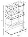
- FIG. 5is a perspective view of an electronic package, according to another embodiment of the invention, with a package substrate thereof shown in exploded form.
- An electronic package of the kind having a folded substrateis provided.
- the substrateis configured so that a stress concentration is created where folding is desired.
- the stress concentrationis created with first a resilient metal ground layer that resists bending and has an edge that promotes the creation of a stress concentration in a flexible layer at or near the edge.
- a second metal ground layerresists bending in another portion of the substrate, and also has an edge creating a stress concentration in a different area of the flexible layer.
- the portions of the substrate having the first and second resilient metal ground layerscan be folded over one another with substantially no bending in these portions, while a fold portion between the edges bends to allow for folding of the substrate. Bending of the fold portion is also promoted because the fold portion is not as thick as the portions having the resilient metal ground layers.
- Another embodimentmay make use of a different mechanism to create one or more stress concentrations.
- FIG. 1 of the accompanying drawingsillustrates components of an electronic package 10 , according to an embodiment of the invention, including various layers of a package substrate 12 before being folded, vias 14 formed in some layers of the package substrate 12 , first and second electronic devices 16 and 18 mounted to the package substrate 12 , and solder ball terminals 20 that are attached to the package substrate 12 .
- a core of the package substrate 12is a flexible layer 22 made of polyimide, an insulator.
- First and second thin metal layers 24 and 26are formed on upper and lower surfaces of the flexible layer 22 , respectively.
- the thin metal layers 24 and 26are initially uniformly formed over the length and width of the flexible layer 22 .
- the thin metal layers 24are then patterned so that areas are removed and other areas, including contacts 28 and traces 30 , remain behind.
- a first solder mask 32is formed over the remaining portions of the first thin metal layer 24 . Areas 34 of the first solder mask 32 are selectively removed in an etching process, to expose the contacts 28 of the first thin metal layer 24 .
- the combination of the flexible layer 22 , the first and second thin metal layers 24 and 26 , and the first solder mask 32is still relatively flexible and can be folded at any desired location.
- First and second resilient ground metal layers 36 and 38are then plated on select areas on a lower surface of the second thin metal layer 26 .
- the first and second resilient ground metal layers 36 and 38are in the same plane.
- the first resilient ground metal layer 36has a left edge 40 .
- the second resilient ground metal layer 38is plated to the left of the first resilient ground metal layer 36 and has a right edge 42 .
- the edges 40 and 42are in a parallel, spaced, and facing relationship relative to one another.
- the first and second ground metal layers 36 and 38rigidify portions of the package substrate 12 that they form part of, to resist bending of the portions that they form part of, while still allowing for folding of other portions of the package substrate 12 .
- a second solder mask 44is subsequently formed on lower surfaces of the first and second resilient ground metal layers 36 and 38 .
- the second solder mask 44is also formed on some exposed areas of the second thin metal layer 26 .
- the second solder mask 44is not formed on exposed areas of the second thin metal layer defined between the edges 40 and 42 .
- the solder ball terminals 20are attached to a lower side of the package substrate 12 , and the first and second electronic devices 16 and 18 are mounted to an upper surface of the package substrate 12 .
- the package substratecan generally be divided into first and second portions 48 and 50 , and a fold portion 52 between the first and second portions 48 and 50 .
- the first portion 48includes and extends up to the edge 40 of the first resilient ground metal layer 36 .
- the second portion 50includes and extends up to the edge 42 of the second resilient ground metal layer 38 .
- the fold portion 52extends from the edge 40 to the 42 .
- the electronic package 10is illustrated after the package substrate 12 is folded at the fold portion 52 .
- the second portion 50is then in a plane above and parallel to the first portion 48 .
- the first and second resilient ground metal layers 36 and 38resist bending or folding of the first and second portions 48 and 50 .
- the fold portion 52is, however, easily bent due to the absence of any resilient layers such as the first and second resilient ground metal layers 36 and 38 , and also because the fold portion 52 is not as thick as the first or second portions 48 or 50 .
- first and second resilient ground metal layersand in particular the edges 40 and 42 thereof, promote bending of the fold portion 52 from near the edge 40 to near the edge 42 .
- a desired portion of the substrate 12is thus bent, whereas other portions remain substantially flat.
- a stress concentration 53is created in the fold portion 52 near the edge 40 .
- the stress concentration 53is created because of the materials and geometry of the package substrate 12 in the region of the edge 40 .
- a similar stress concentrationis created in the fold portion near the edge 42 in FIG. 2 . It should, however, be understood that other mechanisms may be employed to create a stress concentration that controls bending of a substrate such that a fold portion thereof is bent, whereas other portions thereof remain substantially flat.
- the first and second electronic devices 16 and 18are microelectronic dies that include integrated circuits.
- Wirebonding wires 54connect respective ones of lands (not shown) on each of the electronic devices 16 and 18 to respective ones of the contacts 28 of the first thin metal layer 24 .
- the traces 30all extend from the first portion 48 through the fold portion 52 to the second portion 50 . Some of the traces 30 connect the second electronic device 18 to the first electronic device 16 . Other ones of the traces 30 connect the second electronic device 18 through contacts 28 in the first portion 48 and the vias 14 to the solder ball terminals 20 .
- the first electronic device 16is also connected through the contacts 28 in the first portion 48 and some of the vias 14 to the solder ball terminals 20 .
- signalscan be provided through the solder ball terminals 20 to and from either electronic device 16 or 18 , and that signals can be transmitted between the electronic devices 16 and 18 .
- Some of the vias 14are also formed in the first resilient ground metal layer 36 , and can be connected to either electronic device 16 or 18 .
- Some of the solder ball terminals 20are directly attached to the first resilient ground metal layer 36 , and can provide a ground or reference voltage through the first resilient ground metal layer 36 to the electronic devices 16 and 18 .
- ground planes 36 and 38for improved signal referencing and better controlled impedance.
- the substrate 12is still foldable due to selective placement of the ground planes 36 and 38 .
- FIG. 4illustrates how one of the vias 14 in the first resilient ground metal layer 36 is formed.
- a via opening 56is laser-drilled in the second thin metal layer 26 , and the flexible layer 22 .
- the via 14is plated in the via opening 56 when the first resilient ground metal layer 36 is plated on the second thin metal layer 26 .
- Other viasmay simultaneously be plated when the first resilient ground metal layer 36 is plated, but can be electrically isolated from the first resilient ground metal layer 36 for purposes of providing signals to or from the electronic devices 16 or 18 .
- the electronic devices 16 and 18are mounted on the same side of the unfolded package substrate 12 . As illustrated in FIG. 2 , the electronic devices 16 and 18 are both on the inside of the folded package substrate 12 .
- electronic devices 16 A and 18 Amay be mounted on opposing sides of an unfolded package substrate 12 A.
- the package substrate 12 Amay have first and second resilient ground metal layers 36 A and 38 A.
- the second resilient ground metal layer 38 Amay have a routing opening 60 .
- Wirebonding wires 54 Amay extend from the second electronic devices 18 A through the routing opening 60 and openings in a second thin metal layer 26 and a flexible layer 22 to contacts 28 of a first thin metal layer 24 .
- the package substrate 12 Athus includes a first portion including the first resilient ground metal layer 36 A, a second portion including the second resilient ground metal layer 38 A, and a fold portion between the first and second resilient ground metal layers 36 A and 38 A.
- Folding of the package substrate 12 A in a direction 62will place the first electronic device 16 A on top of the first portion that includes the first resilient ground metal layer 36 A, and the second electronic device 18 A will be placed on top of the second portion that includes the second resilient ground metal layer 38 A.
Landscapes
- Engineering & Computer Science (AREA)
- Microelectronics & Electronic Packaging (AREA)
- Physics & Mathematics (AREA)
- Condensed Matter Physics & Semiconductors (AREA)
- General Physics & Mathematics (AREA)
- Computer Hardware Design (AREA)
- Power Engineering (AREA)
- Structure Of Printed Boards (AREA)
Abstract
Description
1). Field of the Invention
This invention relates to an electronic package having a folded, flexible substrate, and to a method of constructing such an electronic package.
2). Discussion of Related Art
Integrated circuits are usually manufactured on semiconductor wafers that are subsequently singulated into individual dies. Such a die may be extremely thin, often less than 100 microns, and is subsequently mounted to a package substrate for purposes of structural integrity. The package substrate also has conductors in the form of traces thereon, metal lines therein, and/or vias therein to provide electric interconnection to other devices, often other integrated circuits or other dies.
In order to save space in x and y, it is often required to stack more than one die on top of one another in a z-direction, with the integrated circuits of the dies interconnected with one another. Two dies can, for example, be mounted to a flexible package substrate, and the flexible package substrate be folded into positions such that the dies are above one another.
A package substrate of the aforementioned kind is usually uniformly flexible across its width. When one portion of the package substrate is folded over another portion of the package substrate, a fold region may be created at an undesired, even arbitrary area of the package substrate. Folding of the substrate at undesired areas may cause damage to certain components of the substrate. Bending at arbitrary locations may cause inconsistencies in bending from one assembly to the next, which may result in incorrect downstream packaging. Uncontrolled folding may also result in an undesired form factor of the final electronic package.
The invention is described by way of example with reference to the accompanying drawings, wherein:
An electronic package of the kind having a folded substrate is provided. The substrate is configured so that a stress concentration is created where folding is desired. In the present example, the stress concentration is created with first a resilient metal ground layer that resists bending and has an edge that promotes the creation of a stress concentration in a flexible layer at or near the edge. A second metal ground layer resists bending in another portion of the substrate, and also has an edge creating a stress concentration in a different area of the flexible layer. The portions of the substrate having the first and second resilient metal ground layers can be folded over one another with substantially no bending in these portions, while a fold portion between the edges bends to allow for folding of the substrate. Bending of the fold portion is also promoted because the fold portion is not as thick as the portions having the resilient metal ground layers. Another embodiment may make use of a different mechanism to create one or more stress concentrations.
Resilient Metal Ground Planes for Controlled Folding
A core of thepackage substrate 12 is aflexible layer 22 made of polyimide, an insulator. First and secondthin metal layers flexible layer 22, respectively. Thethin metal layers flexible layer 22. Thethin metal layers 24 are then patterned so that areas are removed and other areas, includingcontacts 28 and traces30, remain behind.
Afirst solder mask 32 is formed over the remaining portions of the firstthin metal layer 24.Areas 34 of thefirst solder mask 32 are selectively removed in an etching process, to expose thecontacts 28 of the firstthin metal layer 24. The combination of theflexible layer 22, the first and secondthin metal layers first solder mask 32 is still relatively flexible and can be folded at any desired location.
First and second resilientground metal layers thin metal layer 26. The first and second resilientground metal layers ground metal layer 36 has aleft edge 40. The second resilientground metal layer 38 is plated to the left of the first resilientground metal layer 36 and has aright edge 42. Theedges ground metal layers package substrate 12 that they form part of, to resist bending of the portions that they form part of, while still allowing for folding of other portions of thepackage substrate 12.
Asecond solder mask 44 is subsequently formed on lower surfaces of the first and second resilientground metal layers second solder mask 44 is also formed on some exposed areas of the secondthin metal layer 26. In the present example, thesecond solder mask 44 is not formed on exposed areas of the second thin metal layer defined between theedges
Thesolder ball terminals 20 are attached to a lower side of thepackage substrate 12, and the first and secondelectronic devices package substrate 12.
Reference is now made toFIG. 2 . The package substrate can generally be divided into first andsecond portions fold portion 52 between the first andsecond portions first portion 48 includes and extends up to theedge 40 of the first resilientground metal layer 36. Thesecond portion 50 includes and extends up to theedge 42 of the second resilientground metal layer 38. Thefold portion 52 extends from theedge 40 to the42.
Theelectronic package 10 is illustrated after thepackage substrate 12 is folded at thefold portion 52. Thesecond portion 50 is then in a plane above and parallel to thefirst portion 48. What should be noted is that the first and second resilientground metal layers second portions fold portion 52 is, however, easily bent due to the absence of any resilient layers such as the first and second resilientground metal layers fold portion 52 is not as thick as the first orsecond portions
It can thus be said that the first and second resilient ground metal layers, and in particular theedges fold portion 52 from near theedge 40 to near theedge 42. A desired portion of thesubstrate 12 is thus bent, whereas other portions remain substantially flat.
As illustrated inFIG. 3 , astress concentration 53 is created in thefold portion 52 near theedge 40. Thestress concentration 53 is created because of the materials and geometry of thepackage substrate 12 in the region of theedge 40. A similar stress concentration is created in the fold portion near theedge 42 inFIG. 2 . It should, however, be understood that other mechanisms may be employed to create a stress concentration that controls bending of a substrate such that a fold portion thereof is bent, whereas other portions thereof remain substantially flat.
Electric Interconnection
The first and secondelectronic devices Wirebonding wires 54 connect respective ones of lands (not shown) on each of theelectronic devices contacts 28 of the firstthin metal layer 24. Thetraces 30 all extend from thefirst portion 48 through thefold portion 52 to thesecond portion 50. Some of thetraces 30 connect the secondelectronic device 18 to the firstelectronic device 16. Other ones of thetraces 30 connect the secondelectronic device 18 throughcontacts 28 in thefirst portion 48 and the vias14 to thesolder ball terminals 20. The firstelectronic device 16 is also connected through thecontacts 28 in thefirst portion 48 and some of the vias14 to thesolder ball terminals 20.
It can thus be seen that signals can be provided through thesolder ball terminals 20 to and from eitherelectronic device electronic devices vias 14 are also formed in the first resilientground metal layer 36, and can be connected to eitherelectronic device solder ball terminals 20 are directly attached to the first resilientground metal layer 36, and can provide a ground or reference voltage through the first resilientground metal layer 36 to theelectronic devices
What is thus provided is a substrate which includes ground planes36 and38 for improved signal referencing and better controlled impedance. What should be noted is that although the ground planes36 and38 are relatively resilient, thesubstrate 12 is still foldable due to selective placement of the ground planes36 and38.
Alternative Embodiment
In the embodiment ofFIG. 1 , theelectronic devices package substrate 12. As illustrated inFIG. 2 , theelectronic devices package substrate 12.
As illustrated inFIG. 5 ,electronic devices package substrate 12A. As with the embodiment ofFIG. 1 , thepackage substrate 12A may have first and second resilientground metal layers 36A and38A. The second resilient ground metal layer38A may have arouting opening 60.Wirebonding wires 54A may extend from the secondelectronic devices 18A through therouting opening 60 and openings in a secondthin metal layer 26 and aflexible layer 22 tocontacts 28 of a firstthin metal layer 24.
Like reference numerals used inFIGS. 1 and 5 indicate like components, and it should thus be evident that thepackage substrate 12A is the same as thepackage substrate 12 in all other respects. Thepackage substrate 12A thus includes a first portion including the first resilientground metal layer 36A, a second portion including the second resilient ground metal layer38A, and a fold portion between the first and second resilientground metal layers 36A and38A.
Folding of thepackage substrate 12A in adirection 62 will place the firstelectronic device 16A on top of the first portion that includes the first resilientground metal layer 36A, and the secondelectronic device 18A will be placed on top of the second portion that includes the second resilient ground metal layer38A.
While certain exemplary embodiments have been described and shown in the accompanying drawings, it is to be understood that such embodiments are merely illustrative and not restrictive of the current invention, and that this invention is not restricted to the specific constructions and arrangements shown and described since modifications may occur to those ordinarily skilled in the art. For example, although reference is made to “metal,” it should be understood that other conductive materials may be used instead of metal with similar effect.
Claims (15)
1. An electronic package, comprising:
a substrate having at least (i) a first resilient layer, (ii) a second resilient layer in a plane parallel to and above the first resilient layer, the first and second resilient layers respectively having first and second substantially parallel spaced edges, and (iii) a flexible layer which is bent, with the first and second edges promoting where the flexible layer is bent;
a plurality of traces supported by the substrate and extending from a first portion to a second portion on respectively first and second opposite sides of the edge; and
at least a first electronic device, carrying an integrated circuit, mounted to the substrate on the first side of the edge.
2. The electronic package ofclaim 1 , further comprising:
a second electronic device mounted to the substrate on the second side of the edge.
3. An electronic package, comprising:
a substrate having a first portion, a second portion, and a fold portion between the first and second portions, the substrate including at least a first resilient layer forming part of the first portion and a flexible layer, the flexible layer being bent so that the second portion is in a plane above and substantially parallel to the first portion, with a first edge of the first resilient layer promoting where the flexible layer is bent;
a plurality of first contacts exposed on an upper side of the first portion;
a plurality of terminals exposed on a lower side of the first portion;
a plurality of vias in the first portion interconnecting at least some of the first contacts with at least some of the terminals;
a plurality of second exposed contacts on the second portion; and
a plurality of traces supported by the substrate and extending from the first portion across the fold portion to the second portion to the second contacts.
4. The electronic package ofclaim 3 , wherein the substrate includes a second resilient layer forming part of the second portion, a second edge of the second portion promoting where the flexible layer is bent, the fold region being between the first and second edges.
5. The electronic package ofclaim 4 , wherein the edges create stress concentrations in the fold portion of the flexible layer.
6. The electronic package ofclaim 3 , wherein at least one of the traces interconnects one of the first contacts with one of the second contacts.
7. The electronic package ofclaim 6 , wherein at least one of the traces interconnects one of the terminals with one of the second contacts.
8. The electronic package ofclaim 3 , wherein at least one of the traces interconnects one of the terminals with one of the second contacts.
9. The electronic package ofclaim 3 , wherein the first resilient layer is made of metal.
10. The electronic package ofclaim 9 , wherein the first resilient layer is electrically connected to one of the terminals.
11. The electronic package ofclaim 3 , further comprising:
at least a first electronic device, carrying an integrated circuit, mounted to the first portion and having lands that are electrically connected to the first contacts.
12. The electronic package ofclaim 11 , further comprising:
at least a second electronic device, carrying an integrated circuit, mounted to the second portion and having lands that are electrically connected to the second contacts.
13. An electronic package, comprising:
a substrate having a first portion, a second portion, and a fold portion between the first and second portions, the substrate including at least a first resilient layer forming part of the first portion, a second resilient layer forming part of the second portion, and a flexible layer, the flexible layer being bent so that the second portion is in a plane above and substantially parallel to the first portion, with a first edge of the first resilient layer promoting where the flexible layer is bent and a second edge of the second portion promoting where the flexible layer is bent, the fold region being between the first and second edges;
a plurality of first contacts exposed on an upper side of the first portion;
at least a first electronic device, carrying an integrated circuit, mounted to the first portion and having lands that are electrically connected to the first contacts.
a plurality of terminals exposed on a lower side of the first portion;
a plurality of vias in the first portion interconnecting at least some of the first contacts with at least some of the terminals;
a plurality of second exposed contacts on the second portion;
at least a second electronic device, carrying an integrated circuit, mounted to the second portion and having lands that are electrically connected to the second contacts; and
a plurality of traces supported by the substrate and extending from the first portion across the fold portion to the second portion to the second contacts.
14. The electronic package ofclaim 13 , wherein the first resilient layer is made of metal.
15. The electronic package ofclaim 14 , wherein the first resilient layer is electrically connected to one of the terminals.
Priority Applications (2)
| Application Number | Priority Date | Filing Date | Title |
|---|---|---|---|
| US10/623,073US6992376B2 (en) | 2003-07-17 | 2003-07-17 | Electronic package having a folded package substrate |
| US11/270,936US7563645B2 (en) | 2003-07-17 | 2005-11-10 | Electronic package having a folded package substrate |
Applications Claiming Priority (1)
| Application Number | Priority Date | Filing Date | Title |
|---|---|---|---|
| US10/623,073US6992376B2 (en) | 2003-07-17 | 2003-07-17 | Electronic package having a folded package substrate |
Related Child Applications (1)
| Application Number | Title | Priority Date | Filing Date |
|---|---|---|---|
| US11/270,936DivisionUS7563645B2 (en) | 2003-07-17 | 2005-11-10 | Electronic package having a folded package substrate |
Publications (2)
| Publication Number | Publication Date |
|---|---|
| US20050012194A1 US20050012194A1 (en) | 2005-01-20 |
| US6992376B2true US6992376B2 (en) | 2006-01-31 |
Family
ID=34063298
Family Applications (2)
| Application Number | Title | Priority Date | Filing Date |
|---|---|---|---|
| US10/623,073Expired - LifetimeUS6992376B2 (en) | 2003-07-17 | 2003-07-17 | Electronic package having a folded package substrate |
| US11/270,936Expired - LifetimeUS7563645B2 (en) | 2003-07-17 | 2005-11-10 | Electronic package having a folded package substrate |
Family Applications After (1)
| Application Number | Title | Priority Date | Filing Date |
|---|---|---|---|
| US11/270,936Expired - LifetimeUS7563645B2 (en) | 2003-07-17 | 2005-11-10 | Electronic package having a folded package substrate |
Country Status (1)
| Country | Link |
|---|---|
| US (2) | US6992376B2 (en) |
Cited By (49)
| Publication number | Priority date | Publication date | Assignee | Title |
|---|---|---|---|---|
| US20070215378A1 (en)* | 2006-03-14 | 2007-09-20 | Funai Electric Co., Ltd. | Circuit board |
| US20080122113A1 (en)* | 2006-08-17 | 2008-05-29 | Corisis David J | Semiconductor device assemblies and systems including at least one conductive pathway extending around a side of at least one semiconductor device and methods for forming the same |
| US20080218974A1 (en)* | 2007-03-06 | 2008-09-11 | Gerald Keith Bartley | Method and Structure for Connecting, Stacking, and Cooling Chips on a Flexible Carrier |
| US20090032289A1 (en)* | 2007-07-31 | 2009-02-05 | Nokia Corporation | Circuit board having two or more planar sections |
| US20100244243A1 (en)* | 2009-03-24 | 2010-09-30 | Kabushiki Kaisha Toshiba | Semiconductor device |
| US20120061846A1 (en)* | 2009-06-02 | 2012-03-15 | Hsio Technologies, Llc | Compliant printed circuit area array semiconductor device package |
| US8753762B2 (en) | 2011-03-03 | 2014-06-17 | Chrysler Group Llc | Thermal management of cabin and battery pack in HEV/PHEV/BEV vehicles |
| US8789272B2 (en) | 2009-06-02 | 2014-07-29 | Hsio Technologies, Llc | Method of making a compliant printed circuit peripheral lead semiconductor test socket |
| US8803539B2 (en) | 2009-06-03 | 2014-08-12 | Hsio Technologies, Llc | Compliant wafer level probe assembly |
| US8912812B2 (en) | 2009-06-02 | 2014-12-16 | Hsio Technologies, Llc | Compliant printed circuit wafer probe diagnostic tool |
| US8928344B2 (en) | 2009-06-02 | 2015-01-06 | Hsio Technologies, Llc | Compliant printed circuit socket diagnostic tool |
| US8955215B2 (en) | 2009-05-28 | 2015-02-17 | Hsio Technologies, Llc | High performance surface mount electrical interconnect |
| US8955216B2 (en) | 2009-06-02 | 2015-02-17 | Hsio Technologies, Llc | Method of making a compliant printed circuit peripheral lead semiconductor package |
| US8970031B2 (en) | 2009-06-16 | 2015-03-03 | Hsio Technologies, Llc | Semiconductor die terminal |
| US8981809B2 (en) | 2009-06-29 | 2015-03-17 | Hsio Technologies, Llc | Compliant printed circuit semiconductor tester interface |
| US8981568B2 (en) | 2009-06-16 | 2015-03-17 | Hsio Technologies, Llc | Simulated wirebond semiconductor package |
| US8988093B2 (en) | 2009-06-02 | 2015-03-24 | Hsio Technologies, Llc | Bumped semiconductor wafer or die level electrical interconnect |
| US8987886B2 (en) | 2009-06-02 | 2015-03-24 | Hsio Technologies, Llc | Copper pillar full metal via electrical circuit structure |
| US8984748B2 (en) | 2009-06-29 | 2015-03-24 | Hsio Technologies, Llc | Singulated semiconductor device separable electrical interconnect |
| US9076884B2 (en) | 2009-06-02 | 2015-07-07 | Hsio Technologies, Llc | Compliant printed circuit semiconductor package |
| US9093767B2 (en) | 2009-06-02 | 2015-07-28 | Hsio Technologies, Llc | High performance surface mount electrical interconnect |
| US9136196B2 (en) | 2009-06-02 | 2015-09-15 | Hsio Technologies, Llc | Compliant printed circuit wafer level semiconductor package |
| US9184527B2 (en) | 2009-06-02 | 2015-11-10 | Hsio Technologies, Llc | Electrical connector insulator housing |
| US9184145B2 (en) | 2009-06-02 | 2015-11-10 | Hsio Technologies, Llc | Semiconductor device package adapter |
| US9231328B2 (en) | 2009-06-02 | 2016-01-05 | Hsio Technologies, Llc | Resilient conductive electrical interconnect |
| US9232654B2 (en) | 2009-06-02 | 2016-01-05 | Hsio Technologies, Llc | High performance electrical circuit structure |
| US9276336B2 (en) | 2009-05-28 | 2016-03-01 | Hsio Technologies, Llc | Metalized pad to electrical contact interface |
| US9276339B2 (en) | 2009-06-02 | 2016-03-01 | Hsio Technologies, Llc | Electrical interconnect IC device socket |
| US9277654B2 (en) | 2009-06-02 | 2016-03-01 | Hsio Technologies, Llc | Composite polymer-metal electrical contacts |
| US9320144B2 (en) | 2009-06-17 | 2016-04-19 | Hsio Technologies, Llc | Method of forming a semiconductor socket |
| US9318862B2 (en) | 2009-06-02 | 2016-04-19 | Hsio Technologies, Llc | Method of making an electronic interconnect |
| US9320133B2 (en) | 2009-06-02 | 2016-04-19 | Hsio Technologies, Llc | Electrical interconnect IC device socket |
| US9350093B2 (en) | 2010-06-03 | 2016-05-24 | Hsio Technologies, Llc | Selective metalization of electrical connector or socket housing |
| US9414500B2 (en) | 2009-06-02 | 2016-08-09 | Hsio Technologies, Llc | Compliant printed flexible circuit |
| US9439326B1 (en)* | 2015-05-28 | 2016-09-06 | Hana Micron, Inc. | Electronic components |
| US20160353564A1 (en)* | 2014-11-27 | 2016-12-01 | Shenzhen China Star Optoelectronics Technology Co. Ltd. | L-Bending PCB |
| US9536815B2 (en) | 2009-05-28 | 2017-01-03 | Hsio Technologies, Llc | Semiconductor socket with direct selective metalization |
| US9559447B2 (en) | 2015-03-18 | 2017-01-31 | Hsio Technologies, Llc | Mechanical contact retention within an electrical connector |
| US9613841B2 (en) | 2009-06-02 | 2017-04-04 | Hsio Technologies, Llc | Area array semiconductor device package interconnect structure with optional package-to-package or flexible circuit to package connection |
| US9689897B2 (en) | 2010-06-03 | 2017-06-27 | Hsio Technologies, Llc | Performance enhanced semiconductor socket |
| US9699906B2 (en) | 2009-06-02 | 2017-07-04 | Hsio Technologies, Llc | Hybrid printed circuit assembly with low density main core and embedded high density circuit regions |
| US9761520B2 (en) | 2012-07-10 | 2017-09-12 | Hsio Technologies, Llc | Method of making an electrical connector having electrodeposited terminals |
| US9930775B2 (en) | 2009-06-02 | 2018-03-27 | Hsio Technologies, Llc | Copper pillar full metal via electrical circuit structure |
| US10159154B2 (en) | 2010-06-03 | 2018-12-18 | Hsio Technologies, Llc | Fusion bonded liquid crystal polymer circuit structure |
| US10170449B2 (en) | 2017-05-02 | 2019-01-01 | International Business Machines Corporation | Deformable closed-loop multi-layered microelectronic device |
| US10483254B2 (en) | 2017-01-17 | 2019-11-19 | Advanced Semiconductor Engineering, Inc. | Electronic module and semiconductor package device |
| US10506722B2 (en) | 2013-07-11 | 2019-12-10 | Hsio Technologies, Llc | Fusion bonded liquid crystal polymer electrical circuit structure |
| US10667410B2 (en) | 2013-07-11 | 2020-05-26 | Hsio Technologies, Llc | Method of making a fusion bonded circuit structure |
| US11050207B2 (en)* | 2015-04-08 | 2021-06-29 | Securitag Assembly Group Co., Ltd. | Crimping apparatus and system for crimping a flexible printed circuit |
Families Citing this family (18)
| Publication number | Priority date | Publication date | Assignee | Title |
|---|---|---|---|---|
| KR100699823B1 (en)* | 2003-08-05 | 2007-03-27 | 삼성전자주식회사 | Low Cost Flexible Film Package Module and Manufacturing Method Thereof |
| US7154175B2 (en)* | 2004-06-21 | 2006-12-26 | Intel Corporation | Ground plane for integrated circuit package |
| DE102005003369A1 (en)* | 2005-01-24 | 2006-07-27 | Juma Pcb Gmbh | Method for producing a spatial printed circuit board structure comprising at least two printed circuit board sections arranged at an angle to one another |
| US20060278962A1 (en)* | 2005-06-09 | 2006-12-14 | Tessera, Inc. | Microelectronic loop packages |
| US20100155863A1 (en)* | 2005-08-11 | 2010-06-24 | Koninklijke Philips Electronics, N.V. | Method for manufacturing a microelectronic package comprising a silicon mems microphone |
| US7767543B2 (en)* | 2005-09-06 | 2010-08-03 | Semiconductor Energy Laboratory Co., Ltd. | Method for manufacturing a micro-electro-mechanical device with a folded substrate |
| US7425758B2 (en)* | 2006-08-28 | 2008-09-16 | Micron Technology, Inc. | Metal core foldover package structures |
| JP2009164160A (en)* | 2007-12-28 | 2009-07-23 | Panasonic Corp | Semiconductor device laminate and mounting method |
| WO2010029611A1 (en)* | 2008-09-09 | 2010-03-18 | 富士通株式会社 | Multilayer flexible printed wiring board and electronic device |
| US7874848B2 (en)* | 2008-10-06 | 2011-01-25 | Hitachi Chemical Company, Ltd. | Connector for inserting wiring board, and method for manufacturing the same |
| US8217507B1 (en)* | 2010-01-22 | 2012-07-10 | Amkor Technology, Inc. | Edge mount semiconductor package |
| WO2013109947A1 (en)* | 2012-01-19 | 2013-07-25 | Nike International Ltd. | Wearable device assembly having solder mask |
| JP6258290B2 (en)* | 2013-02-26 | 2018-01-10 | タツタ電線株式会社 | Reinforcing member for flexible printed wiring board, flexible printed wiring board, and shield printed wiring board |
| CN204884440U (en)* | 2015-08-27 | 2015-12-16 | 京东方科技集团股份有限公司 | Flexible display panel and flexible display device |
| US10014710B2 (en)* | 2015-12-09 | 2018-07-03 | Intel Corporation | Foldable fabric-based packaging solution |
| US10388636B2 (en)* | 2015-12-21 | 2019-08-20 | Intel Corporation | Integrating system in package (SIP) with input/output (IO) board for platform miniaturization |
| CN108962035B (en)* | 2018-08-02 | 2020-11-06 | 京东方科技集团股份有限公司 | Flexible display device |
| CN110010593B (en)* | 2018-10-10 | 2020-09-29 | 浙江集迈科微电子有限公司 | Three-dimensional stacked system-in-package process |
Citations (25)
| Publication number | Priority date | Publication date | Assignee | Title |
|---|---|---|---|---|
| US5639990A (en)* | 1992-06-05 | 1997-06-17 | Mitsui Toatsu Chemicals, Inc. | Solid printed substrate and electronic circuit package using the same |
| US5776797A (en)* | 1995-12-22 | 1998-07-07 | Fairchild Space And Defense Corporation | Three-dimensional flexible assembly of integrated circuits |
| US6121676A (en)* | 1996-12-13 | 2000-09-19 | Tessera, Inc. | Stacked microelectronic assembly and method therefor |
| US6225688B1 (en)* | 1997-12-11 | 2001-05-01 | Tessera, Inc. | Stacked microelectronic assembly and method therefor |
| US6300679B1 (en)* | 1998-06-01 | 2001-10-09 | Semiconductor Components Industries, Llc | Flexible substrate for packaging a semiconductor component |
| US20010040793A1 (en)* | 2000-02-01 | 2001-11-15 | Tetsuya Inaba | Electronic device and method of producing the same |
| US6376769B1 (en)* | 1999-05-18 | 2002-04-23 | Amerasia International Technology, Inc. | High-density electronic package, and method for making same |
| US20020114143A1 (en)* | 2000-12-28 | 2002-08-22 | Morrison Gary P. | Chip-scale packages stacked on folded interconnector for vertical assembly on substrates |
| US6444921B1 (en)* | 2000-02-03 | 2002-09-03 | Fujitsu Limited | Reduced stress and zero stress interposers for integrated-circuit chips, multichip substrates, and the like |
| US20020125044A1 (en)* | 2000-12-28 | 2002-09-12 | Henry Johnson | Layered circuit boards and methods of production thereof |
| US20020164838A1 (en)* | 2001-05-02 | 2002-11-07 | Moon Ow Chee | Flexible ball grid array chip scale packages and methods of fabrication |
| US20030067064A1 (en)* | 2001-10-10 | 2003-04-10 | Shin Kim | Stack package using flexible double wiring substrate |
| US6563223B2 (en)* | 2000-08-22 | 2003-05-13 | Micron Technology, Inc. | Interconnection component for facilitating testing of packaged integrated circuits |
| JP2003197693A (en)* | 2001-12-28 | 2003-07-11 | Suzuki Co Ltd | Apparatus and method for implanting film carrier tape for mounting electronic element, and method for manufacturing the film carrier tape |
| US6600222B1 (en)* | 2002-07-17 | 2003-07-29 | Intel Corporation | Stacked microelectronic packages |
| US20040097086A1 (en)* | 2002-09-26 | 2004-05-20 | Yusuke Igarashi | Method for manufacturing circuit devices |
| US20040115866A1 (en)* | 2002-09-06 | 2004-06-17 | Tessera, Inc. | Methods of making microelectronic packages including folded substrates |
| US20040113275A1 (en)* | 2002-10-08 | 2004-06-17 | Chippac, Inc. | Semiconductor multi-package module having inverted second package stacked over die-up flip-chip ball grid array (BGA) package |
| US20040124527A1 (en)* | 2002-12-31 | 2004-07-01 | Chia-Pin Chiu | Folded BGA package design with shortened communication paths and more electrical routing flexibility |
| US6770813B1 (en)* | 2003-05-16 | 2004-08-03 | Visteon Global Technologies, Inc. | Mountable microelectronic package |
| US6785144B1 (en)* | 1999-06-10 | 2004-08-31 | Micron Technology, Inc. | High density stackable and flexible substrate-based devices and systems and methods of fabricating |
| US20040218848A1 (en)* | 2003-04-30 | 2004-11-04 | Industrial Technology Research Institute | Flexible electronic/optical interconnection film assembly and method for manufacturing |
| US20040238936A1 (en)* | 2003-05-28 | 2004-12-02 | Rumer Christopher L. | Through silicon via, folded flex microelectronic package |
| US20040264148A1 (en)* | 2003-06-27 | 2004-12-30 | Burdick William Edward | Method and system for fan fold packaging |
| US6890186B2 (en)* | 2000-12-01 | 2005-05-10 | Via Technologies, Inc. | Socket structure for grid array (GA) packages |
Family Cites Families (5)
| Publication number | Priority date | Publication date | Assignee | Title |
|---|---|---|---|---|
| US4834660A (en)* | 1987-06-03 | 1989-05-30 | Harris Corporation | Flexible zero insertion force interconnector between circuit boards |
| US5224023A (en)* | 1992-02-10 | 1993-06-29 | Smith Gary W | Foldable electronic assembly module |
| US5436744A (en)* | 1993-09-03 | 1995-07-25 | Motorola Inc. | Flexible liquid crystal display with integrated driver circuit and display electrodes formed on opposite sides of folded substrate |
| US6136468A (en)* | 1998-08-25 | 2000-10-24 | Timer Technologies, Llc | Electrochemical cell with deferred assembly |
| AU6349000A (en)* | 1999-07-16 | 2001-02-05 | Silicon Film Technologies, Inc. | High-density packaging of integrated circuits |
- 2003
- 2003-07-17USUS10/623,073patent/US6992376B2/ennot_activeExpired - Lifetime
- 2005
- 2005-11-10USUS11/270,936patent/US7563645B2/ennot_activeExpired - Lifetime
Patent Citations (28)
| Publication number | Priority date | Publication date | Assignee | Title |
|---|---|---|---|---|
| US5639990A (en)* | 1992-06-05 | 1997-06-17 | Mitsui Toatsu Chemicals, Inc. | Solid printed substrate and electronic circuit package using the same |
| US5776797A (en)* | 1995-12-22 | 1998-07-07 | Fairchild Space And Defense Corporation | Three-dimensional flexible assembly of integrated circuits |
| US6121676A (en)* | 1996-12-13 | 2000-09-19 | Tessera, Inc. | Stacked microelectronic assembly and method therefor |
| US6699730B2 (en)* | 1996-12-13 | 2004-03-02 | Tessers, Inc. | Stacked microelectronic assembly and method therefor |
| US6225688B1 (en)* | 1997-12-11 | 2001-05-01 | Tessera, Inc. | Stacked microelectronic assembly and method therefor |
| US6300679B1 (en)* | 1998-06-01 | 2001-10-09 | Semiconductor Components Industries, Llc | Flexible substrate for packaging a semiconductor component |
| US6376769B1 (en)* | 1999-05-18 | 2002-04-23 | Amerasia International Technology, Inc. | High-density electronic package, and method for making same |
| US6785144B1 (en)* | 1999-06-10 | 2004-08-31 | Micron Technology, Inc. | High density stackable and flexible substrate-based devices and systems and methods of fabricating |
| US20010040793A1 (en)* | 2000-02-01 | 2001-11-15 | Tetsuya Inaba | Electronic device and method of producing the same |
| US6444921B1 (en)* | 2000-02-03 | 2002-09-03 | Fujitsu Limited | Reduced stress and zero stress interposers for integrated-circuit chips, multichip substrates, and the like |
| US6563223B2 (en)* | 2000-08-22 | 2003-05-13 | Micron Technology, Inc. | Interconnection component for facilitating testing of packaged integrated circuits |
| US6890186B2 (en)* | 2000-12-01 | 2005-05-10 | Via Technologies, Inc. | Socket structure for grid array (GA) packages |
| US20020114143A1 (en)* | 2000-12-28 | 2002-08-22 | Morrison Gary P. | Chip-scale packages stacked on folded interconnector for vertical assembly on substrates |
| US20020125044A1 (en)* | 2000-12-28 | 2002-09-12 | Henry Johnson | Layered circuit boards and methods of production thereof |
| US20020164838A1 (en)* | 2001-05-02 | 2002-11-07 | Moon Ow Chee | Flexible ball grid array chip scale packages and methods of fabrication |
| US20030067064A1 (en)* | 2001-10-10 | 2003-04-10 | Shin Kim | Stack package using flexible double wiring substrate |
| JP2003197693A (en)* | 2001-12-28 | 2003-07-11 | Suzuki Co Ltd | Apparatus and method for implanting film carrier tape for mounting electronic element, and method for manufacturing the film carrier tape |
| US6600222B1 (en)* | 2002-07-17 | 2003-07-29 | Intel Corporation | Stacked microelectronic packages |
| US20040115866A1 (en)* | 2002-09-06 | 2004-06-17 | Tessera, Inc. | Methods of making microelectronic packages including folded substrates |
| US20040097086A1 (en)* | 2002-09-26 | 2004-05-20 | Yusuke Igarashi | Method for manufacturing circuit devices |
| US20040113275A1 (en)* | 2002-10-08 | 2004-06-17 | Chippac, Inc. | Semiconductor multi-package module having inverted second package stacked over die-up flip-chip ball grid array (BGA) package |
| US20040124527A1 (en)* | 2002-12-31 | 2004-07-01 | Chia-Pin Chiu | Folded BGA package design with shortened communication paths and more electrical routing flexibility |
| US6869825B2 (en)* | 2002-12-31 | 2005-03-22 | Intel Corporation | Folded BGA package design with shortened communication paths and more electrical routing flexibility |
| US20040218848A1 (en)* | 2003-04-30 | 2004-11-04 | Industrial Technology Research Institute | Flexible electronic/optical interconnection film assembly and method for manufacturing |
| US6770813B1 (en)* | 2003-05-16 | 2004-08-03 | Visteon Global Technologies, Inc. | Mountable microelectronic package |
| US20040238936A1 (en)* | 2003-05-28 | 2004-12-02 | Rumer Christopher L. | Through silicon via, folded flex microelectronic package |
| US6924551B2 (en)* | 2003-05-28 | 2005-08-02 | Intel Corporation | Through silicon via, folded flex microelectronic package |
| US20040264148A1 (en)* | 2003-06-27 | 2004-12-30 | Burdick William Edward | Method and system for fan fold packaging |
Cited By (58)
| Publication number | Priority date | Publication date | Assignee | Title |
|---|---|---|---|---|
| US20070215378A1 (en)* | 2006-03-14 | 2007-09-20 | Funai Electric Co., Ltd. | Circuit board |
| US20080122113A1 (en)* | 2006-08-17 | 2008-05-29 | Corisis David J | Semiconductor device assemblies and systems including at least one conductive pathway extending around a side of at least one semiconductor device and methods for forming the same |
| US7888185B2 (en)* | 2006-08-17 | 2011-02-15 | Micron Technology, Inc. | Semiconductor device assemblies and systems including at least one conductive pathway extending around a side of at least one semiconductor device |
| US20080218974A1 (en)* | 2007-03-06 | 2008-09-11 | Gerald Keith Bartley | Method and Structure for Connecting, Stacking, and Cooling Chips on a Flexible Carrier |
| US7675164B2 (en) | 2007-03-06 | 2010-03-09 | International Business Machines Corporation | Method and structure for connecting, stacking, and cooling chips on a flexible carrier |
| US20090032289A1 (en)* | 2007-07-31 | 2009-02-05 | Nokia Corporation | Circuit board having two or more planar sections |
| US20100244243A1 (en)* | 2009-03-24 | 2010-09-30 | Kabushiki Kaisha Toshiba | Semiconductor device |
| US8955215B2 (en) | 2009-05-28 | 2015-02-17 | Hsio Technologies, Llc | High performance surface mount electrical interconnect |
| US9660368B2 (en) | 2009-05-28 | 2017-05-23 | Hsio Technologies, Llc | High performance surface mount electrical interconnect |
| US9536815B2 (en) | 2009-05-28 | 2017-01-03 | Hsio Technologies, Llc | Semiconductor socket with direct selective metalization |
| US9276336B2 (en) | 2009-05-28 | 2016-03-01 | Hsio Technologies, Llc | Metalized pad to electrical contact interface |
| US9231328B2 (en) | 2009-06-02 | 2016-01-05 | Hsio Technologies, Llc | Resilient conductive electrical interconnect |
| US9320133B2 (en) | 2009-06-02 | 2016-04-19 | Hsio Technologies, Llc | Electrical interconnect IC device socket |
| US8912812B2 (en) | 2009-06-02 | 2014-12-16 | Hsio Technologies, Llc | Compliant printed circuit wafer probe diagnostic tool |
| US8955216B2 (en) | 2009-06-02 | 2015-02-17 | Hsio Technologies, Llc | Method of making a compliant printed circuit peripheral lead semiconductor package |
| US10609819B2 (en) | 2009-06-02 | 2020-03-31 | Hsio Technologies, Llc | Hybrid printed circuit assembly with low density main core and embedded high density circuit regions |
| US9930775B2 (en) | 2009-06-02 | 2018-03-27 | Hsio Technologies, Llc | Copper pillar full metal via electrical circuit structure |
| US9699906B2 (en) | 2009-06-02 | 2017-07-04 | Hsio Technologies, Llc | Hybrid printed circuit assembly with low density main core and embedded high density circuit regions |
| US8988093B2 (en) | 2009-06-02 | 2015-03-24 | Hsio Technologies, Llc | Bumped semiconductor wafer or die level electrical interconnect |
| US8987886B2 (en) | 2009-06-02 | 2015-03-24 | Hsio Technologies, Llc | Copper pillar full metal via electrical circuit structure |
| US20120061846A1 (en)* | 2009-06-02 | 2012-03-15 | Hsio Technologies, Llc | Compliant printed circuit area array semiconductor device package |
| US9054097B2 (en)* | 2009-06-02 | 2015-06-09 | Hsio Technologies, Llc | Compliant printed circuit area array semiconductor device package |
| US9076884B2 (en) | 2009-06-02 | 2015-07-07 | Hsio Technologies, Llc | Compliant printed circuit semiconductor package |
| US9093767B2 (en) | 2009-06-02 | 2015-07-28 | Hsio Technologies, Llc | High performance surface mount electrical interconnect |
| US9136196B2 (en) | 2009-06-02 | 2015-09-15 | Hsio Technologies, Llc | Compliant printed circuit wafer level semiconductor package |
| US9184527B2 (en) | 2009-06-02 | 2015-11-10 | Hsio Technologies, Llc | Electrical connector insulator housing |
| US9184145B2 (en) | 2009-06-02 | 2015-11-10 | Hsio Technologies, Llc | Semiconductor device package adapter |
| US9613841B2 (en) | 2009-06-02 | 2017-04-04 | Hsio Technologies, Llc | Area array semiconductor device package interconnect structure with optional package-to-package or flexible circuit to package connection |
| US9232654B2 (en) | 2009-06-02 | 2016-01-05 | Hsio Technologies, Llc | High performance electrical circuit structure |
| US8789272B2 (en) | 2009-06-02 | 2014-07-29 | Hsio Technologies, Llc | Method of making a compliant printed circuit peripheral lead semiconductor test socket |
| US9276339B2 (en) | 2009-06-02 | 2016-03-01 | Hsio Technologies, Llc | Electrical interconnect IC device socket |
| US9277654B2 (en) | 2009-06-02 | 2016-03-01 | Hsio Technologies, Llc | Composite polymer-metal electrical contacts |
| US9414500B2 (en) | 2009-06-02 | 2016-08-09 | Hsio Technologies, Llc | Compliant printed flexible circuit |
| US9318862B2 (en) | 2009-06-02 | 2016-04-19 | Hsio Technologies, Llc | Method of making an electronic interconnect |
| US8928344B2 (en) | 2009-06-02 | 2015-01-06 | Hsio Technologies, Llc | Compliant printed circuit socket diagnostic tool |
| US8803539B2 (en) | 2009-06-03 | 2014-08-12 | Hsio Technologies, Llc | Compliant wafer level probe assembly |
| US8970031B2 (en) | 2009-06-16 | 2015-03-03 | Hsio Technologies, Llc | Semiconductor die terminal |
| US8981568B2 (en) | 2009-06-16 | 2015-03-17 | Hsio Technologies, Llc | Simulated wirebond semiconductor package |
| US9320144B2 (en) | 2009-06-17 | 2016-04-19 | Hsio Technologies, Llc | Method of forming a semiconductor socket |
| US8981809B2 (en) | 2009-06-29 | 2015-03-17 | Hsio Technologies, Llc | Compliant printed circuit semiconductor tester interface |
| US8984748B2 (en) | 2009-06-29 | 2015-03-24 | Hsio Technologies, Llc | Singulated semiconductor device separable electrical interconnect |
| US10159154B2 (en) | 2010-06-03 | 2018-12-18 | Hsio Technologies, Llc | Fusion bonded liquid crystal polymer circuit structure |
| US9689897B2 (en) | 2010-06-03 | 2017-06-27 | Hsio Technologies, Llc | Performance enhanced semiconductor socket |
| US9350093B2 (en) | 2010-06-03 | 2016-05-24 | Hsio Technologies, Llc | Selective metalization of electrical connector or socket housing |
| US9350124B2 (en) | 2010-12-01 | 2016-05-24 | Hsio Technologies, Llc | High speed circuit assembly with integral terminal and mating bias loading electrical connector assembly |
| US8753762B2 (en) | 2011-03-03 | 2014-06-17 | Chrysler Group Llc | Thermal management of cabin and battery pack in HEV/PHEV/BEV vehicles |
| US9761520B2 (en) | 2012-07-10 | 2017-09-12 | Hsio Technologies, Llc | Method of making an electrical connector having electrodeposited terminals |
| US10453789B2 (en) | 2012-07-10 | 2019-10-22 | Hsio Technologies, Llc | Electrodeposited contact terminal for use as an electrical connector or semiconductor packaging substrate |
| US10506722B2 (en) | 2013-07-11 | 2019-12-10 | Hsio Technologies, Llc | Fusion bonded liquid crystal polymer electrical circuit structure |
| US10667410B2 (en) | 2013-07-11 | 2020-05-26 | Hsio Technologies, Llc | Method of making a fusion bonded circuit structure |
| US9706645B2 (en)* | 2014-11-27 | 2017-07-11 | Shenzhen China Star Optoelectronics Technology Co., Ltd | L-bending PCB |
| US20160353564A1 (en)* | 2014-11-27 | 2016-12-01 | Shenzhen China Star Optoelectronics Technology Co. Ltd. | L-Bending PCB |
| US9755335B2 (en) | 2015-03-18 | 2017-09-05 | Hsio Technologies, Llc | Low profile electrical interconnect with fusion bonded contact retention and solder wick reduction |
| US9559447B2 (en) | 2015-03-18 | 2017-01-31 | Hsio Technologies, Llc | Mechanical contact retention within an electrical connector |
| US11050207B2 (en)* | 2015-04-08 | 2021-06-29 | Securitag Assembly Group Co., Ltd. | Crimping apparatus and system for crimping a flexible printed circuit |
| US9439326B1 (en)* | 2015-05-28 | 2016-09-06 | Hana Micron, Inc. | Electronic components |
| US10483254B2 (en) | 2017-01-17 | 2019-11-19 | Advanced Semiconductor Engineering, Inc. | Electronic module and semiconductor package device |
| US10170449B2 (en) | 2017-05-02 | 2019-01-01 | International Business Machines Corporation | Deformable closed-loop multi-layered microelectronic device |
Also Published As
| Publication number | Publication date |
|---|---|
| US20060060962A1 (en) | 2006-03-23 |
| US20050012194A1 (en) | 2005-01-20 |
| US7563645B2 (en) | 2009-07-21 |
Similar Documents
| Publication | Publication Date | Title |
|---|---|---|
| US6992376B2 (en) | Electronic package having a folded package substrate | |
| US6841855B2 (en) | Electronic package having a flexible substrate with ends connected to one another | |
| US5290971A (en) | Printed circuit board provided with a higher density of terminals for hybrid integrated circuit and method of fabricating the same | |
| US6750403B2 (en) | Reconfigurable multilayer printed circuit board | |
| JPH06181283A (en) | Method for cross-linking programming for multichip module | |
| WO1984002631A1 (en) | Semiconductor chip package | |
| JP2004214646A (en) | Low-loss/high-density array interconnection | |
| TWI408775B (en) | Method for forming connections to contact pads of an integrated circuit | |
| JP3899059B2 (en) | Electronic package having low resistance and high density signal line and method of manufacturing the same | |
| US5306874A (en) | Electrical interconnect and method of its manufacture | |
| JP3927783B2 (en) | Semiconductor parts | |
| CN102270619B (en) | Pad configurations for an electronic package assembly | |
| KR100893653B1 (en) | Electronic package having folded flexible substrate and method of manufacturing the same | |
| CN104966709B (en) | Package substrate and manufacturing method thereof | |
| US7453141B2 (en) | Semiconductor device package, method of manufacturing the same, and semiconductor device | |
| US7598608B2 (en) | Mounting substrate | |
| US7384566B2 (en) | Fabrication method for printed circuit board | |
| US6896173B2 (en) | Method of fabricating circuit substrate | |
| KR101057607B1 (en) | Method for manufacturing wiring board, wiring board, and semiconductor device | |
| JP2007329327A (en) | Semiconductor device and its manufacturing method | |
| JP3408590B2 (en) | Wiring structure of multilayer printed circuit board | |
| JPH0716100B2 (en) | Multilayer wiring module | |
| KR20020069675A (en) | Junction method for a flexible printed circuit board | |
| CN111211106B (en) | Wiring layer structure and preparation method thereof, and pad structure | |
| JP2004022907A (en) | Semiconductor device and manufacturing method thereof |
Legal Events
| Date | Code | Title | Description |
|---|---|---|---|
| AS | Assignment | Owner name:INTEL CORPORATION, CALIFORNIA Free format text:ASSIGNMENT OF ASSIGNORS INTEREST;ASSIGNOR:JAECK, EDWARD W.;REEL/FRAME:014828/0554 Effective date:20031106 | |
| STCF | Information on status: patent grant | Free format text:PATENTED CASE | |
| FPAY | Fee payment | Year of fee payment:4 | |
| FPAY | Fee payment | Year of fee payment:8 | |
| FPAY | Fee payment | Year of fee payment:12 |