US6987691B2 - Easy axis magnetic amplifier - Google Patents
Easy axis magnetic amplifierDownload PDFInfo
- Publication number
- US6987691B2 US6987691B2US10/725,985US72598503AUS6987691B2US 6987691 B2US6987691 B2US 6987691B2US 72598503 AUS72598503 AUS 72598503AUS 6987691 B2US6987691 B2US 6987691B2
- Authority
- US
- United States
- Prior art keywords
- magnetic
- layer
- amplifier
- free
- layers
- Prior art date
- Legal status (The legal status is an assumption and is not a legal conclusion. Google has not performed a legal analysis and makes no representation as to the accuracy of the status listed.)
- Expired - Fee Related, expires
Links
Images


Classifications
- G—PHYSICS
- G11—INFORMATION STORAGE
- G11C—STATIC STORES
- G11C11/00—Digital stores characterised by the use of particular electric or magnetic storage elements; Storage elements therefor
- G11C11/02—Digital stores characterised by the use of particular electric or magnetic storage elements; Storage elements therefor using magnetic elements
- G11C11/14—Digital stores characterised by the use of particular electric or magnetic storage elements; Storage elements therefor using magnetic elements using thin-film elements
- G11C11/15—Digital stores characterised by the use of particular electric or magnetic storage elements; Storage elements therefor using magnetic elements using thin-film elements using multiple magnetic layers
Definitions
- the present inventionrelates to semiconductor devices and, more particularly, to techniques for improving semiconductor device performance.
- MRAMmagnetic random access memory
- a cellis typically a submicron piece of magnetic material.
- the magnetic memory cellmay be an ellipse, having the dimensions, e.g., of 300 nanometers (nm) by 600 nm in area and five nm thick.
- Informationis stored in the device as the direction of the magnetization of a free layer in the magnetic memory cell, pointing either right or left, to store either a “1” or a “0.”
- the magnetization of the cellis stable, pointing either right or left.
- the application of a magnetic fieldcan switch the magnetization of the free layer from right to left, and vice versa, to write information to the cell.
- MRAMmemory-mapped programmable gate array
- One of the objectives of MRAMis to have a low operating power and a small area. These objectives require a low switching field for the magnetic memory cell, because a low switching field uses a low switching current, which uses less power, and because smaller currents require smaller switches, which occupy less space. Therefore, another objective of MRAM is to reduce the field required to switch the cells.
- MRAM devicesthere are an array of magnetic memory cells.
- One cellis written by sending current down a bit line and a word line.
- the cell at the intersection of these two linesexperiences both an easy and a hard axis field, and thus switches.
- the easy axisis the axis along the direction the magnetization typically lies and the hard axis is perpendicular to this easy axis.
- Cells on the column lineonly feel the easy axis field (a half select field), and the cells on the row line only feel the hard axis field (half select field). These half selected cells are not meant to be switched.
- factors, such as variations in the devicecause some of the half selected cells to be arbitrarily switched, placing the reliability and validity of the stored data in question.
- a semiconductor devicecomprising at least one free magnetic layer, and a magnetic amplifier interacting with the free magnetic layer comprising two or more magnetic layers with at least one nonmagnetic layer therebetween.
- the nonmagnetic layermay be configured to provide parallel exchange coupling J of the magnetic layers in a range of 0 ⁇ J ⁇ 4 ⁇ ⁇ ⁇ ⁇ t 2 ⁇ M S 2 ⁇ n y b , the magnetic layers having a long axis and a short axis, wherein t is a thickness of each magnetic layer, M s is magnetization, n y is a demagnetizing factor defined along the short axis of the magnetic layer and b is a diameter along the short axis of the magnetic layers.
- a method for switching a semiconductor device having at least one free magnetic layercomprises the following steps.
- An easy axis amplifier interacting with the free magnetic layeris provided comprising two or more magnetic layers with at least one nonmagnetic layer therebetween.
- the amplifieris written to produce a dipole field to switch the device.
- FIG. 1is a diagram illustrating an exemplary semiconductor device according to an embodiment of the present invention
- FIG. 2is an exemplary conventional Stoner-Wohlfarth astroid
- FIG. 3is a diagram illustrating an exemplary easy axis amplifier configuration and dimensions according to an embodiment of the present invention
- FIG. 4Ais a hysteresis loop for an exemplary easy axis amplifier according to an embodiment of the present invention
- FIG. 4Bis another hysteresis loop for an exemplary easy axis amplifier according to an embodiment of the present invention.
- FIG. 5is a diagram illustrating an exemplary semiconductor configuration with a free magnetic layer comprising two tightly anti-parallel coupled magnetic layers according to an embodiment of the present invention
- FIGS. 6A–Care hysteresis loops for an exemplary set of applied fields according to an embodiment of the present invention.
- FIG. 7is an astroid of an exemplary semiconductor device according to an embodiment of the present invention.
- FIG. 8is an astroid calculated using the single domain theory for an exemplary composite semiconductor device structure according to an embodiment of the present invention.
- FIG. 9is an astroid calculated using the single domain theory for another exemplary composite semiconductor device structure according to an embodiment of the present invention.
- FIG. 10is an astroid calculated using the single domain theory for another exemplary composite semiconductor device structure according to an embodiment of the present invention.
- FIG. 1is a diagram illustrating an exemplary semiconductor device.
- semiconductor device 100which may be used, for example, as a magnetic storage element in a magnetic random access memory (MRAM) device, includes free magnetic layer 102 , nonmagnetic spacer layer 104 and easy axis amplifier 106 , which comprises magnetic layers 108 and 110 separated by nonmagnetic layer 112 .
- MRAMmagnetic random access memory
- the magnetization of free magnetic layer 102can be changed to write information to the device. Further, as will be described in detail below, nonmagnetic spacer layer 104 prevents direct exchange coupling of free magnetic layer 102 and easy axis amplifier 106 .
- the layers of semiconductor device 100are assumed to be elliptical in shape. However, in accordance with the teachings herein, the layers of semiconductor device 100 may have any suitable shape or configuration, such as, but not limited to, circular, rectangular or hexagonal shape. The exact shape of the device layers is not of primary importance.
- a magnetic amplifieris used to amplify a small applied field into a large dipole field that writes the device.
- the following descriptionwill be divided into the following sections; (I) Writing MRAM, (II) Definitions of Types of Fields, (III) Easy Axis Amplifier, (IV) Basic Idea of the Composite Structure and (V) Methods to Achieve Weak Parallel Coupling.
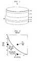
- FIG. 2illustrates a portion of an exemplary conventional Stoner-Wohlfarth astroid.
- the dotsindicate full and half select fields. For fields larger than the astroid boundary, the device switches, whereas for fields smaller than the astroid boundary, the device does not switch.
- the goalis to design an astroid wherein half select fields lie within the astroid boundary and full select fields lie outside of the astroid boundary.
- the astroid boundaryIn order to have sufficient write margins, one wants the astroid boundary to be such as to allow large half select fields that do not switch the device and, simultaneously, allow small full select fields that do switch the device.
- the astroid shape and the size of the switching fieldsdepends on the device design.
- Some conventional designsemploy a single layer shaped like an ellipse.
- the single domain theory for an elliptical single layeris referred to as Stoner-Wohlfarth theory, and the astroid shape associated therewith is the Stoner-Wohlfarth astroid, as shown in FIG. 2 .
- the present techniquesprovide a new improved shaped astroid that is better than the Stoner-Wohlfarth astroid in that it writes in very small full select fields, and yet does not switch in much larger half select fields.
- the switching fieldis often referred to as coercivity H c .
- any small magnetic layercreates its own magnetic field which exists outside the magnetic layer and in a direction opposite to the direction of its magnetization. This magnetic field is called the dipole field H d .
- an easy axis amplifiercomprises two magnetic layers coupled together with a small amount of parallel exchange coupling, the dimensions of which are shown in FIG. 3 .
- FIG. 3is a diagram illustrating an exemplary easy axis amplifier configuration and dimensions.
- the magnetic layers 108 and 110(separated by nonmagnetic layer 112 ) may be of an equal thickness, t.
- the magnetic layersmay be elliptical.
- the magnetic layersmay be of any suitable shape, e.g., circular.
- bthe width of the ellipse
- tthe thicknesses of each magnetic layer
- Jis the exchange coupling in ergs per square centimeter (erg/cm 2 )
- FIG. 4Ais a hysteresis loop for an exemplary easy axis amplifier.
- the easy axis dipole field(proportional to the net magnetic moment in the easy axis direction) is plotted as a function of applied easy axis field H e .
- H d8 ⁇ ⁇ ⁇ ⁇ t ⁇ ⁇ n x ⁇ M S b . Note, that because of J, H d >>H t .
- the direction of the magnetizations of the two layersis shown schematically at the top of FIG. 4A for negative applied magnetic fields, zero applied magnetic field and positive applied magnetic fields.
- FIG. 4Bis another hysteresis loop for an exemplary easy axis amplifier.
- H ccan be made to be close to zero. Either loop shape works for an amplifier, as long as J is close to 4 ⁇ ⁇ ⁇ ⁇ t 2 ⁇ M S 2 ⁇ n x b such that either H t or H c is small.
- the easy axis amplifiershould produce a relatively large dipole field H d and switch in a relatively small threshold field H t (or coercive field).
- the free layershould have a, relatively large coercivity H c and a low dipole field H fl . Namely, the free layer should have a coercivity larger than H d ⁇ H t ⁇ H fl such that the free layer does not switch in an easy axis field alone.
- FIG. 5is a diagram illustrating an exemplary semiconductor configuration with a free magnetic layer comprising two highly anti-parallel coupled layers.
- this exemplary semiconductor devicecomprises easy axis amplifier 106 (namely magnetic layers 110 and 108 separated by nonmagnetic layer 112 ).
- Easy axis amplifier 106is separated from free magnetic layer 502 by nonmagnetic spacer layer 104 .
- Free magnetic layer 502comprises tightly anti-parallel coupled magnetic layers 504 and 508 separated by strong anti-parallel coupling spacer layer 506 .
- each of the two magnetic layerhas a small amount of intrinsic anisotropy. If the two layers are of substantially the same thickness, then there is little net moment (i.e., resulting in a small dipole field) and a large coercivity (due to the intrinsic anisotropy).
- the free magnetic layermay be deposited on top of, or beneath, the amplifier.
- the free magnetic layeris separated from the amplifier by a nonmagnetic spacer layer which provides substantially no coupling, such that the free magnetic layer and the amplifier interact essentially only by dipole fields, as described above in conjunction with FIG. 1 .
- the free magnetic layeris pointing to the right, and it is desired to write it to the left.
- Enough fieldmust be applied to overcome the dipole field from the free magnetic layer, in addition to the threshold field.
- the free layernow experiences an applied field of H t +H fl , to the right, and a dipole field from the amplifier of H d , to the left, for a total of H d ⁇ H t ⁇ H fl to the left.
- FIGS. 6A–Care hysteresis loops for an exemplary set of applied fields. Namely, FIGS. 6A–C show the effective fields that the free magnetic layer experiences, as a function of easy axis applied magnetic field, assuming the free magnetic layer is pointing to the right.
- FIG. 6AAn illustrative dipole field experienced from the amplifier is shown in FIG. 6A . Because the free magnetic layer is pointing to the right, in a zero applied magnetic field, the amplifier points to the left. Thus in a zero applied magnetic field, the free layer experiences a positive field from the dipole field of the amplifier.
- the amplifierswitches so that the free magnetic layer experiences a negative field from the dipole field of the amplifier.
- An illustrative applied field that the free layer experiencesis shown in FIG. 6B .
- the sum of the dipole field from the amplifier and the applied field that the free magnetic layer experiencesis shown in FIG. 6C .
- FIG. 7shows an illustrative astroid expected from this exemplary configuration. Only for very large negative easy axis fields ⁇ H c ⁇ H d will the free magnetic layer switch with no hard axis field applied. The usual Stoner-Wohlfarth astroid is also shown plotted in FIG. 7 , offset by ⁇ H d . This area of the plot is shown merely for completeness, because these fields are too large to be of interest.
- a preferred methodis to use an element, or alloy, in the nonmagnetic layer, e.g., nonmagnetic layer 112 of FIG. 1 , which provides the correct amount of exchange coupling.
- alloysincluding, but not limited to alloys comprising one of the following: ruthenium, osmium, rhenium, rhodium, molybdenum, iridium, chromium, copper, vanadium and combinations comprising at least one of the foregoing.
- Another method that may be employed to weakly parallel couple the magnetic layers of the amplifieris to use a nonmagnetic layer, e.g., nonmagnetic layer 112 of FIG. 1 , which gives very large parallel coupling (for example ruthenium), and then add a dusting layer to reduce this coupling.
- a nonmagnetic layere.g., nonmagnetic layer 112 of FIG. 1
- rutheniumvery large parallel coupling
- a dusting layerfor example, one or both interfaces, or the middle of the ruthenium layer, could be dusted with a few Angstroms of another material which has substantially no coupling (or much smaller coupling), thus reducing the net coupling.
- a further method that may be employed to weakly parallel couple the magnetic layers of the amplifieris to have the two magnetic layers separated by only a thin layer of a nonmagnetic material, e.g., nonmagnetic layer 112 of FIG. 1 , with pinholes in it.
- the nonmagnetic materialserves to largely decouple the two layers, while the pinholes allow the two layers to be parallel coupled, but only weakly parallel coupled.
- a different methodis to use Neel coupling by making the interfaces rough, however, this is often not preferred because interface roughness has other deleterious effects.
- FIG. 8shows an illustrative astroid calculated using the single domain theory for an exemplary composite semiconductor device structure.
- the composite semiconductor device structurecomprised a free layer consisting of a single thin layer (1.5 nanometers (nm)) with a large amount of intrinsic anisotropy (80 Oersteds (Oe)).
- the amplifieris composed of two layers, each four nm thick, weakly coupled together by parallel exchange coupling.
- the astroidshows the expected L-shaped behavior.
- FIG. 9shows an illustrative astroid calculated using the single domain theory for another exemplary composite semiconductor device structure.
- This structurehas a free layer comprising two magnetic layers (1.5 nm and 1.6 nm thick) strongly anti-parallel coupled together, each with two Oe of intrinsic anisotropy.
- the amplifier employedhas the same configuration as that in the structure of FIG. 8 , above.
- FIG. 10shows an illustrative astroid calculated using the single domain theory for another exemplary composite semiconductor device structure.
- the same amplifier as that described in conjunction with the description of FIG. 8 , above,is employed.
- the free layeris a single layer, four nm thick, with an intrinsic anisotropy of 94 Oe.
- the astroidis shown to close up again. This is due to canting of the amplifier structure by the dipole field of the free layer, an effect that was ignored in the discussion above.
- This closing up of the astroidprovides even larger write margins by allowing even larger hard axis half select fields, without switching. In order to take advantage of this feature most effectively, the hard axis field should be removed first. This is shown in FIG. 10 .
- the easy and hard axis fieldscan be applied in any order. It does not matter if the hard axis field is set to a value larger than the closed region, as shown by the dot in FIG. 10 . Then, the hard axis field should be removed first. This ensures that the applied field moves through the open part of the astroid so that the bit is written. Finally, the easy axis field should be removed.
Landscapes
- Engineering & Computer Science (AREA)
- Computer Hardware Design (AREA)
- Mram Or Spin Memory Techniques (AREA)
- Hall/Mr Elements (AREA)
Abstract
Description
The present invention relates to semiconductor devices and, more particularly, to techniques for improving semiconductor device performance.
Semiconductor devices, i.e., magnetic random access memory (MRAM) devices use magnetic memory cells to store information. A cell is typically a submicron piece of magnetic material. The magnetic memory cell may be an ellipse, having the dimensions, e.g., of 300 nanometers (nm) by 600 nm in area and five nm thick.
Information is stored in the device as the direction of the magnetization of a free layer in the magnetic memory cell, pointing either right or left, to store either a “1” or a “0.” When the cell is sitting in a zero applied magnetic field, the magnetization of the cell is stable, pointing either right or left. The application of a magnetic field can switch the magnetization of the free layer from right to left, and vice versa, to write information to the cell.
One of the objectives of MRAM is to have a low operating power and a small area. These objectives require a low switching field for the magnetic memory cell, because a low switching field uses a low switching current, which uses less power, and because smaller currents require smaller switches, which occupy less space. Therefore, another objective of MRAM is to reduce the field required to switch the cells.
In MRAM devices there are an array of magnetic memory cells. One cell is written by sending current down a bit line and a word line. In theory, the cell at the intersection of these two lines experiences both an easy and a hard axis field, and thus switches. The easy axis is the axis along the direction the magnetization typically lies and the hard axis is perpendicular to this easy axis. Cells on the column line only feel the easy axis field (a half select field), and the cells on the row line only feel the hard axis field (half select field). These half selected cells are not meant to be switched. However, during actual operation of an MRAM device, factors, such as variations in the device, cause some of the half selected cells to be arbitrarily switched, placing the reliability and validity of the stored data in question.
Thus, it would be desirable to have a semiconductor device with a low operating power and a small area, and wherein the arbitrary switching of half selected cells is reduced or eliminated.
The present invention provides techniques for improved semiconductor device performance. In one aspect of the invention, a semiconductor device is provided. The device comprises at least one free magnetic layer, and a magnetic amplifier interacting with the free magnetic layer comprising two or more magnetic layers with at least one nonmagnetic layer therebetween. The nonmagnetic layer may be configured to provide parallel exchange coupling J of the magnetic layers in a range of
the magnetic layers having a long axis and a short axis, wherein t is a thickness of each magnetic layer, Msis magnetization, nyis a demagnetizing factor defined along the short axis of the magnetic layer and b is a diameter along the short axis of the magnetic layers.
the magnetic layers having a long axis and a short axis, wherein t is a thickness of each magnetic layer, Msis magnetization, nyis a demagnetizing factor defined along the short axis of the magnetic layer and b is a diameter along the short axis of the magnetic layers.
In another aspect of the invention, a method for switching a semiconductor device having at least one free magnetic layer comprises the following steps. An easy axis amplifier interacting with the free magnetic layer is provided comprising two or more magnetic layers with at least one nonmagnetic layer therebetween. The amplifier is written to produce a dipole field to switch the device.
A more complete understanding of the present invention, as well as further features and advantages of the present invention, will be obtained by reference to the following detailed description and drawings.
The magnetization of freemagnetic layer 102 can be changed to write information to the device. Further, as will be described in detail below,nonmagnetic spacer layer 104 prevents direct exchange coupling of freemagnetic layer 102 andeasy axis amplifier 106.
As presented in the description herein, the layers ofsemiconductor device 100 are assumed to be elliptical in shape. However, in accordance with the teachings herein, the layers ofsemiconductor device 100 may have any suitable shape or configuration, such as, but not limited to, circular, rectangular or hexagonal shape. The exact shape of the device layers is not of primary importance.
According to the techniques presented herein, a magnetic amplifier is used to amplify a small applied field into a large dipole field that writes the device. For ease of reference, the following description will be divided into the following sections; (I) Writing MRAM, (II) Definitions of Types of Fields, (III) Easy Axis Amplifier, (IV) Basic Idea of the Composite Structure and (V) Methods to Achieve Weak Parallel Coupling.
(I) Writing MRAM
Writing a semiconductor device, such assemiconductor device 100 described above in conjunction with the description ofFIG. 1 , will be presented as follows. The curve in easy axis x and hard axis y fields, which shows when the semiconductor device switches, is typically called an astroid.FIG. 2 illustrates a portion of an exemplary conventional Stoner-Wohlfarth astroid. InFIG. 2 , the dots indicate full and half select fields. For fields larger than the astroid boundary, the device switches, whereas for fields smaller than the astroid boundary, the device does not switch.
The goal is to design an astroid wherein half select fields lie within the astroid boundary and full select fields lie outside of the astroid boundary. In order to have sufficient write margins, one wants the astroid boundary to be such as to allow large half select fields that do not switch the device and, simultaneously, allow small full select fields that do switch the device.
The astroid shape and the size of the switching fields depends on the device design. Some conventional designs employ a single layer shaped like an ellipse. The single domain theory for an elliptical single layer is referred to as Stoner-Wohlfarth theory, and the astroid shape associated therewith is the Stoner-Wohlfarth astroid, as shown inFIG. 2 . The present techniques provide a new improved shaped astroid that is better than the Stoner-Wohlfarth astroid in that it writes in very small full select fields, and yet does not switch in much larger half select fields.
(II) Definitions of Types of Fields
Presented herein are definitions of the fields present during operation of a semiconductor device, e.g.,semiconductor device 100 described above in conjunction with the description ofFIG. 1 . The switching field is often referred to as coercivity Hc. In addition, any small magnetic layer creates its own magnetic field which exists outside the magnetic layer and in a direction opposite to the direction of its magnetization. This magnetic field is called the dipole field Hd.
(III) Easy Axis Amplifier
As was described above in conjunction with the description ofFIG. 1 , an easy axis amplifier comprises two magnetic layers coupled together with a small amount of parallel exchange coupling, the dimensions of which are shown inFIG. 3 .FIG. 3 is a diagram illustrating an exemplary easy axis amplifier configuration and dimensions. Themagnetic layers 108 and110 (separated by nonmagnetic layer112) may be of an equal thickness, t. As shown inFIG. 3 , the magnetic layers may be elliptical. However, as was mentioned above, the magnetic layers may be of any suitable shape, e.g., circular.
The amplifier structure, as shown inFIG. 3 , can be made to produce a large dipole field Hd, yet switch in a small threshold field Ht(as compared to its dipole field). According to single domain theory, Htis given by the expression
which only holds for therange
wherein Msis magnetization, b is the width of the ellipse, t is the thicknesses of each magnetic layer, J is the exchange coupling in ergs per square centimeter (erg/cm2) and nxand nyare the reduced demagnetizing factors defined along the x-axis, the long axis, and the y-axis, the short axis, respectively (nx=0.32 and ny=0.9 for an aspect ratio of two). Note, that by adjusting J to be close to
Htcan be made to be close to zero.
which only holds for the
wherein Msis magnetization, b is the width of the ellipse, t is the thicknesses of each magnetic layer, J is the exchange coupling in ergs per square centimeter (erg/cm2) and nxand nyare the reduced demagnetizing factors defined along the x-axis, the long axis, and the y-axis, the short axis, respectively (nx=0.32 and ny=0.9 for an aspect ratio of two). Note, that by adjusting J to be close to
Htcan be made to be close to zero.
The corresponding hysteresis loop of this amplifier structure is shown inFIG. 4A .FIG. 4A is a hysteresis loop for an exemplary easy axis amplifier. InFIG. 4A , the easy axis dipole field (proportional to the net magnetic moment in the easy axis direction) is plotted as a function of applied easy axis field He.
In a zero applied magnetic field, there is no moment, namely because the two magnetic layers are anti-parallel. In small applied magnetic fields, the magnetic layers scissor out until they are parallel, i.e., when He=Ht. At this point, the magnetic layers produce a large dipole field Hd. Hdis given by the expression
Note, that because of J, Hd>>Ht. The direction of the magnetizations of the two layers is shown schematically at the top ofFIG. 4A for negative applied magnetic fields, zero applied magnetic field and positive applied magnetic fields.
Note, that because of J, Hd>>Ht. The direction of the magnetizations of the two layers is shown schematically at the top of
When
the loop is an open loop, with coercivity
as shown inFIG. 4B .FIG. 4B is another hysteresis loop for an exemplary easy axis amplifier. Again, by adjusting J to be close to
Hccan be made to be close to zero. Either loop shape works for an amplifier, as long as J is close to
such that either Htor Hcis small.
(IV) Basic Idea of the Composite Structure
the loop is an open loop, with coercivity
as shown in
Hccan be made to be close to zero. Either loop shape works for an amplifier, as long as J is close to
such that either Htor Hcis small.
(IV) Basic Idea of the Composite Structure
There are two ingredients to the exemplary composite semiconductor device structure, e.g., the structure described in conjunction with the description ofFIG. 1 , an easy axis amplifier and a free layer. The easy axis amplifier should produce a relatively large dipole field Hdand switch in a relatively small threshold field Ht(or coercive field). The free layer should have a, relatively large coercivity Hcand a low dipole field Hfl. Namely, the free layer should have a coercivity larger than Hd−Ht−Hflsuch that the free layer does not switch in an easy axis field alone.
The free layer should also have a small dipole field Hflso that the free layer does not disturb the amplifier too much. The free layer may comprise an ellipse with a large amount of intrinsic anisotropy. It could also comprise an ellipse composed of two magnetic layers tightly anti-parallel coupled, as shown inFIG. 5 .FIG. 5 is a diagram illustrating an exemplary semiconductor configuration with a free magnetic layer comprising two highly anti-parallel coupled layers. As shown inFIG. 5 , this exemplary semiconductor device comprises easy axis amplifier106 (namelymagnetic layers Easy axis amplifier 106 is separated from freemagnetic layer 502 bynonmagnetic spacer layer 104. Freemagnetic layer 502 comprises tightly anti-parallel coupledmagnetic layers coupling spacer layer 506.
If the free magnetic layer comprises two tightly anti-parallel coupled layers, each of the two magnetic layer has a small amount of intrinsic anisotropy. If the two layers are of substantially the same thickness, then there is little net moment (i.e., resulting in a small dipole field) and a large coercivity (due to the intrinsic anisotropy).
The free magnetic layer may be deposited on top of, or beneath, the amplifier. The free magnetic layer is separated from the amplifier by a nonmagnetic spacer layer which provides substantially no coupling, such that the free magnetic layer and the amplifier interact essentially only by dipole fields, as described above in conjunction withFIG. 1 .
Suppose, by way of example, that the free magnetic layer is pointing to the right, and it is desired to write it to the left. A field may be applied to the right to write the amplifier at roughly H=Ht+Hfl. Enough field must be applied to overcome the dipole field from the free magnetic layer, in addition to the threshold field. The free layer now experiences an applied field of Ht+Hfl, to the right, and a dipole field from the amplifier of Hd, to the left, for a total of Hd−Ht−Hflto the left.
Since Hc>Hd−Ht−Hfl, this applied field will not write the free layer to the left. Increasing the applied field will not write it either, as this increased applied field only decreases the net field that the free magnetic layer experiences. Applying a very large negative field −Hc−Hdwould write the free magnetic layer, and should be avoided. If a small hard axis field were applied when H=Hd−Ht−Hfl, then the free layer does write via the Stoner-Wohlfarth process. Therefore, according to the techniques presented herein, the free magnetic layer will only write if both a small hard axis field and a small easy axis field are applied.
This set of fields is depicted inFIGS. 6A–C .FIGS. 6A–C are hysteresis loops for an exemplary set of applied fields. Namely,FIGS. 6A–C show the effective fields that the free magnetic layer experiences, as a function of easy axis applied magnetic field, assuming the free magnetic layer is pointing to the right.
An illustrative dipole field experienced from the amplifier is shown inFIG. 6A . Because the free magnetic layer is pointing to the right, in a zero applied magnetic field, the amplifier points to the left. Thus in a zero applied magnetic field, the free layer experiences a positive field from the dipole field of the amplifier.
At the small positive field Ht+Hfl, the amplifier switches so that the free magnetic layer experiences a negative field from the dipole field of the amplifier. An illustrative applied field that the free layer experiences is shown inFIG. 6B . The sum of the dipole field from the amplifier and the applied field that the free magnetic layer experiences is shown inFIG. 6C .
At the very small easy axis field Ht+Hflit is also possible to switch the free magnetic layer if a small hard axis field is also applied. Again, the usual Stoner-Wohlfarth astroid is plotted inFIG. 7 , offset by Hd. The astroid is drawn as a dotted boundary. The actual switching astroid is given by the solid L-shaped curve which gives the minimum fields for which the free layer switches. This L-shaped astroid represents an ideal astroid for MRAM. Namely, the free layer switches in very small fields (Ht+Hfl), and the write margins are large because the half select fields can be much larger than the full select field.
(V) Methods to Achieve Weak Parallel Coupling
There are many ways to get the two magnetic layers of the amplifier, e.g., the amplifier described above in conjunction with the descriptions ofFIG. 1 andFIG. 3 , to be weakly parallel coupled. A preferred method is to use an element, or alloy, in the nonmagnetic layer, e.g.,nonmagnetic layer 112 ofFIG. 1 , which provides the correct amount of exchange coupling. There are many such alloys, including, but not limited to alloys comprising one of the following: ruthenium, osmium, rhenium, rhodium, molybdenum, iridium, chromium, copper, vanadium and combinations comprising at least one of the foregoing.
Another method that may be employed to weakly parallel couple the magnetic layers of the amplifier is to use a nonmagnetic layer, e.g.,nonmagnetic layer 112 ofFIG. 1 , which gives very large parallel coupling (for example ruthenium), and then add a dusting layer to reduce this coupling. For example, one or both interfaces, or the middle of the ruthenium layer, could be dusted with a few Angstroms of another material which has substantially no coupling (or much smaller coupling), thus reducing the net coupling.
A further method that may be employed to weakly parallel couple the magnetic layers of the amplifier is to have the two magnetic layers separated by only a thin layer of a nonmagnetic material, e.g.,nonmagnetic layer 112 ofFIG. 1 , with pinholes in it. The nonmagnetic material serves to largely decouple the two layers, while the pinholes allow the two layers to be parallel coupled, but only weakly parallel coupled. A different method is to use Neel coupling by making the interfaces rough, however, this is often not preferred because interface roughness has other deleterious effects.
Although illustrative embodiments of the present invention have been described herein, it is to be understood that the invention is not limited to those precise embodiments, and that various other changes and modifications may be made by one skilled in the art without departing from the scope or spirit of the invention.
Claims (19)
1. A semiconductor device comprising:
at least one free magnetic layer; and
a magnetic amplifier interacting with the free magnetic layer and comprising two or more magnetic layers with at least one nonmagnetic layer therebetween.
2. The device ofclaim 1 , wherein the nonmagnetic layer is configured to provide parallel exchange coupling J of the magnetic layers in a range of
the magnetic layers having a long axis and a short axis, wherein t is a thickness of each magnetic layer, Msis magnetization, nyis a demagnetizing factor defined along the short axis of the magnetic layers and b is a diameter along the short axis of the magnetic layers.
3. The device ofclaim 1 , wherein the nonmagnetic layer is configured to provide parallel exchange coupling J of the magnetic layers such that a switching threshold field Htassociated with the magnetic amplifier is substantially zero.
4. The device ofclaim 1 , wherein the nonmagnetic layer is configured to provide parallel exchange coupling J of the magnetic layers such that a coercivity Hcassociated with the magnetic amplifier is substantially zero.
5. The device ofclaim 1 , wherein the nonmagnetic layer is configured to provide parallel exchange coupling J of the magnetic layers such that a threshold field Htand a coercivity Hcassociated with the magnetic amplifier are substantially zero.
6. The device ofclaim 1 , further comprising a nonmagnetic spacer layer between the free magnetic layer and the magnetic amplifier.
7. The device ofclaim 6 , wherein the nonmagnetic spacer layer prevents coupling of the free magnetic layer and the magnetic amplifier.
8. The device ofclaim 1 , wherein the free magnetic layer and the magnetic amplifier interact by dipole fields.
9. The device ofclaim 1 , comprising two or more free magnetic layers tightly anti-parallel coupled together.
10. The device ofclaim 1 , wherein the nonmagnetic layer comprises an alloy.
11. The device ofclaim 10 , wherein the alloy comprises an element selected from the group consisting of ruthenium, osmium, rhenium, rhodium, molybdenum, iridium, chromium, copper, vanadium and combinations comprising at least one of the foregoing.
12. The device ofclaim 1 , wherein the free layer has an elliptical shape.
13. The device ofclaim 1 , wherein the layers of the amplifier have an elliptical shape.
14. The device ofclaim 1 , wherein the amplifier comprises an easy axis amplifier.
15. The device ofclaim 1 , wherein the amplifier is deposited on top of the free layer.
16. The device ofclaim 1 , wherein the amplifier is deposited beneath the free layer.
17. A method for switching a semiconductor device having at least one free magnetic layer, the method comprising the steps of:
providing an easy axis amplifier interacting with the free magnetic layer and comprising two or more magnetic layers with at least one nonmagnetic layer therebetween; and
writing the amplifier to produce a dipole field to switch the device.
18. An integrated circuit device including at least one semiconductor device, the at least one semiconductor device comprising:
at least one free magnetic layer; and
a magnetic amplifier interacting with the free magnetic layer and comprising two or more magnetic layers with at least one nonmagnetic layer therebetween.
19. The integrated circuit device ofclaim 18 , wherein the integrated circuit device comprises a magnetic random access memory.
Priority Applications (1)
| Application Number | Priority Date | Filing Date | Title |
|---|---|---|---|
| US10/725,985US6987691B2 (en) | 2003-12-02 | 2003-12-02 | Easy axis magnetic amplifier |
Applications Claiming Priority (1)
| Application Number | Priority Date | Filing Date | Title |
|---|---|---|---|
| US10/725,985US6987691B2 (en) | 2003-12-02 | 2003-12-02 | Easy axis magnetic amplifier |
Publications (2)
| Publication Number | Publication Date |
|---|---|
| US20050117389A1 US20050117389A1 (en) | 2005-06-02 |
| US6987691B2true US6987691B2 (en) | 2006-01-17 |
Family
ID=34620404
Family Applications (1)
| Application Number | Title | Priority Date | Filing Date |
|---|---|---|---|
| US10/725,985Expired - Fee RelatedUS6987691B2 (en) | 2003-12-02 | 2003-12-02 | Easy axis magnetic amplifier |
Country Status (1)
| Country | Link |
|---|---|
| US (1) | US6987691B2 (en) |
Families Citing this family (58)
| Publication number | Priority date | Publication date | Assignee | Title |
|---|---|---|---|---|
| US8730031B2 (en) | 2005-04-28 | 2014-05-20 | Proteus Digital Health, Inc. | Communication system using an implantable device |
| US8912908B2 (en) | 2005-04-28 | 2014-12-16 | Proteus Digital Health, Inc. | Communication system with remote activation |
| US8836513B2 (en) | 2006-04-28 | 2014-09-16 | Proteus Digital Health, Inc. | Communication system incorporated in an ingestible product |
| US9198608B2 (en) | 2005-04-28 | 2015-12-01 | Proteus Digital Health, Inc. | Communication system incorporated in a container |
| EP3827747A1 (en) | 2005-04-28 | 2021-06-02 | Otsuka Pharmaceutical Co., Ltd. | Pharma-informatics system |
| US8802183B2 (en) | 2005-04-28 | 2014-08-12 | Proteus Digital Health, Inc. | Communication system with enhanced partial power source and method of manufacturing same |
| US8547248B2 (en) | 2005-09-01 | 2013-10-01 | Proteus Digital Health, Inc. | Implantable zero-wire communications system |
| CN101278353B (en)* | 2005-09-30 | 2013-10-02 | Nxp股份有限公司 | Nanowire magnetic random access memory |
| JP2009544338A (en) | 2006-05-02 | 2009-12-17 | プロテウス バイオメディカル インコーポレイテッド | Treatment regimen customized to the patient |
| EP2087589B1 (en)* | 2006-10-17 | 2011-11-23 | Proteus Biomedical, Inc. | Low voltage oscillator for medical devices |
| SG175681A1 (en) | 2006-10-25 | 2011-11-28 | Proteus Biomedical Inc | Controlled activation ingestible identifier |
| US8718193B2 (en) | 2006-11-20 | 2014-05-06 | Proteus Digital Health, Inc. | Active signal processing personal health signal receivers |
| CN101686800A (en) | 2007-02-01 | 2010-03-31 | 普罗秋斯生物医学公司 | Ingestible Event Marker System |
| US8956288B2 (en) | 2007-02-14 | 2015-02-17 | Proteus Digital Health, Inc. | In-body power source having high surface area electrode |
| EP2124725A1 (en) | 2007-03-09 | 2009-12-02 | Proteus Biomedical, Inc. | In-body device having a multi-directional transmitter |
| EP2063771A1 (en) | 2007-03-09 | 2009-06-03 | Proteus Biomedical, Inc. | In-body device having a deployable antenna |
| US8115618B2 (en) | 2007-05-24 | 2012-02-14 | Proteus Biomedical, Inc. | RFID antenna for in-body device |
| DK2192946T3 (en)* | 2007-09-25 | 2022-11-21 | Otsuka Pharma Co Ltd | In-body device with virtual dipole signal amplification |
| KR101586193B1 (en) | 2007-11-27 | 2016-01-18 | 프로테우스 디지털 헬스, 인코포레이티드 | Transbody communication systems employing communication channels |
| CN104376659B (en)* | 2008-03-05 | 2019-10-25 | 普罗透斯数字保健公司 | The ingestible event flag of multi-modal communications and system, and the method using it |
| AU2009268827B2 (en) | 2008-07-08 | 2013-10-24 | Proteus Digital Health, Inc. | Ingestible event marker data framework |
| MY154217A (en) | 2008-08-13 | 2015-05-15 | Proteus Digital Health Inc | Ingestible circuitry |
| US8036748B2 (en)* | 2008-11-13 | 2011-10-11 | Proteus Biomedical, Inc. | Ingestible therapy activator system and method |
| EP2358270A4 (en)* | 2008-12-11 | 2014-08-13 | Proteus Digital Health Inc | Evaluation of gastrointestinal function using portable electroviscerography systems and methods of using the same |
| US9439566B2 (en) | 2008-12-15 | 2016-09-13 | Proteus Digital Health, Inc. | Re-wearable wireless device |
| US9659423B2 (en) | 2008-12-15 | 2017-05-23 | Proteus Digital Health, Inc. | Personal authentication apparatus system and method |
| TWI503101B (en) | 2008-12-15 | 2015-10-11 | Proteus Digital Health Inc | Body-associated receiver and method |
| SG172847A1 (en) | 2009-01-06 | 2011-08-29 | Proteus Biomedical Inc | Pharmaceutical dosages delivery system |
| KR20110103446A (en) | 2009-01-06 | 2011-09-20 | 프로테우스 바이오메디컬, 인코포레이티드 | Intake-Related Biofeedback and Individualized Medical Treatment Methods and Systems |
| WO2010111403A2 (en) | 2009-03-25 | 2010-09-30 | Proteus Biomedical, Inc. | Probablistic pharmacokinetic and pharmacodynamic modeling |
| EP3906845A1 (en) | 2009-04-28 | 2021-11-10 | Otsuka Pharmaceutical Co., Ltd. | Highly reliable ingestible event markers |
| EP2432458A4 (en) | 2009-05-12 | 2014-02-12 | Proteus Digital Health Inc | Ingestible event markers comprising an ingestible component |
| US8558563B2 (en) | 2009-08-21 | 2013-10-15 | Proteus Digital Health, Inc. | Apparatus and method for measuring biochemical parameters |
| TWI517050B (en) | 2009-11-04 | 2016-01-11 | 普羅托斯數位健康公司 | System for supply chain management |
| UA109424C2 (en) | 2009-12-02 | 2015-08-25 | PHARMACEUTICAL PRODUCT, PHARMACEUTICAL TABLE WITH ELECTRONIC MARKER AND METHOD OF MANUFACTURING PHARMACEUTICAL TABLETS | |
| BR112012019212A2 (en) | 2010-02-01 | 2017-06-13 | Proteus Digital Health Inc | data collection system |
| WO2011127252A2 (en) | 2010-04-07 | 2011-10-13 | Proteus Biomedical, Inc. | Miniature ingestible device |
| TWI557672B (en) | 2010-05-19 | 2016-11-11 | 波提亞斯數位康健公司 | Computer system and computer-implemented method to track medication from manufacturer to a patient, apparatus and method for confirming delivery of medication to a patient, patient interface device |
| JP2014504902A (en) | 2010-11-22 | 2014-02-27 | プロテウス デジタル ヘルス, インコーポレイテッド | Ingestible device with medicinal product |
| WO2012125425A2 (en) | 2011-03-11 | 2012-09-20 | Proteus Biomedical, Inc. | Wearable personal body associated device with various physical configurations |
| US9756874B2 (en) | 2011-07-11 | 2017-09-12 | Proteus Digital Health, Inc. | Masticable ingestible product and communication system therefor |
| WO2015112603A1 (en) | 2014-01-21 | 2015-07-30 | Proteus Digital Health, Inc. | Masticable ingestible product and communication system therefor |
| PH12014500174A1 (en) | 2011-07-21 | 2024-02-12 | Proteus Digital Health Inc | Mobile communication device, system, and method |
| US9235683B2 (en) | 2011-11-09 | 2016-01-12 | Proteus Digital Health, Inc. | Apparatus, system, and method for managing adherence to a regimen |
| EP2874886B1 (en) | 2012-07-23 | 2023-12-20 | Otsuka Pharmaceutical Co., Ltd. | Techniques for manufacturing ingestible event markers comprising an ingestible component |
| AU2013331417B2 (en) | 2012-10-18 | 2016-06-02 | Proteus Digital Health, Inc. | Apparatus, system, and method to adaptively optimize power dissipation and broadcast power in a power source for a communication device |
| US11149123B2 (en) | 2013-01-29 | 2021-10-19 | Otsuka Pharmaceutical Co., Ltd. | Highly-swellable polymeric films and compositions comprising the same |
| WO2014144738A1 (en) | 2013-03-15 | 2014-09-18 | Proteus Digital Health, Inc. | Metal detector apparatus, system, and method |
| JP6498177B2 (en) | 2013-03-15 | 2019-04-10 | プロテウス デジタル ヘルス, インコーポレイテッド | Identity authentication system and method |
| EP3005281A4 (en) | 2013-06-04 | 2017-06-28 | Proteus Digital Health, Inc. | System, apparatus and methods for data collection and assessing outcomes |
| US9796576B2 (en) | 2013-08-30 | 2017-10-24 | Proteus Digital Health, Inc. | Container with electronically controlled interlock |
| CA2965941C (en) | 2013-09-20 | 2020-01-28 | Proteus Digital Health, Inc. | Methods, devices and systems for receiving and decoding a signal in the presence of noise using slices and warping |
| WO2015044722A1 (en) | 2013-09-24 | 2015-04-02 | Proteus Digital Health, Inc. | Method and apparatus for use with received electromagnetic signal at a frequency not known exactly in advance |
| US10084880B2 (en) | 2013-11-04 | 2018-09-25 | Proteus Digital Health, Inc. | Social media networking based on physiologic information |
| US11051543B2 (en) | 2015-07-21 | 2021-07-06 | Otsuka Pharmaceutical Co. Ltd. | Alginate on adhesive bilayer laminate film |
| KR20210018961A (en) | 2016-07-22 | 2021-02-18 | 프로테우스 디지털 헬스, 인코포레이티드 | Electromagnetic sensing and detection of ingestible event markers |
| CN109963499B (en) | 2016-10-26 | 2022-02-25 | 大冢制药株式会社 | Method for manufacturing capsules with ingestible event markers |
| IT201900021606A1 (en) | 2019-11-19 | 2021-05-19 | St Microelectronics Srl | PHASE CHANGE MEMORY DEVICE AND METHOD OF PROGRAMMING A PHASE CHANGE MEMORY DEVICE |
Citations (4)
| Publication number | Priority date | Publication date | Assignee | Title |
|---|---|---|---|---|
| US5841692A (en)* | 1996-03-18 | 1998-11-24 | International Business Machines Corporation | Magnetic tunnel junction device with antiferromagnetically coupled pinned layer |
| US6381171B1 (en)* | 1999-05-19 | 2002-04-30 | Kabushiki Kaisha Toshiba | Magnetic element, magnetic read head, magnetic storage device, magnetic memory device |
| US6531723B1 (en)* | 2001-10-16 | 2003-03-11 | Motorola, Inc. | Magnetoresistance random access memory for improved scalability |
| US6831857B2 (en)* | 2001-12-28 | 2004-12-14 | Kabushiki Kaisha Toshiba | Magnetic memory |
- 2003
- 2003-12-02USUS10/725,985patent/US6987691B2/ennot_activeExpired - Fee Related
Patent Citations (4)
| Publication number | Priority date | Publication date | Assignee | Title |
|---|---|---|---|---|
| US5841692A (en)* | 1996-03-18 | 1998-11-24 | International Business Machines Corporation | Magnetic tunnel junction device with antiferromagnetically coupled pinned layer |
| US6381171B1 (en)* | 1999-05-19 | 2002-04-30 | Kabushiki Kaisha Toshiba | Magnetic element, magnetic read head, magnetic storage device, magnetic memory device |
| US6531723B1 (en)* | 2001-10-16 | 2003-03-11 | Motorola, Inc. | Magnetoresistance random access memory for improved scalability |
| US6831857B2 (en)* | 2001-12-28 | 2004-12-14 | Kabushiki Kaisha Toshiba | Magnetic memory |
Also Published As
| Publication number | Publication date |
|---|---|
| US20050117389A1 (en) | 2005-06-02 |
Similar Documents
| Publication | Publication Date | Title |
|---|---|---|
| US6987691B2 (en) | Easy axis magnetic amplifier | |
| US7274057B2 (en) | Techniques for spin-flop switching with offset field | |
| US6545906B1 (en) | Method of writing to scalable magnetoresistance random access memory element | |
| US6633498B1 (en) | Magnetoresistive random access memory with reduced switching field | |
| US6531723B1 (en) | Magnetoresistance random access memory for improved scalability | |
| US8218357B2 (en) | Spin torque transfer cell structure utilizing field-induced antiferromagnetic or ferromagnetic coupling | |
| US7502253B2 (en) | Spin-transfer based MRAM with reduced critical current density | |
| US7230845B1 (en) | Magnetic devices having a hard bias field and magnetic memory devices using the magnetic devices | |
| US6649960B1 (en) | Synthetic free layer structure for MRAM devices | |
| US8742518B2 (en) | Magnetic tunnel junction with free layer having exchange coupled magnetic elements | |
| US6765819B1 (en) | Magnetic memory device having improved switching characteristics | |
| JP4594839B2 (en) | Magnetic random access memory, method for manufacturing magnetic random access memory, and data writing method for magnetic random access memory | |
| US8852761B2 (en) | CoFeSiB/Pt multilayers exhibiting perpendicular magnetic anisotropy | |
| US7838953B2 (en) | Magnetic memory cell and magnetic random access memory | |
| JP3964818B2 (en) | Magnetic random access memory | |
| US7599156B2 (en) | Magnetoresistive element having specially shaped ferromagnetic layer | |
| JP2002289807A (en) | Magnetic memory device and magnetoresistive element | |
| US7525837B2 (en) | Magnetoresistive effect element and magnetic memory | |
| TWI885306B (en) | Magnetic memory device | |
| US20050047262A1 (en) | Magnetic film, multilayer magnetic film, method and mechanism of magnetization inversion of magnetic film, and magnetic random access memory | |
| US8034637B2 (en) | Techniques for coupling in semiconductor devices | |
| JP4594694B2 (en) | Magnetoresistive effect element | |
| US7002194B2 (en) | Via AP switching | |
| US20030235074A1 (en) | Magnetic memory device | |
| JP2005129801A (en) | Magnetic storage element and magnetic memory |
Legal Events
| Date | Code | Title | Description |
|---|---|---|---|
| AS | Assignment | Owner name:INTERNATIONAL BUSINESS MACHINES CORPORATION, NEW Y Free format text:ASSIGNMENT OF ASSIGNORS INTEREST;ASSIGNOR:WORLEDGE, DANIEL CHRISTOPHER;REEL/FRAME:014348/0026 Effective date:20031202 | |
| FEPP | Fee payment procedure | Free format text:PAYOR NUMBER ASSIGNED (ORIGINAL EVENT CODE: ASPN); ENTITY STATUS OF PATENT OWNER: LARGE ENTITY | |
| FPAY | Fee payment | Year of fee payment:4 | |
| REMI | Maintenance fee reminder mailed | ||
| FPAY | Fee payment | Year of fee payment:8 | |
| SULP | Surcharge for late payment | Year of fee payment:7 | |
| FEPP | Fee payment procedure | Free format text:MAINTENANCE FEE REMINDER MAILED (ORIGINAL EVENT CODE: REM.) | |
| LAPS | Lapse for failure to pay maintenance fees | Free format text:PATENT EXPIRED FOR FAILURE TO PAY MAINTENANCE FEES (ORIGINAL EVENT CODE: EXP.) | |
| STCH | Information on status: patent discontinuation | Free format text:PATENT EXPIRED DUE TO NONPAYMENT OF MAINTENANCE FEES UNDER 37 CFR 1.362 | |
| FP | Lapsed due to failure to pay maintenance fee | Effective date:20180117 |