US6987041B2 - Semiconductor device having both memory and logic circuit and its manufacture - Google Patents
Semiconductor device having both memory and logic circuit and its manufactureDownload PDFInfo
- Publication number
- US6987041B2 US6987041B2US09/961,264US96126401AUS6987041B2US 6987041 B2US6987041 B2US 6987041B2US 96126401 AUS96126401 AUS 96126401AUS 6987041 B2US6987041 B2US 6987041B2
- Authority
- US
- United States
- Prior art keywords
- logic circuit
- area
- film
- memory cell
- circuit area
- Prior art date
- Legal status (The legal status is an assumption and is not a legal conclusion. Google has not performed a legal analysis and makes no representation as to the accuracy of the status listed.)
- Expired - Lifetime, expires
Links
Images


Classifications
- H—ELECTRICITY
- H10—SEMICONDUCTOR DEVICES; ELECTRIC SOLID-STATE DEVICES NOT OTHERWISE PROVIDED FOR
- H10B—ELECTRONIC MEMORY DEVICES
- H10B12/00—Dynamic random access memory [DRAM] devices
- H—ELECTRICITY
- H10—SEMICONDUCTOR DEVICES; ELECTRIC SOLID-STATE DEVICES NOT OTHERWISE PROVIDED FOR
- H10D—INORGANIC ELECTRIC SEMICONDUCTOR DEVICES
- H10D84/00—Integrated devices formed in or on semiconductor substrates that comprise only semiconducting layers, e.g. on Si wafers or on GaAs-on-Si wafers
- H10D84/01—Manufacture or treatment
- H10D84/0123—Integrating together multiple components covered by H10D12/00 or H10D30/00, e.g. integrating multiple IGBTs
- H10D84/0126—Integrating together multiple components covered by H10D12/00 or H10D30/00, e.g. integrating multiple IGBTs the components including insulated gates, e.g. IGFETs
- H10D84/0135—Manufacturing their gate conductors
- H10D84/014—Manufacturing their gate conductors the gate conductors having different materials or different implants
- H—ELECTRICITY
- H01—ELECTRIC ELEMENTS
- H01L—SEMICONDUCTOR DEVICES NOT COVERED BY CLASS H10
- H01L21/00—Processes or apparatus adapted for the manufacture or treatment of semiconductor or solid state devices or of parts thereof
- H01L21/02—Manufacture or treatment of semiconductor devices or of parts thereof
- H01L21/04—Manufacture or treatment of semiconductor devices or of parts thereof the devices having potential barriers, e.g. a PN junction, depletion layer or carrier concentration layer
- H01L21/18—Manufacture or treatment of semiconductor devices or of parts thereof the devices having potential barriers, e.g. a PN junction, depletion layer or carrier concentration layer the devices having semiconductor bodies comprising elements of Group IV of the Periodic Table or AIIIBV compounds with or without impurities, e.g. doping materials
- H01L21/26—Bombardment with radiation
- H01L21/263—Bombardment with radiation with high-energy radiation
- H01L21/265—Bombardment with radiation with high-energy radiation producing ion implantation
- H01L21/26506—Bombardment with radiation with high-energy radiation producing ion implantation in group IV semiconductors
- H01L21/26513—Bombardment with radiation with high-energy radiation producing ion implantation in group IV semiconductors of electrically active species
- H—ELECTRICITY
- H01—ELECTRIC ELEMENTS
- H01L—SEMICONDUCTOR DEVICES NOT COVERED BY CLASS H10
- H01L21/00—Processes or apparatus adapted for the manufacture or treatment of semiconductor or solid state devices or of parts thereof
- H01L21/02—Manufacture or treatment of semiconductor devices or of parts thereof
- H01L21/04—Manufacture or treatment of semiconductor devices or of parts thereof the devices having potential barriers, e.g. a PN junction, depletion layer or carrier concentration layer
- H01L21/18—Manufacture or treatment of semiconductor devices or of parts thereof the devices having potential barriers, e.g. a PN junction, depletion layer or carrier concentration layer the devices having semiconductor bodies comprising elements of Group IV of the Periodic Table or AIIIBV compounds with or without impurities, e.g. doping materials
- H01L21/28—Manufacture of electrodes on semiconductor bodies using processes or apparatus not provided for in groups H01L21/20 - H01L21/268
- H01L21/28008—Making conductor-insulator-semiconductor electrodes
- H01L21/28017—Making conductor-insulator-semiconductor electrodes the insulator being formed after the semiconductor body, the semiconductor being silicon
- H01L21/28026—Making conductor-insulator-semiconductor electrodes the insulator being formed after the semiconductor body, the semiconductor being silicon characterised by the conductor
- H01L21/28035—Making conductor-insulator-semiconductor electrodes the insulator being formed after the semiconductor body, the semiconductor being silicon characterised by the conductor the final conductor layer next to the insulator being silicon, e.g. polysilicon, with or without impurities
- H—ELECTRICITY
- H10—SEMICONDUCTOR DEVICES; ELECTRIC SOLID-STATE DEVICES NOT OTHERWISE PROVIDED FOR
- H10B—ELECTRONIC MEMORY DEVICES
- H10B12/00—Dynamic random access memory [DRAM] devices
- H10B12/01—Manufacture or treatment
- H10B12/09—Manufacture or treatment with simultaneous manufacture of the peripheral circuit region and memory cells
- H—ELECTRICITY
- H10—SEMICONDUCTOR DEVICES; ELECTRIC SOLID-STATE DEVICES NOT OTHERWISE PROVIDED FOR
- H10D—INORGANIC ELECTRIC SEMICONDUCTOR DEVICES
- H10D84/00—Integrated devices formed in or on semiconductor substrates that comprise only semiconducting layers, e.g. on Si wafers or on GaAs-on-Si wafers
- H10D84/01—Manufacture or treatment
- H10D84/02—Manufacture or treatment characterised by using material-based technologies
- H10D84/03—Manufacture or treatment characterised by using material-based technologies using Group IV technology, e.g. silicon technology or silicon-carbide [SiC] technology
- H10D84/038—Manufacture or treatment characterised by using material-based technologies using Group IV technology, e.g. silicon technology or silicon-carbide [SiC] technology using silicon technology, e.g. SiGe
- H—ELECTRICITY
- H01—ELECTRIC ELEMENTS
- H01L—SEMICONDUCTOR DEVICES NOT COVERED BY CLASS H10
- H01L21/00—Processes or apparatus adapted for the manufacture or treatment of semiconductor or solid state devices or of parts thereof
- H01L21/02—Manufacture or treatment of semiconductor devices or of parts thereof
- H01L21/02104—Forming layers
- H01L21/02107—Forming insulating materials on a substrate
- H01L21/02109—Forming insulating materials on a substrate characterised by the type of layer, e.g. type of material, porous/non-porous, pre-cursors, mixtures or laminates
- H01L21/02112—Forming insulating materials on a substrate characterised by the type of layer, e.g. type of material, porous/non-porous, pre-cursors, mixtures or laminates characterised by the material of the layer
- H01L21/02123—Forming insulating materials on a substrate characterised by the type of layer, e.g. type of material, porous/non-porous, pre-cursors, mixtures or laminates characterised by the material of the layer the material containing silicon
- H01L21/02126—Forming insulating materials on a substrate characterised by the type of layer, e.g. type of material, porous/non-porous, pre-cursors, mixtures or laminates characterised by the material of the layer the material containing silicon the material containing Si, O, and at least one of H, N, C, F, or other non-metal elements, e.g. SiOC, SiOC:H or SiONC
- H01L21/02129—Forming insulating materials on a substrate characterised by the type of layer, e.g. type of material, porous/non-porous, pre-cursors, mixtures or laminates characterised by the material of the layer the material containing silicon the material containing Si, O, and at least one of H, N, C, F, or other non-metal elements, e.g. SiOC, SiOC:H or SiONC the material being boron or phosphorus doped silicon oxides, e.g. BPSG, BSG or PSG
- H—ELECTRICITY
- H01—ELECTRIC ELEMENTS
- H01L—SEMICONDUCTOR DEVICES NOT COVERED BY CLASS H10
- H01L21/00—Processes or apparatus adapted for the manufacture or treatment of semiconductor or solid state devices or of parts thereof
- H01L21/02—Manufacture or treatment of semiconductor devices or of parts thereof
- H01L21/02104—Forming layers
- H01L21/02107—Forming insulating materials on a substrate
- H01L21/02109—Forming insulating materials on a substrate characterised by the type of layer, e.g. type of material, porous/non-porous, pre-cursors, mixtures or laminates
- H01L21/02112—Forming insulating materials on a substrate characterised by the type of layer, e.g. type of material, porous/non-porous, pre-cursors, mixtures or laminates characterised by the material of the layer
- H01L21/02123—Forming insulating materials on a substrate characterised by the type of layer, e.g. type of material, porous/non-porous, pre-cursors, mixtures or laminates characterised by the material of the layer the material containing silicon
- H01L21/0217—Forming insulating materials on a substrate characterised by the type of layer, e.g. type of material, porous/non-porous, pre-cursors, mixtures or laminates characterised by the material of the layer the material containing silicon the material being a silicon nitride not containing oxygen, e.g. SixNy or SixByNz
- H—ELECTRICITY
- H10—SEMICONDUCTOR DEVICES; ELECTRIC SOLID-STATE DEVICES NOT OTHERWISE PROVIDED FOR
- H10B—ELECTRONIC MEMORY DEVICES
- H10B12/00—Dynamic random access memory [DRAM] devices
- H10B12/01—Manufacture or treatment
- H10B12/02—Manufacture or treatment for one transistor one-capacitor [1T-1C] memory cells
- H10B12/05—Making the transistor
- H—ELECTRICITY
- H10—SEMICONDUCTOR DEVICES; ELECTRIC SOLID-STATE DEVICES NOT OTHERWISE PROVIDED FOR
- H10D—INORGANIC ELECTRIC SEMICONDUCTOR DEVICES
- H10D30/00—Field-effect transistors [FET]
- H10D30/01—Manufacture or treatment
- H10D30/021—Manufacture or treatment of FETs having insulated gates [IGFET]
- H10D30/0212—Manufacture or treatment of FETs having insulated gates [IGFET] using self-aligned silicidation
- Y—GENERAL TAGGING OF NEW TECHNOLOGICAL DEVELOPMENTS; GENERAL TAGGING OF CROSS-SECTIONAL TECHNOLOGIES SPANNING OVER SEVERAL SECTIONS OF THE IPC; TECHNICAL SUBJECTS COVERED BY FORMER USPC CROSS-REFERENCE ART COLLECTIONS [XRACs] AND DIGESTS
- Y10—TECHNICAL SUBJECTS COVERED BY FORMER USPC
- Y10S—TECHNICAL SUBJECTS COVERED BY FORMER USPC CROSS-REFERENCE ART COLLECTIONS [XRACs] AND DIGESTS
- Y10S257/00—Active solid-state devices, e.g. transistors, solid-state diodes
- Y10S257/905—Plural dram cells share common contact or common trench
- Y—GENERAL TAGGING OF NEW TECHNOLOGICAL DEVELOPMENTS; GENERAL TAGGING OF CROSS-SECTIONAL TECHNOLOGIES SPANNING OVER SEVERAL SECTIONS OF THE IPC; TECHNICAL SUBJECTS COVERED BY FORMER USPC CROSS-REFERENCE ART COLLECTIONS [XRACs] AND DIGESTS
- Y10—TECHNICAL SUBJECTS COVERED BY FORMER USPC
- Y10S—TECHNICAL SUBJECTS COVERED BY FORMER USPC CROSS-REFERENCE ART COLLECTIONS [XRACs] AND DIGESTS
- Y10S257/00—Active solid-state devices, e.g. transistors, solid-state diodes
- Y10S257/906—Dram with capacitor electrodes used for accessing, e.g. bit line is capacitor plate
- Y—GENERAL TAGGING OF NEW TECHNOLOGICAL DEVELOPMENTS; GENERAL TAGGING OF CROSS-SECTIONAL TECHNOLOGIES SPANNING OVER SEVERAL SECTIONS OF THE IPC; TECHNICAL SUBJECTS COVERED BY FORMER USPC CROSS-REFERENCE ART COLLECTIONS [XRACs] AND DIGESTS
- Y10—TECHNICAL SUBJECTS COVERED BY FORMER USPC
- Y10S—TECHNICAL SUBJECTS COVERED BY FORMER USPC CROSS-REFERENCE ART COLLECTIONS [XRACs] AND DIGESTS
- Y10S257/00—Active solid-state devices, e.g. transistors, solid-state diodes
- Y10S257/907—Folded bit line dram configuration
- Y—GENERAL TAGGING OF NEW TECHNOLOGICAL DEVELOPMENTS; GENERAL TAGGING OF CROSS-SECTIONAL TECHNOLOGIES SPANNING OVER SEVERAL SECTIONS OF THE IPC; TECHNICAL SUBJECTS COVERED BY FORMER USPC CROSS-REFERENCE ART COLLECTIONS [XRACs] AND DIGESTS
- Y10—TECHNICAL SUBJECTS COVERED BY FORMER USPC
- Y10S—TECHNICAL SUBJECTS COVERED BY FORMER USPC CROSS-REFERENCE ART COLLECTIONS [XRACs] AND DIGESTS
- Y10S257/00—Active solid-state devices, e.g. transistors, solid-state diodes
- Y10S257/908—Dram configuration with transistors and capacitors of pairs of cells along a straight line between adjacent bit lines
Definitions
- the present inventionrelates to a semiconductor device and its manufacture method, and more particularly to a semiconductor device having memory cells and logic circuits both formed on the same substrate, and its manufacture method.
- a metal silicide filmis formed on the source/drain regions and gate electrode of a MISFET in a the logic circuit area in order to improve the performance of logic circuits.
- a metal silicide filmis not formed in the DRAM area but it is formed only in the logic circuit area.
- the gate electrode of MISFET constituting a memory cellis generally formed integrally with a word line.
- the word linemade of polysilicon or the like
- impuritiesat a high concentration.
- a proper impurity concentrationis determined from the threshold value or the like of MISFET. Therefore, the optimum impurity concentrations of the gate electrodes in the memory cell area and logic circuit area are not always coincident.
- a precision of an electrostatic capacitance value of a capacitor in an analog circuit in the logic circuit areais desired to be made higher. From this reason, generally a three-layer structure of a polysilicon film/a silicon oxide film/a polysilicon film is used.
- the polysilicon filmIn order to reduce the voltage dependency of a capacitor, it is preferable to make the polysilicon film have a high impurity concentration. In order to suppress an increase in a manufacture cost, it is desired to suppress as much as possible an increase in the number of manufacture processes necessary for forming a polysilicon film of a high impurity concentration.
- a methodis known by which after only the memory cell area is formed, the logic circuit area is formed. If a bit line is disposed under the cell plate which is used as a common electrode of capacitors constituting memory cells, it is necessary that the front end of the bit line protrudes from the boarder of the cell plate in order to electrically connect the bit line and a wiring pattern m the logic circuit area. A process of removing an interlayer insulating film deposited in the logic circuit and a process of patterning a cell plate are therefore required to be executed separately when memory cells are formed.
- a method of manufacturing a semiconductor devicecomprising the steps of: preparing a semiconductor substrate having a memory cell area and a logic circuit area defined on a principal surface of the semiconductor substrate; forming a gate insulating film on the principal surface of the semiconductor substrate; forming a silicon film on the gate insulating film; doping impurities into the silicon film to make a region of the silicon film in the memory cell area have a first impurity concentration and to make a region of the silicon film in the logic circuit area have a second impurity concentration lower than the first impurity concentration; patterning the silicon film to leave word lines having the first impurity concentration and serving as gate electrodes in the memory cell area and to leave gate electrodes having the second impurity concentration in the logic circuit area; and forming source/drain regions of MISFET's in a surface layer of the semiconductor substrate by doping impurities into regions on both sides of each word line in the memory cell area and into regions on both sides of each gate electrode in the logic circuit.
- the impurity concentration of word lines in the memory cell areais relatively high, the resistance of the word line can be lowered. Since the impurity concentration of gate electrodes of MISFET's in the logic circuit area is relatively low, the electrical characteristics of MISFET's can be improved.
- a semiconductor devicecomprising: a semiconductor substrate having a memory cell area and a logic circuit area defined on a principal surface of the semiconductor substrate; a plurality of memory cells disposed in the memory cell area of the semiconductor substrate, each memory cell including a first MISFET and a capacitor, and a gate electrode of each first MISFET having a first impurity concentration; and a plurality of second MISFET's disposed in the logic circuit area of the semiconductor substrate, each second MISFET having a conductivity type same as a conductivity type of the first MISFET and a gate electrode of each second MISFET having a second impurity concentration lower than the first impurity concentration.
- the impurity concentration of gate electrodes of MISFET's in the memory cell areais relatively high, the resistance of the word line serving also as the gate electrode can be lowered. Since the impurity concentration of gate electrodes of MISFET's in the logic circuit area is relatively low, the electrical characteristics of MISFET's can be improved.
- a method of manufacturing a semiconductor devicecomprising the steps of: preparing a semiconductor substrate having a memory cell area and a logic circuit area defined on a principal surface of the semiconductor substrate; forming an element separation structure made of insulating material in a partial area of the principal surface of the semiconductor substrate to define active regions; forming first gate insulating films in areas of the principal surface of the semiconductor substrate where the element separation structure is not formed; forming a first conductive film covering the element separation structure and the first gate insulating films; removing the first conductive film in the memory cell area; forming a capacitor dielectric film on a surface of the first conductive film; forming a second conductive film on the capacitor dielectric film and on the semiconductor substrate; patterning the second conductive film to leave an upper electrode over the element separation structure and to lave a plurality of word lines serving as gate electrodes in the memory cell area; and patterning the capacitor dielectric film and the first conductive film to leave a lower electrode made of the first conductive film, in
- the upper electrode of capacitors and the word linesare formed at the same time, and the lower electrodes and the gate electrodes in the logic circuit area are formed at the same time. It is therefore possible to form capacitors while an increase in the number of manufacture processes is suppressed.
- a semiconductor devicecomprising a semiconductor substrate having a memory cell area and a logic circuit area defined on a principal surface of the semiconductor substrate, and element separation structures formed on surfaces of the logic circuit area and the memory cell area; a plurality of memory cells disposed on the semiconductor substrate in the memory cell area, each memory cell including a first MISFET and a capacitor and a gage electrode of the first MISFET having a first structure; a plurality of second MISFET's disposed on the semiconductor surface in the logic circuit area, each second MISFET having a same conductivity type as a conductivity type of the first MISFET and a gate of the second MISFET having a second structure; and a capacitor disposed on the element separation structure in the logic circuit area, the capacitor having a lower electrode, a capacitor dielectric film, and an upper electrode stacked in this order, wherein the upper electrode has the first structure and the lower electrode has the second structure.
- a semiconductor devicecomprising. MISFET's formed on a surface of a semiconductor substrate, each MISFET including source/drain regions and a gate electrode disposed above a channel region between the source/drain regions; a cover insulating film made of insulating material and covering an upper and side surfaces of the gate electrode; a conductive pad disposed covering a corresponding upper surface of the source/drain regions and corresponding side surfaces of the cover insulating films; an interlayer insulating film disposed over the semiconductor substrate and covering the pad and the MISFET's; a contact hole formed in the interlayer insulating film at a position included by the pad as viewed along a direction normal to the semiconductor substrate; and a capacitor formed on the interlayer insulating film, one electrode of the capacitor being connected via the contact hole to the pad.
- the padis exposed and the underlying source/drain regions are not exposed Since the source/drain regions are not exposed to the etching atmosphere of etching the interlayer insulating film, damages to the source/drain regions can be avoided.
- a method of manufacturing a semiconductor substratecomprising the steps of: preparing a semiconductor substrate having a memory cell area and a logic circuit area defined on a principal surface of the semiconductor substrate; forming a DRAM circuit on the semiconductor substrate in the memory cell area, wherein the DRAM circuit includes a plurality of memory cells and bit lines, each memory cell has a pair of MISFET and capacitor, one electrode of the capacitor is connected to one region of source/drain regions of a corresponding MISFET, the bit line interconnects the other regions of source/drain regions of MISFET's of some memory cells, the bit line extends near to a boarder line between the memory cell area and the logic circuit area, the other opposing electrode of the capacitor is disposed on a layer higher than the bit line and connected to a plurality of capacitors, a first insulating film electrically insulates the bit lines and MISFET's, a second insulating film electrically insulates the bit lines and capacitors, and the
- the boarder of the opposing electrodecan be retracted from the boarder line between the logic circuit area and memory cell area. It is therefore easy to connect the wiring in the logic circuit area to the bit line.
- a semiconductor devicecomprising: a semiconductor substrate having a memory cell area and a logic circuit area defined on a principal surface of the semiconductor substrate; an element separation structure formed on the semiconductor substrate in a boarder area between the memory cell area and the logic circuit area; an interconnect wiring disposed on the element separation structure; a DRAM circuit formed on the semiconductor substrate in the memory cell area, wherein the DRAM circuit includes a plurality of memory cells and bit lines, each memory cell has a pair of MISFET and capacitor, one electrode of the capacitor is connected to one region of source/drain regions of a corresponding MISFET, the bit line interconnects the other regions of source/drain regions of MISFET's of some memory cells, the bit line extends near to a boarder line between the memory cell area and the logic circuit area, and the bit line is disposed-on a layer higher than the interconnect wiring and connected thereto; an interlayer insulating film covering the DRAM circuit and the logic circuit area; a contact hole formed through the inter
- the interconnect wiring connected to the bit lineextends to the logic circuit area. By connecting the wiring in the logic circuit area to the interconnect wiring, the wiring in the logic circuit area can be connected to the bit line.
- the impurity concentrations of gate electrodes of MISFET's in the memory cell area and logic circuit areaare set to proper values so that both the data storage characteristics of DRAM and the electrical characteristics of logic circuits can be improved.
- the lower electrode of a capacitor in the logic circuit area and the gate electrode of MISFET in the logic circuit areaare formed at the same time, and the upper electrode and the word line in the memory cell area are formed at the same time. It is therefore possible to suppress an increase in the number of manufacture processes.
- the opposing electrode in the memory cell areais isotropically etched to retract the boarder of the opposing electrode from the boarder line between the memory cell area and logic circuit area. It is therefore unnecessary to use a photomask for defining the boarder of the opposing electrode.
- the wiring in the logic circuit areais connected to the bit line in the memory cell area via the interconnect wiring disposed on the element separation structure formed on a boarder area between the logic circuit area and memory cell-area.
- FIGS. 1A to 1 Iare cross sectional views of a substrate illustrating a method of manufacturing a semiconductor device according to a first embodiment of the invention.
- FIG. 2Ais a graph showing a relation between an impurity dose in a gate electrode and a drain current of MISFET
- FIG. 2Bis a graph showing a relation between an impurity dose in a gate electrode and a sheet resistance.
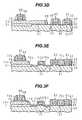
- FIGS. 3A to 3 Fare cross sectional views of a substrate illustrating a method of manufacturing a semiconductor device according to a second embodiment of the invention.
- FIGS. 4A to 4 Fare cross sectional views of a substrate illustrating a method of manufacturing a semiconductor device according to a third embodiment of the invention.
- FIGS. 5A and 5Bare cross sectional views of a substrate illustrating a method of manufacturing a semiconductor device according to a fourth embodiment of the invention.
- FIGS. 6A and 6Bare cross sectional views of a substrate illustrating a method of manufacturing a semiconductor device according to a fifth embodiment of the invention.
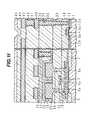
- FIGS. 1A and 1Iare cross sectional views of a substrate illustrating a method of manufacturing a semiconductor device according to the fifth embodiment.
- the left side of a cut portionshows a memory cell area
- the right sideshows an n-channel MISFET forming area in the logic circuit area.
- element separation structures 2 of a shallow trench typeare formed by a well-known method.
- the element separation structures 2define an active region 3 in the memory cell array area and an active region 4 in the logic circuit area.
- gate oxide films 7 of SiO 2are formed to a thickness of 5 to 10 nm through thermal oxidation.
- a polysilicon film 8is deposited to a thickness of 100 to 250 nm, covering the gate oxide film 7 .
- the polysilicon film 8is deposited through chemical vapor deposition (CVD) using SiH 4 .
- the polysilicon film 8is subject to a first phosphorous (P) ion implantation under the conditions of an acceleration energy of 10 to 30 keV and a dose of 3 to 6 ⁇ 10 15 cm ⁇ 2 .
- Pphosphorous
- the p-channel MISFET forming area (not shown) in the logic circuit areais covered with a resist pattern.
- the surface of the polysilicon film 8 in the logic circuit areais covered with a resist pattern 5 .
- the polysilicon film 8 in the memory cell areais subject to a second P ion implantation under the conditions of an acceleration energy of 10 to 30 keV and a dose of 5 to 8 ⁇ 10 15 cm ⁇ 2 . After this ion implantation, the resist pattern 5 is removed.
- the polysilicon film 8is patterned to leave a plurality of word lines 8 a in the memory cell area and gate electrodes 8 b in the logic circuit.
- the polysilicon film 8is etched through reactive ion etching (RIE) using a mixture gas of Cl 2 and O 2 .
- RIEreactive ion etching
- the word line 8 aextends vertically relative to the surface of the drawing sheet.
- Two word lines 8 atraverse on one active region 3 .
- the word lines 8 aare also formed on the element separation structures 2 on both sides of the active region 3 .
- the word lines 8 a on the active region 3also serve as the gate electrodes of MISFET's to be formed in the active region 3 .
- impurity ionsare implanted.
- P ionsare implanted in the MISFET forming area in the memory cell area under the conditions of an acceleration energy of 10 to 30 keV and a dose of 1 to 5 ⁇ 10 13 cm ⁇ 2 .
- P ionsare implanted in the n-channel MISFET forming area in the logic circuit area under the conditions of an acceleration energy of 5 to 30 keV and a dose of 1 to 5 ⁇ 10 13 cm ⁇ 2 , and then As ions are doped in the same area under the conditions of an acceleration energy of 5 to 30 keV and a dose of 1 to 50 ⁇ 10 13 cm ⁇ 2 .
- source/drain regions 9 a of MISFET'sare formed in the memory cell area, and low concentration regions 9 b of the source/drain regions of a lightly doped drain (LDD) structure are formed in the logic circuit area.
- LDDlightly doped drain
- a high performance MISFETcan be formed in the logic circuit area by doping As in the low concentration region 9 b of MISFET.
- the source/drain regions 9 a of MISFET in the memory cell areaare doped with only P without doping As, so that DRAM having a reduced leak current and good refresh characteristics can be formed.
- An SiO 2 filmis deposited to a thickness of 80 to 120 nm over the substrate whole surface.
- the SiO 2 filmis deposited through CVD using SiH 4 and O 2 .
- the memory cell areais covered with a resist pattern 11 to anisotropically etch the SiO 2 in the logic circuit area.
- Side wall insulating films 10 bare therefore left on the side walls of the gate electrode in the logic circuit area, and an SiO 2 film 10 a is left in the memory cell area.
- ion implantation processesare performed to form source/drain regions in the logic circuit area.
- ionsare implanted in the n-channel MISFET forming area under the conditions of an acceleration energy of 30 to 40 keV and a dose of 2 to 4 ⁇ 10 15 cm ⁇ 2
- boron (B) ionsare implanted in the p-channel MISFET forming area under the conditions of an acceleration energy of 5 to 15 keV and a dose of 2 to 4 ⁇ 10 15 cm ⁇ 2 .
- the memory cell areais covered with the resist pattern.
- high concentration regions 12 b of source/drain regions of the LDD structureare formed.
- a natural oxide film on the silicon surfaceis removed by using hydrofluoric acid.
- cobalt silicide (CoSi 1 ) films 15are formed on the surfaces of the gate electrode 8 b and high concentration regions 12 b .
- a method of forming the CoSi 2 filmwill be described in the following. First, a Co film is deposited through sputtering or the like, covering the whole surface of the substrate. A first thermal annealing is performed at a substrate temperature of 450 to 500° C., and thereafter a second thermal annealing is performed at a substrate temperature of 800 to 900° C. A silicide reaction is therefore performed between the silicon surface and CO film to thereby form the CoSi 2 film 15 . The Co film without the silicide reaction is removed by using hydrofluoric acid. In this manner, the CoSi 2 film 15 can be formed in a self-alignment manner only on the silicon exposed surface.
- the silicide reactionwill not occur in these areas. Since the high concentration regions 12 b of the source/drain regions in the logic circuit area are in contact with the Co film, the silicide reaction occurs at the interface therebetween.
- Other metals different from Comay be used which form a metal silicide through a silicide reaction with Si, such as Ti.
- a borophosphosilicate glass (BPSG) film 18is deposited to a thickness of 800 to 1200 nm, covering the whole surface of the substrate.
- the BPSG film 18is deposited through CVD using a mixture gas of SiH 4 , B 2 H 6 , O 2 , and PH 3 as source gases.
- a thermal annealingis performed at a substrate temperature of 700 to 850° C., and thereafter the surface of the BPSG film is planarized through chemical mechanical polishing (CMP).
- a contact hole 19is formed exposing the surface of the source/drain region 9 a at the center of the active region 3 , by etching the BPSG film 18 through RIE using a mixture gas of CF 4 and CHF 3 .
- a bit line 20is formed which is connected to the central source/drain region 9 a via the contact hole 19 .
- the bit line 20extends along a direction perpendicular to the word line 82 , in the area other than the cross sectional view of FIG. 1 F.
- a method of forming the bit line 20will be described in the following.
- a 50 nm thick polysilicon film doped with P and a 100 nm thick tungsten silicide (WSi) filmare deposited covering the whole surface of the substrate.
- the polysilicon filmis deposited through CVD using SiH 5 as source gas, and the WSi film is deposited through CVD using WF 6 , and SiH 4 as source gases.
- a natural oxide film formed on the bottom of the contact hole 19may be removed by using hydrofluoric acid.
- the polysilicon film and WSi filmare patterned to form the bit line 20 .
- the polysilicon film and WSi filmare etched through RIE using Cl 2 and O 2 .
- a BPSG film 23is deposited to a thickness of 800 to 1200 nm, covering the whole surface of the substrate.
- a thermal annealingis performed at a substrate temperature of 700 to 850° C., and thereafter the surface of the BPSG film 23 is planarized through CMP.
- Contact holes 24are formed exposing the surfaces of the source/drain regions 9 a on both sides the central source/drain region 9 a in the active region 3 .
- Storage electrodes 25are formed which is connected to the source/drain regions 9 a via the corresponding contact holes 24 .
- the storage electrode 25is formed by depositing a polysilicon film doped with P to a thickness of 300 to 800 nm and thereafter patterning this film.
- a silicon nitride (SiN) filmis deposited to a thickness of 3 to 5 m, covering the whole surface of the substrate.
- This SiN filmis thermally oxidized at a temperature of 700 to 800° C. to form a capacitor dielectric film 28 made of SiON.
- An opposing electrode 29 made of polysilicon doped with P and having a thickness of 100 nmis formed covering the capacitor dielectric film 28 .
- the dielectric film 28 and opposing electrode 29 in an area different from the memory cell array areaare removed. This two-layer etching is performed through RIE using Cl 2 and O 2 ⁇ .
- a BPSG film 30is deposited to a thickness of 1000 to 1500 nm, covering the whole surface of the substrate.
- Contact holes 32are formed exposing a partial surface area of the opposing electrode 29 and a partial surface area of the CoSi 2 film 15 in the logic circuit area.
- a contact hole exposing a partial surface area of the bit line 20is formed at the same time.
- the inside of the contact hole 32is embedded with a W plug 35 .
- a method of forming the W plug 35will be described in the following.
- a barrier metal layeris deposited by sputtering.
- the barrier layerhas a two-layer structure of a Ti film and a TiN film.
- a W filmis deposited through CVD to a thickness of 300 to 500 nm on the barrier metal layer to fill the inside of the contact hole 32 with W. Unnecessary W film and barrier metal layer are removed by CMP to leave only the W plug 35 in the contact hole 32 .
- a wiring pattern 40is formed on the BPSG film 30 .
- the wiring patternhas a lamination structure constituted of a barrier metal layer, an aluminum (Al) film, and an antireflection film.
- the antireflection filmis made of TiN.
- An SiO 2 film 41is deposited on the BPSG film 30 , covering the wiring pattern 40 .
- the SiO 2 film 41is deposited through CVD using high density plasma.
- a contact holeis formed in the SiO 2 film 41 and the inside of the contact hole is embedded with a W plug 42 .
- a wiring pattern 43is formed on the surface of the SiO 2 film 41 , and an SiO 2 film 44 is deposited covering the wiring pattern 43 .
- a cover film 45is deposited covering the SiO 2 film.
- the cover film 45has a two-layer structure constituted of an SiO 2 film and an SiN film both formed through plasma CVD.
- the first ion implantation illustrated in FIG. 1 A and the second ion implantation illustrated in FIG. 1Bare performed for the gate electrode of MISFET in the memory cell area, i.e., word line 8 a . Only the first ion implantation illustrated in FIG. 1A is performed for the gate electrode 8 b of n-channel MISFET in the logic circuit area.
- the gate electrodes and word linesare used as a mask in the ion implantation process for the source/drain regions described with reference to FIGS. 1C and 1D .
- impuritiesare additionally implanted into the word lines 8 a and gate electrodes 8 b .
- the doses of the first and second ion implantation processesare properly selected so that the impurity concentrations in the gate electrodes of MISFET's in the memory cell area and logic circuit area can be within adequate ranges.
- the first ion implantation illustrated in FIG. 1Ais performed for both of the memory cell area and the logic circuit area.
- ion implantationmay be performed at a dose of 8 to 15 ⁇ 10 16 cm ⁇ 2 without the first ion implantation.
- ion implantation for the gate electrode 8 bis performed at a same time when ion implantation for a source/drain region of MISFET in the logic circuit area.
- FIG. 2Ais a graph showing a relation between an impurity dose in a gate electrode and a drain current when a voltage 2.5 V is applied to the gate electrode.
- the abscissarepresents an impurity dose in the gate electrode in the unit of “ ⁇ 10 15 cm ⁇ 2 ”, and the ordinate represents a drain current represented by a value relative to 100 which is the largest drain current among samples used.
- the thickness of the gate electrodewas set to 180 nm, implanted impurities were P, and the acceleration energy of ion implantation was set to 20 keV.
- the impurity dose in the channel regionwas adjusted so that the threshold voltage became 0.45 V.
- a largest drain currentis obtained at about the impurity dose of 4 ⁇ 10 15 cm —2 .
- the drain currentreduces. This is because it is necessary to raise the impurity concentration of the channel region as the impurity concentration of the gate electrode increases, in order to prevent the threshold value from being lowered. If the impurity concentration of the gate electrode is too low, the gate electrode is depleted and the characteristics of MISFET are degraded. It is therefore preferable to set the impurity concentration of the gate electrode to about 4 ⁇ 10 15 cm ⁇ 2 .
- FIG. 2Bis a graph showing a relation between an impurity dose in the gate electrode and a sheet resistance of the gate electrode.
- the abscissarepresents an impurity dose in the gate electrode in the unit of “ ⁇ 10 15 cm ⁇ 2 ”, and the ordinate represents a sheet resistance in the unit of“ ⁇ / ⁇ ”.
- the gate electrode thickness, implanted impurities, and acceleration energywere the same as those used for the graph of FIG. 2A.
- a sheet resistance of a word line of DRAMis generally 80 ⁇ / ⁇ or lower.
- the impurity dose in the gate electrodeis set to about 1 ⁇ 10 16 cm ⁇ 2.
- the memory cell areais covered with the SiO 2 film 10 a during the silicide reaction process illustrated in FIG. 1 E. It is therefore possible to prevent a metal silicide from being formed on the surfaces of the source/drain regions in the memory cell area. The good data storage characteristics can therefore be realized.
- capacitorsare formed in the logic circuit area.
- the right side of a cut portionshows a memory cell area, and the left side shows a logic circuit area.
- element separation structures 51are formed to define active regions 3 in the memory cell array area and logic circuit area.
- gate oxide films 52are formed to a thickness of 5 to 10 nm through thermal oxidation.
- a first conductive film 53 made of polysiliconis deposited to a thickness of 100 to 250 nm over the whole surface of the substrate.
- the first conductive film 53may be made of amorphous silicon instead of polysilicon.
- P ionsare implanted into the first conductive film 53 in an n-channel MISFET forming area and a capacitor forming area in the logic circuit area, for example, under the conditions of an acceleration energy of 20 keV and a dose of 3 to 6 ⁇ 10 15 cm ⁇ 2 .
- P and Asmay be implanted at a total dose of 3 to 6 ⁇ 10 15 cm ⁇ 2 .
- Boron (B) ionsare implanted into the first conductive film 53 in a p-channel MISFET forming area in the logic circuit area. Impurities are not necessarily required to be implanted into the first conductive film 53 in the p-channel MISFET forming area.
- the gate electrode of p-channel MISFETis implanted with p-type impurities at the same time when ions are implanted for forming source/drain regions. After the above ion implantation processes, annealing is performed for activating implanted ions.
- the first conductive film 53 in the memory cell areais removed through RIE using a mixture gas of Cl 2 and O 2 .
- the gate oxide film 52 left on the surface of the memory cell area and a natural oxide film formed on the surface of the first conductive film 53are removed by using hydrofluoric acid.
- the surface of the active region in the memory cell areais thermally oxidized to form a second gate oxide film 55 having a thickness of 5 to 10 nm.
- the surface of the first conductive layer 53is also oxidized so that a capacitor dielectric film 56 having a thickness of 10 to 30 nm can be formed at the same time.
- a polysilicon film 60 , a tungsten silicide (WSi) film 61 , and a first SiN film 62are formed through CVD in this order over the whole surface of the substrate.
- the polysilicon film 60is 50 to 100 nm in thickness and doped with P to impart an n-type conductivity.
- the WSi film 61 and first SiN film 62have both a thickness of 100 to 200 nm.
- the word line 65 and capacitor upper electrode 66have both a three-layer structure constituted of the polysilicon film 60 , WSi film 61 , and first SiN film 62 .
- the first SiN film 62is etched through RIE using a mixture gas of CH 4 , CHF 3 , and Ar, the WSi film 61 is etched through RIE using a mixture gas of Cl 2 and O 2 , and the polysilicon film 60 is etched through RIE using a mixture gas of Cl 2 and O 2 .
- Source/drain regions 67are therefore formed on both side of the word line 65 in the memory cell area.
- Side wall insulating films 68 made of SiNare formed on the side walls of the word line 65 and capacitor upper electrode 66 .
- the side wall insulating film 68is formed by depositing an SiN film over the whole surface of the substrate and anisotropically etching this film. This anisotropic etching is performed through RIE using a mixture gas of CF 4 , CHF 3 , and Ar. In this case, the capacitor dielectric film 56 on the first conductive film 53 in the area where the upper capacitor electrode 66 is not formed, is also removed and the upper surface of the first conductive film 53 is exposed.
- the first conductive film 53is patterned to leave a lower capacitor electrode 53 a in an area inclusive of the upper capacitor electrode 66 as viewed along a direction normal to the substrate surface and to leave a gate electrode 53 b in the n-channel MISFET forming area in the logic circuit area.
- the gate electrodeis also left in the p-channel MISFET forming area.
- the first conductive film 53is etched through RIE using a mixture gas of Cl 2 and O 2 .
- the side wall insulating film 68 on the side wall of the first conductive film 53is left without being removed. In such a case, when the first conductive film 53 is etched, the boarder area of the first conductive film 53 is covered with a mask pattern to positively leave the first conductive film 53 under the mask pattern.
- the ion implantation conditionsare an acceleration energy of 5 to 15 keV and a dose of 1 to 10 ⁇ 10 13 cm ⁇ 2 .
- B ionsare implanted in the p-channel MISFET forming area under the ion implantation conditions of an acceleration energy of 5 to 15 keV and a dose of 1 to 10 ⁇ 10 13 cm ⁇ 2 .
- SiO 2 filmis deposited over the whole surface of the substrate and anisotropically etched to leave side wall insulating films 70 b on the side walls of the gate electrode 53 a .
- side wall insulating films 70 aare left on the side walls of the lower capacitor electrode 53 a
- side wall insulating films 70 dare left on the slanted surfaces of the side wall insulating films 68 .
- spaces between word lines 65are embedded with embedding insulating members 70 c.
- ionsare implanted in the n-channel MISFET forming area in the logic circuit area for forming high concentration regions of the LDD structure.
- the ion implantation conditionsare an acceleration energy of 30 to 40 keV and a dose of 2 to 4 ⁇ 10 15 cm ⁇ 2 .
- B ionsare implanted in the p-channel MISFET forming area (not shown) under the ion implantation conditions of an acceleration energy of 5 to 15 keV and a dose of 2 to 4 ⁇ 10 15 cm ⁇ 2 .
- annealing for activationis performed to thus form source/drain regions 71 of the LDD structure.
- CoSi 2 films 72are formed on the upper surfaces of the source/drain regions 71 and gate electrode 53 b of MISFET in the logic circuit area.
- the CoSi 2 film 72is formed by a process similar to the process of forming the CoSi 2 film 15 of the first embodiment described with reference to FIG. 1 E. During this process, since the surfaces of the source/drain regions 67 in the memory cell area are covered with the embedding insulating members 70 c , the CoSi 2 film is not formed on the surfaces of the source/drain regions 67 .
- DRAM mixed with logic circuits and containing a capacitoris formed, the capacitor being constituted of the lower capacitor electrode 53 a , capacitor dielectric film 56 , and upper capacitor electrode 66 .
- a metal silicide filmcan be formed only in the logic circuit area without forming it in the logic circuit area.
- the upper capacitor electrode 66is formed by the same process as that for the word lines 65 in the memory cell area
- the lower capacitor electrode 53 ais formed by the same process as that for the gate electrode 53 b in the logic circuit area. Therefore, a capacitor having a lamination structure of a polysilicon film/an SiO 2 film/a polysilicon film can be formed by suppressing an increase in the number of manufacture processes as much as possible.
- the top and side surfaces of the word line 65are covered with the side wall insulating films 68 made of SiN and first SiN film 62 .
- These side wall insulating films 68 and first SiN film 62function as the protective films for the WSi film 61 and polysilicon film 60 if the contact hole 19 shown in FIG. 1 F and the contact hole 24 shown in FIG. 1G are formed under the conditions that SiN is not substantially etched It is therefore possible to form the contact holes 19 and 24 in a self-alignment manner.
- the side wall insulating films 70 b on the side walls of the gate electrode 53 b in the logic circuit areaare made of SiO 2 , it is possible to enhance a hot carrier resistance of MISFET and reduce parasitic capacitance more than the case where the side wall insulating films are made of SiN. Since the side wall insulating films 70 b are formed by a process different from the process of forming the side wall insulating films 68 in the memory cell area, it is possible to set the thickness of the side wall insulating film 70 b to a value most suitable for suppressing the short channel effects.
- FIG. 4Acorresponds to FIG. 1C of the first embodiment.
- a different point from the first embodimentis that an upper SiO 2 film 80 of about 100 nm thickness is formed on the word line 8 a .
- Processes up to the process illustrated in FIG. 4Awill be described by paying attention to processes different from those up to FIG. 1 C.
- a polysilicon film and an SiO 2 filmare deposited, and the SiO 2 film in the logic circuit is removed. Similar to the first embodiment, the polysilicon film contains implanted ions. After the SiO 2 film in the logic circuit area is removed, the processes similar to the first embodiment are performed to form the substrate shown in FIG. 4 A.
- ions implanted for forming low density regions 9 b of MISFET in the logic circuit areaions are implanted for forming source/drain regions 9 a in the memory cell area.
- CoSi 2 films 15are therefore formed on the upper surface of the gate electrode 8 b in the logic circuit area and on the upper surfaces of high concentration regions 12 b of the source/drain regions.
- the memory cell areais being covered with an SiO 2 film which has a thickness of 50 to 120 nm.
- a low temperature SiO 2 film 81is deposited to a thickness of 20 to 50 nm over the whole surface of the substrate.
- the low temperature SiO 2 , film 81is deposited through CVD at a growth temperature of 700° C. or lower.
- the SiO 2 film 81is deposited through plasma CVD at a substrate temperature of about 400° C. Deposition at a low temperature can prevent the CoSi 2 film 15 from being deteriorated by heat.
- the SiO 2 film 10 a and low temperature SiO 2 film 81are anisotropically etched to leave side wall insulating films 82 on the side walls of the lamination structures in the memory cell area each constituted of the word line 8 a and upper SiO 2 film 80 .
- the logic circuit areais covered with a resist pattern.
- the low temperature SiO 2 film 81 in the logic circuit areais left unetched.
- An amorphous silicon film doped with Pis deposited through CVD to a thickness of 100 to 200 nm over the whole surface of the substrate.
- the amorphous silicon filmis patterned to leave pads 83 on the source/drain regions 9 a in the memory cell area.
- the pad 83covers the surface of the source/drain region 9 a , the side surfaces of the side wall insulating films 82 on both sides of the source/drain region 9 a , and partial top surfaces of the upper SiO 2 films 80 .
- a BPSG film 18is deposited over the whole surface of the substrate, and a contact hole 19 is formed therein. Thereafter, a bit line 20 is formed which contacts the pad 83 .
- a BPSG film 23is deposited over the substrate whole surface, a contact hole 24 is formed and thereafter a storage electrode 25 is formed.
- the pads 83are exposed at the bottoms of the contact holes.
- the source/drain regions 9 aare not exposed therefore directly to the etching atmosphere, so that any defect in the source/drain regions 9 a can be prevented from being formed. It is therefore possible to prevent the data storage characteristics of DRAM from being deteriorated by defects in the source/drain regions 9 a.
- MISFET's in the memory cell area and logic circuit areaare formed generally in parallel.
- a method of forming DRAM formed with logic circuitsis known by which after all constituents up to an opposing electrode (e.g., opposing electrode 29 shown in FIG. 1H ) are formed in the memory cell area, source/drain regions of MISFET in the logic circuit area are formed.
- a problem associated with this methodis how a bit line in the memory cell area is electrically connected to a wiring pattern in the logic circuit area.
- Fourth and fifth embodiments to be described hereinafterfeature in this connection structure.
- FIGS. 5A and 5Bare cross sectional views of the boundary areas between the memory cell area and logic circuit area.
- MISFET's 91As shown in FIG. 5A , formed in the memory cell area (approximately a right half area of FIG. 5A ) of a silicon substrate 90 are MISFET's 91 , word lines 92 , an interlayer insulating film 98 , a bit line 93 , an interlayer insulating film 99 , storage electrodes 94 , capacitor dielectric films 95 , and an opposing electrode 96 .
- This configurationcan be formed by processes similar to those shown in FIGS. 1A to 1 H. However, in the logic circuit area, only gate electrodes are formed, and the ion implantation for high concentration regions 12 b of source/drain regions shown in FIG. 1 D and the formation of the CoSi 2 15 shown in FIG. 1E are not performed. In the logic circuit area, a gate electrode 100 and side wall insulating films 101 on the side walls of the gate electrode 100 are formed. The interlayer insulating films 98 and 00 and opposing electrode 96 are also formed in the logic circuit
- a resist pattern 97is formed covering the surface of the opposing electrode 96 in the memory cell area.
- the boarder of the resist patternprotrudes toward the logic circuit area by about 0.2 ⁇ m from the front end of the bit line 93 .
- the opposing electrode 96 deposited in the logic circuitis removed.
- the opposing electrode 96is removed thorough isotropic etching using chlorine containing gas.
- the opposing electrode 96is also side-etched and the boarder thereof retracts from the boarder of the resist pattern 97 .
- the depth of side-etchis set to about 1 to 1.5 ⁇ m. Namely, the border of the opposing electrode 96 retracts from the front-end of the bit line 93 by about 0.8 to 1.3 ⁇ m.
- the interlayer insulating films 99 and 98 in the logic circuit areaare removed by using the resist pattern 97 as a mask.
- the interlayer insulating films 99 and 98are removed through anisotropic RIE.
- anisotropic RIEthe surfaces of the gate electrode 100 , side wall insulating films 101 , and silicon substrate 90 may be covered with a thin SiN film. If this thin SiN film is used, it is removed after the interlayer insulating films 99 and 98 are removed.
- P ionsare implanted in the logic circuit area by using as a mask the gate electrode 100 and side wall insulating films 101 .
- the ion implantation conditionsare the same as those used for forming the high concentration regions 12 b of the first embodiment shown in FIG. 1 D. After this ion implantation, the resist pattern 97 is removed.
- an interlayer insulating film 105 of BPSGis deposited over the substrate whole surface, and the surface thereof is planarized through CMP.
- a contact hole 106is formed thorough the interlayer insulating films 105 and 99 to expose the partial top surface of the bit line 93 .
- the contact hole 106is formed at the position away from the boarder of the opposing electrode 96 toward the logic circuit area. Since the boarder of the opposing electrode 96 retracts by about 0.8 to 1.3 ⁇ m from the front end of the bit line 93 , the contact hole 106 can be formed without being in contact with the opposing electrode 93 .
- a wiring pattern 107is formed on the interlayer insulating film 105 . This wiring pattern 107 is connected via the contact hole 106 to the bit line 93 .
- the boarder of the opposing electrode 96is defined by side-etch, and a dedicated photomask for defining the boarder of the opposing electrode 96 is not used.
- the boarder of the opposing electrode 96can be, defined by using only the resist pattern which defines the boarder line between the memory cell area and logic circuit area.
- the memory cell area of a silicon substrate 90has a DRAM circuit formed therein.
- the structure of the DRAM circuitis the same as that of the fourth embodiment shown in FIG. 5 A.
- An element separation structure 110defines a boarder between the memory cell area and logic circuit area.
- an interconnect wiring pattern 111is formed in correspondence with each bit line 93 .
- the interconnect wiring pattern 111is formed by the same processes as those used for a word line 92 .
- Each bit line 93is connected to the interconnect wiring pattern 110 via a contact hole formed through an interlayer insulating film 98 at the position near the front end of the bit line 93 .
- the surface of an opposing electrode 96 in the memory cell areais covered with a resist pattern 97 .
- the opposing electrode 96 and interlayer insulating film 99 in the logic circuit areaare removed.
- a partial surface area of the interconnect wiring pattern 111is exposed in the logic circuit area.
- the surfaces of the gate electrode 100 , side wall insulating films 101 , and interconnect wiring pattern 111may be covered with an SiN film which is used as an etching stopper layer. Similar to the processes of the fourth embodiment shown in FIG. 5A , P ions are implanted in the logic circuit area.
- an interlayer insulating film 105 of BPSGis deposited over the substrate whole surface, and the surface thereof is planarized through CMP.
- a contact hole 106is formed thorough the interlayer insulating film 105 to expose the partial top surface of the interconnect wiring pattern 111 .
- the contact hole 106is formed at the position away from the boarder of the opposing electrode 96 toward the logic circuit area. Since the interconnect wiring pattern 111 extends to the logic circuit area, the contact hole 106 can be formed without being in contact with the opposing electrode 93 .
- a wiring pattern 107is formed on the interlayer insulating film 105 . This wiring pattern 17 is connected via the contact hole 106 to the bit line 93 .
- the bit line 93is connected to the wiring pattern 107 via the interconnect wiring pattern 111 . Therefore, similar to the fourth embodiment, the bit line 93 and wiring pattern 107 can be connected with good reproductivity by using only the, resist pattern 97 which defines the boarder between the logic circuit area and memory cell area.
Landscapes
- Engineering & Computer Science (AREA)
- Physics & Mathematics (AREA)
- Manufacturing & Machinery (AREA)
- Condensed Matter Physics & Semiconductors (AREA)
- General Physics & Mathematics (AREA)
- Computer Hardware Design (AREA)
- Microelectronics & Electronic Packaging (AREA)
- Power Engineering (AREA)
- High Energy & Nuclear Physics (AREA)
- Health & Medical Sciences (AREA)
- Toxicology (AREA)
- Semiconductor Memories (AREA)
Abstract
Description
Claims (4)
Priority Applications (2)
| Application Number | Priority Date | Filing Date | Title |
|---|---|---|---|
| US09/961,264US6987041B2 (en) | 1998-10-02 | 2001-09-25 | Semiconductor device having both memory and logic circuit and its manufacture |
| US11/186,810US7429507B2 (en) | 1998-10-02 | 2005-07-22 | Semiconductor device having both memory and logic circuit and its manufacture |
Applications Claiming Priority (4)
| Application Number | Priority Date | Filing Date | Title |
|---|---|---|---|
| JPHEI10-281699 | 1998-10-02 | ||
| JP28169998AJP4199338B2 (en) | 1998-10-02 | 1998-10-02 | Semiconductor device and manufacturing method thereof |
| US09/288,302US6326657B1 (en) | 1998-02-10 | 1999-04-08 | Semiconductor device having both memory and logic circuit and its manufacture |
| US09/961,264US6987041B2 (en) | 1998-10-02 | 2001-09-25 | Semiconductor device having both memory and logic circuit and its manufacture |
Related Parent Applications (1)
| Application Number | Title | Priority Date | Filing Date |
|---|---|---|---|
| US09/288,302DivisionUS6326657B1 (en) | 1998-02-10 | 1999-04-08 | Semiconductor device having both memory and logic circuit and its manufacture |
Related Child Applications (1)
| Application Number | Title | Priority Date | Filing Date |
|---|---|---|---|
| US11/186,810DivisionUS7429507B2 (en) | 1998-10-02 | 2005-07-22 | Semiconductor device having both memory and logic circuit and its manufacture |
Publications (2)
| Publication Number | Publication Date |
|---|---|
| US20020011619A1 US20020011619A1 (en) | 2002-01-31 |
| US6987041B2true US6987041B2 (en) | 2006-01-17 |
Family
ID=17642757
Family Applications (3)
| Application Number | Title | Priority Date | Filing Date |
|---|---|---|---|
| US09/288,302Expired - LifetimeUS6326657B1 (en) | 1998-02-10 | 1999-04-08 | Semiconductor device having both memory and logic circuit and its manufacture |
| US09/961,264Expired - LifetimeUS6987041B2 (en) | 1998-10-02 | 2001-09-25 | Semiconductor device having both memory and logic circuit and its manufacture |
| US11/186,810Expired - Fee RelatedUS7429507B2 (en) | 1998-10-02 | 2005-07-22 | Semiconductor device having both memory and logic circuit and its manufacture |
Family Applications Before (1)
| Application Number | Title | Priority Date | Filing Date |
|---|---|---|---|
| US09/288,302Expired - LifetimeUS6326657B1 (en) | 1998-02-10 | 1999-04-08 | Semiconductor device having both memory and logic circuit and its manufacture |
Family Applications After (1)
| Application Number | Title | Priority Date | Filing Date |
|---|---|---|---|
| US11/186,810Expired - Fee RelatedUS7429507B2 (en) | 1998-10-02 | 2005-07-22 | Semiconductor device having both memory and logic circuit and its manufacture |
Country Status (4)
| Country | Link |
|---|---|
| US (3) | US6326657B1 (en) |
| JP (1) | JP4199338B2 (en) |
| KR (1) | KR100320332B1 (en) |
| TW (1) | TW410464B (en) |
Cited By (41)
| Publication number | Priority date | Publication date | Assignee | Title |
|---|---|---|---|---|
| US20070257291A1 (en)* | 2006-05-02 | 2007-11-08 | Serguei Okhonin | Semiconductor memory cell and array using punch-through to program and read same |
| US20070297252A1 (en)* | 2006-06-26 | 2007-12-27 | Anant Pratap Singh | Integrated circuit having memory array including ECC and/or column redundancy, and method of programming, controlling and/or operating same |
| US20080180995A1 (en)* | 2007-01-26 | 2008-07-31 | Serguei Okhonin | Semiconductor Device With Electrically Floating Body |
| US20080237714A1 (en)* | 2007-03-29 | 2008-10-02 | Pierre Fazan | Manufacturing Process for Zero-Capacitor Random Access Memory Circuits |
| US20080298139A1 (en)* | 2007-05-30 | 2008-12-04 | David Fisch | Integrated circuit having voltage generation circuitry for memory cell array, and method of operating and /or controlling same |
| US20090080244A1 (en)* | 2007-09-17 | 2009-03-26 | Eric Carman | Refreshing Data of Memory Cells with Electrically Floating Body Transistors |
| US20090141550A1 (en)* | 2006-04-07 | 2009-06-04 | Eric Carman | Memory Array Having a Programmable Word Length, and Method of Operating Same |
| US20090146219A1 (en)* | 2007-12-11 | 2009-06-11 | Danngis Liu | Integrated circuit having memory cell array, and method of manufacturing same |
| US20090200612A1 (en)* | 2008-02-08 | 2009-08-13 | Viktor Koldiaev | Integrated Circuit Having Memory Cells Including Gate Material Having High Work Function, and Method of Manufacturing Same |
| US20090231898A1 (en)* | 2006-07-11 | 2009-09-17 | David Fisch | Integrated Circuit Including Memory Array Having a Segmented Bit Line Architecture and Method of Controlling and/or Operating Same |
| US20090251958A1 (en)* | 2008-04-04 | 2009-10-08 | Philippe Bauser | Read circuitry for an integrated circuit having memory cells and/or a memory cell array, and method of operating same |
| US20100075471A1 (en)* | 2008-09-25 | 2010-03-25 | Innovative Silicon Isi Sa | Recessed Gate Silicon-On-Insulator Floating Body Device With Self-Aligned Lateral Isolation |
| US20100085806A1 (en)* | 2008-10-02 | 2010-04-08 | Ping Wang | Techniques for reducing a voltage swing |
| US20100091586A1 (en)* | 2008-10-15 | 2010-04-15 | Innovative Silicon Isi Sa | Techniques for simultaneously driving a plurality of source lines |
| US20100110816A1 (en)* | 2008-11-05 | 2010-05-06 | Innovative Silicon Isi Sa | Techniques for block refreshing a semiconductor memory device |
| US20100210075A1 (en)* | 2009-02-18 | 2010-08-19 | Innovative Silicon Isi Sa | Techniques for providing a source line plane |
| US20100224924A1 (en)* | 2009-03-04 | 2010-09-09 | Innovative Silicon Isi Sa | Techniques for forming a contact to a buried diffusion layer in a semiconductor memory device |
| US20100259964A1 (en)* | 2009-03-31 | 2010-10-14 | Innovative Silicon Isi Sa | Techniques for providing a semiconductor memory device |
| US20100271857A1 (en)* | 2009-04-27 | 2010-10-28 | Innovative Silicon Isi Sa | Techniques for providing a direct injection semiconductor memory device |
| US20100277982A1 (en)* | 2009-04-30 | 2010-11-04 | Innovative Silicon Isi Sa | Semiconductor device with floating gate and electrically floating body |
| US20110007578A1 (en)* | 2009-07-10 | 2011-01-13 | Innovative Silicon Isi Sa | Techniques for providing a semiconductor memory device |
| US20110019481A1 (en)* | 2009-07-27 | 2011-01-27 | Innovative Silicon Isi Sa | Techniques for providing a direct injection semiconductor memory device |
| US20110058436A1 (en)* | 2009-09-04 | 2011-03-10 | Innovative Silicon Isi Sa | Techniques for sensing a semiconductor memory device |
| US20110141836A1 (en)* | 2009-12-16 | 2011-06-16 | Innovative Silicon Isi Sa | Techniques for reducing impact of array disturbs in a semiconductor memory device |
| US20110199848A1 (en)* | 2010-02-12 | 2011-08-18 | Innovative Silicon Isi Sa | Techniques for controlling a semiconductor memory device |
| US8014195B2 (en) | 2008-02-06 | 2011-09-06 | Micron Technology, Inc. | Single transistor memory cell |
| US20110216617A1 (en)* | 2010-03-04 | 2011-09-08 | Innovative Silicon Isi Sa | Techniques for sensing a semiconductor memory device |
| US20110216608A1 (en)* | 2010-03-05 | 2011-09-08 | Innovative Silicon Isi Sa | Techniques for reading from and/or writing to a semiconductor memory device |
| US20110216605A1 (en)* | 2010-03-04 | 2011-09-08 | Innovative Silicon Isi Sa | Techniques for providing a semiconductor memory device having hierarchical bit lines |
| US8085594B2 (en) | 2007-06-01 | 2011-12-27 | Micron Technology, Inc. | Reading technique for memory cell with electrically floating body transistor |
| US8174881B2 (en) | 2009-11-24 | 2012-05-08 | Micron Technology, Inc. | Techniques for reducing disturbance in a semiconductor device |
| US8213226B2 (en) | 2008-12-05 | 2012-07-03 | Micron Technology, Inc. | Vertical transistor memory cell and array |
| US8411524B2 (en) | 2010-05-06 | 2013-04-02 | Micron Technology, Inc. | Techniques for refreshing a semiconductor memory device |
| US8498157B2 (en) | 2009-05-22 | 2013-07-30 | Micron Technology, Inc. | Techniques for providing a direct injection semiconductor memory device |
| US8531878B2 (en) | 2011-05-17 | 2013-09-10 | Micron Technology, Inc. | Techniques for providing a semiconductor memory device |
| US8536628B2 (en) | 2007-11-29 | 2013-09-17 | Micron Technology, Inc. | Integrated circuit having memory cell array including barriers, and method of manufacturing same |
| US8547738B2 (en) | 2010-03-15 | 2013-10-01 | Micron Technology, Inc. | Techniques for providing a semiconductor memory device |
| US8766356B2 (en) | 2007-09-18 | 2014-07-01 | Samsung Electronics Co., Ltd. | Semiconductor devices having bit line insulating capping patterns and multiple conductive patterns thereon |
| US8773933B2 (en) | 2012-03-16 | 2014-07-08 | Micron Technology, Inc. | Techniques for accessing memory cells |
| US8873283B2 (en) | 2005-09-07 | 2014-10-28 | Micron Technology, Inc. | Memory cell and memory cell array having an electrically floating body transistor, and methods of operating same |
| US9559216B2 (en) | 2011-06-06 | 2017-01-31 | Micron Technology, Inc. | Semiconductor memory device and method for biasing same |
Families Citing this family (17)
| Publication number | Priority date | Publication date | Assignee | Title |
|---|---|---|---|---|
| US6838320B2 (en)* | 2000-08-02 | 2005-01-04 | Renesas Technology Corp. | Method for manufacturing a semiconductor integrated circuit device |
| KR100317434B1 (en)* | 1998-03-12 | 2001-12-22 | 아끼구사 나오유끼 | Semiconductor device and manufacturing method of the same |
| US6632292B1 (en)* | 1998-03-13 | 2003-10-14 | Semitool, Inc. | Selective treatment of microelectronic workpiece surfaces |
| KR100640574B1 (en)* | 2000-11-30 | 2006-10-31 | 삼성전자주식회사 | Manufacturing Method of Semiconductor Memory Device |
| KR100390901B1 (en)* | 2000-12-28 | 2003-07-10 | 주식회사 하이닉스반도체 | Method for manufactruing transistor in sram device |
| JP4759819B2 (en)* | 2001-03-05 | 2011-08-31 | ソニー株式会社 | Manufacturing method of semiconductor device |
| JP2003031684A (en)* | 2001-07-11 | 2003-01-31 | Hitachi Ltd | Semiconductor integrated circuit device and method of manufacturing the same |
| US20030181922A1 (en)* | 2002-03-20 | 2003-09-25 | Spiration, Inc. | Removable anchored lung volume reduction devices and methods |
| US6709926B2 (en)* | 2002-05-31 | 2004-03-23 | International Business Machines Corporation | High performance logic and high density embedded dram with borderless contact and antispacer |
| DE10314595B4 (en)* | 2003-03-31 | 2006-05-04 | Infineon Technologies Ag | Method for producing transistors of different conduction type and different packing density in a semiconductor substrate |
| DE102005046734B4 (en)* | 2005-09-29 | 2011-06-16 | Infineon Technologies Ag | Semiconductor device with integrated capacitance structure |
| TWI297931B (en)* | 2006-01-11 | 2008-06-11 | Ind Tech Res Inst | Cylindrical capacitor and method of manufacturing the same |
| US7964514B2 (en)* | 2006-03-02 | 2011-06-21 | Applied Materials, Inc. | Multiple nitrogen plasma treatments for thin SiON dielectrics |
| US7419871B2 (en)* | 2006-04-25 | 2008-09-02 | Micron Technology, Inc. | Methods of forming semiconductor constructions |
| KR100840651B1 (en)* | 2006-12-29 | 2008-06-24 | 동부일렉트로닉스 주식회사 | Ion implantation method of high voltage device |
| KR101096033B1 (en)* | 2009-06-26 | 2011-12-19 | 주식회사 하이닉스반도체 | Method for fabricating semiconductor device |
| KR101800441B1 (en)* | 2010-10-22 | 2017-11-22 | 삼성전자주식회사 | Method Of Forming Semiconductor Devices |
Citations (20)
| Publication number | Priority date | Publication date | Assignee | Title |
|---|---|---|---|---|
| US5194924A (en) | 1984-05-23 | 1993-03-16 | Hitachi, Ltd. | Semiconductor device of an LDD structure having a floating gate |
| US5237187A (en) | 1990-11-30 | 1993-08-17 | Hitachi, Ltd. | Semiconductor memory circuit device and method for fabricating same |
| JPH05226593A (en) | 1992-02-12 | 1993-09-03 | Toshiba Corp | Manufacture of semiconductor device |
| US5324680A (en)* | 1991-05-22 | 1994-06-28 | Samsung Electronics, Co. Ltd. | Semiconductor memory device and the fabrication method thereof |
| US5329482A (en)* | 1991-10-07 | 1994-07-12 | Sony Corporation | Semiconductor memory device and method for producing it |
| JPH0799236A (en) | 1993-09-27 | 1995-04-11 | Sony Corp | Manufacture of semiconductor device |
| US5444653A (en) | 1993-04-26 | 1995-08-22 | Sanyo Electric Co., Ltd. | Semiconductor memory device with stack type memory cell |
| JPH07297393A (en) | 1994-04-25 | 1995-11-10 | Seiko Instr Inc | Semiconductor device and manufacture thereof |
| JPH09181269A (en) | 1995-12-26 | 1997-07-11 | Nec Corp | Manufacture of semiconductor device |
| JPH10247725A (en) | 1997-03-05 | 1998-09-14 | Mitsubishi Electric Corp | Semiconductor device and manufacturing method thereof |
| JPH10256511A (en) | 1997-03-12 | 1998-09-25 | Lg Semicon Co Ltd | Method for manufacturing semiconductor device |
| US5917211A (en) | 1988-09-19 | 1999-06-29 | Hitachi, Ltd. | Semiconductor integrated circuit, method of fabricating the same and apparatus for fabricating the same |
| US5986320A (en) | 1998-03-10 | 1999-11-16 | Mitsubishi Denki Kabushiki Kaisha | Semiconductor integrated circuit device |
| US5986309A (en) | 1991-05-30 | 1999-11-16 | Kabushiki Kaisha Toshiba | Semiconductor integrated circuit apparatus having a plurality of well bias voltage supply circuits |
| US6066881A (en)* | 1998-01-29 | 2000-05-23 | Mitsubishi Denki Kabushiki Kaisha | Integrated circuit having a memory cell transistor with a gate oxide layer which is thicker than the gate oxide layer of a peripheral circuit transistor |
| US6133599A (en) | 1998-04-01 | 2000-10-17 | Vanguard International Semiconductor Corporation | Design and a novel process for formation of DRAM bit line and capacitor node contacts |
| US6144079A (en) | 1996-04-01 | 2000-11-07 | Mitsubishi Denki Kabushiki Kaisha | Semiconductor device and method of manufacturing the same |
| US6153903A (en) | 1997-04-18 | 2000-11-28 | Micron Technology, Inc. | Cell capacitors, memory cells, memory arrays, and method of fabrication |
| US6171942B1 (en) | 1998-06-05 | 2001-01-09 | Samsung Electronics Co., Ltd. | Methods of forming electrically conductive lines in integrated circuit memories using self-aligned silicide blocking layers |
| US6414375B1 (en)* | 1998-08-20 | 2002-07-02 | Fujitsu Limited | Semiconductor device with metal silicide film on partial area of substrate surface and its manufacture method |
Family Cites Families (5)
| Publication number | Priority date | Publication date | Assignee | Title |
|---|---|---|---|---|
| US5500387A (en)* | 1994-02-16 | 1996-03-19 | Texas Instruments Incorporated | Method of making high performance capacitors and/or resistors for integrated circuits |
| KR100215845B1 (en)* | 1997-03-17 | 1999-08-16 | 구본준 | Semiconductor device manufacturing method |
| US6815295B1 (en)* | 1997-05-14 | 2004-11-09 | Renesas Technology Corp. | Method of manufacturing field effect transistors |
| US5953599A (en)* | 1997-06-12 | 1999-09-14 | National Semiconductor Corporation | Method for forming low-voltage CMOS transistors with a thin layer of gate oxide and high-voltage CMOS transistors with a thick layer of gate oxide |
| US7538384B2 (en)* | 2005-12-05 | 2009-05-26 | Taiwan Semiconductor Manufacturing Company, Ltd. | Non-volatile memory array structure |
- 1998
- 1998-10-02JPJP28169998Apatent/JP4199338B2/ennot_activeExpired - Lifetime
- 1999
- 1999-03-31TWTW088105118Apatent/TW410464B/ennot_activeIP Right Cessation
- 1999-04-08USUS09/288,302patent/US6326657B1/ennot_activeExpired - Lifetime
- 1999-04-27KRKR1019990015044Apatent/KR100320332B1/ennot_activeExpired - Lifetime
- 2001
- 2001-09-25USUS09/961,264patent/US6987041B2/ennot_activeExpired - Lifetime
- 2005
- 2005-07-22USUS11/186,810patent/US7429507B2/ennot_activeExpired - Fee Related
Patent Citations (21)
| Publication number | Priority date | Publication date | Assignee | Title |
|---|---|---|---|---|
| US5194924A (en) | 1984-05-23 | 1993-03-16 | Hitachi, Ltd. | Semiconductor device of an LDD structure having a floating gate |
| US5917211A (en) | 1988-09-19 | 1999-06-29 | Hitachi, Ltd. | Semiconductor integrated circuit, method of fabricating the same and apparatus for fabricating the same |
| US5237187A (en) | 1990-11-30 | 1993-08-17 | Hitachi, Ltd. | Semiconductor memory circuit device and method for fabricating same |
| US5324680A (en)* | 1991-05-22 | 1994-06-28 | Samsung Electronics, Co. Ltd. | Semiconductor memory device and the fabrication method thereof |
| US5986309A (en) | 1991-05-30 | 1999-11-16 | Kabushiki Kaisha Toshiba | Semiconductor integrated circuit apparatus having a plurality of well bias voltage supply circuits |
| US5329482A (en)* | 1991-10-07 | 1994-07-12 | Sony Corporation | Semiconductor memory device and method for producing it |
| JPH05226593A (en) | 1992-02-12 | 1993-09-03 | Toshiba Corp | Manufacture of semiconductor device |
| US5444653A (en) | 1993-04-26 | 1995-08-22 | Sanyo Electric Co., Ltd. | Semiconductor memory device with stack type memory cell |
| JPH0799236A (en) | 1993-09-27 | 1995-04-11 | Sony Corp | Manufacture of semiconductor device |
| JPH07297393A (en) | 1994-04-25 | 1995-11-10 | Seiko Instr Inc | Semiconductor device and manufacture thereof |
| JPH09181269A (en) | 1995-12-26 | 1997-07-11 | Nec Corp | Manufacture of semiconductor device |
| US6144079A (en) | 1996-04-01 | 2000-11-07 | Mitsubishi Denki Kabushiki Kaisha | Semiconductor device and method of manufacturing the same |
| JPH10247725A (en) | 1997-03-05 | 1998-09-14 | Mitsubishi Electric Corp | Semiconductor device and manufacturing method thereof |
| US6492690B2 (en)* | 1997-03-05 | 2002-12-10 | Mitsubishi Denki Kabushiki Kaisha | Semiconductor device having control electrodes with different impurity concentrations |
| JPH10256511A (en) | 1997-03-12 | 1998-09-25 | Lg Semicon Co Ltd | Method for manufacturing semiconductor device |
| US6153903A (en) | 1997-04-18 | 2000-11-28 | Micron Technology, Inc. | Cell capacitors, memory cells, memory arrays, and method of fabrication |
| US6066881A (en)* | 1998-01-29 | 2000-05-23 | Mitsubishi Denki Kabushiki Kaisha | Integrated circuit having a memory cell transistor with a gate oxide layer which is thicker than the gate oxide layer of a peripheral circuit transistor |
| US5986320A (en) | 1998-03-10 | 1999-11-16 | Mitsubishi Denki Kabushiki Kaisha | Semiconductor integrated circuit device |
| US6133599A (en) | 1998-04-01 | 2000-10-17 | Vanguard International Semiconductor Corporation | Design and a novel process for formation of DRAM bit line and capacitor node contacts |
| US6171942B1 (en) | 1998-06-05 | 2001-01-09 | Samsung Electronics Co., Ltd. | Methods of forming electrically conductive lines in integrated circuit memories using self-aligned silicide blocking layers |
| US6414375B1 (en)* | 1998-08-20 | 2002-07-02 | Fujitsu Limited | Semiconductor device with metal silicide film on partial area of substrate surface and its manufacture method |
Cited By (124)
| Publication number | Priority date | Publication date | Assignee | Title |
|---|---|---|---|---|
| US8873283B2 (en) | 2005-09-07 | 2014-10-28 | Micron Technology, Inc. | Memory cell and memory cell array having an electrically floating body transistor, and methods of operating same |
| US10418091B2 (en) | 2005-09-07 | 2019-09-17 | Ovonyx Memory Technology, Llc | Memory cell and memory cell array having an electrically floating body transistor, and methods of operating same |
| US11031069B2 (en) | 2005-09-07 | 2021-06-08 | Ovonyx Memory Technology, Llc | Memory cell and memory cell array having an electrically floating body transistor, and methods of operating same |
| US20090141550A1 (en)* | 2006-04-07 | 2009-06-04 | Eric Carman | Memory Array Having a Programmable Word Length, and Method of Operating Same |
| US7940559B2 (en) | 2006-04-07 | 2011-05-10 | Micron Technology, Inc. | Memory array having a programmable word length, and method of operating same |
| US8134867B2 (en) | 2006-04-07 | 2012-03-13 | Micron Technology, Inc. | Memory array having a programmable word length, and method of operating same |
| US20110194363A1 (en)* | 2006-05-02 | 2011-08-11 | Micron Technology, Inc. | Semiconductor memory cell and array using punch-through to program and read same |
| US7933142B2 (en) | 2006-05-02 | 2011-04-26 | Micron Technology, Inc. | Semiconductor memory cell and array using punch-through to program and read same |
| US8295078B2 (en) | 2006-05-02 | 2012-10-23 | Micron Technology, Inc. | Semiconductor memory cell and array using punch-through to program and read same |
| US20070257291A1 (en)* | 2006-05-02 | 2007-11-08 | Serguei Okhonin | Semiconductor memory cell and array using punch-through to program and read same |
| US8402326B2 (en) | 2006-06-26 | 2013-03-19 | Micron Technology, Inc. | Integrated circuit having memory array including ECC and column redundancy and method of operating same |
| US8069377B2 (en) | 2006-06-26 | 2011-11-29 | Micron Technology, Inc. | Integrated circuit having memory array including ECC and column redundancy and method of operating the same |
| US20070297252A1 (en)* | 2006-06-26 | 2007-12-27 | Anant Pratap Singh | Integrated circuit having memory array including ECC and/or column redundancy, and method of programming, controlling and/or operating same |
| US8395937B2 (en) | 2006-07-11 | 2013-03-12 | Micron Technology, Inc. | Integrated circuit including memory array having a segmented bit line architecture and method of controlling and/or operating same |
| US20090231898A1 (en)* | 2006-07-11 | 2009-09-17 | David Fisch | Integrated Circuit Including Memory Array Having a Segmented Bit Line Architecture and Method of Controlling and/or Operating Same |
| US7969779B2 (en) | 2006-07-11 | 2011-06-28 | Micron Technology, Inc. | Integrated circuit including memory array having a segmented bit line architecture and method of controlling and/or operating same |
| US8492209B2 (en) | 2007-01-26 | 2013-07-23 | Micron Technology, Inc. | Semiconductor device with electrically floating body |
| US20080180995A1 (en)* | 2007-01-26 | 2008-07-31 | Serguei Okhonin | Semiconductor Device With Electrically Floating Body |
| US8796770B2 (en) | 2007-01-26 | 2014-08-05 | Micron Technology, Inc. | Semiconductor device with electrically floating body |
| US8264041B2 (en) | 2007-01-26 | 2012-09-11 | Micron Technology, Inc. | Semiconductor device with electrically floating body |
| US9276000B2 (en) | 2007-03-29 | 2016-03-01 | Micron Technology, Inc. | Manufacturing process for zero-capacitor random access memory circuits |
| US20080237714A1 (en)* | 2007-03-29 | 2008-10-02 | Pierre Fazan | Manufacturing Process for Zero-Capacitor Random Access Memory Circuits |
| US8518774B2 (en) | 2007-03-29 | 2013-08-27 | Micron Technology, Inc. | Manufacturing process for zero-capacitor random access memory circuits |
| US9257155B2 (en) | 2007-05-30 | 2016-02-09 | Micron Technology, Inc. | Integrated circuit having voltage generation circuitry for memory cell array, and method of operating and/or controlling same |
| US20080298139A1 (en)* | 2007-05-30 | 2008-12-04 | David Fisch | Integrated circuit having voltage generation circuitry for memory cell array, and method of operating and /or controlling same |
| US8659956B2 (en) | 2007-05-30 | 2014-02-25 | Micron Technology, Inc. | Integrated circuit having voltage generation circuitry for memory cell array, and method of operating and/or controlling same |
| US8064274B2 (en) | 2007-05-30 | 2011-11-22 | Micron Technology, Inc. | Integrated circuit having voltage generation circuitry for memory cell array, and method of operating and/or controlling same |
| US8659948B2 (en) | 2007-06-01 | 2014-02-25 | Micron Technology, Inc. | Techniques for reading a memory cell with electrically floating body transistor |
| US8085594B2 (en) | 2007-06-01 | 2011-12-27 | Micron Technology, Inc. | Reading technique for memory cell with electrically floating body transistor |
| US8446794B2 (en) | 2007-09-17 | 2013-05-21 | Micron Technology, Inc. | Refreshing data of memory cells with electrically floating body transistors |
| US8194487B2 (en) | 2007-09-17 | 2012-06-05 | Micron Technology, Inc. | Refreshing data of memory cells with electrically floating body transistors |
| US8797819B2 (en) | 2007-09-17 | 2014-08-05 | Micron Technology, Inc. | Refreshing data of memory cells with electrically floating body transistors |
| US20090080244A1 (en)* | 2007-09-17 | 2009-03-26 | Eric Carman | Refreshing Data of Memory Cells with Electrically Floating Body Transistors |
| US8766356B2 (en) | 2007-09-18 | 2014-07-01 | Samsung Electronics Co., Ltd. | Semiconductor devices having bit line insulating capping patterns and multiple conductive patterns thereon |
| US8536628B2 (en) | 2007-11-29 | 2013-09-17 | Micron Technology, Inc. | Integrated circuit having memory cell array including barriers, and method of manufacturing same |
| US10304837B2 (en) | 2007-11-29 | 2019-05-28 | Ovonyx Memory Technology, Llc | Integrated circuit having memory cell array including barriers, and method of manufacturing same |
| US11081486B2 (en) | 2007-11-29 | 2021-08-03 | Ovonyx Memory Technology, Llc | Integrated circuit having memory cell array including barriers, and method of manufacturing same |
| US8349662B2 (en) | 2007-12-11 | 2013-01-08 | Micron Technology, Inc. | Integrated circuit having memory cell array, and method of manufacturing same |
| US20090146219A1 (en)* | 2007-12-11 | 2009-06-11 | Danngis Liu | Integrated circuit having memory cell array, and method of manufacturing same |
| US9019788B2 (en) | 2008-01-24 | 2015-04-28 | Micron Technology, Inc. | Techniques for accessing memory cells |
| US8014195B2 (en) | 2008-02-06 | 2011-09-06 | Micron Technology, Inc. | Single transistor memory cell |
| US8325515B2 (en) | 2008-02-06 | 2012-12-04 | Micron Technology, Inc. | Integrated circuit device |
| US20090200612A1 (en)* | 2008-02-08 | 2009-08-13 | Viktor Koldiaev | Integrated Circuit Having Memory Cells Including Gate Material Having High Work Function, and Method of Manufacturing Same |
| WO2009100054A1 (en)* | 2008-02-08 | 2009-08-13 | Innovative Silicon Isi Sa | Integrated circuit having memory cells including gate material having high work function, and method of manufacturing the same |
| US8189376B2 (en) | 2008-02-08 | 2012-05-29 | Micron Technology, Inc. | Integrated circuit having memory cells including gate material having high work function, and method of manufacturing same |
| US8274849B2 (en) | 2008-04-04 | 2012-09-25 | Micron Technology, Inc. | Read circuitry for an integrated circuit having memory cells and/or a memory cell array, and method of operating same |
| US20090251958A1 (en)* | 2008-04-04 | 2009-10-08 | Philippe Bauser | Read circuitry for an integrated circuit having memory cells and/or a memory cell array, and method of operating same |
| US7957206B2 (en) | 2008-04-04 | 2011-06-07 | Micron Technology, Inc. | Read circuitry for an integrated circuit having memory cells and/or a memory cell array, and method of operating same |
| US7947543B2 (en) | 2008-09-25 | 2011-05-24 | Micron Technology, Inc. | Recessed gate silicon-on-insulator floating body device with self-aligned lateral isolation |
| US20110223726A1 (en)* | 2008-09-25 | 2011-09-15 | Micron Technology, Inc. | Recessed gate silicon-on-insulator floating body device with self-aligned lateral isolation |
| US8790968B2 (en) | 2008-09-25 | 2014-07-29 | Micron Technology, Inc. | Recessed gate silicon-on-insulator floating body device with self-aligned lateral isolation |
| US20100075471A1 (en)* | 2008-09-25 | 2010-03-25 | Innovative Silicon Isi Sa | Recessed Gate Silicon-On-Insulator Floating Body Device With Self-Aligned Lateral Isolation |
| US9553186B2 (en) | 2008-09-25 | 2017-01-24 | Micron Technology, Inc. | Recessed gate silicon-on-insulator floating body device with self-aligned lateral isolation |
| US8315083B2 (en) | 2008-10-02 | 2012-11-20 | Micron Technology Inc. | Techniques for reducing a voltage swing |
| US20100085806A1 (en)* | 2008-10-02 | 2010-04-08 | Ping Wang | Techniques for reducing a voltage swing |
| US7933140B2 (en) | 2008-10-02 | 2011-04-26 | Micron Technology, Inc. | Techniques for reducing a voltage swing |
| US7924630B2 (en) | 2008-10-15 | 2011-04-12 | Micron Technology, Inc. | Techniques for simultaneously driving a plurality of source lines |
| US20100091586A1 (en)* | 2008-10-15 | 2010-04-15 | Innovative Silicon Isi Sa | Techniques for simultaneously driving a plurality of source lines |
| US20100110816A1 (en)* | 2008-11-05 | 2010-05-06 | Innovative Silicon Isi Sa | Techniques for block refreshing a semiconductor memory device |
| US8223574B2 (en) | 2008-11-05 | 2012-07-17 | Micron Technology, Inc. | Techniques for block refreshing a semiconductor memory device |
| US8213226B2 (en) | 2008-12-05 | 2012-07-03 | Micron Technology, Inc. | Vertical transistor memory cell and array |
| US8319294B2 (en) | 2009-02-18 | 2012-11-27 | Micron Technology, Inc. | Techniques for providing a source line plane |
| US20100210075A1 (en)* | 2009-02-18 | 2010-08-19 | Innovative Silicon Isi Sa | Techniques for providing a source line plane |
| US8710566B2 (en) | 2009-03-04 | 2014-04-29 | Micron Technology, Inc. | Techniques for forming a contact to a buried diffusion layer in a semiconductor memory device |
| US20100224924A1 (en)* | 2009-03-04 | 2010-09-09 | Innovative Silicon Isi Sa | Techniques for forming a contact to a buried diffusion layer in a semiconductor memory device |
| US9064730B2 (en) | 2009-03-04 | 2015-06-23 | Micron Technology, Inc. | Techniques for forming a contact to a buried diffusion layer in a semiconductor memory device |
| US8748959B2 (en) | 2009-03-31 | 2014-06-10 | Micron Technology, Inc. | Semiconductor memory device |
| US20100259964A1 (en)* | 2009-03-31 | 2010-10-14 | Innovative Silicon Isi Sa | Techniques for providing a semiconductor memory device |
| US9093311B2 (en) | 2009-03-31 | 2015-07-28 | Micron Technology, Inc. | Techniques for providing a semiconductor memory device |
| US8861247B2 (en) | 2009-04-27 | 2014-10-14 | Micron Technology, Inc. | Techniques for providing a direct injection semiconductor memory device |
| US8400811B2 (en) | 2009-04-27 | 2013-03-19 | Micron Technology, Inc. | Techniques for providing a direct injection semiconductor memory device having ganged carrier injection lines |
| US20100271857A1 (en)* | 2009-04-27 | 2010-10-28 | Innovative Silicon Isi Sa | Techniques for providing a direct injection semiconductor memory device |
| US8351266B2 (en) | 2009-04-27 | 2013-01-08 | Micron Technology, Inc. | Techniques for controlling a direct injection semiconductor memory device |
| US8508970B2 (en) | 2009-04-27 | 2013-08-13 | Micron Technology, Inc. | Techniques for providing a direct injection semiconductor memory device |
| US20100271880A1 (en)* | 2009-04-27 | 2010-10-28 | Innovative Silicon Isi Sa | Techniques for controlling a direct injection semiconductor memory device |
| US20100271858A1 (en)* | 2009-04-27 | 2010-10-28 | Innovative Silicon Isi Sa | Techniques for providing a direct injection semiconductor memory device having ganged carrier injection lines |
| US9425190B2 (en) | 2009-04-27 | 2016-08-23 | Micron Technology, Inc. | Techniques for providing a direct injection semiconductor memory device |
| US8139418B2 (en) | 2009-04-27 | 2012-03-20 | Micron Technology, Inc. | Techniques for controlling a direct injection semiconductor memory device |
| US9240496B2 (en) | 2009-04-30 | 2016-01-19 | Micron Technology, Inc. | Semiconductor device with floating gate and electrically floating body |
| US8508994B2 (en) | 2009-04-30 | 2013-08-13 | Micron Technology, Inc. | Semiconductor device with floating gate and electrically floating body |
| US8792276B2 (en) | 2009-04-30 | 2014-07-29 | Micron Technology, Inc. | Semiconductor device with floating gate and electrically floating body |
| US20100277982A1 (en)* | 2009-04-30 | 2010-11-04 | Innovative Silicon Isi Sa | Semiconductor device with floating gate and electrically floating body |
| US8982633B2 (en) | 2009-05-22 | 2015-03-17 | Micron Technology, Inc. | Techniques for providing a direct injection semiconductor memory device |
| US8498157B2 (en) | 2009-05-22 | 2013-07-30 | Micron Technology, Inc. | Techniques for providing a direct injection semiconductor memory device |
| US9331083B2 (en) | 2009-07-10 | 2016-05-03 | Micron Technology, Inc. | Techniques for providing a semiconductor memory device |
| US8537610B2 (en) | 2009-07-10 | 2013-09-17 | Micron Technology, Inc. | Techniques for providing a semiconductor memory device |
| US20110007578A1 (en)* | 2009-07-10 | 2011-01-13 | Innovative Silicon Isi Sa | Techniques for providing a semiconductor memory device |
| US8817534B2 (en) | 2009-07-10 | 2014-08-26 | Micron Technology, Inc. | Techniques for providing a semiconductor memory device |
| US8964461B2 (en) | 2009-07-27 | 2015-02-24 | Micron Technology, Inc. | Techniques for providing a direct injection semiconductor memory device |
| US20110019481A1 (en)* | 2009-07-27 | 2011-01-27 | Innovative Silicon Isi Sa | Techniques for providing a direct injection semiconductor memory device |
| US9076543B2 (en) | 2009-07-27 | 2015-07-07 | Micron Technology, Inc. | Techniques for providing a direct injection semiconductor memory device |
| US8947965B2 (en) | 2009-07-27 | 2015-02-03 | Micron Technology Inc. | Techniques for providing a direct injection semiconductor memory device |
| US20110019479A1 (en)* | 2009-07-27 | 2011-01-27 | Innovative Silicon Isi Sa | Techniques for providing a direct injection semiconductor memory device |
| US8315099B2 (en) | 2009-07-27 | 2012-11-20 | Micron Technology, Inc. | Techniques for providing a direct injection semiconductor memory device |
| US9679612B2 (en) | 2009-07-27 | 2017-06-13 | Micron Technology, Inc. | Techniques for providing a direct injection semiconductor memory device |
| US20110019482A1 (en)* | 2009-07-27 | 2011-01-27 | Innovative Silicon Isi Sa | Techniques for providing a direct injection semiconductor memory device |
| US8587996B2 (en) | 2009-07-27 | 2013-11-19 | Micron Technology, Inc. | Techniques for providing a direct injection semiconductor memory device |
| US8199595B2 (en) | 2009-09-04 | 2012-06-12 | Micron Technology, Inc. | Techniques for sensing a semiconductor memory device |
| US20110058436A1 (en)* | 2009-09-04 | 2011-03-10 | Innovative Silicon Isi Sa | Techniques for sensing a semiconductor memory device |
| US8760906B2 (en) | 2009-11-24 | 2014-06-24 | Micron Technology, Inc. | Techniques for reducing disturbance in a semiconductor memory device |
| US9812179B2 (en) | 2009-11-24 | 2017-11-07 | Ovonyx Memory Technology, Llc | Techniques for reducing disturbance in a semiconductor memory device |
| US8174881B2 (en) | 2009-11-24 | 2012-05-08 | Micron Technology, Inc. | Techniques for reducing disturbance in a semiconductor device |
| US8699289B2 (en) | 2009-11-24 | 2014-04-15 | Micron Technology, Inc. | Techniques for reducing disturbance in a semiconductor memory device |
| US8310893B2 (en) | 2009-12-16 | 2012-11-13 | Micron Technology, Inc. | Techniques for reducing impact of array disturbs in a semiconductor memory device |
| US20110141836A1 (en)* | 2009-12-16 | 2011-06-16 | Innovative Silicon Isi Sa | Techniques for reducing impact of array disturbs in a semiconductor memory device |
| US20110199848A1 (en)* | 2010-02-12 | 2011-08-18 | Innovative Silicon Isi Sa | Techniques for controlling a semiconductor memory device |
| US8416636B2 (en) | 2010-02-12 | 2013-04-09 | Micron Technology, Inc. | Techniques for controlling a semiconductor memory device |
| US8964479B2 (en) | 2010-03-04 | 2015-02-24 | Micron Technology, Inc. | Techniques for sensing a semiconductor memory device |
| US8411513B2 (en) | 2010-03-04 | 2013-04-02 | Micron Technology, Inc. | Techniques for providing a semiconductor memory device having hierarchical bit lines |
| US8576631B2 (en) | 2010-03-04 | 2013-11-05 | Micron Technology, Inc. | Techniques for sensing a semiconductor memory device |
| US20110216605A1 (en)* | 2010-03-04 | 2011-09-08 | Innovative Silicon Isi Sa | Techniques for providing a semiconductor memory device having hierarchical bit lines |
| US20110216617A1 (en)* | 2010-03-04 | 2011-09-08 | Innovative Silicon Isi Sa | Techniques for sensing a semiconductor memory device |
| US8369177B2 (en) | 2010-03-05 | 2013-02-05 | Micron Technology, Inc. | Techniques for reading from and/or writing to a semiconductor memory device |
| US20110216608A1 (en)* | 2010-03-05 | 2011-09-08 | Innovative Silicon Isi Sa | Techniques for reading from and/or writing to a semiconductor memory device |
| US9524971B2 (en) | 2010-03-15 | 2016-12-20 | Micron Technology, Inc. | Techniques for providing a semiconductor memory device |
| US9019759B2 (en) | 2010-03-15 | 2015-04-28 | Micron Technology, Inc. | Techniques for providing a semiconductor memory device |
| US8547738B2 (en) | 2010-03-15 | 2013-10-01 | Micron Technology, Inc. | Techniques for providing a semiconductor memory device |
| US8630126B2 (en) | 2010-05-06 | 2014-01-14 | Micron Technology, Inc. | Techniques for refreshing a semiconductor memory device |
| US8411524B2 (en) | 2010-05-06 | 2013-04-02 | Micron Technology, Inc. | Techniques for refreshing a semiconductor memory device |
| US9142264B2 (en) | 2010-05-06 | 2015-09-22 | Micron Technology, Inc. | Techniques for refreshing a semiconductor memory device |
| US9263133B2 (en) | 2011-05-17 | 2016-02-16 | Micron Technology, Inc. | Techniques for providing a semiconductor memory device |
| US8531878B2 (en) | 2011-05-17 | 2013-09-10 | Micron Technology, Inc. | Techniques for providing a semiconductor memory device |
| US9559216B2 (en) | 2011-06-06 | 2017-01-31 | Micron Technology, Inc. | Semiconductor memory device and method for biasing same |
| US8773933B2 (en) | 2012-03-16 | 2014-07-08 | Micron Technology, Inc. | Techniques for accessing memory cells |
Also Published As
| Publication number | Publication date |
|---|---|
| US20020011619A1 (en) | 2002-01-31 |
| JP2000114471A (en) | 2000-04-21 |
| TW410464B (en) | 2000-11-01 |
| US6326657B1 (en) | 2001-12-04 |
| US20050255644A1 (en) | 2005-11-17 |
| JP4199338B2 (en) | 2008-12-17 |
| KR20000028563A (en) | 2000-05-25 |
| US7429507B2 (en) | 2008-09-30 |
| KR100320332B1 (en) | 2002-01-10 |
Similar Documents
| Publication | Publication Date | Title |
|---|---|---|
| US6987041B2 (en) | Semiconductor device having both memory and logic circuit and its manufacture | |
| US5843820A (en) | Method of fabricating a new dynamic random access memory (DRAM) cell having a buried horizontal trench capacitor | |
| US5780338A (en) | Method for manufacturing crown-shaped capacitors for dynamic random access memory integrated circuits | |
| US5874359A (en) | Small contacts for ultra large scale integration semiconductor devices without separation ground rule | |
| JP2825245B2 (en) | Stacked capacitor DRAM cell and method of manufacturing the same | |
| US6770527B2 (en) | Semiconductor integrated circuit device and method of manufacturing the same | |
| KR100325472B1 (en) | Manufacturing Method of DRAM Memory Cells | |
| US20040175919A1 (en) | Borderless contact structure and method of forming the same | |
| JP2681887B2 (en) | Three-dimensional one-transistor memory cell structure and its manufacturing method | |
| US8012849B2 (en) | Semiconductor device and manufacturing method thereof | |
| US6414375B1 (en) | Semiconductor device with metal silicide film on partial area of substrate surface and its manufacture method | |
| US5795804A (en) | Method of fabricating a stack/trench capacitor for a dynamic random access memory (DRAM) | |
| US5457065A (en) | method of manufacturing a new DRAM capacitor structure having increased capacitance | |
| US5536673A (en) | Method for making dynamic random access memory (DRAM) cells having large capacitor electrode plates for increased capacitance | |
| US5491104A (en) | Method for fabricating DRAM cells having fin-type stacked storage capacitors | |
| US6605510B2 (en) | Semiconductor device with both memories and logic circuits and its manufacture | |
| US5926707A (en) | Methods for forming integrated circuit memory devices having deep storage electrode contact regions therein for improving refresh characteristics | |
| US6218257B1 (en) | Method of forming semiconductor memory device | |
| US6245629B1 (en) | Semiconductor structures and manufacturing methods | |
| JP4249691B2 (en) | Manufacturing method of semiconductor device | |
| US6518153B1 (en) | Method for making gate electrodes of low sheet resistance for embedded dynamic random access memory devices | |
| KR100215896B1 (en) | DRAM cell structure and manufacturing method | |
| US20030032236A1 (en) | Semiconductor device manufacturing method and semiconductor device | |
| JP2891192B2 (en) | Method for manufacturing semiconductor device | |
| US20040079981A1 (en) | Semiconductor device having capacitor |
Legal Events
| Date | Code | Title | Description |
|---|---|---|---|
| STCF | Information on status: patent grant | Free format text:PATENTED CASE | |
| FEPP | Fee payment procedure | Free format text:PAYOR NUMBER ASSIGNED (ORIGINAL EVENT CODE: ASPN); ENTITY STATUS OF PATENT OWNER: LARGE ENTITY Free format text:PAYER NUMBER DE-ASSIGNED (ORIGINAL EVENT CODE: RMPN); ENTITY STATUS OF PATENT OWNER: LARGE ENTITY | |
| AS | Assignment | Owner name:FUJITSU MICROELECTRONICS LIMITED, JAPAN Free format text:ASSIGNMENT OF ASSIGNORS INTEREST;ASSIGNOR:FUJITSU LIMITED;REEL/FRAME:021976/0089 Effective date:20081104 Owner name:FUJITSU MICROELECTRONICS LIMITED,JAPAN Free format text:ASSIGNMENT OF ASSIGNORS INTEREST;ASSIGNOR:FUJITSU LIMITED;REEL/FRAME:021976/0089 Effective date:20081104 | |
| FPAY | Fee payment | Year of fee payment:4 | |
| AS | Assignment | Owner name:FUJITSU SEMICONDUCTOR LIMITED, JAPAN Free format text:CHANGE OF NAME;ASSIGNOR:FUJITSU MICROELECTRONICS LIMITED;REEL/FRAME:024651/0744 Effective date:20100401 | |
| FPAY | Fee payment | Year of fee payment:8 | |
| AS | Assignment | Owner name:FUJITSU SEMICONDUCTOR LIMITED, JAPAN Free format text:CHANGE OF ADDRESS;ASSIGNOR:FUJITSU SEMICONDUCTOR LIMITED;REEL/FRAME:041188/0401 Effective date:20160909 | |
| FPAY | Fee payment | Year of fee payment:12 |