US6985377B2 - Phase change media for high density data storage - Google Patents
Phase change media for high density data storageDownload PDFInfo
- Publication number
- US6985377B2 US6985377B2US10/685,045US68504503AUS6985377B2US 6985377 B2US6985377 B2US 6985377B2US 68504503 AUS68504503 AUS 68504503AUS 6985377 B2US6985377 B2US 6985377B2
- Authority
- US
- United States
- Prior art keywords
- media
- overcoat
- media device
- atomic probe
- coating
- Prior art date
- Legal status (The legal status is an assumption and is not a legal conclusion. Google has not performed a legal analysis and makes no representation as to the accuracy of the status listed.)
- Expired - Fee Related, expires
Links
Images


Classifications
- B—PERFORMING OPERATIONS; TRANSPORTING
- B82—NANOTECHNOLOGY
- B82Y—SPECIFIC USES OR APPLICATIONS OF NANOSTRUCTURES; MEASUREMENT OR ANALYSIS OF NANOSTRUCTURES; MANUFACTURE OR TREATMENT OF NANOSTRUCTURES
- B82Y10/00—Nanotechnology for information processing, storage or transmission, e.g. quantum computing or single electron logic
- G—PHYSICS
- G11—INFORMATION STORAGE
- G11B—INFORMATION STORAGE BASED ON RELATIVE MOVEMENT BETWEEN RECORD CARRIER AND TRANSDUCER
- G11B9/00—Recording or reproducing using a method not covered by one of the main groups G11B3/00 - G11B7/00; Record carriers therefor
- G11B9/12—Recording or reproducing using a method not covered by one of the main groups G11B3/00 - G11B7/00; Record carriers therefor using near-field interactions; Record carriers therefor
- G11B9/14—Recording or reproducing using a method not covered by one of the main groups G11B3/00 - G11B7/00; Record carriers therefor using near-field interactions; Record carriers therefor using microscopic probe means, i.e. recording or reproducing by means directly associated with the tip of a microscopic electrical probe as used in Scanning Tunneling Microscopy [STM] or Atomic Force Microscopy [AFM] for inducing physical or electrical perturbations in a recording medium; Record carriers or media specially adapted for such transducing of information
- G—PHYSICS
- G11—INFORMATION STORAGE
- G11B—INFORMATION STORAGE BASED ON RELATIVE MOVEMENT BETWEEN RECORD CARRIER AND TRANSDUCER
- G11B9/00—Recording or reproducing using a method not covered by one of the main groups G11B3/00 - G11B7/00; Record carriers therefor
- G11B9/04—Recording or reproducing using a method not covered by one of the main groups G11B3/00 - G11B7/00; Record carriers therefor using record carriers having variable electric resistance; Record carriers therefor
- G—PHYSICS
- G11—INFORMATION STORAGE
- G11B—INFORMATION STORAGE BASED ON RELATIVE MOVEMENT BETWEEN RECORD CARRIER AND TRANSDUCER
- G11B7/00—Recording or reproducing by optical means, e.g. recording using a thermal beam of optical radiation by modifying optical properties or the physical structure, reproducing using an optical beam at lower power by sensing optical properties; Record carriers therefor
- G11B7/004—Recording, reproducing or erasing methods; Read, write or erase circuits therefor
- G11B7/0045—Recording
- G—PHYSICS
- G11—INFORMATION STORAGE
- G11B—INFORMATION STORAGE BASED ON RELATIVE MOVEMENT BETWEEN RECORD CARRIER AND TRANSDUCER
- G11B9/00—Recording or reproducing using a method not covered by one of the main groups G11B3/00 - G11B7/00; Record carriers therefor
- G11B9/06—Recording or reproducing using a method not covered by one of the main groups G11B3/00 - G11B7/00; Record carriers therefor using record carriers having variable electrical capacitance; Record carriers therefor
- G11B9/061—Record carriers characterised by their structure or form or by the selection of the material; Apparatus or processes specially adapted for the manufacture of record carriers
- G11B9/063—Record carriers characterised by their structure or form or by the selection of the material; Apparatus or processes specially adapted for the manufacture of record carriers characterised by the selection of the material
- G11B9/065—Additional layers for lubrication, wear protection or elimination of electrostatic charges of the interface between record carrier and head
- G—PHYSICS
- G11—INFORMATION STORAGE
- G11B—INFORMATION STORAGE BASED ON RELATIVE MOVEMENT BETWEEN RECORD CARRIER AND TRANSDUCER
- G11B9/00—Recording or reproducing using a method not covered by one of the main groups G11B3/00 - G11B7/00; Record carriers therefor
- G11B9/12—Recording or reproducing using a method not covered by one of the main groups G11B3/00 - G11B7/00; Record carriers therefor using near-field interactions; Record carriers therefor
- G11B9/14—Recording or reproducing using a method not covered by one of the main groups G11B3/00 - G11B7/00; Record carriers therefor using near-field interactions; Record carriers therefor using microscopic probe means, i.e. recording or reproducing by means directly associated with the tip of a microscopic electrical probe as used in Scanning Tunneling Microscopy [STM] or Atomic Force Microscopy [AFM] for inducing physical or electrical perturbations in a recording medium; Record carriers or media specially adapted for such transducing of information
- G11B9/1463—Record carriers for recording or reproduction involving the use of microscopic probe means
- G11B9/149—Record carriers for recording or reproduction involving the use of microscopic probe means characterised by the memorising material or structure
Definitions
- This inventionrelates to media for high density data storage in molecular memory integrated circuits for use in micro-electric mechanical systems (MEMS).
- MEMSmicro-electric mechanical systems
- Phase change mediaare used in the data storage industry as an alternative to traditional recording devices such as magnetic recorders (tape recorders and hard disk drives) and solid state transistors (EEPROM and FLASH).
- CD-RW data storage discs and recording drivesutilize phase change technology to enable write-erase capability on a compact disc-style media format.
- CD-RWstake advantage of changes in optical properties when media material is heated above ambient temperature to induce a phase change from a crystalline state to an amorphous state.
- High density data storagerequires a media in which to store data.
- One such mediais a phase change media that alters its resistivity when data is written to the media.
- the mediacan include an overcoat.
- the overcoatcan help reduce physical damage inflicted on the media from a device such as a cantilever tip in a molecular memory integrated circuit used to write to or read from the media.
- data written to the mediacan be in many states.
- the mediacan store digital data and/or analog data.
- FIG. 1is an embodiment of the invention that shows a cross-section of a media device in an unwritten state.
- FIG. 2is another embodiment of the invention that shows a cross-section of a media device including data bit.
- FIG. 3is another embodiment of the invention that shows a cross-section of a media device including a data bit where an embodiment of a cantilever tip is connected with the media device.
- FIG. 4is another embodiment of the invention that shows a cross-section of a media device including a data bit where another embodiment of another cantilever tip is connected with the media device.
- FIGS. 5A , 5 B, and 5 Cdepict another embodiment of the invention showing another atomic probe with a coating on five sides of a core.
- FIGS. 6A , 6 B, and 6 Cdepict another embodiment of the invention showing another atomic probe with a coating on one side of a core.
- FIG. 6Ddepict yet another embodiment of the invention.
- FIGS. 7A , 7 B, and 7 Cdepict another embodiment of the invention showing another atomic probe with a coating formed on the end of a core.
- FIG. 7Ddepicts yet another embodiment of the invention.
- FIGS. 8A , 8 B, and 8 Cdepict another embodiment of the invention showing another atomic probe with a coating banded on a core.
- FIG. 8Ddepicts yet another embodiment of the invention.
- FIGS. 9A , 9 B, and 9 Cdepict another embodiment of the invention showing another atomic probe with a coating on one side of a core, where coating has a protective material connected with it.
- FIG. 10is a scanning electron microscope view of another embodiment of the invention showing another atomic probe with a coating.
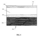
- FIG. 1is an embodiment of the invention that shows a cross-section of the media device 100 in an unwritten state.
- the media device 100includes a substrate 102 , an undercoat 104 , a media 106 and an overcoat 108 .
- Substrate 102supports the media device.
- Undercoat 104can be formed on top of substrate 102 , however, undercoat 104 is not required.
- media 106is formed and then an overcoat 108 is placed after the media 106 .
- Media device 100can be made from a variety of materials.
- media device 100can include an undercoat 104 .
- Undercoat 104can be placed over the substrate.
- the substrateis typically a material with a low conductivity.
- undercoat 104is a highly conductive material.
- one embodimentuses a material for undercoat 104 that includes tungsten.
- Yet another embodiment of undercoat 104includes platinum.
- Other embodiments of undercoat 104can include gold, aluminum, or copper.
- undercoat 104has been described as being a highly conductive material, undercoat 104 can also be an insulator.
- undercoat 104can be made from an oxide or nitride material, thereby insulating the media 106 from the substrate 102 .
- media device 100includes an overcoat 108 .
- Overcoat 108is made from a material that is different from media 106 .
- the overcoat 108is selected to prevent physical damage to the media or to the probe tip when the probe tip comes into contact with overcoat 108 .
- the overcoatis selected to reduce wear of the overcoat and probe tip over an extended time period.
- Overcoat 108typically has a low conductance characteristic, but a high hardness characteristic.
- overcoat 108is made from titanium nitride, which is a poor conductor, but is hard.
- overcoat 108can be made of a diamond-like carbon.
- the conductivity of diamond-like carboncan be adjusted in the manufacturing process through a variety of techniques. One such technique includes using a dopant such as nitrogen in the formation of the diamond-like carbon.
- overcoat 108can be an insulator.
- overcoat 108can be an insulator such as nitride, for example silicon nitride. If an insulator is used for overcoat 108 , then any current applied to memory device 100 will have to tunnel through the insulator before reaching the media 106 . Thus, in one embodiment, the insulator used for overcoat 108 is kept relatively thin, thereby reducing the amount of tunneling required before a current can interact with media 106 . In another embodiment, the insulator for overcoat 108 is an oxide. A number of different insulators are useful for overcoat 108 , and these insulators have an advantage of being very hard.
- media 106is a phase change material.
- media 106is a phase change material such as germanium, tellurium and/or antimony and is commonly known as a chalcogenide.
- a phase change materialis subjected to different temperatures, the phase of the material changes between crystalline and amorphous states.
- the resistivity of the materialchanges. This resistivity change is quite large in phase change materials and can be easily detected by a probe tip that has a conductive coating on it by passing current through the tip and the media.
- Phase change materialsare well known in the art and can be found disclosed in numerous references, for example U.S. Pat. Nos. 3,271,591 and 3,530,441 both issued to Ovshinsky and incorporated herein by reference.
- media 106can be a magneto optic material.
- media device 100can include a lubricant 101 that is placed on top of overcoat 108 .
- lubricant 101can be molybdenum disulfide.
- Lubricant 101can be a liquid.
- Lubricant 101can also be any number of thin liquids.
- Lubricant 101can be applied to overcoat 108 by many different methods. In one embodiment, lubricant 101 is deposited on top of overcoat 108 using a deposition process. In another embodiment, lubricant 101 is sprayed onto overcoat 108 .
- One method of making the media device 100is with a traditional semiconductor manufacturing processes.
- Yet another method of making media device 100is to use a shadow mask.
- a mask wafer that contains at least one apertureis placed over a final wafer, which will contain a memory device 100 .
- the mask wafer and final waferare then subjected to a deposition process. During the deposition process, chemicals pass through the shadow mask and are deposited to form a media device 100 .
- FIG. 2is another embodiment of the invention that shows a cross-section of the media device 200 including data bit.
- Media device 200includes a substrate 202 , an optional undercoat 204 , a media 206 , and an overcoat 208 .
- the media 206further includes a data bit 210 , which represents data stored in the memory device 200 .
- the mediacan be of many different types.
- media device 200includes a charge storage type media 206 .
- Charge storage mediastores data as trapped charges in dielectrics.
- media 206would be a dielectric material that traps charges when media 206 includes a written state. Changing media 206 back to an unwritten state simply requires the removal of the trapped charges. For instance, a positive current can be used to store charges in media 206 . A negative current can then be used to remove the stored charges from media 206 .
- media device 200is a phase change media.
- media 206can include a material that has a resistance characteristic at an ambient state, but the resistance characteristic changes in response to temperature changes. For instance, as a current is applied such that the current passes through media 206 , the temperature of media 206 is increased. After media 206 is heated to a predetermined temperature, the current is removed from media 206 , causing the temperature of media 206 to decrease back to the ambient state of media 206 . During the cooling of media 206 , the resistivity of media 206 changes from its original state, the state before the current was applied. This resistance change is caused by the thermal writing of a crystalline bit.
- media 206When the resistive characteristics of media 206 change from its original state, then media 206 is said to be in a written or crystalline state.
- a second currentis applied to media 206 .
- the second currentcauses media 206 to heat to a second and higher temperature.
- the second currentis then removed from media 206 , causing media 206 to cool back to an ambient temperature.
- the resistivity of media 206returns to the resistivity media 206 had at its original amorphous state, or a close approximation to the original resistivity state of media 206 .
- phase change material for media 206requires media 206 to be heated to a higher temperature for a written state to exist. For instance, applying a first current to media 206 such that media 206 is heated to a temperature approximately equal to 170° C. to 200° C. As media 206 cools back to an ambient state, then the resistivity of media 206 will decrease. To reset media 206 back to an unwritten state, a second current is applied to media 206 causing media 206 to heat to a temperature somewhere in the range of 600° C. As media 206 cools back to an ambient state, any written state to the area of media 206 subjected to the second current and heated to 600° C. will revert back to the resistivity that media 206 possessed before having been changed to a written state.
- Different materialscan be used for media 206 to adjust the operating range for memory writing and resetting the media 206 back to an unwritten state. Altering the proportions of the elements in a chalcogenide is one way of altering the written and erased temperatures.
- media 206begins at an unwritten, ambient state.
- a first currentis applied to media 206 , thereby heating media 206 to a first predetermined temperature.
- a write operationcan require that media 206 be heated to a temperature of at least 170° C.
- the first currentis removed from media 206 and media 206 begins to cool.
- the resistivity of media 206changes such that the new resistivity characteristic can be interpreted as a written state. This state can cause the resistivity of media 206 to increase or decrease, depending on the material used for media 206 .
- a second currentis applied to media 206 .
- Media 206is heated to a second temperature (for instance, media 206 can be heated to a temperature of at least 600° C.).
- the resistivity of media 206is returned back to a state approximately equal to the original state of media 206 , thereby erasing the written data in media 206 .
- the written states within media 206can be also be changed back to the ambient state of media 206 , or an unwritten state, by applying heating to a large region of the memory device 200 .
- memory device 200can apply a current to a buried heater under the memory device 200 . This heating can be applied to all of the memory locations in the memory device 200 such that the resistivity characteristics of media 206 is returned to the ambient state throughout the entire memory device 200 .
- the ambient, or unwritten, state of memory device 200has the media 206 having a high resistivity, and the written state of media 206 having a low resistivity. In other embodiments these states can be reversed such that the ambient, or unwritten state, for memory device 200 has media 206 having a low resistivity and a written state has media 206 having a high resistivity.
- Another embodiment of memory device 200can have media 206 capable of having a plurality of resistivity states.
- the media 206 of memory device 200can have a first resistivity.
- Media 206can then be heated to different temperatures and then cooled, thereby changing the resistivity of media 206 .
- One embodimentsenses whether the resistivity for media 206 is at or near the ambient state for media 206 or at some state that is sufficiently different to be measured as a state different than ambient, or unwritten.
- Another embodimentis able to sense a plurality of resistivity states that media 206 can possess.
- media 206begins with some first resistivity characteristic at an ambient, or unwritten state.
- a first currentis then applied to media 206 , thereby heating media 206 to a first temperature.
- the first currentis then removed from media 206 , which thereby begins to cool.
- media 206gains a second resistivity characteristic.
- the second resistivity characteristic of media 206can be measured more precisely than simply whether the second resistivity characteristic is different from the first resistivity characteristic.
- the second resistivity characteristiccan vary depending on the temperature that the media 206 is heated to by the first current.
- the different resistivity characteristics that can be represented by the second resistivity characteristiccan be representative of a range of data values. This range of data values can be classified in discrete ranges to represent analog values.
- the precise value of the resistivity characteristic for media 206can be measured for more precise analog data storage. Measurements of the resistivity are preferentially obtained by taking measurements which are relative to a first state of the media, but can also be obtained by taking absolute value measurements. Another method of measurement extracts the data as the derivative of the measured data.
- Media 206can posses a large dynamic range for resistivity states, thereby allowing analog data storage.
- the dynamic range for the resistivity characteristic of media 206can be approximately 1000-10,000 (or 10 ⁇ 3 to 10 ⁇ 4) orders of magnitude. In one embodiment, however, heating from the probe on the phase change material can cause only a very small area of media 206 to undergo a change in its resistivity. In this form a smaller dynamic range maybe observed, as only a small region of the media is altered.
- FIG. 3is another embodiment of the invention that shows a cross-section of the media device 300 including a data bit where an embodiment of an atomic probe 311 is in contact with the media device 300 .
- Atomic probe 311includes a core 310 and a coating 312 .
- Media device 300includes a substrate 302 connected with undercoat 304 .
- Undercoat 304 of memory device 300is connected with media 306 .
- Media 306includes a data bit 314 .
- Media 306 and data bit 314are connected with overcoat 308 .
- Atomic probe 311is in contact with overcoat 308 .
- Memory device 300can be any one of the embodiments described above in FIGS. 1 and 2 .
- atomic probe 311includes core 310 and coating 312 with a generally conical shape.
- atomic probe 311has a generally conical shape, however, atomic probe 311 can also be described as having a generally trapezoidal shape.
- Atomic probe 311can have a radius of curvature 313 from a few nanometers to as much as fifty nanometers or more. The radius of curvature 313 is measured from a line 309 generally extending down the center of the atomic probe 311 .
- Atomic probe 311is generally symmetrical along the line 309 , but as will be seen below, atomic probe 311 is not limited to being symmetrical along the line 309 .
- the atomic probe 311should make contact with the memory device 300 . This contact can occur where atomic probe 311 contacts the overcoat 308 of the memory device 300 .
- the point of contact on the atomic probe 311is generally conductive.
- the atomic probe 311includes a core 310 , which is an insulator, that is partially covered by a conductive coating 312 .
- the coating 312 of atomic probe 311makes contact with overcoat 308 of memory device 300 during access of memory device 300 .
- atomic probe 311does not have to make direct contact with overcoat 308 of memory device 300 . Instead, atomic probe 311 is brought in close proximity with memory device 300 such that coating 312 can sense whether a piece of data 314 exists. For instance, if memory device 300 were of a charged storage type memory, then atomic probe 311 would sense the electric and/or magnetic field strength of data 314 through coating 312 .
- the core 310 of atomic probe 311can include oxides, amorphous silicon, or other insulators.
- the coating 312 of atomic probe 311is a conductor and can include any number of different components.
- coating 312can include titanium nitride, platinum, gold, aluminum, tungsten, tungsten carbide, tungsten oxide, diamond-like carbon, platinum iridium, copper, doped silicon or a mixture of such conductors.
- the choice of material for coating 312 of atomic probe 311is influenced by the chosen application for the atomic probe 311 . For instance, some applications require the coating 312 to be an exceptional conductor like platinum, while others do not require such a high conductivity. Titanium nitride can be used for coating 312 and would be beneficial if the application valued a hard coating 312 over a highly conductive coating 312 .
- One embodiment of the inventioncontrols the shape of the coating 312 such that it is rectangular in shape.
- the data 314 formedwill have a generally rectangular shape as opposed to a spherical shape.
- FIG. 4is another embodiment of the invention that shows a cross-section of the media including a data bit where another embodiment of another cantilever tip, or atomic probe 411 , is connected with the media.
- a media device 400is shown that can be any of the memory devices previously discussed.
- Media device 400includes a substrate 402 , an undercoat 404 , a media 406 , and an overcoat 408 .
- Media device 400has been written to and a bit of data 414 formed.
- Atomic probeincludes a core 410 connected with a coating 412 .
- FIG. 4Shown in FIG. 4 , is an embodiment of the invention where the coating 412 of atomic probe 411 is only on one side of atomic probe 411 .
- coating 412provides a path for conducting a current through media device 400 .
- the contact area of coating 412is smaller than the contact area of coating 312 from FIG. 3 .
- the amount of media 406 that can be influenced by a current flowing through coating 412is less than the amount of media 306 that can be influenced by a current flowing through coating 312 from FIG. 3 .
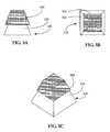
- FIGS. 5A , 5 B, and 5 Cdepict another embodiment of the invention showing another atomic probe 520 with a coating 524 on five sides of a core 522 .
- FIG. 5shows three views of atomic probe 520 .
- FIG. 5Ais a side view of atomic probe 520 where coating 524 is connected with core 522 .
- coating 524covers an entire side of atomic probe 520 .
- FIG. 5Bis a top view of atomic probe 520 .
- FIG. 5Bshows that the coating 524 protects the core 522 along five surfaces.
- the center square portion of FIG. 5Bis the area that makes contact with a media device.
- One such media devicecan be similar to media device 300 of FIG. 3 .
- FIG. 5Cshows a three dimensional view of atomic probe 520 . As can be seen from FIG. 5C , coating 524 extends away from core 522 .
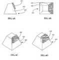
- FIGS. 6A , 6 B, and 6 Cdepict another embodiment of the invention showing another atomic probe 620 with a coating 624 on one side of a core 622 .
- FIG. 6shows three views of atomic probe 620 .
- FIG. 6Ais a side view of atomic probe 620 where coating 624 is connected with core 622 . Coating 624 is only on one side of core 622 in FIG. 6 . Also, coating 624 extends past the tip 623 of core 622 or can be even with the end of core 622 . Thus, as the atomic probe 620 is brought into contact with a media device, coating 624 will make contact with the media device.
- FIG. 6Bshows a top view of atomic probe 620
- FIG. 6Cshows a three dimensional view of atomic probe 620 with the coating 624 only on one side of core 622 .
- coating 624can be flush with the tip 623 of core 622 similar to the atomic probe 411 shown in FIG. 4 .
- the coating 634 of FIG. 6Ddoes not rest to the side of core 642 , as shown in FIG. 6A , but rather, coating 634 is embedded into core 642 .
- An example of thiswould be applying a preferential doping to one side of a single crystal silicon core, causing the embedded area to be conductive, while the core would remain substantially an insulator.
- FIGS. 7A , 7 B and 7 Cdepict another embodiment of the invention showing another atomic probe 720 with a coating 724 formed on the end of a core 722 .
- coating 724is has a generally button like shape.
- the coating 724 in FIG. 7Chas a generally cylindrical shape.
- FIG. 7Bshows a top view of atomic probe 720 and
- FIG. 7Cshows a three dimensional view of atomic probe 720 .
- coating 724can be any of the materials previously disclosed. In an alternative embodiment, however, coating 724 can include carbon nano-tubes. Carbon nano-tubes are useful because they are very small with known dimensions. Thus, the cross-section of a carbon nano-tube is very small. Furthermore, carbon nano-tubes are very strong, thus they can provide the hardness needed for extended life of an atomic probe. Moreover, the structural make-up of a carbon nano-tube coating is capable of handling temperatures well in excess of 600° C.
- the coating 734 of FIG. 7Ddoes not rest top of core 742 , as shown in FIG. 7 , but rather, coating 734 is embedded into core 742 .
- the coreis conductive, or the core is coated with a conductive coating, such that a conductive path exists between the carbon nanotube and the probe. There also exists a conductive path to the cantilever conductor on which the atomic probe sits.
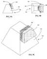
- FIGS. 8A , 8 B, and 8 Cdepict another embodiment of the invention showing another atomic probe 820 with a coating 822 banded on a core 824 .
- FIG. 8Ashows coating 824 draped over the core 822 of atomic probe 820 .
- FIG. 8Bshows how coating 824 is a thin piece of material relative to the dimensions of the core 822 .
- FIG. 8Cis a three dimensional view of atomic probe 820 showing how the coating 824 is draped over core 822 .
- coating 834is also recessed into core 842 .
- the reduced contact area of coating 824 , or coating 834shrinks the affected media, of a media device, when signals are passed through the coating 824 , or the coating 834 , contact is made with a media device by the coating 824 , or the coating 834 .
- less mediais influenced by the atomic probe 820 .
- more datacan be stored in a media device than if a coating 824 , or coating 834 , with a larger contact surface were used.
- FIGS. 9A , 9 B and 9 Cdepict another embodiment of the invention showing another atomic probe 920 with a coating 924 on one side of a core 922 , where coating 924 has a protective material 926 connected with it.
- FIG. 9Ashows a side view of atomic probe 920 .
- Core 922is connected with coating 924 .
- Coating 924is also connected with a protective material 926 .
- FIG. 9Bshows a top view of atomic probe 920 and
- FIG. 9Cshows a three dimensional view of atomic probe 920 .
- atomic probe 920makes contact with a media device, the atomic probe 920 can be dragged or pushed along the media device. Such actions can cause mechanical stresses on the atomic probe 920 , and coating 924 in particular.
- the addition of protective material 926gives additional support to coating 924 , reducing the chance of coating 924 suffering damage due to contact with the media device.
- FIG. 10is a scanning electron microscope view of another embodiment of the invention showing another atomic probe.
- an atomic probe 1020is shown with a tip 1030 .
- the diameter of the base of the atomic probe 1020is less than two micrometers as can be seen by the scale 1032 .
Landscapes
- Engineering & Computer Science (AREA)
- Chemical & Material Sciences (AREA)
- Nanotechnology (AREA)
- Physics & Mathematics (AREA)
- Mathematical Physics (AREA)
- Theoretical Computer Science (AREA)
- Crystallography & Structural Chemistry (AREA)
- Semiconductor Memories (AREA)
Abstract
Description
This application claims priority to the following U.S. Provisional Patent Application:
U.S. Provisional Patent Application No. 60/418,619 entitled “Phase Change Media for High Density Data Storage,” filed Oct. 15, 2002.
U.S. patent application Ser. No. 10/684,883, entitled “Molecular Memory Integrated Circuit Utilizing Non-Vibrating Cantilevers,” filed Oct. 14, 2003;
U.S. patent application Ser. No. 10/684,661, entitled “Atomic Probes and Media for High Density Data Storage,” filed Oct. 14, 2003:
U.S. patent application Ser. No. 10/684,760 entitled “Fault Tolerant Micro-Electro Mechanical Actuators,” filed Oct. 14, 2003;
U.S. Provisional Patent Application No. 60/418,616 entitled “Molecular Memory Integrated Circuit Utilizing Non-Vibrating Cantilevers,” filed Oct. 15, 2002;
U.S. Provisional Patent Application No. 60/418,923 entitled “Atomic Probes and Media for High Density Data Storage,” filed Oct. 15, 2002;
U.S. Provisional Patent Application No. 60/418,612 entitled “Fault Tolerant Micro-Electro Mechanical Actuators,” filed Oct. 15, 2002; and
U.S. Provisional Patent Application No. 60/418,618 entitled “Molecular Memory Integrated Circuit,” filed Oct. 15, 2002.
1. Field the Invention
This invention relates to media for high density data storage in molecular memory integrated circuits for use in micro-electric mechanical systems (MEMS).
2. Description of the Related Art
Phase change media are used in the data storage industry as an alternative to traditional recording devices such as magnetic recorders (tape recorders and hard disk drives) and solid state transistors (EEPROM and FLASH). CD-RW data storage discs and recording drives utilize phase change technology to enable write-erase capability on a compact disc-style media format. Like other phase change media technology, CD-RWs take advantage of changes in optical properties when media material is heated above ambient temperature to induce a phase change from a crystalline state to an amorphous state.
Data storage devices using optical phase change media have enabled inexpensive, medium density storage with the flexibility of erase and rewrite capability. Unfortunately, current technology does not enable the very high densities required for use in today's high capacity portable electronics and tomorrow's next generation technology such as systems-on-a-chip and MEMs. Consequently, there is a need for solutions which permit higher density data storage, while still providing the flexibility of current phase change media solutions.
High density data storage requires a media in which to store data. One such media is a phase change media that alters its resistivity when data is written to the media. The media can include an overcoat. The overcoat can help reduce physical damage inflicted on the media from a device such as a cantilever tip in a molecular memory integrated circuit used to write to or read from the media. Additionally, data written to the media can be in many states. Hence, the media can store digital data and/or analog data.
Other objects, aspects and advantages of the invention can be obtained from reviewing the figures, specification and claims.
Further details of the present invention are explained with the help of the attached drawings in which:
Whileundercoat 104 has been described as being a highly conductive material,undercoat 104 can also be an insulator. For instance,undercoat 104 can be made from an oxide or nitride material, thereby insulating themedia 106 from thesubstrate 102.
In another embodiment,media device 100 includes anovercoat 108.Overcoat 108 is made from a material that is different frommedia 106. Theovercoat 108 is selected to prevent physical damage to the media or to the probe tip when the probe tip comes into contact withovercoat 108. The overcoat is selected to reduce wear of the overcoat and probe tip over an extended time period.Overcoat 108 typically has a low conductance characteristic, but a high hardness characteristic. For instance, in oneembodiment overcoat 108 is made from titanium nitride, which is a poor conductor, but is hard. In another embodiment,overcoat 108 can be made of a diamond-like carbon. The conductivity of diamond-like carbon can be adjusted in the manufacturing process through a variety of techniques. One such technique includes using a dopant such as nitrogen in the formation of the diamond-like carbon.
In yet another embodiment ofmedia device 100,overcoat 108 can be an insulator. For instance,overcoat 108 can be an insulator such as nitride, for example silicon nitride. If an insulator is used forovercoat 108, then any current applied tomemory device 100 will have to tunnel through the insulator before reaching themedia 106. Thus, in one embodiment, the insulator used forovercoat 108 is kept relatively thin, thereby reducing the amount of tunneling required before a current can interact withmedia 106. In another embodiment, the insulator forovercoat 108 is an oxide. A number of different insulators are useful forovercoat 108, and these insulators have an advantage of being very hard.
In other embodiments ofmedia device 100,media 106 is a phase change material. In still other embodiments ofmedia device 100,media 106 is a phase change material such as germanium, tellurium and/or antimony and is commonly known as a chalcogenide. As a phase change material is subjected to different temperatures, the phase of the material changes between crystalline and amorphous states. As a result of this phase change, the resistivity of the material changes. This resistivity change is quite large in phase change materials and can be easily detected by a probe tip that has a conductive coating on it by passing current through the tip and the media. Phase change materials are well known in the art and can be found disclosed in numerous references, for example U.S. Pat. Nos. 3,271,591 and 3,530,441 both issued to Ovshinsky and incorporated herein by reference.
In yet another embodiment ofmedia device 100,media 106 can be a magneto optic material.
In addition toovercoat 108,media device 100 can include alubricant 101 that is placed on top ofovercoat 108. For instance, in one embodiment,lubricant 101 can be molybdenum disulfide.Lubricant 101 can be a liquid.Lubricant 101 can also be any number of thin liquids.Lubricant 101 can be applied toovercoat 108 by many different methods. In one embodiment,lubricant 101 is deposited on top ofovercoat 108 using a deposition process. In another embodiment,lubricant 101 is sprayed ontoovercoat 108.
One method of making themedia device 100 is with a traditional semiconductor manufacturing processes. Yet another method of makingmedia device 100 is to use a shadow mask. Thus, a mask wafer that contains at least one aperture is placed over a final wafer, which will contain amemory device 100. The mask wafer and final wafer are then subjected to a deposition process. During the deposition process, chemicals pass through the shadow mask and are deposited to form amedia device 100.
The media can be of many different types. One embodiment is wheremedia device 200 includes a chargestorage type media 206. Charge storage media stores data as trapped charges in dielectrics. Thus, for charge storage media,media 206 would be a dielectric material that traps charges whenmedia 206 includes a written state. Changingmedia 206 back to an unwritten state simply requires the removal of the trapped charges. For instance, a positive current can be used to store charges inmedia 206. A negative current can then be used to remove the stored charges frommedia 206.
Another embodiment is wheremedia device 200 is a phase change media. Thus,media 206 can include a material that has a resistance characteristic at an ambient state, but the resistance characteristic changes in response to temperature changes. For instance, as a current is applied such that the current passes throughmedia 206, the temperature ofmedia 206 is increased. Aftermedia 206 is heated to a predetermined temperature, the current is removed frommedia 206, causing the temperature ofmedia 206 to decrease back to the ambient state ofmedia 206. During the cooling ofmedia 206, the resistivity ofmedia 206 changes from its original state, the state before the current was applied. This resistance change is caused by the thermal writing of a crystalline bit. When the resistive characteristics ofmedia 206 change from its original state, thenmedia 206 is said to be in a written or crystalline state. To erase the written state frommemory 206, a second current is applied tomedia 206. The secondcurrent causes media 206 to heat to a second and higher temperature. The second current is then removed frommedia 206, causingmedia 206 to cool back to an ambient temperature. Asmedia 206 cools, the resistivity ofmedia 206 returns to theresistivity media 206 had at its original amorphous state, or a close approximation to the original resistivity state ofmedia 206.
Another embodiment of a phase change material formedia 206 requiresmedia 206 to be heated to a higher temperature for a written state to exist. For instance, applying a first current tomedia 206 such thatmedia 206 is heated to a temperature approximately equal to 170° C. to 200° C. Asmedia 206 cools back to an ambient state, then the resistivity ofmedia 206 will decrease. To resetmedia 206 back to an unwritten state, a second current is applied tomedia 206 causingmedia 206 to heat to a temperature somewhere in the range of 600° C. Asmedia 206 cools back to an ambient state, any written state to the area ofmedia 206 subjected to the second current and heated to 600° C. will revert back to the resistivity thatmedia 206 possessed before having been changed to a written state.
Different materials can be used formedia 206 to adjust the operating range for memory writing and resetting themedia 206 back to an unwritten state. Altering the proportions of the elements in a chalcogenide is one way of altering the written and erased temperatures.
Yet another embodiment of themedia device 200 has the resistivity ofmedia 206 changed in a similar way, except thatmedia 206 is also self-quenching. Thus,media 206 begins at an unwritten, ambient state. A first current is applied tomedia 206, therebyheating media 206 to a first predetermined temperature. For instance, a write operation can require thatmedia 206 be heated to a temperature of at least 170° C. Then, the first current is removed frommedia 206 andmedia 206 begins to cool. Asmedia 206 cools, the resistivity ofmedia 206 changes such that the new resistivity characteristic can be interpreted as a written state. This state can cause the resistivity ofmedia 206 to increase or decrease, depending on the material used formedia 206. Subsequently, to erase the written memory tomedia 206, a second current is applied tomedia 206.Media 206 is heated to a second temperature (for instance,media 206 can be heated to a temperature of at least 600° C.). Asmedia 206 cools, the resistivity ofmedia 206 is returned back to a state approximately equal to the original state ofmedia 206, thereby erasing the written data inmedia 206.
The written states withinmedia 206, however, can be also be changed back to the ambient state ofmedia 206, or an unwritten state, by applying heating to a large region of thememory device 200. For instance,memory device 200 can apply a current to a buried heater under thememory device 200. This heating can be applied to all of the memory locations in thememory device 200 such that the resistivity characteristics ofmedia 206 is returned to the ambient state throughout theentire memory device 200.
As described above in some of the various embodiments ofmedia device 200, the ambient, or unwritten, state ofmemory device 200 has themedia 206 having a high resistivity, and the written state ofmedia 206 having a low resistivity. In other embodiments these states can be reversed such that the ambient, or unwritten state, formemory device 200 hasmedia 206 having a low resistivity and a written state hasmedia 206 having a high resistivity.
Another embodiment ofmemory device 200 can havemedia 206 capable of having a plurality of resistivity states. For example, at the ambient state, themedia 206 ofmemory device 200 can have a first resistivity.Media 206 can then be heated to different temperatures and then cooled, thereby changing the resistivity ofmedia 206. One embodiment senses whether the resistivity formedia 206 is at or near the ambient state formedia 206 or at some state that is sufficiently different to be measured as a state different than ambient, or unwritten. Another embodiment is able to sense a plurality of resistivity states thatmedia 206 can possess.
For instance,media 206 begins with some first resistivity characteristic at an ambient, or unwritten state. A first current is then applied tomedia 206, therebyheating media 206 to a first temperature. The first current is then removed frommedia 206, which thereby begins to cool. Asmedia 206 cools,media 206 gains a second resistivity characteristic. In one embodiment, the second resistivity characteristic ofmedia 206 can be measured more precisely than simply whether the second resistivity characteristic is different from the first resistivity characteristic. The second resistivity characteristic can vary depending on the temperature that themedia 206 is heated to by the first current. Thus, the different resistivity characteristics that can be represented by the second resistivity characteristic can be representative of a range of data values. This range of data values can be classified in discrete ranges to represent analog values. Alternatively, the precise value of the resistivity characteristic formedia 206 can be measured for more precise analog data storage. Measurements of the resistivity are preferentially obtained by taking measurements which are relative to a first state of the media, but can also be obtained by taking absolute value measurements. Another method of measurement extracts the data as the derivative of the measured data.
One embodiment of theatomic probe 311 includescore 310 andcoating 312 with a generally conical shape. For instance,atomic probe 311 has a generally conical shape, however,atomic probe 311 can also be described as having a generally trapezoidal shape.Atomic probe 311 can have a radius ofcurvature 313 from a few nanometers to as much as fifty nanometers or more. The radius ofcurvature 313 is measured from aline 309 generally extending down the center of theatomic probe 311.Atomic probe 311 is generally symmetrical along theline 309, but as will be seen below,atomic probe 311 is not limited to being symmetrical along theline 309.
In one embodiment, either to write adata bit 314 or read adata bit 314 to thememory device 300, theatomic probe 311 should make contact with thememory device 300. This contact can occur whereatomic probe 311 contacts theovercoat 308 of thememory device 300. The point of contact on theatomic probe 311 is generally conductive. Thus, in one embodiment, theatomic probe 311 includes acore 310, which is an insulator, that is partially covered by aconductive coating 312. Thecoating 312 ofatomic probe 311 makes contact withovercoat 308 ofmemory device 300 during access ofmemory device 300.
In another embodiment of the invention, during a read operation,atomic probe 311 does not have to make direct contact withovercoat 308 ofmemory device 300. Instead,atomic probe 311 is brought in close proximity withmemory device 300 such thatcoating 312 can sense whether a piece ofdata 314 exists. For instance, ifmemory device 300 were of a charged storage type memory, thenatomic probe 311 would sense the electric and/or magnetic field strength ofdata 314 throughcoating 312.
In one embodiment, thecore 310 ofatomic probe 311 can include oxides, amorphous silicon, or other insulators. Thecoating 312 ofatomic probe 311 is a conductor and can include any number of different components. For instance, coating312 can include titanium nitride, platinum, gold, aluminum, tungsten, tungsten carbide, tungsten oxide, diamond-like carbon, platinum iridium, copper, doped silicon or a mixture of such conductors. The choice of material for coating312 ofatomic probe 311 is influenced by the chosen application for theatomic probe 311. For instance, some applications require thecoating 312 to be an exceptional conductor like platinum, while others do not require such a high conductivity. Titanium nitride can be used for coating312 and would be beneficial if the application valued ahard coating 312 over a highlyconductive coating 312.
One embodiment of the invention controls the shape of thecoating 312 such that it is rectangular in shape. Thus, during a write function to thememory device 300, thedata 314 formed will have a generally rectangular shape as opposed to a spherical shape.
Shown inFIG. 4 , is an embodiment of the invention where thecoating 412 ofatomic probe 411 is only on one side ofatomic probe 411. Thus, whenatomic probe 411 makes contact withmedia device 400, a smaller portion ofatomic probe 411 can potentially affectmedia device 400. For instance, during a write operation by theatomic probe 411 wheremedia 400 is a phase change media, coating412 provides a path for conducting a current throughmedia device 400. The contact area ofcoating 412 is smaller than the contact area of coating312 from FIG.3. Thus, the amount ofmedia 406 that can be influenced by a current flowing throughcoating 412 is less than the amount ofmedia 306 that can be influenced by a current flowing throughcoating 312 from FIG.3.
In an alternative embodiment, coating624 can be flush with the tip623 ofcore 622 similar to theatomic probe 411 shown in FIG.4.
In another embodiment of the invention, the coating634 ofFIG. 6D does not rest to the side of core642, as shown inFIG. 6A , but rather, coating634 is embedded into core642. An example of this would be applying a preferential doping to one side of a single crystal silicon core, causing the embedded area to be conductive, while the core would remain substantially an insulator.
The material used for coating724 can be any of the materials previously disclosed. In an alternative embodiment, however, coating724 can include carbon nano-tubes. Carbon nano-tubes are useful because they are very small with known dimensions. Thus, the cross-section of a carbon nano-tube is very small. Furthermore, carbon nano-tubes are very strong, thus they can provide the hardness needed for extended life of an atomic probe. Moreover, the structural make-up of a carbon nano-tube coating is capable of handling temperatures well in excess of 600° C.
In another embodiment of the invention, the coating734 ofFIG. 7D does not rest top of core742, as shown inFIG. 7 , but rather, coating734 is embedded into core742.
In these embodiments the core is conductive, or the core is coated with a conductive coating, such that a conductive path exists between the carbon nanotube and the probe. There also exists a conductive path to the cantilever conductor on which the atomic probe sits.
Asatomic probe 920 makes contact with a media device, theatomic probe 920 can be dragged or pushed along the media device. Such actions can cause mechanical stresses on theatomic probe 920, andcoating 924 in particular. The addition ofprotective material 926 gives additional support tocoating 924, reducing the chance of coating924 suffering damage due to contact with the media device.
The foregoing description of the present invention have been presented for purposes of illustration and description. It is not intended to be exhaustive or to limit the invention to the precise forms disclosed. Many modifications and variations will be apparent to practitioners skilled in this art. The embodiments were chosen and described in order to best explain the principles of the invention and its practical application, thereby enabling others skilled in the art to understand the invention for various embodiments and with various modifications as are suited to the particular use contemplated. It is intended that the scope of the invention be defined by the following claims and their equivalents.
Claims (24)
1. A media device for high density data storage, comprising:
a media;
an overcoat connected with the media, the overcoat comprising a conductor; and
wherein data is written-to, erased from, or rewritten to the media through the overcoat by an atomic probe tip.
2. The media device ofclaim 1 , wherein data is read from the media by the atomic probe tip.
3. The media device ofclaim 2 , wherein the media is a phase change media.
4. The media device ofclaim 2 , including a lubricant coupled with the overcoat.
5. The media device ofclaim 4 , wherein the undercoat is an insulator.
6. The media device ofclaim 5 , wherein the undercoat is comprised of one of nitride and oxide.
7. The media device ofclaim 2 , including an undercoat coupled with the media.
8. The media device ofclaim 2 , including a substrate coupled with the media.
9. The media device ofclaim 2 , wherein the overcoat has a hardness that is greater than a hardness of the media.
10. The media device ofclaim 2 , wherein the overcoat is softer than the atomic probe tip.
11. The media device ofclaim 10 , wherein the overcoat is comprised of carbon.
12. The media device ofclaim 11 , wherein the overcoat is doped with nitrogen.
13. The media device ofclaim 10 , wherein the overcoat is comprised of titanium nitride.
14. The media device ofclaim 4 , wherein the undercoat is a conductor.
15. The media device ofclaim 14 , wherein the undercoat is comprised of one or more of tungsten, platinum, gold, aluminum and copper.
16. The media device ofclaim 2 , wherein when a positive current is applied by the atomic probe tip to the media, a charge is stored on the media.
17. The media device ofclaim 16 , wherein when a negative current is applied by the atomic probe tip to the media, the charge is released from the media.
18. The media device ofclaim 2 , wherein when a temperature of a portion of the media is increased from an ambient temperature to a first temperature by interaction of the atomic probe tip with the portion and subsequently decreased to the ambient temperature by removing interaction of the atomic probe tip with the portion, the resistivity of the portion changes from a first resistivity to a second resistivity.
19. The media device ofclaim 18 , wherein when a temperature of the portion is increased from the ambient temperature to a third temperature by interaction of the atomic probe tip with the portion and subsequently decreased to the ambient temperature by removing interaction of the probe tip with the portion, the resistivity of the portion changes from the second resistivity to approximately the first resistivity.
20. A media device for high density data storage, comprising:
a substrate;
a media coupled with the substrate;
an overcoat coupled with the media, the overcoat comprising a conductor;
wherein data is written to, erased from, or rewritten to the media through the overcoat by an atomic probe tip.
21. The media device ofclaim 20 , wherein data is read from the media by the atomic probe.
22. The media device ofclaim 21 , wherein the hardness of the overcoat is greater than the hardness of the media.
23. The media device ofclaim 21 , wherein the hardness of the overcoat is less than the hardness of the atomic probe tip.
24. The media device ofclaim 20 , including a lubricant.
Priority Applications (6)
| Application Number | Priority Date | Filing Date | Title |
|---|---|---|---|
| US10/685,045US6985377B2 (en) | 2002-10-15 | 2003-10-14 | Phase change media for high density data storage |
| JP2004545368AJP2006516171A (en) | 2002-10-15 | 2003-10-15 | Atomic probes and media for high density data storage |
| KR1020057006388AKR20050083759A (en) | 2002-10-15 | 2003-10-15 | Phase change media for high density data storage |
| EP03777626AEP1576588A4 (en) | 2002-10-15 | 2003-10-15 | Phase change media for high density data storage |
| PCT/US2003/032793WO2004036554A2 (en) | 2002-10-15 | 2003-10-15 | Phase change media for high density data storage |
| AU2003287102AAU2003287102A1 (en) | 2002-10-15 | 2003-10-15 | Phase change media for high density data storage |
Applications Claiming Priority (2)
| Application Number | Priority Date | Filing Date | Title |
|---|---|---|---|
| US41861902P | 2002-10-15 | 2002-10-15 | |
| US10/685,045US6985377B2 (en) | 2002-10-15 | 2003-10-14 | Phase change media for high density data storage |
Publications (2)
| Publication Number | Publication Date |
|---|---|
| US20040145941A1 US20040145941A1 (en) | 2004-07-29 |
| US6985377B2true US6985377B2 (en) | 2006-01-10 |
Family
ID=32110174
Family Applications (1)
| Application Number | Title | Priority Date | Filing Date |
|---|---|---|---|
| US10/685,045Expired - Fee RelatedUS6985377B2 (en) | 2002-10-15 | 2003-10-14 | Phase change media for high density data storage |
Country Status (6)
| Country | Link |
|---|---|
| US (1) | US6985377B2 (en) |
| EP (1) | EP1576588A4 (en) |
| JP (1) | JP2006516171A (en) |
| KR (1) | KR20050083759A (en) |
| AU (1) | AU2003287102A1 (en) |
| WO (1) | WO2004036554A2 (en) |
Cited By (26)
| Publication number | Priority date | Publication date | Assignee | Title |
|---|---|---|---|---|
| US20020138301A1 (en)* | 2001-03-22 | 2002-09-26 | Thanos Karras | Integration of a portal into an application service provider data archive and/or web based viewer |
| US20050243660A1 (en)* | 2004-04-16 | 2005-11-03 | Rust Thomas F | Methods for erasing bit cells in a high density data storage device |
| US20050243592A1 (en)* | 2004-04-16 | 2005-11-03 | Rust Thomas F | High density data storage device having eraseable bit cells |
| US20060011902A1 (en)* | 2004-07-19 | 2006-01-19 | Samsung Electronics Co., Ltd. | Phase change memory device and method for forming the same |
| US20060120140A1 (en)* | 2002-10-15 | 2006-06-08 | Nanochip, Inc. | Atomic probes and media for high density data storage |
| US20060291271A1 (en)* | 2005-06-24 | 2006-12-28 | Nanochip, Inc. | High density data storage devices having servo indicia formed in a patterned media |
| US20070010054A1 (en)* | 2005-07-08 | 2007-01-11 | Nanochip, Inc. | Method for forming patterned media for a high density data storage device |
| US20070008866A1 (en)* | 2005-07-08 | 2007-01-11 | Nanochip, Inc. | Methods for writing and reading in a polarity-dependent memory switch media |
| US20070006455A1 (en)* | 2005-06-24 | 2007-01-11 | Nanochip, Inc. | Methods for forming high density data storage devices with read/write probes with hollow or reinforced tips |
| US20070008865A1 (en)* | 2005-07-08 | 2007-01-11 | Nanochip, Inc. | High density data storage devices with polarity-dependent memory switching media |
| US20070008864A1 (en)* | 2005-06-24 | 2007-01-11 | Nanochip, Inc. | Patterned media for a high density data storage device |
| US20070008867A1 (en)* | 2005-07-08 | 2007-01-11 | Nanochip, Inc. | High density data storage devices with a lubricant layer comprised of a field of polymer chains |
| US20070165444A1 (en)* | 1998-12-18 | 2007-07-19 | Nanochip, Inc. | Devices and methods of detecting movement between media and probe tip in a probe data storage system |
| US20080001075A1 (en)* | 2006-06-15 | 2008-01-03 | Nanochip, Inc. | Memory stage for a probe storage device |
| US20080042167A1 (en)* | 2006-08-16 | 2008-02-21 | Yi-Chou Chen | Phase change materials and associated memory devices |
| US20080175033A1 (en)* | 2007-01-19 | 2008-07-24 | Nanochip, Inc. | Method and system for improving domain stability in a ferroelectric media |
| US20080174918A1 (en)* | 2007-01-19 | 2008-07-24 | Nanochip, Inc. | Method and system for writing and reading a charge-trap media with a probe tip |
| US20080233672A1 (en)* | 2007-03-20 | 2008-09-25 | Nanochip, Inc. | Method of integrating mems structures and cmos structures using oxide fusion bonding |
| US20090113739A1 (en)* | 2007-11-01 | 2009-05-07 | International Business Machines Corporation | Dual carbon nanotubes for critical dimension metrology on high aspect ratio semiconductor wafer patterns |
| US20090129246A1 (en)* | 2007-11-21 | 2009-05-21 | Nanochip, Inc. | Environmental management of a probe storage device |
| US20090294028A1 (en)* | 2008-06-03 | 2009-12-03 | Nanochip, Inc. | Process for fabricating high density storage device with high-temperature media |
| US20090305508A1 (en)* | 2003-12-10 | 2009-12-10 | International Business Machines Corporation | Integrated circuit with upstanding stylus |
| US20100039919A1 (en)* | 2008-08-15 | 2010-02-18 | Nanochip, Inc. | Cantilever Structure for Use in Seek-and-Scan Probe Storage |
| US20100039729A1 (en)* | 2008-08-14 | 2010-02-18 | Nanochip, Inc. | Package with integrated magnets for electromagnetically-actuated probe-storage device |
| US20100295560A1 (en)* | 2008-09-30 | 2010-11-25 | Quan Tran | Scanning Impedance Microscopy (SIM) To Map Local Impedance In A Dielectric Film |
| US8987701B2 (en) | 2009-05-28 | 2015-03-24 | Cornell University | Phase transition memories and transistors |
Families Citing this family (9)
| Publication number | Priority date | Publication date | Assignee | Title |
|---|---|---|---|---|
| US7471552B2 (en)* | 2003-08-04 | 2008-12-30 | Ovonyx, Inc. | Analog phase change memory |
| FR2870037B1 (en)* | 2004-05-04 | 2006-07-14 | Commissariat Energie Atomique | INFORMATION RECORDING SYSTEM AND METHOD OF USING SUCH A SYSTEM |
| CN100397676C (en)* | 2004-08-06 | 2008-06-25 | 中国科学院上海微系统与信息技术研究所 | Characterization method of electrical properties of reversible phase change materials |
| WO2007002370A2 (en)* | 2005-06-24 | 2007-01-04 | Nanochip, Inc. | Media for writing highly resolved domains |
| US8525143B2 (en)* | 2005-09-06 | 2013-09-03 | Nantero Inc. | Method and system of using nanotube fabrics as joule heating elements for memories and other applications |
| US7940628B2 (en) | 2005-12-02 | 2011-05-10 | Ricoh Company, Ltd. | Multilayer optical information recording medium, optical head, and optical drive |
| FR2901400B1 (en)* | 2006-05-18 | 2008-12-26 | Commissariat Energie Atomique | EFFECT DATA RECORDING MEDIUM HAVING LOCALIZED ELECTRIC CONDUCTION LAYER |
| US10368146B2 (en)* | 2016-09-20 | 2019-07-30 | General Electric Company | Systems and methods for environment sensing |
| US7859036B2 (en) | 2007-04-05 | 2010-12-28 | Micron Technology, Inc. | Memory devices having electrodes comprising nanowires, systems including same and methods of forming same |
Citations (158)
| Publication number | Priority date | Publication date | Assignee | Title |
|---|---|---|---|---|
| US4340953A (en) | 1979-05-14 | 1982-07-20 | Nippon Hoso Kyokai | Information recording medium and recording and reproducing system using the same |
| US4575822A (en) | 1983-02-15 | 1986-03-11 | The Board Of Trustees Of The Leland Stanford Junior University | Method and means for data storage using tunnel current data readout |
| US4710899A (en) | 1985-06-10 | 1987-12-01 | Energy Conversion Devices, Inc. | Data storage medium incorporating a transition metal for increased switching speed |
| US4719594A (en) | 1984-11-01 | 1988-01-12 | Energy Conversion Devices, Inc. | Grooved optical data storage device including a chalcogenide memory layer |
| US4737934A (en) | 1985-10-18 | 1988-04-12 | Energy Conversion Devices, Inc. | Data storage device and system having an optically non transmissive chalcogenide layer |
| US4744055A (en) | 1985-07-08 | 1988-05-10 | Energy Conversion Devices, Inc. | Erasure means and data storage system incorporating improved erasure means |
| US4769338A (en) | 1984-05-14 | 1988-09-06 | Energy Conversion Devices, Inc. | Thin film field effect transistor and method of making same |
| US4769682A (en) | 1984-11-05 | 1988-09-06 | Energy Conversion Devices, Inc. | Boron doped semiconductor materials and method for producing same |
| US4775425A (en) | 1987-07-27 | 1988-10-04 | Energy Conversion Devices, Inc. | P and n-type microcrystalline semiconductor alloy material including band gap widening elements, devices utilizing same |
| US4792501A (en) | 1985-05-15 | 1988-12-20 | Energy Conversion Devices, Inc. | Multilayered article including crystallization inhibiting layer and method for fabricating same |
| US4820394A (en) | 1984-11-21 | 1989-04-11 | Energy Conversion Devices, Inc. | Phase changeable material |
| US4829507A (en) | 1984-09-14 | 1989-05-09 | Xerox Corporation | Method of and system for atomic scale readout of recorded information |
| US4831614A (en) | 1986-05-27 | 1989-05-16 | International Business Machines Corporation | Direct access storage unit using tunneling current techniques |
| US4843443A (en) | 1984-05-14 | 1989-06-27 | Energy Conversion Devices, Inc. | Thin film field effect transistor and method of making same |
| US4845533A (en) | 1986-08-22 | 1989-07-04 | Energy Conversion Devices, Inc. | Thin film electrical devices with amorphous carbon electrodes and method of making same |
| US4868616A (en) | 1986-12-11 | 1989-09-19 | Energy Conversion Devices, Inc. | Amorphous electronic matrix array for liquid crystal display |
| US4876667A (en) | 1987-06-22 | 1989-10-24 | Energy Conversion Devices, Inc. | Data storage device having a phase change memory medium reversible by direct overwrite |
| US4882295A (en) | 1985-07-26 | 1989-11-21 | Energy Conversion Devices, Inc. | Method of making a double injection field effect transistor |
| US4883686A (en) | 1988-05-26 | 1989-11-28 | Energy Conversion Devices, Inc. | Method for the high rate plasma deposition of high quality material |
| US4891330A (en) | 1987-07-27 | 1990-01-02 | Energy Conversion Devices, Inc. | Method of fabricating n-type and p-type microcrystalline semiconductor alloy material including band gap widening elements |
| US4916688A (en) | 1988-03-31 | 1990-04-10 | International Business Machines Corporation | Data storage method using state transformable materials |
| US4924436A (en) | 1987-06-22 | 1990-05-08 | Energy Conversion Devices, Inc. | Data storage device having a phase change memory medium reversible by direct overwrite and method of direct overwrite |
| US4945515A (en) | 1987-09-10 | 1990-07-31 | Seiko Instruments, Inc. | Memory writing apparatus |
| US4962480A (en) | 1987-09-10 | 1990-10-09 | Seiko Instruments, Inc. | Memory reading apparatus |
| US4987312A (en) | 1989-11-07 | 1991-01-22 | International Business Machines Corporation | Process for repositioning atoms on a surface using a scanning tunneling microscope |
| US5008617A (en) | 1989-06-20 | 1991-04-16 | Energy Conversion Devices, Inc. | Functional testing of ultra large area, ultra large scale integrated circuits |
| US5038322A (en) | 1988-09-21 | 1991-08-06 | U.S. Philips Corporation | Method of and device for sub-micron processing a surface |
| US5043578A (en) | 1990-04-05 | 1991-08-27 | International Business Machines Corporation | Writing atomic scale features with fine tip as source of deposited atoms |
| US5051977A (en) | 1989-08-30 | 1991-09-24 | Hoechst Celanese Corp. | Scanning tunneling microscope memory utilizing optical fluorescence of substrate for reading |
| US5091880A (en) | 1989-02-02 | 1992-02-25 | Olympus Optical Co., Ltd. | Memory device |
| US5095479A (en) | 1990-08-13 | 1992-03-10 | Ricoh Company, Ltd. | Optical information recording medium |
| US5097443A (en) | 1989-03-28 | 1992-03-17 | Canon Kabushiki Kaisha | Storage medium, storage method and stored information reading method |
| US5103284A (en) | 1991-02-08 | 1992-04-07 | Energy Conversion Devices, Inc. | Semiconductor with ordered clusters |
| US5126635A (en) | 1988-04-08 | 1992-06-30 | Energy Conversion Devices, Inc. | Microwave plasma operation using a high power microwave transmissive window assembly |
| US5128099A (en) | 1991-02-15 | 1992-07-07 | Energy Conversion Devices, Inc. | Congruent state changeable optical memory material and device |
| US5144581A (en)* | 1989-02-09 | 1992-09-01 | Olympus Optical Co., Ltd. | Apparatus including atomic probes utilizing tunnel current to read, write and erase data |
| US5144148A (en) | 1989-11-07 | 1992-09-01 | International Business Machines Corporation | Process for repositioning atoms on a surface using a scanning tunneling microscope |
| US5159661A (en) | 1990-10-05 | 1992-10-27 | Energy Conversion Devices, Inc. | Vertically interconnected parallel distributed processor |
| US5166758A (en) | 1991-01-18 | 1992-11-24 | Energy Conversion Devices, Inc. | Electrically erasable phase change memory |
| US5177567A (en) | 1991-07-19 | 1993-01-05 | Energy Conversion Devices, Inc. | Thin-film structure for chalcogenide electrical switching devices and process therefor |
| US5180690A (en) | 1988-12-14 | 1993-01-19 | Energy Conversion Devices, Inc. | Method of forming a layer of doped crystalline semiconductor alloy material |
| US5180686A (en) | 1988-10-31 | 1993-01-19 | Energy Conversion Devices, Inc. | Method for continuously deposting a transparent oxide material by chemical pyrolysis |
| US5187367A (en) | 1990-08-14 | 1993-02-16 | Canon Kabushiki Kaisha | Cantilever type probe, scanning tunneling microscope and information processing device equipped with said probe |
| US5196701A (en) | 1991-07-31 | 1993-03-23 | International Business Machines Corporation | High-resolution detection of material property variations |
| US5216631A (en) | 1990-11-02 | 1993-06-01 | Sliwa Jr John W | Microvibratory memory device |
| US5223308A (en) | 1991-10-18 | 1993-06-29 | Energy Conversion Devices, Inc. | Low temperature plasma enhanced CVD process within tubular members |
| US5231047A (en) | 1991-12-19 | 1993-07-27 | Energy Conversion Devices, Inc. | High quality photovoltaic semiconductor material and laser ablation method of fabrication same |
| US5251200A (en) | 1990-09-14 | 1993-10-05 | Canon Kabushiki Kaisha | Tracking method for memory apparatus |
| US5260567A (en) | 1991-04-10 | 1993-11-09 | Canon Kabushiki Kaisha | Cantilever unit and atomic force microscope, magnetic force microscope, reproducing apparatus and information processing apparatus using the cantilever unit |
| US5262981A (en) | 1990-07-03 | 1993-11-16 | Basf Aktiengesellschaft | Storage of information units in the nanometer range |
| US5265046A (en) | 1991-01-07 | 1993-11-23 | Basf Aktiengesellschaft | Chemical labeling of the surfaces of solids on an atomic scale, and the storage of information units in the atomic range |
| US5289455A (en) | 1990-07-25 | 1994-02-22 | Canon Kabushiki Kaisha | Information recording and/or reproducing apparatus |
| US5296716A (en) | 1991-01-18 | 1994-03-22 | Energy Conversion Devices, Inc. | Electrically erasable, directly overwritable, multibit single cell memory elements and arrays fabricated therefrom |
| US5323375A (en) | 1991-03-08 | 1994-06-21 | Hitachi, Ltd. | Information storage apparatus |
| US5324553A (en) | 1993-04-30 | 1994-06-28 | Energy Conversion Devices, Inc. | Method for the improved microwave deposition of thin films |
| US5330630A (en) | 1991-01-02 | 1994-07-19 | Energy Conversion Devices, Inc. | Switch with improved threshold voltage |
| US5341328A (en) | 1991-01-18 | 1994-08-23 | Energy Conversion Devices, Inc. | Electrically erasable memory elements having reduced switching current requirements and increased write/erase cycle life |
| US5359205A (en) | 1991-11-07 | 1994-10-25 | Energy Conversion Devices, Inc. | Electrically erasable memory elements characterized by reduced current and improved thermal stability |
| US5389475A (en) | 1991-06-21 | 1995-02-14 | Canon Kabushiki Kaisha | Recording medium and information-erasing method |
| US5406509A (en) | 1991-01-18 | 1995-04-11 | Energy Conversion Devices, Inc. | Electrically erasable, directly overwritable, multibit single cell memory elements and arrays fabricated therefrom |
| US5412597A (en) | 1990-11-20 | 1995-05-02 | Canon Kabushiki Kaisha | Slope detection method, and information detection/writing apparatus using the method |
| US5411591A (en) | 1992-11-13 | 1995-05-02 | Energy Conversion Devices, Inc. | Apparatus for the simultaneous microwave deposition of thin films in multiple discrete zones |
| US5414271A (en) | 1991-01-18 | 1995-05-09 | Energy Conversion Devices, Inc. | Electrically erasable memory elements having improved set resistance stability |
| US5426092A (en) | 1990-08-20 | 1995-06-20 | Energy Conversion Devices, Inc. | Continuous or semi-continuous laser ablation method for depositing fluorinated superconducting thin film having basal plane alignment of the unit cells deposited on non-lattice-matched substrates |
| US5453970A (en) | 1993-07-13 | 1995-09-26 | Rust; Thomas F. | Molecular memory medium and molecular memory disk drive for storing information using a tunnelling probe |
| US5471458A (en) | 1992-09-10 | 1995-11-28 | Canon Kabushiki Kaisha | Multi-probe information recording/reproducing apparatus including a probe displacement control circuit |
| US5471064A (en) | 1992-09-14 | 1995-11-28 | Hitachi, Ltd. | Precision machining method, precision machining apparatus and data storage apparatus using the same |
| WO1996011472A2 (en) | 1994-10-07 | 1996-04-18 | Hewlett-Packard Company | A memory device |
| US5534711A (en) | 1991-01-18 | 1996-07-09 | Energy Conversion Devices, Inc. | Electrically erasable, directly overwritable, multibit single cell memory elements and arrays fabricated therefrom |
| US5534712A (en) | 1991-01-18 | 1996-07-09 | Energy Conversion Devices, Inc. | Electrically erasable memory elements characterized by reduced current and improved thermal stability |
| US5536947A (en) | 1991-01-18 | 1996-07-16 | Energy Conversion Devices, Inc. | Electrically erasable, directly overwritable, multibit single cell memory element and arrays fabricated therefrom |
| US5537372A (en) | 1991-11-15 | 1996-07-16 | International Business Machines Corporation | High density data storage system with topographic contact sensor |
| US5543737A (en) | 1995-02-10 | 1996-08-06 | Energy Conversion Devices, Inc. | Logical operation circuit employing two-terminal chalcogenide switches |
| US5557596A (en)* | 1995-03-20 | 1996-09-17 | Gibson; Gary | Ultra-high density storage device |
| US5561300A (en) | 1991-12-24 | 1996-10-01 | Hitachi, Ltd. | Atomic switching devices and logical circuits |
| US5562776A (en) | 1994-09-19 | 1996-10-08 | Energy Conversion Devices, Inc. | Apparatus for microwave plasma enhanced physical/chemical vapor deposition |
| US5567241A (en) | 1993-04-30 | 1996-10-22 | Energy Conversion Devices, Inc. | Method and apparatus for the improved microwave deposition of thin films |
| US5591501A (en) | 1995-12-20 | 1997-01-07 | Energy Conversion Devices, Inc. | Optical recording medium having a plurality of discrete phase change data recording points |
| US5596522A (en) | 1991-01-18 | 1997-01-21 | Energy Conversion Devices, Inc. | Homogeneous compositions of microcrystalline semiconductor material, semiconductor devices and directly overwritable memory elements fabricated therefrom, and arrays fabricated from the memory elements |
| US5597411A (en) | 1991-02-19 | 1997-01-28 | Energy Conversion Devices, Inc. | Method of forming a single crystal material |
| WO1997005610A1 (en) | 1995-07-28 | 1997-02-13 | International Business Machines Corporation | Mass-storage applications of local probe arrays |
| US5606162A (en) | 1991-06-13 | 1997-02-25 | British Technology Group Limited | Microprobe for surface-scanning microscopes |
| EP0788149A1 (en) | 1996-02-05 | 1997-08-06 | Hitachi Europe Limited | Method of depositing nanometre scale particles |
| US5670224A (en) | 1992-11-13 | 1997-09-23 | Energy Conversion Devices, Inc. | Modified silicon oxide barrier coatings produced by microwave CVD deposition on polymeric substrates |
| US5679952A (en) | 1994-05-23 | 1997-10-21 | Hitachi, Ltd. | Scanning probe microscope |
| US5687112A (en) | 1996-04-19 | 1997-11-11 | Energy Conversion Devices, Inc. | Multibit single cell memory element having tapered contact |
| US5694054A (en) | 1995-11-28 | 1997-12-02 | Energy Conversion Devices, Inc. | Integrated drivers for flat panel displays employing chalcogenide logic elements |
| US5694146A (en) | 1994-10-14 | 1997-12-02 | Energy Conversion Devices, Inc. | Active matrix LCD array employing thin film chalcogenide threshold switches to isolate individual pixels |
| US5714768A (en) | 1995-10-24 | 1998-02-03 | Energy Conversion Devices, Inc. | Second-layer phase change memory array on top of a logic device |
| US5751685A (en) | 1995-05-30 | 1998-05-12 | Hewlett-Packard Company | Probe for memory device having movable media |
| US5757446A (en) | 1994-10-14 | 1998-05-26 | Energy Conversion Devices, Inc. | Liquid crystal display matrix array employing ovonic threshold switching devices to isolate individual pixels |
| US5778134A (en) | 1992-12-21 | 1998-07-07 | Canon Kabushiki Kaisha | Apparatus for recording and reproducing image information in a recording medium wherein scanning probes are controlled based on editing information |
| US5801472A (en) | 1995-08-18 | 1998-09-01 | Hitchi, Ltd. | Micro-fabricated device with integrated electrostatic actuator |
| US5804710A (en) | 1997-06-05 | 1998-09-08 | International Business Machines Corporation | Atomic force microscope system with multi-directional voice coil actuator for controlling the stylus |
| US5808973A (en) | 1995-09-06 | 1998-09-15 | Kabushiki Kaisha Toshiba | Near field recording and reproducing apparatus |
| US5822285A (en) | 1997-03-31 | 1998-10-13 | International Business Machines Corporation | Atomic force microscopy disk data storage system with nonradial tracking lines |
| US5825046A (en) | 1996-10-28 | 1998-10-20 | Energy Conversion Devices, Inc. | Composite memory material comprising a mixture of phase-change memory material and dielectric material |
| US5835477A (en) | 1996-07-10 | 1998-11-10 | International Business Machines Corporation | Mass-storage applications of local probe arrays |
| US5848077A (en) | 1994-12-31 | 1998-12-08 | Hewlett-Packard Company | Scanning memory device and error correction method |
| US5856967A (en) | 1997-08-27 | 1999-01-05 | International Business Machines Corporation | Atomic force microscopy data storage system with tracking servo from lateral force-sensing cantilever |
| US5912839A (en) | 1998-06-23 | 1999-06-15 | Energy Conversion Devices, Inc. | Universal memory element and method of programming same |
| US5929438A (en) | 1994-08-12 | 1999-07-27 | Nikon Corporation | Cantilever and measuring apparatus using it |
| US5933365A (en) | 1997-06-19 | 1999-08-03 | Energy Conversion Devices, Inc. | Memory element with energy control mechanism |
| US5953306A (en) | 1996-04-25 | 1999-09-14 | Hewlett-Packard Company | Micro needle probe apparatus having probes cantilevered over respective electronic circuits, moving medium memory device including same and method of making same |
| US6001519A (en) | 1997-01-22 | 1999-12-14 | Industrial Technology Research Institute | High molecular weight information recording medium and related data writing method |
| US6028393A (en) | 1998-01-22 | 2000-02-22 | Energy Conversion Devices, Inc. | E-beam/microwave gas jet PECVD method and apparatus for depositing and/or surface modification of thin film materials |
| US6027951A (en) | 1994-01-05 | 2000-02-22 | Macdonald; Noel C. | Method of making high aspect ratio probes with self-aligned control electrodes |
| US6038916A (en) | 1997-07-22 | 2000-03-21 | Digital Instruments | Method and apparatus for measuring energy dissipation by a probe during operation of an atomic force microscope |
| US6075719A (en) | 1999-06-22 | 2000-06-13 | Energy Conversion Devices, Inc. | Method of programming phase-change memory element |
| US6084849A (en) | 1996-05-20 | 2000-07-04 | International Business Machines Corporation | Shape memory alloy recording medium, storage devices based thereon, and method for using these storage devices |
| US6087674A (en) | 1996-10-28 | 2000-07-11 | Energy Conversion Devices, Inc. | Memory element with memory material comprising phase-change material and dielectric material |
| US6087580A (en) | 1996-12-12 | 2000-07-11 | Energy Conversion Devices, Inc. | Semiconductor having large volume fraction of intermediate range order material |
| US6141241A (en) | 1998-06-23 | 2000-10-31 | Energy Conversion Devices, Inc. | Universal memory element with systems employing same and apparatus and method for reading, writing and programming same |
| US6186090B1 (en) | 1999-03-04 | 2001-02-13 | Energy Conversion Devices, Inc. | Apparatus for the simultaneous deposition by physical vapor deposition and chemical vapor deposition and method therefor |
| US6196061B1 (en) | 1998-11-05 | 2001-03-06 | Nanodevices, Inc. | AFM with referenced or differential height measurement |
| US6245280B1 (en) | 1999-06-21 | 2001-06-12 | Energy Conversion Devices, Inc. | Method and apparatus for forming polycrystalline particles |
| US6275410B1 (en) | 2000-11-09 | 2001-08-14 | Hewlett-Packard Co. | Data recording systems and methods for facilitating data recovery with emitter failure |
| US6314014B1 (en) | 1999-12-16 | 2001-11-06 | Ovonyx, Inc. | Programmable resistance memory arrays with reference cells |
| US6339217B1 (en) | 1995-07-28 | 2002-01-15 | General Nanotechnology Llc | Scanning probe microscope assembly and method for making spectrophotometric, near-field, and scanning probe measurements |
| US6366340B1 (en) | 1995-08-18 | 2002-04-02 | Hitachi, Ltd. | Electron exposure apparatus |
| US6369400B2 (en) | 1998-10-30 | 2002-04-09 | International Business Machines Corporation | Magnetic scanning or positioning system with at least two degrees of freedom |
| WO2002037488A1 (en) | 2000-11-03 | 2002-05-10 | International Business Machines Corporation | Afm-based data storage and microscopy |
| JP3295044B2 (en) | 1998-10-23 | 2002-06-24 | ブラザー工業株式会社 | Image data transfer device |
| JP3295043B2 (en) | 1997-10-10 | 2002-06-24 | インダク ゲゼルシャフト フィーア インドゥーストリーベダルフ エム.ベー.ハー. | Method and apparatus for processing flexible bags |
| US20020110074A1 (en) | 2001-02-15 | 2002-08-15 | Gibson Gary A. | Methods for conducting current between a scanned-probe and storage medium |
| US6452891B1 (en) | 2000-01-26 | 2002-09-17 | Energy Conversion Devices, Inc. | Method for initializing a data storage device |
| US20020135917A1 (en) | 2001-03-23 | 2002-09-26 | Davidson Robert J. | Atomic resolution storage systems with enhanced magnetic field protection |
| US6480438B1 (en) | 2001-06-12 | 2002-11-12 | Ovonyx, Inc. | Providing equal cell programming conditions across a large and high density array of phase-change memory cells |
| US6487113B1 (en) | 2001-06-29 | 2002-11-26 | Ovonyx, Inc. | Programming a phase-change memory with slow quench time |
| US20030007443A1 (en) | 2001-07-06 | 2003-01-09 | Nickel Janice H. | Data storage device including nanotube electron sources |
| US6507552B2 (en) | 2000-12-01 | 2003-01-14 | Hewlett-Packard Company | AFM version of diode-and cathodoconductivity-and cathodoluminescence-based data storage media |
| US6511867B2 (en) | 2001-06-30 | 2003-01-28 | Ovonyx, Inc. | Utilizing atomic layer deposition for programmable device |
| US6511862B2 (en) | 2001-06-30 | 2003-01-28 | Ovonyx, Inc. | Modified contact for programmable devices |
| US6522566B2 (en) | 2000-12-01 | 2003-02-18 | Hewlett-Packard Company | System modules with atomic resolution storage memory |
| US6531373B2 (en) | 2000-12-27 | 2003-03-11 | Ovonyx, Inc. | Method of forming a phase-change memory cell using silicon on insulator low electrode in charcogenide elements |
| US6534781B2 (en) | 2000-12-26 | 2003-03-18 | Ovonyx, Inc. | Phase-change memory bipolar array utilizing a single shallow trench isolation for creating an individual active area region for two memory array elements and one bipolar base contact |
| US6542400B2 (en) | 2001-03-27 | 2003-04-01 | Hewlett-Packard Development Company Lp | Molecular memory systems and methods |
| US6545907B1 (en) | 2001-10-30 | 2003-04-08 | Ovonyx, Inc. | Technique and apparatus for performing write operations to a phase change material memory device |
| US20030081532A1 (en) | 2001-10-30 | 2003-05-01 | Gibson Gary A. | Supplementary energy sources for atomic resolution storage memory devices |
| US6563164B2 (en) | 2000-09-29 | 2003-05-13 | Ovonyx, Inc. | Compositionally modified resistive electrode |
| US6566700B2 (en) | 2001-10-11 | 2003-05-20 | Ovonyx, Inc. | Carbon-containing interfacial layer for phase-change memory |
| US6567293B1 (en) | 2000-09-29 | 2003-05-20 | Ovonyx, Inc. | Single level metal memory cell using chalcogenide cladding |
| US6567296B1 (en) | 2001-10-24 | 2003-05-20 | Stmicroelectronics S.R.L. | Memory device |
| US6570784B2 (en) | 2001-06-29 | 2003-05-27 | Ovonyx, Inc. | Programming a phase-change material memory |
| US6589714B2 (en) | 2001-06-26 | 2003-07-08 | Ovonyx, Inc. | Method for making programmable resistance memory element using silylated photoresist |
| US6613604B2 (en) | 2001-08-02 | 2003-09-02 | Ovonyx, Inc. | Method for making small pore for use in programmable resistance memory element |
| US6617192B1 (en) | 1997-10-01 | 2003-09-09 | Ovonyx, Inc. | Electrically programmable memory element with multi-regioned contact |
| US6621095B2 (en) | 2000-09-29 | 2003-09-16 | Ovonyx, Inc. | Method to enhance performance of thermal resistor device |
| US20030185139A1 (en) | 2002-03-28 | 2003-10-02 | Ives Thomas Wayne | High density data storage module |
| US20030189200A1 (en) | 2002-04-04 | 2003-10-09 | Heon Lee | Low heat loss and small contact area composite electrode for a phase change media memory device |
| US6646297B2 (en) | 2000-12-26 | 2003-11-11 | Ovonyx, Inc. | Lower electrode isolation in a double-wide trench |
| US6647766B2 (en) | 1999-12-31 | 2003-11-18 | International Business Machines Corporation | Device for contacting and/or modifying a surface having a cantilever and a method for production of said cantilever |
| US6667900B2 (en) | 2001-12-28 | 2003-12-23 | Ovonyx, Inc. | Method and apparatus to operate a memory cell |
| US6671710B2 (en) | 2002-05-10 | 2003-12-30 | Energy Conversion Devices, Inc. | Methods of computing with digital multistate phase change materials |
| US6673700B2 (en) | 2001-06-30 | 2004-01-06 | Ovonyx, Inc. | Reduced area intersection between electrode and programming element |
| US6696355B2 (en) | 2000-12-14 | 2004-02-24 | Ovonyx, Inc. | Method to selectively increase the top resistance of the lower programming electrode in a phase-change memory |
| US6723421B2 (en) | 2001-10-05 | 2004-04-20 | Energy Conversion Devices, Inc. | Semiconductor with coordinatively irregular structures |
| US6733956B2 (en) | 2001-06-26 | 2004-05-11 | Ovonyx, Inc. | Method for making programmable resistance memory element |
Family Cites Families (11)
| Publication number | Priority date | Publication date | Assignee | Title |
|---|---|---|---|---|
| JPH04114333A (en)* | 1990-09-05 | 1992-04-15 | Canon Inc | Information processor |
| US5141241A (en)* | 1991-10-07 | 1992-08-25 | Freddie Avila | Recreation cart apparatus |
| JPH07105580A (en)* | 1993-10-06 | 1995-04-21 | Hitachi Ltd | Information recording device |
| KR950024146A (en)* | 1994-01-31 | 1995-08-21 | 모리시타 요이찌 | Information recording and reproducing apparatus and information recording and reproducing method |
| US5751683A (en)* | 1995-07-24 | 1998-05-12 | General Nanotechnology, L.L.C. | Nanometer scale data storage device and associated positioning system |
| JPH1040599A (en)* | 1996-07-25 | 1998-02-13 | Tdk Corp | Recording medium and recording reproducing method |
| US5985404A (en)* | 1996-08-28 | 1999-11-16 | Tdk Corporation | Recording medium, method of making, and information processing apparatus |
| DE69721986T2 (en)* | 1997-08-27 | 2004-02-12 | Imec Vzw | Stylus configuration, manufacturing process and use of styluses |
| US6349076B1 (en)* | 1998-06-24 | 2002-02-19 | Seagate Technology Llc | Magneto-optical recording medium having a protective carbon layer |
| US6369340B1 (en)* | 2000-03-10 | 2002-04-09 | General Electric Company | Circuit breaker mechanism for a contact system |
| JP3925610B2 (en)* | 2001-02-13 | 2007-06-06 | 喜萬 中山 | Heat generation probe and heat generation probe device |
- 2003
- 2003-10-14USUS10/685,045patent/US6985377B2/ennot_activeExpired - Fee Related
- 2003-10-15KRKR1020057006388Apatent/KR20050083759A/ennot_activeWithdrawn
- 2003-10-15AUAU2003287102Apatent/AU2003287102A1/ennot_activeAbandoned
- 2003-10-15EPEP03777626Apatent/EP1576588A4/ennot_activeWithdrawn
- 2003-10-15JPJP2004545368Apatent/JP2006516171A/enactivePending
- 2003-10-15WOPCT/US2003/032793patent/WO2004036554A2/enactiveApplication Filing
Patent Citations (166)
| Publication number | Priority date | Publication date | Assignee | Title |
|---|---|---|---|---|
| US4340953A (en) | 1979-05-14 | 1982-07-20 | Nippon Hoso Kyokai | Information recording medium and recording and reproducing system using the same |
| US4575822A (en) | 1983-02-15 | 1986-03-11 | The Board Of Trustees Of The Leland Stanford Junior University | Method and means for data storage using tunnel current data readout |
| US4769338A (en) | 1984-05-14 | 1988-09-06 | Energy Conversion Devices, Inc. | Thin film field effect transistor and method of making same |
| US4843443A (en) | 1984-05-14 | 1989-06-27 | Energy Conversion Devices, Inc. | Thin film field effect transistor and method of making same |
| US4829507A (en) | 1984-09-14 | 1989-05-09 | Xerox Corporation | Method of and system for atomic scale readout of recorded information |
| US4719594A (en) | 1984-11-01 | 1988-01-12 | Energy Conversion Devices, Inc. | Grooved optical data storage device including a chalcogenide memory layer |
| US4769682A (en) | 1984-11-05 | 1988-09-06 | Energy Conversion Devices, Inc. | Boron doped semiconductor materials and method for producing same |
| US4820394A (en) | 1984-11-21 | 1989-04-11 | Energy Conversion Devices, Inc. | Phase changeable material |
| US4792501A (en) | 1985-05-15 | 1988-12-20 | Energy Conversion Devices, Inc. | Multilayered article including crystallization inhibiting layer and method for fabricating same |
| US4710899A (en) | 1985-06-10 | 1987-12-01 | Energy Conversion Devices, Inc. | Data storage medium incorporating a transition metal for increased switching speed |
| US4744055A (en) | 1985-07-08 | 1988-05-10 | Energy Conversion Devices, Inc. | Erasure means and data storage system incorporating improved erasure means |
| US4882295A (en) | 1985-07-26 | 1989-11-21 | Energy Conversion Devices, Inc. | Method of making a double injection field effect transistor |
| US4737934A (en) | 1985-10-18 | 1988-04-12 | Energy Conversion Devices, Inc. | Data storage device and system having an optically non transmissive chalcogenide layer |
| US4831614A (en) | 1986-05-27 | 1989-05-16 | International Business Machines Corporation | Direct access storage unit using tunneling current techniques |
| US4845533A (en) | 1986-08-22 | 1989-07-04 | Energy Conversion Devices, Inc. | Thin film electrical devices with amorphous carbon electrodes and method of making same |
| US4868616A (en) | 1986-12-11 | 1989-09-19 | Energy Conversion Devices, Inc. | Amorphous electronic matrix array for liquid crystal display |
| US4876667A (en) | 1987-06-22 | 1989-10-24 | Energy Conversion Devices, Inc. | Data storage device having a phase change memory medium reversible by direct overwrite |
| US4924436A (en) | 1987-06-22 | 1990-05-08 | Energy Conversion Devices, Inc. | Data storage device having a phase change memory medium reversible by direct overwrite and method of direct overwrite |
| US4775425A (en) | 1987-07-27 | 1988-10-04 | Energy Conversion Devices, Inc. | P and n-type microcrystalline semiconductor alloy material including band gap widening elements, devices utilizing same |
| US4891330A (en) | 1987-07-27 | 1990-01-02 | Energy Conversion Devices, Inc. | Method of fabricating n-type and p-type microcrystalline semiconductor alloy material including band gap widening elements |
| US4945515A (en) | 1987-09-10 | 1990-07-31 | Seiko Instruments, Inc. | Memory writing apparatus |
| US4962480A (en) | 1987-09-10 | 1990-10-09 | Seiko Instruments, Inc. | Memory reading apparatus |
| US4916688A (en) | 1988-03-31 | 1990-04-10 | International Business Machines Corporation | Data storage method using state transformable materials |
| US5126635A (en) | 1988-04-08 | 1992-06-30 | Energy Conversion Devices, Inc. | Microwave plasma operation using a high power microwave transmissive window assembly |
| US4883686A (en) | 1988-05-26 | 1989-11-28 | Energy Conversion Devices, Inc. | Method for the high rate plasma deposition of high quality material |
| US5038322A (en) | 1988-09-21 | 1991-08-06 | U.S. Philips Corporation | Method of and device for sub-micron processing a surface |
| US5180686A (en) | 1988-10-31 | 1993-01-19 | Energy Conversion Devices, Inc. | Method for continuously deposting a transparent oxide material by chemical pyrolysis |
| US5180690A (en) | 1988-12-14 | 1993-01-19 | Energy Conversion Devices, Inc. | Method of forming a layer of doped crystalline semiconductor alloy material |
| US5091880A (en) | 1989-02-02 | 1992-02-25 | Olympus Optical Co., Ltd. | Memory device |
| US5144581A (en)* | 1989-02-09 | 1992-09-01 | Olympus Optical Co., Ltd. | Apparatus including atomic probes utilizing tunnel current to read, write and erase data |
| US5097443A (en) | 1989-03-28 | 1992-03-17 | Canon Kabushiki Kaisha | Storage medium, storage method and stored information reading method |
| US5446684A (en) | 1989-03-28 | 1995-08-29 | Canon Kabushiki Kaisha | Storage medium, storage method and stored information reading method |
| US5335197A (en) | 1989-03-28 | 1994-08-02 | Canon Kabushiki Kaisha | Storage medium, storage method and stored information reading method |
| US5008617A (en) | 1989-06-20 | 1991-04-16 | Energy Conversion Devices, Inc. | Functional testing of ultra large area, ultra large scale integrated circuits |
| US5051977A (en) | 1989-08-30 | 1991-09-24 | Hoechst Celanese Corp. | Scanning tunneling microscope memory utilizing optical fluorescence of substrate for reading |
| US4987312A (en) | 1989-11-07 | 1991-01-22 | International Business Machines Corporation | Process for repositioning atoms on a surface using a scanning tunneling microscope |
| US5144148A (en) | 1989-11-07 | 1992-09-01 | International Business Machines Corporation | Process for repositioning atoms on a surface using a scanning tunneling microscope |
| US5043578A (en) | 1990-04-05 | 1991-08-27 | International Business Machines Corporation | Writing atomic scale features with fine tip as source of deposited atoms |
| US5262981A (en) | 1990-07-03 | 1993-11-16 | Basf Aktiengesellschaft | Storage of information units in the nanometer range |
| US5289455A (en) | 1990-07-25 | 1994-02-22 | Canon Kabushiki Kaisha | Information recording and/or reproducing apparatus |
| US5095479A (en) | 1990-08-13 | 1992-03-10 | Ricoh Company, Ltd. | Optical information recording medium |
| US5187367A (en) | 1990-08-14 | 1993-02-16 | Canon Kabushiki Kaisha | Cantilever type probe, scanning tunneling microscope and information processing device equipped with said probe |
| US5426092A (en) | 1990-08-20 | 1995-06-20 | Energy Conversion Devices, Inc. | Continuous or semi-continuous laser ablation method for depositing fluorinated superconducting thin film having basal plane alignment of the unit cells deposited on non-lattice-matched substrates |
| US5251200A (en) | 1990-09-14 | 1993-10-05 | Canon Kabushiki Kaisha | Tracking method for memory apparatus |
| US5159661A (en) | 1990-10-05 | 1992-10-27 | Energy Conversion Devices, Inc. | Vertically interconnected parallel distributed processor |
| US5216631A (en) | 1990-11-02 | 1993-06-01 | Sliwa Jr John W | Microvibratory memory device |
| US5307311A (en) | 1990-11-02 | 1994-04-26 | Sliwa Jr John W | Microvibratory memory device |
| US5412597A (en) | 1990-11-20 | 1995-05-02 | Canon Kabushiki Kaisha | Slope detection method, and information detection/writing apparatus using the method |
| US5330630A (en) | 1991-01-02 | 1994-07-19 | Energy Conversion Devices, Inc. | Switch with improved threshold voltage |
| US5265046A (en) | 1991-01-07 | 1993-11-23 | Basf Aktiengesellschaft | Chemical labeling of the surfaces of solids on an atomic scale, and the storage of information units in the atomic range |
| US5536947A (en) | 1991-01-18 | 1996-07-16 | Energy Conversion Devices, Inc. | Electrically erasable, directly overwritable, multibit single cell memory element and arrays fabricated therefrom |
| US5534711A (en) | 1991-01-18 | 1996-07-09 | Energy Conversion Devices, Inc. | Electrically erasable, directly overwritable, multibit single cell memory elements and arrays fabricated therefrom |
| US5296716A (en) | 1991-01-18 | 1994-03-22 | Energy Conversion Devices, Inc. | Electrically erasable, directly overwritable, multibit single cell memory elements and arrays fabricated therefrom |
| US5534712A (en) | 1991-01-18 | 1996-07-09 | Energy Conversion Devices, Inc. | Electrically erasable memory elements characterized by reduced current and improved thermal stability |
| US5406509A (en) | 1991-01-18 | 1995-04-11 | Energy Conversion Devices, Inc. | Electrically erasable, directly overwritable, multibit single cell memory elements and arrays fabricated therefrom |
| US5596522A (en) | 1991-01-18 | 1997-01-21 | Energy Conversion Devices, Inc. | Homogeneous compositions of microcrystalline semiconductor material, semiconductor devices and directly overwritable memory elements fabricated therefrom, and arrays fabricated from the memory elements |
| US5166758A (en) | 1991-01-18 | 1992-11-24 | Energy Conversion Devices, Inc. | Electrically erasable phase change memory |
| US5341328A (en) | 1991-01-18 | 1994-08-23 | Energy Conversion Devices, Inc. | Electrically erasable memory elements having reduced switching current requirements and increased write/erase cycle life |
| US5414271A (en) | 1991-01-18 | 1995-05-09 | Energy Conversion Devices, Inc. | Electrically erasable memory elements having improved set resistance stability |
| US5103284A (en) | 1991-02-08 | 1992-04-07 | Energy Conversion Devices, Inc. | Semiconductor with ordered clusters |
| US5128099A (en) | 1991-02-15 | 1992-07-07 | Energy Conversion Devices, Inc. | Congruent state changeable optical memory material and device |
| US5597411A (en) | 1991-02-19 | 1997-01-28 | Energy Conversion Devices, Inc. | Method of forming a single crystal material |
| US5323375A (en) | 1991-03-08 | 1994-06-21 | Hitachi, Ltd. | Information storage apparatus |
| US5260567A (en) | 1991-04-10 | 1993-11-09 | Canon Kabushiki Kaisha | Cantilever unit and atomic force microscope, magnetic force microscope, reproducing apparatus and information processing apparatus using the cantilever unit |
| US5606162A (en) | 1991-06-13 | 1997-02-25 | British Technology Group Limited | Microprobe for surface-scanning microscopes |
| US5389475A (en) | 1991-06-21 | 1995-02-14 | Canon Kabushiki Kaisha | Recording medium and information-erasing method |
| US5177567A (en) | 1991-07-19 | 1993-01-05 | Energy Conversion Devices, Inc. | Thin-film structure for chalcogenide electrical switching devices and process therefor |
| US5196701A (en) | 1991-07-31 | 1993-03-23 | International Business Machines Corporation | High-resolution detection of material property variations |
| US5223308A (en) | 1991-10-18 | 1993-06-29 | Energy Conversion Devices, Inc. | Low temperature plasma enhanced CVD process within tubular members |
| US5359205A (en) | 1991-11-07 | 1994-10-25 | Energy Conversion Devices, Inc. | Electrically erasable memory elements characterized by reduced current and improved thermal stability |
| US5537372A (en) | 1991-11-15 | 1996-07-16 | International Business Machines Corporation | High density data storage system with topographic contact sensor |
| US5231047A (en) | 1991-12-19 | 1993-07-27 | Energy Conversion Devices, Inc. | High quality photovoltaic semiconductor material and laser ablation method of fabrication same |
| US5561300A (en) | 1991-12-24 | 1996-10-01 | Hitachi, Ltd. | Atomic switching devices and logical circuits |
| US5471458A (en) | 1992-09-10 | 1995-11-28 | Canon Kabushiki Kaisha | Multi-probe information recording/reproducing apparatus including a probe displacement control circuit |
| US5471064A (en) | 1992-09-14 | 1995-11-28 | Hitachi, Ltd. | Precision machining method, precision machining apparatus and data storage apparatus using the same |
| US5670224A (en) | 1992-11-13 | 1997-09-23 | Energy Conversion Devices, Inc. | Modified silicon oxide barrier coatings produced by microwave CVD deposition on polymeric substrates |
| US5411591A (en) | 1992-11-13 | 1995-05-02 | Energy Conversion Devices, Inc. | Apparatus for the simultaneous microwave deposition of thin films in multiple discrete zones |
| US5778134A (en) | 1992-12-21 | 1998-07-07 | Canon Kabushiki Kaisha | Apparatus for recording and reproducing image information in a recording medium wherein scanning probes are controlled based on editing information |
| US5567241A (en) | 1993-04-30 | 1996-10-22 | Energy Conversion Devices, Inc. | Method and apparatus for the improved microwave deposition of thin films |
| US5324553A (en) | 1993-04-30 | 1994-06-28 | Energy Conversion Devices, Inc. | Method for the improved microwave deposition of thin films |
| US5453970A (en) | 1993-07-13 | 1995-09-26 | Rust; Thomas F. | Molecular memory medium and molecular memory disk drive for storing information using a tunnelling probe |
| US6027951A (en) | 1994-01-05 | 2000-02-22 | Macdonald; Noel C. | Method of making high aspect ratio probes with self-aligned control electrodes |
| US5679952A (en) | 1994-05-23 | 1997-10-21 | Hitachi, Ltd. | Scanning probe microscope |
| US5929438A (en) | 1994-08-12 | 1999-07-27 | Nikon Corporation | Cantilever and measuring apparatus using it |
| US5562776A (en) | 1994-09-19 | 1996-10-08 | Energy Conversion Devices, Inc. | Apparatus for microwave plasma enhanced physical/chemical vapor deposition |
| WO1996011472A2 (en) | 1994-10-07 | 1996-04-18 | Hewlett-Packard Company | A memory device |
| US5694146A (en) | 1994-10-14 | 1997-12-02 | Energy Conversion Devices, Inc. | Active matrix LCD array employing thin film chalcogenide threshold switches to isolate individual pixels |
| US5757446A (en) | 1994-10-14 | 1998-05-26 | Energy Conversion Devices, Inc. | Liquid crystal display matrix array employing ovonic threshold switching devices to isolate individual pixels |
| US5848077A (en) | 1994-12-31 | 1998-12-08 | Hewlett-Packard Company | Scanning memory device and error correction method |
| US5543737A (en) | 1995-02-10 | 1996-08-06 | Energy Conversion Devices, Inc. | Logical operation circuit employing two-terminal chalcogenide switches |
| US5557596A (en)* | 1995-03-20 | 1996-09-17 | Gibson; Gary | Ultra-high density storage device |
| US5751685A (en) | 1995-05-30 | 1998-05-12 | Hewlett-Packard Company | Probe for memory device having movable media |
| US6339217B1 (en) | 1995-07-28 | 2002-01-15 | General Nanotechnology Llc | Scanning probe microscope assembly and method for making spectrophotometric, near-field, and scanning probe measurements |
| WO1997005610A1 (en) | 1995-07-28 | 1997-02-13 | International Business Machines Corporation | Mass-storage applications of local probe arrays |
| US5801472A (en) | 1995-08-18 | 1998-09-01 | Hitchi, Ltd. | Micro-fabricated device with integrated electrostatic actuator |
| US20020101573A1 (en) | 1995-08-18 | 2002-08-01 | Hitachi, Ltd. | Electron exposure apparatus |
| US6366340B1 (en) | 1995-08-18 | 2002-04-02 | Hitachi, Ltd. | Electron exposure apparatus |
| US5808973A (en) | 1995-09-06 | 1998-09-15 | Kabushiki Kaisha Toshiba | Near field recording and reproducing apparatus |
| US5714768A (en) | 1995-10-24 | 1998-02-03 | Energy Conversion Devices, Inc. | Second-layer phase change memory array on top of a logic device |
| US5694054A (en) | 1995-11-28 | 1997-12-02 | Energy Conversion Devices, Inc. | Integrated drivers for flat panel displays employing chalcogenide logic elements |
| US5591501A (en) | 1995-12-20 | 1997-01-07 | Energy Conversion Devices, Inc. | Optical recording medium having a plurality of discrete phase change data recording points |
| EP0788149A1 (en) | 1996-02-05 | 1997-08-06 | Hitachi Europe Limited | Method of depositing nanometre scale particles |
| US5687112A (en) | 1996-04-19 | 1997-11-11 | Energy Conversion Devices, Inc. | Multibit single cell memory element having tapered contact |
| USRE37259E1 (en) | 1996-04-19 | 2001-07-03 | Energy Conversion Devices, Inc. | Multibit single cell memory element having tapered contact |
| US5953306A (en) | 1996-04-25 | 1999-09-14 | Hewlett-Packard Company | Micro needle probe apparatus having probes cantilevered over respective electronic circuits, moving medium memory device including same and method of making same |
| US6084849A (en) | 1996-05-20 | 2000-07-04 | International Business Machines Corporation | Shape memory alloy recording medium, storage devices based thereon, and method for using these storage devices |
| US5835477A (en) | 1996-07-10 | 1998-11-10 | International Business Machines Corporation | Mass-storage applications of local probe arrays |
| US5825046A (en) | 1996-10-28 | 1998-10-20 | Energy Conversion Devices, Inc. | Composite memory material comprising a mixture of phase-change memory material and dielectric material |
| US6087674A (en) | 1996-10-28 | 2000-07-11 | Energy Conversion Devices, Inc. | Memory element with memory material comprising phase-change material and dielectric material |
| US6087580A (en) | 1996-12-12 | 2000-07-11 | Energy Conversion Devices, Inc. | Semiconductor having large volume fraction of intermediate range order material |
| US6001519A (en) | 1997-01-22 | 1999-12-14 | Industrial Technology Research Institute | High molecular weight information recording medium and related data writing method |
| US5822285A (en) | 1997-03-31 | 1998-10-13 | International Business Machines Corporation | Atomic force microscopy disk data storage system with nonradial tracking lines |
| US5804710A (en) | 1997-06-05 | 1998-09-08 | International Business Machines Corporation | Atomic force microscope system with multi-directional voice coil actuator for controlling the stylus |
| US5933365A (en) | 1997-06-19 | 1999-08-03 | Energy Conversion Devices, Inc. | Memory element with energy control mechanism |
| US6038916A (en) | 1997-07-22 | 2000-03-21 | Digital Instruments | Method and apparatus for measuring energy dissipation by a probe during operation of an atomic force microscope |
| US5856967A (en) | 1997-08-27 | 1999-01-05 | International Business Machines Corporation | Atomic force microscopy data storage system with tracking servo from lateral force-sensing cantilever |
| US6617192B1 (en) | 1997-10-01 | 2003-09-09 | Ovonyx, Inc. | Electrically programmable memory element with multi-regioned contact |
| JP3295043B2 (en) | 1997-10-10 | 2002-06-24 | インダク ゲゼルシャフト フィーア インドゥーストリーベダルフ エム.ベー.ハー. | Method and apparatus for processing flexible bags |
| US6028393A (en) | 1998-01-22 | 2000-02-22 | Energy Conversion Devices, Inc. | E-beam/microwave gas jet PECVD method and apparatus for depositing and/or surface modification of thin film materials |
| US6141241A (en) | 1998-06-23 | 2000-10-31 | Energy Conversion Devices, Inc. | Universal memory element with systems employing same and apparatus and method for reading, writing and programming same |
| US5912839A (en) | 1998-06-23 | 1999-06-15 | Energy Conversion Devices, Inc. | Universal memory element and method of programming same |
| JP3295044B2 (en) | 1998-10-23 | 2002-06-24 | ブラザー工業株式会社 | Image data transfer device |
| US6369400B2 (en) | 1998-10-30 | 2002-04-09 | International Business Machines Corporation | Magnetic scanning or positioning system with at least two degrees of freedom |
| US6196061B1 (en) | 1998-11-05 | 2001-03-06 | Nanodevices, Inc. | AFM with referenced or differential height measurement |
| US6463874B1 (en) | 1999-03-04 | 2002-10-15 | Energy Conversion Devices, Inc. | Apparatus for the simultaneous deposition by physical vapor deposition and chemical vapor deposition and method therefor |
| US6186090B1 (en) | 1999-03-04 | 2001-02-13 | Energy Conversion Devices, Inc. | Apparatus for the simultaneous deposition by physical vapor deposition and chemical vapor deposition and method therefor |
| US6245280B1 (en) | 1999-06-21 | 2001-06-12 | Energy Conversion Devices, Inc. | Method and apparatus for forming polycrystalline particles |
| US6075719A (en) | 1999-06-22 | 2000-06-13 | Energy Conversion Devices, Inc. | Method of programming phase-change memory element |
| US6608773B2 (en) | 1999-12-16 | 2003-08-19 | Ovonyx, Inc. | Programmable resistance memory array |
| US6314014B1 (en) | 1999-12-16 | 2001-11-06 | Ovonyx, Inc. | Programmable resistance memory arrays with reference cells |
| US6647766B2 (en) | 1999-12-31 | 2003-11-18 | International Business Machines Corporation | Device for contacting and/or modifying a surface having a cantilever and a method for production of said cantilever |
| US6452891B1 (en) | 2000-01-26 | 2002-09-17 | Energy Conversion Devices, Inc. | Method for initializing a data storage device |
| US6563164B2 (en) | 2000-09-29 | 2003-05-13 | Ovonyx, Inc. | Compositionally modified resistive electrode |
| US6621095B2 (en) | 2000-09-29 | 2003-09-16 | Ovonyx, Inc. | Method to enhance performance of thermal resistor device |
| US6567293B1 (en) | 2000-09-29 | 2003-05-20 | Ovonyx, Inc. | Single level metal memory cell using chalcogenide cladding |
| WO2002037488A1 (en) | 2000-11-03 | 2002-05-10 | International Business Machines Corporation | Afm-based data storage and microscopy |
| US6275410B1 (en) | 2000-11-09 | 2001-08-14 | Hewlett-Packard Co. | Data recording systems and methods for facilitating data recovery with emitter failure |
| US6507552B2 (en) | 2000-12-01 | 2003-01-14 | Hewlett-Packard Company | AFM version of diode-and cathodoconductivity-and cathodoluminescence-based data storage media |
| US6522566B2 (en) | 2000-12-01 | 2003-02-18 | Hewlett-Packard Company | System modules with atomic resolution storage memory |
| US6696355B2 (en) | 2000-12-14 | 2004-02-24 | Ovonyx, Inc. | Method to selectively increase the top resistance of the lower programming electrode in a phase-change memory |
| US6593176B2 (en) | 2000-12-26 | 2003-07-15 | Ovonyx, Inc. | Method for forming phase-change memory bipolar array utilizing a single shallow trench isolation for creating an individual active area region for two memory array elements and one bipolar base contact |
| US6534781B2 (en) | 2000-12-26 | 2003-03-18 | Ovonyx, Inc. | Phase-change memory bipolar array utilizing a single shallow trench isolation for creating an individual active area region for two memory array elements and one bipolar base contact |
| US6646297B2 (en) | 2000-12-26 | 2003-11-11 | Ovonyx, Inc. | Lower electrode isolation in a double-wide trench |
| US6531373B2 (en) | 2000-12-27 | 2003-03-11 | Ovonyx, Inc. | Method of forming a phase-change memory cell using silicon on insulator low electrode in charcogenide elements |
| US20020110074A1 (en) | 2001-02-15 | 2002-08-15 | Gibson Gary A. | Methods for conducting current between a scanned-probe and storage medium |
| US20020135917A1 (en) | 2001-03-23 | 2002-09-26 | Davidson Robert J. | Atomic resolution storage systems with enhanced magnetic field protection |
| US6542400B2 (en) | 2001-03-27 | 2003-04-01 | Hewlett-Packard Development Company Lp | Molecular memory systems and methods |
| US6480438B1 (en) | 2001-06-12 | 2002-11-12 | Ovonyx, Inc. | Providing equal cell programming conditions across a large and high density array of phase-change memory cells |
| US6733956B2 (en) | 2001-06-26 | 2004-05-11 | Ovonyx, Inc. | Method for making programmable resistance memory element |
| US6589714B2 (en) | 2001-06-26 | 2003-07-08 | Ovonyx, Inc. | Method for making programmable resistance memory element using silylated photoresist |
| US6487113B1 (en) | 2001-06-29 | 2002-11-26 | Ovonyx, Inc. | Programming a phase-change memory with slow quench time |
| US6570784B2 (en) | 2001-06-29 | 2003-05-27 | Ovonyx, Inc. | Programming a phase-change material memory |
| US6511862B2 (en) | 2001-06-30 | 2003-01-28 | Ovonyx, Inc. | Modified contact for programmable devices |
| US6511867B2 (en) | 2001-06-30 | 2003-01-28 | Ovonyx, Inc. | Utilizing atomic layer deposition for programmable device |
| US6673700B2 (en) | 2001-06-30 | 2004-01-06 | Ovonyx, Inc. | Reduced area intersection between electrode and programming element |
| US20030007443A1 (en) | 2001-07-06 | 2003-01-09 | Nickel Janice H. | Data storage device including nanotube electron sources |
| US6613604B2 (en) | 2001-08-02 | 2003-09-02 | Ovonyx, Inc. | Method for making small pore for use in programmable resistance memory element |
| US6723421B2 (en) | 2001-10-05 | 2004-04-20 | Energy Conversion Devices, Inc. | Semiconductor with coordinatively irregular structures |
| US6566700B2 (en) | 2001-10-11 | 2003-05-20 | Ovonyx, Inc. | Carbon-containing interfacial layer for phase-change memory |
| US6567296B1 (en) | 2001-10-24 | 2003-05-20 | Stmicroelectronics S.R.L. | Memory device |
| US20030081532A1 (en) | 2001-10-30 | 2003-05-01 | Gibson Gary A. | Supplementary energy sources for atomic resolution storage memory devices |
| US6545907B1 (en) | 2001-10-30 | 2003-04-08 | Ovonyx, Inc. | Technique and apparatus for performing write operations to a phase change material memory device |
| US6667900B2 (en) | 2001-12-28 | 2003-12-23 | Ovonyx, Inc. | Method and apparatus to operate a memory cell |
| US20030185139A1 (en) | 2002-03-28 | 2003-10-02 | Ives Thomas Wayne | High density data storage module |
| US20030189200A1 (en) | 2002-04-04 | 2003-10-09 | Heon Lee | Low heat loss and small contact area composite electrode for a phase change media memory device |
| US6671710B2 (en) | 2002-05-10 | 2003-12-30 | Energy Conversion Devices, Inc. | Methods of computing with digital multistate phase change materials |
Non-Patent Citations (48)
| Title |
|---|
| Atsushi Kikukawa, Sumio Hosaka, Yukio Honda<SUP>1 </SUP>and Ryo Imura, Phase-Controlled Scanning Force Microscope, Japanese Journal of Applied Physics, vol. 33 (1994) pp. L1286-L1288, Part 2, No. 9A, Sep. 1, 1994, Advanced Research Laboratory, Hitachi Limited, 1-280 Higashi-koigakubo, Kokubunji-shi, Tokyo 185, <SUP>1 </SUP>Central Research Laboratory, Hitachi Limited, 1-280 Higashi-koigakubo, Kokubunji-shi, Tokyo 185. |
| Atsushi Kikukawa, Sumio Hosaka, Yukio Honda1 and Ryo Imura, Phase-Controlled Scanning Force Microscope, Japanese Journal of Applied Physics, vol. 33 (1994) pp. L1286-L1288, Part 2, No. 9A, Sep. 1, 1994, Advanced Research Laboratory, Hitachi Limited, 1-280 Higashi-koigakubo, Kokubunji-shi, Tokyo 185, 1 Central Research Laboratory, Hitachi Limited, 1-280 Higashi-koigakubo, Kokubunji-shi, Tokyo 185. |
| Barrett, R.C. and Quate, C.F., "Large-scale charge storage by scanning capacitance microscopy," Ultramicroscopy 42-44 (1992) pp. 262-267. |
| Bo Hong, Exploring the Usage of MEMS-based Storage as Metadata Storage and Disk Cache in Storage Hierarchy, Storage Systems Research Center, Jack Baskin School of Engineering, University of California at Santa Cruz http://www.cse.ucsc.edu/~hongbo/publications/mems-metadata.pdf. |
| Bo Hong, Exploring the Usage of MEMS-based Storage as Metadata Storage and Disk Cache in Storage Hierarchy, Storage Systems Research Center, Jack Baskin School of Engineering, University of California at Santa Cruz http://www.cse.ucsc.edu/˜hongbo/publications/mems-metadata.pdf. |
| E. Eleftheriou, G. Cherubini, H. Pozidis, H. E. Rothuizen and P. Vettiger, Millipede-a MEMS-Based Scanning-Probe Data-Storage System, APMRC 2002, pp. 1-8. |
| G. Cherubini, T. Antonakopoulos, P. Bachtold, G. K. Binnig, M. Despont, U. Drechsler, A. Dholakia, U. Durig, E. Eleftheriou, B. Gotsmann, W. Haberle, M. A. Lantz, T. Loeliger, H. Pozidis, H. E. Rothuizen, R. Stutz and P. Vettiger, I.B.M. Research, Zurich Research Laboratory, The Millipede, a Very Dense, Highly Parallel Scanning-Probe Data-Storage System, ESSCIRC 2002, pp. 121-125. |
| Gardner, E., "AFM Fabricates a Tiny Transistor," Science, vol. 266, Oct. 28, 1994, p. 543. |
| H. Jonathon Mamin, Robert P. Reid, Bruce D. Terris and Daniel Rugar, High-Density Data Storage Based on Atomic Force Microscope, Proceeding of the IEEE, vol. 87, No. 6, Jun. 1999, pp. 1014-1027. |
| H.J. Mamin; Gold deposition from a scanning tunneling microscope tip;, et al.; J.Vac.Sci. Technol. B9(2), Mar./Apr. 1991; pp. 1398-1402. |
| Hagan, H.P., et al., "Temporal behaviour of nanofeatures on Au," Ultramicroscopy, 42-44 (1992), pp. 587-593. |
| J.A. Dagata, et al. Pattern generation on semiconductor surfaces by a scanning tunneling microscope operating in air;; J.Vac.Sci. Technol. B9(2), Mar./Apr. 1991; pp. 1384-1388. |
| Kado, H. and Tohda, T., "Nanometer-scale recording on chalcogenide films with an atomic force microscope," Appl. Phys./Lett., vol. 66, No. 22, May 29, 1995, pp. 2961-2962. |
| Kenneth J. Korane, A King-Size Future for Nanosize Machines, Machine Design vol. 74, No. 18, Sep. 19, 2002, pp. 88-94. |
| Kiyoshi T. et al., Application and Progress in the Scanning Probe Microscopy, High Density Information Storage Using Langmuir-Blodgett Film and Atomic Force Microscopy, Canon, Inc., Journal of the Surface Science Society of Japan (1997), vol. 18, No. 4, pp. 213-218, Fig. 7, Ref. 14. |
| Kiyoshi, T., et al., "Switching and memory phenomenon in Langmuir-Blodgett film using a scanning tunneling microscope," Canon, Inc., IEIC Technical Report (1994), vol. 93, No. 524 (OME93 54-59), pp. 7012, Fig. 6, Ref. 15. |
| L. Richard Carley, Gregory R. Ganger and David F. Nagle, Mems-Based Integrated-Circuit Mass-Storage Systems, Communications of the ACM, vol. 43, No., 11, Nov. 2000, pp. 73-80. |
| M. Aono; Has Japan Begun to Move Toward Atomic Level Material Processing?; Science, vol. 258; Oct. 23, 1992. |
| Majumdar, A., et al., "Nanometer-scale lithography using the atomic force microscope," Appl. Phys. Lett., vol. 61, No. 19, Nov. 9, 1992, pp. 2293-2295. |
| Mamin, H.J. and Ruger, D., "Thermomechanical writing with an atomic force microscope tip," App. Phys. Lett., vol. 61, No. 8, Aug. 24, 1992, pp. 1003-1005. |
| Mamin, H.J., et al., "High Density data storage using proximal probe techniques," The IBM Journal of Research and Development, vol. 39, No. 6, Nov. 1995, pp. 681-699. |
| Manalis, S., et al., "Submicron studies of recording media using thin-film magnetic scanning probes," Applied Physics Letters, vol. 66, No. 19, May 8, 1995, pp. 2585-2587. |
| Michael Brooks, Hole in One, New Scientist, Mar. 27, 1999, pp. 46-48. |
| Michael Gross, Small is Great!, New Scientist, Jul. 14, 2001, pp. 1-4. |
| Molecular Chip Patent, Poptronics, vol. 3, No. 5, May 2002, pp. 11-12. |
| Mustafa Uysal, Arif Merchant, Guillermo A. Alvarez, Hewlett Packard Laboratories, Using MEMs-Based Storage in Disk Arrays, Proceedings of FAST '03: 2<SUP>nd </SUP>USENIX Conference on File and Storage Technologies, USENIX Association, pp. 89-101. |
| Mustafa Uysal, Arif Merchant, Guillermo A. Alvarez, Hewlett Packard Laboratories, Using MEMs-Based Storage in Disk Arrays, Proceedings of FAST '03: 2nd USENIX Conference on File and Storage Technologies, USENIX Association, pp. 89-101. |
| P. Vettiger, M. Despont, U. Dreschsler, U. Durig, W. Haberle, M. I. Lutwyche, H.E. Rothuizen, R. Stutz, R. Widmer and G. K. Binnig, The "Millipede"-More than one thousand tips for future AFM data storage, I.B.M. J. Res. Develop., vol. 44, No. 3, May 2000, pp. 323-340. |
| PCT Written Opinion mailed Dec. 18, 2000, International Application No. PCT/US99/30326, filed Dec. 20, 1999. |
| Peter Vettiger and Gerd Binnig, The Nanodrive Project: Inventing a Nanotechnology Device for Mass Production and Consumer Use is Trickier than it Sounds, Scientific American, vol. 288, No. 1, 2002, pp. 47-53. |
| R. B. Zmood, L. Qin, D. K. Sood, T. Vinay and D. Meyrick, School of Electrical and Computer System Engineering, Royal Melbourne Institute of Technology, Melbourne, Victoria 3000, Australia, Magnetic MEMS Used in Smart Structures Which Exploit Magnetic Materials Properties, Smart Structures and Devices, Proceeding of the SPIE, vol. 4235, 2001, pp. 173-187. |
| Robert P. Ried, Air-Bearing Sliders and Plane-Plane-Concave Tips for Atomic Force Microscope Cantilevers, Journal of Microelectromechanical Systems, vol. 9, No. 1, Mar. 2000, pp. 52-57. |
| S. Hosaka, K. Etoh, A. Kikukawa and H. Koyanagi, Megahertz Silicon Atomic Force Microscopy (AFM) Catilever and High-Speed Readout in AFM-Based Recording, Journal of Vacuum Science Technology, vol. 18, No. 1, Jan./Feb. 2000, pp. 94-99. |
| Satoshi Kawamura, Electronics Device Division, Hitachi Maxell, Limited, Coil on Chip RFID System by Super EF2 Technology, Nippon Oyo Jiki Gakkai Kenkyukai Shiryo, vol. 123, pp. 21-25. |
| Seiji Heiki, Yasuo Wada and Tomihiro Hashizume, Correlation Between Tip-Apex Shape and Surface Modification by Scanning Tunneling Microscopy, Journal of Applied Physics, vol. 86, No. 8, pp. 4220-4224. |
| Steven W. Schlosser, John Linwood Griffin, David F. Nagle and Gregory R. Ganger, Carnegie Mellon University, Designing Computer Systems with MEMS-Based Storage, 9<SUP>th </SUP>International Conference on Architectural Support for Programming Languages and Operating Systems, 2000. |
| Steven W. Schlosser, John Linwood Griffin, David F. Nagle and Gregory R. Ganger, Carnegie Mellon University, Designing Computer Systems with MEMS-Based Storage, 9th International Conference on Architectural Support for Programming Languages and Operating Systems, 2000. |
| Steven W. Schlosser, John Linwood Griffin, David F. Nagle, and Gregory R. Ganer, Filling the Memory Access Gap: A Case for On-Chip Magnetic Storage, School of Computer Science, Carnegie Mellon University, Nov. 1999. |
| Sumio Hosaka, Hajime Koyanagi and Atsushi Kikukawa, Nanometer Recording on Graphite and Si Substrate Using an Atomic Force Microscope in Air, Japan Journal of Applied Physics, vol. 32 (1993) pp. L464-467, Part 2, No. 3B, Mar. 15, 1993, Central Research Laboratory, Hitachi Limited, Kokubunji, Tokyo 185. |
| T. C. Reiley, T.R. Albrecht, D. W. Albrecht, K. Kuroki and M. Aoyagi, A Micro Hard Disk Drive, I.B.M.-Almaden Research Center, I.B.M. Storage System Division, Electrochemical Society Proceeding, vol. 98-20, pp. 10-18. |
| T.C. Shen et al; Ion irradiation effects on graphite with the scanning tunneling microscope; J. Vac.Sci. Technol. B9(2), Mar./Apr. 1991; pp. 1376-1379. |
| T.R. Albrecht, et al. Nanometer-scale hole formation on graphite using a scanning tunneling microscope;; Appl.Phys.Lett., vol. 55, No. 17, Oct. 23, 1989; pp. 1727-1729. |
| Terris, B.D. et al., "Atomic force microscope-base data storage: track servo and wear study," Applied Physics A vol. 66, pp. S809-S813 (1998), (IBM Almaden Research Center, presented STM 97). |
| U. Staufer et al; Tailoring nanostructures with a scanning tunneling microscope; J.Vac.Sci. Technol. B9(2), Mar./Apr. 1991; pp. 1389-1393. |
| Uesugi, K. and Yao, T., "Nanometer-scale fabrication on graphite surfaces by scanning tunneling microscopy," Ultramicroscopy, 42-44 (1992), pp. 1443-1445. |
| William P. King, Daniel A. Fletcher and Y. Sungtaek Ju, Nanometer-Scale Thermal Processing for Advanced Manufacturing (YIP '96), Office of Naval Research Annual Grant Report, First Annual Report: May 1, 1996-Apr. 30, 1997, pp. 1-8. |
| Yano, K. and Ikeda, T., "Stable bit formation in polyimide Langmuir-Blodgett film using an atomic force microscope," Appl. Phys. Lett., vol. 80, vol. 6, Feb. 11, 2002, pp. 1067-1069. |
| Yano, K., et al., "Nanometer scale conductance change in a Langmuir-Blodgett film with the atomic force microscope," Appl. Phys. Lett., vol. 68, vol. 2, Jan. 8, 1996, pp. 188-190. |
Cited By (39)
| Publication number | Priority date | Publication date | Assignee | Title |
|---|---|---|---|---|
| US20070268808A1 (en)* | 1998-12-18 | 2007-11-22 | Nanochip, Inc. | Cantilever including a fulcrum to actuate a probe tip for use in systems and methods of probe data storage |
| US20070165444A1 (en)* | 1998-12-18 | 2007-07-19 | Nanochip, Inc. | Devices and methods of detecting movement between media and probe tip in a probe data storage system |
| US7391707B2 (en) | 1998-12-18 | 2008-06-24 | Nanochip, Inc. | Devices and methods of detecting movement between media and probe tip in a probe data storage system |
| US20020138301A1 (en)* | 2001-03-22 | 2002-09-26 | Thanos Karras | Integration of a portal into an application service provider data archive and/or web based viewer |
| US20080165568A1 (en)* | 2002-10-15 | 2008-07-10 | Nanochip, Inc. | Probes and Media for High Density Data Storage |
| US20060120140A1 (en)* | 2002-10-15 | 2006-06-08 | Nanochip, Inc. | Atomic probes and media for high density data storage |
| US7336524B2 (en)* | 2002-10-15 | 2008-02-26 | Nanochip, Inc. | Atomic probes and media for high density data storage |
| US7928012B2 (en)* | 2003-12-10 | 2011-04-19 | International Business Machines Corporation | Integrated circuit with upstanding stylus |
| US20090305508A1 (en)* | 2003-12-10 | 2009-12-10 | International Business Machines Corporation | Integrated circuit with upstanding stylus |
| US20050243592A1 (en)* | 2004-04-16 | 2005-11-03 | Rust Thomas F | High density data storage device having eraseable bit cells |
| US20050243660A1 (en)* | 2004-04-16 | 2005-11-03 | Rust Thomas F | Methods for erasing bit cells in a high density data storage device |
| US7339185B2 (en)* | 2004-07-19 | 2008-03-04 | Samsung Electronics Col Ltd. | Phase change memory device and method for forming the same |
| US7888667B2 (en) | 2004-07-19 | 2011-02-15 | Samsung Electronics Co., Ltd. | Phase change memory device |
| US20080173862A1 (en)* | 2004-07-19 | 2008-07-24 | Samsung Electronics Co., Ltd. | Phase change memory device and method for forming the same |
| US20060011902A1 (en)* | 2004-07-19 | 2006-01-19 | Samsung Electronics Co., Ltd. | Phase change memory device and method for forming the same |
| US20060291271A1 (en)* | 2005-06-24 | 2006-12-28 | Nanochip, Inc. | High density data storage devices having servo indicia formed in a patterned media |
| US7463573B2 (en) | 2005-06-24 | 2008-12-09 | Nanochip, Inc. | Patterned media for a high density data storage device |
| US20070008864A1 (en)* | 2005-06-24 | 2007-01-11 | Nanochip, Inc. | Patterned media for a high density data storage device |
| US20070006455A1 (en)* | 2005-06-24 | 2007-01-11 | Nanochip, Inc. | Methods for forming high density data storage devices with read/write probes with hollow or reinforced tips |
| US7367119B2 (en) | 2005-06-24 | 2008-05-06 | Nanochip, Inc. | Method for forming a reinforced tip for a probe storage device |
| US20070008865A1 (en)* | 2005-07-08 | 2007-01-11 | Nanochip, Inc. | High density data storage devices with polarity-dependent memory switching media |
| US20070008866A1 (en)* | 2005-07-08 | 2007-01-11 | Nanochip, Inc. | Methods for writing and reading in a polarity-dependent memory switch media |
| US7309630B2 (en) | 2005-07-08 | 2007-12-18 | Nanochip, Inc. | Method for forming patterned media for a high density data storage device |
| US20070008867A1 (en)* | 2005-07-08 | 2007-01-11 | Nanochip, Inc. | High density data storage devices with a lubricant layer comprised of a field of polymer chains |
| US20070010054A1 (en)* | 2005-07-08 | 2007-01-11 | Nanochip, Inc. | Method for forming patterned media for a high density data storage device |
| US20080001075A1 (en)* | 2006-06-15 | 2008-01-03 | Nanochip, Inc. | Memory stage for a probe storage device |
| US7501648B2 (en) | 2006-08-16 | 2009-03-10 | International Business Machines Corporation | Phase change materials and associated memory devices |
| US20080042167A1 (en)* | 2006-08-16 | 2008-02-21 | Yi-Chou Chen | Phase change materials and associated memory devices |
| US20080175033A1 (en)* | 2007-01-19 | 2008-07-24 | Nanochip, Inc. | Method and system for improving domain stability in a ferroelectric media |
| US20080174918A1 (en)* | 2007-01-19 | 2008-07-24 | Nanochip, Inc. | Method and system for writing and reading a charge-trap media with a probe tip |
| US20080233672A1 (en)* | 2007-03-20 | 2008-09-25 | Nanochip, Inc. | Method of integrating mems structures and cmos structures using oxide fusion bonding |
| US20090113739A1 (en)* | 2007-11-01 | 2009-05-07 | International Business Machines Corporation | Dual carbon nanotubes for critical dimension metrology on high aspect ratio semiconductor wafer patterns |
| US7997002B2 (en) | 2007-11-01 | 2011-08-16 | International Business Machines Corporation | Dual carbon nanotubes for critical dimension metrology on high aspect ratio semiconductor wafer patterns |
| US20090129246A1 (en)* | 2007-11-21 | 2009-05-21 | Nanochip, Inc. | Environmental management of a probe storage device |
| US20090294028A1 (en)* | 2008-06-03 | 2009-12-03 | Nanochip, Inc. | Process for fabricating high density storage device with high-temperature media |
| US20100039729A1 (en)* | 2008-08-14 | 2010-02-18 | Nanochip, Inc. | Package with integrated magnets for electromagnetically-actuated probe-storage device |
| US20100039919A1 (en)* | 2008-08-15 | 2010-02-18 | Nanochip, Inc. | Cantilever Structure for Use in Seek-and-Scan Probe Storage |
| US20100295560A1 (en)* | 2008-09-30 | 2010-11-25 | Quan Tran | Scanning Impedance Microscopy (SIM) To Map Local Impedance In A Dielectric Film |
| US8987701B2 (en) | 2009-05-28 | 2015-03-24 | Cornell University | Phase transition memories and transistors |
Also Published As
| Publication number | Publication date |
|---|---|
| AU2003287102A1 (en) | 2004-05-04 |
| US20040145941A1 (en) | 2004-07-29 |
| WO2004036554A2 (en) | 2004-04-29 |
| WO2004036554A3 (en) | 2006-03-16 |
| EP1576588A2 (en) | 2005-09-21 |
| AU2003287102A8 (en) | 2004-05-04 |
| EP1576588A4 (en) | 2009-03-04 |
| JP2006516171A (en) | 2006-06-22 |
| KR20050083759A (en) | 2005-08-26 |
Similar Documents
| Publication | Publication Date | Title |
|---|---|---|
| US6985377B2 (en) | Phase change media for high density data storage | |
| US20080165568A1 (en) | Probes and Media for High Density Data Storage | |
| US7309630B2 (en) | Method for forming patterned media for a high density data storage device | |
| US7943923B2 (en) | Multi-level data memorisation device with phase change material | |
| US7414953B2 (en) | Memory having a layer with electrical conductivity anisotropy | |
| US7379412B2 (en) | Methods for writing and reading highly resolved domains for high density data storage | |
| US20070008865A1 (en) | High density data storage devices with polarity-dependent memory switching media | |
| US20070041238A1 (en) | High density data storage devices with read/write probes with hollow or reinforced tips | |
| US7367119B2 (en) | Method for forming a reinforced tip for a probe storage device | |
| US20070008866A1 (en) | Methods for writing and reading in a polarity-dependent memory switch media | |
| US8189450B2 (en) | Method and apparatus providing high density chalcogenide-based data storage | |
| US20070008867A1 (en) | High density data storage devices with a lubricant layer comprised of a field of polymer chains | |
| US20050243592A1 (en) | High density data storage device having eraseable bit cells | |
| US20070041237A1 (en) | Media for writing highly resolved domains | |
| US7301887B2 (en) | Methods for erasing bit cells in a high density data storage device | |
| US7463573B2 (en) | Patterned media for a high density data storage device | |
| CN101131837B (en) | High density data storage device and data recording or reproduction method using the same | |
| US20050243660A1 (en) | Methods for erasing bit cells in a high density data storage device | |
| US7209429B2 (en) | Data recording device comprising micro-tips and a recording medium | |
| KR20080034895A (en) | Medium for High Resolution Domain Lighting | |
| EP1756808A2 (en) | Methods for writing and reading highly resolved domains for high density data storage |
Legal Events
| Date | Code | Title | Description |
|---|---|---|---|
| AS | Assignment | Owner name:NANOCHIP, INC., CALIFORNIA Free format text:ASSIGNMENT OF ASSIGNORS INTEREST;ASSIGNOR:RUST, THOMAS F.;REEL/FRAME:015208/0923 Effective date:20040407 | |
| AS | Assignment | Owner name:NANOCHIP, INC., CALIFORNIA Free format text:ASSIGNMENT OF ASSIGNORS INTEREST;ASSIGNOR:RUST, THOMAS F.;REEL/FRAME:015234/0978 Effective date:20040407 | |
| REMI | Maintenance fee reminder mailed | ||
| LAPS | Lapse for failure to pay maintenance fees | ||
| STCH | Information on status: patent discontinuation | Free format text:PATENT EXPIRED DUE TO NONPAYMENT OF MAINTENANCE FEES UNDER 37 CFR 1.362 | |
| FP | Lapsed due to failure to pay maintenance fee | Effective date:20100110 |