US6985361B2 - Electronic devices with small functional elements supported on a carrier - Google Patents
Electronic devices with small functional elements supported on a carrierDownload PDFInfo
- Publication number
- US6985361B2 US6985361B2US10/952,201US95220104AUS6985361B2US 6985361 B2US6985361 B2US 6985361B2US 95220104 AUS95220104 AUS 95220104AUS 6985361 B2US6985361 B2US 6985361B2
- Authority
- US
- United States
- Prior art keywords
- connection pad
- carrier
- substrate
- receiving
- electrical circuitry
- Prior art date
- Legal status (The legal status is an assumption and is not a legal conclusion. Google has not performed a legal analysis and makes no representation as to the accuracy of the status listed.)
- Expired - Lifetime, expires
Links
Images


Classifications
- H—ELECTRICITY
- H01—ELECTRIC ELEMENTS
- H01L—SEMICONDUCTOR DEVICES NOT COVERED BY CLASS H10
- H01L24/00—Arrangements for connecting or disconnecting semiconductor or solid-state bodies; Methods or apparatus related thereto
- H01L24/93—Batch processes
- H01L24/95—Batch processes at chip-level, i.e. with connecting carried out on a plurality of singulated devices, i.e. on diced chips
- H01L24/96—Batch processes at chip-level, i.e. with connecting carried out on a plurality of singulated devices, i.e. on diced chips the devices being encapsulated in a common layer, e.g. neo-wafer or pseudo-wafer, said common layer being separable into individual assemblies after connecting
- G—PHYSICS
- G06—COMPUTING OR CALCULATING; COUNTING
- G06K—GRAPHICAL DATA READING; PRESENTATION OF DATA; RECORD CARRIERS; HANDLING RECORD CARRIERS
- G06K19/00—Record carriers for use with machines and with at least a part designed to carry digital markings
- G06K19/06—Record carriers for use with machines and with at least a part designed to carry digital markings characterised by the kind of the digital marking, e.g. shape, nature, code
- G06K19/067—Record carriers with conductive marks, printed circuits or semiconductor circuit elements, e.g. credit or identity cards also with resonating or responding marks without active components
- G06K19/07—Record carriers with conductive marks, printed circuits or semiconductor circuit elements, e.g. credit or identity cards also with resonating or responding marks without active components with integrated circuit chips
- G06K19/077—Constructional details, e.g. mounting of circuits in the carrier
- G06K19/07749—Constructional details, e.g. mounting of circuits in the carrier the record carrier being capable of non-contact communication, e.g. constructional details of the antenna of a non-contact smart card
- G06K19/0775—Constructional details, e.g. mounting of circuits in the carrier the record carrier being capable of non-contact communication, e.g. constructional details of the antenna of a non-contact smart card arrangements for connecting the integrated circuit to the antenna
- G06K19/07752—Constructional details, e.g. mounting of circuits in the carrier the record carrier being capable of non-contact communication, e.g. constructional details of the antenna of a non-contact smart card arrangements for connecting the integrated circuit to the antenna using an interposer
- G—PHYSICS
- G06—COMPUTING OR CALCULATING; COUNTING
- G06K—GRAPHICAL DATA READING; PRESENTATION OF DATA; RECORD CARRIERS; HANDLING RECORD CARRIERS
- G06K19/00—Record carriers for use with machines and with at least a part designed to carry digital markings
- G06K19/06—Record carriers for use with machines and with at least a part designed to carry digital markings characterised by the kind of the digital marking, e.g. shape, nature, code
- G06K19/067—Record carriers with conductive marks, printed circuits or semiconductor circuit elements, e.g. credit or identity cards also with resonating or responding marks without active components
- G06K19/07—Record carriers with conductive marks, printed circuits or semiconductor circuit elements, e.g. credit or identity cards also with resonating or responding marks without active components with integrated circuit chips
- G06K19/077—Constructional details, e.g. mounting of circuits in the carrier
- G06K19/07749—Constructional details, e.g. mounting of circuits in the carrier the record carrier being capable of non-contact communication, e.g. constructional details of the antenna of a non-contact smart card
- G06K19/07773—Antenna details
- G06K19/07777—Antenna details the antenna being of the inductive type
- G06K19/07779—Antenna details the antenna being of the inductive type the inductive antenna being a coil
- G06K19/07783—Antenna details the antenna being of the inductive type the inductive antenna being a coil the coil being planar
- H—ELECTRICITY
- H01—ELECTRIC ELEMENTS
- H01L—SEMICONDUCTOR DEVICES NOT COVERED BY CLASS H10
- H01L24/00—Arrangements for connecting or disconnecting semiconductor or solid-state bodies; Methods or apparatus related thereto
- H01L24/01—Means for bonding being attached to, or being formed on, the surface to be connected, e.g. chip-to-package, die-attach, "first-level" interconnects; Manufacturing methods related thereto
- H01L24/18—High density interconnect [HDI] connectors; Manufacturing methods related thereto
- H01L24/23—Structure, shape, material or disposition of the high density interconnect connectors after the connecting process
- H01L24/24—Structure, shape, material or disposition of the high density interconnect connectors after the connecting process of an individual high density interconnect connector
- H—ELECTRICITY
- H01—ELECTRIC ELEMENTS
- H01L—SEMICONDUCTOR DEVICES NOT COVERED BY CLASS H10
- H01L24/00—Arrangements for connecting or disconnecting semiconductor or solid-state bodies; Methods or apparatus related thereto
- H01L24/80—Methods for connecting semiconductor or other solid state bodies using means for bonding being attached to, or being formed on, the surface to be connected
- H01L24/82—Methods for connecting semiconductor or other solid state bodies using means for bonding being attached to, or being formed on, the surface to be connected by forming build-up interconnects at chip-level, e.g. for high density interconnects [HDI]
- H—ELECTRICITY
- H01—ELECTRIC ELEMENTS
- H01L—SEMICONDUCTOR DEVICES NOT COVERED BY CLASS H10
- H01L24/00—Arrangements for connecting or disconnecting semiconductor or solid-state bodies; Methods or apparatus related thereto
- H01L24/93—Batch processes
- H01L24/95—Batch processes at chip-level, i.e. with connecting carried out on a plurality of singulated devices, i.e. on diced chips
- H—ELECTRICITY
- H01—ELECTRIC ELEMENTS
- H01Q—ANTENNAS, i.e. RADIO AERIALS
- H01Q1/00—Details of, or arrangements associated with, antennas
- H01Q1/12—Supports; Mounting means
- H01Q1/22—Supports; Mounting means by structural association with other equipment or articles
- H01Q1/2208—Supports; Mounting means by structural association with other equipment or articles associated with components used in interrogation type services, i.e. in systems for information exchange between an interrogator/reader and a tag/transponder, e.g. in Radio Frequency Identification [RFID] systems
- H—ELECTRICITY
- H01—ELECTRIC ELEMENTS
- H01Q—ANTENNAS, i.e. RADIO AERIALS
- H01Q7/00—Loop antennas with a substantially uniform current distribution around the loop and having a directional radiation pattern in a plane perpendicular to the plane of the loop
- H—ELECTRICITY
- H05—ELECTRIC TECHNIQUES NOT OTHERWISE PROVIDED FOR
- H05K—PRINTED CIRCUITS; CASINGS OR CONSTRUCTIONAL DETAILS OF ELECTRIC APPARATUS; MANUFACTURE OF ASSEMBLAGES OF ELECTRICAL COMPONENTS
- H05K1/00—Printed circuits
- H05K1/02—Details
- H05K1/14—Structural association of two or more printed circuits
- H05K1/141—One or more single auxiliary printed circuits mounted on a main printed circuit, e.g. modules, adapters
- H—ELECTRICITY
- H05—ELECTRIC TECHNIQUES NOT OTHERWISE PROVIDED FOR
- H05K—PRINTED CIRCUITS; CASINGS OR CONSTRUCTIONAL DETAILS OF ELECTRIC APPARATUS; MANUFACTURE OF ASSEMBLAGES OF ELECTRICAL COMPONENTS
- H05K3/00—Apparatus or processes for manufacturing printed circuits
- H05K3/22—Secondary treatment of printed circuits
- H05K3/222—Completing of printed circuits by adding non-printed jumper connections
- H—ELECTRICITY
- H01—ELECTRIC ELEMENTS
- H01L—SEMICONDUCTOR DEVICES NOT COVERED BY CLASS H10
- H01L2224/00—Indexing scheme for arrangements for connecting or disconnecting semiconductor or solid-state bodies and methods related thereto as covered by H01L24/00
- H01L2224/01—Means for bonding being attached to, or being formed on, the surface to be connected, e.g. chip-to-package, die-attach, "first-level" interconnects; Manufacturing methods related thereto
- H01L2224/18—High density interconnect [HDI] connectors; Manufacturing methods related thereto
- H01L2224/23—Structure, shape, material or disposition of the high density interconnect connectors after the connecting process
- H01L2224/24—Structure, shape, material or disposition of the high density interconnect connectors after the connecting process of an individual high density interconnect connector
- H01L2224/241—Disposition
- H01L2224/24135—Connecting between different semiconductor or solid-state bodies, i.e. chip-to-chip
- H01L2224/24137—Connecting between different semiconductor or solid-state bodies, i.e. chip-to-chip the bodies being arranged next to each other, e.g. on a common substrate
- H—ELECTRICITY
- H01—ELECTRIC ELEMENTS
- H01L—SEMICONDUCTOR DEVICES NOT COVERED BY CLASS H10
- H01L2224/00—Indexing scheme for arrangements for connecting or disconnecting semiconductor or solid-state bodies and methods related thereto as covered by H01L24/00
- H01L2224/01—Means for bonding being attached to, or being formed on, the surface to be connected, e.g. chip-to-package, die-attach, "first-level" interconnects; Manufacturing methods related thereto
- H01L2224/18—High density interconnect [HDI] connectors; Manufacturing methods related thereto
- H01L2224/23—Structure, shape, material or disposition of the high density interconnect connectors after the connecting process
- H01L2224/24—Structure, shape, material or disposition of the high density interconnect connectors after the connecting process of an individual high density interconnect connector
- H01L2224/241—Disposition
- H01L2224/24151—Connecting between a semiconductor or solid-state body and an item not being a semiconductor or solid-state body, e.g. chip-to-substrate, chip-to-passive
- H01L2224/24221—Connecting between a semiconductor or solid-state body and an item not being a semiconductor or solid-state body, e.g. chip-to-substrate, chip-to-passive the body and the item being stacked
- H01L2224/24225—Connecting between a semiconductor or solid-state body and an item not being a semiconductor or solid-state body, e.g. chip-to-substrate, chip-to-passive the body and the item being stacked the item being non-metallic, e.g. insulating substrate with or without metallisation
- H01L2224/24227—Connecting between a semiconductor or solid-state body and an item not being a semiconductor or solid-state body, e.g. chip-to-substrate, chip-to-passive the body and the item being stacked the item being non-metallic, e.g. insulating substrate with or without metallisation the HDI interconnect not connecting to the same level of the item at which the semiconductor or solid-state body is mounted, e.g. the semiconductor or solid-state body being mounted in a cavity or on a protrusion of the item
- H—ELECTRICITY
- H01—ELECTRIC ELEMENTS
- H01L—SEMICONDUCTOR DEVICES NOT COVERED BY CLASS H10
- H01L2224/00—Indexing scheme for arrangements for connecting or disconnecting semiconductor or solid-state bodies and methods related thereto as covered by H01L24/00
- H01L2224/93—Batch processes
- H01L2224/95—Batch processes at chip-level, i.e. with connecting carried out on a plurality of singulated devices, i.e. on diced chips
- H01L2224/95053—Bonding environment
- H01L2224/95085—Bonding environment being a liquid, e.g. for fluidic self-assembly
- H—ELECTRICITY
- H01—ELECTRIC ELEMENTS
- H01L—SEMICONDUCTOR DEVICES NOT COVERED BY CLASS H10
- H01L2224/00—Indexing scheme for arrangements for connecting or disconnecting semiconductor or solid-state bodies and methods related thereto as covered by H01L24/00
- H01L2224/93—Batch processes
- H01L2224/95—Batch processes at chip-level, i.e. with connecting carried out on a plurality of singulated devices, i.e. on diced chips
- H01L2224/9512—Aligning the plurality of semiconductor or solid-state bodies
- H01L2224/95136—Aligning the plurality of semiconductor or solid-state bodies involving guiding structures, e.g. shape matching, spacers or supporting members
- H—ELECTRICITY
- H01—ELECTRIC ELEMENTS
- H01L—SEMICONDUCTOR DEVICES NOT COVERED BY CLASS H10
- H01L2924/00—Indexing scheme for arrangements or methods for connecting or disconnecting semiconductor or solid-state bodies as covered by H01L24/00
- H01L2924/01—Chemical elements
- H01L2924/01005—Boron [B]
- H—ELECTRICITY
- H01—ELECTRIC ELEMENTS
- H01L—SEMICONDUCTOR DEVICES NOT COVERED BY CLASS H10
- H01L2924/00—Indexing scheme for arrangements or methods for connecting or disconnecting semiconductor or solid-state bodies as covered by H01L24/00
- H01L2924/01—Chemical elements
- H01L2924/01006—Carbon [C]
- H—ELECTRICITY
- H01—ELECTRIC ELEMENTS
- H01L—SEMICONDUCTOR DEVICES NOT COVERED BY CLASS H10
- H01L2924/00—Indexing scheme for arrangements or methods for connecting or disconnecting semiconductor or solid-state bodies as covered by H01L24/00
- H01L2924/01—Chemical elements
- H01L2924/01013—Aluminum [Al]
- H—ELECTRICITY
- H01—ELECTRIC ELEMENTS
- H01L—SEMICONDUCTOR DEVICES NOT COVERED BY CLASS H10
- H01L2924/00—Indexing scheme for arrangements or methods for connecting or disconnecting semiconductor or solid-state bodies as covered by H01L24/00
- H01L2924/01—Chemical elements
- H01L2924/01015—Phosphorus [P]
- H—ELECTRICITY
- H01—ELECTRIC ELEMENTS
- H01L—SEMICONDUCTOR DEVICES NOT COVERED BY CLASS H10
- H01L2924/00—Indexing scheme for arrangements or methods for connecting or disconnecting semiconductor or solid-state bodies as covered by H01L24/00
- H01L2924/01—Chemical elements
- H01L2924/01027—Cobalt [Co]
- H—ELECTRICITY
- H01—ELECTRIC ELEMENTS
- H01L—SEMICONDUCTOR DEVICES NOT COVERED BY CLASS H10
- H01L2924/00—Indexing scheme for arrangements or methods for connecting or disconnecting semiconductor or solid-state bodies as covered by H01L24/00
- H01L2924/01—Chemical elements
- H01L2924/01029—Copper [Cu]
- H—ELECTRICITY
- H01—ELECTRIC ELEMENTS
- H01L—SEMICONDUCTOR DEVICES NOT COVERED BY CLASS H10
- H01L2924/00—Indexing scheme for arrangements or methods for connecting or disconnecting semiconductor or solid-state bodies as covered by H01L24/00
- H01L2924/01—Chemical elements
- H01L2924/01033—Arsenic [As]
- H—ELECTRICITY
- H01—ELECTRIC ELEMENTS
- H01L—SEMICONDUCTOR DEVICES NOT COVERED BY CLASS H10
- H01L2924/00—Indexing scheme for arrangements or methods for connecting or disconnecting semiconductor or solid-state bodies as covered by H01L24/00
- H01L2924/01—Chemical elements
- H01L2924/01047—Silver [Ag]
- H—ELECTRICITY
- H01—ELECTRIC ELEMENTS
- H01L—SEMICONDUCTOR DEVICES NOT COVERED BY CLASS H10
- H01L2924/00—Indexing scheme for arrangements or methods for connecting or disconnecting semiconductor or solid-state bodies as covered by H01L24/00
- H01L2924/01—Chemical elements
- H01L2924/01049—Indium [In]
- H—ELECTRICITY
- H01—ELECTRIC ELEMENTS
- H01L—SEMICONDUCTOR DEVICES NOT COVERED BY CLASS H10
- H01L2924/00—Indexing scheme for arrangements or methods for connecting or disconnecting semiconductor or solid-state bodies as covered by H01L24/00
- H01L2924/01—Chemical elements
- H01L2924/01075—Rhenium [Re]
- H—ELECTRICITY
- H01—ELECTRIC ELEMENTS
- H01L—SEMICONDUCTOR DEVICES NOT COVERED BY CLASS H10
- H01L2924/00—Indexing scheme for arrangements or methods for connecting or disconnecting semiconductor or solid-state bodies as covered by H01L24/00
- H01L2924/01—Chemical elements
- H01L2924/01079—Gold [Au]
- H—ELECTRICITY
- H01—ELECTRIC ELEMENTS
- H01L—SEMICONDUCTOR DEVICES NOT COVERED BY CLASS H10
- H01L2924/00—Indexing scheme for arrangements or methods for connecting or disconnecting semiconductor or solid-state bodies as covered by H01L24/00
- H01L2924/01—Chemical elements
- H01L2924/01082—Lead [Pb]
- H—ELECTRICITY
- H01—ELECTRIC ELEMENTS
- H01L—SEMICONDUCTOR DEVICES NOT COVERED BY CLASS H10
- H01L2924/00—Indexing scheme for arrangements or methods for connecting or disconnecting semiconductor or solid-state bodies as covered by H01L24/00
- H01L2924/01—Chemical elements
- H01L2924/01087—Francium [Fr]
- H—ELECTRICITY
- H01—ELECTRIC ELEMENTS
- H01L—SEMICONDUCTOR DEVICES NOT COVERED BY CLASS H10
- H01L2924/00—Indexing scheme for arrangements or methods for connecting or disconnecting semiconductor or solid-state bodies as covered by H01L24/00
- H01L2924/10—Details of semiconductor or other solid state devices to be connected
- H01L2924/1015—Shape
- H01L2924/10155—Shape being other than a cuboid
- H01L2924/10158—Shape being other than a cuboid at the passive surface
- H—ELECTRICITY
- H01—ELECTRIC ELEMENTS
- H01L—SEMICONDUCTOR DEVICES NOT COVERED BY CLASS H10
- H01L2924/00—Indexing scheme for arrangements or methods for connecting or disconnecting semiconductor or solid-state bodies as covered by H01L24/00
- H01L2924/10—Details of semiconductor or other solid state devices to be connected
- H01L2924/11—Device type
- H01L2924/12—Passive devices, e.g. 2 terminal devices
- H01L2924/1204—Optical Diode
- H01L2924/12041—LED
- H—ELECTRICITY
- H01—ELECTRIC ELEMENTS
- H01L—SEMICONDUCTOR DEVICES NOT COVERED BY CLASS H10
- H01L2924/00—Indexing scheme for arrangements or methods for connecting or disconnecting semiconductor or solid-state bodies as covered by H01L24/00
- H01L2924/10—Details of semiconductor or other solid state devices to be connected
- H01L2924/11—Device type
- H01L2924/12—Passive devices, e.g. 2 terminal devices
- H01L2924/1204—Optical Diode
- H01L2924/12044—OLED
- H—ELECTRICITY
- H01—ELECTRIC ELEMENTS
- H01L—SEMICONDUCTOR DEVICES NOT COVERED BY CLASS H10
- H01L2924/00—Indexing scheme for arrangements or methods for connecting or disconnecting semiconductor or solid-state bodies as covered by H01L24/00
- H01L2924/10—Details of semiconductor or other solid state devices to be connected
- H01L2924/11—Device type
- H01L2924/14—Integrated circuits
- H—ELECTRICITY
- H01—ELECTRIC ELEMENTS
- H01L—SEMICONDUCTOR DEVICES NOT COVERED BY CLASS H10
- H01L2924/00—Indexing scheme for arrangements or methods for connecting or disconnecting semiconductor or solid-state bodies as covered by H01L24/00
- H01L2924/15—Details of package parts other than the semiconductor or other solid state devices to be connected
- H01L2924/151—Die mounting substrate
- H01L2924/1515—Shape
- H01L2924/15153—Shape the die mounting substrate comprising a recess for hosting the device
- H01L2924/15155—Shape the die mounting substrate comprising a recess for hosting the device the shape of the recess being other than a cuboid
- H—ELECTRICITY
- H01—ELECTRIC ELEMENTS
- H01L—SEMICONDUCTOR DEVICES NOT COVERED BY CLASS H10
- H01L2924/00—Indexing scheme for arrangements or methods for connecting or disconnecting semiconductor or solid-state bodies as covered by H01L24/00
- H01L2924/15—Details of package parts other than the semiconductor or other solid state devices to be connected
- H01L2924/151—Die mounting substrate
- H01L2924/15165—Monolayer substrate
- H—ELECTRICITY
- H01—ELECTRIC ELEMENTS
- H01L—SEMICONDUCTOR DEVICES NOT COVERED BY CLASS H10
- H01L2924/00—Indexing scheme for arrangements or methods for connecting or disconnecting semiconductor or solid-state bodies as covered by H01L24/00
- H01L2924/19—Details of hybrid assemblies other than the semiconductor or other solid state devices to be connected
- H01L2924/1901—Structure
- H01L2924/1904—Component type
- H01L2924/19041—Component type being a capacitor
- H—ELECTRICITY
- H01—ELECTRIC ELEMENTS
- H01L—SEMICONDUCTOR DEVICES NOT COVERED BY CLASS H10
- H01L2924/00—Indexing scheme for arrangements or methods for connecting or disconnecting semiconductor or solid-state bodies as covered by H01L24/00
- H01L2924/19—Details of hybrid assemblies other than the semiconductor or other solid state devices to be connected
- H01L2924/1901—Structure
- H01L2924/1904—Component type
- H01L2924/19042—Component type being an inductor
- H—ELECTRICITY
- H01—ELECTRIC ELEMENTS
- H01L—SEMICONDUCTOR DEVICES NOT COVERED BY CLASS H10
- H01L2924/00—Indexing scheme for arrangements or methods for connecting or disconnecting semiconductor or solid-state bodies as covered by H01L24/00
- H01L2924/19—Details of hybrid assemblies other than the semiconductor or other solid state devices to be connected
- H01L2924/1901—Structure
- H01L2924/1904—Component type
- H01L2924/19043—Component type being a resistor
- H—ELECTRICITY
- H01—ELECTRIC ELEMENTS
- H01L—SEMICONDUCTOR DEVICES NOT COVERED BY CLASS H10
- H01L2924/00—Indexing scheme for arrangements or methods for connecting or disconnecting semiconductor or solid-state bodies as covered by H01L24/00
- H01L2924/30—Technical effects
- H01L2924/301—Electrical effects
- H01L2924/30105—Capacitance
- H—ELECTRICITY
- H05—ELECTRIC TECHNIQUES NOT OTHERWISE PROVIDED FOR
- H05K—PRINTED CIRCUITS; CASINGS OR CONSTRUCTIONAL DETAILS OF ELECTRIC APPARATUS; MANUFACTURE OF ASSEMBLAGES OF ELECTRICAL COMPONENTS
- H05K1/00—Printed circuits
- H05K1/18—Printed circuits structurally associated with non-printed electric components
- H05K1/182—Printed circuits structurally associated with non-printed electric components associated with components mounted in the printed circuit board, e.g. insert mounted components [IMC]
- H05K1/183—Components mounted in and supported by recessed areas of the printed circuit board
- H—ELECTRICITY
- H05—ELECTRIC TECHNIQUES NOT OTHERWISE PROVIDED FOR
- H05K—PRINTED CIRCUITS; CASINGS OR CONSTRUCTIONAL DETAILS OF ELECTRIC APPARATUS; MANUFACTURE OF ASSEMBLAGES OF ELECTRICAL COMPONENTS
- H05K2201/00—Indexing scheme relating to printed circuits covered by H05K1/00
- H05K2201/10—Details of components or other objects attached to or integrated in a printed circuit board
- H05K2201/10431—Details of mounted components
- H05K2201/10439—Position of a single component
- H05K2201/10477—Inverted
- H—ELECTRICITY
- H05—ELECTRIC TECHNIQUES NOT OTHERWISE PROVIDED FOR
- H05K—PRINTED CIRCUITS; CASINGS OR CONSTRUCTIONAL DETAILS OF ELECTRIC APPARATUS; MANUFACTURE OF ASSEMBLAGES OF ELECTRICAL COMPONENTS
- H05K3/00—Apparatus or processes for manufacturing printed circuits
- H05K3/30—Assembling printed circuits with electric components, e.g. with resistor
- H05K3/32—Assembling printed circuits with electric components, e.g. with resistor electrically connecting electric components or wires to printed circuits
- H05K3/321—Assembling printed circuits with electric components, e.g. with resistor electrically connecting electric components or wires to printed circuits by conductive adhesives
- H—ELECTRICITY
- H10—SEMICONDUCTOR DEVICES; ELECTRIC SOLID-STATE DEVICES NOT OTHERWISE PROVIDED FOR
- H10D—INORGANIC ELECTRIC SEMICONDUCTOR DEVICES
- H10D62/00—Semiconductor bodies, or regions thereof, of devices having potential barriers
- H10D62/10—Shapes, relative sizes or dispositions of the regions of the semiconductor bodies; Shapes of the semiconductor bodies
- H10D62/117—Shapes of semiconductor bodies
- Y—GENERAL TAGGING OF NEW TECHNOLOGICAL DEVELOPMENTS; GENERAL TAGGING OF CROSS-SECTIONAL TECHNOLOGIES SPANNING OVER SEVERAL SECTIONS OF THE IPC; TECHNICAL SUBJECTS COVERED BY FORMER USPC CROSS-REFERENCE ART COLLECTIONS [XRACs] AND DIGESTS
- Y10—TECHNICAL SUBJECTS COVERED BY FORMER USPC
- Y10T—TECHNICAL SUBJECTS COVERED BY FORMER US CLASSIFICATION
- Y10T29/00—Metal working
- Y10T29/49—Method of mechanical manufacture
- Y10T29/49002—Electrical device making
- Y10T29/49016—Antenna or wave energy "plumbing" making
- Y10T29/49018—Antenna or wave energy "plumbing" making with other electrical component
- Y—GENERAL TAGGING OF NEW TECHNOLOGICAL DEVELOPMENTS; GENERAL TAGGING OF CROSS-SECTIONAL TECHNOLOGIES SPANNING OVER SEVERAL SECTIONS OF THE IPC; TECHNICAL SUBJECTS COVERED BY FORMER USPC CROSS-REFERENCE ART COLLECTIONS [XRACs] AND DIGESTS
- Y10—TECHNICAL SUBJECTS COVERED BY FORMER USPC
- Y10T—TECHNICAL SUBJECTS COVERED BY FORMER US CLASSIFICATION
- Y10T29/00—Metal working
- Y10T29/49—Method of mechanical manufacture
- Y10T29/49002—Electrical device making
- Y10T29/49117—Conductor or circuit manufacturing
- Y10T29/49124—On flat or curved insulated base, e.g., printed circuit, etc.
- Y10T29/4913—Assembling to base an electrical component, e.g., capacitor, etc.
- Y—GENERAL TAGGING OF NEW TECHNOLOGICAL DEVELOPMENTS; GENERAL TAGGING OF CROSS-SECTIONAL TECHNOLOGIES SPANNING OVER SEVERAL SECTIONS OF THE IPC; TECHNICAL SUBJECTS COVERED BY FORMER USPC CROSS-REFERENCE ART COLLECTIONS [XRACs] AND DIGESTS
- Y10—TECHNICAL SUBJECTS COVERED BY FORMER USPC
- Y10T—TECHNICAL SUBJECTS COVERED BY FORMER US CLASSIFICATION
- Y10T29/00—Metal working
- Y10T29/49—Method of mechanical manufacture
- Y10T29/49002—Electrical device making
- Y10T29/49117—Conductor or circuit manufacturing
- Y10T29/49204—Contact or terminal manufacturing
Definitions
- the present inventionrelates generally to the field of fabricating electronic devices with small functional elements depositing in various substrates and apparatuses comprising these electronic devices.
- an active matrix liquid crystal displayincludes an array of many pixels or sub-pixels which are fabricated using amorphous silicon or polysilicon circuit elements.
- a billboard display or an signage displaysuch as store displays and airport signs are also among the many electronic devices employing these functional components.
- RF identification tagwhich contains a chip or several chips that are formed with a plurality of electronic elements. Information is recorded into these chips, which is then transferred to a base station. Typically, this is accomplished as the RF ID tag, in response to a coded RF signal received from the base station, functions to cause the tag to reflect the incident RF carrier back to the base station thereby transferring the information.
- RFradio frequency
- RF ID tagFor instance, functional components such as semiconductor chips having RF circuit, logic and memory have been incorporated into an RF ID tag.
- the tagalso has an antenna, and a collection of other necessary components such as capacitors or battery, all mounted on a substrate and sealed with another layer of material.
- the assembling of these componentsrequires complex and multiple processes thereby causing the price of the end product to be expensive.
- the manufacturing of these RF ID tagis costly because of inefficient and wasteful use of the technologies and the materials used to make these products under the current method.
- the antenna materialcan be a thin film metal which can be deposited on substrates. Alternatively, the antenna material can also be adhered to the substrates using adhesive. These substrate are large compared to these semiconductor chip.
- the semiconductor chips to be interconnected to the antennathus must be made large enough to allow for the interconnection. Because the semiconductor chips need to be large, material costs are thus high. Further, if there is a defective chip, the whole RF ID tag would be defective and would not be discovered until the whole assembly is complete. Then, the whole RF ID tag is disposed along with other good components. This is intrinsically wasteful and inefficient.
- the functional componentsmay also be incorporated into substrates to make displays such as flat panel displays, liquid crystal displays (LCDs), active matrix LCDs, and passive matrix LCDs.
- LCDsliquid crystal displays
- active matrix LCDsactive matrix LCDs
- passive matrix LCDspassive matrix LCDs.
- Making LCDshas become increasingly difficult because it is challenging to produce LCDs with high yields.
- packaging of driver circuitshas become increasingly difficult as the resolution of the LCD increases.
- the packaged driver elementsare also relatively large and occupy valuable space in a product, which results in larger and heavier products.
- these functional componentsinclude semiconductors that are manufactured on silicon wafers and then are packaged in thick chip carriers. These chip carriers, such as leaded chip packages, Tape Automated Bonded (TAB) carrier or flip chip carriers are bulky and expensive.
- integrated circuits incorporating into functional micro blockscan be used. These blocks and their functional components have been invented and disclosed in a copending U.S. patent application Ser. No. 09/251,220 which was filed Feb. 16, 1999 by the inventor John Stephen Smith and which is entitled “Functionally Symmetric Integrated Circuit Die.” This application has been issued as U.S. Pat. No. 6,291,896 on Sep. 18, 2001. This patent is hereby incorporated herein by reference.
- the electronic assemblyhas a first object created and separated from a host substrate.
- the functional objecthas a first electrical circuitry therein.
- a carrier substrateis coupled to the first object wherein the first object is being recessed below a surface of the carrier substrate.
- the carrier substratefurther includes a first carrier connection pad and a second carrier connection pad that interconnect with the first object using metal connectors.
- a receiving substratewhich is substantially planar, including a second electrical circuitry, a first receiving connection pad, and a second receiving connection pad that interconnect with the second electrical circuitry using the metal connectors.
- the carrier substrateis coupled to the receiving substrate. This coupling is achieved through couplings of the first receiving connection pad to the first carrier connection pad and the second receiving connection pad to the second carrier connection pad. An electrical connection between the first electrical circuitry and the second electrical circuitry is established.
- FIG. 1illustrates an example of a functional component block.
- FIG. 2illustrates an exemplary embodiment of a carrier substrate having the functional components blocks inserted therein.
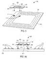
- FIG. 3illustrates a planar view of an exemplary embodiment of an RF ID tag according to the present invention.
- FIG. 4Aillustrates a cross-sectional view of an exemplary embodiment of an RF ID tag according to the present invention.
- FIG. 4Billustrates a cross-sectional view of an exemplary embodiment of an FR ID tag wherein the flexible strap has an additional cover.
- FIGS. 5–6illustrate of an exemplary embodiment of an RF ID tag according to the present invention.
- FIGS. 7A–Billustrate an exemplary embodiment of a signage display having the IC included in the flexible strap.
- FIGS. 8A–Billustrate an exemplary display of the present invention.
- FIG. 1illustrates an exemplary embodiment of an object that is functional component block 1 .
- Block 1has a top surface 2 upon which a circuit element is situated (not shown).
- the circuit element on the top surface 2may be an ordinary integrated circuit (IC) for any particular function.
- the ICmay be designed to drive a pixel of a display.
- the ICmay also be designed to receive power from another circuit for the operation of a passive RF ID tag.
- the ICmay be designed to receive power from an energy source (e.g. battery) for the operation of an active RF ID tag.
- block 1has a trapezoidal cross-section where the top of the block is wider than the bottom of the block 1 .
- Block 1may be created from a host substrate and separated from this substrate. This method of making block 1 can be found in the method described in copending U.S. patent application Ser. No. 09/251,220 now U.S. Pat. No. 6,291,896 referenced above. This patent is hereby incorporated by reference.
- FIG. 2illustrates an exemplary embodiment in which block 1 is deposited in a recessed region of a carrier substrate 12 .
- the block 1is recessed below a surface 32 of the carrier substrate 12 .
- the surface 32 of the carrier substrate 12is the native surface of the substrate before any deposition of any other materials on top of the surface 32 .
- Carrier substrate 12may be a flexible substrate made out of plastic, fabric, metal, or some other suitable materials. In a preferred embodiment, carrier substrate 12 is flexible.
- FIG. 2shows a planar view of a web material of carrier substrate 12 having recessed regions or holes 21 therein. These recessed regions or holes 21 may be created by a variety of methods.
- the regions or holes 21may be created by a web wheel, roller, or template, that have protruding structures as described in U.S. patent application Ser. No. 09/270,165, entitled “Apparatuses and Methods for Forming Assemblies” by Jeffrey Jay Jacobsen. This patent application is hereby incorporated by reference.
- Another methodinvolves using a template having blocks wherein the blocks are pressed into web material making recessed regions or holes 21 into the web material of carrier substrate 12 . (See U.S. patent application Ser. No. 09/270,157, entitled “Methods for Transferring Elements From a Template to a Substrate” describing the donor transfer method).
- the blocks 1may be deposited into the recessed regions or holes 21 of a carrier substrate 12 by a method described in U.S. Pat. No. 5,545,291. The block 1 is then being recessed within the carrier substrate 12 and below the surface 32 of the carrier substrate 12 .
- the U.S. Pat. No. 5,545,291explained how to assemble microstructures onto a substrate, and it is thus, incorporated herein by reference.
- This processmay be referred to as FSA (fluidic self assembly) and may be performed with a web material such as the web material for carrier substrate 12 .
- a web materialis advanced through a web process apparatus.
- the FSA processdeposits a plurality of blocks onto the web material wherein the blocks fall into recessed regions found in the web material.
- FIG. 2also shows a planar view of the web material of carrier substrate 12 wherein the blocks 1 are seated in the recessed regions or holes 21 .
- electrical interconnect 30is deposited onto the carrier substrate 12 interconnecting the top surface 2 of each block 1 to each other.
- the web material of carrier substrate 12is advanced to a further point in the FSA process wherein an interconnect layer is deposited thereon.
- the interconnect 30may be comprised of conductive polymers, metals (e.g., aluminum, copper, silver, gold, etc.), metal particles, conductive organic compounds, or conductive oxides.
- An insulation layer 31which is a dielectric material, may be coated over the area that have the interconnect 30 to prevent short circuit with other functional components that the carrier substrate 12 may come into contact with.
- the insulation layer 31insulates the circuit elements within the block 1 as well as the interconnect 30 that connects one block 1 to another block 1 .
- the insulation layer 31enables the carrier substrate 12 to cross over at least one electrical interconnection (e.g., another interconnect 30 on another substrate, or an antenna loop) without shorting out the whole device.
- the interconnect 30may be flexible interconnect layers (not shown). These interconnect layers may be made with the techniques used to create Tape Automated Bonding (TAB) tape interconnections well practiced in the semiconductor industry.
- TABTape Automated Bonding
- the flexible interconnect layersmay be created from one of numerous types of materials which are appropriate for a web tape material which is designed to hold electrically conductive interconnect layers. These materials include polyimide tapes on which are deposited conductive traces of metal. The metal may be deposited directly on the tape (e.g. by a blanket deposition) and then patterned by etching, or a photoresist layer may be applied and patterned, leaving grooves into which metal may be deposited.
- the interconnectmay be patterned to create an intricate wiring pattern such as row and/or column interconnects for an active matrix display backplane. The actual patterns will depend on the particular application for these functional components.
- the flexible interconnect layer, once created,may be applied to the carrier substrate 12 .
- the flexible interconnect layermay be fabricated in a web process and then aligned with the web material of carrier substrate 12 having blocks 1 either in a web process or outside of a web process.
- the carrier substratemay be flexible, planar, or rigid and made in a web process or batch process.
- an alignment operationusing conventional techniques, may be necessary to properly align the interconnect layer 30 relative to the carrier substrate 12 with blocks when the interconnect layer is coupled to the carrier substrate 12 .
- the process of interconnecting the functional components (e.g., blocks 1 ) embedded in a substrateuses only a single layer of metalization for interconnect layer 30 . This will reduce the possibility of interlayer shorts on the electronic devices.
- FIG. 3illustrates an exemplary embodiment of an RF ID tag 300 .
- a flexible carrier strap 301comprising functional components is coupled to a receiving substrate 310 , also comprising functional components.
- the flexible strap 301may be the carrier substrate 12 discussed in FIG. 2 above.
- the flexible strap 301comprises at least one functional component 302 .
- the functional component 302is much like the functional component block 1 of FIG. 1 .
- the flexible strap 301also may comprise other necessary components 303 and 304 such as a resistor, a capacitor or an inductor for completing the necessary circuitry. Components 303 and 304 may also be manufactured as blocks 1 above.
- Components 302 , 303 and 304may be interconnected, typically, through metal connectors such as metal wires, thin evaporated layer of conductor material (e.g., Aluminum) or ink containing metals (not shown). The interconnection of all the components can be achieved with the interconnects 30 discussed above.
- metal connectorssuch as metal wires, thin evaporated layer of conductor material (e.g., Aluminum) or ink containing metals (not shown).
- the interconnection of all the componentscan be achieved with the interconnects 30 discussed above.
- Flexible strap 301further includes at least two carrier connection pads 305 and 306 .
- the carrier connection pads 305 and 306are used to couple the flexible strap 301 to the receiving substrate 310 (see below).
- the carrier connection pads 305 and 306are made out of conductive materials.
- a conductive adhesivecan be used to couple the flexible strap 301 to the receiving substrate 310 thereby establishing electrical interconnections for all of the functional components from the flexible strap 301 to those from the receiving substrate 310 .
- the methods called cold swaging or ultrasonic weldingwhich, are well practiced in the field, can be used to couple the flexible strap 301 to the receiving substrate 310 .
- the receiving substrate 310includes an antenna 311 as a functional component.
- the receiving substrate 310may be flexible and made out of some low cost plastic or some other suitable material for the particular application.
- the receiving substrate 310is preferably planar.
- the antenna 311may be loops of wire attached to the receiving substrate 310 .
- the antenna 311may also be made out of screen printed conductors such as silver, carbon, or metal that is coupled to the receiving substrate 310 that has been etched with patterns to receive the antenna material.
- the antenna 311may also be made out of laminated drawn foil that has an adhesive containing layer which enables the antenna to be coupled to the receiving substrate 310 in any particular pattern, for instance, loops.
- receiving connection pad 312 and 313At each end of the loops of the antenna 311 , there is a receiving connection pad, in this embodiment, receiving connection pads 312 and 313 .
- the receiving connection pads 312 and 313are also made out of conductive materials to establish the conductive connection for all of the functional components from the receiving substrate 310 to those from the flexible strap 301 .
- the flexible strap 301is coupled to the receiving substrate 310 .
- the coupling of the flexible strap 301 and the receiving substrate 310is achieved through the attachment of the carrier connection pads 305 and 306 to the receiving connection pads 312 and 313 as shown by arrows A and B.
- the flexible strap 301can cross over at least one conducting material.
- the flexible strap 301crosses the loops of the antenna ( FIG. 5 ).
- a conductive adhesiveis used to couple all of the carrier connection pads to the receiving connection pads.
- the flexible substrate 310may have other functional components or other circuitries, instead of or in addition to the antenna 311 .
- another functional component like blocks 1which may have circuitries designed to drive display pixel electrodes, to draw energy source, to sense external inputs, or to transfer data.
- the total carrier connection pads(such as 305 and 306 ) is only two even if there are multiple functional components in the flexible strap 301 .
- FIG. 4Aillustrates the cross-sectional view of the embodiment described in FIG. 3 .
- This figureshows in details that there is preferably an insulation layer 402 between the metal wires 401 that interconnect all of the components on the flexible strap 301 and the antenna 311 on the receiving substrate 310 .
- the insulation layer 402is a dielectric material that serves to electrically isolate the metal wires on flexible substrate 301 and the antenna 311 on the receiving substrate 310 . Contacting the metal wires 401 with the antenna or the electrical circuitry will short-circuit the antenna or other the electrical circuitry.
- the flexible strap 301can be covered with a protected layer 404 for extra protection ( FIG. 4B ).
- the protected layer 404can be made out of any flexible material such as polymer or plastic.
- the protected layer 404can also be transparent or opaque.
- the method of fabricating the electronic devices described in FIGS. 3 , 4 A and 4 Bcan be applied to make a wide range of other electronic devices.
- the small flexible strap 301 with blocks 1can be made to be readily available components that can be used for any particular purpose.
- the flexible strap 301can be used in the fabrication of display components, micro-electro-mechanical structural elements, or generally, an assembly of sensors or actuators or an assembly of circuit elements.
- devicessuch as flexible antennas, other sensors, detectors, or an array of circuit elements may be fabricated using one of the embodiments of the inventions.
- blocks 1are made with very small silicon or other materials suitable for carrying a circuit.
- Making blocks 1 small(in the order of tens of micrometers in dimension) optimizes the expensive technology and the expensive media materials necessary (e.g., silicon wafer) to fabricate these blocks 1 .
- Making the blocks 1 smallalso enables the functional components to be small, thus, saving material cost as well as the processing cost.
- small blocks 1enable small packaging of the silicon material which means more of blocks 1 can be produced at a higher rate with less materials.
- flexible strap 301may be viewed as an interposer which is an intermediate that bridge functional components of radically different densities together without the waste of materials.
- the functional component that is the most expensive to fabricatecan be made like the blocks 1 which is very small in dimension.
- the blocks 1are then deposited into the flexible strap 301 , and then integrated with another functional components that can be made out of a cheaper material or technology. More importantly, we can optimize the most expensive technology, i.e., the interconnecting technology, where it is needed.
- the expensive interconnecting technology(e.g., FSA) is only used in making the flexible strip 301 while the making of the antenna, for example, can be achieved using a lower cost interconnecting technology.
- FSAexpensive interconnecting technology
- the functional block 14has a total size of 350 ⁇ m ⁇ 500 ⁇ m (width ⁇ length) with a design feature size or design rule of 0.5 ⁇ m.
- the flexible strap 301as a total size of 1.5 mm ⁇ 10 mm with a design feature size of 20 ⁇ m.
- the receiving substrate 311has the total size of 20 mm ⁇ 50 mm with the design feature size of 250 ⁇ m.
- the design feature size or design rulecan be thought of as a density for each of the components. The embodiments discussed therefore, enable the integrating and the interfacing of radically different density electronic devices to each other without wastes of expensive material and technology.
- FIG. 5illustrates an example of an RF ID tag 500 made using the method described in FIGS. 3 , 4 A and 4 B.
- Current artincludes RF ID tags, which are small, nevertheless, contains very limited information due to the size constraint. Also, current RF ID tags are inflexible because the IC packagings are rigid and large. Storing more information also means that the RF ID tag would have to have more functional components and as a result, require more interconnections among different functional components. Placing these many functional components on the same substrate is overly expensive and complex, not to mention increasing the chance for short circuit in the system. For a flexible and thin RF ID tag, it is desirable to have the silicon integrated circuitry (IC) be small and thin.
- the blocks 1 described abovemay be used to contain the IC which can then be incorporated into the RF ID tag 500 .
- the RF ID tag 500can be placed on products such as store merchandise as a way to label, identify, and track these products.
- FIG. 5illustrates an example of depositing the all of the functional components except for the antenna 311 onto the flexible strap 301 and using the flexible strap 301 to bridge the antenna 311 .
- FIG. 6is an enlarged view of the flexible strap that is used in the RF ID tag 500 .
- the antenna 311would be deposited on receiving substrate 310 , typically a thick material.
- the functional components(not shown) would then be deposited in area 500 .
- Some conductive materialwould interconnect the functional components to each other.
- a strapwould bridge one side of the loops of the antenna 311 to the other side of the loops of.
- the straphas no function other than to complete the circuit for the antenna 311 .
- Under the current artif there is a defective functional components, that will not be detected until the whole fabrication of the RF ID tag 500 is completed. When that happens, materials are wasted since the whole RF ID tag is discarded. Furthermore, the alignment of these functional components makes the assembly process complicated and expensive.
- the functional componentswould be placed in the flexible strap 301 and not area 500 .
- the flexible strap 301would serve to bridge one side of the antenna 311 to the other side of the antenna 311 .
- the flexible strap 301would carry the functional components that have particular functions, for instance, to receive power for the operation of the RF ID tag 500 or to send information to a base station of the RF ID tag base 500 .
- a low cost technologysuch as screen-printing can be used to produce large area elements such as the antenna 311 .
- the antenna 311may be printed in massive quantity on some low cost substrate and using a process that requires less rigorous alignment.
- the functional componentsuch as the blocks 1 to drive the antenna 311 or to send the data from the RF ID tag 500 , may be as described in U.S. patent application Ser. No. 09/251,220 mentioned above.
- the blocks 1are then integrated into the carrier substrate 12 with a high precision and more expensive technology such as the fluidic self-assembly.
- the small flexible strap 301can be used to carry all of the essential components that are expensive to manufacture.
- the expensive interconnecting technologyis optimized in that all of the essential components are packaged into the flexible strip 301 which is then coupled to the antenna that would be made out of a lower cost interconnecting technology.
- FIGS. 7A–7Billustrate a general view of a signage display utilizing the flexible strap 301 of the present invention.
- the display system 700includes a flexible strap 701 , which is similar to the flexible strap 301 described above, a top electrode layer 710 , a viewable area 720 , and a backplane layer 730 .
- a general display systemhave its electronic circuit elements, such as row or column driver circuits, attached to flexible circuits such as TAB tape. The assembly is then attached to the LCD on one side and a PC board on the other. An additional set of circuits is usually added to the second glass or plastic layer.
- the driver circuitsare attached to each glass or plastic substrate; in an active matrix LCD, the driver circuits are attached to two or four edges on only one of the glass or plastic substrates. These drive circuits provide the electrical control signals and data required to form an image on the LCD. While an LCD is used for the example, the same principles apply to other display media such as plasma, electroluminescence, electrophoretic, electrochromic, and the like.
- the flexible strap 701includes at least one integrated circuit which is embedded in a functional block 702 .
- the functional block 702is manufactured as one of the blocks 1 discussed above.
- the functional block 702may be manufactured according to the method disclosed in the U.S. patent application Ser. No. 09/671,659, entitled “Display Devices and Integrated Circuits” which was filed on Sep. 27, 2000, by inventors Roger Green Stewart, et. al. This patent application is incorporated by reference herein.
- the functional block 702is interconnected to eight output pads, 703 a , 703 b , 703 c , 703 d , 703 e , 703 f , 703 g , and 703 h .
- Each of these output padsis responsible for driving a particular segment of the display system. And, each of the segment displays a particular image of the signage display.
- the functional block 702may also include an output pad 705 for a ground signal, or other necessary function for an integrated circuit.
- Each of these output pads 703 a , 703 b , 703 c , 703 d , 703 e , 703 f , 703 g , and 703 hfunctions like those carrier connection pads 305 and 306 .
- these padsestablish electrical connections between the integrated circuit included in the functional component 702 and the functional components on the display.
- the output pad 703 gmay be used to establish the electrical connection with the portion of the top electrode layer 710 that is responsible for controlling the “Jones Product” segment of the display system 700 .
- the output pad 703 emay be used to establish the electrical connection with the portion of the top electrode layer 710 that is responsible for controlling the “Creations” segment of the display system 700 .
- the output pads 703 a , 703 b , 703 c , 703 d , 703 e , 703 f , 703 g , and 703 hall establishes electrical connections with the top electrode layer 710 that in turn drives the segments of the display system 700 .
- the flexible strap 701is coupled to the backplane layer 730 of the display system 700 .
- a thin layer of nonconductive adhesivemay be coated over the carrier substrate 704 .
- the adhesivewould be coated over the all of the area that do not have the output pads 703 a , 703 b , 703 c , 703 d , 703 e , 703 f , 703 g , and 703 h .
- the flexible strap 701may be affixed to a surface such as the backplane layer 730 while the electrical function of the output pads 703 a , 703 b , 703 c , 703 d , 703 e , 703 f , 703 g , and 703 h would not be blocked by the adhesive layer. These outputs pads therefore, would be able to establish the necessary electrical connections with the top electrode layer 710 .
- the output pads 703 a , 703 b , 703 c , 703 d , 703 e , 703 f , 703 g , and 703 hare all made out of conductive adhesive such that when affixed to the top electrode layer 701 , these pads can establish both the mechanical as well as the electrical contact to the electrode layer 701 .
- the number of the output padsdepends on the particular applications or the displays.
- the number of the output padsmay be more or less than eight output pads for each functional component block.
- larger signage displaycan also be made using the examples discussed above. For instance, when the signage display requires more segments or portions for larger images, more functional blocks 1 can be incorporated into the flexible strap 701 .
- the flexible straps 701 a , 701 b , 701 c , and 701 dare coupled to the backplane layer 730 of the display system 700 - 2 .
- a thin layer of nonconductive adhesivemay be coated over the carrier substrate 704 a , 704 b , 704 c , and 704 d .
- the adhesivewould be coated over the all of the area that do not have the output pads.
- the flexible straps 701 a , 701 b , 701 c , and 701 dmay be affixed to the backplane layer 730 and the adhesive layer would not block the electrical function of the associated output pads. These output pads therefore, would be able to establish the necessary electrical connections with the top electrode layer 710 for the display 700 .
- FIG. 8Ashows an overview of a display system 800 , which can be the signage display 700 in FIGS. 7A–7B .
- FIG. 8Aillustrates a planar view of the display system 800
- FIG. 8Billustrates a cross-sectional view of the display system 800 .
- the display system 800comprises of a carrier substrate 802 , which includes integrated circuits, for example, block 1 , for driving the display.
- carrier substrate 802is flexible and small.
- the carrier substrate 802is considerably smaller than the receiving substrate 801 .
- the carrier substrate 802is coupled to pixel electrodes 801 A– 801 D on a receiving carrier substrate 801 through the couplings of connection pads, for instance connection pad 806 A to 807 A, connection pad 806 B to 807 B, connection pad 806 C to 807 C, and connection pad 806 D to 807 D. These couplings would enable the integrated circuit to drive the pixel electrodes 800 A– 800 D in the display system 800 .
- the display system 800also comprises insulation layer, display material, and counter electrode or cover glass electrode. They are discussed in details below.
- FIG. 8Bshows a cross-sectional view of the display system 800 according to one embodiment of the present invention.
- the display system 800includes a carrier substrate 802 , which has receiving openings for functional components such as integrated circuits 802 A, 802 B, and 802 C.
- the carrier substrate 802is made using the embodiment discussed above for flexible strip 301 in FIG. 3 . Similar to the embodiments discussed above, the functional components once coupled to the carrier substrate are recessed within the carrier substrate and below the native surface of the carrier substrate.
- the carrier substrate 802also includes carrier connection pads 806 A–D, which establish mechanical as well as electrical connections with the receiving substrate 801 .
- the receiving substrate 801can be made using a coarse technology and some coarse materials for making signage display.
- the display system 800includes a receiving substrate 801 which further comprising pixel electrodes 801 A– 801 D.
- the receiving substrate 801also comprises receiving connection pads 807 A–D.
- the receiving connection pads 807 A–Dare interconnected with the pixel electrodes 801 A–D and thus, when coupled to the carrier connection pads 806 A–D, establish mechanical as well as electrical connections with the carrier substrate 802 . Similar to the embodiments discussed above, the carrier substrate 802 can cross over at least one electrical interconnection on the receiving substrate 801 without damaging or shorting the pixel electrodes on the receiving substrate 801 .
- the carrier connection pads 806 A–Dare also interconnected with the ICs 802 A, 802 B and 802 C. When all the necessary connections are established, the ICs will then drive the pixel electrode of the signage display 800 .
- the integrated circuits 802 A, 802 B, and 802 Care display drivers in one embodiment. When proper mechanical and electrical connections are established, these integrated circuits will drive the pixel electrodes in the display system 800 .
- the carrier substrate 802may be made out of a metal, foil, or flexible plastic material.
- An insulating layer 805maybe attached to a top surface of the carrier substrate 802 .
- the insulating layer 805has a plurality of openings through which electrical interconnections can be established (e.g., vias through which carrier connection pads 806 A–D interconnect with receiving connection pads 807 A–D).
- a layer 808may be provided on top of the pixels electrodes and the conductive signals electrodes in order to insulate these parts from the display media material 803 which may be a nematic liquid crystal, an electrophoretic display material, a polymer dispersed liquid crystal material, an organic light emitting diode material, a cholesteric liquid crystal material, an electrochromic material, a particle-based material, a thin-film electroluminescent material, or other known display materials which can be driven by pixel electrodes or other types of display materials which may be controlled by electrodes.
- a counter electrode or cover glass electrode 804is typically a thin layer of transparent indium tin oxide which is deposited upon a cover glass 900 which is transparent. Spacers 809 are attached to the layer 808 and to the cover glass 900 to provide a desired spacing between the counter electrode 804 and the layer 808 .
- carrier substrate 802acts as an interposer that integrates or interfaces two radically different feature sized electrical devices to each other (e.g., integrating the micro display drivers to the large signage display).
- the methods described aboveallow the ICs to be manufactured in the order of sub-micrometer density.
- the methods abovethen enable the integration of the sub-micrometer ICs to a much coarser and larger display. Using this method, the ICs do not need to be made large in order to facilitate the coupling of the ICs into a large display panel. Expensive materials and technologies are thus optimized. This provides for greatly reduced manufacturing costs and improved yield and efficiency in the manufacturing process.
- Displays according to the present inventionmay be used to fabricate displays with liquid crystals, polymer dispersed liquid crystal, electroluminescent (EL) materials, organic light emitting diodes (OLEDs), up and downconverting phosphor (U/DCP), electrophoretic (EP) materials, or light emitting diodes (LEDs).
- ELelectroluminescent
- OLEDorganic light emitting diodes
- U/DCPup and downconverting phosphor
- EPelectrophoretic
- LEDslight emitting diodes
- Display panelsmay be comprised of active matrix or passive matrix. Active matrix panels and passive matrix panels may be either transmissive or reflective.
- LCDsLiquid crystal displays
- display system 800can have an active-matrix backplane in which thin-film transistors are co-located with LCD pixels.
- Flat-panel displays employing LCDsgenerally include five different components or layers.
- a light sourcea first polarizing filter that is mounted on one side of a circuit panel on which the thin-film transistors are arrayed to form the pixels such as pixels 801 A– 801 D.
- a filter plate containing at least three primary colorsare aligned with the pixels (for color displays), and a second polarizing filter.
- a volume between the circuit panel and the filter plateis filled with liquid crystal material, for instance, layer 803 .
- This materialwill rotate the polarized light when an electric field is applied between the thin-film transistor circuit panel and a electrodes affixed to the filter plate or a cover glass.
- the liquid crystal materialrotates polarized light being transmitted through the material so that it will pass through the second polarizing filter.
- Some liquid crystal materialsrequire no polarizers.
- LCDsmay also have a passive matrix backplane which is usually two planes of strip electrodes which sandwich the liquid crystal material.
- passive matricesgenerally provide a lower quality display compared to active matrices.
- U/DCP and EP displaysare formed in similar fashion except the active medium is different (e.g., upconverting gas, downconverting gas, electrophoretic materials).
- EL displayshave one or more pixels that are energized by an alternating current (AC) that must be provided to each pixel by row and column interconnects.
- EL displaysgenerally provide a low brightness output because passive circuitry for exciting pixel phosphors typically operates at a pixel excitation frequency that is low relative to the luminance decay time of the phosphor material.
- an active matrixreduces the interconnect capacitance allowing the use of high frequency AC in order to obtain more efficient electroluminescence in the pixel phosphor. This results in increased brightness in the display.
- LED displaysare also used in flat-panel displays. LEDs emit light when energized. OLEDs operate like the LEDs except OLEDs use organic material in the formation of the light emitting device.
- the displays discussed aboveare particularly useful for signage displays used in airport terminal, commercial signage display, or billboard displays. These types of displays are typically large and the manufacturing of the display panel is relatively cheap due to the fact that they employ a less rigorous technology with large feature sizes. However, the integrated circuit needed to drive these types of displays are expensive to make and have small feature sizes.
- the method of this inventionallows the manufacturers to make the IC very small and still connect them to the large signage display.
- the flexible strap 301is particularly crucial for integrating and interfacing electronic devices of radically different feature sizes. Integrating and interfacing the blocks 1 to a coarse and large display requires the blocks 1 to be large enough in order for the integrating and the interfacing to be feasible. However, to minimize cost in making the IC, the blocks 1 are very small in feature size, for example, the blocks 1 have a densities in the vicinity of sub-micrometer.
- the signage displayis typically in the order of 100–250 micrometer in density. One way to efficiently integrating and interfacing the signage display to the blocks 1 is through using the carrier substrate discussed above for the flexible strap 301 .
- the functional block 1has a total size of 350 ⁇ m ⁇ 500 ⁇ m (width ⁇ length) with a design feature or design rule of 0.5 ⁇ m.
- the carrier substrate 802has a total size of 10 mm ⁇ 10 mm with a design feature of 201 ⁇ m.
- the receiving substrate 801has the total size of 20 in ⁇ 50 in with the design feature of 250 ⁇ m.
- the carrier substrateis thus about one order of magnitude different from the functional block 1 and an order of magnitude different from the signage display.
- An electrical device made according to the embodiments of the present inventionalso has an advantage of being multi-feature-size.
- the carrier substrate 12may have a feature size (design rule) that is at least five times larger than the block 1 .
- the carrier substrate 12also has a feature size that is at least five times smaller than the receiving substrate 310 .
- the functional block 1can be packaged in a flexible strap, the carrier substrate discussed above.
- Flexible packagingalso means that these signage displays can be made flexible which is extremely useful for many purposes. It also means that the sign can be very thin, owing to the thin dimension of the flexible strap.
- An electrical device made according to the embodiments of the present inventionalso has all of the electrical circuitry in the functional components and the necessary interconnections, (e.g., the first interconnection and the second interconnection) are all essentially in coplanar to each other. As can be seen from FIG. 3 and FIG. 5 , when the whole device is assembled together, all of the components mentioned above are essentially in one plane field. Alternatively, all of the electrical circuitry in the functional components and the necessary interconnection, (e.g., the first interconnection and the second interconnection) each forms a plane that is separated from one another by less than ten micrometers. Therefore the planar electrical circuitry on the functional component, the planar first interconnection on the carrier substrate, and the planer second interconnection on the receiving substrate are all coplanar with each other such that their planes are typically separated by less than 10 micrometers.
Landscapes
- Engineering & Computer Science (AREA)
- Microelectronics & Electronic Packaging (AREA)
- Computer Hardware Design (AREA)
- Physics & Mathematics (AREA)
- General Physics & Mathematics (AREA)
- Theoretical Computer Science (AREA)
- Power Engineering (AREA)
- Computer Networks & Wireless Communication (AREA)
- Manufacturing & Machinery (AREA)
- Devices For Indicating Variable Information By Combining Individual Elements (AREA)
- Combinations Of Printed Boards (AREA)
Abstract
Description
Claims (31)
Priority Applications (4)
| Application Number | Priority Date | Filing Date | Title |
|---|---|---|---|
| US10/952,201US6985361B2 (en) | 2001-05-31 | 2004-09-27 | Electronic devices with small functional elements supported on a carrier |
| US11/188,149US7260882B2 (en) | 2001-05-31 | 2005-07-22 | Methods for making electronic devices with small functional elements supported on a carriers |
| US11/824,959US7559131B2 (en) | 2001-05-31 | 2007-07-02 | Method of making a radio frequency identification (RFID) tag |
| US12/502,888US8516683B2 (en) | 2001-05-31 | 2009-07-14 | Methods of making a radio frequency identification (RFID) tags |
Applications Claiming Priority (3)
| Application Number | Priority Date | Filing Date | Title |
|---|---|---|---|
| US09/872,985US6606247B2 (en) | 2001-05-31 | 2001-05-31 | Multi-feature-size electronic structures |
| US10/464,031US6816380B2 (en) | 2001-05-31 | 2003-06-17 | Electronic devices with small functional elements supported on a carrier |
| US10/952,201US6985361B2 (en) | 2001-05-31 | 2004-09-27 | Electronic devices with small functional elements supported on a carrier |
Related Parent Applications (1)
| Application Number | Title | Priority Date | Filing Date |
|---|---|---|---|
| US10/464,031DivisionUS6816380B2 (en) | 2001-05-31 | 2003-06-17 | Electronic devices with small functional elements supported on a carrier |
Related Child Applications (1)
| Application Number | Title | Priority Date | Filing Date |
|---|---|---|---|
| US11/188,149ContinuationUS7260882B2 (en) | 2001-05-31 | 2005-07-22 | Methods for making electronic devices with small functional elements supported on a carriers |
Publications (2)
| Publication Number | Publication Date |
|---|---|
| US20050270752A1 US20050270752A1 (en) | 2005-12-08 |
| US6985361B2true US6985361B2 (en) | 2006-01-10 |
Family
ID=25360749
Family Applications (6)
| Application Number | Title | Priority Date | Filing Date |
|---|---|---|---|
| US09/872,985Expired - LifetimeUS6606247B2 (en) | 2001-05-31 | 2001-05-31 | Multi-feature-size electronic structures |
| US10/464,031Expired - LifetimeUS6816380B2 (en) | 2001-05-31 | 2003-06-17 | Electronic devices with small functional elements supported on a carrier |
| US10/952,201Expired - LifetimeUS6985361B2 (en) | 2001-05-31 | 2004-09-27 | Electronic devices with small functional elements supported on a carrier |
| US11/188,149Expired - Fee RelatedUS7260882B2 (en) | 2001-05-31 | 2005-07-22 | Methods for making electronic devices with small functional elements supported on a carriers |
| US11/824,959Expired - Fee RelatedUS7559131B2 (en) | 2001-05-31 | 2007-07-02 | Method of making a radio frequency identification (RFID) tag |
| US12/502,888Expired - Fee RelatedUS8516683B2 (en) | 2001-05-31 | 2009-07-14 | Methods of making a radio frequency identification (RFID) tags |
Family Applications Before (2)
| Application Number | Title | Priority Date | Filing Date |
|---|---|---|---|
| US09/872,985Expired - LifetimeUS6606247B2 (en) | 2001-05-31 | 2001-05-31 | Multi-feature-size electronic structures |
| US10/464,031Expired - LifetimeUS6816380B2 (en) | 2001-05-31 | 2003-06-17 | Electronic devices with small functional elements supported on a carrier |
Family Applications After (3)
| Application Number | Title | Priority Date | Filing Date |
|---|---|---|---|
| US11/188,149Expired - Fee RelatedUS7260882B2 (en) | 2001-05-31 | 2005-07-22 | Methods for making electronic devices with small functional elements supported on a carriers |
| US11/824,959Expired - Fee RelatedUS7559131B2 (en) | 2001-05-31 | 2007-07-02 | Method of making a radio frequency identification (RFID) tag |
| US12/502,888Expired - Fee RelatedUS8516683B2 (en) | 2001-05-31 | 2009-07-14 | Methods of making a radio frequency identification (RFID) tags |
Country Status (4)
| Country | Link |
|---|---|
| US (6) | US6606247B2 (en) |
| EP (1) | EP1399879A1 (en) |
| JP (1) | JP2005518000A (en) |
| WO (1) | WO2002097724A1 (en) |
Cited By (46)
| Publication number | Priority date | Publication date | Assignee | Title |
|---|---|---|---|---|
| US20060109130A1 (en)* | 2004-11-22 | 2006-05-25 | Hattick John B | Radio frequency identification (RFID) tag for an item having a conductive layer included or attached |
| US20060109123A1 (en)* | 2004-11-22 | 2006-05-25 | Curt Carrender | Radio frequency identification (RFID) tag for an item having a conductive layer included or attached |
| US20060267778A1 (en)* | 2003-03-24 | 2006-11-30 | Gengel Gleen W | RFID tags and processes for producing RFID tags |
| US20070031992A1 (en)* | 2005-08-05 | 2007-02-08 | Schatz Kenneth D | Apparatuses and methods facilitating functional block deposition |
| US20070075866A1 (en)* | 2005-10-04 | 2007-04-05 | Hohler Donald W | Apparatus for encapsulating radio frequency identification (RFID) antennae |
| US20070216534A1 (en)* | 2002-12-31 | 2007-09-20 | Ferguson Scott W | Rfid device and method of forming |
| US20070256291A1 (en)* | 2001-05-31 | 2007-11-08 | Credelle Thomas L | Electronic devices with small functional elements supported on a carrier |
| US20090109035A1 (en)* | 2007-10-10 | 2009-04-30 | Vivek Subramanian | High Reliability Surveillance and/or Identification Tag/Devices and Methods of Making and Using the Same |
| US20090178709A1 (en)* | 2008-01-15 | 2009-07-16 | General Electric Company | Solar cell and magnetically self-assembled solar cell assembly |
| US20090230380A1 (en)* | 2007-12-14 | 2009-09-17 | Nanosys, Inc. | Methods for Formation of Substrate Elements |
| US20090283886A1 (en)* | 2003-08-29 | 2009-11-19 | Semiconductor Energy Laboratory Co., Ltd. | Ic card |
| US20090320139A1 (en)* | 2004-11-22 | 2009-12-24 | Curt Carrender | Transponder incorporated into an electronic device |
| US20100068839A1 (en)* | 2007-05-31 | 2010-03-18 | Nthdegree Technologies Worldwide Inc. | Method of Manufacturing a Light Emitting, Photovoltaic or Other Electronic Apparatus and System |
| US8133768B2 (en) | 2007-05-31 | 2012-03-13 | Nthdegree Technologies Worldwide Inc | Method of manufacturing a light emitting, photovoltaic or other electronic apparatus and system |
| US8182303B2 (en) | 2004-12-27 | 2012-05-22 | Nthdegree Technologies Worldwide Inc | Method of fabricating static and addressable emissive displays |
| US8349653B2 (en) | 2010-06-02 | 2013-01-08 | Maxim Integrated Products, Inc. | Use of device assembly for a generalization of three-dimensional metal interconnect technologies |
| US8415879B2 (en) | 2007-05-31 | 2013-04-09 | Nthdegree Technologies Worldwide Inc | Diode for a printable composition |
| US8413359B2 (en) | 2008-05-13 | 2013-04-09 | Nthdegree Technologies Worldwide Inc | Illuminating display systems |
| US8674593B2 (en) | 2007-05-31 | 2014-03-18 | Nthdegree Technologies Worldwide Inc | Diode for a printable composition |
| US8712233B2 (en) | 2012-02-24 | 2014-04-29 | Apple Inc. | Electronic device assemblies |
| US8739441B2 (en) | 2008-05-13 | 2014-06-03 | Nthdegree Technologies Worldwide Inc | Apparatuses for providing power for illumination of a display object |
| US8766858B2 (en) | 2010-08-27 | 2014-07-01 | Apple Inc. | Antennas mounted under dielectric plates |
| US8809126B2 (en) | 2007-05-31 | 2014-08-19 | Nthdegree Technologies Worldwide Inc | Printable composition of a liquid or gel suspension of diodes |
| US8846457B2 (en) | 2007-05-31 | 2014-09-30 | Nthdegree Technologies Worldwide Inc | Printable composition of a liquid or gel suspension of diodes |
| US8852467B2 (en) | 2007-05-31 | 2014-10-07 | Nthdegree Technologies Worldwide Inc | Method of manufacturing a printable composition of a liquid or gel suspension of diodes |
| US8877101B2 (en) | 2007-05-31 | 2014-11-04 | Nthdegree Technologies Worldwide Inc | Method of manufacturing a light emitting, power generating or other electronic apparatus |
| US8889216B2 (en) | 2007-05-31 | 2014-11-18 | Nthdegree Technologies Worldwide Inc | Method of manufacturing addressable and static electronic displays |
| US9018833B2 (en) | 2007-05-31 | 2015-04-28 | Nthdegree Technologies Worldwide Inc | Apparatus with light emitting or absorbing diodes |
| US9318793B2 (en) | 2012-05-02 | 2016-04-19 | Apple Inc. | Corner bracket slot antennas |
| US9343593B2 (en) | 2007-05-31 | 2016-05-17 | Nthdegree Technologies Worldwide Inc | Printable composition of a liquid or gel suspension of diodes |
| US9419179B2 (en) | 2007-05-31 | 2016-08-16 | Nthdegree Technologies Worldwide Inc | Diode for a printable composition |
| US9425357B2 (en) | 2007-05-31 | 2016-08-23 | Nthdegree Technologies Worldwide Inc. | Diode for a printable composition |
| US9455489B2 (en) | 2011-08-30 | 2016-09-27 | Apple Inc. | Cavity antennas |
| US9534772B2 (en) | 2007-05-31 | 2017-01-03 | Nthdegree Technologies Worldwide Inc | Apparatus with light emitting diodes |
| US9825202B2 (en) | 2014-10-31 | 2017-11-21 | eLux, Inc. | Display with surface mount emissive elements |
| US10236279B2 (en) | 2014-10-31 | 2019-03-19 | eLux, Inc. | Emissive display with light management system |
| US10242977B2 (en) | 2014-10-31 | 2019-03-26 | eLux, Inc. | Fluid-suspended microcomponent harvest, distribution, and reclamation |
| US10319878B2 (en) | 2014-10-31 | 2019-06-11 | eLux, Inc. | Stratified quantum dot phosphor structure |
| US10381335B2 (en) | 2014-10-31 | 2019-08-13 | ehux, Inc. | Hybrid display using inorganic micro light emitting diodes (uLEDs) and organic LEDs (OLEDs) |
| US10381332B2 (en) | 2014-10-31 | 2019-08-13 | eLux Inc. | Fabrication method for emissive display with light management system |
| US10418527B2 (en) | 2014-10-31 | 2019-09-17 | eLux, Inc. | System and method for the fluidic assembly of emissive displays |
| US10446728B2 (en) | 2014-10-31 | 2019-10-15 | eLux, Inc. | Pick-and remove system and method for emissive display repair |
| US10520769B2 (en) | 2014-10-31 | 2019-12-31 | eLux, Inc. | Emissive display with printed light modification structures |
| US10535640B2 (en) | 2014-10-31 | 2020-01-14 | eLux Inc. | System and method for the fluidic assembly of micro-LEDs utilizing negative pressure |
| US10543486B2 (en) | 2014-10-31 | 2020-01-28 | eLux Inc. | Microperturbation assembly system and method |
| US10672748B1 (en) | 2010-06-02 | 2020-06-02 | Maxim Integrated Products, Inc. | Use of device assembly for a generalization of three-dimensional heterogeneous technologies integration |
Families Citing this family (246)
| Publication number | Priority date | Publication date | Assignee | Title |
|---|---|---|---|---|
| US6674562B1 (en) | 1994-05-05 | 2004-01-06 | Iridigm Display Corporation | Interferometric modulation of radiation |
| US6680792B2 (en) | 1994-05-05 | 2004-01-20 | Iridigm Display Corporation | Interferometric modulation of radiation |
| US7138984B1 (en)* | 2001-06-05 | 2006-11-21 | Idc, Llc | Directly laminated touch sensitive screen |
| WO1999052006A2 (en) | 1998-04-08 | 1999-10-14 | Etalon, Inc. | Interferometric modulation of radiation |
| US8928967B2 (en) | 1998-04-08 | 2015-01-06 | Qualcomm Mems Technologies, Inc. | Method and device for modulating light |
| US6468638B2 (en) | 1999-03-16 | 2002-10-22 | Alien Technology Corporation | Web process interconnect in electronic assemblies |
| AU8321601A (en)* | 2000-08-11 | 2002-02-25 | Escort Memory Systems | Rfid tag assembly and system |
| US7501954B1 (en) | 2000-10-11 | 2009-03-10 | Avante International Technology, Inc. | Dual circuit RF identification tags |
| US6710541B2 (en)* | 2000-12-22 | 2004-03-23 | Reveo, Inc. | Polarized light sources and methods for making the same |
| US6951596B2 (en) | 2002-01-18 | 2005-10-04 | Avery Dennison Corporation | RFID label technique |
| US6967640B2 (en)* | 2001-07-27 | 2005-11-22 | E Ink Corporation | Microencapsulated electrophoretic display with integrated driver |
| US6731353B1 (en)* | 2001-08-17 | 2004-05-04 | Alien Technology Corporation | Method and apparatus for transferring blocks |
| US7218527B1 (en)* | 2001-08-17 | 2007-05-15 | Alien Technology Corporation | Apparatuses and methods for forming smart labels |
| KR20040105705A (en)* | 2002-01-23 | 2004-12-16 | 에이리언 테크놀로지 코포레이션 | Apparatus incorporating small-feature-size and large-feature-size components and method for making same |
| US7214569B2 (en)* | 2002-01-23 | 2007-05-08 | Alien Technology Corporation | Apparatus incorporating small-feature-size and large-feature-size components and method for making same |
| KR20030076274A (en)* | 2002-03-18 | 2003-09-26 | 도레 엔지니아린구 가부시키가이샤 | Non-contact id card and the method for producing thereof |
| US6665193B1 (en)* | 2002-07-09 | 2003-12-16 | Amerasia International Technology, Inc. | Electronic circuit construction, as for a wireless RF tag |
| US6915551B2 (en)* | 2002-08-02 | 2005-07-12 | Matrics, Inc. | Multi-barrel die transfer apparatus and method for transferring dies therewith |
| US7023347B2 (en)* | 2002-08-02 | 2006-04-04 | Symbol Technologies, Inc. | Method and system for forming a die frame and for transferring dies therewith |
| US6867983B2 (en)* | 2002-08-07 | 2005-03-15 | Avery Dennison Corporation | Radio frequency identification device and method |
| US6940408B2 (en)* | 2002-12-31 | 2005-09-06 | Avery Dennison Corporation | RFID device and method of forming |
| US7244326B2 (en)* | 2003-05-16 | 2007-07-17 | Alien Technology Corporation | Transfer assembly for manufacturing electronic devices |
| US7324061B1 (en) | 2003-05-20 | 2008-01-29 | Alien Technology Corporation | Double inductor loop tag antenna |
| US7223320B2 (en)* | 2003-06-12 | 2007-05-29 | Symbol Technologies, Inc. | Method and apparatus for expanding a semiconductor wafer |
| ATE530998T1 (en)* | 2003-07-07 | 2011-11-15 | Avery Dennison Corp | RFID DEVICE WITH CHANGEABLE CHARACTERISTICS |
| JP2007503635A (en)* | 2003-08-26 | 2007-02-22 | ミュールバウアー アーゲー | Module bridge manufacturing method |
| US7265803B2 (en)* | 2003-08-27 | 2007-09-04 | Avago Technologies General Ip (Singapore) Pte. Ltd. | Reconfigurable logic through deposition of organic pathways |
| NL1024323C2 (en)* | 2003-09-18 | 2005-03-21 | Tno | Identification card. |
| US7370808B2 (en)* | 2004-01-12 | 2008-05-13 | Symbol Technologies, Inc. | Method and system for manufacturing radio frequency identification tag antennas |
| US7479614B2 (en)* | 2004-01-12 | 2009-01-20 | Symbol Technologies | Radio frequency identification tag inlay sortation and assembly |
| US20080272885A1 (en)* | 2004-01-22 | 2008-11-06 | Mikoh Corporation | Modular Radio Frequency Identification Tagging Method |
| DE102004006457A1 (en)* | 2004-02-04 | 2005-08-25 | Bielomatik Leuze Gmbh + Co Kg | Method and device for the continuous production of electronic film components |
| FR2866479A1 (en)* | 2004-02-12 | 2005-08-19 | Thomson Licensing Sa | METHOD FOR MANUFACTURING ANTENNA AND / OR ANTENNA NETWORK, ANTENNA AND / OR ANTENNA NETWORK MANUFACTURED BY SUCH A METHOD |
| US10575376B2 (en) | 2004-02-25 | 2020-02-25 | Lynk Labs, Inc. | AC light emitting diode and AC LED drive methods and apparatus |
| US10499465B2 (en) | 2004-02-25 | 2019-12-03 | Lynk Labs, Inc. | High frequency multi-voltage and multi-brightness LED lighting devices and systems and methods of using same |
| JP4232026B2 (en)* | 2004-02-27 | 2009-03-04 | ミツミ電機株式会社 | Composite antenna device and moving body including the same |
| US7057562B2 (en)* | 2004-03-11 | 2006-06-06 | Avery Dennison Corporation | RFID device with patterned antenna, and method of making |
| US7158037B2 (en) | 2004-03-22 | 2007-01-02 | Avery Dennison Corporation | Low cost method of producing radio frequency identification tags with straps without antenna patterning |
| CN100468740C (en)* | 2004-04-02 | 2009-03-11 | 株式会社半导体能源研究所 | Semiconductor device and driving method thereof |
| US20050224590A1 (en)* | 2004-04-13 | 2005-10-13 | John Melngailis | Method and system for fabricating integrated circuit chips with unique identification numbers |
| CN101427182B (en)* | 2004-04-27 | 2011-10-19 | 伊利诺伊大学评议会 | Composite patterning equipment for soft lithography |
| US20080055581A1 (en)* | 2004-04-27 | 2008-03-06 | Rogers John A | Devices and methods for pattern generation by ink lithography |
| US7521292B2 (en) | 2004-06-04 | 2009-04-21 | The Board Of Trustees Of The University Of Illinois | Stretchable form of single crystal silicon for high performance electronics on rubber substrates |
| US8217381B2 (en)* | 2004-06-04 | 2012-07-10 | The Board Of Trustees Of The University Of Illinois | Controlled buckling structures in semiconductor interconnects and nanomembranes for stretchable electronics |
| US7943491B2 (en) | 2004-06-04 | 2011-05-17 | The Board Of Trustees Of The University Of Illinois | Pattern transfer printing by kinetic control of adhesion to an elastomeric stamp |
| US7799699B2 (en) | 2004-06-04 | 2010-09-21 | The Board Of Trustees Of The University Of Illinois | Printable semiconductor structures and related methods of making and assembling |
| CN103646848B (en) | 2004-06-04 | 2018-06-05 | 伊利诺伊大学评议会 | The method of assembling printable semiconductor elements and manufacture electronic device |
| US20060012387A1 (en)* | 2004-06-29 | 2006-01-19 | Symbol Technologies, Inc. | Systems and methods for testing radio frequency identification tags |
| EP1784803A4 (en) | 2004-08-17 | 2010-07-14 | Symbol Technologies Inc | Singulation of radio frequency identification (rfid) tags for testing and/or programming |
| CN101035945A (en)* | 2004-08-27 | 2007-09-12 | 阿塞里克股份有限公司 | A household appliance |
| ATE511792T1 (en)* | 2004-08-31 | 2011-06-15 | Koninkl Philips Electronics Nv | PROXIMITY SENSOR FOR AN X-RAY DEVICE |
| US20060044769A1 (en)* | 2004-09-01 | 2006-03-02 | Forster Ian J | RFID device with magnetic coupling |
| US7158033B2 (en)* | 2004-09-01 | 2007-01-02 | Avery Dennison Corporation | RFID device with combined reactive coupler |
| US7109867B2 (en)* | 2004-09-09 | 2006-09-19 | Avery Dennison Corporation | RFID tags with EAS deactivation ability |
| US7500307B2 (en) | 2004-09-22 | 2009-03-10 | Avery Dennison Corporation | High-speed RFID circuit placement method |
| US7653371B2 (en) | 2004-09-27 | 2010-01-26 | Qualcomm Mems Technologies, Inc. | Selectable capacitance circuit |
| US7586484B2 (en) | 2004-09-27 | 2009-09-08 | Idc, Llc | Controller and driver features for bi-stable display |
| US7460246B2 (en) | 2004-09-27 | 2008-12-02 | Idc, Llc | Method and system for sensing light using interferometric elements |
| US7920135B2 (en) | 2004-09-27 | 2011-04-05 | Qualcomm Mems Technologies, Inc. | Method and system for driving a bi-stable display |
| US7317568B2 (en) | 2004-09-27 | 2008-01-08 | Idc, Llc | System and method of implementation of interferometric modulators for display mirrors |
| US7369294B2 (en) | 2004-09-27 | 2008-05-06 | Idc, Llc | Ornamental display device |
| US7808703B2 (en) | 2004-09-27 | 2010-10-05 | Qualcomm Mems Technologies, Inc. | System and method for implementation of interferometric modulator displays |
| US7583429B2 (en) | 2004-09-27 | 2009-09-01 | Idc, Llc | Ornamental display device |
| US7535466B2 (en) | 2004-09-27 | 2009-05-19 | Idc, Llc | System with server based control of client device display features |
| US7221277B2 (en) | 2004-10-05 | 2007-05-22 | Tracking Technologies, Inc. | Radio frequency identification tag and method of making the same |
| US9953259B2 (en)* | 2004-10-08 | 2018-04-24 | Thin Film Electronics, Asa | RF and/or RF identification tag/device having an integrated interposer, and methods for making and using the same |
| JP2006114588A (en)* | 2004-10-13 | 2006-04-27 | Nippon Mektron Ltd | Processing method of flexible circuit board |
| US7551141B1 (en) | 2004-11-08 | 2009-06-23 | Alien Technology Corporation | RFID strap capacitively coupled and method of making same |
| US7353598B2 (en)* | 2004-11-08 | 2008-04-08 | Alien Technology Corporation | Assembly comprising functional devices and method of making same |
| US7452748B1 (en) | 2004-11-08 | 2008-11-18 | Alien Technology Corporation | Strap assembly comprising functional block deposited therein and method of making same |
| US7342490B2 (en)* | 2004-11-23 | 2008-03-11 | Alien Technology Corporation | Radio frequency identification static discharge protection |
| US20060131709A1 (en)* | 2004-12-21 | 2006-06-22 | Caron Michael R | Semiconductor die positioning system and a method of bonding a semiconductor die to a substrate |
| WO2006080322A1 (en) | 2005-01-28 | 2006-08-03 | Semiconductor Energy Laboratory Co., Ltd. | Semiconductor device and method for manufacturing the same |
| US7448125B2 (en)* | 2005-02-22 | 2008-11-11 | Hanita Coatings R.C.A. Ltd | Method of producing RFID identification label |
| JP2006260205A (en)* | 2005-03-17 | 2006-09-28 | Fujitsu Ltd | RFID tag, module component, and RFID tag manufacturing method |
| US7607586B2 (en)* | 2005-03-28 | 2009-10-27 | R828 Llc | Semiconductor structure with RF element |
| US20060225273A1 (en)* | 2005-03-29 | 2006-10-12 | Symbol Technologies, Inc. | Transferring die(s) from an intermediate surface to a substrate |
| US20060223225A1 (en)* | 2005-03-29 | 2006-10-05 | Symbol Technologies, Inc. | Method, system, and apparatus for transfer of integrated circuit dies using an attractive force |
| TWI260864B (en)* | 2005-04-08 | 2006-08-21 | Delta Electronics Inc | Wireless communication module |
| US7906722B2 (en) | 2005-04-19 | 2011-03-15 | Palo Alto Research Center Incorporated | Concentrating solar collector with solid optical element |
| FR2884972A1 (en)* | 2005-04-21 | 2006-10-27 | Valeo Securite Habitacle Sas | Carrier identification badge for automatic locking/unlocking of vehicle, has antenna formed at interior of case in which printed circuit is assembled, where air space between circuit and antenna has specific thickness |
| WO2006116032A2 (en)* | 2005-04-21 | 2006-11-02 | Ndsu Research Foundation | Radiation curable polymer films having improved laser ablation properties and radiation curable sensitizers therefor |
| US7623034B2 (en) | 2005-04-25 | 2009-11-24 | Avery Dennison Corporation | High-speed RFID circuit placement method and device |
| TWM281293U (en)* | 2005-05-06 | 2005-11-21 | Harvatek Corp | Optoelectronic chip array package structure |
| US7301458B2 (en)* | 2005-05-11 | 2007-11-27 | Alien Technology Corporation | Method and apparatus for testing RFID devices |
| US7542301B1 (en)* | 2005-06-22 | 2009-06-02 | Alien Technology Corporation | Creating recessed regions in a substrate and assemblies having such recessed regions |
| WO2007000578A2 (en) | 2005-06-25 | 2007-01-04 | Omni-Id Limited | Electromagnetic radiation decoupler |
| US7687327B2 (en)* | 2005-07-08 | 2010-03-30 | Kovio, Inc, | Methods for manufacturing RFID tags and structures formed therefrom |
| US7619531B2 (en)* | 2005-07-19 | 2009-11-17 | Alien Technology Corporation | Radio frequency identification with a slot antenna |
| US20070040686A1 (en)* | 2005-08-16 | 2007-02-22 | X-Cyte, Inc., A California Corporation | RFID inlays and methods of their manufacture |
| US20070040688A1 (en)* | 2005-08-16 | 2007-02-22 | X-Cyte, Inc., A California Corporation | RFID inlays and methods of their manufacture |
| JP2007072853A (en)* | 2005-09-08 | 2007-03-22 | Renesas Technology Corp | Method for manufacturing electronic apparatus |
| US7576656B2 (en)* | 2005-09-15 | 2009-08-18 | Alien Technology Corporation | Apparatuses and methods for high speed bonding |
| US20070096876A1 (en)* | 2005-10-20 | 2007-05-03 | Raj Bridgelall | Adaptive RFID devices |
| US7646305B2 (en)* | 2005-10-25 | 2010-01-12 | Checkpoint Systems, Inc. | Capacitor strap |
| US7503491B2 (en) | 2005-10-29 | 2009-03-17 | Magnex Corporation | RFID chip and antenna with improved range |
| US20070107186A1 (en)* | 2005-11-04 | 2007-05-17 | Symbol Technologies, Inc. | Method and system for high volume transfer of dies to substrates |
| US20070107773A1 (en) | 2005-11-17 | 2007-05-17 | Palo Alto Research Center Incorporated | Bifacial cell with extruded gridline metallization |
| US7799371B2 (en) | 2005-11-17 | 2010-09-21 | Palo Alto Research Center Incorporated | Extruding/dispensing multiple materials to form high-aspect ratio extruded structures |
| US7765949B2 (en) | 2005-11-17 | 2010-08-03 | Palo Alto Research Center Incorporated | Extrusion/dispensing systems and methods |
| US20070131016A1 (en)* | 2005-12-13 | 2007-06-14 | Symbol Technologies, Inc. | Transferring die(s) from an intermediate surface to a substrate |
| US20070139057A1 (en)* | 2005-12-15 | 2007-06-21 | Symbol Technologies, Inc. | System and method for radio frequency identification tag direct connection test |
| US8067253B2 (en) | 2005-12-21 | 2011-11-29 | Avery Dennison Corporation | Electrical device and method of manufacturing electrical devices using film embossing techniques to embed integrated circuits into film |
| US7555826B2 (en) | 2005-12-22 | 2009-07-07 | Avery Dennison Corporation | Method of manufacturing RFID devices |
| US20070158804A1 (en)* | 2006-01-10 | 2007-07-12 | Semiconductor Energy Laboratory Co., Ltd. | Semiconductor device, manufacturing method of semiconductor device, and RFID tag |
| US20070158024A1 (en)* | 2006-01-11 | 2007-07-12 | Symbol Technologies, Inc. | Methods and systems for removing multiple die(s) from a surface |
| US7916980B2 (en) | 2006-01-13 | 2011-03-29 | Qualcomm Mems Technologies, Inc. | Interconnect structure for MEMS device |
| US8786510B2 (en) | 2006-01-24 | 2014-07-22 | Avery Dennison Corporation | Radio frequency (RF) antenna containing element and methods of making the same |
| US7582952B2 (en) | 2006-02-21 | 2009-09-01 | Qualcomm Mems Technologies, Inc. | Method for providing and removing discharging interconnect for chip-on-glass output leads and structures thereof |
| US7154283B1 (en) | 2006-02-22 | 2006-12-26 | Avery Dennison Corporation | Method of determining performance of RFID devices |
| EP1991723A2 (en) | 2006-03-03 | 2008-11-19 | The Board Of Trustees Of The University Of Illinois | Methods of making spatially aligned nanotubes and nanotube arrays |
| US20070219285A1 (en)* | 2006-03-17 | 2007-09-20 | 3M Innovative Properties Company | Uv b-stageable, moisture curable composition useful for rapid electronic device assembly |
| US20090165296A1 (en)* | 2006-04-04 | 2009-07-02 | Yoash Carmi | Patterns of conductive objects on a substrate and method of producing thereof |
| US7992293B2 (en)* | 2006-04-04 | 2011-08-09 | Hanita Coatings R.C.A. Ltd | Method of manufacturing a patterned conductive layer |
| IL182371A0 (en)* | 2006-04-04 | 2007-07-24 | Hanita Coatings R C A Ltd | Patterns of conductive objects on a substrate and method of producing thereof |
| US20070244657A1 (en)* | 2006-04-11 | 2007-10-18 | Drago Randall A | Methods and systems for testing radio frequency identification (RFID) tags having multiple antennas |
| US20070240304A1 (en)* | 2006-04-12 | 2007-10-18 | Eisenhardt Randolph W | RFID article with interleaf |
| TWI297936B (en)* | 2006-04-14 | 2008-06-11 | Rfid package structure | |
| US7903047B2 (en) | 2006-04-17 | 2011-03-08 | Qualcomm Mems Technologies, Inc. | Mode indicator for interferometric modulator displays |
| WO2007124073A2 (en)* | 2006-04-21 | 2007-11-01 | Ndsu Research Foundation | Polyol photosensitizers, carrier gas uv laser ablation sensitizers, and other additives and methods for making and using same |
| US7855335B2 (en) | 2006-04-26 | 2010-12-21 | Palo Alto Research Center Incorporated | Beam integration for concentrating solar collector |
| US7851693B2 (en) | 2006-05-05 | 2010-12-14 | Palo Alto Research Center Incorporated | Passively cooled solar concentrating photovoltaic device |
| US7638708B2 (en) | 2006-05-05 | 2009-12-29 | Palo Alto Research Center Incorporated | Laminated solar concentrating photovoltaic device |
| JP2009538498A (en)* | 2006-05-22 | 2009-11-05 | コーニンクレッカ フィリップス エレクトロニクス エヌ ヴィ | Interconnect structure and method for interconnecting high current carrying cables with metal thin films |
| GB0611983D0 (en) | 2006-06-16 | 2006-07-26 | Qinetiq Ltd | Electromagnetic radiation decoupler |
| US8322624B2 (en)* | 2007-04-10 | 2012-12-04 | Feinics Amatech Teoranta | Smart card with switchable matching antenna |
| US20080179404A1 (en)* | 2006-09-26 | 2008-07-31 | Advanced Microelectronic And Automation Technology Ltd. | Methods and apparatuses to produce inlays with transponders |
| US8608080B2 (en)* | 2006-09-26 | 2013-12-17 | Feinics Amatech Teoranta | Inlays for security documents |
| US7581308B2 (en) | 2007-01-01 | 2009-09-01 | Advanced Microelectronic And Automation Technology Ltd. | Methods of connecting an antenna to a transponder chip |
| US7546671B2 (en)* | 2006-09-26 | 2009-06-16 | Micromechanic And Automation Technology Ltd. | Method of forming an inlay substrate having an antenna wire |
| US8240022B2 (en)* | 2006-09-26 | 2012-08-14 | Feinics Amatech Teorowita | Methods of connecting an antenna to a transponder chip |
| US7979975B2 (en)* | 2007-04-10 | 2011-07-19 | Feinics Amatech Teavanta | Methods of connecting an antenna to a transponder chip |
| US20080083926A1 (en)* | 2006-10-10 | 2008-04-10 | Nokia Corporation | Printing device structures using nanoparticles |
| US7780812B2 (en) | 2006-11-01 | 2010-08-24 | Palo Alto Research Center Incorporated | Extrusion head with planarized edge surface |
| US7922471B2 (en) | 2006-11-01 | 2011-04-12 | Palo Alto Research Center Incorporated | Extruded structure with equilibrium shape |
| US8226391B2 (en) | 2006-11-01 | 2012-07-24 | Solarworld Innovations Gmbh | Micro-extrusion printhead nozzle with tapered cross-section |
| JP4292424B2 (en)* | 2006-11-15 | 2009-07-08 | セイコーエプソン株式会社 | WIRING BOARD, MANUFACTURING METHOD THEREOF, AND ELECTRONIC DEVICE |
| DE102006055576A1 (en)* | 2006-11-21 | 2008-05-29 | Fraunhofer-Gesellschaft zur Förderung der angewandten Forschung e.V. | Method for manufacturing a stretchable circuit carrier and expandable circuit carrier |
| US7638438B2 (en) | 2006-12-12 | 2009-12-29 | Palo Alto Research Center Incorporated | Solar cell fabrication using extrusion mask |
| US7928015B2 (en) | 2006-12-12 | 2011-04-19 | Palo Alto Research Center Incorporated | Solar cell fabrication using extruded dopant-bearing materials |
| GB0624915D0 (en)* | 2006-12-14 | 2007-01-24 | Qinetiq Ltd | Switchable radiation decoupling |
| GB0625342D0 (en)* | 2006-12-20 | 2007-01-24 | Qinetiq Ltd | Radiation decoupling |
| US20080152921A1 (en)* | 2006-12-20 | 2008-06-26 | 3M Innovative Properties Company | Thermally B-Stageable Composition for Rapid Electronic Device Assembly |
| US7812731B2 (en)* | 2006-12-22 | 2010-10-12 | Vigilan, Incorporated | Sensors and systems for detecting environmental conditions or changes |
| US8502684B2 (en) | 2006-12-22 | 2013-08-06 | Geoffrey J. Bunza | Sensors and systems for detecting environmental conditions or changes |
| JP4316607B2 (en)* | 2006-12-27 | 2009-08-19 | 株式会社東芝 | ANTENNA DEVICE AND WIRELESS COMMUNICATION DEVICE |
| EP2104954B1 (en) | 2007-01-17 | 2022-03-16 | The Board of Trustees of the University of Illinois | Optical systems fabricated by printing-based assembly |
| MX2009007721A (en)* | 2007-01-18 | 2009-07-30 | Checkpoint Systems Inc | Permanently destructible resonant circuit with non-self-healing capacitor. |
| US20090025784A1 (en) | 2007-02-02 | 2009-01-29 | Sol Focus, Inc. | Thermal spray for solar concentrator fabrication |
| US7405940B1 (en)* | 2007-04-25 | 2008-07-29 | International Business Machines Corporation | Piston reset apparatus for a multichip module and method for resetting pistons in the same |
| US7954449B2 (en) | 2007-05-08 | 2011-06-07 | Palo Alto Research Center Incorporated | Wiring-free, plumbing-free, cooled, vacuum chuck |
| US7980477B2 (en)* | 2007-05-17 | 2011-07-19 | Féinics Amatech Teoranta | Dual interface inlays |
| JPWO2009041119A1 (en)* | 2007-09-27 | 2011-01-20 | シャープ株式会社 | Antenna device, display device substrate, liquid crystal display unit, display system, method for manufacturing antenna device, and method for manufacturing display device substrate |
| TW200919327A (en)* | 2007-10-29 | 2009-05-01 | China Steel Corp | Three-dimensional wireless identification label adhered onto metal |
| JP5266723B2 (en) | 2007-11-07 | 2013-08-21 | 富士通株式会社 | RFID tag manufacturing method |
| DE102008011601A1 (en)* | 2008-02-28 | 2009-09-03 | Raumedic Ag | Patient data sensor device |
| TWI723953B (en) | 2008-03-05 | 2021-04-11 | 美國伊利諾大學理事會 | Stretchable and foldable electronic devices |
| US9436902B1 (en) | 2008-03-11 | 2016-09-06 | Impinj, International Ltd. | RFID integrated circuits with large contact pads |
| US9846833B1 (en)* | 2013-02-25 | 2017-12-19 | Impinj, Inc. | High-speed RFID tag assembly using impulse heating |
| US8881373B1 (en) | 2008-03-11 | 2014-11-11 | Impinj, Inc. | Assembling a radio frequency identification (RFID) tag precursor |
| US11288564B1 (en) | 2008-03-11 | 2022-03-29 | Impinj, Inc. | High-speed RFID tag assembly using impulse heating |
| US8188927B1 (en) | 2008-03-11 | 2012-05-29 | Impinj, Inc. | RFID tag assembly methods |
| US8470701B2 (en)* | 2008-04-03 | 2013-06-25 | Advanced Diamond Technologies, Inc. | Printable, flexible and stretchable diamond for thermal management |
| US8395505B2 (en) | 2008-04-07 | 2013-03-12 | Alien Technology Corporation | Subset selection of RFID tags using light |
| US8946683B2 (en)* | 2008-06-16 | 2015-02-03 | The Board Of Trustees Of The University Of Illinois | Medium scale carbon nanotube thin film integrated circuits on flexible plastic substrates |
| US8794533B2 (en)* | 2008-08-20 | 2014-08-05 | Omni-Id Cayman Limited | One and two-part printable EM tags |
| US7999175B2 (en) | 2008-09-09 | 2011-08-16 | Palo Alto Research Center Incorporated | Interdigitated back contact silicon solar cells with laser ablated grooves |
| US8886334B2 (en) | 2008-10-07 | 2014-11-11 | Mc10, Inc. | Systems, methods, and devices using stretchable or flexible electronics for medical applications |
| US8097926B2 (en) | 2008-10-07 | 2012-01-17 | Mc10, Inc. | Systems, methods, and devices having stretchable integrated circuitry for sensing and delivering therapy |
| JP5646492B2 (en) | 2008-10-07 | 2014-12-24 | エムシー10 インコーポレイテッドMc10,Inc. | Stretchable integrated circuit and device with sensor array |
| US8389862B2 (en) | 2008-10-07 | 2013-03-05 | Mc10, Inc. | Extremely stretchable electronics |
| US8372726B2 (en) | 2008-10-07 | 2013-02-12 | Mc10, Inc. | Methods and applications of non-planar imaging arrays |
| US8117983B2 (en) | 2008-11-07 | 2012-02-21 | Solarworld Innovations Gmbh | Directional extruded bead control |
| US8080729B2 (en) | 2008-11-24 | 2011-12-20 | Palo Alto Research Center Incorporated | Melt planarization of solar cell bus bars |
| CN102224768A (en)* | 2008-11-25 | 2011-10-19 | Kovio股份有限公司 | Printed antennas, methods of printing an antenna, and devices including the printed antenna |
| US8960120B2 (en) | 2008-12-09 | 2015-02-24 | Palo Alto Research Center Incorporated | Micro-extrusion printhead with nozzle valves |
| KR101015347B1 (en)* | 2009-02-16 | 2011-02-16 | 삼성모바일디스플레이주식회사 | OLED display equipped with RF ID |
| EP2430652B1 (en) | 2009-05-12 | 2019-11-20 | The Board of Trustees of the University of Illionis | Printed assemblies of ultrathin, microscale inorganic light emitting diodes for deformable and semitransparent displays |
| JP5515540B2 (en)* | 2009-09-10 | 2014-06-11 | 富士通株式会社 | Display device |
| USD614175S1 (en)* | 2009-09-25 | 2010-04-20 | Avery Dennison Corporation | High frequency antenna |
| WO2011041727A1 (en) | 2009-10-01 | 2011-04-07 | Mc10, Inc. | Protective cases with integrated electronics |
| US9032606B2 (en)* | 2009-10-05 | 2015-05-19 | Dan Horkey | Systems and methods for personalizing prosthetic and orthotic devices |
| US20110089531A1 (en)* | 2009-10-16 | 2011-04-21 | Teledyne Scientific & Imaging, Llc | Interposer Based Monolithic Microwave Integrate Circuit (iMMIC) |
| US9936574B2 (en) | 2009-12-16 | 2018-04-03 | The Board Of Trustees Of The University Of Illinois | Waterproof stretchable optoelectronics |
| US10441185B2 (en) | 2009-12-16 | 2019-10-15 | The Board Of Trustees Of The University Of Illinois | Flexible and stretchable electronic systems for epidermal electronics |
| US10918298B2 (en) | 2009-12-16 | 2021-02-16 | The Board Of Trustees Of The University Of Illinois | High-speed, high-resolution electrophysiology in-vivo using conformal electronics |
| US12279345B2 (en) | 2009-12-28 | 2025-04-15 | Lynk Labs, Inc. | Light emitting diode and LED drive apparatus |
| JP5480299B2 (en) | 2010-01-05 | 2014-04-23 | 株式会社東芝 | Antenna and radio apparatus |
| EP2547258B1 (en) | 2010-03-17 | 2015-08-05 | The Board of Trustees of the University of Illionis | Implantable biomedical devices on bioresorbable substrates |
| US8701271B2 (en)* | 2010-04-14 | 2014-04-22 | Avery Dennison Corporation | Method of assembly of articles |
| US9122964B2 (en)* | 2010-05-14 | 2015-09-01 | Mark Krawczewicz | Batteryless stored value card with display |
| WO2011159727A1 (en) | 2010-06-14 | 2011-12-22 | Avery Dennison Corporation | Method, system and apparatus for making short run radio frequency identification tags and labels |
| JP5172925B2 (en) | 2010-09-24 | 2013-03-27 | 株式会社東芝 | Wireless device |
| DE102010042567B3 (en)* | 2010-10-18 | 2012-03-29 | Fraunhofer-Gesellschaft zur Förderung der angewandten Forschung e.V. | Method for manufacturing a chip package and chip package |
| US8841560B1 (en)* | 2010-11-17 | 2014-09-23 | Dawn VME Products | Backplane slot interconnection system, method and apparatus |
| US8884156B2 (en) | 2010-11-29 | 2014-11-11 | Palo Alto Research Center Incorporated | Solar energy harvesting device using stimuli-responsive material |
| US8040609B1 (en) | 2010-11-29 | 2011-10-18 | Palo Alto Research Center Incorporated | Self-adjusting solar light transmission apparatus |
| US9442285B2 (en) | 2011-01-14 | 2016-09-13 | The Board Of Trustees Of The University Of Illinois | Optical component array having adjustable curvature |
| US9765934B2 (en) | 2011-05-16 | 2017-09-19 | The Board Of Trustees Of The University Of Illinois | Thermally managed LED arrays assembled by printing |
| JP2014523633A (en) | 2011-05-27 | 2014-09-11 | エムシー10 インコーポレイテッド | Electronic, optical and / or mechanical devices and systems and methods of manufacturing these devices and systems |
| WO2012167096A2 (en) | 2011-06-03 | 2012-12-06 | The Board Of Trustees Of The University Of Illinois | Conformable actively multiplexed high-density surface electrode array for brain interfacing |
| JP5417389B2 (en) | 2011-07-13 | 2014-02-12 | 株式会社東芝 | Wireless device |
| JP5414749B2 (en) | 2011-07-13 | 2014-02-12 | 株式会社東芝 | Wireless device |
| KR101979354B1 (en) | 2011-12-01 | 2019-08-29 | 더 보오드 오브 트러스티스 오브 더 유니버시티 오브 일리노이즈 | Transient devices designed to undergo programmable transformations |
| US9652705B1 (en) | 2012-02-21 | 2017-05-16 | Automated Assembly Corporation | RFID tag on flexible substrate arrangement |
| WO2013140615A1 (en)* | 2012-03-23 | 2013-09-26 | 三洋電機株式会社 | Solar cell |
| JP2015521303A (en) | 2012-03-30 | 2015-07-27 | ザ ボード オブ トラスティーズ オブ ザ ユニヴァーシ | An electronic device that can be attached to the surface and can be attached to an accessory |
| US8739399B2 (en)* | 2012-04-25 | 2014-06-03 | Eastman Kodak Company | Making electronic storage system having code circuit |
| US8745861B2 (en)* | 2012-04-25 | 2014-06-10 | Eastman Kodak Company | Method of making a storage system having an environmentally-modifiable conductor |
| US9755295B2 (en)* | 2012-05-01 | 2017-09-05 | Avago Technologies General Ip (Singapore) Pte. Ltd. | Antenna configured for use in a wireless transceiver |
| US8752380B2 (en) | 2012-05-22 | 2014-06-17 | Palo Alto Research Center Incorporated | Collapsible solar-thermal concentrator for renewable, sustainable expeditionary power generator system |
| US9024526B1 (en) | 2012-06-11 | 2015-05-05 | Imaging Systems Technology, Inc. | Detector element with antenna |
| US9213375B2 (en)* | 2012-09-06 | 2015-12-15 | Apple Inc. | Enclosure assembly and systems and methods for using the same |
| US9171794B2 (en) | 2012-10-09 | 2015-10-27 | Mc10, Inc. | Embedding thin chips in polymer |
| JP6121705B2 (en) | 2012-12-12 | 2017-04-26 | 株式会社東芝 | Wireless device |
| CN107278029A (en) | 2012-12-21 | 2017-10-20 | 华为终端有限公司 | Electronic installation and grid array module |
| US10312731B2 (en) | 2014-04-24 | 2019-06-04 | Westrock Shared Services, Llc | Powered shelf system for inductively powering electrical components of consumer product packages |
| CN104149739B (en)* | 2014-08-08 | 2016-06-01 | 孙宗远 | A method for preventing theft of vehicle oil |
| US10416213B2 (en)* | 2014-10-29 | 2019-09-17 | Nokomis, Inc. | Ultra-sensitive, ultra-low power RF field sensor |
| US10249599B2 (en) | 2016-06-29 | 2019-04-02 | eLux, Inc. | Laminated printed color conversion phosphor sheets |
| US9917226B1 (en) | 2016-09-15 | 2018-03-13 | Sharp Kabushiki Kaisha | Substrate features for enhanced fluidic assembly of electronic devices |
| US9755110B1 (en) | 2016-07-27 | 2017-09-05 | Sharp Laboratories Of America, Inc. | Substrate with topological features for steering fluidic assembly LED disks |
| US9985190B2 (en) | 2016-05-18 | 2018-05-29 | eLux Inc. | Formation and structure of post enhanced diodes for orientation control |
| US9892944B2 (en) | 2016-06-23 | 2018-02-13 | Sharp Kabushiki Kaisha | Diodes offering asymmetric stability during fluidic assembly |
| WO2016072335A1 (en)* | 2014-11-07 | 2016-05-12 | 株式会社 村田製作所 | Wireless communication device, method for manufacturing same, and method for producing seal fitted with rfic element |
| US10700052B2 (en) | 2015-01-12 | 2020-06-30 | Dolby Laboratories Licensing Corporation | Pixel tile structures and layouts |
| WO2016121716A1 (en)* | 2015-01-30 | 2016-08-04 | 株式会社村田製作所 | Antenna apparatus and electronic device |
| AU2016270807A1 (en) | 2015-06-01 | 2017-12-14 | The Board Of Trustees Of The University Of Illinois | Miniaturized electronic systems with wireless power and near-field communication capabilities |
| MX2017015587A (en) | 2015-06-01 | 2018-08-23 | Univ Illinois | Alternative approach to uv sensing. |
| US20160370210A1 (en)* | 2015-06-18 | 2016-12-22 | Amphenol Thermometrics, Inc. | Modular flexible sensor array |
| US10474192B2 (en)* | 2015-07-31 | 2019-11-12 | Young Hee Song | Wearable smart device having flexible semiconductor package mounted on a band |
| US10925543B2 (en) | 2015-11-11 | 2021-02-23 | The Board Of Trustees Of The University Of Illinois | Bioresorbable silicon electronics for transient implants |
| TWI601229B (en) | 2015-12-25 | 2017-10-01 | 韋僑科技股份有限公司 | Rfid device and method for making the same |
| US9627437B1 (en) | 2016-06-30 | 2017-04-18 | Sharp Laboratories Of America, Inc. | Patterned phosphors in through hole via (THV) glass |
| US9997467B2 (en)* | 2016-08-19 | 2018-06-12 | Taiwan Semiconductor Manufacturing Company, Ltd. | Semiconductor packages and methods of forming the same |
| US10243097B2 (en) | 2016-09-09 | 2019-03-26 | eLux Inc. | Fluidic assembly using tunable suspension flow |
| US9837390B1 (en) | 2016-11-07 | 2017-12-05 | Corning Incorporated | Systems and methods for creating fluidic assembly structures on a substrate |
| TWI621993B (en)* | 2016-12-19 | 2018-04-21 | 韋僑科技股份有限公司 | Rfid sensing and recording device and method for making the same |
| US11069952B2 (en)* | 2017-04-26 | 2021-07-20 | Nokomis, Inc. | Electronics card insitu testing apparatus and method utilizing unintended RF emission features |
| KR102518854B1 (en)* | 2018-04-05 | 2023-04-10 | 삼성디스플레이 주식회사 | Display device |
| CN109103147B (en)* | 2018-07-16 | 2022-03-18 | 浙江清华柔性电子技术研究院 | Flexible packaging framework, manufacturing method and wearable device with flexible packaging framework |
| EP3789919A1 (en)* | 2019-09-09 | 2021-03-10 | Thales Dis France SA | Method for manufacturing a metal smart card with relay mini antenna |
| US12394648B2 (en)* | 2021-03-02 | 2025-08-19 | Samsung Electronics Co., Ltd. | Display transfer structure including light emitting elements and transferring method of light emitting elements |
| EP4480282A1 (en) | 2022-02-16 | 2024-12-25 | Avery Dennison Retail Information Services LLC | Bus structure systems and methods |
| WO2023168549A1 (en)* | 2022-03-07 | 2023-09-14 | 京东方科技集团股份有限公司 | Display panel and display device |
| CN115360500A (en)* | 2022-09-22 | 2022-11-18 | 厦门信达物联科技有限公司 | High-frequency universal electronic tag antenna assembly and electronic tag |
Citations (82)
| Publication number | Priority date | Publication date | Assignee | Title |
|---|---|---|---|---|
| US4818855A (en) | 1985-01-11 | 1989-04-04 | Indala Corporation | Identification system |
| US4857893A (en)* | 1986-07-18 | 1989-08-15 | Bi Inc. | Single chip transponder device |
| US5099227A (en) | 1989-07-18 | 1992-03-24 | Indala Corporation | Proximity detecting apparatus |
| US5221831A (en) | 1991-11-29 | 1993-06-22 | Indala Corporation | Flap-type portal reader |
| USD343261S (en) | 1991-07-11 | 1994-01-11 | Indala Corporation | Transponder tag housing for attachment to the ear of an animal |
| USD353343S (en) | 1992-03-17 | 1994-12-13 | Indala Corporation | Identification transponder tag for fabric-type articles |
| US5378880A (en) | 1993-08-20 | 1995-01-03 | Indala Corporation | Housing structure for an access control RFID reader |
| US5382784A (en) | 1993-02-08 | 1995-01-17 | Indala Corporation | Hand-held dual technology identification tag reading head |
| US5382952A (en) | 1992-01-22 | 1995-01-17 | Indala Corporation | Transponder for proximity identification system |
| US5420757A (en) | 1993-02-11 | 1995-05-30 | Indala Corporation | Method of producing a radio frequency transponder with a molded environmentally sealed package |
| US5430441A (en) | 1993-10-12 | 1995-07-04 | Motorola, Inc. | Transponding tag and method |
| US5444223A (en) | 1994-01-11 | 1995-08-22 | Blama; Michael J. | Radio frequency identification tag and method |
| US5528222A (en) | 1994-09-09 | 1996-06-18 | International Business Machines Corporation | Radio frequency circuit and memory in thin flexible package |
| US5545291A (en)* | 1993-12-17 | 1996-08-13 | The Regents Of The University Of California | Method for fabricating self-assembling microstructures |
| US5557470A (en) | 1993-05-27 | 1996-09-17 | Nikon Corporation | Zoom lens system |
| US5565846A (en) | 1994-04-25 | 1996-10-15 | Indala Corporation | Reader system for waste bin pickup vehicles |
| US5574470A (en) | 1994-09-30 | 1996-11-12 | Palomar Technologies Corporation | Radio frequency identification transponder apparatus and method |
| USD378578S (en) | 1994-02-25 | 1997-03-25 | Indala Corporation | Identification transponder tag |
| US5708419A (en) | 1996-07-22 | 1998-01-13 | Checkpoint Systems, Inc. | Method of wire bonding an integrated circuit to an ultraflexible substrate |
| US5715594A (en) | 1994-07-15 | 1998-02-10 | National Semiconductor Corporation | Method of making removable computer peripheral cards having a solid one-piece housing |
| US5754110A (en) | 1996-03-07 | 1998-05-19 | Checkpoint Systems, Inc. | Security tag and manufacturing method |
| US5779839A (en) | 1992-06-17 | 1998-07-14 | Micron Communications, Inc. | Method of manufacturing an enclosed transceiver |
| US5818348A (en) | 1995-03-13 | 1998-10-06 | Motorola, Inc. | Method and radio frequency identification system for a novel protocol for reliable communication |
| US5904545A (en)* | 1993-12-17 | 1999-05-18 | The Regents Of The University Of California | Apparatus for fabricating self-assembling microstructures |
| US5914862A (en)* | 1995-05-19 | 1999-06-22 | Kasten Chase Applied Research Limited | Radio frequency identification tag |
| WO1999041701A2 (en) | 1998-02-10 | 1999-08-19 | Infineon Technologies Ag | Flat carrier with a display device |
| US5995006A (en) | 1995-09-05 | 1999-11-30 | Intermec Ip Corp. | Radio frequency tag |
| JPH11353439A (en) | 1998-06-04 | 1999-12-24 | Dainippon Printing Co Ltd | Non-contact IC card, method of manufacturing the same, base for non-contact IC card |
| US6018299A (en) | 1998-06-09 | 2000-01-25 | Motorola, Inc. | Radio frequency identification tag having a printed antenna and method |
| US6019284A (en) | 1998-01-27 | 2000-02-01 | Viztec Inc. | Flexible chip card with display |
| US6031450A (en) | 1999-02-03 | 2000-02-29 | Huang; Tien-Tsai | Tire pressure alarm system with centrifugal force-controlled power switch |
| US6040773A (en) | 1995-10-11 | 2000-03-21 | Motorola, Inc. | Radio frequency identification tag arranged for magnetically storing tag state information |
| EP0992939A1 (en) | 1998-10-07 | 2000-04-12 | Fraunhofer-Gesellschaft Zur Förderung Der Angewandten Forschung E.V. | Method for fabricating a microtransponder |
| US6078791A (en) | 1992-06-17 | 2000-06-20 | Micron Communications, Inc. | Radio frequency identification transceiver and antenna |
| EP1014302A1 (en) | 1998-07-08 | 2000-06-28 | Dai Nippon Printing Co., Ltd. | Noncontact ic card and manufacture thereof |
| US6091332A (en) | 1998-06-09 | 2000-07-18 | Motorola, Inc. | Radio frequency identification tag having printed circuit interconnections |
| US6094138A (en) | 1998-02-27 | 2000-07-25 | Motorola, Inc. | Integrated circuit assembly and method of assembly |
| US6094173A (en) | 1997-04-18 | 2000-07-25 | Motorola, Inc. | Method and apparatus for detecting an RFID tag signal |
| US6100804A (en) | 1998-10-29 | 2000-08-08 | Intecmec Ip Corp. | Radio frequency identification system |
| US6107920A (en) | 1998-06-09 | 2000-08-22 | Motorola, Inc. | Radio frequency identification tag having an article integrated antenna |
| US6122492A (en) | 1999-02-08 | 2000-09-19 | Motorola, Inc. | Adjustable radio frequency power amplifier and transmitter |
| DE19929610C1 (en) | 1999-06-28 | 2000-10-12 | Giesecke & Devrient Gmbh | Chip module for chip card has electrical component and contact bridge on one side of module carrier each coupled to contact surfaces on opposite side of module carrier via respective openings in latter |
| US6133833A (en) | 1999-02-25 | 2000-10-17 | Motorola, Inc. | Wireless add-on keyboard system and method |
| US6133835A (en)* | 1997-12-05 | 2000-10-17 | U.S. Philips Corporation | Identification transponder |
| US6134130A (en) | 1999-07-19 | 2000-10-17 | Motorola, Inc. | Power reception circuits for a device receiving an AC power signal |
| US6147662A (en) | 1999-09-10 | 2000-11-14 | Moore North America, Inc. | Radio frequency identification tags and labels |
| US6147605A (en) | 1998-09-11 | 2000-11-14 | Motorola, Inc. | Method and apparatus for an optimized circuit for an electrostatic radio frequency identification tag |
| US6164551A (en) | 1997-10-29 | 2000-12-26 | Meto International Gmbh | Radio frequency identification transponder having non-encapsulated IC chip |
| US6181287B1 (en)* | 1997-03-10 | 2001-01-30 | Precision Dynamics Corporation | Reactively coupled elements in circuits on flexible substrates |
| US6206282B1 (en) | 1998-03-03 | 2001-03-27 | Pyper Products Corporation | RF embedded identification device |
| US6229442B1 (en) | 2000-03-14 | 2001-05-08 | Motorola, Inc, | Radio frequency identification device having displacement current control and method thereof |
| WO2001033621A2 (en) | 1999-11-02 | 2001-05-10 | Alien Technology Corporation | Methods for forming openings in a substrate and methods for creating assemblies |
| US6236316B1 (en) | 1999-01-05 | 2001-05-22 | Motorola, Inc. | Transport device with openings for capacitive coupled readers |
| US6246327B1 (en) | 1998-06-09 | 2001-06-12 | Motorola, Inc. | Radio frequency identification tag circuit chip having printed interconnection pads |
| US6252508B1 (en) | 1995-10-11 | 2001-06-26 | Motorola, Inc. | Radio frequency identification tag arranged for magnetically storing tag state information |
| JP2001175837A (en) | 1999-12-22 | 2001-06-29 | Toppan Printing Co Ltd | IC card |
| US6262692B1 (en) | 1999-01-13 | 2001-07-17 | Brady Worldwide, Inc. | Laminate RFID label and method of manufacture |
| US6265977B1 (en) | 1998-09-11 | 2001-07-24 | Motorola, Inc. | Radio frequency identification tag apparatus and related method |
| US6268796B1 (en) | 1997-12-12 | 2001-07-31 | Alfred Gnadinger | Radio frequency identification transponder having integrated antenna |
| US6275156B1 (en) | 2000-02-07 | 2001-08-14 | Westvaco Corporation | EAS ready paperboard |
| US6275681B1 (en) | 1998-04-16 | 2001-08-14 | Motorola, Inc. | Wireless electrostatic charging and communicating system |
| US6274508B1 (en) | 1999-02-05 | 2001-08-14 | Alien Technology Corporation | Apparatuses and methods used in forming assemblies |
| US6282407B1 (en) | 1998-04-16 | 2001-08-28 | Motorola, Inc. | Active electrostatic transceiver and communicating system |
| US6281038B1 (en)* | 1999-02-05 | 2001-08-28 | Alien Technology Corporation | Methods for forming assemblies |
| US6291896B1 (en)* | 1999-02-16 | 2001-09-18 | Alien Technology Corporation | Functionally symmetric integrated circuit die |
| US6313747B2 (en) | 1999-12-08 | 2001-11-06 | Checkpoint Manufacturing Japan Co., Ltd. | Resonant tag |
| US6320753B1 (en)* | 1997-10-07 | 2001-11-20 | Oberthur Card Systems Sa | Integrated circuit board combining external contact zones and an antenna, and process for manufacturing such a board |
| US6329917B1 (en) | 1997-01-25 | 2001-12-11 | Philip Noel Leonard | Identification or control arrangements |
| US6329213B1 (en) | 1997-05-01 | 2001-12-11 | Micron Technology, Inc. | Methods for forming integrated circuits within substrates |
| US6366468B1 (en)* | 2000-04-28 | 2002-04-02 | Hewlett-Packard Company | Self-aligned common carrier |
| US6384425B1 (en)* | 1996-12-20 | 2002-05-07 | Infineon Technologies Ag | Nonconductive substrate forming a strip or a panel on which a multiplicity of carrier elements is formed |
| US6392213B1 (en) | 2000-10-12 | 2002-05-21 | The Charles Stark Draper Laboratory, Inc. | Flyer assembly |
| US20020114587A1 (en) | 2001-02-21 | 2002-08-22 | Suresh Golwalkar | Apparatus for coupling a fiber optic cable to an optoelectronic device, a system including the apparatus, and a method of forming the same |
| US20020127864A1 (en) | 1999-11-02 | 2002-09-12 | Smith John Stephen | Methods for creating elements of predetermined shape and apparatus using these elements |
| WO2002097724A1 (en) | 2001-05-31 | 2002-12-05 | Alien Technology Corporation | Multi-feature-size electronic structures |
| US20030029921A1 (en) | 2000-02-22 | 2003-02-13 | Masanori Akita | Noncontact id card or the like and method of manufacturing the same |
| US6536674B2 (en) | 1999-11-29 | 2003-03-25 | Ask S.A. | Process for manufacturing a contactless smart card with an antenna support made of fibrous material |
| US20030148555A1 (en) | 2000-04-04 | 2003-08-07 | Masanori Akita | Method of manufacturing cof package |
| US20040037053A1 (en) | 2002-03-18 | 2004-02-26 | Masanori Akita | Noncontact ID card and method of manufacturing the same |
| US6727970B2 (en) | 2001-06-25 | 2004-04-27 | Avery Dennison Corporation | Method of making a hybrid display device having a rigid substrate and a flexible substrate |
| WO2004097731A2 (en) | 2003-04-25 | 2004-11-11 | Avery Dennison Corporation | Extended range rfid system |
| US6867983B2 (en) | 2002-08-07 | 2005-03-15 | Avery Dennison Corporation | Radio frequency identification device and method |
Family Cites Families (189)
| Publication number | Priority date | Publication date | Assignee | Title |
|---|---|---|---|---|
| US343261A (en)* | 1886-06-08 | Method of packing wheelbarrows for shipment | ||
| US2551591A (en)* | 1944-11-17 | 1951-05-08 | Int Standard Electric Corp | Polyethylene bonded to copper by means of a layer of cuprous oxide integral with copper base |
| US3024151A (en)* | 1957-09-30 | 1962-03-06 | Automated Circuits Inc | Printed electrical circuits and method of making the same |
| US3458382A (en) | 1965-10-24 | 1969-07-29 | Schjeldahl Co G T | Laminator assembly |
| US3390308A (en) | 1966-03-31 | 1968-06-25 | Itt | Multiple chip integrated circuit assembly |
| US3440027A (en)* | 1966-06-22 | 1969-04-22 | Frances Hugle | Automated packaging of semiconductors |
| US3689991A (en) | 1968-03-01 | 1972-09-12 | Gen Electric | A method of manufacturing a semiconductor device utilizing a flexible carrier |
| US3708860A (en)* | 1971-03-04 | 1973-01-09 | Eastman Kodak Co | Method and apparatus for chopping a plurality of articles and depositing the articles in complementary article receptors |
| US3724737A (en)* | 1971-10-06 | 1973-04-03 | E Bodnar | Spreader for slit web material |
| JPS49131863U (en) | 1973-03-10 | 1974-11-13 | ||
| US3891157A (en) | 1973-06-04 | 1975-06-24 | Beloit Corp | Slitting mechanism for winder |
| US3909590A (en) | 1975-01-10 | 1975-09-30 | Howmedica | Furnace assembly for firing dental products |
| US3989575A (en) | 1975-04-16 | 1976-11-02 | Oliver Machinery Company | Split labeling apparatus |
| US4246595A (en) | 1977-03-08 | 1981-01-20 | Matsushita Electric Industrial Co., Ltd. | Electronics circuit device and method of making the same |
| DE2810005A1 (en) | 1978-03-08 | 1979-09-20 | Egon P Schubert | Clothes line assembly - pivots on ceiling mountings to give upper and lower positions to free room space |
| DE2847485A1 (en)* | 1978-11-02 | 1980-05-14 | Bayer Ag | USE OF METALIZED, TEXTILE SURFACES AS REFLECTION MEDIA FOR MICROWAVES |
| AT374596B (en)* | 1979-04-20 | 1984-05-10 | Enander Bengt | TO FIND AVALANCHE VICTIMS, ANSWERS TO BE WEARED ON THE BODY |
| CH642594A5 (en) | 1979-06-25 | 1984-04-30 | Hunkeler Jos Ag Fabrik Fuer Gr | METHOD AND DEVICE FOR AUTOMATICALLY APPLYING STICKERS ON A CONTINUOUS RAILWAY. |
| DE3203943A1 (en) | 1982-02-05 | 1983-08-25 | Karl 7631 Meißenheim Gallus | METHOD FOR CUTTING PHOTOSET FILMS OR THE LIKE. AND DEVICE FOR IMPLEMENTING THE METHOD |
| US4670770A (en)* | 1984-02-21 | 1987-06-02 | American Telephone And Telegraph Company | Integrated circuit chip-and-substrate assembly |
| US4783646A (en) | 1986-03-07 | 1988-11-08 | Kabushiki Kaisha Toshiba | Stolen article detection tag sheet, and method for manufacturing the same |
| US4795898A (en)* | 1986-04-28 | 1989-01-03 | American Telephone And Telegraph Company | Personal memory card having a contactless interface using differential data transfer |
| FR2599893B1 (en) | 1986-05-23 | 1996-08-02 | Ricoh Kk | METHOD FOR MOUNTING AN ELECTRONIC MODULE ON A SUBSTRATE AND INTEGRATED CIRCUIT CARD |
| US4918811A (en)* | 1986-09-26 | 1990-04-24 | General Electric Company | Multichip integrated circuit packaging method |
| US4783695A (en) | 1986-09-26 | 1988-11-08 | General Electric Company | Multichip integrated circuit packaging configuration and method |
| EP0286660B1 (en) | 1986-09-26 | 1992-03-04 | General Electric Company | Method and configuration for testing electronic circuits and integrated circuit chips using a removable overlay layer |
| US4766670A (en) | 1987-02-02 | 1988-08-30 | International Business Machines Corporation | Full panel electronic packaging structure and method of making same |
| JPH0834264B2 (en)* | 1987-04-21 | 1996-03-29 | 住友電気工業株式会社 | Semiconductor device and manufacturing method thereof |
| DE8709503U1 (en) | 1987-07-10 | 1987-12-10 | Mayer, Helmut, 7342 Bad Ditzenbach | Golf ball |
| JP2517341B2 (en) | 1988-01-14 | 1996-07-24 | 三洋電機株式会社 | Method for manufacturing optical information recording disk |
| AU626013B2 (en)* | 1988-07-04 | 1992-07-23 | Sony Corporation | A thin electronic device having an integrated circuit chip and a power battery and a method for producing same |
| US4937653A (en) | 1988-07-21 | 1990-06-26 | American Telephone And Telegraph Company | Semiconductor integrated circuit chip-to-chip interconnection scheme |
| US5212625A (en)* | 1988-12-01 | 1993-05-18 | Akzo Nv | Semiconductor module having projecting cooling fin groups |
| US5008213A (en)* | 1988-12-09 | 1991-04-16 | The United States Of America As Represented By The Secretary Of The Air Force | Hybrid wafer scale microcircuit integration |
| US4990462A (en)* | 1989-04-12 | 1991-02-05 | Advanced Micro Devices, Inc. | Method for coplanar integration of semiconductor ic devices |
| US5032896A (en)* | 1989-08-31 | 1991-07-16 | Hughes Aircraft Company | 3-D integrated circuit assembly employing discrete chips |
| US5083697A (en)* | 1990-02-14 | 1992-01-28 | Difrancesco Louis | Particle-enhanced joining of metal surfaces |
| JPH0777258B2 (en) | 1990-03-16 | 1995-08-16 | 株式会社東芝 | Semiconductor device |
| JP3280394B2 (en) | 1990-04-05 | 2002-05-13 | ロックヒード マーティン コーポレーション | Electronic equipment |
| US4981811A (en)* | 1990-04-12 | 1991-01-01 | At&T Bell Laboratories | Process for fabricating low defect polysilicon |
| US5241456A (en) | 1990-07-02 | 1993-08-31 | General Electric Company | Compact high density interconnect structure |
| US5049978A (en) | 1990-09-10 | 1991-09-17 | General Electric Company | Conductively enclosed hybrid integrated circuit assembly using a silicon substrate |
| US5205032A (en)* | 1990-09-28 | 1993-04-27 | Kabushiki Kaisha Toshiba | Electronic parts mounting apparatus |
| US5298685A (en)* | 1990-10-30 | 1994-03-29 | International Business Machines Corporation | Interconnection method and structure for organic circuit boards |
| US5138436A (en) | 1990-11-16 | 1992-08-11 | Ball Corporation | Interconnect package having means for waveguide transmission of rf signals |
| FR2672428B1 (en) | 1991-02-04 | 1993-05-28 | Schiltz Andre | METHOD AND DEVICE FOR INSERTING CHIPS INTO HOUSINGS OF A SUBSTRATE BY SIZING HEAD. |
| US5231751A (en) | 1991-10-29 | 1993-08-03 | International Business Machines Corporation | Process for thin film interconnect |
| JPH05169885A (en)* | 1991-12-26 | 1993-07-09 | Mitsubishi Electric Corp | Thin IC card |
| US5517752A (en)* | 1992-05-13 | 1996-05-21 | Fujitsu Limited | Method of connecting a pressure-connector terminal of a device with a terminal electrode of a substrate |
| US5612254A (en) | 1992-06-29 | 1997-03-18 | Intel Corporation | Methods of forming an interconnect on a semiconductor substrate |
| US5422513A (en)* | 1992-10-16 | 1995-06-06 | Martin Marietta Corporation | Integrated circuit chip placement in a high density interconnect structure |
| US6274391B1 (en) | 1992-10-26 | 2001-08-14 | Texas Instruments Incorporated | HDI land grid array packaged device having electrical and optical interconnects |
| US5289685A (en)* | 1992-11-16 | 1994-03-01 | General Electric Company | Fuel supply system for a gas turbine engine |
| US5353498A (en) | 1993-02-08 | 1994-10-11 | General Electric Company | Method for fabricating an integrated circuit module |
| US5836412A (en) | 1993-11-22 | 1998-11-17 | Textron, Inc. | Method of assembling a golf car |
| US5373627A (en) | 1993-11-23 | 1994-12-20 | Grebe; Kurt R. | Method of forming multi-chip module with high density interconnections |
| US5824186A (en) | 1993-12-17 | 1998-10-20 | The Regents Of The University Of California | Method and apparatus for fabricating self-assembling microstructures |
| US6864570B2 (en)* | 1993-12-17 | 2005-03-08 | The Regents Of The University Of California | Method and apparatus for fabricating self-assembling microstructures |
| DE69435230D1 (en) | 1993-12-30 | 2009-10-01 | Miyake Kk | Composite foil with circuit-shaped metal foil or the like and method for the production |
| US6222212B1 (en)* | 1994-01-27 | 2001-04-24 | Integrated Device Technology, Inc. | Semiconductor device having programmable interconnect layers |
| US5514613A (en)* | 1994-01-27 | 1996-05-07 | Integrated Device Technology | Parallel manufacturing of semiconductor devices and the resulting structure |
| US5434751A (en)* | 1994-04-11 | 1995-07-18 | Martin Marietta Corporation | Reworkable high density interconnect structure incorporating a release layer |
| DE4416697A1 (en)* | 1994-05-11 | 1995-11-16 | Giesecke & Devrient Gmbh | Data carrier with integrated circuit |
| US5612931A (en)* | 1994-07-07 | 1997-03-18 | Casio Computer Co., Ltd. | Switch device and electronic instruments equipped with the switch device |
| CA2152860A1 (en) | 1994-07-15 | 1996-01-16 | Argyrios A. Chatzipetros | Antenna for communication device |
| DE4427309C2 (en) | 1994-08-02 | 1999-12-02 | Ibm | Production of a carrier element module for installation in chip cards or other data carrier cards |
| US5682143A (en) | 1994-09-09 | 1997-10-28 | International Business Machines Corporation | Radio frequency identification tag |
| DE4443980C2 (en)* | 1994-12-11 | 1997-07-17 | Angewandte Digital Elektronik | Process for the production of chip cards and chip card produced according to this process |
| US5707902A (en)* | 1995-02-13 | 1998-01-13 | Industrial Technology Research Institute | Composite bump structure and methods of fabrication |
| US5745984A (en)* | 1995-07-10 | 1998-05-05 | Martin Marietta Corporation | Method for making an electronic module |
| DE19534480C2 (en) | 1995-09-18 | 1999-11-11 | David Finn | IC card module for the production of an IC card and IC card with an IC card module |
| US6211572B1 (en)* | 1995-10-31 | 2001-04-03 | Tessera, Inc. | Semiconductor chip package with fan-in leads |
| DE19616819A1 (en)* | 1996-04-26 | 1997-10-30 | Giesecke & Devrient Gmbh | CD with built-in chip |
| US5627931A (en) | 1996-05-28 | 1997-05-06 | Motorola | Optoelectronic transducer |
| US6082660A (en) | 1996-06-14 | 2000-07-04 | Beloit Technologies, Inc. | Separating device for winding devices for material webs, longitudinally divided into several partial webs |
| FR2751767B1 (en)* | 1996-07-26 | 1998-12-18 | Thomson Csf | SECURE DATA STORAGE SYSTEM ON CD-ROM |
| US6204555B1 (en) | 1996-10-10 | 2001-03-20 | Samsung Electronics Co., Ltd. | Microwave-frequency hybrid integrated circuit |
| JPH10166770A (en) | 1996-12-17 | 1998-06-23 | Rohm Co Ltd | Non-contact type ic card and its manufacture |
| US5910641A (en) | 1997-01-10 | 1999-06-08 | International Business Machines Corporation | Selectively filled adhesives for compliant, reworkable, and solder-free flip chip interconnection and encapsulation |
| JPH10256429A (en) | 1997-03-07 | 1998-09-25 | Toshiba Corp | Semiconductor package |
| US6082600A (en) | 1997-03-08 | 2000-07-04 | Angus; June | Clipable article container |
| US5862117A (en)* | 1997-03-12 | 1999-01-19 | Em Microelectronic-Marin Sa | Device, in particular a compact disc, comprising a data storage medium and an integrated circuit |
| US6229203B1 (en)* | 1997-03-12 | 2001-05-08 | General Electric Company | Semiconductor interconnect structure for high temperature applications |
| US7978564B2 (en) | 1997-03-28 | 2011-07-12 | Carlos De La Huerga | Interactive medication container |
| DE19722327A1 (en) | 1997-05-28 | 1998-12-03 | Arsoma Druckmaschinen Gmbh | Method for producing a multilayer label and device for carrying out the method |
| US6459084B1 (en) | 1997-05-30 | 2002-10-01 | University Of Central Florida | Area receiver with antenna-coupled infrared sensors |
| US6064116A (en)* | 1997-06-06 | 2000-05-16 | Micron Technology, Inc. | Device for electrically or thermally coupling to the backsides of integrated circuit dice in chip-on-board applications |
| JP3438565B2 (en)* | 1997-08-22 | 2003-08-18 | ユニ電子工業株式会社 | Anti-theft tag |
| DE19745648A1 (en) | 1997-10-15 | 1998-11-26 | Siemens Ag | Carrier element for contactless semiconductor chip-card |
| US6281794B1 (en) | 1998-01-02 | 2001-08-28 | Intermec Ip Corp. | Radio frequency transponder with improved read distance |
| US6395373B2 (en)* | 1998-02-11 | 2002-05-28 | Avery Dennison Corporation | Label/tag with embedded signaling device and method and apparatus for making and using |
| JPH11250207A (en)* | 1998-03-03 | 1999-09-17 | Nagase & Co Ltd | Ic module, its production and non-contact ic card loaded with the module |
| FR2775810B1 (en) | 1998-03-09 | 2000-04-28 | Gemplus Card Int | NON-CONTACT CARD MANUFACTURING PROCESS |
| JP3625646B2 (en)* | 1998-03-23 | 2005-03-02 | 東レエンジニアリング株式会社 | Flip chip mounting method |
| US6288559B1 (en)* | 1998-03-30 | 2001-09-11 | International Business Machines Corporation | Semiconductor testing using electrically conductive adhesives |
| US6040630A (en)* | 1998-04-13 | 2000-03-21 | Harris Corporation | Integrated circuit package for flip chip with alignment preform feature and method of forming same |
| EP0951068A1 (en) | 1998-04-17 | 1999-10-20 | Interuniversitair Micro-Elektronica Centrum Vzw | Method of fabrication of a microstructure having an inside cavity |
| EP1770592B1 (en) | 1998-08-14 | 2009-10-07 | 3M Innovative Properties Company | Method of interrogating a package bearing an RFID tag |
| DE19840226B4 (en) | 1998-09-03 | 2006-02-23 | Fraunhofer-Gesellschaft zur Förderung der angewandten Forschung e.V. | Method of applying a circuit chip to a carrier |
| DE19840210A1 (en)* | 1998-09-03 | 2000-03-09 | Fraunhofer Ges Forschung | Method for handling a plurality of circuit chips |
| GB2350599B (en) | 1998-09-04 | 2001-11-14 | Denny Bros Printing | Adhesive labels and manufacture thereof |
| US6189208B1 (en)* | 1998-09-11 | 2001-02-20 | Polymer Flip Chip Corp. | Flip chip mounting technique |
| JP2002525904A (en) | 1998-09-17 | 2002-08-13 | トラクス, インコーポレイテッド | Moldable transceiver used with apparel |
| US6147607A (en) | 1998-10-13 | 2000-11-14 | Lynn; John M. | Method and apparatus for helping to assure the washing of hands |
| JP2000132871A (en) | 1998-10-22 | 2000-05-12 | Hitachi Ltd | Disc and recording / reproducing apparatus using the same |
| US6902111B2 (en)* | 1998-11-12 | 2005-06-07 | Wenyu Han | Method and apparatus for impeding the counterfeiting of discs |
| US6114088A (en)* | 1999-01-15 | 2000-09-05 | 3M Innovative Properties Company | Thermal transfer element for forming multilayer devices |
| ATE202428T1 (en) | 1999-01-23 | 2001-07-15 | Ident Gmbh X | RFID TRANSPONDER WITH PRINTABLE SURFACE |
| US6850312B2 (en) | 1999-03-16 | 2005-02-01 | Alien Technology Corporation | Apparatuses and methods for flexible displays |
| WO2000046854A1 (en) | 1999-02-05 | 2000-08-10 | Alien Technology Corporation | Apparatuses and methods for forming assemblies |
| EP1035418B1 (en) | 1999-02-09 | 2005-07-27 | Magnus Granhed | Encapsulated antenna in passive transponders |
| JP2000231614A (en) | 1999-02-12 | 2000-08-22 | Omron Corp | Data carrier which can be read by electromagnetic wave |
| WO2000052109A1 (en) | 1999-03-02 | 2000-09-08 | Motorola Inc. | Electronic tag assembly and method therefor |
| FR2790849B1 (en)* | 1999-03-12 | 2001-04-27 | Gemplus Card Int | MANUFACTURING METHOD FOR CONTACTLESS CARD TYPE ELECTRONIC DEVICE |
| US6468638B2 (en)* | 1999-03-16 | 2002-10-22 | Alien Technology Corporation | Web process interconnect in electronic assemblies |
| US6410415B1 (en)* | 1999-03-23 | 2002-06-25 | Polymer Flip Chip Corporation | Flip chip mounting technique |
| JP2000278009A (en) | 1999-03-24 | 2000-10-06 | Nec Corp | Microwave/millimeter wave circuit device |
| ES2453486T3 (en) | 1999-03-24 | 2014-04-07 | Motorola Solutions, Inc. | Circuit chip connector and connection method of a circuit chip |
| EP1043684A1 (en)* | 1999-03-29 | 2000-10-11 | OMD Productions AG | Data carrier |
| US6280544B1 (en) | 1999-04-21 | 2001-08-28 | Intermec Ip Corp. | RF tag application system |
| JP3928682B2 (en)* | 1999-06-22 | 2007-06-13 | オムロン株式会社 | Wiring board bonded body, wiring board bonding method, data carrier manufacturing method, and electronic component module mounting apparatus |
| GB9915331D0 (en) | 1999-06-30 | 1999-09-01 | World Golf Systems Limited | Golf balls |
| US6140146A (en) | 1999-08-03 | 2000-10-31 | Intermec Ip Corp. | Automated RFID transponder manufacturing on flexible tape substrates |
| US6271060B1 (en)* | 1999-09-13 | 2001-08-07 | Vishay Intertechnology, Inc. | Process of fabricating a chip scale surface mount package for semiconductor device |
| CA2350705C (en) | 1999-10-08 | 2008-01-15 | Dai Nippon Printing Co., Ltd. | Non-contact data carrier and ic chip |
| US6271793B1 (en) | 1999-11-05 | 2001-08-07 | International Business Machines Corporation | Radio frequency (RF) transponder (Tag) with composite antenna |
| EP1232477A1 (en) | 1999-11-18 | 2002-08-21 | Siemens Aktiengesellschaft | Mobile data carrier with a transponder made from a surface wave component with a slot antenna |
| US6259408B1 (en) | 1999-11-19 | 2001-07-10 | Intermec Ip Corp. | RFID transponders with paste antennas and flip-chip attachment |
| DE19957647A1 (en) | 1999-11-30 | 2001-06-28 | Siemens Ag | Annular data mobile memory with coupling coil, in particular for an identification system, preferably for identifying gas cylinders |
| FI112288B (en) | 2000-01-17 | 2003-11-14 | Rafsec Oy | Procedure for producing an input path for smart labels |
| US6451154B1 (en) | 2000-02-18 | 2002-09-17 | Moore North America, Inc. | RFID manufacturing concepts |
| FR2806029A1 (en) | 2000-03-09 | 2001-09-14 | Christian Antoine Fournier | Electronic cards, labels, etc. are produced continuously by extruding strip and then cutting to desired format or dimensions |
| ATE459099T1 (en) | 2000-03-10 | 2010-03-15 | Chippac Inc | FLIPCHIP CONNECTION STRUCTURE AND PROCESS OF PRODUCTION THEREOF |
| DE10017431C2 (en)* | 2000-04-07 | 2002-05-23 | Melzer Maschinenbau Gmbh | Method and device for producing data carriers with an integrated transponder |
| AU2001274896A1 (en)* | 2000-05-22 | 2001-12-03 | Avery Dennison Corporation | Trackable files and systems for using the same |
| FI111881B (en) | 2000-06-06 | 2003-09-30 | Rafsec Oy | Intelligent card path and process for its manufacture |
| FI20001344A7 (en) | 2000-06-06 | 2001-12-07 | Rafsec Oy | Method and apparatus for manufacturing a smart label feed web |
| US6908295B2 (en)* | 2000-06-16 | 2005-06-21 | Avery Dennison Corporation | Process and apparatus for embossing precise microstructures and embossing tool for making same |
| US6309912B1 (en) | 2000-06-20 | 2001-10-30 | Motorola, Inc. | Method of interconnecting an embedded integrated circuit |
| JP4239439B2 (en) | 2000-07-06 | 2009-03-18 | セイコーエプソン株式会社 | OPTICAL DEVICE, ITS MANUFACTURING METHOD, AND OPTICAL TRANSMISSION DEVICE |
| US6411567B1 (en)* | 2000-07-07 | 2002-06-25 | Mark A. Niemiec | Drug delivery management system |
| JP3840926B2 (en) | 2000-07-07 | 2006-11-01 | セイコーエプソン株式会社 | Organic EL display, method for manufacturing the same, and electronic device |
| JP3815269B2 (en)* | 2000-07-07 | 2006-08-30 | セイコーエプソン株式会社 | Organic EL display and manufacturing method thereof, perforated substrate, electro-optical device and manufacturing method thereof, and electronic apparatus |
| JP3915868B2 (en)* | 2000-07-07 | 2007-05-16 | セイコーエプソン株式会社 | Ferroelectric memory device and manufacturing method thereof |
| US6483473B1 (en) | 2000-07-18 | 2002-11-19 | Marconi Communications Inc. | Wireless communication device and method |
| US6780696B1 (en) | 2000-09-12 | 2004-08-24 | Alien Technology Corporation | Method and apparatus for self-assembly of functional blocks on a substrate facilitated by electrode pairs |
| JP2004509479A (en)* | 2000-09-19 | 2004-03-25 | ナノピアス・テクノロジーズ・インコーポレイテッド | Method for assembling a plurality of components and a plurality of antennas in a radio frequency identification device |
| US6448109B1 (en) | 2000-11-15 | 2002-09-10 | Analog Devices, Inc. | Wafer level method of capping multiple MEMS elements |
| US20020149107A1 (en) | 2001-02-02 | 2002-10-17 | Avery Dennison Corporation | Method of making a flexible substrate containing self-assembling microstructures |
| US6794221B2 (en) | 2000-11-29 | 2004-09-21 | Hrl Laboratories, Llc | Method of placing elements into receptors in a substrate |
| US6611237B2 (en) | 2000-11-30 | 2003-08-26 | The Regents Of The University Of California | Fluidic self-assembly of active antenna |
| FR2817234B1 (en)* | 2000-11-30 | 2003-02-28 | Eurocopter France | TRANSMISSION SYSTEM OF AN AIRCRAFT, PARTICULARLY A HELICOPTER |
| FI112121B (en) | 2000-12-11 | 2003-10-31 | Rafsec Oy | Smart label web, process for making the same, method for making a carrier web and construction part for a smart label in a smart label web |
| US6951596B2 (en) | 2002-01-18 | 2005-10-04 | Avery Dennison Corporation | RFID label technique |
| US6989750B2 (en)* | 2001-02-12 | 2006-01-24 | Symbol Technologies, Inc. | Radio frequency identification architecture |
| US6417025B1 (en) | 2001-04-02 | 2002-07-09 | Alien Technology Corporation | Integrated circuit packages assembled utilizing fluidic self-assembly |
| DE10120269C1 (en) | 2001-04-25 | 2002-07-25 | Muehlbauer Ag | Microchip transponder manufacturing method has chip module carrier band combined with antenna carrier band with chip module terminals coupled to antenna |
| US6856086B2 (en)* | 2001-06-25 | 2005-02-15 | Avery Dennison Corporation | Hybrid display device |
| US6590346B1 (en) | 2001-07-16 | 2003-07-08 | Alien Technology Corporation | Double-metal background driven displays |
| US7112138B2 (en)* | 2001-08-03 | 2006-09-26 | Igt | Player tracking communication mechanisms in a gaming machine |
| US20030036249A1 (en)* | 2001-08-06 | 2003-02-20 | Bauer Donald G. | Chip alignment and placement apparatus for integrated circuit, MEMS, photonic or other devices |
| US6530649B1 (en)* | 2001-08-16 | 2003-03-11 | Hewlett-Packard Company | Hermetic seal in microelectronic devices |
| US6863219B1 (en)* | 2001-08-17 | 2005-03-08 | Alien Technology Corporation | Apparatuses and methods for forming electronic assemblies |
| US6528351B1 (en)* | 2001-09-24 | 2003-03-04 | Jigsaw Tek, Inc. | Integrated package and methods for making same |
| DE10150458A1 (en) | 2001-10-16 | 2003-04-17 | Ident Gmbh X | Opto-electronic data carrier with applied transponder |
| US6844673B1 (en)* | 2001-12-06 | 2005-01-18 | Alien Technology Corporation | Split-fabrication for light emitting display structures |
| KR20040105705A (en) | 2002-01-23 | 2004-12-16 | 에이리언 테크놀로지 코포레이션 | Apparatus incorporating small-feature-size and large-feature-size components and method for making same |
| ES2198216B1 (en) | 2002-07-02 | 2005-04-16 | Juan Carlos Instituto Cientifico Y Tecnologico De Navarra, S.A.(67%). | MEANS OF CULTURE OF MOTHER-PROGENITORS CELLS HUMAN AND ITS APPLICATIONS. |
| EP1537577A1 (en) | 2002-07-08 | 2005-06-08 | Koninklijke Philips Electronics N.V. | Information carrier drive device provided with a double antenna |
| US7275040B2 (en)* | 2002-09-12 | 2007-09-25 | Mineral Lassen Llc | RFID security device for optical disc |
| US20040052202A1 (en)* | 2002-09-13 | 2004-03-18 | Brollier Brian W. | RFID enabled information disks |
| US20040052203A1 (en)* | 2002-09-13 | 2004-03-18 | Brollier Brian W. | Light enabled RFID in information disks |
| JP2004206412A (en) | 2002-12-25 | 2004-07-22 | Casio Comput Co Ltd | Card type device and authentication system |
| US6940408B2 (en)* | 2002-12-31 | 2005-09-06 | Avery Dennison Corporation | RFID device and method of forming |
| US20040142766A1 (en) | 2003-01-17 | 2004-07-22 | Chris Savarese | Apparatuses, methods and systems relating to findable golf balls |
| US7120987B2 (en)* | 2003-08-05 | 2006-10-17 | Avery Dennison Corporation | Method of making RFID device |
| US7017807B2 (en)* | 2003-09-08 | 2006-03-28 | Francis M. Claessens | Apparatus and method for detecting tampering with containers and preventing counterfeiting thereof |
| US7691009B2 (en)* | 2003-09-26 | 2010-04-06 | Radar Golf, Inc. | Apparatuses and methods relating to findable balls |
| US7298330B2 (en)* | 2003-11-04 | 2007-11-20 | Avery Dennison Corporation | RFID tag with enhanced readability |
| US7057562B2 (en) | 2004-03-11 | 2006-06-06 | Avery Dennison Corporation | RFID device with patterned antenna, and method of making |
| US7158037B2 (en)* | 2004-03-22 | 2007-01-02 | Avery Dennison Corporation | Low cost method of producing radio frequency identification tags with straps without antenna patterning |
| DE602004017840D1 (en) | 2004-05-17 | 2009-01-02 | Sony Dadc Austria Ag | Optical data carrier, method and device for producing an optical data carrier |
| JP4328682B2 (en)* | 2004-07-13 | 2009-09-09 | 富士通株式会社 | Radio tag antenna structure for optical recording medium and optical recording medium housing case with radio tag antenna |
| SG119329A1 (en)* | 2004-07-29 | 2006-02-28 | Fujikura Ltd | Semiconductor device and method for manufacturing the same |
| US7353598B2 (en)* | 2004-11-08 | 2008-04-08 | Alien Technology Corporation | Assembly comprising functional devices and method of making same |
| US8120492B2 (en) | 2005-02-25 | 2012-02-21 | Tom Ahlkvist Scharfeld | Blister package with integrated electronic tag and method of manufacture |
| US20070031992A1 (en)* | 2005-08-05 | 2007-02-08 | Schatz Kenneth D | Apparatuses and methods facilitating functional block deposition |
| EP1964030B1 (en) | 2005-12-21 | 2009-04-22 | Teich AG | Blister pack with radio-frequency identification device, and method for manufacturing same |
| WO2008115722A1 (en) | 2007-03-16 | 2008-09-25 | University Of Pittsburgh - Of The Commonwealth System Of Higher Education | Security for blister packs |
- 2001
- 2001-05-31USUS09/872,985patent/US6606247B2/ennot_activeExpired - Lifetime
- 2002
- 2002-05-24WOPCT/US2002/016474patent/WO2002097724A1/enactiveApplication Filing
- 2002-05-24EPEP02747862Apatent/EP1399879A1/ennot_activeWithdrawn
- 2002-05-24JPJP2003500830Apatent/JP2005518000A/enactivePending
- 2003
- 2003-06-17USUS10/464,031patent/US6816380B2/ennot_activeExpired - Lifetime
- 2004
- 2004-09-27USUS10/952,201patent/US6985361B2/ennot_activeExpired - Lifetime
- 2005
- 2005-07-22USUS11/188,149patent/US7260882B2/ennot_activeExpired - Fee Related
- 2007
- 2007-07-02USUS11/824,959patent/US7559131B2/ennot_activeExpired - Fee Related
- 2009
- 2009-07-14USUS12/502,888patent/US8516683B2/ennot_activeExpired - Fee Related
Patent Citations (87)
| Publication number | Priority date | Publication date | Assignee | Title |
|---|---|---|---|---|
| US4818855A (en) | 1985-01-11 | 1989-04-04 | Indala Corporation | Identification system |
| US4857893A (en)* | 1986-07-18 | 1989-08-15 | Bi Inc. | Single chip transponder device |
| US5099227A (en) | 1989-07-18 | 1992-03-24 | Indala Corporation | Proximity detecting apparatus |
| USD343261S (en) | 1991-07-11 | 1994-01-11 | Indala Corporation | Transponder tag housing for attachment to the ear of an animal |
| US5221831A (en) | 1991-11-29 | 1993-06-22 | Indala Corporation | Flap-type portal reader |
| US5382952A (en) | 1992-01-22 | 1995-01-17 | Indala Corporation | Transponder for proximity identification system |
| USD353343S (en) | 1992-03-17 | 1994-12-13 | Indala Corporation | Identification transponder tag for fabric-type articles |
| US5779839A (en) | 1992-06-17 | 1998-07-14 | Micron Communications, Inc. | Method of manufacturing an enclosed transceiver |
| US6078791A (en) | 1992-06-17 | 2000-06-20 | Micron Communications, Inc. | Radio frequency identification transceiver and antenna |
| US5382784A (en) | 1993-02-08 | 1995-01-17 | Indala Corporation | Hand-held dual technology identification tag reading head |
| US5420757A (en) | 1993-02-11 | 1995-05-30 | Indala Corporation | Method of producing a radio frequency transponder with a molded environmentally sealed package |
| US5557470A (en) | 1993-05-27 | 1996-09-17 | Nikon Corporation | Zoom lens system |
| US5378880A (en) | 1993-08-20 | 1995-01-03 | Indala Corporation | Housing structure for an access control RFID reader |
| US5430441A (en) | 1993-10-12 | 1995-07-04 | Motorola, Inc. | Transponding tag and method |
| US5545291A (en)* | 1993-12-17 | 1996-08-13 | The Regents Of The University Of California | Method for fabricating self-assembling microstructures |
| US5904545A (en)* | 1993-12-17 | 1999-05-18 | The Regents Of The University Of California | Apparatus for fabricating self-assembling microstructures |
| US5444223A (en) | 1994-01-11 | 1995-08-22 | Blama; Michael J. | Radio frequency identification tag and method |
| USD378578S (en) | 1994-02-25 | 1997-03-25 | Indala Corporation | Identification transponder tag |
| US5565846A (en) | 1994-04-25 | 1996-10-15 | Indala Corporation | Reader system for waste bin pickup vehicles |
| US5715594A (en) | 1994-07-15 | 1998-02-10 | National Semiconductor Corporation | Method of making removable computer peripheral cards having a solid one-piece housing |
| US5528222A (en) | 1994-09-09 | 1996-06-18 | International Business Machines Corporation | Radio frequency circuit and memory in thin flexible package |
| US5574470A (en) | 1994-09-30 | 1996-11-12 | Palomar Technologies Corporation | Radio frequency identification transponder apparatus and method |
| US5818348A (en) | 1995-03-13 | 1998-10-06 | Motorola, Inc. | Method and radio frequency identification system for a novel protocol for reliable communication |
| US5914862A (en)* | 1995-05-19 | 1999-06-22 | Kasten Chase Applied Research Limited | Radio frequency identification tag |
| US6195858B1 (en) | 1995-05-19 | 2001-03-06 | Kasten Chase Applied Research Limited | Method of making a radio frequency identification tag |
| US5995006A (en) | 1995-09-05 | 1999-11-30 | Intermec Ip Corp. | Radio frequency tag |
| US6252508B1 (en) | 1995-10-11 | 2001-06-26 | Motorola, Inc. | Radio frequency identification tag arranged for magnetically storing tag state information |
| US6040773A (en) | 1995-10-11 | 2000-03-21 | Motorola, Inc. | Radio frequency identification tag arranged for magnetically storing tag state information |
| US5754110A (en) | 1996-03-07 | 1998-05-19 | Checkpoint Systems, Inc. | Security tag and manufacturing method |
| US5708419A (en) | 1996-07-22 | 1998-01-13 | Checkpoint Systems, Inc. | Method of wire bonding an integrated circuit to an ultraflexible substrate |
| US6384425B1 (en)* | 1996-12-20 | 2002-05-07 | Infineon Technologies Ag | Nonconductive substrate forming a strip or a panel on which a multiplicity of carrier elements is formed |
| US6329917B1 (en) | 1997-01-25 | 2001-12-11 | Philip Noel Leonard | Identification or control arrangements |
| US6181287B1 (en)* | 1997-03-10 | 2001-01-30 | Precision Dynamics Corporation | Reactively coupled elements in circuits on flexible substrates |
| US6094173A (en) | 1997-04-18 | 2000-07-25 | Motorola, Inc. | Method and apparatus for detecting an RFID tag signal |
| US6329213B1 (en) | 1997-05-01 | 2001-12-11 | Micron Technology, Inc. | Methods for forming integrated circuits within substrates |
| US6320753B1 (en)* | 1997-10-07 | 2001-11-20 | Oberthur Card Systems Sa | Integrated circuit board combining external contact zones and an antenna, and process for manufacturing such a board |
| US6164551A (en) | 1997-10-29 | 2000-12-26 | Meto International Gmbh | Radio frequency identification transponder having non-encapsulated IC chip |
| US6133835A (en)* | 1997-12-05 | 2000-10-17 | U.S. Philips Corporation | Identification transponder |
| US6268796B1 (en) | 1997-12-12 | 2001-07-31 | Alfred Gnadinger | Radio frequency identification transponder having integrated antenna |
| US6019284A (en) | 1998-01-27 | 2000-02-01 | Viztec Inc. | Flexible chip card with display |
| WO1999041701A2 (en) | 1998-02-10 | 1999-08-19 | Infineon Technologies Ag | Flat carrier with a display device |
| US6094138A (en) | 1998-02-27 | 2000-07-25 | Motorola, Inc. | Integrated circuit assembly and method of assembly |
| US6206282B1 (en) | 1998-03-03 | 2001-03-27 | Pyper Products Corporation | RF embedded identification device |
| US6282407B1 (en) | 1998-04-16 | 2001-08-28 | Motorola, Inc. | Active electrostatic transceiver and communicating system |
| US6275681B1 (en) | 1998-04-16 | 2001-08-14 | Motorola, Inc. | Wireless electrostatic charging and communicating system |
| JPH11353439A (en) | 1998-06-04 | 1999-12-24 | Dainippon Printing Co Ltd | Non-contact IC card, method of manufacturing the same, base for non-contact IC card |
| US6091332A (en) | 1998-06-09 | 2000-07-18 | Motorola, Inc. | Radio frequency identification tag having printed circuit interconnections |
| US6246327B1 (en) | 1998-06-09 | 2001-06-12 | Motorola, Inc. | Radio frequency identification tag circuit chip having printed interconnection pads |
| US6018299A (en) | 1998-06-09 | 2000-01-25 | Motorola, Inc. | Radio frequency identification tag having a printed antenna and method |
| US6107920A (en) | 1998-06-09 | 2000-08-22 | Motorola, Inc. | Radio frequency identification tag having an article integrated antenna |
| EP1014302A1 (en) | 1998-07-08 | 2000-06-28 | Dai Nippon Printing Co., Ltd. | Noncontact ic card and manufacture thereof |
| US6265977B1 (en) | 1998-09-11 | 2001-07-24 | Motorola, Inc. | Radio frequency identification tag apparatus and related method |
| US6147605A (en) | 1998-09-11 | 2000-11-14 | Motorola, Inc. | Method and apparatus for an optimized circuit for an electrostatic radio frequency identification tag |
| EP0992939A1 (en) | 1998-10-07 | 2000-04-12 | Fraunhofer-Gesellschaft Zur Förderung Der Angewandten Forschung E.V. | Method for fabricating a microtransponder |
| US6100804A (en) | 1998-10-29 | 2000-08-08 | Intecmec Ip Corp. | Radio frequency identification system |
| US6236316B1 (en) | 1999-01-05 | 2001-05-22 | Motorola, Inc. | Transport device with openings for capacitive coupled readers |
| US6262692B1 (en) | 1999-01-13 | 2001-07-17 | Brady Worldwide, Inc. | Laminate RFID label and method of manufacture |
| US6031450A (en) | 1999-02-03 | 2000-02-29 | Huang; Tien-Tsai | Tire pressure alarm system with centrifugal force-controlled power switch |
| US6274508B1 (en) | 1999-02-05 | 2001-08-14 | Alien Technology Corporation | Apparatuses and methods used in forming assemblies |
| US6281038B1 (en)* | 1999-02-05 | 2001-08-28 | Alien Technology Corporation | Methods for forming assemblies |
| US6122492A (en) | 1999-02-08 | 2000-09-19 | Motorola, Inc. | Adjustable radio frequency power amplifier and transmitter |
| US6291896B1 (en)* | 1999-02-16 | 2001-09-18 | Alien Technology Corporation | Functionally symmetric integrated circuit die |
| US6133833A (en) | 1999-02-25 | 2000-10-17 | Motorola, Inc. | Wireless add-on keyboard system and method |
| DE19929610C1 (en) | 1999-06-28 | 2000-10-12 | Giesecke & Devrient Gmbh | Chip module for chip card has electrical component and contact bridge on one side of module carrier each coupled to contact surfaces on opposite side of module carrier via respective openings in latter |
| US6134130A (en) | 1999-07-19 | 2000-10-17 | Motorola, Inc. | Power reception circuits for a device receiving an AC power signal |
| US6147662A (en) | 1999-09-10 | 2000-11-14 | Moore North America, Inc. | Radio frequency identification tags and labels |
| WO2001033621A2 (en) | 1999-11-02 | 2001-05-10 | Alien Technology Corporation | Methods for forming openings in a substrate and methods for creating assemblies |
| US20020127864A1 (en) | 1999-11-02 | 2002-09-12 | Smith John Stephen | Methods for creating elements of predetermined shape and apparatus using these elements |
| US6536674B2 (en) | 1999-11-29 | 2003-03-25 | Ask S.A. | Process for manufacturing a contactless smart card with an antenna support made of fibrous material |
| US6313747B2 (en) | 1999-12-08 | 2001-11-06 | Checkpoint Manufacturing Japan Co., Ltd. | Resonant tag |
| JP2001175837A (en) | 1999-12-22 | 2001-06-29 | Toppan Printing Co Ltd | IC card |
| US6275156B1 (en) | 2000-02-07 | 2001-08-14 | Westvaco Corporation | EAS ready paperboard |
| US6779733B2 (en) | 2000-02-22 | 2004-08-24 | Toray Engineering Company, Limited | Noncontact id card or the like and method of manufacturing the same |
| US20030029921A1 (en) | 2000-02-22 | 2003-02-13 | Masanori Akita | Noncontact id card or the like and method of manufacturing the same |
| US6229442B1 (en) | 2000-03-14 | 2001-05-08 | Motorola, Inc, | Radio frequency identification device having displacement current control and method thereof |
| US6841419B2 (en) | 2000-04-04 | 2005-01-11 | Toray Engineering Company, Limited | Method of fabricating a COF utilizing a tapered IC chip and chip mounting hole |
| US20030148555A1 (en) | 2000-04-04 | 2003-08-07 | Masanori Akita | Method of manufacturing cof package |
| US6366468B1 (en)* | 2000-04-28 | 2002-04-02 | Hewlett-Packard Company | Self-aligned common carrier |
| US6392213B1 (en) | 2000-10-12 | 2002-05-21 | The Charles Stark Draper Laboratory, Inc. | Flyer assembly |
| US20020114587A1 (en) | 2001-02-21 | 2002-08-22 | Suresh Golwalkar | Apparatus for coupling a fiber optic cable to an optoelectronic device, a system including the apparatus, and a method of forming the same |
| US6606247B2 (en)* | 2001-05-31 | 2003-08-12 | Alien Technology Corporation | Multi-feature-size electronic structures |
| US6816380B2 (en)* | 2001-05-31 | 2004-11-09 | Alien Technology Corporation | Electronic devices with small functional elements supported on a carrier |
| WO2002097724A1 (en) | 2001-05-31 | 2002-12-05 | Alien Technology Corporation | Multi-feature-size electronic structures |
| US6727970B2 (en) | 2001-06-25 | 2004-04-27 | Avery Dennison Corporation | Method of making a hybrid display device having a rigid substrate and a flexible substrate |
| US20040037053A1 (en) | 2002-03-18 | 2004-02-26 | Masanori Akita | Noncontact ID card and method of manufacturing the same |
| US6867983B2 (en) | 2002-08-07 | 2005-03-15 | Avery Dennison Corporation | Radio frequency identification device and method |
| WO2004097731A2 (en) | 2003-04-25 | 2004-11-11 | Avery Dennison Corporation | Extended range rfid system |
Non-Patent Citations (2)
| Title |
|---|
| PCT International Search Report for PCT Int'l Appln No. US02/16474, mailed Oct. 30, 2002 (7 pages). |
| PCT Search Report dated Oct. 30, 2002, 7 pages. |
Cited By (95)
| Publication number | Priority date | Publication date | Assignee | Title |
|---|---|---|---|---|
| US7559131B2 (en) | 2001-05-31 | 2009-07-14 | Alien Technology Corporation | Method of making a radio frequency identification (RFID) tag |
| US20070256291A1 (en)* | 2001-05-31 | 2007-11-08 | Credelle Thomas L | Electronic devices with small functional elements supported on a carrier |
| US8516683B2 (en) | 2001-05-31 | 2013-08-27 | Alien Technology Corporation | Methods of making a radio frequency identification (RFID) tags |
| US20090271973A1 (en)* | 2001-05-31 | 2009-11-05 | Thomas Lloyd Credelle | Methods of Making a Radio Frequency Identification (RFID) Tags |
| US8072333B2 (en)* | 2002-12-31 | 2011-12-06 | Avery Dennison Corporation | RFID device and method of forming |
| US20070216534A1 (en)* | 2002-12-31 | 2007-09-20 | Ferguson Scott W | Rfid device and method of forming |
| US8350703B2 (en) | 2003-03-24 | 2013-01-08 | Alien Technology Corporation | RFID tags and processes for producing RFID tags |
| US20060267778A1 (en)* | 2003-03-24 | 2006-11-30 | Gengel Gleen W | RFID tags and processes for producing RFID tags |
| US8912907B2 (en) | 2003-03-24 | 2014-12-16 | Alien Technology, Llc | RFID tags and processes for producing RFID tags |
| US7868766B2 (en) | 2003-03-24 | 2011-01-11 | Alien Technology Corporation | RFID tags and processes for producing RFID tags |
| US7489248B2 (en) | 2003-03-24 | 2009-02-10 | Alien Technology Corporation | RFID tags and processes for producing RFID tags |
| US9418328B2 (en) | 2003-03-24 | 2016-08-16 | Ruizhang Technology Limited Company | RFID tags and processes for producing RFID tags |
| US20090167534A1 (en)* | 2003-03-24 | 2009-07-02 | Gengel Glenn W | Rfid tags and processes for producing rfid tags |
| US20090283886A1 (en)* | 2003-08-29 | 2009-11-19 | Semiconductor Energy Laboratory Co., Ltd. | Ic card |
| US8701988B2 (en) | 2003-08-29 | 2014-04-22 | Semiconductor Energy Laboratory Co., Ltd. | IC card |
| US8136725B2 (en)* | 2003-08-29 | 2012-03-20 | Semiconductor Energy Laboratory Co., Ltd. | IC card |
| US20060109123A1 (en)* | 2004-11-22 | 2006-05-25 | Curt Carrender | Radio frequency identification (RFID) tag for an item having a conductive layer included or attached |
| US20060109130A1 (en)* | 2004-11-22 | 2006-05-25 | Hattick John B | Radio frequency identification (RFID) tag for an item having a conductive layer included or attached |
| US9070063B2 (en) | 2004-11-22 | 2015-06-30 | Ruizhang Technology Limited Company | Radio frequency identification (RFID) tag for an item having a conductive layer included or attached |
| US20090320139A1 (en)* | 2004-11-22 | 2009-12-24 | Curt Carrender | Transponder incorporated into an electronic device |
| US7688206B2 (en) | 2004-11-22 | 2010-03-30 | Alien Technology Corporation | Radio frequency identification (RFID) tag for an item having a conductive layer included or attached |
| US8471709B2 (en) | 2004-11-22 | 2013-06-25 | Alien Technology Corporation | Radio frequency identification (RFID) tag for an item having a conductive layer included or attached |
| US8182303B2 (en) | 2004-12-27 | 2012-05-22 | Nthdegree Technologies Worldwide Inc | Method of fabricating static and addressable emissive displays |
| US8183772B2 (en) | 2004-12-27 | 2012-05-22 | Nthdegree Technologies Worldwide Inc | Static and addressable emissive displays |
| US20070031992A1 (en)* | 2005-08-05 | 2007-02-08 | Schatz Kenneth D | Apparatuses and methods facilitating functional block deposition |
| US7345635B2 (en)* | 2005-10-04 | 2008-03-18 | Lockheed Martin Corporation | Apparatus for encapsulating radio frequency identification (RFID) antennae |
| US20070075866A1 (en)* | 2005-10-04 | 2007-04-05 | Hohler Donald W | Apparatus for encapsulating radio frequency identification (RFID) antennae |
| US8846457B2 (en) | 2007-05-31 | 2014-09-30 | Nthdegree Technologies Worldwide Inc | Printable composition of a liquid or gel suspension of diodes |
| US8809126B2 (en) | 2007-05-31 | 2014-08-19 | Nthdegree Technologies Worldwide Inc | Printable composition of a liquid or gel suspension of diodes |
| US9865767B2 (en) | 2007-05-31 | 2018-01-09 | Nthdegree Technologies Worldwide Inc | Light emitting, photovoltaic or other electronic apparatus and system |
| US8384630B2 (en) | 2007-05-31 | 2013-02-26 | Nthdegree Technologies Worldwide Inc | Light emitting, photovoltaic or other electronic apparatus and system |
| US8395568B2 (en) | 2007-05-31 | 2013-03-12 | Nthdegree Technologies Worldwide Inc | Light emitting, photovoltaic or other electronic apparatus and system |
| US8415879B2 (en) | 2007-05-31 | 2013-04-09 | Nthdegree Technologies Worldwide Inc | Diode for a printable composition |
| US9777914B2 (en) | 2007-05-31 | 2017-10-03 | Nthdegree Technologies Worldwide Inc. | Light emitting apparatus having at least one reverse-biased light emitting diode |
| US8456393B2 (en) | 2007-05-31 | 2013-06-04 | Nthdegree Technologies Worldwide Inc | Method of manufacturing a light emitting, photovoltaic or other electronic apparatus and system |
| US8456392B2 (en) | 2007-05-31 | 2013-06-04 | Nthdegree Technologies Worldwide Inc | Method of manufacturing a light emitting, photovoltaic or other electronic apparatus and system |
| US9362348B2 (en) | 2007-05-31 | 2016-06-07 | Nthdegree Technologies Worldwide Inc | Method of manufacturing a light emitting, power generating or other electronic apparatus |
| US8133768B2 (en) | 2007-05-31 | 2012-03-13 | Nthdegree Technologies Worldwide Inc | Method of manufacturing a light emitting, photovoltaic or other electronic apparatus and system |
| US9343593B2 (en) | 2007-05-31 | 2016-05-17 | Nthdegree Technologies Worldwide Inc | Printable composition of a liquid or gel suspension of diodes |
| US8674593B2 (en) | 2007-05-31 | 2014-03-18 | Nthdegree Technologies Worldwide Inc | Diode for a printable composition |
| US20100068839A1 (en)* | 2007-05-31 | 2010-03-18 | Nthdegree Technologies Worldwide Inc. | Method of Manufacturing a Light Emitting, Photovoltaic or Other Electronic Apparatus and System |
| US9534772B2 (en) | 2007-05-31 | 2017-01-03 | Nthdegree Technologies Worldwide Inc | Apparatus with light emitting diodes |
| US8723408B2 (en) | 2007-05-31 | 2014-05-13 | Nthdegree Technologies Worldwide Inc | Diode for a printable composition |
| US9425357B2 (en) | 2007-05-31 | 2016-08-23 | Nthdegree Technologies Worldwide Inc. | Diode for a printable composition |
| US9316362B2 (en) | 2007-05-31 | 2016-04-19 | Nthdegree Technologies Worldwide Inc | LED lighting apparatus formed by a printable composition of a liquid or gel suspension of diodes and methods of using same |
| US9400086B2 (en) | 2007-05-31 | 2016-07-26 | Nthdegree Technologies Worldwide Inc | Apparatus with light emitting or absorbing diodes |
| US9349928B2 (en) | 2007-05-31 | 2016-05-24 | Nthdegree Technologies Worldwide Inc | Method of manufacturing a printable composition of a liquid or gel suspension of diodes |
| US9236527B2 (en) | 2007-05-31 | 2016-01-12 | Nthdegree Technologies Worldwide Inc | Light emitting, photovoltaic or other electronic apparatus and system |
| US8852467B2 (en) | 2007-05-31 | 2014-10-07 | Nthdegree Technologies Worldwide Inc | Method of manufacturing a printable composition of a liquid or gel suspension of diodes |
| US8877101B2 (en) | 2007-05-31 | 2014-11-04 | Nthdegree Technologies Worldwide Inc | Method of manufacturing a light emitting, power generating or other electronic apparatus |
| US8889216B2 (en) | 2007-05-31 | 2014-11-18 | Nthdegree Technologies Worldwide Inc | Method of manufacturing addressable and static electronic displays |
| US9236528B2 (en) | 2007-05-31 | 2016-01-12 | Nthdegree Technologies Worldwide Inc | Light emitting, photovoltaic or other electronic apparatus and system |
| US9200758B2 (en) | 2007-05-31 | 2015-12-01 | Nthdegree Technologies Worldwide Inc | LED lighting apparatus formed by a printable composition of a liquid or gel suspension of diodes and methods of using same |
| US9410684B2 (en) | 2007-05-31 | 2016-08-09 | Nthdegree Technologies Worldwide Inc | Bidirectional lighting apparatus with light emitting diodes |
| US9018833B2 (en) | 2007-05-31 | 2015-04-28 | Nthdegree Technologies Worldwide Inc | Apparatus with light emitting or absorbing diodes |
| US9130124B2 (en) | 2007-05-31 | 2015-09-08 | Nthdegree Technologies Worldwide Inc | Diode for a printable composition |
| US9105812B2 (en) | 2007-05-31 | 2015-08-11 | Nthdegree Technologies Worldwide Inc | Diode for a printable composition |
| US9419179B2 (en) | 2007-05-31 | 2016-08-16 | Nthdegree Technologies Worldwide Inc | Diode for a printable composition |
| US20090137071A1 (en)* | 2007-10-10 | 2009-05-28 | Vivek Subramanian | High Reliability Surveillance and/or Identification Tag/Devices and Methods of Making and Using the Same |
| US8933806B2 (en) | 2007-10-10 | 2015-01-13 | Thin Film Electronics Asa | High reliability surveillance and/or identification tag/devices and methods of making and using the same |
| US20090109035A1 (en)* | 2007-10-10 | 2009-04-30 | Vivek Subramanian | High Reliability Surveillance and/or Identification Tag/Devices and Methods of Making and Using the Same |
| US8264359B2 (en) | 2007-10-10 | 2012-09-11 | Kovio, Inc. | High reliability surveillance and/or identification tag/devices and methods of making and using the same |
| US8227320B2 (en)* | 2007-10-10 | 2012-07-24 | Kovio, Inc. | High reliability surveillance and/or identification tag/devices and methods of making and using the same |
| US8999851B2 (en) | 2007-12-14 | 2015-04-07 | Oned Material Llc | Methods for formation of substrate elements |
| US20090230380A1 (en)* | 2007-12-14 | 2009-09-17 | Nanosys, Inc. | Methods for Formation of Substrate Elements |
| US20090178709A1 (en)* | 2008-01-15 | 2009-07-16 | General Electric Company | Solar cell and magnetically self-assembled solar cell assembly |
| US8674212B2 (en) | 2008-01-15 | 2014-03-18 | General Electric Company | Solar cell and magnetically self-assembled solar cell assembly |
| US8739441B2 (en) | 2008-05-13 | 2014-06-03 | Nthdegree Technologies Worldwide Inc | Apparatuses for providing power for illumination of a display object |
| US9119244B2 (en) | 2008-05-13 | 2015-08-25 | Nthdegree Technologies Worldwide Inc | Illuminating display systems |
| US8739440B2 (en) | 2008-05-13 | 2014-06-03 | Nthdegree Technologies Worldwide Inc. | Illuminating display systems |
| US9526148B2 (en) | 2008-05-13 | 2016-12-20 | Nthdegree Technologies Worldwide Inc | Illuminating display systems |
| US8413359B2 (en) | 2008-05-13 | 2013-04-09 | Nthdegree Technologies Worldwide Inc | Illuminating display systems |
| US10672748B1 (en) | 2010-06-02 | 2020-06-02 | Maxim Integrated Products, Inc. | Use of device assembly for a generalization of three-dimensional heterogeneous technologies integration |
| US8349653B2 (en) | 2010-06-02 | 2013-01-08 | Maxim Integrated Products, Inc. | Use of device assembly for a generalization of three-dimensional metal interconnect technologies |
| US9343426B1 (en) | 2010-06-02 | 2016-05-17 | Maxim Integrated Products, Inc. | Use of device assembly for a generalization of three-dimensional metal interconnect technologies |
| US9577315B2 (en) | 2010-08-27 | 2017-02-21 | Apple Inc. | Antennas mounted under dielectric plates |
| US8766858B2 (en) | 2010-08-27 | 2014-07-01 | Apple Inc. | Antennas mounted under dielectric plates |
| US9455489B2 (en) | 2011-08-30 | 2016-09-27 | Apple Inc. | Cavity antennas |
| US8712233B2 (en) | 2012-02-24 | 2014-04-29 | Apple Inc. | Electronic device assemblies |
| US9137891B2 (en) | 2012-02-24 | 2015-09-15 | Apple Inc. | Electronic device assemblies |
| US9318793B2 (en) | 2012-05-02 | 2016-04-19 | Apple Inc. | Corner bracket slot antennas |
| US10381335B2 (en) | 2014-10-31 | 2019-08-13 | ehux, Inc. | Hybrid display using inorganic micro light emitting diodes (uLEDs) and organic LEDs (OLEDs) |
| US10418527B2 (en) | 2014-10-31 | 2019-09-17 | eLux, Inc. | System and method for the fluidic assembly of emissive displays |
| US10236279B2 (en) | 2014-10-31 | 2019-03-19 | eLux, Inc. | Emissive display with light management system |
| US10242977B2 (en) | 2014-10-31 | 2019-03-26 | eLux, Inc. | Fluid-suspended microcomponent harvest, distribution, and reclamation |
| US10319878B2 (en) | 2014-10-31 | 2019-06-11 | eLux, Inc. | Stratified quantum dot phosphor structure |
| US10170664B2 (en) | 2014-10-31 | 2019-01-01 | eLux, Inc. | Surface mount emissive elements |
| US10381332B2 (en) | 2014-10-31 | 2019-08-13 | eLux Inc. | Fabrication method for emissive display with light management system |
| US10211364B2 (en) | 2014-10-31 | 2019-02-19 | eLux, Inc. | Display with surface mount emissive elements and active matrix drive |
| US10446728B2 (en) | 2014-10-31 | 2019-10-15 | eLux, Inc. | Pick-and remove system and method for emissive display repair |
| US10520769B2 (en) | 2014-10-31 | 2019-12-31 | eLux, Inc. | Emissive display with printed light modification structures |
| US10535640B2 (en) | 2014-10-31 | 2020-01-14 | eLux Inc. | System and method for the fluidic assembly of micro-LEDs utilizing negative pressure |
| US10543486B2 (en) | 2014-10-31 | 2020-01-28 | eLux Inc. | Microperturbation assembly system and method |
| US9825202B2 (en) | 2014-10-31 | 2017-11-21 | eLux, Inc. | Display with surface mount emissive elements |
| US10811403B2 (en) | 2014-10-31 | 2020-10-20 | eLux Inc. | Method for fabricating a hybrid display using inorganic micro light emitting diodes (uLEDs) and organic LEDs (OLEDs) |
Also Published As
| Publication number | Publication date |
|---|---|
| EP1399879A1 (en) | 2004-03-24 |
| US20090271973A1 (en) | 2009-11-05 |
| US20050270757A1 (en) | 2005-12-08 |
| US6816380B2 (en) | 2004-11-09 |
| US6606247B2 (en) | 2003-08-12 |
| WO2002097724A1 (en) | 2002-12-05 |
| JP2005518000A (en) | 2005-06-16 |
| US20020181208A1 (en) | 2002-12-05 |
| US20030214792A1 (en) | 2003-11-20 |
| US8516683B2 (en) | 2013-08-27 |
| US20070256291A1 (en) | 2007-11-08 |
| US20050270752A1 (en) | 2005-12-08 |
| US7260882B2 (en) | 2007-08-28 |
| US7559131B2 (en) | 2009-07-14 |
Similar Documents
| Publication | Publication Date | Title |
|---|---|---|
| US6985361B2 (en) | Electronic devices with small functional elements supported on a carrier | |
| US7425467B2 (en) | Web process interconnect in electronic assemblies | |
| US6665044B1 (en) | Apparatuses and methods for forming electronic assemblies | |
| US7561221B2 (en) | Apparatuses and methods for forming assemblies | |
| US7417306B1 (en) | Apparatuses and methods for forming electronic assemblies | |
| US6590346B1 (en) | Double-metal background driven displays | |
| US6683663B1 (en) | Web fabrication of devices | |
| US7559486B2 (en) | Apparatuses and methods for forming wireless RF labels | |
| US6693384B1 (en) | Interconnect structure for electronic devices | |
| EP1181720B1 (en) | Methods and apparatus for fabricating a multiple modular assembly |
Legal Events
| Date | Code | Title | Description |
|---|---|---|---|
| STCF | Information on status: patent grant | Free format text:PATENTED CASE | |
| AS | Assignment | Owner name:EAST WEST BANK, CALIFORNIA Free format text:SECURITY AGREEMENT;ASSIGNORS:ALIEN TECHNOLOGY CORPORATION;QUATORTEC, INC.;REEL/FRAME:019773/0183 Effective date:20070830 | |
| FPAY | Fee payment | Year of fee payment:4 | |
| AS | Assignment | Owner name:ALIEN TECHNOLOGY CORPORATION, CALIFORNIA Free format text:ASSIGNMENT OF ASSIGNORS INTEREST;ASSIGNOR:QUATROTEC, INC.;REEL/FRAME:028638/0924 Effective date:20120725 | |
| FPAY | Fee payment | Year of fee payment:8 | |
| AS | Assignment | Owner name:ALIEN TECHNOLOGY, LLC, CALIFORNIA Free format text:CHANGE OF NAME;ASSIGNOR:ALIEN TECHNOLOGY CORPORATION;REEL/FRAME:033888/0976 Effective date:20140917 | |
| AS | Assignment | Owner name:ALIEN TECHNOLOGY, LLC, FORMERLY KNOWN AS ALIEN TEC Free format text:RELEASE BY SECURED PARTY;ASSIGNOR:EAST WEST BANK;REEL/FRAME:035122/0207 Effective date:20150303 Owner name:QUATROTEC, INC., DELAWARE Free format text:RELEASE BY SECURED PARTY;ASSIGNOR:EAST WEST BANK;REEL/FRAME:035122/0207 Effective date:20150303 | |
| AS | Assignment | Owner name:RUIZHANG TECHNOLOGY LIMITED COMPANY, CHINA Free format text:ASSIGNMENT OF ASSIGNORS INTEREST;ASSIGNOR:ALIEN TECHNOLOGY, LLC;REEL/FRAME:035258/0817 Effective date:20150306 | |
| FPAY | Fee payment | Year of fee payment:12 |