US6984785B1 - Thermally enhanced cavity-down integrated circuit package - Google Patents
Thermally enhanced cavity-down integrated circuit packageDownload PDFInfo
- Publication number
- US6984785B1 US6984785B1US10/694,511US69451103AUS6984785B1US 6984785 B1US6984785 B1US 6984785B1US 69451103 AUS69451103 AUS 69451103AUS 6984785 B1US6984785 B1US 6984785B1
- Authority
- US
- United States
- Prior art keywords
- die
- cavity
- flexible circuit
- ball grid
- circuit tape
- Prior art date
- Legal status (The legal status is an assumption and is not a legal conclusion. Google has not performed a legal analysis and makes no representation as to the accuracy of the status listed.)
- Expired - Lifetime
Links
Images


Classifications
- H—ELECTRICITY
- H01—ELECTRIC ELEMENTS
- H01L—SEMICONDUCTOR DEVICES NOT COVERED BY CLASS H10
- H01L23/00—Details of semiconductor or other solid state devices
- H01L23/48—Arrangements for conducting electric current to or from the solid state body in operation, e.g. leads, terminal arrangements ; Selection of materials therefor
- H01L23/488—Arrangements for conducting electric current to or from the solid state body in operation, e.g. leads, terminal arrangements ; Selection of materials therefor consisting of soldered or bonded constructions
- H01L23/498—Leads, i.e. metallisations or lead-frames on insulating substrates, e.g. chip carriers
- H01L23/4985—Flexible insulating substrates
- H—ELECTRICITY
- H01—ELECTRIC ELEMENTS
- H01L—SEMICONDUCTOR DEVICES NOT COVERED BY CLASS H10
- H01L23/00—Details of semiconductor or other solid state devices
- H01L23/12—Mountings, e.g. non-detachable insulating substrates
- H01L23/13—Mountings, e.g. non-detachable insulating substrates characterised by the shape
- H—ELECTRICITY
- H01—ELECTRIC ELEMENTS
- H01L—SEMICONDUCTOR DEVICES NOT COVERED BY CLASS H10
- H01L23/00—Details of semiconductor or other solid state devices
- H01L23/34—Arrangements for cooling, heating, ventilating or temperature compensation ; Temperature sensing arrangements
- H01L23/36—Selection of materials, or shaping, to facilitate cooling or heating, e.g. heatsinks
- H—ELECTRICITY
- H01—ELECTRIC ELEMENTS
- H01L—SEMICONDUCTOR DEVICES NOT COVERED BY CLASS H10
- H01L23/00—Details of semiconductor or other solid state devices
- H01L23/48—Arrangements for conducting electric current to or from the solid state body in operation, e.g. leads, terminal arrangements ; Selection of materials therefor
- H01L23/488—Arrangements for conducting electric current to or from the solid state body in operation, e.g. leads, terminal arrangements ; Selection of materials therefor consisting of soldered or bonded constructions
- H01L23/498—Leads, i.e. metallisations or lead-frames on insulating substrates, e.g. chip carriers
- H01L23/49811—Additional leads joined to the metallisation on the insulating substrate, e.g. pins, bumps, wires, flat leads
- H01L23/49816—Spherical bumps on the substrate for external connection, e.g. ball grid arrays [BGA]
- H—ELECTRICITY
- H01—ELECTRIC ELEMENTS
- H01L—SEMICONDUCTOR DEVICES NOT COVERED BY CLASS H10
- H01L24/00—Arrangements for connecting or disconnecting semiconductor or solid-state bodies; Methods or apparatus related thereto
- H01L24/01—Means for bonding being attached to, or being formed on, the surface to be connected, e.g. chip-to-package, die-attach, "first-level" interconnects; Manufacturing methods related thereto
- H01L24/42—Wire connectors; Manufacturing methods related thereto
- H01L24/47—Structure, shape, material or disposition of the wire connectors after the connecting process
- H01L24/49—Structure, shape, material or disposition of the wire connectors after the connecting process of a plurality of wire connectors
- H—ELECTRICITY
- H01—ELECTRIC ELEMENTS
- H01L—SEMICONDUCTOR DEVICES NOT COVERED BY CLASS H10
- H01L2224/00—Indexing scheme for arrangements for connecting or disconnecting semiconductor or solid-state bodies and methods related thereto as covered by H01L24/00
- H01L2224/01—Means for bonding being attached to, or being formed on, the surface to be connected, e.g. chip-to-package, die-attach, "first-level" interconnects; Manufacturing methods related thereto
- H01L2224/02—Bonding areas; Manufacturing methods related thereto
- H01L2224/04—Structure, shape, material or disposition of the bonding areas prior to the connecting process
- H01L2224/05—Structure, shape, material or disposition of the bonding areas prior to the connecting process of an individual bonding area
- H01L2224/0554—External layer
- H01L2224/05599—Material
- H—ELECTRICITY
- H01—ELECTRIC ELEMENTS
- H01L—SEMICONDUCTOR DEVICES NOT COVERED BY CLASS H10
- H01L2224/00—Indexing scheme for arrangements for connecting or disconnecting semiconductor or solid-state bodies and methods related thereto as covered by H01L24/00
- H01L2224/01—Means for bonding being attached to, or being formed on, the surface to be connected, e.g. chip-to-package, die-attach, "first-level" interconnects; Manufacturing methods related thereto
- H01L2224/42—Wire connectors; Manufacturing methods related thereto
- H01L2224/44—Structure, shape, material or disposition of the wire connectors prior to the connecting process
- H01L2224/45—Structure, shape, material or disposition of the wire connectors prior to the connecting process of an individual wire connector
- H01L2224/45001—Core members of the connector
- H01L2224/45099—Material
- H01L2224/451—Material with a principal constituent of the material being a metal or a metalloid, e.g. boron (B), silicon (Si), germanium (Ge), arsenic (As), antimony (Sb), tellurium (Te) and polonium (Po), and alloys thereof
- H01L2224/45138—Material with a principal constituent of the material being a metal or a metalloid, e.g. boron (B), silicon (Si), germanium (Ge), arsenic (As), antimony (Sb), tellurium (Te) and polonium (Po), and alloys thereof the principal constituent melting at a temperature of greater than or equal to 950°C and less than 1550°C
- H01L2224/45144—Gold (Au) as principal constituent
- H—ELECTRICITY
- H01—ELECTRIC ELEMENTS
- H01L—SEMICONDUCTOR DEVICES NOT COVERED BY CLASS H10
- H01L2224/00—Indexing scheme for arrangements for connecting or disconnecting semiconductor or solid-state bodies and methods related thereto as covered by H01L24/00
- H01L2224/01—Means for bonding being attached to, or being formed on, the surface to be connected, e.g. chip-to-package, die-attach, "first-level" interconnects; Manufacturing methods related thereto
- H01L2224/42—Wire connectors; Manufacturing methods related thereto
- H01L2224/47—Structure, shape, material or disposition of the wire connectors after the connecting process
- H01L2224/48—Structure, shape, material or disposition of the wire connectors after the connecting process of an individual wire connector
- H01L2224/4805—Shape
- H01L2224/4809—Loop shape
- H01L2224/48091—Arched
- H—ELECTRICITY
- H01—ELECTRIC ELEMENTS
- H01L—SEMICONDUCTOR DEVICES NOT COVERED BY CLASS H10
- H01L2224/00—Indexing scheme for arrangements for connecting or disconnecting semiconductor or solid-state bodies and methods related thereto as covered by H01L24/00
- H01L2224/01—Means for bonding being attached to, or being formed on, the surface to be connected, e.g. chip-to-package, die-attach, "first-level" interconnects; Manufacturing methods related thereto
- H01L2224/42—Wire connectors; Manufacturing methods related thereto
- H01L2224/47—Structure, shape, material or disposition of the wire connectors after the connecting process
- H01L2224/48—Structure, shape, material or disposition of the wire connectors after the connecting process of an individual wire connector
- H01L2224/481—Disposition
- H01L2224/48151—Connecting between a semiconductor or solid-state body and an item not being a semiconductor or solid-state body, e.g. chip-to-substrate, chip-to-passive
- H01L2224/48221—Connecting between a semiconductor or solid-state body and an item not being a semiconductor or solid-state body, e.g. chip-to-substrate, chip-to-passive the body and the item being stacked
- H01L2224/48225—Connecting between a semiconductor or solid-state body and an item not being a semiconductor or solid-state body, e.g. chip-to-substrate, chip-to-passive the body and the item being stacked the item being non-metallic, e.g. insulating substrate with or without metallisation
- H01L2224/48227—Connecting between a semiconductor or solid-state body and an item not being a semiconductor or solid-state body, e.g. chip-to-substrate, chip-to-passive the body and the item being stacked the item being non-metallic, e.g. insulating substrate with or without metallisation connecting the wire to a bond pad of the item
- H—ELECTRICITY
- H01—ELECTRIC ELEMENTS
- H01L—SEMICONDUCTOR DEVICES NOT COVERED BY CLASS H10
- H01L2224/00—Indexing scheme for arrangements for connecting or disconnecting semiconductor or solid-state bodies and methods related thereto as covered by H01L24/00
- H01L2224/01—Means for bonding being attached to, or being formed on, the surface to be connected, e.g. chip-to-package, die-attach, "first-level" interconnects; Manufacturing methods related thereto
- H01L2224/42—Wire connectors; Manufacturing methods related thereto
- H01L2224/47—Structure, shape, material or disposition of the wire connectors after the connecting process
- H01L2224/48—Structure, shape, material or disposition of the wire connectors after the connecting process of an individual wire connector
- H01L2224/481—Disposition
- H01L2224/48151—Connecting between a semiconductor or solid-state body and an item not being a semiconductor or solid-state body, e.g. chip-to-substrate, chip-to-passive
- H01L2224/48221—Connecting between a semiconductor or solid-state body and an item not being a semiconductor or solid-state body, e.g. chip-to-substrate, chip-to-passive the body and the item being stacked
- H01L2224/48245—Connecting between a semiconductor or solid-state body and an item not being a semiconductor or solid-state body, e.g. chip-to-substrate, chip-to-passive the body and the item being stacked the item being metallic
- H01L2224/48257—Connecting between a semiconductor or solid-state body and an item not being a semiconductor or solid-state body, e.g. chip-to-substrate, chip-to-passive the body and the item being stacked the item being metallic connecting the wire to a die pad of the item
- H—ELECTRICITY
- H01—ELECTRIC ELEMENTS
- H01L—SEMICONDUCTOR DEVICES NOT COVERED BY CLASS H10
- H01L2224/00—Indexing scheme for arrangements for connecting or disconnecting semiconductor or solid-state bodies and methods related thereto as covered by H01L24/00
- H01L2224/01—Means for bonding being attached to, or being formed on, the surface to be connected, e.g. chip-to-package, die-attach, "first-level" interconnects; Manufacturing methods related thereto
- H01L2224/42—Wire connectors; Manufacturing methods related thereto
- H01L2224/47—Structure, shape, material or disposition of the wire connectors after the connecting process
- H01L2224/49—Structure, shape, material or disposition of the wire connectors after the connecting process of a plurality of wire connectors
- H01L2224/491—Disposition
- H01L2224/49105—Connecting at different heights
- H01L2224/49109—Connecting at different heights outside the semiconductor or solid-state body
- H—ELECTRICITY
- H01—ELECTRIC ELEMENTS
- H01L—SEMICONDUCTOR DEVICES NOT COVERED BY CLASS H10
- H01L2224/00—Indexing scheme for arrangements for connecting or disconnecting semiconductor or solid-state bodies and methods related thereto as covered by H01L24/00
- H01L2224/80—Methods for connecting semiconductor or other solid state bodies using means for bonding being attached to, or being formed on, the surface to be connected
- H01L2224/85—Methods for connecting semiconductor or other solid state bodies using means for bonding being attached to, or being formed on, the surface to be connected using a wire connector
- H01L2224/8538—Bonding interfaces outside the semiconductor or solid-state body
- H01L2224/85399—Material
- H—ELECTRICITY
- H01—ELECTRIC ELEMENTS
- H01L—SEMICONDUCTOR DEVICES NOT COVERED BY CLASS H10
- H01L24/00—Arrangements for connecting or disconnecting semiconductor or solid-state bodies; Methods or apparatus related thereto
- H01L24/01—Means for bonding being attached to, or being formed on, the surface to be connected, e.g. chip-to-package, die-attach, "first-level" interconnects; Manufacturing methods related thereto
- H01L24/42—Wire connectors; Manufacturing methods related thereto
- H01L24/44—Structure, shape, material or disposition of the wire connectors prior to the connecting process
- H01L24/45—Structure, shape, material or disposition of the wire connectors prior to the connecting process of an individual wire connector
- H—ELECTRICITY
- H01—ELECTRIC ELEMENTS
- H01L—SEMICONDUCTOR DEVICES NOT COVERED BY CLASS H10
- H01L24/00—Arrangements for connecting or disconnecting semiconductor or solid-state bodies; Methods or apparatus related thereto
- H01L24/01—Means for bonding being attached to, or being formed on, the surface to be connected, e.g. chip-to-package, die-attach, "first-level" interconnects; Manufacturing methods related thereto
- H01L24/42—Wire connectors; Manufacturing methods related thereto
- H01L24/47—Structure, shape, material or disposition of the wire connectors after the connecting process
- H01L24/48—Structure, shape, material or disposition of the wire connectors after the connecting process of an individual wire connector
- H—ELECTRICITY
- H01—ELECTRIC ELEMENTS
- H01L—SEMICONDUCTOR DEVICES NOT COVERED BY CLASS H10
- H01L2924/00—Indexing scheme for arrangements or methods for connecting or disconnecting semiconductor or solid-state bodies as covered by H01L24/00
- H01L2924/0001—Technical content checked by a classifier
- H01L2924/00014—Technical content checked by a classifier the subject-matter covered by the group, the symbol of which is combined with the symbol of this group, being disclosed without further technical details
- H—ELECTRICITY
- H01—ELECTRIC ELEMENTS
- H01L—SEMICONDUCTOR DEVICES NOT COVERED BY CLASS H10
- H01L2924/00—Indexing scheme for arrangements or methods for connecting or disconnecting semiconductor or solid-state bodies as covered by H01L24/00
- H01L2924/01—Chemical elements
- H01L2924/01014—Silicon [Si]
- H—ELECTRICITY
- H01—ELECTRIC ELEMENTS
- H01L—SEMICONDUCTOR DEVICES NOT COVERED BY CLASS H10
- H01L2924/00—Indexing scheme for arrangements or methods for connecting or disconnecting semiconductor or solid-state bodies as covered by H01L24/00
- H01L2924/01—Chemical elements
- H01L2924/01024—Chromium [Cr]
- H—ELECTRICITY
- H01—ELECTRIC ELEMENTS
- H01L—SEMICONDUCTOR DEVICES NOT COVERED BY CLASS H10
- H01L2924/00—Indexing scheme for arrangements or methods for connecting or disconnecting semiconductor or solid-state bodies as covered by H01L24/00
- H01L2924/01—Chemical elements
- H01L2924/01028—Nickel [Ni]
- H—ELECTRICITY
- H01—ELECTRIC ELEMENTS
- H01L—SEMICONDUCTOR DEVICES NOT COVERED BY CLASS H10
- H01L2924/00—Indexing scheme for arrangements or methods for connecting or disconnecting semiconductor or solid-state bodies as covered by H01L24/00
- H01L2924/01—Chemical elements
- H01L2924/01029—Copper [Cu]
- H—ELECTRICITY
- H01—ELECTRIC ELEMENTS
- H01L—SEMICONDUCTOR DEVICES NOT COVERED BY CLASS H10
- H01L2924/00—Indexing scheme for arrangements or methods for connecting or disconnecting semiconductor or solid-state bodies as covered by H01L24/00
- H01L2924/01—Chemical elements
- H01L2924/01033—Arsenic [As]
- H—ELECTRICITY
- H01—ELECTRIC ELEMENTS
- H01L—SEMICONDUCTOR DEVICES NOT COVERED BY CLASS H10
- H01L2924/00—Indexing scheme for arrangements or methods for connecting or disconnecting semiconductor or solid-state bodies as covered by H01L24/00
- H01L2924/01—Chemical elements
- H01L2924/01079—Gold [Au]
- H—ELECTRICITY
- H01—ELECTRIC ELEMENTS
- H01L—SEMICONDUCTOR DEVICES NOT COVERED BY CLASS H10
- H01L2924/00—Indexing scheme for arrangements or methods for connecting or disconnecting semiconductor or solid-state bodies as covered by H01L24/00
- H01L2924/013—Alloys
- H01L2924/014—Solder alloys
- H—ELECTRICITY
- H01—ELECTRIC ELEMENTS
- H01L—SEMICONDUCTOR DEVICES NOT COVERED BY CLASS H10
- H01L2924/00—Indexing scheme for arrangements or methods for connecting or disconnecting semiconductor or solid-state bodies as covered by H01L24/00
- H01L2924/06—Polymers
- H01L2924/078—Adhesive characteristics other than chemical
- H01L2924/07802—Adhesive characteristics other than chemical not being an ohmic electrical conductor
- H—ELECTRICITY
- H01—ELECTRIC ELEMENTS
- H01L—SEMICONDUCTOR DEVICES NOT COVERED BY CLASS H10
- H01L2924/00—Indexing scheme for arrangements or methods for connecting or disconnecting semiconductor or solid-state bodies as covered by H01L24/00
- H01L2924/10—Details of semiconductor or other solid state devices to be connected
- H01L2924/11—Device type
- H01L2924/14—Integrated circuits
- H—ELECTRICITY
- H01—ELECTRIC ELEMENTS
- H01L—SEMICONDUCTOR DEVICES NOT COVERED BY CLASS H10
- H01L2924/00—Indexing scheme for arrangements or methods for connecting or disconnecting semiconductor or solid-state bodies as covered by H01L24/00
- H01L2924/15—Details of package parts other than the semiconductor or other solid state devices to be connected
- H01L2924/151—Die mounting substrate
- H01L2924/1515—Shape
- H01L2924/15153—Shape the die mounting substrate comprising a recess for hosting the device
- H—ELECTRICITY
- H01—ELECTRIC ELEMENTS
- H01L—SEMICONDUCTOR DEVICES NOT COVERED BY CLASS H10
- H01L2924/00—Indexing scheme for arrangements or methods for connecting or disconnecting semiconductor or solid-state bodies as covered by H01L24/00
- H01L2924/15—Details of package parts other than the semiconductor or other solid state devices to be connected
- H01L2924/151—Die mounting substrate
- H01L2924/15165—Monolayer substrate
- H—ELECTRICITY
- H01—ELECTRIC ELEMENTS
- H01L—SEMICONDUCTOR DEVICES NOT COVERED BY CLASS H10
- H01L2924/00—Indexing scheme for arrangements or methods for connecting or disconnecting semiconductor or solid-state bodies as covered by H01L24/00
- H01L2924/15—Details of package parts other than the semiconductor or other solid state devices to be connected
- H01L2924/151—Die mounting substrate
- H01L2924/1517—Multilayer substrate
- H—ELECTRICITY
- H01—ELECTRIC ELEMENTS
- H01L—SEMICONDUCTOR DEVICES NOT COVERED BY CLASS H10
- H01L2924/00—Indexing scheme for arrangements or methods for connecting or disconnecting semiconductor or solid-state bodies as covered by H01L24/00
- H01L2924/15—Details of package parts other than the semiconductor or other solid state devices to be connected
- H01L2924/151—Die mounting substrate
- H01L2924/153—Connection portion
- H01L2924/1531—Connection portion the connection portion being formed only on the surface of the substrate opposite to the die mounting surface
- H01L2924/15311—Connection portion the connection portion being formed only on the surface of the substrate opposite to the die mounting surface being a ball array, e.g. BGA
- H—ELECTRICITY
- H01—ELECTRIC ELEMENTS
- H01L—SEMICONDUCTOR DEVICES NOT COVERED BY CLASS H10
- H01L2924/00—Indexing scheme for arrangements or methods for connecting or disconnecting semiconductor or solid-state bodies as covered by H01L24/00
- H01L2924/15—Details of package parts other than the semiconductor or other solid state devices to be connected
- H01L2924/151—Die mounting substrate
- H01L2924/153—Connection portion
- H01L2924/1532—Connection portion the connection portion being formed on the die mounting surface of the substrate
- H—ELECTRICITY
- H01—ELECTRIC ELEMENTS
- H01L—SEMICONDUCTOR DEVICES NOT COVERED BY CLASS H10
- H01L2924/00—Indexing scheme for arrangements or methods for connecting or disconnecting semiconductor or solid-state bodies as covered by H01L24/00
- H01L2924/15—Details of package parts other than the semiconductor or other solid state devices to be connected
- H01L2924/181—Encapsulation
- H—ELECTRICITY
- H01—ELECTRIC ELEMENTS
- H01L—SEMICONDUCTOR DEVICES NOT COVERED BY CLASS H10
- H01L2924/00—Indexing scheme for arrangements or methods for connecting or disconnecting semiconductor or solid-state bodies as covered by H01L24/00
- H01L2924/19—Details of hybrid assemblies other than the semiconductor or other solid state devices to be connected
- H01L2924/191—Disposition
- H01L2924/19101—Disposition of discrete passive components
- H01L2924/19107—Disposition of discrete passive components off-chip wires
- H—ELECTRICITY
- H01—ELECTRIC ELEMENTS
- H01L—SEMICONDUCTOR DEVICES NOT COVERED BY CLASS H10
- H01L2924/00—Indexing scheme for arrangements or methods for connecting or disconnecting semiconductor or solid-state bodies as covered by H01L24/00
- H01L2924/30—Technical effects
- H01L2924/301—Electrical effects
- H01L2924/3011—Impedance
Definitions
- the present inventionrelates in general to integrated circuit packaging, and more particularly to a ball grid array integrated circuit package with improved thermal characteristics.
- IC packagesare well known in the art. Improvements in IC packages are driven by industry demands for increased thermal and electrical performance and decreased size and cost of manufacture.
- array packagingsuch as Tape Ball Grid Array (TBGA) packages provide a high density of interconnects relative to the surface area of the package.
- TBGA packagesinclude a flexible circuit tape substrate and a semiconductor die attached to the substrate by a die adhesive. Gold wire bonds electrically connect the die to circuitry of the substrate and the wire bonds and die are encapsulated in a molding material. Solder balls are disposed on the bottom surface of the substrate for signal transfer.
- array packagingsuch as ball grid array (BGA) packages provide for a high density package including a convoluted signal path, giving rise to high impedance and an inefficient thermal path which results in poor thermal dissipation performance.
- BGAball grid array
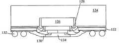
- FIG. 1shows a sectional side view of a cavity-down BGA package indicated generally by the numeral 20 .
- the cavity-down BGA package 20includes a flexible circuit tape 22 of laminated layers including a signal, trace and pad layer, referred to as a conductor layer, laminated on a polyimide tape.
- An apertureextends through the flexible circuit tape 22 and the flexible circuit tape 22 is laminated to a heat spreader 24 which includes a cavity that is aligned with the cavity of the flexible circuit tape 22 .
- a semiconductor die 26is mounted in a die-down configuration in the cavity of the heat spreader 24 and wire bonds 28 extend between the semiconductor die and wire-bonding sites of the flexible circuit tape 22 .
- the semiconductor die 26 and the wire bonds 28are encapsulated in an encapsulating material 30 which fills the cavities of the heat spreader 24 and the flexible circuit tape 22 and protrudes to cover the wire bonds 28 .
- a number of solder balls 32are attached to solder ball pads of the flexible circuit tape 22 , in the form of a ball grid array.
- the heat spreader 24provides improved heat dissipation in comparison with prior ball grid array packages.
- a cavity-down ball grid array packagehaving a flexible circuit tape including a flexible tape laminated to a conductor layer.
- the flexible circuit tapehas an aperture therein.
- a thermally conductive heat spreaderis fixed to a first surface of the flexible circuit tape and the heat spreader has a cavity aligned with the aperture of the flexible circuit tape.
- a semiconductor dieis mounted to the heat spreader in a die-down configuration in the cavity.
- a thermally conductive die adapteris fixed to the semiconductor die such that a portion of the die adapter protrudes from the cavity.
- a plurality of wire bondsconnect the semiconductor die to bond sites on the second surface of the flexible circuit tape.
- An encapsulating materialencapsulates the semiconductor die and the wire bonds and a plurality of solder balls are disposed on a second surface of the flexible circuit tape, in the form of a ball grid array.
- a method of fabricating a cavity-down ball grid array packageincludes providing a flexible circuit tape including a flexible tape laminated to a conductor layer, the flexible circuit tape having an aperture therein, fixing a thermally conductive heat spreader to a first surface of the flexible circuit tape, the heat spreader having a cavity aligned with the aperture of the flexible circuit tape.
- the methodfurther includes mounting a semiconductor die to the heat spreader in a die-down configuration in the cavity, and attaching a thermally conductive die adapter to the semiconductor die such that a portion of the die adapter protrudes from the cavity and wire bonding the semiconductor die to bond sites on the second surface of the flexible circuit tape.
- the semiconductor die and the wire bondsare encapsulated in an encapsulating material and a plurality of solder balls are fixed on a second surface of the flexible circuit tape, in the form of a ball grid array.
- a direct thermal path from the semiconductor die to the printed circuit boardis provided.
- a plurality of thermally conductive portionsare employed that together form an adapter.
- non-electrically conductive adapter portionsare employed.
- electrically conductive adapter portionsare employed and wire bonds connect the semiconductor die to portions of the die adapter, which perform as a solid power or ground.
- FIG. 1is a sectional side view of a conventional ball grid array package including a heat spreader
- FIG. 2is a sectional side view of a cavity-down ball grid array package according to an embodiment of the present invention
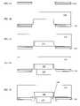
- FIGS. 3A to 3Gshow processing steps for fabricating the cavity-down ball grid array package of FIG. 2 ;
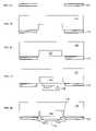
- FIGS. 4A to 4Gshow processing steps for fabricating a cavity-down ball grid array package according to another embodiment of the present invention.
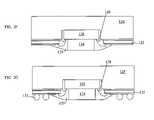
- FIG. 2there is provided a cavity-down ball grid array package 120 in accordance with an embodiment of the present invention.
- the numerals used previously in describing FIG. 1will be used again after raising the numerals by 100, where the parts to be described correspond to parts already described hereinabove.
- the package 120includes a flexible circuit tape 122 including a flexible tape laminated to a conductor layer.
- the flexible circuit tape 122has an aperture therein.
- a thermally conductive heat spreader 124is fixed to a first surface of the flexible circuit tape 122 and the heat spreader 124 has a cavity aligned with the aperture of the flexible circuit tape 122 .
- a semiconductor die 126is mounted to the heat spreader 124 in a die-down configuration in the cavity.
- a thermally conductive die adapter 134is fixed to the semiconductor die 126 such that a portion of the die adapter 134 protrudes from the cavity.
- a plurality of wire bonds 128connect the semiconductor die 126 to bond sites on the second surface of the flexible circuit tape 122 .
- An encapsulating material 130encapsulates the semiconductor die 126 and the wire bonds 128 and a plurality of solder balls 132 are disposed on a second surface of the flexible circuit tape 122 , in the form of a ball grid array.
- FIGS. 3A to 3Gshow processing steps for fabricating the cavity-down ball grid array package 120 .
- FIGS. 3A to 3Gshow processing steps for fabricating the cavity-down ball grid array package 120 .
- FIGS. 3A to 3Gshow processing steps for fabricating the cavity-down ball grid array package 120 .
- the cavity-down package 120is preferably gang fabricated and then singulated by sawing or punching, however.
- the flexible circuit tape 122includes a plurality of layers, including a signal trace and pad layer, also referred to herein as a conductor layer, laminated to a polyimide tape.
- the flexible circuit tape 122also includes a number of wire bonding sites and a number of solder ball pads.
- a solder maskcovers the flexible circuit tape 122 , with the exception of the wire bonding sites and the solder ball pads.
- the solder maskis an electrical insulator for electrically isolating the conductor layer and adhesive used in fixing the heat spreader 124 to the flexible circuit tape 122 .
- the heat spreader 124formed of thermally conductive material such as a metallic or suitable ceramic material, including a die-cavity therein, is fixed to the flexible circuit tape 122 using a tape adhesive such that the die-cavity is aligned with the aperture in the flexible circuit tape 122 ( FIG. 3B ). It will be appreciated that the heat spreader 124 is preferably in the form of a leadframe strip for the purpose of gang fabrication as indicated above.
- the semiconductor die 126is mounted in the cavity of the heat spreader 124 , in a die-down configuration, using conventional die attach technique, such as epoxy attach and curing ( FIG. 3C ).
- the thermally conductive die adapter 134is then mounted on the semiconductor die 126 such that a portion of the die adapter 134 protrudes from the cavity ( FIG. 3D ).
- Suitable die adapter materialsinclude, for example, silicon, which has similar thermo-mechanical properties to the semiconductor die and silicon coated with a vapor deposited layer of a solderable surface such as Cr, Ni and Au.
- Other die adapter materialsare also possible, including copper, alumina, and low expansion alloys such as NiFe and A42 alloys.
- Wire bonds 128are then bonded between pads of the semiconductor die 126 and the wire bonding sites of the flexible circuit tape ( FIG. 3E ).
- the wire bonds 128extend between the pads of the semiconductor die 126 in the cavity, and the flexible circuit tape 122 that is outside of the cavity.
- wire bondsare also bonded between pads of the semiconductor die 126 and the heat spreader 124 .
- the semiconductor die 126 and wire bonds 128are encapsulated in a glob-top encapsulating material 130 such that the outer surface of the die adapter 134 (the adapter surface that is opposite the surface that is attached to the semiconductor die 126 ), is exposed ( FIG. 3F ).
- the glob-top encapsulating material 130fills the cavity and is sufficient to cover the wire bonds 128 , thereby protecting the semiconductor die 126 and the wire bonds 128 , without covering the outer surface of the die adapter 134 .
- a plurality of solder balls 132are attached to the solder ball pads of the flexible circuit tape 122 to form a ball grid array ( FIG. 3G ).
- a fluxis first added to the solder ball pads on the flexible circuit tape 122 and, after placement of the solder balls 132 on the solder ball pads, the solder balls 132 are reflowed using known reflow techniques.
- the solder balls 132 on the ball padsprovide signal and power connections from the solder balls 132 , through the flexible circuit tape 122 , through the wire bonds 128 to the semiconductor die 126 .
- excess fluxis removed by cleaning with a suitable cleaner.
- the cavity-down package 120is preferably gang fabricated.
- the packageis singulated using a saw or punch technique.
- the singulated packageis ready for attachment to a printed circuit board, as shown in FIG. 2 .
- the die adapter 134is exposed for attaching to a printed circuit board when the package 120 is mounted on a printed circuit board.
- the die adapter 134provides a thermal path from the semiconductor die 126 to the printed circuit board.
- thermal vias in the printed circuit boardare utilized in dispersing heat from the package 120 .
- Suitable materials for attaching the die adapter 134 to the printed circuit boardinclude thermally conductive materials such as solder and epoxy.
- the die adapter 134is suitably sized and shaped to provide a thermal path between the semiconductor die 126 and the printed circuit board when the singulated package 120 is attached to the printed circuit board.
- FIGS. 4A to 4Gdescribe the processing steps according to an alternative embodiment of the present invention.
- FIGS. 4A to 4Care similar to FIGS. 3A to 3C and therefore need not be further described herein.
- a plurality of thermally conductive die adapter portionsare stacked together by attaching the portions together with an electrically non-conductive adhesive, to form the die adapter 134 .
- the die adapter 134includes four die adapter portions that are stacked together and are electrically isolated from each other.
- wire bonds 128are bonded between pads of the semiconductor die 126 and the wire bonding sites of the flexible circuit tape and between pads of the semiconductor die and the heat spreader 124 .
- wire bonds 128are also bonded between pads of the semiconductor die 126 and portions of the die adapter 134 , between the flexible circuit tape 122 and portions of the die adapter 134 and between portions of the die adapter 134 and the heat spreader 124 .
- Glob top encapsulation material 130is added in FIG. 4F such that the portions of the die adapter 134 are surrounded by the glob top material 130 , except the die adapter portion distal the semiconductor die 126 . The distal surface of this portion is exposed.
- FIG. 4Gis similar to FIG. 3G and therefore need not be further described herein.
- portions of the die adaptercan be employed. Portions of the die adapter can be electrically conductive or can be electrically non-conductive and the die adapter portions can be electrically isolated from each other or can be electrically connected. Portions of the die adapter of the embodiment of FIGS. 4A to 4G can perform as a solid power or a solid ground. Those skilled in the art may conceive of still other embodiments and variations, all of which are believed to be within the scope and sphere of the present invention.
Landscapes
- Engineering & Computer Science (AREA)
- Computer Hardware Design (AREA)
- Microelectronics & Electronic Packaging (AREA)
- Power Engineering (AREA)
- Physics & Mathematics (AREA)
- Condensed Matter Physics & Semiconductors (AREA)
- General Physics & Mathematics (AREA)
- Chemical & Material Sciences (AREA)
- Materials Engineering (AREA)
- Cooling Or The Like Of Semiconductors Or Solid State Devices (AREA)
Abstract
Description
Claims (9)
Priority Applications (2)
| Application Number | Priority Date | Filing Date | Title |
|---|---|---|---|
| US10/694,511US6984785B1 (en) | 2003-10-27 | 2003-10-27 | Thermally enhanced cavity-down integrated circuit package |
| US11/191,678US7342305B1 (en) | 2003-10-27 | 2005-07-28 | Thermally enhanced cavity-down integrated circuit package |
Applications Claiming Priority (1)
| Application Number | Priority Date | Filing Date | Title |
|---|---|---|---|
| US10/694,511US6984785B1 (en) | 2003-10-27 | 2003-10-27 | Thermally enhanced cavity-down integrated circuit package |
Related Child Applications (1)
| Application Number | Title | Priority Date | Filing Date |
|---|---|---|---|
| US11/191,678ContinuationUS7342305B1 (en) | 2003-10-27 | 2005-07-28 | Thermally enhanced cavity-down integrated circuit package |
Publications (1)
| Publication Number | Publication Date |
|---|---|
| US6984785B1true US6984785B1 (en) | 2006-01-10 |
Family
ID=35517796
Family Applications (2)
| Application Number | Title | Priority Date | Filing Date |
|---|---|---|---|
| US10/694,511Expired - LifetimeUS6984785B1 (en) | 2003-10-27 | 2003-10-27 | Thermally enhanced cavity-down integrated circuit package |
| US11/191,678Expired - Fee RelatedUS7342305B1 (en) | 2003-10-27 | 2005-07-28 | Thermally enhanced cavity-down integrated circuit package |
Family Applications After (1)
| Application Number | Title | Priority Date | Filing Date |
|---|---|---|---|
| US11/191,678Expired - Fee RelatedUS7342305B1 (en) | 2003-10-27 | 2005-07-28 | Thermally enhanced cavity-down integrated circuit package |
Country Status (1)
| Country | Link |
|---|---|
| US (2) | US6984785B1 (en) |
Cited By (32)
| Publication number | Priority date | Publication date | Assignee | Title |
|---|---|---|---|---|
| US20070018334A1 (en)* | 2005-07-21 | 2007-01-25 | Alain Peytavy | Security method for data protection |
| US20090236733A1 (en)* | 2008-03-18 | 2009-09-24 | Seng Guan Chow | Ball grid array package system |
| US20090283889A1 (en)* | 2008-05-16 | 2009-11-19 | Byoung Wook Jang | Integrated circuit package system |
| US20090309204A1 (en)* | 2008-06-17 | 2009-12-17 | Jong-Woo Ha | Ball grid array package stacking system |
| US20100059873A1 (en)* | 2008-09-08 | 2010-03-11 | Seng Guan Chow | Ball grid array package stacking system |
| US20100127363A1 (en)* | 2006-04-28 | 2010-05-27 | Utac Thai Limited | Very extremely thin semiconductor package |
| US7790512B1 (en) | 2007-11-06 | 2010-09-07 | Utac Thai Limited | Molded leadframe substrate semiconductor package |
| US20100311208A1 (en)* | 2008-05-22 | 2010-12-09 | Utac Thai Limited | Method and apparatus for no lead semiconductor package |
| US20100327432A1 (en)* | 2006-09-26 | 2010-12-30 | Utac Thai Limited | Package with heat transfer |
| US20110018111A1 (en)* | 2009-07-23 | 2011-01-27 | Utac Thai Limited | Leadframe feature to minimize flip-chip semiconductor die collapse during flip-chip reflow |
| US20110039371A1 (en)* | 2008-09-04 | 2011-02-17 | Utac Thai Limited | Flip chip cavity package |
| US20110133319A1 (en)* | 2009-12-04 | 2011-06-09 | Utac Thai Limited | Auxiliary leadframe member for stabilizing the bond wire process |
| US20110147931A1 (en)* | 2006-04-28 | 2011-06-23 | Utac Thai Limited | Lead frame land grid array with routing connector trace under unit |
| US20110198752A1 (en)* | 2006-04-28 | 2011-08-18 | Utac Thai Limited | Lead frame ball grid array with traces under die |
| US8013437B1 (en) | 2006-09-26 | 2011-09-06 | Utac Thai Limited | Package with heat transfer |
| US20110221051A1 (en)* | 2010-03-11 | 2011-09-15 | Utac Thai Limited | Leadframe based multi terminal ic package |
| CN101826506B (en)* | 2009-03-05 | 2011-09-21 | 南茂科技股份有限公司 | Package substrate and chip package structure |
| US20110232693A1 (en)* | 2009-03-12 | 2011-09-29 | Utac Thai Limited | Metallic solderability preservation coating on metal part of semiconductor package to prevent oxide |
| US8461694B1 (en) | 2006-04-28 | 2013-06-11 | Utac Thai Limited | Lead frame ball grid array with traces under die having interlocking features |
| US8460970B1 (en) | 2006-04-28 | 2013-06-11 | Utac Thai Limited | Lead frame ball grid array with traces under die having interlocking features |
| US8871571B2 (en) | 2010-04-02 | 2014-10-28 | Utac Thai Limited | Apparatus for and methods of attaching heat slugs to package tops |
| US9000590B2 (en) | 2012-05-10 | 2015-04-07 | Utac Thai Limited | Protruding terminals with internal routing interconnections semiconductor device |
| US9006034B1 (en) | 2012-06-11 | 2015-04-14 | Utac Thai Limited | Post-mold for semiconductor package having exposed traces |
| US9082607B1 (en) | 2006-12-14 | 2015-07-14 | Utac Thai Limited | Molded leadframe substrate semiconductor package |
| US9355940B1 (en) | 2009-12-04 | 2016-05-31 | Utac Thai Limited | Auxiliary leadframe member for stabilizing the bond wire process |
| US9449905B2 (en) | 2012-05-10 | 2016-09-20 | Utac Thai Limited | Plated terminals with routing interconnections semiconductor device |
| US9761435B1 (en) | 2006-12-14 | 2017-09-12 | Utac Thai Limited | Flip chip cavity package |
| US9805955B1 (en) | 2015-11-10 | 2017-10-31 | UTAC Headquarters Pte. Ltd. | Semiconductor package with multiple molding routing layers and a method of manufacturing the same |
| US10242953B1 (en) | 2015-05-27 | 2019-03-26 | Utac Headquarters PTE. Ltd | Semiconductor package with plated metal shielding and a method thereof |
| US10242934B1 (en) | 2014-05-07 | 2019-03-26 | Utac Headquarters Pte Ltd. | Semiconductor package with full plating on contact side surfaces and methods thereof |
| US10276477B1 (en) | 2016-05-20 | 2019-04-30 | UTAC Headquarters Pte. Ltd. | Semiconductor package with multiple stacked leadframes and a method of manufacturing the same |
| US20190355700A1 (en)* | 2016-12-28 | 2019-11-21 | Intel Corporation | Techniques for windowed substrate integrated circuit packages |
Families Citing this family (2)
| Publication number | Priority date | Publication date | Assignee | Title |
|---|---|---|---|---|
| US20120032350A1 (en)* | 2010-08-06 | 2012-02-09 | Conexant Systems, Inc. | Systems and Methods for Heat Dissipation Using Thermal Conduits |
| DE102018102144A1 (en)* | 2018-01-31 | 2019-08-01 | Tdk Electronics Ag | Electronic component |
Citations (16)
| Publication number | Priority date | Publication date | Assignee | Title |
|---|---|---|---|---|
| US5357672A (en) | 1993-08-13 | 1994-10-25 | Lsi Logic Corporation | Method and system for fabricating IC packages from laminated boards and heat spreader |
| US5578869A (en)* | 1994-03-29 | 1996-11-26 | Olin Corporation | Components for housing an integrated circuit device |
| US5659458A (en)* | 1993-06-09 | 1997-08-19 | Patchen; Lyle E. | Heat dissipative means for integrated circuit chip package |
| US5805427A (en)* | 1996-02-14 | 1998-09-08 | Olin Corporation | Ball grid array electronic package standoff design |
| US5910686A (en) | 1998-07-23 | 1999-06-08 | Vlsi Technology, Inc. | Cavity down HBGA package structure |
| US5999415A (en) | 1998-11-18 | 1999-12-07 | Vlsi Technology, Inc. | BGA package using PCB and tape in a die-down configuration |
| US6175497B1 (en) | 1998-09-30 | 2001-01-16 | World Wiser Electronics Inc. | Thermal vias-provided cavity-down IC package structure |
| US6184580B1 (en)* | 1999-09-10 | 2001-02-06 | Siliconware Precision Industries Co., Ltd. | Ball grid array package with conductive leads |
| US6266251B1 (en) | 1998-12-09 | 2001-07-24 | International Business Machines Corporation | Cavity-down ball grid array module |
| US6414849B1 (en) | 1999-10-29 | 2002-07-02 | Stmicroelectronics, Inc. | Low stress and low profile cavity down flip chip and wire bond BGA package |
| US20020096767A1 (en)* | 2001-01-25 | 2002-07-25 | Cote Kevin J. | Cavity down ball grid array package with EMI shielding and reduced thermal resistance |
| US20020109226A1 (en)* | 2001-02-15 | 2002-08-15 | Broadcom Corporation | Enhanced die-down ball grid array and method for making the same |
| US6475327B2 (en) | 2001-04-05 | 2002-11-05 | Phoenix Precision Technology Corporation | Attachment of a stiff heat spreader for fabricating a cavity down plastic chip carrier |
| US6590281B2 (en)* | 2001-11-15 | 2003-07-08 | Siliconware Precision Industries Co., Ltd. | Crack-preventive semiconductor package |
| US20030129863A1 (en)* | 2002-01-10 | 2003-07-10 | International Business Machines Corporation | Electronic package with thermally conductive standoff |
| US6713321B2 (en)* | 2000-12-01 | 2004-03-30 | Siliconware Precision Industries Co. Ltd. | Super low profile package with high efficiency of heat dissipation |
Family Cites Families (1)
| Publication number | Priority date | Publication date | Assignee | Title |
|---|---|---|---|---|
| US5339216A (en)* | 1993-03-02 | 1994-08-16 | National Semiconductor Corporation | Device and method for reducing thermal cycling in a semiconductor package |
- 2003
- 2003-10-27USUS10/694,511patent/US6984785B1/ennot_activeExpired - Lifetime
- 2005
- 2005-07-28USUS11/191,678patent/US7342305B1/ennot_activeExpired - Fee Related
Patent Citations (16)
| Publication number | Priority date | Publication date | Assignee | Title |
|---|---|---|---|---|
| US5659458A (en)* | 1993-06-09 | 1997-08-19 | Patchen; Lyle E. | Heat dissipative means for integrated circuit chip package |
| US5357672A (en) | 1993-08-13 | 1994-10-25 | Lsi Logic Corporation | Method and system for fabricating IC packages from laminated boards and heat spreader |
| US5578869A (en)* | 1994-03-29 | 1996-11-26 | Olin Corporation | Components for housing an integrated circuit device |
| US5805427A (en)* | 1996-02-14 | 1998-09-08 | Olin Corporation | Ball grid array electronic package standoff design |
| US5910686A (en) | 1998-07-23 | 1999-06-08 | Vlsi Technology, Inc. | Cavity down HBGA package structure |
| US6175497B1 (en) | 1998-09-30 | 2001-01-16 | World Wiser Electronics Inc. | Thermal vias-provided cavity-down IC package structure |
| US5999415A (en) | 1998-11-18 | 1999-12-07 | Vlsi Technology, Inc. | BGA package using PCB and tape in a die-down configuration |
| US6266251B1 (en) | 1998-12-09 | 2001-07-24 | International Business Machines Corporation | Cavity-down ball grid array module |
| US6184580B1 (en)* | 1999-09-10 | 2001-02-06 | Siliconware Precision Industries Co., Ltd. | Ball grid array package with conductive leads |
| US6414849B1 (en) | 1999-10-29 | 2002-07-02 | Stmicroelectronics, Inc. | Low stress and low profile cavity down flip chip and wire bond BGA package |
| US6713321B2 (en)* | 2000-12-01 | 2004-03-30 | Siliconware Precision Industries Co. Ltd. | Super low profile package with high efficiency of heat dissipation |
| US20020096767A1 (en)* | 2001-01-25 | 2002-07-25 | Cote Kevin J. | Cavity down ball grid array package with EMI shielding and reduced thermal resistance |
| US20020109226A1 (en)* | 2001-02-15 | 2002-08-15 | Broadcom Corporation | Enhanced die-down ball grid array and method for making the same |
| US6475327B2 (en) | 2001-04-05 | 2002-11-05 | Phoenix Precision Technology Corporation | Attachment of a stiff heat spreader for fabricating a cavity down plastic chip carrier |
| US6590281B2 (en)* | 2001-11-15 | 2003-07-08 | Siliconware Precision Industries Co., Ltd. | Crack-preventive semiconductor package |
| US20030129863A1 (en)* | 2002-01-10 | 2003-07-10 | International Business Machines Corporation | Electronic package with thermally conductive standoff |
Cited By (75)
| Publication number | Priority date | Publication date | Assignee | Title |
|---|---|---|---|---|
| US7791898B2 (en)* | 2005-07-21 | 2010-09-07 | Atmel Corporation | Security apparatus |
| US20070018334A1 (en)* | 2005-07-21 | 2007-01-25 | Alain Peytavy | Security method for data protection |
| US8492906B2 (en) | 2006-04-28 | 2013-07-23 | Utac Thai Limited | Lead frame ball grid array with traces under die |
| US8461694B1 (en) | 2006-04-28 | 2013-06-11 | Utac Thai Limited | Lead frame ball grid array with traces under die having interlocking features |
| US8575762B2 (en) | 2006-04-28 | 2013-11-05 | Utac Thai Limited | Very extremely thin semiconductor package |
| US20100127363A1 (en)* | 2006-04-28 | 2010-05-27 | Utac Thai Limited | Very extremely thin semiconductor package |
| US8685794B2 (en) | 2006-04-28 | 2014-04-01 | Utac Thai Limited | Lead frame land grid array with routing connector trace under unit |
| US8704381B2 (en) | 2006-04-28 | 2014-04-22 | Utac Thai Limited | Very extremely thin semiconductor package |
| US20110198752A1 (en)* | 2006-04-28 | 2011-08-18 | Utac Thai Limited | Lead frame ball grid array with traces under die |
| US20110147931A1 (en)* | 2006-04-28 | 2011-06-23 | Utac Thai Limited | Lead frame land grid array with routing connector trace under unit |
| US8487451B2 (en) | 2006-04-28 | 2013-07-16 | Utac Thai Limited | Lead frame land grid array with routing connector trace under unit |
| US8460970B1 (en) | 2006-04-28 | 2013-06-11 | Utac Thai Limited | Lead frame ball grid array with traces under die having interlocking features |
| US8652879B2 (en) | 2006-04-28 | 2014-02-18 | Utac Thai Limited | Lead frame ball grid array with traces under die |
| US9099317B2 (en) | 2006-04-28 | 2015-08-04 | Utac Thai Limited | Method for forming lead frame land grid array |
| US8310060B1 (en) | 2006-04-28 | 2012-11-13 | Utac Thai Limited | Lead frame land grid array |
| US20100327432A1 (en)* | 2006-09-26 | 2010-12-30 | Utac Thai Limited | Package with heat transfer |
| US8125077B2 (en) | 2006-09-26 | 2012-02-28 | Utac Thai Limited | Package with heat transfer |
| US8013437B1 (en) | 2006-09-26 | 2011-09-06 | Utac Thai Limited | Package with heat transfer |
| US9711343B1 (en) | 2006-12-14 | 2017-07-18 | Utac Thai Limited | Molded leadframe substrate semiconductor package |
| US9099294B1 (en) | 2006-12-14 | 2015-08-04 | Utac Thai Limited | Molded leadframe substrate semiconductor package |
| US9082607B1 (en) | 2006-12-14 | 2015-07-14 | Utac Thai Limited | Molded leadframe substrate semiconductor package |
| US9093486B2 (en) | 2006-12-14 | 2015-07-28 | Utac Thai Limited | Molded leadframe substrate semiconductor package |
| US9196470B1 (en) | 2006-12-14 | 2015-11-24 | Utac Thai Limited | Molded leadframe substrate semiconductor package |
| US9899208B2 (en) | 2006-12-14 | 2018-02-20 | Utac Thai Limited | Molded leadframe substrate semiconductor package |
| US9761435B1 (en) | 2006-12-14 | 2017-09-12 | Utac Thai Limited | Flip chip cavity package |
| US7790512B1 (en) | 2007-11-06 | 2010-09-07 | Utac Thai Limited | Molded leadframe substrate semiconductor package |
| US8338922B1 (en) | 2007-11-06 | 2012-12-25 | Utac Thai Limited | Molded leadframe substrate semiconductor package |
| US7863732B2 (en) | 2008-03-18 | 2011-01-04 | Stats Chippac Ltd. | Ball grid array package system |
| US20090236733A1 (en)* | 2008-03-18 | 2009-09-24 | Seng Guan Chow | Ball grid array package system |
| US20090283889A1 (en)* | 2008-05-16 | 2009-11-19 | Byoung Wook Jang | Integrated circuit package system |
| US20100311208A1 (en)* | 2008-05-22 | 2010-12-09 | Utac Thai Limited | Method and apparatus for no lead semiconductor package |
| US8063470B1 (en) | 2008-05-22 | 2011-11-22 | Utac Thai Limited | Method and apparatus for no lead semiconductor package |
| US8071426B2 (en) | 2008-05-22 | 2011-12-06 | Utac Thai Limited | Method and apparatus for no lead semiconductor package |
| US20090309204A1 (en)* | 2008-06-17 | 2009-12-17 | Jong-Woo Ha | Ball grid array package stacking system |
| US8039942B2 (en) | 2008-06-17 | 2011-10-18 | Stats Chippac Ltd. | Ball grid array package stacking system |
| US8143104B2 (en) | 2008-06-17 | 2012-03-27 | Stats Chippac Ltd. | Method for manufacturing ball grid array package stacking system |
| US9947605B2 (en) | 2008-09-04 | 2018-04-17 | UTAC Headquarters Pte. Ltd. | Flip chip cavity package |
| US20110039371A1 (en)* | 2008-09-04 | 2011-02-17 | Utac Thai Limited | Flip chip cavity package |
| US20100059873A1 (en)* | 2008-09-08 | 2010-03-11 | Seng Guan Chow | Ball grid array package stacking system |
| US7871862B2 (en) | 2008-09-08 | 2011-01-18 | Stats Chippac Ltd. | Ball grid array package stacking system |
| CN101826506B (en)* | 2009-03-05 | 2011-09-21 | 南茂科技股份有限公司 | Package substrate and chip package structure |
| US8569877B2 (en) | 2009-03-12 | 2013-10-29 | Utac Thai Limited | Metallic solderability preservation coating on metal part of semiconductor package to prevent oxide |
| US8431443B2 (en) | 2009-03-12 | 2013-04-30 | Utac Thai Limited | Metallic solderability preservation coating on metal part of semiconductor package to prevent oxide |
| US20110232693A1 (en)* | 2009-03-12 | 2011-09-29 | Utac Thai Limited | Metallic solderability preservation coating on metal part of semiconductor package to prevent oxide |
| US8367476B2 (en) | 2009-03-12 | 2013-02-05 | Utac Thai Limited | Metallic solderability preservation coating on metal part of semiconductor package to prevent oxide |
| US20110018111A1 (en)* | 2009-07-23 | 2011-01-27 | Utac Thai Limited | Leadframe feature to minimize flip-chip semiconductor die collapse during flip-chip reflow |
| US9449900B2 (en) | 2009-07-23 | 2016-09-20 | UTAC Headquarters Pte. Ltd. | Leadframe feature to minimize flip-chip semiconductor die collapse during flip-chip reflow |
| US20110133319A1 (en)* | 2009-12-04 | 2011-06-09 | Utac Thai Limited | Auxiliary leadframe member for stabilizing the bond wire process |
| US9355940B1 (en) | 2009-12-04 | 2016-05-31 | Utac Thai Limited | Auxiliary leadframe member for stabilizing the bond wire process |
| US8368189B2 (en) | 2009-12-04 | 2013-02-05 | Utac Thai Limited | Auxiliary leadframe member for stabilizing the bond wire process |
| US8575732B2 (en) | 2010-03-11 | 2013-11-05 | Utac Thai Limited | Leadframe based multi terminal IC package |
| US20110221051A1 (en)* | 2010-03-11 | 2011-09-15 | Utac Thai Limited | Leadframe based multi terminal ic package |
| US8722461B2 (en) | 2010-03-11 | 2014-05-13 | Utac Thai Limited | Leadframe based multi terminal IC package |
| US8871571B2 (en) | 2010-04-02 | 2014-10-28 | Utac Thai Limited | Apparatus for and methods of attaching heat slugs to package tops |
| US9000590B2 (en) | 2012-05-10 | 2015-04-07 | Utac Thai Limited | Protruding terminals with internal routing interconnections semiconductor device |
| US9029198B2 (en) | 2012-05-10 | 2015-05-12 | Utac Thai Limited | Methods of manufacturing semiconductor devices including terminals with internal routing interconnections |
| US9449905B2 (en) | 2012-05-10 | 2016-09-20 | Utac Thai Limited | Plated terminals with routing interconnections semiconductor device |
| US9972563B2 (en) | 2012-05-10 | 2018-05-15 | UTAC Headquarters Pte. Ltd. | Plated terminals with routing interconnections semiconductor device |
| US9922914B2 (en) | 2012-05-10 | 2018-03-20 | Utac Thai Limited | Plated terminals with routing interconnections semiconductor device |
| US9922913B2 (en) | 2012-05-10 | 2018-03-20 | Utac Thai Limited | Plated terminals with routing interconnections semiconductor device |
| US9397031B2 (en) | 2012-06-11 | 2016-07-19 | Utac Thai Limited | Post-mold for semiconductor package having exposed traces |
| US9006034B1 (en) | 2012-06-11 | 2015-04-14 | Utac Thai Limited | Post-mold for semiconductor package having exposed traces |
| US10242934B1 (en) | 2014-05-07 | 2019-03-26 | Utac Headquarters Pte Ltd. | Semiconductor package with full plating on contact side surfaces and methods thereof |
| US10269686B1 (en) | 2015-05-27 | 2019-04-23 | UTAC Headquarters PTE, LTD. | Method of improving adhesion between molding compounds and an apparatus thereof |
| US10242953B1 (en) | 2015-05-27 | 2019-03-26 | Utac Headquarters PTE. Ltd | Semiconductor package with plated metal shielding and a method thereof |
| US9922843B1 (en) | 2015-11-10 | 2018-03-20 | UTAC Headquarters Pte. Ltd. | Semiconductor package with multiple molding routing layers and a method of manufacturing the same |
| US10096490B2 (en) | 2015-11-10 | 2018-10-09 | UTAC Headquarters Pte. Ltd. | Semiconductor package with multiple molding routing layers and a method of manufacturing the same |
| US10163658B2 (en) | 2015-11-10 | 2018-12-25 | UTAC Headquarters PTE, LTD. | Semiconductor package with multiple molding routing layers and a method of manufacturing the same |
| US10032645B1 (en) | 2015-11-10 | 2018-07-24 | UTAC Headquarters Pte. Ltd. | Semiconductor package with multiple molding routing layers and a method of manufacturing the same |
| US9917038B1 (en) | 2015-11-10 | 2018-03-13 | Utac Headquarters Pte Ltd | Semiconductor package with multiple molding routing layers and a method of manufacturing the same |
| US9805955B1 (en) | 2015-11-10 | 2017-10-31 | UTAC Headquarters Pte. Ltd. | Semiconductor package with multiple molding routing layers and a method of manufacturing the same |
| US10325782B2 (en) | 2015-11-10 | 2019-06-18 | UTAC Headquarters Pte. Ltd. | Semiconductor package with multiple molding routing layers and a method of manufacturing the same |
| US10734247B2 (en) | 2015-11-10 | 2020-08-04 | Utac Headquarters PTE. Ltd | Semiconductor package with multiple molding routing layers and a method of manufacturing the same |
| US10276477B1 (en) | 2016-05-20 | 2019-04-30 | UTAC Headquarters Pte. Ltd. | Semiconductor package with multiple stacked leadframes and a method of manufacturing the same |
| US20190355700A1 (en)* | 2016-12-28 | 2019-11-21 | Intel Corporation | Techniques for windowed substrate integrated circuit packages |
Also Published As
| Publication number | Publication date |
|---|---|
| US7342305B1 (en) | 2008-03-11 |
Similar Documents
| Publication | Publication Date | Title |
|---|---|---|
| US6984785B1 (en) | Thermally enhanced cavity-down integrated circuit package | |
| US6781242B1 (en) | Thin ball grid array package | |
| US7402906B2 (en) | Enhanced die-down ball grid array and method for making the same | |
| US6800948B1 (en) | Ball grid array package | |
| US6818978B1 (en) | Ball grid array package with shielding | |
| US7102225B2 (en) | Die-up ball grid array package with printed circuit board attachable heat spreader | |
| US7372151B1 (en) | Ball grid array package and process for manufacturing same | |
| US6323066B2 (en) | Heat-dissipating structure for integrated circuit package | |
| US6359341B1 (en) | Ball grid array integrated circuit package structure | |
| US7259457B2 (en) | Die-up ball grid array package including a substrate capable of mounting an integrated circuit die and method for making the same | |
| US7312108B2 (en) | Method for assembling a ball grid array package with two substrates | |
| US7132744B2 (en) | Enhanced die-up ball grid array packages and method for making the same | |
| US6856013B1 (en) | Integrated circuit packages, ball-grid array integrated circuit packages and methods of packaging an integrated circuit | |
| US6627990B1 (en) | Thermally enhanced stacked die package | |
| WO2004070790A2 (en) | Molded high density electronic packaging structure for high performance applications | |
| US20030064542A1 (en) | Methods of packaging an integrated circuit |
Legal Events
| Date | Code | Title | Description |
|---|---|---|---|
| AS | Assignment | Owner name:ASAT LTD., HONG KONG Free format text:ASSIGNMENT OF ASSIGNORS INTEREST;ASSIGNORS:DIAO, QUZHONG;MCLELLAN, NEIL;KIRLOSKAR, MOHAN;REEL/FRAME:014364/0285;SIGNING DATES FROM 20031211 TO 20031230 | |
| STCF | Information on status: patent grant | Free format text:PATENTED CASE | |
| FPAY | Fee payment | Year of fee payment:4 | |
| FEPP | Fee payment procedure | Free format text:PAYOR NUMBER ASSIGNED (ORIGINAL EVENT CODE: ASPN); ENTITY STATUS OF PATENT OWNER: LARGE ENTITY Free format text:PAYER NUMBER DE-ASSIGNED (ORIGINAL EVENT CODE: RMPN); ENTITY STATUS OF PATENT OWNER: LARGE ENTITY | |
| AS | Assignment | Owner name:JPMORGAN CHASE BANK, N.A., AS COLLATERAL AGENT,TEX Free format text:GRANT OF SECURITY INTEREST IN PATENT RIGHTS - FIRST PRIORITY;ASSIGNOR:UTAC HONG KONG LIMITED;REEL/FRAME:024599/0743 Effective date:20100604 Owner name:JPMORGAN CHASE BANK, N.A., AS COLLATERAL AGENT,TEX Free format text:GRANT OF SECURITY INTEREST IN PATENT RIGHTS - SECOND PRIORITY;ASSIGNOR:UTAC HONG KONG LIMITED;REEL/FRAME:024599/0827 Effective date:20100604 Owner name:THE HONGKONG AND SHANGHAI BANKING CORPORATION LIMI Free format text:GRANT OF SECURITY INTEREST IN PATENT RIGHTS - SECOND PRIORITY;ASSIGNOR:UTAC HONG KONG LIMITED;REEL/FRAME:024611/0097 Effective date:20100604 Owner name:JPMORGAN CHASE BANK, N.A., AS COLLATERAL AGENT, TE Free format text:GRANT OF SECURITY INTEREST IN PATENT RIGHTS - FIRST PRIORITY;ASSIGNOR:UTAC HONG KONG LIMITED;REEL/FRAME:024599/0743 Effective date:20100604 Owner name:JPMORGAN CHASE BANK, N.A., AS COLLATERAL AGENT, TE Free format text:GRANT OF SECURITY INTEREST IN PATENT RIGHTS - SECOND PRIORITY;ASSIGNOR:UTAC HONG KONG LIMITED;REEL/FRAME:024599/0827 Effective date:20100604 | |
| AS | Assignment | Owner name:UTAC HONG KONG LIMITED, HONG KONG Free format text:CHANGE OF NAME;ASSIGNOR:ASAT LIMITED;REEL/FRAME:025217/0342 Effective date:20100325 | |
| FPAY | Fee payment | Year of fee payment:8 | |
| AS | Assignment | Owner name:UTAC HEADQUARTERS PTE. LTD., SINGAPORE Free format text:ASSIGNMENT OF ASSIGNORS INTEREST;ASSIGNOR:UTAC HONG KONG LIMITED;REEL/FRAME:037880/0534 Effective date:20150508 | |
| AS | Assignment | Owner name:UTAC HEADQUARTERS PTE. LTD., SINGAPORE Free format text:CORRECTIVE ASSIGNMENT TO CORRECT THE ADD ANNEX INADVERTENTLY LEFT OUT ORIGINAL ASSIGNMENT DOCUMENT PREVIOUSLY RECORDED AT REEL: 037880 FRAME: 0534. ASSIGNOR(S) HEREBY CONFIRMS THE ASSIGNMENT;ASSIGNOR:UTAC HONG KONG LIMITED;REEL/FRAME:039822/0591 Effective date:20150508 | |
| FPAY | Fee payment | Year of fee payment:12 |