US6983342B2 - High speed OC-768 configurable link layer chip - Google Patents
High speed OC-768 configurable link layer chipDownload PDFInfo
- Publication number
- US6983342B2 US6983342B2US10/266,232US26623202AUS6983342B2US 6983342 B2US6983342 B2US 6983342B2US 26623202 AUS26623202 AUS 26623202AUS 6983342 B2US6983342 B2US 6983342B2
- Authority
- US
- United States
- Prior art keywords
- link layer
- controllers
- integrated circuit
- protocol
- serializer
- Prior art date
- Legal status (The legal status is an assumption and is not a legal conclusion. Google has not performed a legal analysis and makes no representation as to the accuracy of the status listed.)
- Expired - Lifetime, expires
Links
- 230000003287optical effectEffects0.000claimsdescription16
- 230000008878couplingEffects0.000claimsdescription7
- 238000010168coupling processMethods0.000claimsdescription7
- 238000005859coupling reactionMethods0.000claimsdescription7
- 238000004519manufacturing processMethods0.000claimsdescription3
- 238000000034methodMethods0.000claims9
- 238000010586diagramMethods0.000description17
- 230000001419dependent effectEffects0.000description7
- 230000006870functionEffects0.000description6
- 238000001914filtrationMethods0.000description3
- 239000002184metalSubstances0.000description2
- 239000004606Fillers/ExtendersSubstances0.000description1
- 238000003491arrayMethods0.000description1
- 238000001514detection methodMethods0.000description1
- 238000009792diffusion processMethods0.000description1
- 239000003292glueSubstances0.000description1
- 230000003993interactionEffects0.000description1
- 238000002826magnetic-activated cell sortingMethods0.000description1
- 230000001360synchronised effectEffects0.000description1
Images


Classifications
- H—ELECTRICITY
- H04—ELECTRIC COMMUNICATION TECHNIQUE
- H04L—TRANSMISSION OF DIGITAL INFORMATION, e.g. TELEGRAPHIC COMMUNICATION
- H04L69/00—Network arrangements, protocols or services independent of the application payload and not provided for in the other groups of this subclass
- H04L69/30—Definitions, standards or architectural aspects of layered protocol stacks
- H04L69/32—Architecture of open systems interconnection [OSI] 7-layer type protocol stacks, e.g. the interfaces between the data link level and the physical level
- H04L69/322—Intralayer communication protocols among peer entities or protocol data unit [PDU] definitions
- H04L69/324—Intralayer communication protocols among peer entities or protocol data unit [PDU] definitions in the data link layer [OSI layer 2], e.g. HDLC
- H—ELECTRICITY
- H04—ELECTRIC COMMUNICATION TECHNIQUE
- H04L—TRANSMISSION OF DIGITAL INFORMATION, e.g. TELEGRAPHIC COMMUNICATION
- H04L69/00—Network arrangements, protocols or services independent of the application payload and not provided for in the other groups of this subclass
- H04L69/30—Definitions, standards or architectural aspects of layered protocol stacks
- H04L69/32—Architecture of open systems interconnection [OSI] 7-layer type protocol stacks, e.g. the interfaces between the data link level and the physical level
Definitions
- the present inventionrelates to network chip architecture generally and, more particularly, to a high speed OC-768 configurable link layer chip.
- Each channel of a conventional customer configurable network interfaceutilizes large field programmable gate arrays (FPGAs) for the media access controller (MAC) layer and glue, application specific integrated circuits (ASICs) or FPGAs for the forward error correction (FEC) layer and standard products for the serializer/de-serializer (SERDES).
- FPGAsfield programmable gate arrays
- ASICsapplication specific integrated circuits
- FECforward error correction
- SERDESserializer/de-serializer
- OC-768 deviceswill be fielded in wide area network (WAN), storage area network (SAN), and local area network (LAN) applications.
- WANwide area network
- SANstorage area network
- LANlocal area network
- a fast time to marketis desirable in all the applications.
- each applicationcan have slightly different configurations.
- each optical customercan utilize a proprietary forward error correction (FEC) algorithm
- FECforward error correction
- the present inventionconcerns an integrated circuit comprising a plurality of link layer controllers.
- the plurality of link layer controllersmay be configured to operate independently in a first mode and cooperatively in a second mode.
- the objects, features and advantages of the present inventioninclude providing a high speed OC-768 configurable link layer chip that may (i) have a reasonable power budget, (ii) be implemented in a single package, (iii) provide an integrated design, (iv) provide a single base architecture that satisfies multiple markets, (v) provide a single base architecture that satisfies multiple slightly different applications of a single customer, (vi) reduce engineering costs, (vii) provide easier parts management and/or (viii) provide a solution where the customer designs only the customer value added areas.
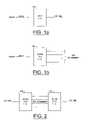
- FIGS. 1A and 1Bare block diagrams of example configurations of a preferred embodiment of the present invention.
- FIG. 2is a block diagram of an example application in accordance with a preferred embodiment of the present invention.
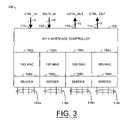
- FIG. 3is a block diagram of a preferred embodiment of the present invention.
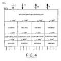
- FIG. 4is a detailed block diagram of another preferred embodiment of the present invention.
- FIG. 5is a block diagram of yet another preferred embodiment of the present invention.
- FIG. 6is a more detailed block diagram of an example application of the embodiment of FIG. 5 ;
- FIG. 7is a more detailed block of an example implementation of the embodiment of FIG. 5 ;
- FIG. 8is a block diagram of various example channel implementation in accordance with the present invention.
- FIG. 9is a block diagram of an implementation of the embodiment of FIG. 1A ;
- FIG. 10is an alternative embodiment of the embodiment of FIG. 1A .
- FIGS. 1A and 1Bblock diagrams of a circuit 100 are shown in accordance with a preferred embodiment of the present invention.
- the circuit 100may be implemented, in one example, as a link layer chip.
- the circuit 100may be configured, in a first mode, as a 40 Gb/s device ( FIG. 1A ) that may run as, in one example, an OC-768 compliant link layer chip and, in a second mode, as a quad 10 Gb/s device ( FIG. 1B ).
- the circuit 100may be rapidly customized to support different applications in storage area networks (SAN), wide area networks (WAN) and/or large area networks (LAN).
- SANstorage area networks
- WANwide area networks
- LANlarge area networks
- the circuit 100may be configured to support a number of communication protocols (e.g., WIS, SPI-5, SPI-4, XGMII, XAUI, etc.).
- the circuit 100may provide user customizable logic areas that may be configured to provide a number of custom (or proprietary) functions (e.g., forward error correcting (FEC), packet filtering, host interface bus protocol management, etc.).
- FECforward error correcting
- the circuit 100may be implemented as a single integrated circuit.
- the circuit 100is generally configured to couple a host device (or system) to a synchronous optical network (SONET). In one example, the circuit 100 may be configured to provide an OC-768 compliant interface.
- SONETsynchronous optical network
- a number of circuits 100may be coupled together to provide a link in a high speed optical network (e.g., OC-768) via a number of lower speed links (e.g., 10 Gb/s Ethernet).
- the circuits 100may be configured to distribute data from the high speed network on the number of lower speed links and recombine the data from the lower speed links for presentation to the high speed network.
- the circuit 100may comprise a circuit 102 , a number of circuits 104 a–n and a number of circuits 106 a–n .
- the circuit 102may be implemented as an interface controller.
- the circuits 104 a–nmay be implemented as link layer controllers.
- the circuits 106 a–nmay be implemented as serializer/deserializer (SERDES) circuits.
- SERDESserializer/deserializer
- the circuit 102may be configured to implement one or more communication protocols (e.g., SPI-4, SPI-5, etc.).
- the circuit 102may have an input 110 that may receive one or more control signals (e.g., CTRL — IN), an input 112 that may receive one or more data signals (e.g., DATA — IN), an output 114 that may present one or more data signals (e.g., DATA — OUT) and an output 116 that may present one or more control signals (e.g., CTRL — OUT).
- the interface controller 102is generally coupled to the circuits 104 a–n .
- the circuit 102may be configured to operate the circuits 104 a–n cooperatively as a single high speed communication channel, in a first mode, and independently as a plurality of lower-speed communication channels, in a second mode.
- the circuits 104 a–nmay be implemented, in one example, as media access controllers (MACs). Alternatively, the circuits 104 a – 104 n may be implemented as framers. However, other types and/or combinations of link layer controllers may be implemented accordingly to meet the design criteria of a particular application.
- Each of the circuits 104 a–nis generally coupled between the circuit 102 and a respective one of the circuits 106 a–n .
- the couplings (or interfaces) between the circuits 104 a–n and the circuits 102 and 106 a–nare generally customizable (or configurable) to meet the design criteria of a particular application.
- the circuits 106 a–nmay be implemented, in one example, as serializer/deserializer (SERDES) circuits. Each of the circuits 106 a–n generally has a respective input/output interface 118 a–n .
- the circuits 106 a–nmay be configured to support one or more communication protocols (e.g., WIS, SPI-5, SPI-4, XGMII, XAUI, etc.).
- the circuit 100 ′may comprise an interface controller 102 ′, a number of link layer controllers 104 a ′– 104 n ′, and a number of SERDES 106 a ′– 106 n .
- the circuit 100 ′may be implemented similarly to the circuit 100 except that each of the link layer controllers 104 a ′– 104 n ′ may be coupled to the respective serializer/deserializer 106 a ′– 106 n ′ via a respective customizable logic block 120 a–n .
- the customizable logic blocks 120 a–nmay be configured, in one example, to provide proprietary (user specific) interface circuitry (e.g., forward error correction (FEC), packet filtering, etc.).
- the customizable logic blocks 120 a–nmay be implemented with one or more diffusion layers that may comprise structures (e.g., A-cells, standard cells, hard macros, sea-of-gates, gate array, etc.) that may form transistors, logic, memory and/or other custom circuitry with the addition of one or more metal layers (e.g., wiring, routing, etc.).
- the customizing metal layersmay be deposited at a different time (e.g., subsequent manufacturing step) than the fabrication of the circuit 100 ′.
- the circuit 100 ′may be fabricated and stored for customization at a later date.
- FIG. 5a block diagram of a circuit 100 ′′ is shown illustrating yet another preferred embodiment of the present invention.
- the circuit 100 ′′may comprise a circuit 102 ′′, a number of circuits 104 a ′′– 104 n ′′, a number of circuits 106 a ′′– 106 n ′′, a number of customizable logic blocks 120 a ′– 120 n ′ and a user customizable logic block 122 .
- the circuit 100 ′′be implemented similarly to the circuit 100 ′ of FIG. 4 except that the user customizable logic block 122 may couple the circuit 102 ′′ and the circuits 104 a ′′– 104 n ′′.
- the customizable logic blocks 120 a ′– 120 n ′ and 122may be implemented similarly to the blocks 120 a–n (described above in connection with FIG. 3 ).
- the user customizable logic blocks 120 a ′– 120 n ′ and 122may comprise gates, memory, etc. that may allow for flexible designs such as statistic gathering for the link layer controllers 104 a ′′– 104 n ′′.
- the customizable logic blocks 120 a ′– 120 n ′ and 122provide for user definable customization of the interactions between the circuits 102 ′′, 104 ′′– 104 n ′′ and 106 a ′′– 106 n ′′ to meet the design criteria of particular applications.
- the customizable block 122may provide a number of user definable input/outputs 124 .
- the present inventionmay define a set of input/outputs, memory and logic that provides standard options of a link layer chip design while leaving room for customization to include user specific elements, features and/or functions. For example, customized (or proprietary) error detection, tracking and/or correction may be implemented via the customizable logic blocks 120 a ′– 120 n ′ and 122 .
- the circuit 102 ′′may comprise a control pin logic and I/O block 130 , a number of banks of quad serializer/deserializers 132 , a configurable multiplexer circuit 134 that may be configured to select between a number of protocols (e.g., SPI-5, SPI-4, link layers using SPI-5 narrow mode, etc.), an SPI-5 link layer controller 136 and a number of (e.g., four) SPI-4 link layer controllers 138 .
- protocolse.g., SPI-5, SPI-4, link layers using SPI-5 narrow mode, etc.
- the circuit 100 ′′may comprise a double data rate control circuit 140 that may provide one or more interfaces 142 to, for example, one or more double data rate (DDR) random access memory (RAM) interfaces, a processor interface and/or one or more general purpose input/outputs or interfaces (not shown).
- Each of the circuits 104 a ′′– 104 n ′′may comprise, in one example, a FIFO, a FIFO manager, flow control logic, a media access controller and a memory and statistics support.
- the circuit 100 ′′may further comprise a number of (e.g., four) SFI-4 controllers 144 , a number of FIFOs 146 , a number of controllers (e.g., XAUI/XGXS) 148 , and a configurable multiplexer circuit 150 that may be configured to select between, for example, an SFI-4, a XAUI and/or a SFI-5 mode.
- the circuits 106 a ′′– 106 n ′′may be implemented, in one example, as quad 3.125 GB/s SERDES circuits.
- circuits 134 , 136 , 138 and 140may be implemented in the customizable logic block 122 and the circuits 144 , 146 , 148 and 150 may be implemented via the customizable logic blocks 120 a ′′– 120 n′′.
- the interface controller 102 ′′may be configured to couple the circuit 100 ′′ to an application specific integrated circuit (ASIC), traffic manager or network processor (NP) chip 152 .
- the customizable logic block 122may be configured to provide control of the MACS 104 a ′′– 104 n ′′ and the logic blocks 120 a ′′– 120 n ′′ may be configured to provide a reconciliation function between the respective MACs 104 a ′′– 104 n ′′ and the respective serializer/deserializers 106 a ′′– 106 n ′′.
- Each of the serializer/deserializers 106 a ′′– 106 n ′′may be configured to support an interface protocol (e.g., XAUI, etc.) for communicating with a respective media dependent interface (MDI) 154 a – 154 n.
- an interface protocole.g., XAUI, etc.
- MDImedia dependent interface
- each of the MDIs 154 a – 154 nmay be implemented as an electrical-to-optical interface (e.g., a XENPAK compliant 10 Gb/s Ethernet (10 GbE) transceiver).
- the circuits 154 a – 154 nmay be implemented as optical modules incorporating a complete transmit and receive physical layer functionality from a 10 Gb/s optical interface to an XAUI (e.g., four channels X 3.125 Gb/s electrical interface).
- the circuits 154 a – 154 nmay be further configured to provide 8B/10B and/or 64B/66B coding and a MDIO control interface.
- the serializer/deserializers 106 a ′′– 106 n ′′may be configured to support one or more different bus protocols (e.g., XAUI, SPI-5, etc.).
- the serializer/deserializer 106 a ′′– 106 n ′′may be implemented with ethernet (e.g., GigaBlaze) and/or optical (e.g., HyperPHY) cores (GigaBlaze and HyperPHY are trademarks of LSI Logic Corp., Milpitas, Calif.).
- ethernete.g., GigaBlaze
- opticale.g., HyperPHY cores
- the present inventionmay reduce the number of pins used for coupling the traffic manager and MAC chips.
- a reference ethernet implementationmay include a number of functions and protocols (e.g., column 160 ).
- a link layer controllermay communicate with higher layers using the SPI-4 P2 protocol or some other protocol.
- a reconciliation layermay communicate with a subsequent layer (or device) via a 10 GB/s medium independent interface (XGMII) protocol.
- XGMIImedium independent interface
- optional 10 GB/s extender sublayersmay be implemented to convert the short run XGMII protocol to a long run 10 GB/s attachment unit interface (XAUI) protocol and back again.
- An encoding/decoding/error correcting layermay include a physical coding sublayer (PCS), a physical medium attachment (PMA) and support for the XGMII protocol, as well as SFI-4 and XSBI protocols.
- the encoding/decoding/error correcting layermay communicate with a physical medium dependent interface (PMD) layer that provides the physical network connection via a medium dependent interface (MDI) protocol.
- PMDphysical medium dependent interface
- the higher layers of an ethernet implementationmay be provided with an application specific integrated circuit (ASIC), a traffic manager or an NP chip that may be interfaced with the present invention.
- ASICapplication specific integrated circuit
- the present inventionmay provide a flexible platform that generally supports implementing various ethernet layers that communicate with the higher layers via the link layer in a number of ways.
- the present inventionmay provide, for example, a cost effective building block for implementing high speed (e.g., 40 GB/s) optical networks.
- the reconciliation layer 164may communicate with a 10 GB/s serializer/deserializer 166 via the XGMII protocol.
- the serializer/deserializer 166may communicate with the physical layer via an optical interface 168 .
- the serializer/deserializer 166may be configured to manage the error correction operations and physical medium attachment functions.
- the reconciliation layer 164may communicate with a serializer/deserializer 172 via an XMGII protocol.
- the serializer/deserializer 172may be configured to communicate via an XAUI protocol with, for example, an optical interface 174 (e.g., in a 10G Ethernet Forum 10GBASE-X channel) or an electrical-to-optical interface 176 (e.g., in a 10G Ethernet Forum 10GBASE-R channel).
- the interfaces 174 and 176may be configured to provide the error correction, physical medium attachment and physical medium dependent interface functions.
- an alternative 10G Ethernet Forum 10GBASE-R implementationmay comprise a LAN PHY chip (or core) 182 configured to couple (i) to the higher layers via an SPI-4 P2 or other interface and (ii) to a serializer/deserializer 184 via an SFI-4 or XSBI interface.
- the serializer/deserializer 184may provide the physical medium attachment interface for coupling to an optical interface 186 .
- the optical interface 186generally provides the physical medium dependent interface.
- a 10G Ethernet Forum 10GBASE-W implementationmay comprise a serializer/deserializer 192 , a serializer/deserializer 194 , a physical coding sublayer (PCS) 196 , a single universal physical medium dependent (PMD) interface (SUPI) 198 and an optical link 200 .
- the serializer/deserializer 192may connect (i) to the reconciliation layer 164 via the XGMII protocol and (ii) to the serializer/deserializer 194 via an XAUI protocol.
- the serializer/deserializer 194may connect to the PCS 196 via the XGMII protocol.
- the PCS 196may connect to the SUPI 198 via an SFI-4 or XSBI protocol.
- the SUPI 198may provide the interface to the optical link to the physical layer.
- an alternative implementation of the 10G Ethernet Forum 10GBASE-W channelmay comprise a WAN MAC/PHY chip 212 coupled between the higher layers and a SUPI 214 .
- the SUPI 214may be configured to couple the channel to the physical layer via an optical link 216 .
- the present inventionmay be configured to implement a 40 GB/s SPI-5 link layer.
- the link layermay be implemented in an ASIC or traffic manager/NP chip 220 .
- the circuit 100may be configured to provide a framer 222 , a forward error correction (FEC) block 224 , and a 40 GB/s serializer/deserializer (SERDES) 226 .
- the framer 222may be implemented in (i) dedicated logic, (ii) customizable user defined logic, or (iii) a combination of dedicated and custom logic.
- the FEC 224may be implemented in customizable user defined logic (e.g., the custom logic described in connection with FIGS. 3–5 above).
- the framer 222may be coupled (i) to the ASIC 220 via an SPI-5 protocol and (ii) to the FEC 224 via an SFI-5 protocol.
- the FEC 224may be coupled to the SERDES 226 via an SFI-5 protocol.
- the SERDES 226may be configured to couple the implementation to the physical layer via a laser/optical physical medium dependent interface 228 .
- the circuit 100 ′′(described in more detail in connection with FIGS. 5 and 6 above) may be configured as a 40 GB/s SPI-5 implementation.
- the circuit 100 ′′may be coupled via an SPI-5 interface to an ASIC or traffic manager/NP chip that may be configured to implement higher network layers of, for example, an OC-768 compliant network.
- the circuit 100 ′′may be configured to provide a number of MAC control blocks 230 , a number of MACs 104 a ′′– 104 n ′′, a number of reconciliation blocks 232 a – 232 n , the framer block 222 , the FEC block 224 , and a number of SERDES 106 a ′′– 106 n ′′.
- the reconciliation blocks 232 a – 232 n , the framer 222 , and the FEC block 224may be implemented in the custom logic blocks 120 a ′– 120 n ′.
- the MAC control blocks 230 a – 230 nmay be implemented in the custom logic 122 . However other configurations and resource assignments may be implemented to meet the design criteria of a particular application.
- the circuit 100 ′′may be coupled to the 40 GB/s SERDES 226 via an SFI-5 interface.
Landscapes
- Engineering & Computer Science (AREA)
- Computer Security & Cryptography (AREA)
- Computer Networks & Wireless Communication (AREA)
- Signal Processing (AREA)
- Design And Manufacture Of Integrated Circuits (AREA)
- Information Transfer Systems (AREA)
Abstract
Description
Claims (21)
Priority Applications (1)
| Application Number | Priority Date | Filing Date | Title |
|---|---|---|---|
| US10/266,232US6983342B2 (en) | 2002-10-08 | 2002-10-08 | High speed OC-768 configurable link layer chip |
Applications Claiming Priority (1)
| Application Number | Priority Date | Filing Date | Title |
|---|---|---|---|
| US10/266,232US6983342B2 (en) | 2002-10-08 | 2002-10-08 | High speed OC-768 configurable link layer chip |
Publications (2)
| Publication Number | Publication Date |
|---|---|
| US20040068593A1 US20040068593A1 (en) | 2004-04-08 |
| US6983342B2true US6983342B2 (en) | 2006-01-03 |
Family
ID=32042629
Family Applications (1)
| Application Number | Title | Priority Date | Filing Date |
|---|---|---|---|
| US10/266,232Expired - LifetimeUS6983342B2 (en) | 2002-10-08 | 2002-10-08 | High speed OC-768 configurable link layer chip |
Country Status (1)
| Country | Link |
|---|---|
| US (1) | US6983342B2 (en) |
Cited By (34)
| Publication number | Priority date | Publication date | Assignee | Title |
|---|---|---|---|---|
| US20040081424A1 (en)* | 2002-10-29 | 2004-04-29 | Mitsubishi Denki Kabushiki Kaisha | Transceiver integrated circuit and communication module |
| US20050018604A1 (en)* | 2003-07-21 | 2005-01-27 | Dropps Frank R. | Method and system for congestion control in a fibre channel switch |
| US20050018649A1 (en)* | 2003-07-21 | 2005-01-27 | Dropps Frank R. | Method and system for improving bandwidth and reducing idles in fibre channel switches |
| US20050018674A1 (en)* | 2003-07-21 | 2005-01-27 | Dropps Frank R. | Method and system for buffer-to-buffer credit recovery in fibre channel systems using virtual and/or pseudo virtual lanes |
| US20050018673A1 (en)* | 2003-07-21 | 2005-01-27 | Dropps Frank R. | Method and system for using extended fabric features with fibre channel switch elements |
| US20050018675A1 (en)* | 2003-07-21 | 2005-01-27 | Dropps Frank R. | Multi-speed cut through operation in fibre channel |
| US20050018650A1 (en)* | 2003-07-21 | 2005-01-27 | Dropps Frank R. | Method and system for configuring fibre channel ports |
| US20050027877A1 (en)* | 2003-07-16 | 2005-02-03 | Fike Melanie A. | Method and apparatus for accelerating receive-modify-send frames in a fibre channel network |
| US20050044267A1 (en)* | 2003-07-21 | 2005-02-24 | Dropps Frank R. | Method and system for routing and filtering network data packets in fibre channel systems |
| US20050135251A1 (en)* | 2002-10-07 | 2005-06-23 | Kunz James A. | Method and system for reducing congestion in computer networks |
| US20050271064A1 (en)* | 2004-05-21 | 2005-12-08 | Luke Chang | Dual speed interface between media access control unit and physical unit |
| US20060047852A1 (en)* | 2004-04-23 | 2006-03-02 | Shishir Shah | Method and system for using boot servers in networks |
| US20060072473A1 (en)* | 2004-10-01 | 2006-04-06 | Dropps Frank R | High speed fibre channel switch element |
| US20070201457A1 (en)* | 2002-07-22 | 2007-08-30 | Betker Steven M | Method and system for dynamically assigning domain identification in a multi-module fibre channel switch |
| US20080181212A1 (en)* | 2007-01-31 | 2008-07-31 | Curcio Joseph A | Highly flexible and efficient mac to phy interface |
| US20080310306A1 (en)* | 2003-07-21 | 2008-12-18 | Dropps Frank R | Programmable pseudo virtual lanes for fibre channel systems |
| US20090034550A1 (en)* | 2003-07-21 | 2009-02-05 | Dropps Frank R | Method and system for routing fibre channel frames |
| US20090041029A1 (en)* | 2003-07-21 | 2009-02-12 | Dropps Frank R | Method and system for managing traffic in fibre channel systems |
| US20090046736A1 (en)* | 2004-07-20 | 2009-02-19 | Dropps Frank R | Method and system for keeping a fibre channel arbitrated loop open during frame gaps |
| US20090123150A1 (en)* | 2003-07-21 | 2009-05-14 | Dropps Frank R | Method and system for power control of fibre channel switches |
| US20090168772A1 (en)* | 2003-07-21 | 2009-07-02 | Dropps Frank R | Lun based hard zoning in fibre channel switches |
| US20090252166A1 (en)* | 2008-04-04 | 2009-10-08 | Doron Handelman | Network elements interconnection |
| US20090296716A1 (en)* | 2003-07-21 | 2009-12-03 | Dropps Frank R | Method and system for programmable data dependant network routing |
| US20090296715A1 (en)* | 2004-07-20 | 2009-12-03 | Dropps Frank R | Method and system for programmable data dependant network routing |
| US20090316592A1 (en)* | 2003-07-21 | 2009-12-24 | Dropps Frank R | Method and system for selecting virtual lanes in fibre channel switches |
| US20100083198A1 (en)* | 2008-09-30 | 2010-04-01 | Lizheng Zhang | Method and system for performing statistical leakage characterization, analysis, and modeling |
| US7729288B1 (en) | 2002-09-11 | 2010-06-01 | Qlogic, Corporation | Zone management in a multi-module fibre channel switch |
| US20110206056A1 (en)* | 2008-04-04 | 2011-08-25 | Doron Handelman | Methods and apparatus for enabling communication between network elements that operate at different bit rates |
| US20130111085A1 (en)* | 2011-10-28 | 2013-05-02 | Sumitomo Electric Industries, Ltd. | Apparatus installing devices controlled by mdio or spi protocol and method to control the same |
| US8732375B1 (en)* | 2010-04-01 | 2014-05-20 | Altera Corporation | Multi-protocol configurable transceiver with independent channel-based PCS in an integrated circuit |
| US8873963B2 (en) | 2012-07-25 | 2014-10-28 | Doron Handelman | Apparatus and methods for generating and receiving optical signals at substantially 100Gb/s and beyond |
| US9344187B2 (en) | 2013-09-17 | 2016-05-17 | Doron Handelman | Apparatus and methods for enabling recovery in optical networks |
| US9531646B1 (en) | 2009-12-07 | 2016-12-27 | Altera Corporation | Multi-protocol configurable transceiver including configurable deskew in an integrated circuit |
| US9912442B2 (en)* | 2006-01-04 | 2018-03-06 | Intel Corporation | Techniques to perform forward error correction for an electrical backplane |
Families Citing this family (13)
| Publication number | Priority date | Publication date | Assignee | Title |
|---|---|---|---|---|
| US7373561B2 (en)* | 2002-10-29 | 2008-05-13 | Broadcom Corporation | Integrated packet bit error rate tester for 10G SERDES |
| US7522641B2 (en)* | 2003-04-25 | 2009-04-21 | Farrokh Mohamadi | Ten gigabit copper physical layer system |
| US20050047433A1 (en)* | 2003-06-17 | 2005-03-03 | Dmitri Rizer | Physical coding sublayer transcoding |
| US7213224B2 (en)* | 2003-12-02 | 2007-05-01 | Lsi Logic Corporation | Customizable development and demonstration platform for structured ASICs |
| US20050259685A1 (en)* | 2004-05-21 | 2005-11-24 | Luke Chang | Dual speed interface between media access control unit and physical unit |
| US8072971B2 (en)* | 2005-02-25 | 2011-12-06 | Lsi Corporation | Platform architecture and method for making same |
| US7698482B2 (en)* | 2005-07-08 | 2010-04-13 | Altera Corporation | Multiple data rates in integrated circuit device serial interface |
| US7788438B2 (en) | 2006-10-13 | 2010-08-31 | Macronix International Co., Ltd. | Multi-input/output serial peripheral interface and method for data transmission |
| US7941053B2 (en)* | 2006-10-19 | 2011-05-10 | Emcore Corporation | Optical transceiver for 40 gigabit/second transmission |
| US9014563B2 (en)* | 2006-12-11 | 2015-04-21 | Cisco Technology, Inc. | System and method for providing an Ethernet interface |
| US20090037621A1 (en)* | 2007-08-02 | 2009-02-05 | Boomer James B | Methodology and circuit for interleaving and serializing/deserializing lcd, camera, keypad and gpio data across a serial stream |
| US10511549B2 (en) | 2017-07-13 | 2019-12-17 | Avago Technologies International Sales Pte. Limited | High-speed interconnect solutions with support for continuous time in-band back channel communication and proprietary features |
| CN114157728A (en)* | 2021-11-22 | 2022-03-08 | 苏州聚元微电子股份有限公司 | Link layer data control method suitable for multiple wireless protocols |
Citations (6)
| Publication number | Priority date | Publication date | Assignee | Title |
|---|---|---|---|---|
| US5379289A (en)* | 1990-01-02 | 1995-01-03 | National Semiconductor Corporation | Media access controller |
| US6247083B1 (en)* | 1998-01-27 | 2001-06-12 | Duetsche Thomson-Brandt Gmbh | Method and apparatus for bi-directionally transferring data between an IEEE 1394 bus and a device to be controlled by a control signal transmitted via the bus |
| US6490281B1 (en)* | 1998-06-04 | 2002-12-03 | International Business Machines Corporation | Apparatus including a scalable multiprotocol communications adapter using modular components and a method for transmitting data frames via scalable multiprotocol communication adapters |
| US20030110344A1 (en)* | 1996-09-18 | 2003-06-12 | Andre Szczepanek | Communications systems, apparatus and methods |
| US6654383B2 (en)* | 2001-05-31 | 2003-11-25 | International Business Machines Corporation | Multi-protocol agile framer |
| US6810520B2 (en)* | 1999-12-17 | 2004-10-26 | Texas Instruments Incorporated | Programmable multi-standard MAC architecture |
- 2002
- 2002-10-08USUS10/266,232patent/US6983342B2/ennot_activeExpired - Lifetime
Patent Citations (6)
| Publication number | Priority date | Publication date | Assignee | Title |
|---|---|---|---|---|
| US5379289A (en)* | 1990-01-02 | 1995-01-03 | National Semiconductor Corporation | Media access controller |
| US20030110344A1 (en)* | 1996-09-18 | 2003-06-12 | Andre Szczepanek | Communications systems, apparatus and methods |
| US6247083B1 (en)* | 1998-01-27 | 2001-06-12 | Duetsche Thomson-Brandt Gmbh | Method and apparatus for bi-directionally transferring data between an IEEE 1394 bus and a device to be controlled by a control signal transmitted via the bus |
| US6490281B1 (en)* | 1998-06-04 | 2002-12-03 | International Business Machines Corporation | Apparatus including a scalable multiprotocol communications adapter using modular components and a method for transmitting data frames via scalable multiprotocol communication adapters |
| US6810520B2 (en)* | 1999-12-17 | 2004-10-26 | Texas Instruments Incorporated | Programmable multi-standard MAC architecture |
| US6654383B2 (en)* | 2001-05-31 | 2003-11-25 | International Business Machines Corporation | Multi-protocol agile framer |
Non-Patent Citations (5)
| Title |
|---|
| 10/100/1000MBPS Ethernet MAC Core, More Than IP, Jul. 2002.* |
| Alaska Quad, Marvell Semiconductor, Apr. 2002.* |
| Next Gen Sonet Silicon, Jun. 19, 2002.* |
| Optical Internetworking Forum (OIF).* |
| The SPI-5 Spec: A Tutorial, Richard Cam, Mar. 28, 2002.* |
Cited By (66)
| Publication number | Priority date | Publication date | Assignee | Title |
|---|---|---|---|---|
| US20070201457A1 (en)* | 2002-07-22 | 2007-08-30 | Betker Steven M | Method and system for dynamically assigning domain identification in a multi-module fibre channel switch |
| US7729288B1 (en) | 2002-09-11 | 2010-06-01 | Qlogic, Corporation | Zone management in a multi-module fibre channel switch |
| US20050135251A1 (en)* | 2002-10-07 | 2005-06-23 | Kunz James A. | Method and system for reducing congestion in computer networks |
| US20040081424A1 (en)* | 2002-10-29 | 2004-04-29 | Mitsubishi Denki Kabushiki Kaisha | Transceiver integrated circuit and communication module |
| US20050027877A1 (en)* | 2003-07-16 | 2005-02-03 | Fike Melanie A. | Method and apparatus for accelerating receive-modify-send frames in a fibre channel network |
| US7620059B2 (en) | 2003-07-16 | 2009-11-17 | Qlogic, Corporation | Method and apparatus for accelerating receive-modify-send frames in a fibre channel network |
| US7684401B2 (en) | 2003-07-21 | 2010-03-23 | Qlogic, Corporation | Method and system for using extended fabric features with fibre channel switch elements |
| US7558281B2 (en)* | 2003-07-21 | 2009-07-07 | Qlogic, Corporation | Method and system for configuring fibre channel ports |
| US20050044267A1 (en)* | 2003-07-21 | 2005-02-24 | Dropps Frank R. | Method and system for routing and filtering network data packets in fibre channel systems |
| US20050018675A1 (en)* | 2003-07-21 | 2005-01-27 | Dropps Frank R. | Multi-speed cut through operation in fibre channel |
| US7760752B2 (en) | 2003-07-21 | 2010-07-20 | Qlogic, Corporation | Programmable pseudo virtual lanes for fibre channel systems |
| US7822061B2 (en) | 2003-07-21 | 2010-10-26 | Qlogic, Corporation | Method and system for power control of fibre channel switches |
| US8081650B2 (en) | 2003-07-21 | 2011-12-20 | Qlogic, Corporation | Method and system for selecting virtual lanes in fibre channel switches |
| US20050018673A1 (en)* | 2003-07-21 | 2005-01-27 | Dropps Frank R. | Method and system for using extended fabric features with fibre channel switch elements |
| US20050018604A1 (en)* | 2003-07-21 | 2005-01-27 | Dropps Frank R. | Method and system for congestion control in a fibre channel switch |
| US20080310306A1 (en)* | 2003-07-21 | 2008-12-18 | Dropps Frank R | Programmable pseudo virtual lanes for fibre channel systems |
| US20090034550A1 (en)* | 2003-07-21 | 2009-02-05 | Dropps Frank R | Method and system for routing fibre channel frames |
| US20090041029A1 (en)* | 2003-07-21 | 2009-02-12 | Dropps Frank R | Method and system for managing traffic in fibre channel systems |
| US8005105B2 (en) | 2003-07-21 | 2011-08-23 | Qlogic, Corporation | Method and system for configuring fibre channel ports |
| US20090123150A1 (en)* | 2003-07-21 | 2009-05-14 | Dropps Frank R | Method and system for power control of fibre channel switches |
| US20090168772A1 (en)* | 2003-07-21 | 2009-07-02 | Dropps Frank R | Lun based hard zoning in fibre channel switches |
| US7792115B2 (en) | 2003-07-21 | 2010-09-07 | Qlogic, Corporation | Method and system for routing and filtering network data packets in fibre channel systems |
| US7580354B2 (en) | 2003-07-21 | 2009-08-25 | Qlogic, Corporation | Multi-speed cut through operation in fibre channel switches |
| US7583597B2 (en) | 2003-07-21 | 2009-09-01 | Qlogic Corporation | Method and system for improving bandwidth and reducing idles in fibre channel switches |
| US7936771B2 (en) | 2003-07-21 | 2011-05-03 | Qlogic, Corporation | Method and system for routing fibre channel frames |
| US20050018674A1 (en)* | 2003-07-21 | 2005-01-27 | Dropps Frank R. | Method and system for buffer-to-buffer credit recovery in fibre channel systems using virtual and/or pseudo virtual lanes |
| US20090290584A1 (en)* | 2003-07-21 | 2009-11-26 | Dropps Frank R | Method and system for configuring fibre channel ports |
| US20090296716A1 (en)* | 2003-07-21 | 2009-12-03 | Dropps Frank R | Method and system for programmable data dependant network routing |
| US20050018650A1 (en)* | 2003-07-21 | 2005-01-27 | Dropps Frank R. | Method and system for configuring fibre channel ports |
| US7630384B2 (en) | 2003-07-21 | 2009-12-08 | Qlogic, Corporation | Method and system for distributing credit in fibre channel systems |
| US20090316592A1 (en)* | 2003-07-21 | 2009-12-24 | Dropps Frank R | Method and system for selecting virtual lanes in fibre channel switches |
| US7649903B2 (en) | 2003-07-21 | 2010-01-19 | Qlogic, Corporation | Method and system for managing traffic in fibre channel systems |
| US7894348B2 (en) | 2003-07-21 | 2011-02-22 | Qlogic, Corporation | Method and system for congestion control in a fibre channel switch |
| US20050018649A1 (en)* | 2003-07-21 | 2005-01-27 | Dropps Frank R. | Method and system for improving bandwidth and reducing idles in fibre channel switches |
| US7930377B2 (en) | 2004-04-23 | 2011-04-19 | Qlogic, Corporation | Method and system for using boot servers in networks |
| US20060047852A1 (en)* | 2004-04-23 | 2006-03-02 | Shishir Shah | Method and system for using boot servers in networks |
| US20050271064A1 (en)* | 2004-05-21 | 2005-12-08 | Luke Chang | Dual speed interface between media access control unit and physical unit |
| US7668194B2 (en)* | 2004-05-21 | 2010-02-23 | Intel Corporation | Dual speed interface between media access control unit and physical unit |
| US20090046736A1 (en)* | 2004-07-20 | 2009-02-19 | Dropps Frank R | Method and system for keeping a fibre channel arbitrated loop open during frame gaps |
| US7822057B2 (en) | 2004-07-20 | 2010-10-26 | Qlogic, Corporation | Method and system for keeping a fibre channel arbitrated loop open during frame gaps |
| US20090296715A1 (en)* | 2004-07-20 | 2009-12-03 | Dropps Frank R | Method and system for programmable data dependant network routing |
| US8295299B2 (en) | 2004-10-01 | 2012-10-23 | Qlogic, Corporation | High speed fibre channel switch element |
| US20060072473A1 (en)* | 2004-10-01 | 2006-04-06 | Dropps Frank R | High speed fibre channel switch element |
| US9912442B2 (en)* | 2006-01-04 | 2018-03-06 | Intel Corporation | Techniques to perform forward error correction for an electrical backplane |
| US8331364B2 (en) | 2007-01-31 | 2012-12-11 | Hewlett-Packard Development Company, L.P. | Highly flexible and efficient MAC to PHY interface |
| US8089960B2 (en)* | 2007-01-31 | 2012-01-03 | Hewlett-Packard Development Company, L.P. | Highly flexible and efficient MAC to PHY interface |
| US20080181212A1 (en)* | 2007-01-31 | 2008-07-31 | Curcio Joseph A | Highly flexible and efficient mac to phy interface |
| US8594091B2 (en) | 2008-04-04 | 2013-11-26 | Doron Handelman | Methods and apparatus for enabling communication between network elements that operate at different bit rates |
| US8098661B2 (en) | 2008-04-04 | 2012-01-17 | Doron Handelman | Methods and apparatus for enabling communication between network elements that operate at different bit rates |
| US8223768B2 (en) | 2008-04-04 | 2012-07-17 | Doron Handelman | Methods and apparatus for enabling communication between network elements that operate at different bit rates |
| US20090252166A1 (en)* | 2008-04-04 | 2009-10-08 | Doron Handelman | Network elements interconnection |
| US8363652B2 (en) | 2008-04-04 | 2013-01-29 | Doron Handelman | Methods and apparatus for enabling communication between network elements that operate at different bit rates |
| US7965712B2 (en) | 2008-04-04 | 2011-06-21 | Doron Handelman | Methods and apparatus for enabling communication between network elements that operate at different bit rates |
| US9979676B2 (en) | 2008-04-04 | 2018-05-22 | Iii Holdings 2, Llc | Methods and apparatus for enabling communication between network elements that operate at different bit rates |
| US20110206056A1 (en)* | 2008-04-04 | 2011-08-25 | Doron Handelman | Methods and apparatus for enabling communication between network elements that operate at different bit rates |
| US9722952B2 (en) | 2008-04-04 | 2017-08-01 | Iii Holdings 2, Llc | Methods and apparatus for enabling communication between network elements that operate at different bit rates |
| US20100083198A1 (en)* | 2008-09-30 | 2010-04-01 | Lizheng Zhang | Method and system for performing statistical leakage characterization, analysis, and modeling |
| US10216219B1 (en) | 2009-12-07 | 2019-02-26 | Altera Corporation | Multi-protocol configurable transceiver including configurable deskew in an integrated circuit |
| US9531646B1 (en) | 2009-12-07 | 2016-12-27 | Altera Corporation | Multi-protocol configurable transceiver including configurable deskew in an integrated circuit |
| US8732375B1 (en)* | 2010-04-01 | 2014-05-20 | Altera Corporation | Multi-protocol configurable transceiver with independent channel-based PCS in an integrated circuit |
| US8812764B2 (en)* | 2011-10-28 | 2014-08-19 | Sumitomo Electric Industries, Ltd. | Apparatus installing devices controlled by MDIO or SPI protocol and method to control the same |
| US20130111085A1 (en)* | 2011-10-28 | 2013-05-02 | Sumitomo Electric Industries, Ltd. | Apparatus installing devices controlled by mdio or spi protocol and method to control the same |
| US9628188B2 (en) | 2012-07-25 | 2017-04-18 | Doron Handelman | Apparatus and methods for generating and receiving optical signals having standard and shifted wavelengths |
| US8873963B2 (en) | 2012-07-25 | 2014-10-28 | Doron Handelman | Apparatus and methods for generating and receiving optical signals at substantially 100Gb/s and beyond |
| US9344187B2 (en) | 2013-09-17 | 2016-05-17 | Doron Handelman | Apparatus and methods for enabling recovery in optical networks |
| US9853721B2 (en) | 2013-09-17 | 2017-12-26 | Doron Handelman | Apparatus and methods for enabling recovery in optical networks |
Also Published As
| Publication number | Publication date |
|---|---|
| US20040068593A1 (en) | 2004-04-08 |
Similar Documents
| Publication | Publication Date | Title |
|---|---|---|
| US6983342B2 (en) | High speed OC-768 configurable link layer chip | |
| CN109947681B (en) | Serializer/deserializer and high-speed interface protocol exchange chip | |
| US8023436B2 (en) | Multi-rate, multi-port, gigabit serdes transceiver | |
| EP2020104B1 (en) | Multiple fiber optic gigabit ethernet links channelized over single optical link | |
| US7672326B1 (en) | Serial media independent interface with double data rate | |
| US6737958B1 (en) | Crosspoint switch with reduced power consumption | |
| TWI434554B (en) | Method and apparatus for flexible interface bypass options in switches | |
| CN101095308B (en) | Communication device for system packet interface packet switching for queue concatenation and logical identification | |
| US20040114622A1 (en) | Flexible template having embedded gate array and composable memory for integrated circuits | |
| US7598768B1 (en) | Method and apparatus for dynamic port provisioning within a programmable logic device | |
| US7308521B1 (en) | Multi-port communications integrated circuit and method for facilitating communication between a central processing chipset and multiple communication ports | |
| EP1484874B1 (en) | System for interfacing media access control (MAC) module to small form factor pluggable (SFP) module | |
| EP1249971B1 (en) | Network Interface Using Programmable Delay and Frequency Doubler | |
| EP2961071A2 (en) | Increasing output amplitude of a voltage-mode driver in a low supply-voltage technology | |
| US20190095373A1 (en) | Transformational architecture for multi-layer systems | |
| EP1388952A1 (en) | Transceiver having shadow memory facilitating on-transceiver collection and communication of local parameters | |
| EP2498446B1 (en) | Method and apparatus compatible with 10ge lan port and wan port | |
| WO2018196833A1 (en) | Message sending method and message receiving method and apparatus | |
| CN100362790C (en) | A core storage exchange platform system for mass storage system | |
| CN100499535C (en) | Method and device for supporting Ethernet self-consultation in medium access control | |
| US8190766B2 (en) | Across-device communication protocol | |
| CN108768899B (en) | Data communication system and method | |
| CN100414903C (en) | method and system for optimizing network controller design | |
| US8767761B2 (en) | Implementing auto-configurable default polarity | |
| US7187202B1 (en) | Circuit for reducing programmable logic pin counts for large scale logic |
Legal Events
| Date | Code | Title | Description |
|---|---|---|---|
| AS | Assignment | Owner name:LSI LOGIC CORPORATION, CALIFORNIA Free format text:ASSIGNMENT OF ASSIGNORS INTEREST;ASSIGNORS:HELENIC, VICTOR;SEEMAN, CLINTON P.;VOGEL, DANNY C.;REEL/FRAME:013375/0537;SIGNING DATES FROM 20020930 TO 20021007 | |
| STCF | Information on status: patent grant | Free format text:PATENTED CASE | |
| FEPP | Fee payment procedure | Free format text:PAYOR NUMBER ASSIGNED (ORIGINAL EVENT CODE: ASPN); ENTITY STATUS OF PATENT OWNER: LARGE ENTITY | |
| FPAY | Fee payment | Year of fee payment:4 | |
| FPAY | Fee payment | Year of fee payment:8 | |
| AS | Assignment | Owner name:DEUTSCHE BANK AG NEW YORK BRANCH, AS COLLATERAL AG Free format text:PATENT SECURITY AGREEMENT;ASSIGNORS:LSI CORPORATION;AGERE SYSTEMS LLC;REEL/FRAME:032856/0031 Effective date:20140506 | |
| AS | Assignment | Owner name:LSI CORPORATION, CALIFORNIA Free format text:CHANGE OF NAME;ASSIGNOR:LSI LOGIC CORPORATION;REEL/FRAME:033102/0270 Effective date:20070406 | |
| AS | Assignment | Owner name:AVAGO TECHNOLOGIES GENERAL IP (SINGAPORE) PTE. LTD Free format text:ASSIGNMENT OF ASSIGNORS INTEREST;ASSIGNOR:LSI CORPORATION;REEL/FRAME:035390/0388 Effective date:20140814 | |
| AS | Assignment | Owner name:AGERE SYSTEMS LLC, PENNSYLVANIA Free format text:TERMINATION AND RELEASE OF SECURITY INTEREST IN PATENT RIGHTS (RELEASES RF 032856-0031);ASSIGNOR:DEUTSCHE BANK AG NEW YORK BRANCH, AS COLLATERAL AGENT;REEL/FRAME:037684/0039 Effective date:20160201 Owner name:LSI CORPORATION, CALIFORNIA Free format text:TERMINATION AND RELEASE OF SECURITY INTEREST IN PATENT RIGHTS (RELEASES RF 032856-0031);ASSIGNOR:DEUTSCHE BANK AG NEW YORK BRANCH, AS COLLATERAL AGENT;REEL/FRAME:037684/0039 Effective date:20160201 | |
| AS | Assignment | Owner name:BANK OF AMERICA, N.A., AS COLLATERAL AGENT, NORTH CAROLINA Free format text:PATENT SECURITY AGREEMENT;ASSIGNOR:AVAGO TECHNOLOGIES GENERAL IP (SINGAPORE) PTE. LTD.;REEL/FRAME:037808/0001 Effective date:20160201 Owner name:BANK OF AMERICA, N.A., AS COLLATERAL AGENT, NORTH Free format text:PATENT SECURITY AGREEMENT;ASSIGNOR:AVAGO TECHNOLOGIES GENERAL IP (SINGAPORE) PTE. LTD.;REEL/FRAME:037808/0001 Effective date:20160201 | |
| AS | Assignment | Owner name:AVAGO TECHNOLOGIES GENERAL IP (SINGAPORE) PTE. LTD., SINGAPORE Free format text:TERMINATION AND RELEASE OF SECURITY INTEREST IN PATENTS;ASSIGNOR:BANK OF AMERICA, N.A., AS COLLATERAL AGENT;REEL/FRAME:041710/0001 Effective date:20170119 Owner name:AVAGO TECHNOLOGIES GENERAL IP (SINGAPORE) PTE. LTD Free format text:TERMINATION AND RELEASE OF SECURITY INTEREST IN PATENTS;ASSIGNOR:BANK OF AMERICA, N.A., AS COLLATERAL AGENT;REEL/FRAME:041710/0001 Effective date:20170119 | |
| FPAY | Fee payment | Year of fee payment:12 | |
| AS | Assignment | Owner name:AVAGO TECHNOLOGIES INTERNATIONAL SALES PTE. LIMITE Free format text:MERGER;ASSIGNOR:AVAGO TECHNOLOGIES GENERAL IP (SINGAPORE) PTE. LTD.;REEL/FRAME:047196/0097 Effective date:20180509 | |
| AS | Assignment | Owner name:AVAGO TECHNOLOGIES INTERNATIONAL SALES PTE. LIMITE Free format text:CORRECTIVE ASSIGNMENT TO CORRECT THE EXECUTION DATE PREVIOUSLY RECORDED AT REEL: 047196 FRAME: 0097. ASSIGNOR(S) HEREBY CONFIRMS THE MERGER;ASSIGNOR:AVAGO TECHNOLOGIES GENERAL IP (SINGAPORE) PTE. LTD.;REEL/FRAME:048555/0510 Effective date:20180905 | |
| AS | Assignment | Owner name:BROADCOM INTERNATIONAL PTE. LTD., SINGAPORE Free format text:ASSIGNMENT OF ASSIGNORS INTEREST;ASSIGNOR:AVAGO TECHNOLOGIES INTERNATIONAL SALES PTE. LIMITED;REEL/FRAME:053771/0901 Effective date:20200826 | |
| AS | Assignment | Owner name:AVAGO TECHNOLOGIES INTERNATIONAL SALES PTE. LIMITED, SINGAPORE Free format text:MERGER;ASSIGNORS:AVAGO TECHNOLOGIES INTERNATIONAL SALES PTE. LIMITED;BROADCOM INTERNATIONAL PTE. LTD.;REEL/FRAME:062952/0850 Effective date:20230202 |