US6982491B1 - Sensor semiconductor package and method of manufacturing the same - Google Patents
Sensor semiconductor package and method of manufacturing the sameDownload PDFInfo
- Publication number
- US6982491B1 US6982491B1US10/759,247US75924704AUS6982491B1US 6982491 B1US6982491 B1US 6982491B1US 75924704 AUS75924704 AUS 75924704AUS 6982491 B1US6982491 B1US 6982491B1
- Authority
- US
- United States
- Prior art keywords
- semiconductor die
- substrate
- conductive
- integrated circuit
- circuit package
- Prior art date
- Legal status (The legal status is an assumption and is not a legal conclusion. Google has not performed a legal analysis and makes no representation as to the accuracy of the status listed.)
- Expired - Lifetime, expires
Links
- 239000004065semiconductorSubstances0.000titleclaimsabstractdescription60
- 238000004519manufacturing processMethods0.000titledescription9
- 239000000758substrateSubstances0.000claimsabstractdescription58
- 239000000463materialSubstances0.000claimsabstractdescription25
- 238000000034methodMethods0.000claimsabstractdescription18
- 230000008569processEffects0.000claimsabstractdescription13
- 239000008393encapsulating agentSubstances0.000claimsdescription4
- 239000011521glassSubstances0.000description4
- 230000033001locomotionEffects0.000description4
- 238000012986modificationMethods0.000description4
- 230000004048modificationEffects0.000description4
- 238000004806packaging method and processMethods0.000description4
- 230000008054signal transmissionEffects0.000description3
- 229910000679solderInorganic materials0.000description3
- 239000004593EpoxySubstances0.000description2
- 238000011109contaminationMethods0.000description2
- 230000004907fluxEffects0.000description2
- 238000004080punchingMethods0.000description2
- 239000011347resinSubstances0.000description2
- 229920005989resinPolymers0.000description2
- RYGMFSIKBFXOCR-UHFFFAOYSA-NCopperChemical compound[Cu]RYGMFSIKBFXOCR-UHFFFAOYSA-N0.000description1
- 239000006096absorbing agentSubstances0.000description1
- 229910045601alloyInorganic materials0.000description1
- 239000000956alloySubstances0.000description1
- 229910052782aluminiumInorganic materials0.000description1
- XAGFODPZIPBFFR-UHFFFAOYSA-NaluminiumChemical compound[Al]XAGFODPZIPBFFR-UHFFFAOYSA-N0.000description1
- 230000005540biological transmissionEffects0.000description1
- 230000000903blocking effectEffects0.000description1
- 238000004140cleaningMethods0.000description1
- 230000003749cleanlinessEffects0.000description1
- 229940127573compound 38Drugs0.000description1
- 229920001940conductive polymerPolymers0.000description1
- 229910052802copperInorganic materials0.000description1
- 239000010949copperSubstances0.000description1
- 238000005260corrosionMethods0.000description1
- 230000007797corrosionEffects0.000description1
- 238000013016dampingMethods0.000description1
- 230000003247decreasing effectEffects0.000description1
- 238000001514detection methodMethods0.000description1
- PCHJSUWPFVWCPO-UHFFFAOYSA-NgoldChemical compound[Au]PCHJSUWPFVWCPO-UHFFFAOYSA-N0.000description1
- 229910052737goldInorganic materials0.000description1
- 239000010931goldSubstances0.000description1
- 230000002401inhibitory effectEffects0.000description1
- 238000002955isolationMethods0.000description1
- 229910052751metalInorganic materials0.000description1
- 239000002184metalSubstances0.000description1
- PIDFDZJZLOTZTM-KHVQSSSXSA-NombitasvirChemical compoundCOC(=O)N[C@@H](C(C)C)C(=O)N1CCC[C@H]1C(=O)NC1=CC=C([C@H]2N([C@@H](CC2)C=2C=CC(NC(=O)[C@H]3N(CCC3)C(=O)[C@@H](NC(=O)OC)C(C)C)=CC=2)C=2C=CC(=CC=2)C(C)(C)C)C=C1PIDFDZJZLOTZTM-KHVQSSSXSA-N0.000description1
- 230000003287optical effectEffects0.000description1
- 239000005022packaging materialSubstances0.000description1
- 238000000059patterningMethods0.000description1
- 239000000126substanceSubstances0.000description1
- 229920001187thermosetting polymerPolymers0.000description1
- 239000004634thermosetting polymerSubstances0.000description1
Images


Classifications
- B—PERFORMING OPERATIONS; TRANSPORTING
- B81—MICROSTRUCTURAL TECHNOLOGY
- B81B—MICROSTRUCTURAL DEVICES OR SYSTEMS, e.g. MICROMECHANICAL DEVICES
- B81B7/00—Microstructural systems; Auxiliary parts of microstructural devices or systems
- B81B7/0032—Packages or encapsulation
- B81B7/0077—Other packages not provided for in groups B81B7/0035 - B81B7/0074
- H—ELECTRICITY
- H01—ELECTRIC ELEMENTS
- H01L—SEMICONDUCTOR DEVICES NOT COVERED BY CLASS H10
- H01L2224/00—Indexing scheme for arrangements for connecting or disconnecting semiconductor or solid-state bodies and methods related thereto as covered by H01L24/00
- H01L2224/01—Means for bonding being attached to, or being formed on, the surface to be connected, e.g. chip-to-package, die-attach, "first-level" interconnects; Manufacturing methods related thereto
- H01L2224/10—Bump connectors; Manufacturing methods related thereto
- H01L2224/15—Structure, shape, material or disposition of the bump connectors after the connecting process
- H01L2224/16—Structure, shape, material or disposition of the bump connectors after the connecting process of an individual bump connector
- H01L2224/161—Disposition
- H01L2224/16151—Disposition the bump connector connecting between a semiconductor or solid-state body and an item not being a semiconductor or solid-state body, e.g. chip-to-substrate, chip-to-passive
- H01L2224/16221—Disposition the bump connector connecting between a semiconductor or solid-state body and an item not being a semiconductor or solid-state body, e.g. chip-to-substrate, chip-to-passive the body and the item being stacked
- H01L2224/16225—Disposition the bump connector connecting between a semiconductor or solid-state body and an item not being a semiconductor or solid-state body, e.g. chip-to-substrate, chip-to-passive the body and the item being stacked the item being non-metallic, e.g. insulating substrate with or without metallisation
- H—ELECTRICITY
- H01—ELECTRIC ELEMENTS
- H01L—SEMICONDUCTOR DEVICES NOT COVERED BY CLASS H10
- H01L2224/00—Indexing scheme for arrangements for connecting or disconnecting semiconductor or solid-state bodies and methods related thereto as covered by H01L24/00
- H01L2224/01—Means for bonding being attached to, or being formed on, the surface to be connected, e.g. chip-to-package, die-attach, "first-level" interconnects; Manufacturing methods related thereto
- H01L2224/26—Layer connectors, e.g. plate connectors, solder or adhesive layers; Manufacturing methods related thereto
- H01L2224/31—Structure, shape, material or disposition of the layer connectors after the connecting process
- H01L2224/32—Structure, shape, material or disposition of the layer connectors after the connecting process of an individual layer connector
- H01L2224/321—Disposition
- H01L2224/32151—Disposition the layer connector connecting between a semiconductor or solid-state body and an item not being a semiconductor or solid-state body, e.g. chip-to-substrate, chip-to-passive
- H01L2224/32221—Disposition the layer connector connecting between a semiconductor or solid-state body and an item not being a semiconductor or solid-state body, e.g. chip-to-substrate, chip-to-passive the body and the item being stacked
- H01L2224/32225—Disposition the layer connector connecting between a semiconductor or solid-state body and an item not being a semiconductor or solid-state body, e.g. chip-to-substrate, chip-to-passive the body and the item being stacked the item being non-metallic, e.g. insulating substrate with or without metallisation
- H—ELECTRICITY
- H01—ELECTRIC ELEMENTS
- H01L—SEMICONDUCTOR DEVICES NOT COVERED BY CLASS H10
- H01L2224/00—Indexing scheme for arrangements for connecting or disconnecting semiconductor or solid-state bodies and methods related thereto as covered by H01L24/00
- H01L2224/73—Means for bonding being of different types provided for in two or more of groups H01L2224/10, H01L2224/18, H01L2224/26, H01L2224/34, H01L2224/42, H01L2224/50, H01L2224/63, H01L2224/71
- H01L2224/732—Location after the connecting process
- H01L2224/73201—Location after the connecting process on the same surface
- H01L2224/73203—Bump and layer connectors
- H01L2224/73204—Bump and layer connectors the bump connector being embedded into the layer connector
- H—ELECTRICITY
- H01—ELECTRIC ELEMENTS
- H01L—SEMICONDUCTOR DEVICES NOT COVERED BY CLASS H10
- H01L2224/00—Indexing scheme for arrangements for connecting or disconnecting semiconductor or solid-state bodies and methods related thereto as covered by H01L24/00
- H01L2224/91—Methods for connecting semiconductor or solid state bodies including different methods provided for in two or more of groups H01L2224/80 - H01L2224/90
- H01L2224/92—Specific sequence of method steps
- H01L2224/921—Connecting a surface with connectors of different types
- H01L2224/9212—Sequential connecting processes
- H01L2224/92122—Sequential connecting processes the first connecting process involving a bump connector
- H01L2224/92125—Sequential connecting processes the first connecting process involving a bump connector the second connecting process involving a layer connector
- H—ELECTRICITY
- H01—ELECTRIC ELEMENTS
- H01L—SEMICONDUCTOR DEVICES NOT COVERED BY CLASS H10
- H01L2924/00—Indexing scheme for arrangements or methods for connecting or disconnecting semiconductor or solid-state bodies as covered by H01L24/00
- H01L2924/10—Details of semiconductor or other solid state devices to be connected
- H01L2924/146—Mixed devices
- H01L2924/1461—MEMS
- H—ELECTRICITY
- H01—ELECTRIC ELEMENTS
- H01L—SEMICONDUCTOR DEVICES NOT COVERED BY CLASS H10
- H01L2924/00—Indexing scheme for arrangements or methods for connecting or disconnecting semiconductor or solid-state bodies as covered by H01L24/00
- H01L2924/15—Details of package parts other than the semiconductor or other solid state devices to be connected
- H01L2924/151—Die mounting substrate
- H01L2924/153—Connection portion
- H01L2924/1532—Connection portion the connection portion being formed on the die mounting surface of the substrate
- H01L2924/15321—Connection portion the connection portion being formed on the die mounting surface of the substrate being a ball array, e.g. BGA
Definitions
- the present inventionrelates in general to integrated circuit packaging, and more particularly to an integrated circuit package for micro electro-mechanical systems integrated circuit chips and a method of manufacturing the same.
- IC packagesare well known in the art. Improvements in IC packages are driven by industry demands for increased thermal and electrical performance and decreased size and cost of manufacture.
- MEMSMicro electro-mechanical systems
- MOEMSmicro optic electromechanical
- Improvements in integrated circuit packages including MEMS chipsare driven by traditional industry demands as well as additional demands for properties that are uniquely desirable for MEMS packages.
- Some of these desired properties for MEMS packaginginclude, for example, high chip placement accuracy for MEMS packages used in photonics, effective signal transmission to the sensor area of the MEMS chip, and good isolation of the sensor area of the MEMS chip from packaging materials for protection against stress, freedom of movement for parts of motion sensing chips, and protection of the sensor against damage.
- Other desirable propertiesinclude high mechanical rigidity, high degree of die cleanliness and good reliability.
- MEMS integrated circuit packageshave been manufactured in several different ways. These packages have limitations, however, such as low cost-effectiveness, die placement accuracy, signal transmission and other limitations.
- a process for fabricating an integrated circuit packageincludes: providing a substrate having conductive traces therein, the substrate also having a cavity therein; mounting a semiconductor die to a first surface of the substrate, in a flip-chip orientation such that a sensor portion of the semiconductor die is aligned with the cavity and conductive interconnects connect pads of the semiconductor die to the conductive traces of the substrate; filling an area surrounding the interconnects with an underfill material; and mounting a plurality of conductive balls on the first surface of the substrate and in electrical connection with the conductive traces such that ones of the conductive balls are connected to ones of the pads of the semiconductor die via the conductive traces.
- an integrated circuit packagein another aspect of the present invention, there is provided an integrated circuit package.
- the packageincludes a substrate having conductive traces therein, the substrate also having a cavity therein.
- a semiconductor dieis mounted to a first surface of the substrate, in a flip-chip orientation such that a sensor portion of the semiconductor die is aligned with the cavity and conductive interconnects connect pads of the semiconductor die to the conductive traces of the substrate.
- An underfill materialsurrounds the interconnects.
- a plurality of conductive ballsare disposed on the first surface of the substrate, the conductive balls being electrically connected to the conductive traces such that ones of the conductive balls are connected to ones of the pads of the semiconductor die via the conductive traces.
- the flip-chip orientation of the semiconductor dieprovides high placement accuracy.
- the process for manufacturing the packagepermits different media to be placed in contact with the sensor portion of the die for increasing signal transmission while inhibiting signal distortion caused by the packaging media.
- the underfill materialprovides protection against stress induced on the interconnect due to thermal mismatch between the die and substrate. Reliability of the package is enhanced by reducing the interface to the die.
- FIG. 1is a sectional side view of an integrated circuit package according to an embodiment of the present invention
- FIGS. 2A to 2Eshow processing steps for fabricating the integrated circuit package of FIG. 1 ;
- FIGS. 3A to 3Gshow processing steps for fabricating an integrated circuit package according to another embodiment of the present invention.
- FIG. 4shows a sectional side view of an integrated circuit package according to still another embodiment of the present invention.
- FIG. 5shows a sectional side view of an integrated circuit package according to yet another embodiment of the present invention.
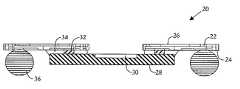
- FIG. 1shows a sectional side view of an integrated circuit package indicated generally by the numeral 20 .
- the integrated circuit package 20includes a substrate 22 having conductive traces therein. A cavity is disposed in the substrate 22 .
- a semiconductor die 28is mounted to a first surface 24 of the substrate 22 , in a flip-chip orientation such that a sensor portion 30 of the semiconductor die 28 is aligned with the cavity.
- Conductive interconnects 32connect pads of the semiconductor die 28 to the conductive traces of the substrate 22 .
- An underfill material 34surrounds the interconnects 32 .
- a plurality of conductive balls 36are disposed on the first surface 24 of the substrate 22 . The conductive balls 36 are electrically connected to the conductive traces such that ones of the conductive balls 36 are connected to ones of the pads of the semiconductor die 28 via the conductive traces.
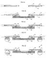
- the integrated circuit package 20will now be described in more detail with reference to FIGS. 2A to 2E to describe processing steps for fabricating the integrated circuit package 20 in accordance with an embodiment of the present invention.
- the substrate 22 of a bismaleimidetriazine (BT) resin/glass epoxy printed circuit boardis shown.
- the substrate 22includes conductive metal or alloy traces than provide conductive paths for signal transfer.
- the conductive tracesare patterned during manufacture of the substrate 22 .
- the substrate 22 manufacturing and patterning of the conductive tracesare well known and will be well understood by those skilled in the art.
- the substrate 22also includes the cavity that is formed using known techniques during manufacture of the substrate 22 and extends through the thickness of the substrate 22 , from the first surface 24 to an opposing second surface 26 .
- the substrate 22is in the form of a strip for producing a number of integrated circuit packages 20 . Only one such unit is depicted in FIGS. 2A to 2E , portions of adjacent units being shown by stippled lines.
- the present discussionrefers to the fabrication of a single integrated circuit package 20 for the purpose of simplicity only and it will be understood that the package 20 is preferably gang fabricated.
- the semiconductor die 28is then mounted in a flip-chip orientation by connection of the pads of the semiconductor die 28 to the conductive traces of the substrate 22 with the conductive interconnects 32 .
- solder ballswhich form the conductive interconnects 32 , are disposed on the semiconductor die 28 , using any of the established techniques available in the industry.
- the semiconductor die 28is then mounted on the substrate 22 via the conductive interconnects such that the sensor portion 30 of the semiconductor die 28 is aligned with the cavity of the substrate 22 , as shown. It will be appreciated that the pads of the semiconductor die 28 align with the portions of the conductive traces and the conductive interconnects 32 electrically connect the semiconductor die 28 with ones of the conductive traces of the substrate 22 .
- the underfill material 34surrounds the interconnects 32 and fills the area between the semiconductor die 28 and the substrate 22 , as shown in FIG. 2C . Care is taken to inhibit the underfill material 34 from covering the sensor portion 30 of the semiconductor die 30 , leaving the sensor portion 30 exposed to air.
- the plurality of conductive balls 36are placed on the first surface 24 of the substrate 22 , in connection with ones of the conductive traces of the substrate 22 , by conventional positioning ( FIG. 2D ).
- a fluxis added to the conductive balls 36 prior to placement and, after placement, the balls 36 are reflowed using known reflow techniques.
- the conductive balls 36are thereby connected to the conductive traces of the substrate 22 and through the interconnects 32 , to the semiconductor die 26 .
- the conductive balls 36provide signal and power connections as well as ground connections for the semiconductor die 28 .
- the conductive balls 36are suitably sized to provide clearance between a back side of the semiconductor die 28 and a printed circuit board surface (not shown) when the package 20 is mounted on a printed circuit board.
- Singulation of the individual integrated circuit package 20 from the stripis then performed either by saw singulation or die punching, resulting in the configuration shown in FIG. 2E .
- the individual package 20is isolated from other packages of the strip.
- FIGS. 3A to 3Gdescribe a process for manufacturing an integrated circuit package 20 according to another embodiment of the present invention.
- FIGS. 3A to 3Care similar to FIGS. 2A to 2C and therefore are not further described herein.
- a plurality of conductive balls 36are placed on the first surface 24 of the substrate 22 , in connection with ones of the conductive traces of the substrate 22 , by conventional positioning ( FIG. 3D ).
- a fluxis added to the conductive balls 36 prior to placement and, after placement, the balls 36 are reflowed using known reflow techniques.
- the conductive balls 36are thereby connected to the conductive traces of the substrate 22 and through the interconnects 32 , to the semiconductor die 26 .
- the conductive balls 36serve as I/O (input/output) redistribution balls, rather than serving as second level interconnects.
- the conductive balls 36are suitably sized to provide appropriate stand-off for the semiconductor die 28 .
- the back side of the semiconductor die 28 and the conductive balls 36are encapsulated in an overmold compound 38 such that the conductive balls 36 are exposed at a surface thereof, for providing a connection surface for attaching second level interconnect balls 40 .
- the second level interconnect balls 40are attached to the exposed surfaces of the conductive balls 36 by conventional positioning techniques ( FIG. 3F ).
- the second level interconnect balls 40are electrically connected to the semiconductor die 28 via the conductive balls 36 , the conductive traces of the substrate 22 and the interconnects 32 .
- Singulation of the individual integrated circuit package 20 from the stripis then performed either by saw singulation or die punching, resulting in the configuration shown in FIG. 3G .
- the individual package 20is isolated from other packages of the strip.
- FIG. 4An alternative embodiment of the package is shown in FIG. 4 in which the underfill material 34 covers the sensor portion 30 of the semiconductor die 30 rather than leaving the sensor portion 30 exposed to air.
- the sensor portion 30 of the semiconductor die 28is covered with the polymeric underfill material 34 or other material suitable for the package 20 being manufactured.
- a lid 42 of, for example, glassis attached to the second surface 26 of the substrate 22 , thereby covering and protecting the sensor portion 30 of the semiconductor die 28 , as shown in FIG. 5 .
- the lid 42is attached to the surface of the substrate 22 after underfilling with the underfill material 34 , as shown in FIG. 2C .
- a cleaning stepis added to remove possible contamination of the semiconductor die 28 , prior to attaching the lid 42 .
- the lidis then immediately attached to inhibit any contamination from the environment or assembly process from settling on the semiconductor die 28 .
- the lid 42protects the surface of the sensor portion 30 of the semiconductor die 28 .
- Other materialscan be used to cover the sensor portion 30 of the semiconductor die 28 , depending on the intended application of the integrated circuit package 20 . These materials are used, for example, for light filters, stress absorbers, ionic corrosion protection or many other functions. For example, for photonic applications, the sensor portion 30 is covered with either air accompanied by a glass lid or with a transparent encapsulant. In other exemplary applications, light filters are also employed. Clearly, transmission is an important aspect and appropriate materials are selected to inhibit selective blocking of desired wavelengths by package media. For a pressure sensor application, the sensor portion 30 is covered either with air or with a low stress encapsulant. In this application, appropriate materials are selected to inhibit thermally variable stresses exerted by packaging media on the die and to inhibit pressure damping by the material.
- a motion sensorincludes moveable parts and for this application the sensor portion 30 is covered by air.
- the substrate 22is not limited to the BT resin/glass epoxy printed circuit board as described and other suitable substrate materials can be employed.
- the conductive interconnects 32are not limited to solder ball conductive interconnects, as described. Other conductive interconnect materials can be used, including, for example, gold, copper, aluminum and conductive polymers.
Landscapes
- Engineering & Computer Science (AREA)
- Microelectronics & Electronic Packaging (AREA)
- Computer Hardware Design (AREA)
- Encapsulation Of And Coatings For Semiconductor Or Solid State Devices (AREA)
Abstract
Description
Claims (14)
Priority Applications (1)
| Application Number | Priority Date | Filing Date | Title |
|---|---|---|---|
| US10/759,247US6982491B1 (en) | 2004-01-20 | 2004-01-20 | Sensor semiconductor package and method of manufacturing the same |
Applications Claiming Priority (1)
| Application Number | Priority Date | Filing Date | Title |
|---|---|---|---|
| US10/759,247US6982491B1 (en) | 2004-01-20 | 2004-01-20 | Sensor semiconductor package and method of manufacturing the same |
Publications (1)
| Publication Number | Publication Date |
|---|---|
| US6982491B1true US6982491B1 (en) | 2006-01-03 |
Family
ID=35509047
Family Applications (1)
| Application Number | Title | Priority Date | Filing Date |
|---|---|---|---|
| US10/759,247Expired - LifetimeUS6982491B1 (en) | 2004-01-20 | 2004-01-20 | Sensor semiconductor package and method of manufacturing the same |
Country Status (1)
| Country | Link |
|---|---|
| US (1) | US6982491B1 (en) |
Cited By (40)
| Publication number | Priority date | Publication date | Assignee | Title |
|---|---|---|---|---|
| US20070063331A1 (en)* | 2005-09-16 | 2007-03-22 | Stats Chippac Ltd. | Integrated circuit package system with planar interconnects |
| US20080174977A1 (en)* | 2006-12-26 | 2008-07-24 | Akinobu Inoue | Electronic component contained substrate |
| US20090243082A1 (en)* | 2008-03-26 | 2009-10-01 | Zigmund Ramirez Camacho | Integrated circuit package system with planar interconnect |
| US20100052131A1 (en)* | 2008-08-26 | 2010-03-04 | Lionel Chien Hui Tay | Integrated circuit package system with redistribution layer |
| US20100123233A1 (en)* | 2008-11-18 | 2010-05-20 | In Sang Yoon | Integrated circuit package system and method of package stacking |
| US20100127363A1 (en)* | 2006-04-28 | 2010-05-27 | Utac Thai Limited | Very extremely thin semiconductor package |
| US7781852B1 (en)* | 2006-12-05 | 2010-08-24 | Amkor Technology, Inc. | Membrane die attach circuit element package and method therefor |
| US7790512B1 (en) | 2007-11-06 | 2010-09-07 | Utac Thai Limited | Molded leadframe substrate semiconductor package |
| US20100327432A1 (en)* | 2006-09-26 | 2010-12-30 | Utac Thai Limited | Package with heat transfer |
| US20110018111A1 (en)* | 2009-07-23 | 2011-01-27 | Utac Thai Limited | Leadframe feature to minimize flip-chip semiconductor die collapse during flip-chip reflow |
| US20110039371A1 (en)* | 2008-09-04 | 2011-02-17 | Utac Thai Limited | Flip chip cavity package |
| US20110133319A1 (en)* | 2009-12-04 | 2011-06-09 | Utac Thai Limited | Auxiliary leadframe member for stabilizing the bond wire process |
| US20110147931A1 (en)* | 2006-04-28 | 2011-06-23 | Utac Thai Limited | Lead frame land grid array with routing connector trace under unit |
| US20110198752A1 (en)* | 2006-04-28 | 2011-08-18 | Utac Thai Limited | Lead frame ball grid array with traces under die |
| US8013437B1 (en) | 2006-09-26 | 2011-09-06 | Utac Thai Limited | Package with heat transfer |
| US20110221051A1 (en)* | 2010-03-11 | 2011-09-15 | Utac Thai Limited | Leadframe based multi terminal ic package |
| US20110232693A1 (en)* | 2009-03-12 | 2011-09-29 | Utac Thai Limited | Metallic solderability preservation coating on metal part of semiconductor package to prevent oxide |
| US8063470B1 (en) | 2008-05-22 | 2011-11-22 | Utac Thai Limited | Method and apparatus for no lead semiconductor package |
| US20120034740A1 (en)* | 2008-04-24 | 2012-02-09 | Micron Technology, Inc. | Pre-encapsulated cavity interposer |
| US20120319262A1 (en)* | 2011-06-20 | 2012-12-20 | Heap Hoe Kuan | Integrated circuit packaging system with support structure and method of manufacture thereof |
| US20130043575A1 (en)* | 2011-08-17 | 2013-02-21 | Infineon Technologies Ag | Chip-packaging module for a chip and a method for forming a chip-packaging module |
| US8461694B1 (en) | 2006-04-28 | 2013-06-11 | Utac Thai Limited | Lead frame ball grid array with traces under die having interlocking features |
| US8460970B1 (en) | 2006-04-28 | 2013-06-11 | Utac Thai Limited | Lead frame ball grid array with traces under die having interlocking features |
| US8871571B2 (en) | 2010-04-02 | 2014-10-28 | Utac Thai Limited | Apparatus for and methods of attaching heat slugs to package tops |
| US9000590B2 (en) | 2012-05-10 | 2015-04-07 | Utac Thai Limited | Protruding terminals with internal routing interconnections semiconductor device |
| US9006034B1 (en) | 2012-06-11 | 2015-04-14 | Utac Thai Limited | Post-mold for semiconductor package having exposed traces |
| US9082607B1 (en) | 2006-12-14 | 2015-07-14 | Utac Thai Limited | Molded leadframe substrate semiconductor package |
| US9355940B1 (en) | 2009-12-04 | 2016-05-31 | Utac Thai Limited | Auxiliary leadframe member for stabilizing the bond wire process |
| US9449905B2 (en) | 2012-05-10 | 2016-09-20 | Utac Thai Limited | Plated terminals with routing interconnections semiconductor device |
| US9761435B1 (en) | 2006-12-14 | 2017-09-12 | Utac Thai Limited | Flip chip cavity package |
| US9805955B1 (en) | 2015-11-10 | 2017-10-31 | UTAC Headquarters Pte. Ltd. | Semiconductor package with multiple molding routing layers and a method of manufacturing the same |
| US20180174935A1 (en)* | 2016-12-13 | 2018-06-21 | Infineon Technologies Ag | Semiconductor package and method for fabricating a semiconductor package |
| US10242953B1 (en) | 2015-05-27 | 2019-03-26 | Utac Headquarters PTE. Ltd | Semiconductor package with plated metal shielding and a method thereof |
| US10242934B1 (en) | 2014-05-07 | 2019-03-26 | Utac Headquarters Pte Ltd. | Semiconductor package with full plating on contact side surfaces and methods thereof |
| US10276477B1 (en) | 2016-05-20 | 2019-04-30 | UTAC Headquarters Pte. Ltd. | Semiconductor package with multiple stacked leadframes and a method of manufacturing the same |
| CN110098157A (en)* | 2018-01-31 | 2019-08-06 | 三星电机株式会社 | Fan-out-type sensor package |
| US20200098965A1 (en)* | 2011-08-26 | 2020-03-26 | Micron Technology, Inc. | Solid-state radiation transducer devices having flip-chip mounted solid-state radiation transducers and associated systems and methods |
| US10989887B2 (en) | 2017-09-06 | 2021-04-27 | Agency For Science, Technology And Research | Photonic integrated circuit package and method of forming the same |
| US20220270960A1 (en)* | 2021-02-23 | 2022-08-25 | Texas Instruments Incorporated | Open-Cavity Package for Chip Sensor |
| US20230067914A1 (en)* | 2021-08-31 | 2023-03-02 | Taiwan Semiconductor Manufacturing Company, Ltd. | Semiconductor package and manufacturing method thereof |
Citations (19)
| Publication number | Priority date | Publication date | Assignee | Title |
|---|---|---|---|---|
| US5900675A (en)* | 1997-04-21 | 1999-05-04 | International Business Machines Corporation | Organic controlled collapse chip connector (C4) ball grid array (BGA) chip carrier with dual thermal expansion rates |
| US6084308A (en)* | 1998-06-30 | 2000-07-04 | National Semiconductor Corporation | Chip-on-chip integrated circuit package and method for making the same |
| US6114755A (en)* | 1996-05-24 | 2000-09-05 | Sony Corporation | Semiconductor package including chip housing, encapsulation and the manufacturing method |
| US20010001505A1 (en)* | 1998-10-14 | 2001-05-24 | 3M Innovative Properties Company | Tape ball grid array with interconnected ground plane |
| US6380631B2 (en)* | 1999-08-30 | 2002-04-30 | Micron Technology Inc. | Apparatus and methods of packaging and testing die |
| US20020081755A1 (en)* | 2000-12-22 | 2002-06-27 | Yinon Degani | Method of testing and constructing monolithic multi-chip modules |
| US20020127771A1 (en)* | 2001-03-12 | 2002-09-12 | Salman Akram | Multiple die package |
| US20020130422A1 (en)* | 2001-03-15 | 2002-09-19 | Vaiyapuri Venkateshwaran | Semiconductor/printed circuit board assembly, and computer system |
| US6469897B2 (en)* | 2001-01-30 | 2002-10-22 | Siliconware Precision Industries Co., Ltd. | Cavity-down tape ball grid array package assembly with grounded heat sink and method of fabricating the same |
| US6483187B1 (en)* | 2000-07-04 | 2002-11-19 | Advanced Semiconductor Engineering, Inc. | Heat-spread substrate |
| US6528869B1 (en)* | 2001-04-06 | 2003-03-04 | Amkor Technology, Inc. | Semiconductor package with molded substrate and recessed input/output terminals |
| US6599774B2 (en)* | 1999-06-29 | 2003-07-29 | International Business Machines Corporation | Technique for underfilling stacked chips on a cavity MLC module |
| US20030151148A1 (en)* | 2000-11-06 | 2003-08-14 | St Assembly Test Services Pte Ltd | Single unit automated assembly of flex enhanced ball grid array packages |
| US6656768B2 (en)* | 2001-02-08 | 2003-12-02 | Texas Instruments Incorporated | Flip-chip assembly of protected micromechanical devices |
| US20040080046A1 (en)* | 2002-10-29 | 2004-04-29 | Lee Choon Kuan | Semiconductor package having multi-layer leadframe and method of fabrication |
| US6744125B2 (en)* | 2001-05-30 | 2004-06-01 | St. Assembly Test Services Ltd. | Super thin/super thermal ball grid array package |
| US20050046039A1 (en)* | 2003-08-27 | 2005-03-03 | Advanced Semiconductor Engineering, Inc. | Flip-chip package |
| US20050051859A1 (en)* | 2001-10-25 | 2005-03-10 | Amkor Technology, Inc. | Look down image sensor package |
| US6879031B2 (en)* | 2003-04-23 | 2005-04-12 | Advanced Semiconductor Engineering, Inc. | Multi-chips package |
- 2004
- 2004-01-20USUS10/759,247patent/US6982491B1/ennot_activeExpired - Lifetime
Patent Citations (20)
| Publication number | Priority date | Publication date | Assignee | Title |
|---|---|---|---|---|
| US6114755A (en)* | 1996-05-24 | 2000-09-05 | Sony Corporation | Semiconductor package including chip housing, encapsulation and the manufacturing method |
| US5900675A (en)* | 1997-04-21 | 1999-05-04 | International Business Machines Corporation | Organic controlled collapse chip connector (C4) ball grid array (BGA) chip carrier with dual thermal expansion rates |
| US6084308A (en)* | 1998-06-30 | 2000-07-04 | National Semiconductor Corporation | Chip-on-chip integrated circuit package and method for making the same |
| US20010001505A1 (en)* | 1998-10-14 | 2001-05-24 | 3M Innovative Properties Company | Tape ball grid array with interconnected ground plane |
| US6599774B2 (en)* | 1999-06-29 | 2003-07-29 | International Business Machines Corporation | Technique for underfilling stacked chips on a cavity MLC module |
| US6380631B2 (en)* | 1999-08-30 | 2002-04-30 | Micron Technology Inc. | Apparatus and methods of packaging and testing die |
| US20040084738A1 (en)* | 2000-02-22 | 2004-05-06 | Sunil Thomas | Flip-chip assembly of protected micromechanical devices |
| US6483187B1 (en)* | 2000-07-04 | 2002-11-19 | Advanced Semiconductor Engineering, Inc. | Heat-spread substrate |
| US20030151148A1 (en)* | 2000-11-06 | 2003-08-14 | St Assembly Test Services Pte Ltd | Single unit automated assembly of flex enhanced ball grid array packages |
| US20020081755A1 (en)* | 2000-12-22 | 2002-06-27 | Yinon Degani | Method of testing and constructing monolithic multi-chip modules |
| US6469897B2 (en)* | 2001-01-30 | 2002-10-22 | Siliconware Precision Industries Co., Ltd. | Cavity-down tape ball grid array package assembly with grounded heat sink and method of fabricating the same |
| US6656768B2 (en)* | 2001-02-08 | 2003-12-02 | Texas Instruments Incorporated | Flip-chip assembly of protected micromechanical devices |
| US20020127771A1 (en)* | 2001-03-12 | 2002-09-12 | Salman Akram | Multiple die package |
| US20020130422A1 (en)* | 2001-03-15 | 2002-09-19 | Vaiyapuri Venkateshwaran | Semiconductor/printed circuit board assembly, and computer system |
| US6528869B1 (en)* | 2001-04-06 | 2003-03-04 | Amkor Technology, Inc. | Semiconductor package with molded substrate and recessed input/output terminals |
| US6744125B2 (en)* | 2001-05-30 | 2004-06-01 | St. Assembly Test Services Ltd. | Super thin/super thermal ball grid array package |
| US20050051859A1 (en)* | 2001-10-25 | 2005-03-10 | Amkor Technology, Inc. | Look down image sensor package |
| US20040080046A1 (en)* | 2002-10-29 | 2004-04-29 | Lee Choon Kuan | Semiconductor package having multi-layer leadframe and method of fabrication |
| US6879031B2 (en)* | 2003-04-23 | 2005-04-12 | Advanced Semiconductor Engineering, Inc. | Multi-chips package |
| US20050046039A1 (en)* | 2003-08-27 | 2005-03-03 | Advanced Semiconductor Engineering, Inc. | Flip-chip package |
Non-Patent Citations (1)
| Title |
|---|
| Dr. Ken Gilleo, MEMS Packaging Issues and Materials, Cookson Electronics. |
Cited By (91)
| Publication number | Priority date | Publication date | Assignee | Title |
|---|---|---|---|---|
| US20070063331A1 (en)* | 2005-09-16 | 2007-03-22 | Stats Chippac Ltd. | Integrated circuit package system with planar interconnects |
| US8067831B2 (en)* | 2005-09-16 | 2011-11-29 | Stats Chippac Ltd. | Integrated circuit package system with planar interconnects |
| US8652879B2 (en) | 2006-04-28 | 2014-02-18 | Utac Thai Limited | Lead frame ball grid array with traces under die |
| US8704381B2 (en) | 2006-04-28 | 2014-04-22 | Utac Thai Limited | Very extremely thin semiconductor package |
| US8685794B2 (en) | 2006-04-28 | 2014-04-01 | Utac Thai Limited | Lead frame land grid array with routing connector trace under unit |
| US20100127363A1 (en)* | 2006-04-28 | 2010-05-27 | Utac Thai Limited | Very extremely thin semiconductor package |
| US9099317B2 (en) | 2006-04-28 | 2015-08-04 | Utac Thai Limited | Method for forming lead frame land grid array |
| US8575762B2 (en) | 2006-04-28 | 2013-11-05 | Utac Thai Limited | Very extremely thin semiconductor package |
| US8492906B2 (en) | 2006-04-28 | 2013-07-23 | Utac Thai Limited | Lead frame ball grid array with traces under die |
| US8487451B2 (en) | 2006-04-28 | 2013-07-16 | Utac Thai Limited | Lead frame land grid array with routing connector trace under unit |
| US8460970B1 (en) | 2006-04-28 | 2013-06-11 | Utac Thai Limited | Lead frame ball grid array with traces under die having interlocking features |
| US8461694B1 (en) | 2006-04-28 | 2013-06-11 | Utac Thai Limited | Lead frame ball grid array with traces under die having interlocking features |
| US8310060B1 (en) | 2006-04-28 | 2012-11-13 | Utac Thai Limited | Lead frame land grid array |
| US20110147931A1 (en)* | 2006-04-28 | 2011-06-23 | Utac Thai Limited | Lead frame land grid array with routing connector trace under unit |
| US20110198752A1 (en)* | 2006-04-28 | 2011-08-18 | Utac Thai Limited | Lead frame ball grid array with traces under die |
| US8125077B2 (en) | 2006-09-26 | 2012-02-28 | Utac Thai Limited | Package with heat transfer |
| US8013437B1 (en) | 2006-09-26 | 2011-09-06 | Utac Thai Limited | Package with heat transfer |
| US20100327432A1 (en)* | 2006-09-26 | 2010-12-30 | Utac Thai Limited | Package with heat transfer |
| US7781852B1 (en)* | 2006-12-05 | 2010-08-24 | Amkor Technology, Inc. | Membrane die attach circuit element package and method therefor |
| US9196470B1 (en) | 2006-12-14 | 2015-11-24 | Utac Thai Limited | Molded leadframe substrate semiconductor package |
| US9899208B2 (en) | 2006-12-14 | 2018-02-20 | Utac Thai Limited | Molded leadframe substrate semiconductor package |
| US9082607B1 (en) | 2006-12-14 | 2015-07-14 | Utac Thai Limited | Molded leadframe substrate semiconductor package |
| US9711343B1 (en) | 2006-12-14 | 2017-07-18 | Utac Thai Limited | Molded leadframe substrate semiconductor package |
| US9093486B2 (en) | 2006-12-14 | 2015-07-28 | Utac Thai Limited | Molded leadframe substrate semiconductor package |
| US9761435B1 (en) | 2006-12-14 | 2017-09-12 | Utac Thai Limited | Flip chip cavity package |
| US9099294B1 (en) | 2006-12-14 | 2015-08-04 | Utac Thai Limited | Molded leadframe substrate semiconductor package |
| US7872359B2 (en)* | 2006-12-26 | 2011-01-18 | Shinko Electric Industries Co., Ltd. | Electronic component contained substrate |
| US20080174977A1 (en)* | 2006-12-26 | 2008-07-24 | Akinobu Inoue | Electronic component contained substrate |
| US8338922B1 (en) | 2007-11-06 | 2012-12-25 | Utac Thai Limited | Molded leadframe substrate semiconductor package |
| US7790512B1 (en) | 2007-11-06 | 2010-09-07 | Utac Thai Limited | Molded leadframe substrate semiconductor package |
| US9059074B2 (en) | 2008-03-26 | 2015-06-16 | Stats Chippac Ltd. | Integrated circuit package system with planar interconnect |
| US20090243082A1 (en)* | 2008-03-26 | 2009-10-01 | Zigmund Ramirez Camacho | Integrated circuit package system with planar interconnect |
| US20120034740A1 (en)* | 2008-04-24 | 2012-02-09 | Micron Technology, Inc. | Pre-encapsulated cavity interposer |
| US8399297B2 (en)* | 2008-04-24 | 2013-03-19 | Micron Technology, Inc. | Methods of forming and assembling pre-encapsulated assemblies and of forming associated semiconductor device packages |
| US8071426B2 (en) | 2008-05-22 | 2011-12-06 | Utac Thai Limited | Method and apparatus for no lead semiconductor package |
| US8063470B1 (en) | 2008-05-22 | 2011-11-22 | Utac Thai Limited | Method and apparatus for no lead semiconductor package |
| US20100052131A1 (en)* | 2008-08-26 | 2010-03-04 | Lionel Chien Hui Tay | Integrated circuit package system with redistribution layer |
| US8043894B2 (en) | 2008-08-26 | 2011-10-25 | Stats Chippac Ltd. | Integrated circuit package system with redistribution layer |
| US20110039371A1 (en)* | 2008-09-04 | 2011-02-17 | Utac Thai Limited | Flip chip cavity package |
| US9947605B2 (en) | 2008-09-04 | 2018-04-17 | UTAC Headquarters Pte. Ltd. | Flip chip cavity package |
| US20100123233A1 (en)* | 2008-11-18 | 2010-05-20 | In Sang Yoon | Integrated circuit package system and method of package stacking |
| US8130512B2 (en)* | 2008-11-18 | 2012-03-06 | Stats Chippac Ltd. | Integrated circuit package system and method of package stacking |
| US8431443B2 (en) | 2009-03-12 | 2013-04-30 | Utac Thai Limited | Metallic solderability preservation coating on metal part of semiconductor package to prevent oxide |
| US8569877B2 (en) | 2009-03-12 | 2013-10-29 | Utac Thai Limited | Metallic solderability preservation coating on metal part of semiconductor package to prevent oxide |
| US8367476B2 (en) | 2009-03-12 | 2013-02-05 | Utac Thai Limited | Metallic solderability preservation coating on metal part of semiconductor package to prevent oxide |
| US20110232693A1 (en)* | 2009-03-12 | 2011-09-29 | Utac Thai Limited | Metallic solderability preservation coating on metal part of semiconductor package to prevent oxide |
| US9449900B2 (en) | 2009-07-23 | 2016-09-20 | UTAC Headquarters Pte. Ltd. | Leadframe feature to minimize flip-chip semiconductor die collapse during flip-chip reflow |
| US20110018111A1 (en)* | 2009-07-23 | 2011-01-27 | Utac Thai Limited | Leadframe feature to minimize flip-chip semiconductor die collapse during flip-chip reflow |
| US9355940B1 (en) | 2009-12-04 | 2016-05-31 | Utac Thai Limited | Auxiliary leadframe member for stabilizing the bond wire process |
| US8368189B2 (en) | 2009-12-04 | 2013-02-05 | Utac Thai Limited | Auxiliary leadframe member for stabilizing the bond wire process |
| US20110133319A1 (en)* | 2009-12-04 | 2011-06-09 | Utac Thai Limited | Auxiliary leadframe member for stabilizing the bond wire process |
| US8722461B2 (en) | 2010-03-11 | 2014-05-13 | Utac Thai Limited | Leadframe based multi terminal IC package |
| US20110221051A1 (en)* | 2010-03-11 | 2011-09-15 | Utac Thai Limited | Leadframe based multi terminal ic package |
| US8575732B2 (en) | 2010-03-11 | 2013-11-05 | Utac Thai Limited | Leadframe based multi terminal IC package |
| US8871571B2 (en) | 2010-04-02 | 2014-10-28 | Utac Thai Limited | Apparatus for and methods of attaching heat slugs to package tops |
| US20120319262A1 (en)* | 2011-06-20 | 2012-12-20 | Heap Hoe Kuan | Integrated circuit packaging system with support structure and method of manufacture thereof |
| US8642382B2 (en)* | 2011-06-20 | 2014-02-04 | Stats Chippac Ltd. | Integrated circuit packaging system with support structure and method of manufacture thereof |
| US20130043575A1 (en)* | 2011-08-17 | 2013-02-21 | Infineon Technologies Ag | Chip-packaging module for a chip and a method for forming a chip-packaging module |
| US9324586B2 (en)* | 2011-08-17 | 2016-04-26 | Infineon Technologies Ag | Chip-packaging module for a chip and a method for forming a chip-packaging module |
| US20200098965A1 (en)* | 2011-08-26 | 2020-03-26 | Micron Technology, Inc. | Solid-state radiation transducer devices having flip-chip mounted solid-state radiation transducers and associated systems and methods |
| US11929456B2 (en)* | 2011-08-26 | 2024-03-12 | Lodestar Licensing Group Llc | Solid-state radiation transducer devices having flip-chip mounted solid-state radiation transducers and associated systems and methods |
| US9922914B2 (en) | 2012-05-10 | 2018-03-20 | Utac Thai Limited | Plated terminals with routing interconnections semiconductor device |
| US9449905B2 (en) | 2012-05-10 | 2016-09-20 | Utac Thai Limited | Plated terminals with routing interconnections semiconductor device |
| US9922913B2 (en) | 2012-05-10 | 2018-03-20 | Utac Thai Limited | Plated terminals with routing interconnections semiconductor device |
| US9000590B2 (en) | 2012-05-10 | 2015-04-07 | Utac Thai Limited | Protruding terminals with internal routing interconnections semiconductor device |
| US9972563B2 (en) | 2012-05-10 | 2018-05-15 | UTAC Headquarters Pte. Ltd. | Plated terminals with routing interconnections semiconductor device |
| US9029198B2 (en) | 2012-05-10 | 2015-05-12 | Utac Thai Limited | Methods of manufacturing semiconductor devices including terminals with internal routing interconnections |
| US9397031B2 (en) | 2012-06-11 | 2016-07-19 | Utac Thai Limited | Post-mold for semiconductor package having exposed traces |
| US9006034B1 (en) | 2012-06-11 | 2015-04-14 | Utac Thai Limited | Post-mold for semiconductor package having exposed traces |
| US10242934B1 (en) | 2014-05-07 | 2019-03-26 | Utac Headquarters Pte Ltd. | Semiconductor package with full plating on contact side surfaces and methods thereof |
| US10269686B1 (en) | 2015-05-27 | 2019-04-23 | UTAC Headquarters PTE, LTD. | Method of improving adhesion between molding compounds and an apparatus thereof |
| US10242953B1 (en) | 2015-05-27 | 2019-03-26 | Utac Headquarters PTE. Ltd | Semiconductor package with plated metal shielding and a method thereof |
| US9922843B1 (en) | 2015-11-10 | 2018-03-20 | UTAC Headquarters Pte. Ltd. | Semiconductor package with multiple molding routing layers and a method of manufacturing the same |
| US10163658B2 (en) | 2015-11-10 | 2018-12-25 | UTAC Headquarters PTE, LTD. | Semiconductor package with multiple molding routing layers and a method of manufacturing the same |
| US10096490B2 (en) | 2015-11-10 | 2018-10-09 | UTAC Headquarters Pte. Ltd. | Semiconductor package with multiple molding routing layers and a method of manufacturing the same |
| US10032645B1 (en) | 2015-11-10 | 2018-07-24 | UTAC Headquarters Pte. Ltd. | Semiconductor package with multiple molding routing layers and a method of manufacturing the same |
| US9917038B1 (en) | 2015-11-10 | 2018-03-13 | Utac Headquarters Pte Ltd | Semiconductor package with multiple molding routing layers and a method of manufacturing the same |
| US10325782B2 (en) | 2015-11-10 | 2019-06-18 | UTAC Headquarters Pte. Ltd. | Semiconductor package with multiple molding routing layers and a method of manufacturing the same |
| US9805955B1 (en) | 2015-11-10 | 2017-10-31 | UTAC Headquarters Pte. Ltd. | Semiconductor package with multiple molding routing layers and a method of manufacturing the same |
| US10734247B2 (en) | 2015-11-10 | 2020-08-04 | Utac Headquarters PTE. Ltd | Semiconductor package with multiple molding routing layers and a method of manufacturing the same |
| US10276477B1 (en) | 2016-05-20 | 2019-04-30 | UTAC Headquarters Pte. Ltd. | Semiconductor package with multiple stacked leadframes and a method of manufacturing the same |
| US20180174935A1 (en)* | 2016-12-13 | 2018-06-21 | Infineon Technologies Ag | Semiconductor package and method for fabricating a semiconductor package |
| US10490470B2 (en)* | 2016-12-13 | 2019-11-26 | Infineon Technologies Ag | Semiconductor package and method for fabricating a semiconductor package |
| US10989887B2 (en) | 2017-09-06 | 2021-04-27 | Agency For Science, Technology And Research | Photonic integrated circuit package and method of forming the same |
| TWI684251B (en)* | 2018-01-31 | 2020-02-01 | 南韓商三星電機股份有限公司 | Fan-out sensor package |
| US10748828B2 (en)* | 2018-01-31 | 2020-08-18 | Samsung Electro-Mechanics Co., Ltd. | Fan-out sensor package |
| CN110098157B (en)* | 2018-01-31 | 2023-04-14 | 三星电机株式会社 | Fan-out sensor package |
| CN110098157A (en)* | 2018-01-31 | 2019-08-06 | 三星电机株式会社 | Fan-out-type sensor package |
| US20220270960A1 (en)* | 2021-02-23 | 2022-08-25 | Texas Instruments Incorporated | Open-Cavity Package for Chip Sensor |
| US20230067914A1 (en)* | 2021-08-31 | 2023-03-02 | Taiwan Semiconductor Manufacturing Company, Ltd. | Semiconductor package and manufacturing method thereof |
| US11908764B2 (en)* | 2021-08-31 | 2024-02-20 | Taiwan Semiconductor Manufacturing Company, Ltd. | Semiconductor package including a circuit substrate having a cavity and a floor plate embedded in a dielectric material and a semiconductor die disposed in the cavity |
Similar Documents
| Publication | Publication Date | Title |
|---|---|---|
| US6982491B1 (en) | Sensor semiconductor package and method of manufacturing the same | |
| US7091062B2 (en) | Wafer level packages for chips with sawn edge protection | |
| US10090185B2 (en) | Semiconductor device and manufacturing method thereof | |
| KR101837808B1 (en) | Wire bond sensor package and method | |
| US7205674B2 (en) | Semiconductor package with build-up layers formed on chip and fabrication method of the semiconductor package | |
| KR101336569B1 (en) | Semiconductor Packages With Enhanced Joint Reliability And Methods Of Fabricating The Same | |
| KR101683688B1 (en) | Integrated circuit package and method for manufacturing an integrated circuit package | |
| KR101722264B1 (en) | Integrated circuit devices and semiconductor device package with through-body conductive vias, and methods of making semiconductor device | |
| CN101217156B (en) | Chip scale packaging and manufacturing method of electronic component and CMOS image sensor | |
| US7019406B2 (en) | Thermally enhanced semiconductor package | |
| KR100393448B1 (en) | Semiconductor package and method for manufacturing the same | |
| US20040140557A1 (en) | Wl-bga for MEMS/MOEMS devices | |
| US20090186446A1 (en) | Semiconductor device packages and methods of fabricating the same | |
| US10566369B2 (en) | Image sensor with processor package | |
| US20110180891A1 (en) | Conductor package structure and method of the same | |
| WO2008091717A1 (en) | Wafer level csp packaging concept | |
| US10115673B1 (en) | Embedded substrate package structure | |
| US9412729B2 (en) | Semiconductor package and fabricating method thereof | |
| US20210050275A1 (en) | Fan-out semiconductor package structure and packaging method thereof | |
| US7868472B2 (en) | Thermal dissipation in integrated circuit systems | |
| KR20140126137A (en) | Method of manufacturing Semiconductor package | |
| US10622270B2 (en) | Integrated circuit package with stress directing material | |
| CN217062077U (en) | Packaging structure | |
| TWI884189B (en) | Electronic devices and methods of manufacturing electronic devices | |
| US20250311456A1 (en) | Semiconductor package |
Legal Events
| Date | Code | Title | Description |
|---|---|---|---|
| AS | Assignment | Owner name:ASAT LTD., HONG KONG Free format text:ASSIGNMENT OF ASSIGNORS INTEREST;ASSIGNORS:FAN, CHUN HO;LABEEB, SADAK THAMBY;CHOW, LAP KEUNG;REEL/FRAME:014735/0253;SIGNING DATES FROM 20040206 TO 20040214 | |
| STCF | Information on status: patent grant | Free format text:PATENTED CASE | |
| FPAY | Fee payment | Year of fee payment:4 | |
| FEPP | Fee payment procedure | Free format text:PAYOR NUMBER ASSIGNED (ORIGINAL EVENT CODE: ASPN); ENTITY STATUS OF PATENT OWNER: LARGE ENTITY Free format text:PAYER NUMBER DE-ASSIGNED (ORIGINAL EVENT CODE: RMPN); ENTITY STATUS OF PATENT OWNER: LARGE ENTITY | |
| AS | Assignment | Owner name:JPMORGAN CHASE BANK, N.A., AS COLLATERAL AGENT,TEX Free format text:GRANT OF SECURITY INTEREST IN PATENT RIGHTS - FIRST PRIORITY;ASSIGNOR:UTAC HONG KONG LIMITED;REEL/FRAME:024599/0743 Effective date:20100604 Owner name:JPMORGAN CHASE BANK, N.A., AS COLLATERAL AGENT,TEX Free format text:GRANT OF SECURITY INTEREST IN PATENT RIGHTS - SECOND PRIORITY;ASSIGNOR:UTAC HONG KONG LIMITED;REEL/FRAME:024599/0827 Effective date:20100604 Owner name:THE HONGKONG AND SHANGHAI BANKING CORPORATION LIMI Free format text:GRANT OF SECURITY INTEREST IN PATENT RIGHTS - SECOND PRIORITY;ASSIGNOR:UTAC HONG KONG LIMITED;REEL/FRAME:024611/0097 Effective date:20100604 Owner name:JPMORGAN CHASE BANK, N.A., AS COLLATERAL AGENT, TE Free format text:GRANT OF SECURITY INTEREST IN PATENT RIGHTS - FIRST PRIORITY;ASSIGNOR:UTAC HONG KONG LIMITED;REEL/FRAME:024599/0743 Effective date:20100604 Owner name:JPMORGAN CHASE BANK, N.A., AS COLLATERAL AGENT, TE Free format text:GRANT OF SECURITY INTEREST IN PATENT RIGHTS - SECOND PRIORITY;ASSIGNOR:UTAC HONG KONG LIMITED;REEL/FRAME:024599/0827 Effective date:20100604 | |
| AS | Assignment | Owner name:UTAC HONG KONG LIMITED, HONG KONG Free format text:CHANGE OF NAME;ASSIGNOR:ASAT LIMITED;REEL/FRAME:025217/0340 Effective date:20100325 | |
| FPAY | Fee payment | Year of fee payment:8 | |
| AS | Assignment | Owner name:UTAC HEADQUARTERS PTE. LTD., SINGAPORE Free format text:ASSIGNMENT OF ASSIGNORS INTEREST;ASSIGNOR:UTAC HONG KONG LIMITED;REEL/FRAME:037880/0534 Effective date:20150508 | |
| AS | Assignment | Owner name:UTAC HEADQUARTERS PTE. LTD., SINGAPORE Free format text:CORRECTIVE ASSIGNMENT TO CORRECT THE ADD ANNEX INADVERTENTLY LEFT OUT ORIGINAL ASSIGNMENT DOCUMENT PREVIOUSLY RECORDED AT REEL: 037880 FRAME: 0534. ASSIGNOR(S) HEREBY CONFIRMS THE ASSIGNMENT;ASSIGNOR:UTAC HONG KONG LIMITED;REEL/FRAME:039822/0591 Effective date:20150508 | |
| FPAY | Fee payment | Year of fee payment:12 |