US6981832B2 - Wafer handling system - Google Patents
Wafer handling systemDownload PDFInfo
- Publication number
- US6981832B2 US6981832B2US10/641,807US64180703AUS6981832B2US 6981832 B2US6981832 B2US 6981832B2US 64180703 AUS64180703 AUS 64180703AUS 6981832 B2US6981832 B2US 6981832B2
- Authority
- US
- United States
- Prior art keywords
- cassette
- foup
- cassettes
- wafer
- handler
- Prior art date
- Legal status (The legal status is an assumption and is not a legal conclusion. Google has not performed a legal analysis and makes no representation as to the accuracy of the status listed.)
- Expired - Fee Related, expires
Links
- 235000012431wafersNutrition0.000claimsabstractdescription153
- 238000012546transferMethods0.000claimsabstractdescription97
- 238000012545processingMethods0.000claimsabstractdescription69
- 239000012636effectorSubstances0.000claimsabstractdescription22
- 238000005192partitionMethods0.000claimsdescription19
- 230000007246mechanismEffects0.000claimsdescription13
- 230000004308accommodationEffects0.000claims3
- 230000013011matingEffects0.000claims1
- 230000006978adaptationEffects0.000abstractdescription4
- 239000004065semiconductorSubstances0.000abstractdescription4
- 238000001514detection methodMethods0.000description6
- 238000000034methodMethods0.000description5
- 238000004519manufacturing processMethods0.000description4
- 238000003780insertionMethods0.000description3
- 230000037431insertionEffects0.000description3
- 230000003993interactionEffects0.000description3
- 230000008901benefitEffects0.000description2
- 238000004891communicationMethods0.000description2
- 230000005484gravityEffects0.000description2
- 230000003287optical effectEffects0.000description2
- 230000008569processEffects0.000description2
- 239000004696Poly ether ether ketoneSubstances0.000description1
- 238000007792additionMethods0.000description1
- 238000004458analytical methodMethods0.000description1
- 238000013459approachMethods0.000description1
- JUPQTSLXMOCDHR-UHFFFAOYSA-Nbenzene-1,4-diol;bis(4-fluorophenyl)methanoneChemical compoundOC1=CC=C(O)C=C1.C1=CC(F)=CC=C1C(=O)C1=CC=C(F)C=C1JUPQTSLXMOCDHR-UHFFFAOYSA-N0.000description1
- 230000003247decreasing effectEffects0.000description1
- 238000013461designMethods0.000description1
- 238000009429electrical wiringMethods0.000description1
- 238000005516engineering processMethods0.000description1
- 238000009434installationMethods0.000description1
- 239000000463materialSubstances0.000description1
- 238000012986modificationMethods0.000description1
- 230000004048modificationEffects0.000description1
- 229920002530polyetherether ketonePolymers0.000description1
- 239000000758substrateSubstances0.000description1
- 230000032258transportEffects0.000description1
Images


Classifications
- H—ELECTRICITY
- H01—ELECTRIC ELEMENTS
- H01L—SEMICONDUCTOR DEVICES NOT COVERED BY CLASS H10
- H01L21/00—Processes or apparatus adapted for the manufacture or treatment of semiconductor or solid state devices or of parts thereof
- H01L21/67—Apparatus specially adapted for handling semiconductor or electric solid state devices during manufacture or treatment thereof; Apparatus specially adapted for handling wafers during manufacture or treatment of semiconductor or electric solid state devices or components ; Apparatus not specifically provided for elsewhere
- H01L21/68—Apparatus specially adapted for handling semiconductor or electric solid state devices during manufacture or treatment thereof; Apparatus specially adapted for handling wafers during manufacture or treatment of semiconductor or electric solid state devices or components ; Apparatus not specifically provided for elsewhere for positioning, orientation or alignment
- H—ELECTRICITY
- H01—ELECTRIC ELEMENTS
- H01L—SEMICONDUCTOR DEVICES NOT COVERED BY CLASS H10
- H01L21/00—Processes or apparatus adapted for the manufacture or treatment of semiconductor or solid state devices or of parts thereof
- H01L21/67—Apparatus specially adapted for handling semiconductor or electric solid state devices during manufacture or treatment thereof; Apparatus specially adapted for handling wafers during manufacture or treatment of semiconductor or electric solid state devices or components ; Apparatus not specifically provided for elsewhere
- H01L21/677—Apparatus specially adapted for handling semiconductor or electric solid state devices during manufacture or treatment thereof; Apparatus specially adapted for handling wafers during manufacture or treatment of semiconductor or electric solid state devices or components ; Apparatus not specifically provided for elsewhere for conveying, e.g. between different workstations
- H01L21/67739—Apparatus specially adapted for handling semiconductor or electric solid state devices during manufacture or treatment thereof; Apparatus specially adapted for handling wafers during manufacture or treatment of semiconductor or electric solid state devices or components ; Apparatus not specifically provided for elsewhere for conveying, e.g. between different workstations into and out of processing chamber
- H01L21/67757—Apparatus specially adapted for handling semiconductor or electric solid state devices during manufacture or treatment thereof; Apparatus specially adapted for handling wafers during manufacture or treatment of semiconductor or electric solid state devices or components ; Apparatus not specifically provided for elsewhere for conveying, e.g. between different workstations into and out of processing chamber vertical transfer of a batch of workpieces
- H—ELECTRICITY
- H01—ELECTRIC ELEMENTS
- H01L—SEMICONDUCTOR DEVICES NOT COVERED BY CLASS H10
- H01L21/00—Processes or apparatus adapted for the manufacture or treatment of semiconductor or solid state devices or of parts thereof
- H01L21/67—Apparatus specially adapted for handling semiconductor or electric solid state devices during manufacture or treatment thereof; Apparatus specially adapted for handling wafers during manufacture or treatment of semiconductor or electric solid state devices or components ; Apparatus not specifically provided for elsewhere
- H01L21/673—Apparatus specially adapted for handling semiconductor or electric solid state devices during manufacture or treatment thereof; Apparatus specially adapted for handling wafers during manufacture or treatment of semiconductor or electric solid state devices or components ; Apparatus not specifically provided for elsewhere using specially adapted carriers or holders; Fixing the workpieces on such carriers or holders
- H01L21/6735—Closed carriers
- H01L21/67379—Closed carriers characterised by coupling elements, kinematic members, handles or elements to be externally gripped
- H—ELECTRICITY
- H01—ELECTRIC ELEMENTS
- H01L—SEMICONDUCTOR DEVICES NOT COVERED BY CLASS H10
- H01L21/00—Processes or apparatus adapted for the manufacture or treatment of semiconductor or solid state devices or of parts thereof
- H01L21/67—Apparatus specially adapted for handling semiconductor or electric solid state devices during manufacture or treatment thereof; Apparatus specially adapted for handling wafers during manufacture or treatment of semiconductor or electric solid state devices or components ; Apparatus not specifically provided for elsewhere
- H01L21/673—Apparatus specially adapted for handling semiconductor or electric solid state devices during manufacture or treatment thereof; Apparatus specially adapted for handling wafers during manufacture or treatment of semiconductor or electric solid state devices or components ; Apparatus not specifically provided for elsewhere using specially adapted carriers or holders; Fixing the workpieces on such carriers or holders
- H01L21/6735—Closed carriers
- H01L21/67386—Closed carriers characterised by the construction of the closed carrier
- H—ELECTRICITY
- H01—ELECTRIC ELEMENTS
- H01L—SEMICONDUCTOR DEVICES NOT COVERED BY CLASS H10
- H01L21/00—Processes or apparatus adapted for the manufacture or treatment of semiconductor or solid state devices or of parts thereof
- H01L21/67—Apparatus specially adapted for handling semiconductor or electric solid state devices during manufacture or treatment thereof; Apparatus specially adapted for handling wafers during manufacture or treatment of semiconductor or electric solid state devices or components ; Apparatus not specifically provided for elsewhere
- H01L21/677—Apparatus specially adapted for handling semiconductor or electric solid state devices during manufacture or treatment thereof; Apparatus specially adapted for handling wafers during manufacture or treatment of semiconductor or electric solid state devices or components ; Apparatus not specifically provided for elsewhere for conveying, e.g. between different workstations
- H01L21/67763—Apparatus specially adapted for handling semiconductor or electric solid state devices during manufacture or treatment thereof; Apparatus specially adapted for handling wafers during manufacture or treatment of semiconductor or electric solid state devices or components ; Apparatus not specifically provided for elsewhere for conveying, e.g. between different workstations the wafers being stored in a carrier, involving loading and unloading
- H01L21/67769—Storage means
- H—ELECTRICITY
- H01—ELECTRIC ELEMENTS
- H01L—SEMICONDUCTOR DEVICES NOT COVERED BY CLASS H10
- H01L21/00—Processes or apparatus adapted for the manufacture or treatment of semiconductor or solid state devices or of parts thereof
- H01L21/67—Apparatus specially adapted for handling semiconductor or electric solid state devices during manufacture or treatment thereof; Apparatus specially adapted for handling wafers during manufacture or treatment of semiconductor or electric solid state devices or components ; Apparatus not specifically provided for elsewhere
- H01L21/677—Apparatus specially adapted for handling semiconductor or electric solid state devices during manufacture or treatment thereof; Apparatus specially adapted for handling wafers during manufacture or treatment of semiconductor or electric solid state devices or components ; Apparatus not specifically provided for elsewhere for conveying, e.g. between different workstations
- H01L21/67763—Apparatus specially adapted for handling semiconductor or electric solid state devices during manufacture or treatment thereof; Apparatus specially adapted for handling wafers during manufacture or treatment of semiconductor or electric solid state devices or components ; Apparatus not specifically provided for elsewhere for conveying, e.g. between different workstations the wafers being stored in a carrier, involving loading and unloading
- H01L21/67775—Docking arrangements
- H—ELECTRICITY
- H01—ELECTRIC ELEMENTS
- H01L—SEMICONDUCTOR DEVICES NOT COVERED BY CLASS H10
- H01L21/00—Processes or apparatus adapted for the manufacture or treatment of semiconductor or solid state devices or of parts thereof
- H01L21/67—Apparatus specially adapted for handling semiconductor or electric solid state devices during manufacture or treatment thereof; Apparatus specially adapted for handling wafers during manufacture or treatment of semiconductor or electric solid state devices or components ; Apparatus not specifically provided for elsewhere
- H01L21/677—Apparatus specially adapted for handling semiconductor or electric solid state devices during manufacture or treatment thereof; Apparatus specially adapted for handling wafers during manufacture or treatment of semiconductor or electric solid state devices or components ; Apparatus not specifically provided for elsewhere for conveying, e.g. between different workstations
- H01L21/67763—Apparatus specially adapted for handling semiconductor or electric solid state devices during manufacture or treatment thereof; Apparatus specially adapted for handling wafers during manufacture or treatment of semiconductor or electric solid state devices or components ; Apparatus not specifically provided for elsewhere for conveying, e.g. between different workstations the wafers being stored in a carrier, involving loading and unloading
- H01L21/67778—Apparatus specially adapted for handling semiconductor or electric solid state devices during manufacture or treatment thereof; Apparatus specially adapted for handling wafers during manufacture or treatment of semiconductor or electric solid state devices or components ; Apparatus not specifically provided for elsewhere for conveying, e.g. between different workstations the wafers being stored in a carrier, involving loading and unloading involving loading and unloading of wafers
- H01L21/67781—Batch transfer of wafers
Definitions
- the inventionrelates to processing tools utilized for semiconductor wafer processing and more particularly to wafer processing tools that are configured for 300-mm wafer processing in which the wafers are supplied in FOUP cassettes.
- the processing toolWhen processing semiconductor wafers in processing tools, the processing tool is adapted to and optimized for the size of the wafer to be processed.
- the size of the wafersare standardized in a limited number of discrete sizes where there has been a tendency towards increasing size in the past decades in order to increase the production efficiency.
- the three most recently introduced wafer sizesare 150 mm, 200-mm and 300-mm diameter.
- a given wafer fabrication facilitywill normally be configured for handling one wafer size.
- R&Dpilot production or implementation of a new technology in production, there is a need for tools that can process multiple wafer sizes alternatingly or that can easily be reconfigured for handling different wafer sizes.
- a wafer handling devicecan easily be configured so that it can handle wafers of different sizes from/to their respective open cassettes.
- the use of the closed FOUP cassettes for 300-mm wafersrequires specific features in the wafer handling and cassette handling system that do not allow handling 200-mm open cassettes alternatingly in the same system.
- a systemlayed out for handling 300-mm wafers, supplied in 300-mm FOUP cassettes, is provided with a tool set to accommodate 200-mm cassettes during wafer transfer and cassette transfer.
- This tool setcomprises a “Transhipment FOUP” cassette designed to receive a 200-mm open cassette in its interior.
- the term “Transhipment FOUP”is used herein as a label to distinguish 200-mm open cassettes and standard 300-mm FOUP cassettes.
- the cassette handlerplaces the 200-mm cassette in the Transhipment FOUP and, subsequently, the Transhipment FOUP, containing the 200-mm cassette, is brought into active connection with a wafer handling device.
- this tool setcomprises a cassette handler adapter that allows the 300-mm FOUP cassette handler to handle 200-mm cassettes. The system is programmed such that the tools are automatically picked up from their storage position when needed.
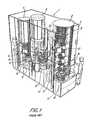
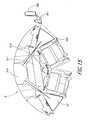
- FIG. 1is a perspective view of a 300-mm wafer processing system, constructed in accordance with the prior art.
- FIG. 2is a schematic plan view of the system of according to FIG. 1 .
- FIG. 3is a schematic plan view of a system constructed in accordance with a preferred embodiment of the invention.
- FIG. 4is a front/left/top perspective view of a Transhipment FOUP cassette, constructed in accordance with a preferred embodiment, without an open cassette.
- FIG. 5is a front/left/top perspective view of the Transhipment FOUP cassette of FIG. 4 , having an open cassette positioned therein.
- FIG. 6is a front/bottom perspective of the Transhipment FOUP cassette of FIG. 5 .
- FIG. 7Ais a schematic plan view of an input/output station of the system of FIG. 3 .
- FIG. 7Bis a schematic rear elevational view of the input/output station of the system of FIG. 3 .
- FIG. 8is a top plan view of a cassette end effector, constructed in accordance with a preferred embodiment of the present invention.
- FIG. 9is a right elevational view of the cassette end effector of FIG. 8 .
- FIG. 10is a plan top view of a cassette handler adapter, constructed in accordance with a preferred embodiment of the present invention.
- FIG. 11is a right elevational side view of the cassette handler adapter of FIG. 10 .
- FIG. 12is a top plan view of a cassette handler in engagement with the cassette handler adapter of FIGS. 10 and 11 and in engagement with a 200-mm cassette.
- FIG. 13is a right side elevational view of the cassette handler, cassette handler adapter, and 200-mm cassette of FIG. 12 .
- FIGS. 14A-14Dare top plan and rear elevational views of a platform storing cassettes.
- FIG. 15is a top plan view of the platform of FIG. 14 with a cassette sensor arrangement.
- FIG. 16Ais a top plan view of a cassette transfer platform, constructed in accordance with a preferred embodiment of the present invention
- FIG. 16Bis a front/right/top perspective view of the cassette transfer platform of FIG. 16 A.
- FIGS. 17A and 17Bare right side elevational views showing the operation of loading an open cassette into the Transhipment FOUP of the preferred embodiments.
- FIGS. 1 and 2a wafer processing system according to the prior art is described.
- the subsequent figures and corresponding text belowillustrate how the preferred embodiment is adapted to this particular wafer processing system.
- the skilled artisanwill readily appreciate, however, that the principles and advantages of the cassettes described herein can be readily adapted to other processing systems where handling of cassettes and wafers therefrom is at least partially automated.
- FIG. 1shows, diagrammatically and partially exposed, a perspective view and FIG. 2 shows a plan view of a wafer processing system for 300-mm wafers supplied 300-mm FOUP cassettes, according to the prior art.
- the wafer processing systemis indicated in its entirety by reference numeral 1 .
- This system 1comprises a housing 2 and is generally installed in a so-called “clean room.”
- partitions 3 , 4 and 5are also present.
- the housing 2delimits, with the partition 3 , a processing area or chamber 21 .
- the processing area 21comprises vertical furnaces 6 , 7 .
- the housing 2 and the partitions 3 and 4define a wafer handling chamber 22 .
- a cassette transfer chamber 23is defined between the housing 2 and partitions 4 and 5 .
- the input/output station, to transfer cassettes into and out of the system 1is indicated by reference numeral 33 .
- Wafers 13are supplied in cassettes 10 , which are placed on the input/output station 33 .
- a cassette handling device 31transfers the cassettes 10 from the input/output station 33 through a closable opening 34 into a cassette store 8 located in the cassette transfer chamber 23 .
- the cassette store 8is provided with a number of rotary platforms 27 above one another, on which the cassettes 10 are stored.
- the cassette handling device 31is movable in vertical direction by means of an elevator 35 so that the different platforms 27 can be reached.
- the cassette handling device 31is provided with a cassette end effector 32 , which has dimensions a little smaller than those of a series cut-outs 26 in the rotary platforms 27 .
- the end effector 32can be lowered through one of the cut-outs 26 in one of the platforms 27 to place the cassette on the platform 27 . Subsequently, the cassette handler 31 can be retracted from cassette store 8 .
- the cassette handling device 31is mounted such that it is able to transfer cassettes between the input/output station 33 and store 8 .
- the device 31is also capable of transferring cassettes between the store 8 and a rotatable cassette transfer platform 30 , or between the input/output station 33 and the rotatable cassette transfer platform 30 .
- the rotatable cassette transfer platform 30is constructed such that, on rotation, the cassette is placed against the partition 4 between the cassette transfer chamber 23 and the wafer handling chamber 22 .
- the partition 4is provided with a closure and a closure mechanism, together forming an interface schematically indicated by reference numeral 37 .
- the interface 37is configured for 300-mm FOUP cassettes. After placing the cassette against the interface 37 in the partition 4 , the closure mechanism grips and unlocks the closure of the FOUP cassette and simultaneously opens the closure in the partition 4 and the closure of the FOUP cassette.
- a wafer handling device 24 within the wafer handling chamber 22transfers wafers between the cassette concerned and a wafer boat 12 .
- a boat transfer arm 16moves the wafer boat 12 through a closable opening in partition 3 from the wafer handling chamber 22 into the processing chamber 21 .
- the processing chamber 21is provided with a rotary boat transfer platform 11 , supporting the wafer boat 12 .
- Two reactors, which in this case comprise furnaces 6 , 7are arranged in processing chamber 21 .
- the furnaces 6 , 7are positioned vertically and wafer boats, indicated by 12 , filled with wafers 13 , are introduced into the furnaces 6 , 7 in the vertical direction from below.
- each furnace 6 , 7has an insertion arm 14 , which is movable in the vertical direction. Only one insertion arm 14 can be seen in FIG. 1 .
- the treatment of a large number of waferscan be carried out as follows: The operator, shown diagrammatically in FIG. 1 , loads the store 8 by introducing a number of cassettes 10 on the input/output station 33 and carrying out control operations on a control panel 36 . Each of the cassettes 10 is transferred from the input/output station 33 with the aid of the cassette handling device 31 into the storage compartments 9 made for these cassettes in the store 8 , specifically on the stacked rotary platforms 27 . By rotation of the store 8 and use of the elevator 35 , it is possible to fill various compartments with the cassettes 10 . After filling the store 8 , no further human interaction is required with this automated installation.
- the cassettes 10 concernedare then removed from the store 8 by the cassette handler device 31 and placed on the cassette transfer platform 30 .
- the cassette transfer platform 30comprises two levels, schematically indicated in FIG. 1 , each level capable of receiving a FOUP cassette, where the two levels can be rotated independently of one another.
- the cassettesare placed against partition 4 .
- the wafersare removed by the wafer handler 24 and placed in a wafer boat 12 .
- the closure 19 in partition 3is opened and the wafer boat 12 is placed on the rotary boat transfer platform 11 by the boat transfer arm 16 .
- the boat transfer platform 11then moves the wafer boat 12 within the process chamber 21 to a position below the reactor to be loaded.
- the insertion mechanism or elevator 14moves the boat into the reactor 6 or 7 .
- Treated wafersexecute a movement counter to the above.
- FIG. 3shows a system according to FIGS. 1 and 2 and in addition provided with the features of the present invention.
- the system 1is provided with an input/output station 33 for receiving a cassette, which station is configured so that it can selectively receive a 300-mm FOUP cassette 212 or a 200-mm open cassette 112 .
- a cassettewhich station is configured so that it can selectively receive a 300-mm FOUP cassette 212 or a 200-mm open cassette 112 .
- no mechanical adjustmentsare required when changing from one cassette type to the other.
- the input/output station 33shown in FIG. 3 and described in more detail with respect to FIGS.
- two input/output positionsare provided in the station 33 , one configured to receive a 300-mm FOUP cassette 212 , and another configured to receive a 200-mm open cassette 112 .
- one input/output positioncan be provided that is capable of selectively receiving a 300-mm FOUP cassette or a 200-mm open cassette without requiring any mechanical adjustments.
- the system 1is provided with a cassette transfer region adjacent the input/output station 33 .
- the cassette transfer regionis defined by the transfer chamber 23 , defined by the housing 2 and partitions 4 and 5 .
- the cassette transfer regionthus includes a cassette store 8 , which can be loaded with a large number of cassettes for efficient access during processing without the need for continually retrieving cassettes from and returning cassettes to the clean room environment outside the system 1 .
- the cassette transfer regionalso houses a cassette transfer mechanism.
- the transfer mechanismincludes a cassette handler 31 and a cassette transfer platform 30 .
- the cassette handler 31includes an elevator 35 allowing access to the multiple rotary platforms 27 of the cassette store 8 , and serves to transfer cassettes among the input/output station 33 , the cassette store 8 and the cassette transfer platform 30 .
- the cassette transfer platform 30places cassettes into active communication with the interface 37 between the cassette transfer chamber 23 and the wafer handling chamber 22 , through which the wafer handling robot 24 can remove or replace wafers.
- the cassette handler 31transfers cassettes with the open side out, thus facilitating efficient storage on the round store 8 with narrow cassette ends facing the center of the rotary platforms 27 .
- the cassette transfer platform 30is therefore configured to turn cassettes received from the cassette handler 31 until the open side faces the interface 37 .
- Movements within the cassette transfer regionare controlled by a cassette handling controller, including a central processing unit (CPU) and program therefor.
- the cassette handling controllerinstructs all movement of the cassette handler 31 , rotation of the rotary platforms within the cassette store 8 , rotation of the cassette transfer platform 30 and rotation of the input/output station 33 .
- Sensors(described below) are also connected to this controller.
- the cassette handler 31 of FIGS. 1 and 2is provided with an end effector that is configured to carry the 300-mm FOUP cassettes.
- the preferred embodimentadditionally allows the end effector 32 of the cassette handler 31 to handle a 200-mm open cassette 112 .
- the preferred system 1is provided with a cassette handler adapter 400 , described in more detail below with respect to FIGS. 8-13 .
- the cassette handler adapteris designed to be fitted on the bearing surface 32 of the cassette handler 31 , to accommodate a 200-mm open cassette, and to fit into a store for this adapter plate when it is not in use.
- the cassette handling controllerinstructs the cassette handler 31 to automatically pick up the cassette handler adapter 400 from the store and, with the cassette handler adapter 400 on the bearing surface or end effector 32 of the cassette handler 31 , transfers the 200-mm cassette 112 .
- the cassette handler adapterbe mounted permanently on the cassette handler.
- the cassette handler adaptercan be slidably or rotatably mounted on the cassette handler.
- the cassette handler adaptercan, for example, be hingedly attached to the cassette handler, such that the cassette handler adapter can be flipped or otherwise adjusted between an active position for handling 200-mm open cassettes and an inactive position that allows handling of 300-mm FOUP cassettes directly upon the cassette handler.
- the preferred embodimentsalso provide structures and methods for selectively bringing either a 300-mm FOUP or a 200-mm open cassette into active connection with the wafer handling device in such a way that the sealed environments, used in a standard 300-mm FOUP approach, remain intact.
- the system 1is provided with a so-called “Transhipment FOUP” 100 designed to receive a 200-mm cassette 112 in its interior, as described in more detail below with respect to FIGS. 5 to 6 .
- the Transhipment FOUP 100is not provided with a closure.
- the critical outside dimensions of the Transhipment FOUP 100are substantially identical to those of a standard FOUP.
- the cassette handling controllerinstructs the cassette handler 31 to pick up the Transhipment FOUP 100 from its storage position and places the Transhipment FOUP on the cassette transfer platform 30 . Then the cassette handler 31 picks up the cassette handler adapter 400 ( FIGS. 8-13 ) from its storage position and, equipped with the cassette handler adapter, the cassette handler 31 picks up a 200-mm cassette 112 from a storage position. The handler 31 then transports and places the 200-mm cassette 112 in the Transhipment FOUP 100 (see FIG. 17 ).
- the Transhipment FOUP 100By rotation of cassette transfer platform 30 , the Transhipment FOUP 100 is placed against partition 4 and after opening of closure in the interface 37 , the Transhipment FOUP 100 containing the 200-mm cassette is brought into active connection with the wafer handler 24 within the handling chamber 22 . No special measures are required to allow the wafer handler 24 to handle 200-mm wafers from the 200-mm cassette. It suffices to program the wafer handler 24 with the positions of the center of the wafers and their mutual spacing, as is done for 300-mm wafer handling.
- processing chamber 21a 300-mm wafer processing furnace is provided above position 60 and a 200-mm processing furnace is provided above position 70 of the boat transfer platform or turntable 11 .
- the fact that in this case the processing chamber contains furnacesis not relevant to the invention.
- the processing areacan comprise any kind of processing tool or can comprise one or more metrology tools instead of processing tools.
- the wafer processingconsists of analysis of the wafer.
- processing chamber 21is completely absent and a wafer sorting operation forms the only “treatment” that the wafers undergo. In that case the system will comprise at least two positions where a FOUP cassette can be brought in active connection with the wafer handler 24 .
- FIGS. 4-17The Transhipment FOUP 100 for facilitating 200-mm wafer handling in the system 1 is detailed in FIGS. 4 to 6 .
- FIGS. 7A and 7Billustrate adaptations to the input/output station 33 .
- FIGS. 8 to 13illustrate the wafer handler's end effector 32 , the cassette handler adapter 400 and their interaction to receive 200-mm open cassettes 112 .
- FIGS. 14A to 15illustrate adaptations to the store 8 .
- FIGS. 16A and 16Billustrate adaptations to the rotatable cassette transfer platform 30 .
- FIG. 17illustrates placement of a 200-mm open cassette 112 within the Transhipment FOUP. Corresponding parts are indicated by like reference numerals throughout the figures.
- the Transhipment FOUPis indicated in its entirety by 100 and comprises a top plate 101 , a bottom plate 102 and sidewalls 103 .
- the sidewalls 103are provided with windows 104 .
- the front sideis provided with a flange surface 105 , adapted to be placed sealingly against partition 4 .
- the Transhipment FOUPcomprises a cassette receiving plate 110 to accommodate a 200-mm open cassette.
- the receiving plate 110is mounted on legs 111 and is provided with cassette positioning fixtures 114 to horizontally fix the 200-mm cassette on the receiving plate 110 .
- the bottom mechanical interface of the Transhipment FOUPis preferably identical to that of a standard 300-mm FOUP, at least in features relevant to interfacing with other elements of the system 1 .
- other critical outside dimensions of the Transhipment FOUP 100fall within the dimensions of the envelope of a standard FOUP cassette.
- the Transhipment FOUPis preferably also provided with a discharge pipe 121 , connected to an overpressure relief valve 120 that might become active when the Transhipment FOUP 100 is in active connection with the wafer handling chamber 22 (FIG. 3 ).
- the Transhipment FOUP 100is not provided with a closure for the open side. Despite lack of a door, because its out surfaces otherwise match those of a standard FOUP, the feature is referred to herein as a “FOUP” to distinguish the 200-mm “open” cassette.
- the Transhipment FOUP 100is shown accommodating a 200-mm “open” cassette 112 on the cassette receiving plate 110 .
- FIG. 6shows the outer surface of the bottom 102 of the Transhipment FOUP 100 with three positioning recesses 130 , intended to engage with three positioning pins, which pins are discussed below with respect to FIGS. 8 , 9 , 16 A and 16 B.
- the position and the dimensions of these recesses 130 and pinsare standardized for handling in the semiconductor industry.
- the recesses 130form elongated grooves, extending in the radial direction. The combination of the recesses 130 with the positioning pins allows the Transhipment FOUP 100 to be self-centering on the pins, similar to a standard FOUP.
- FIGS. 7A and 7Bthe preferred embodiment provides an input/output station 33 adapted to facilitate feeding 200-mm cassettes into the system 1 described above.
- FIG. 7Ais a top down view and FIG. 7B is a rear view (seen from out of the system towards the input/output station 33 ).
- the input/output station 33is provided with two cassette receiving positions 208 and 209 .
- Receiving position 209is configured to receive 300-mm FOUP cassettes 212 and position 208 is configured to receive 200-mm open cassettes 112 .
- Receiving position 209is provided with a bearing surface 201 , which can be rotated around an axis 205 to make the cassette accessible for the cassette handler 31 (FIG. 3 ).
- the bearing surface 201is provided with three positioning pins 202 , positioned and dimensioned according to SEMI STANDARD E 47.1 and the FOUP cassette is provided with matching recesses 130 (FIG. 6 ). Near each of these positioning pins 202 , a sensor 203 is provided to detect the presence of a FOUP cassette 212 .
- a plurality of positions 204are also shown in FIG. 7A to indicate the points at which the positioning pins 302 of the cassette handler 31 contact a FOUP cassette 212 when lifting the cassette from the input/output station 33 .
- the position 208 for receiving a 200-mm open cassetteis designed as a position to receive a 300-mm FOUP cassette, as described above with respect to position 209 , with an additional a load port adapter frame 210 to accommodate the 200-mm open cassette.
- the load port adapter frame 210is provided with a bottom mechanical interface identical to that of a 300-mm FOUP cassette so that it fits on the three positioning pins 202 of the 300-mm FOUP receiving position 209 . In this way, a receiving position can easily be reconfigured to the other cassette type by either removing or placing a load port adapter frame 210 from or onto a receiving position.
- the load port adapter frame 210is provided with fixtures to fix the position of the 200-mm cassette 112 and with sensors (not shown) to detect the presence of a 200-mm cassette.
- a receiving positioncan be designed such that either a 200-mm cassette or a 300-mm cassette can be received at the same position and sensors can detect whether and of what size a cassette is present.
- FIG. 8top view
- FIG. 9side view
- the end effector 32 of the cassette handler 31is shown.
- the end effectoris indicated in its entirety by reference numeral 32 and is provided with a bearing surface 301 to carry 300-mm FOUP cassettes.
- the bearing surface 301is provided with three positioning pins 302 to pick up a FOUP cassette.
- the positions of the positioning pins 302correspond to those of the positions 204 ( FIGS. 7A and 7B ) of the input/output station 33 and are shifted inwardly as compared to the positions of positioning pins 202 (FIGS. 7 A and 7 B). Both positioning pins 202 ( FIGS.
- the FOUP cassettecan be picked up by the inner positioning pins 302 on the bearing surface 301 of the cassette handler end effector 32 while it is supported by the outer positioning pins 202 of the input/output station 33 .
- the end effector bearing surface 301is provided with three sensors 303 to detect the presence of a FOUP cassette. Furthermore, the end effector bearing surface 301 is provided with a substantially rectangular hole 305 to detect the presence of a cassette handler adapter on the bearing surface 301 of the cassette handler and two substantially rectangular holes 304 for the detection of the presence of the presence of a 200-mm cassette on the cassette handler adapter, as will be explained in further detail below.
- a cassette handler adapteris provided in order to be able to handle 200-mm cassettes.
- the cassette handler adapteris indicated in its entirety by reference numeral 400 and is designed to be fitted on the bearing surface 301 of the cassette handler end effector 32 ( FIG. 8 ) and to receive a 200-mm open cassette on its bearing surface 401 .
- the cassette handler adapter 400is provided with three positioning holes 402 matching with the positioning pins 302 of the cassette handler end effector 32 .
- the cassette handler adapter 400rests by gravity on the bearing surface 301 of the cassette handler end effector 32 .
- the bearing surface 401 of the cassette handler adapter 400is provided with a bracket 405 , provided at one end with a downward pointing vane. The vane is not visible in the drawings because the cover 408 shields the position of the vane.
- the vanesticks through the rectangular hole 305 and activates a sensor mounted adjacent to the rectangular hole 305 , underneath bearing surface 301 and not shown in the drawings. In this way the presence of the cassette handler adapter 400 on the bearing surface 301 is detected.
- the cassette handle adapter 400is provided with two leaf springs 403 , fixed at one end and provided with a vane 404 at the other end.
- the upwardly pointing ends of the leaf springs 403are pressed downwards through the rectangular holes 304 .
- Adjacent to the holes 304are mounted sensors (not shown), which detect the presence of the vanes 404 and, hence, the presence of the 200-mm open cassette.
- the bearing surface 401is provided with fixtures 406 to horizontally fix the 200-mm open cassette thereon.
- the 200-mm open cassetterests by gravity on the bearing surface 401 .
- the cassette handler adapter 400is also provided with a vertical bar 407 at the open side of the cassette to prevent the wafers from shifting out of the open cassette during cassette transfer.
- the baris made of a material that does not damage or contaminate the wafers, like PEEK ®.
- a cover 408covers one end of the cassette handler adapter 400 , adjacent the vertical bar 407 .
- the cassette handler adapter 400can be stored, when not in use, at any storage location that is designed for storage of a 300-mm FOUP cassette. This can be any compartment or storage position 9 in the store 8 .
- the cassette handler adaptercan be made such that it is mounted permanently on the cassette handler, but such that it can be tilted or translated away when not is use.
- FIG. 12top view
- FIG. 13side view
- the cassette handler end effector 32is shown carrying the cassette handler adapter 400 while the cassette handler adapter 400 accommodates a 200-mm open cassette 112 .
- FIGS. 12 and 13are referenced by the same reference numerals as for corresponding parts in FIGS. 8-11 .
- the position of a wafer 13is indicated in the cassette 112 .
- FIGS. 14A to 14 Dshow a platform 27 of the store 8 from a top and side views.
- FIGS. 14A and 14Bshow a platform 27 for receiving 300-mm FOUP cassettes 212 .
- the platform 27comprises four receiving positions, each position provided with three positioning pins 502 .
- each receiving position for a 300-mm FOUP cassettecan be converted to two receiving positions for 200-mm cassettes, as shown in FIGS. 14C and 14D .
- Each position to receive a 200-mm cassetteis provided with fixtures 506 to horizontally fix the 200-mm cassette.
- the core of the rotatable store 8is provided with a clean air supply channel 510 , and filters 511 , not shown in detail, can be mounted at each 200-mm compartment of the platform 27 .
- store adapter frames 503the number of 200-mm storage locations can simply be increased or decreased by placing or removing one or more of the store adapter frames 503 .
- FIG. 15schematically shows the detection of cassettes in the cassette store 8 of FIGS. 14A-14D .
- a post 550Adjacent to the cassette store 8 , a post 550 is mounted rigidly attached to the housing and extending in the vertical direction over the entire height of the cassette store 8 .
- optical sensors 551are mounted to detect the presence or absence of a cassette.
- a reflectorInside each storage compartment, a reflector is mounted on a leaf spring. The reflector is indicated by reference numeral 552 but not shown in detail.
- the bottom of the cassettepresses downwards the leaf spring, the reflector 552 is moved out of the light beam and the emitted light is not reflected back to the sensor 551 . Consequently, the compartment is identified as being empty and available for loading a cassette only when the sensor detects a signal.
- the height of the sensors 551 on the post 550 with respect to the platform 27 and the direction in which the sensor is alignedare different for a 200-mm storage compartment as compared to a 300-mm storage compartment.
- the mounting of the post 550 , of the sensors 551 on the post 550 , and of the reflectors 552 relative to each other,are such that the presence of a cassette can be detected only when the cassette position on the rotary platform 27 is facing the cassette handler 31 (FIG. 3 ). This position, however, is the most relevant situation for detection. Although the system keeps track of where the cassettes in the system are, the sensors provide an extra check and safety in order to prevent, for example, attempts to place a cassette in a position where a cassette is already present. With this sensing strategy, each cassette position of the rotatable cassette storage platform 27 does not require an individual sensor 551 .
- FIG. 15shows also in greater detail the clean air supply channel 510 and the air filter 511 for a 200-mm compartment. Furthermore, an air guiding strip 512 , extending over substantially the entire height of the filter, is provided to guide the air in the direction of the respective centers of the 200-mm cassettes.
- FIGS. 16A and 16Bshow the rotatable cassette transfer platform 30 from top down and perspective views, respectively.
- the rotatable cassette transfer platform 30has a bearing surface 601 .
- the bearing surface 601is provided with a cutout 606 to allow vertical passage of the end effector 32 of the cassette handler 31 .
- Three positioning pins 602are positioned and sized to mate with the recesses 130 ( FIG. 6 ) in the bottom of a FOUP cassette and sensors 603 detect the presence of a FOUP cassette.
- Three sensors 603are shown in FIG. 16 A. It will be clear that this provides a high degree of redundancy and safety and that a reduced number of sensors can also be used.
- the sensors 603are not shown in FIG. 16 B.
- a sensor housing 610is mounted on the bearing surface 601 .
- the sensor housingis provided with an opening 611 to pass a detection beam from and to a sensor, which mounted inside the sensor housing and not shown in the figures.
- the sensors 603detect its presence.
- the sensors 603cannot discriminate between the presence of a standard FOUP and the Transhipment FOUP 100 .
- the sensor inside sensor housing 610is provided. The detection works similar to the detection of the presence of a cassette in the cassette store 8 , as described above.
- the sensorwill deliver a signal in the following way:
- the cassette receiving plate 110 in the Transhipment FOUP 100is provided with a reflector mounted on a leaf spring and properly positioned.
- the light emitted by the sensor in the sensor housing 610passing through hole 611 and the window 104 in wall 103 of the Transhipment FOUP that faces the sensor housing, hits the reflector.
- the reflectorreflects the light back in the direction of the sensor and the sensor within the sensor housing 610 will detect the reflected light.
- the sensorsare connected to the controller.
- a cassette handling controllercomprising a central processing unit (CPU) and associated programming.
- the controllercommunicates with the sensors described above and is programmed to have the cassette handler 31 automatically pick up (or otherwise install) the cassette handler adapter 400 when needed and to automatically store the cassette handler adapter 400 when not needed.
- the cassette handling controlleris programmed such that, when 200-mm wafers need to be handled from a 200-mm cassette, the cassette handler 31 automatically picks up the Transhipment FOUP 100 and places it on the cassette transfer platform 30 if not already there (as determined by sensor communications with the controller), and the handler 31 picks up the 200-mm open cassette and places it in the Transhipment FOUP 100 .
- the “need” for handling 200-mm open cassettes and the wafers stored thereincan be pre-programmed or can be instructed by a user at the control panel 36 (see FIG. 1 ).
- a 200-mm cassette 112is placed on the 200-mm position 208 of the receiving station 33 .
- the cassette handler controlleris programmed such that before handling the 200-mm cassette 112 , the cassette handler 31 automatically picks up the cassette handler adapter 400 from its storage position. Then the cassette handler 31 , equipped with the cassette handler adapter 400 , transfers the 200-mm cassette 112 from the receiving position 208 at the input/output station 33 to a 200-mm storage position in the cassette store 8 . Sequentially, more than one 200-mm cassette can be introduced according to the need of the moment.
- the cassette handler controllerinstructs the cassette handler 31 to transfer the Transhipment FOUP 100 from its storage position in the store 8 to the cassette transfer platform 30 .
- the cassette handler 31picks up the cassette handler adapter 400 from its storage position and, equipped with the cassette handler adapter 400 , retrieves a 200-mm cassette 112 (typically from the store 8 ) and places it on the cassette receiving plate 110 in the interior of the Transhipment FOUP 100 .
- the cassette transfer platform 30rotates the Transhipment FOUP 100 and places it against partition 4 .
- the wafer handler 24can transfer 200-mm wafers from the 200-mm open cassette 112 to a 200-mm wafer boat within the wafer handling chamber 22 for processing the wafers.
- the systemis programmed such that it will load wafers only in a wafer boat corresponding with the size of the wafers to be loaded and the wafer boat will only be loaded into a furnace or other tool corresponding to the boat size (see FIG. 3 ).
- the cassette handling controllerinstructs the cassette transfer platform to rotate the Transhipment FOUP 100 away from the interface 37 and the cassette handler 31 removes the 200-mm open cassette 112 from the Transhipment FOUP 100 , to make room for another cassette.
- FIG. 17The procedure of placing a 200-mm cassette inside a 300-mm Transhipment FOUP is illustrated in FIG. 17 .
- the cassette handler 31equipped with the cassette handler adapter 400 , and bearing a 200-mm cassette 112 , moves into the Transhipment FOUP 100 at the appropriate height.
- the cassette handler 31moves downwardly through the cut-out 113 (see FIG. 4 ) of the cassette receiving plate 110 till the 200-mm cassette 112 is placed on the cassette receiving plate 110 .
- the cassette handler 31moves downward an incremental distance to release the 200-mm cassette 112 onto the plate 110 and the cassette handler 31 retracts from the Transhipment FOUP 100 .
- the inventioncan be embodied in other ways. It is possible to replace the rotatable store by a bookshelf store wherein the compartments are arranged side-by-side according to a rectangular grid. Then the cassette handler requires corresponding degrees of freedom in movement to be able to reach all the compartments. It is also possible that the cassette handler brings the cassette in active connection with the wafer handler, with the use of a stationary platform instead of the rotatable platform according to the present embodiment.
Landscapes
- Engineering & Computer Science (AREA)
- Physics & Mathematics (AREA)
- Condensed Matter Physics & Semiconductors (AREA)
- General Physics & Mathematics (AREA)
- Manufacturing & Machinery (AREA)
- Computer Hardware Design (AREA)
- Microelectronics & Electronic Packaging (AREA)
- Power Engineering (AREA)
- Container, Conveyance, Adherence, Positioning, Of Wafer (AREA)
Abstract
Description
This application is a divisional of application Ser. No. 09/769,088, filed Jan. 24, 2001 (now U.S. Pat. No. 6,632,068, issued Oct. 14, 2003), which claims the benefit under 35 U.S.C. §119(e) of provisional Application No. 60/236,046, filed Sep. 27, 2000.
The invention relates to processing tools utilized for semiconductor wafer processing and more particularly to wafer processing tools that are configured for 300-mm wafer processing in which the wafers are supplied in FOUP cassettes.
When processing semiconductor wafers in processing tools, the processing tool is adapted to and optimized for the size of the wafer to be processed. The size of the wafers are standardized in a limited number of discrete sizes where there has been a tendency towards increasing size in the past decades in order to increase the production efficiency. The three most recently introduced wafer sizes are 150 mm, 200-mm and 300-mm diameter.
A given wafer fabrication facility will normally be configured for handling one wafer size. However, in R&D, pilot production or implementation of a new technology in production, there is a need for tools that can process multiple wafer sizes alternatingly or that can easily be reconfigured for handling different wafer sizes. In the past, when using open cassettes that hold the wafers, this was not a major issue. A wafer handling device can easily be configured so that it can handle wafers of different sizes from/to their respective open cassettes. However, the use of the closed FOUP cassettes for 300-mm wafers requires specific features in the wafer handling and cassette handling system that do not allow handling 200-mm open cassettes alternatingly in the same system.
Accordingly, a need exists for a system capable of handling multiple sizes of substrates in a state-of-the-art facility.
According to the invention a system, layed out for handling 300-mm wafers, supplied in 300-mm FOUP cassettes, is provided with a tool set to accommodate 200-mm cassettes during wafer transfer and cassette transfer. This tool set comprises a “Transhipment FOUP” cassette designed to receive a 200-mm open cassette in its interior. The term “Transhipment FOUP” is used herein as a label to distinguish 200-mm open cassettes and standard 300-mm FOUP cassettes. When 200-mm wafers need to be handled, the cassette handler places the 200-mm cassette in the Transhipment FOUP and, subsequently, the Transhipment FOUP, containing the 200-mm cassette, is brought into active connection with a wafer handling device. According to a further aspect of the invention, this tool set comprises a cassette handler adapter that allows the 300-mm FOUP cassette handler to handle 200-mm cassettes. The system is programmed such that the tools are automatically picked up from their storage position when needed.
Initially, with reference toFIGS. 1 and 2 , a wafer processing system according to the prior art is described. The subsequent figures and corresponding text below illustrate how the preferred embodiment is adapted to this particular wafer processing system. The skilled artisan will readily appreciate, however, that the principles and advantages of the cassettes described herein can be readily adapted to other processing systems where handling of cassettes and wafers therefrom is at least partially automated.
Wafers13 are supplied incassettes 10, which are placed on the input/output station 33. Acassette handling device 31 transfers thecassettes 10 from the input/output station 33 through aclosable opening 34 into acassette store 8 located in thecassette transfer chamber 23. Thecassette store 8 is provided with a number ofrotary platforms 27 above one another, on which thecassettes 10 are stored. Thecassette handling device 31 is movable in vertical direction by means of anelevator 35 so that thedifferent platforms 27 can be reached. Thecassette handling device 31 is provided with acassette end effector 32, which has dimensions a little smaller than those of a series cut-outs 26 in therotary platforms 27. When thecassette handling device 31 has transferred a cassette into thestore 8, theend effector 32 can be lowered through one of the cut-outs 26 in one of theplatforms 27 to place the cassette on theplatform 27. Subsequently, thecassette handler 31 can be retracted fromcassette store 8. Thecassette handling device 31 is mounted such that it is able to transfer cassettes between the input/output station 33 andstore 8. Thedevice 31 is also capable of transferring cassettes between thestore 8 and a rotatablecassette transfer platform 30, or between the input/output station 33 and the rotatablecassette transfer platform 30.
The rotatablecassette transfer platform 30 is constructed such that, on rotation, the cassette is placed against the partition4 between thecassette transfer chamber 23 and thewafer handling chamber 22. The partition4 is provided with a closure and a closure mechanism, together forming an interface schematically indicated byreference numeral 37. Theinterface 37 is configured for 300-mm FOUP cassettes. After placing the cassette against theinterface 37 in the partition4, the closure mechanism grips and unlocks the closure of the FOUP cassette and simultaneously opens the closure in the partition4 and the closure of the FOUP cassette.
Awafer handling device 24 within thewafer handling chamber 22 transfers wafers between the cassette concerned and awafer boat 12. After completion of the loading of wafers into thewafer boat 12, aboat transfer arm 16 moves thewafer boat 12 through a closable opening inpartition 3 from thewafer handling chamber 22 into theprocessing chamber 21. Theprocessing chamber 21 is provided with a rotaryboat transfer platform 11, supporting thewafer boat 12. Two reactors, which in this case comprise furnaces6,7, are arranged in processingchamber 21. The furnaces6,7 are positioned vertically and wafer boats, indicated by12, filled withwafers 13, are introduced into the furnaces6,7 in the vertical direction from below. To this end, each furnace6,7 has aninsertion arm 14, which is movable in the vertical direction. Only oneinsertion arm 14 can be seen in FIG.1.
The treatment of a large number of wafers can be carried out as follows: The operator, shown diagrammatically inFIG. 1 , loads thestore 8 by introducing a number ofcassettes 10 on the input/output station 33 and carrying out control operations on acontrol panel 36. Each of thecassettes 10 is transferred from the input/output station 33 with the aid of thecassette handling device 31 into thestorage compartments 9 made for these cassettes in thestore 8, specifically on thestacked rotary platforms 27. By rotation of thestore 8 and use of theelevator 35, it is possible to fill various compartments with thecassettes 10. After filling thestore 8, no further human interaction is required with this automated installation.
Thecassettes 10 concerned are then removed from thestore 8 by thecassette handler device 31 and placed on thecassette transfer platform 30. Thecassette transfer platform 30 comprises two levels, schematically indicated inFIG. 1 , each level capable of receiving a FOUP cassette, where the two levels can be rotated independently of one another. Upon rotation of thecassette transfer platform 30, the cassettes are placed against partition4. After opening of the closure of the FOUP cassette, together with theclosure 37 in partition4, the wafers are removed by thewafer handler 24 and placed in awafer boat 12. After thewafer boat 12 has been filled, and becomes available for one of the reactors6,7, theclosure 19 inpartition 3 is opened and thewafer boat 12 is placed on the rotaryboat transfer platform 11 by theboat transfer arm 16. Theboat transfer platform 11 then moves thewafer boat 12 within theprocess chamber 21 to a position below the reactor to be loaded. Then the insertion mechanism orelevator 14 moves the boat into the reactor6 or7. Treated wafers execute a movement counter to the above.
This system is described in further detail in published PCT application WO 99/38199 of applicant, the disclosure of which is incorporated herein by reference. Although an operator is described as introducing the cassette on the input/output station 33, the system is designed such that the cassettes can alternatively be introduced on the input/output station by means of an automatic guided vehicle (AGV) or by an overhead hoist system. In such a case, the control system of the wafer processing system can be connected to a host computer system that carries out the control functions. In this way, no human interaction at the wafer processing system is required at all.
Further, the system1 is provided with a cassette transfer region adjacent the input/output station 33. In the illustrated embodiment, the cassette transfer region is defined by thetransfer chamber 23, defined by thehousing 2 andpartitions 4 and5. The cassette transfer region thus includes acassette store 8, which can be loaded with a large number of cassettes for efficient access during processing without the need for continually retrieving cassettes from and returning cassettes to the clean room environment outside the system1.
The cassette transfer region also houses a cassette transfer mechanism. In the illustrated embodiment, the transfer mechanism includes acassette handler 31 and acassette transfer platform 30. Thecassette handler 31 includes anelevator 35 allowing access to the multiplerotary platforms 27 of thecassette store 8, and serves to transfer cassettes among the input/output station 33, thecassette store 8 and thecassette transfer platform 30. Thecassette transfer platform 30, in turn, places cassettes into active communication with theinterface 37 between thecassette transfer chamber 23 and thewafer handling chamber 22, through which thewafer handling robot 24 can remove or replace wafers. In the illustrated embodiment, thecassette handler 31 transfers cassettes with the open side out, thus facilitating efficient storage on theround store 8 with narrow cassette ends facing the center of therotary platforms 27. Thecassette transfer platform 30 is therefore configured to turn cassettes received from thecassette handler 31 until the open side faces theinterface 37.
Movements within the cassette transfer region are controlled by a cassette handling controller, including a central processing unit (CPU) and program therefor. In particular, the cassette handling controller instructs all movement of thecassette handler 31, rotation of the rotary platforms within thecassette store 8, rotation of thecassette transfer platform 30 and rotation of the input/output station 33. Sensors (described below) are also connected to this controller.
Thecassette handler 31 ofFIGS. 1 and 2 is provided with an end effector that is configured to carry the 300-mm FOUP cassettes. The preferred embodiment additionally allows theend effector 32 of thecassette handler 31 to handle a 200-mmopen cassette 112. For this purpose, the preferred system1 is provided with acassette handler adapter 400, described in more detail below with respect toFIGS. 8-13 . The cassette handler adapter is designed to be fitted on the bearingsurface 32 of thecassette handler 31, to accommodate a 200-mm open cassette, and to fit into a store for this adapter plate when it is not in use.
When a 200-mmopen cassette 112 is to be handled, the cassette handling controller instructs thecassette handler 31 to automatically pick up thecassette handler adapter 400 from the store and, with thecassette handler adapter 400 on the bearing surface orend effector 32 of thecassette handler 31, transfers the 200-mm cassette 112. Instead of storing the cassette handler adapter at a storing or parking location, it is also possible that the cassette handler adapter be mounted permanently on the cassette handler. As a third option, the cassette handler adapter can be slidably or rotatably mounted on the cassette handler. In this third alternative, the cassette handler adapter can, for example, be hingedly attached to the cassette handler, such that the cassette handler adapter can be flipped or otherwise adjusted between an active position for handling 200-mm open cassettes and an inactive position that allows handling of 300-mm FOUP cassettes directly upon the cassette handler.
The preferred embodiments also provide structures and methods for selectively bringing either a 300-mm FOUP or a 200-mm open cassette into active connection with the wafer handling device in such a way that the sealed environments, used in a standard 300-mm FOUP approach, remain intact. For this purpose, the system1 is provided with a so-called “Transhipment FOUP”100 designed to receive a 200-mm cassette 112 in its interior, as described in more detail below with respect toFIGS. 5 to6. Unlike standard FOUPs, theTranshipment FOUP 100 is not provided with a closure. The critical outside dimensions of theTranshipment FOUP 100 are substantially identical to those of a standard FOUP.
When 200-mm wafers need to be handled, the cassette handling controller instructs thecassette handler 31 to pick up theTranshipment FOUP 100 from its storage position and places the Transhipment FOUP on thecassette transfer platform 30. Then thecassette handler 31 picks up the cassette handler adapter400 (FIGS. 8-13 ) from its storage position and, equipped with the cassette handler adapter, thecassette handler 31 picks up a 200-mm cassette 112 from a storage position. Thehandler 31 then transports and places the 200-mm cassette 112 in the Transhipment FOUP100 (see FIG.17). By rotation ofcassette transfer platform 30, theTranshipment FOUP 100 is placed against partition4 and after opening of closure in theinterface 37, theTranshipment FOUP 100 containing the 200-mm cassette is brought into active connection with thewafer handler 24 within the handlingchamber 22. No special measures are required to allow thewafer handler 24 to handle 200-mm wafers from the 200-mm cassette. It suffices to program thewafer handler 24 with the positions of the center of the wafers and their mutual spacing, as is done for 300-mm wafer handling.
Inprocessing chamber 21, a 300-mm wafer processing furnace is provided aboveposition 60 and a 200-mm processing furnace is provided aboveposition 70 of the boat transfer platform orturntable 11. The fact that in this case the processing chamber contains furnaces is not relevant to the invention. The processing area can comprise any kind of processing tool or can comprise one or more metrology tools instead of processing tools. In the latter case, the wafer processing consists of analysis of the wafer. It is also possible that processingchamber 21 is completely absent and a wafer sorting operation forms the only “treatment” that the wafers undergo. In that case the system will comprise at least two positions where a FOUP cassette can be brought in active connection with thewafer handler 24.
The invention will be explained in further detail below referring toFIGS. 4-17 . TheTranshipment FOUP 100 for facilitating 200-mm wafer handling in the system1 is detailed inFIGS. 4 to6.FIGS. 7A and 7B illustrate adaptations to the input/output station 33.FIGS. 8 to13 illustrate the wafer handler'send effector 32, thecassette handler adapter 400 and their interaction to receive 200-mmopen cassettes 112.FIGS. 14A to15 illustrate adaptations to thestore 8.FIGS. 16A and 16B illustrate adaptations to the rotatablecassette transfer platform 30.FIG. 17 illustrates placement of a 200-mmopen cassette 112 within the Transhipment FOUP. Corresponding parts are indicated by like reference numerals throughout the figures.
InFIG. 4 , showing in perspective view a Transhipment FOUP without a 200-mm open cassette, the Transhipment FOUP is indicated in its entirety by 100 and comprises atop plate 101, abottom plate 102 andsidewalls 103. Thesidewalls 103 are provided withwindows 104. The front side is provided with aflange surface 105, adapted to be placed sealingly against partition4. In its interior, the Transhipment FOUP comprises acassette receiving plate 110 to accommodate a 200-mm open cassette. The receivingplate 110 is mounted onlegs 111 and is provided withcassette positioning fixtures 114 to horizontally fix the 200-mm cassette on the receivingplate 110. The bottom mechanical interface of the Transhipment FOUP is preferably identical to that of a standard 300-mm FOUP, at least in features relevant to interfacing with other elements of the system1. Similarly, other critical outside dimensions of theTranshipment FOUP 100 fall within the dimensions of the envelope of a standard FOUP cassette.
The Transhipment FOUP is preferably also provided with adischarge pipe 121, connected to anoverpressure relief valve 120 that might become active when theTranshipment FOUP 100 is in active connection with the wafer handling chamber22 (FIG.3). TheTranshipment FOUP 100 is not provided with a closure for the open side. Despite lack of a door, because its out surfaces otherwise match those of a standard FOUP, the feature is referred to herein as a “FOUP” to distinguish the 200-mm “open” cassette.
With reference toFIG. 5 , theTranshipment FOUP 100 is shown accommodating a 200-mm “open”cassette 112 on thecassette receiving plate 110.FIG. 6 shows the outer surface of the bottom102 of theTranshipment FOUP 100 with three positioningrecesses 130, intended to engage with three positioning pins, which pins are discussed below with respect toFIGS. 8 ,9,16A and16B. The position and the dimensions of theserecesses 130 and pins are standardized for handling in the semiconductor industry. Therecesses 130 form elongated grooves, extending in the radial direction. The combination of therecesses 130 with the positioning pins allows theTranshipment FOUP 100 to be self-centering on the pins, similar to a standard FOUP.
With reference toFIGS. 7A and 7B , the preferred embodiment provides an input/output station 33 adapted to facilitate feeding 200-mm cassettes into the system1 described above.FIG. 7A is a top down view andFIG. 7B is a rear view (seen from out of the system towards the input/output station33). The input/output station 33 is provided with twocassette receiving positions position 209 is configured to receive 300-mm FOUP cassettes 212 andposition 208 is configured to receive 200-mmopen cassettes 112.
Receivingposition 209 is provided with abearing surface 201, which can be rotated around anaxis 205 to make the cassette accessible for the cassette handler31 (FIG.3). The bearingsurface 201 is provided with three positioningpins 202, positioned and dimensioned according to SEMI STANDARD E 47.1 and the FOUP cassette is provided with matching recesses130 (FIG.6). Near each of these positioningpins 202, asensor 203 is provided to detect the presence of aFOUP cassette 212. A plurality ofpositions 204 are also shown inFIG. 7A to indicate the points at which the positioning pins302 of thecassette handler 31 contact aFOUP cassette 212 when lifting the cassette from the input/output station 33.
Theposition 208 for receiving a 200-mm open cassette is designed as a position to receive a 300-mm FOUP cassette, as described above with respect toposition 209, with an additional a loadport adapter frame 210 to accommodate the 200-mm open cassette. The loadport adapter frame 210 is provided with a bottom mechanical interface identical to that of a 300-mm FOUP cassette so that it fits on the threepositioning pins 202 of the 300-mmFOUP receiving position 209. In this way, a receiving position can easily be reconfigured to the other cassette type by either removing or placing a loadport adapter frame 210 from or onto a receiving position. The loadport adapter frame 210 is provided with fixtures to fix the position of the 200-mm cassette 112 and with sensors (not shown) to detect the presence of a 200-mm cassette. In an alternative embodiment, a receiving position can be designed such that either a 200-mm cassette or a 300-mm cassette can be received at the same position and sensors can detect whether and of what size a cassette is present.
With reference toFIG. 8 (top view) andFIG. 9 (side view), theend effector 32 of thecassette handler 31 is shown. The end effector is indicated in its entirety byreference numeral 32 and is provided with abearing surface 301 to carry 300-mm FOUP cassettes. The bearingsurface 301 is provided with three positioningpins 302 to pick up a FOUP cassette. The positions of the positioning pins302 correspond to those of the positions204 (FIGS. 7A and 7B ) of the input/output station 33 and are shifted inwardly as compared to the positions of positioning pins202 (FIGS.7A and7B). Both positioning pins202 (FIGS. 7A and 7B ) and302 can be accommodated in the positioning recesses130 in thebottom plate 102 of the FOUP cassette because theserecesses 130 extend over some distance in the radial direction. In this way, the FOUP cassette can be picked up by the inner positioning pins302 on thebearing surface 301 of the cassettehandler end effector 32 while it is supported by the outer positioning pins202 of the input/output station 33.
The endeffector bearing surface 301 is provided with threesensors 303 to detect the presence of a FOUP cassette. Furthermore, the endeffector bearing surface 301 is provided with a substantiallyrectangular hole 305 to detect the presence of a cassette handler adapter on thebearing surface 301 of the cassette handler and two substantiallyrectangular holes 304 for the detection of the presence of the presence of a 200-mm cassette on the cassette handler adapter, as will be explained in further detail below.
With reference toFIG. 10 (top view) andFIG. 11 (side view), a cassette handler adapter is provided in order to be able to handle 200-mm cassettes. The cassette handler adapter is indicated in its entirety byreference numeral 400 and is designed to be fitted on thebearing surface 301 of the cassette handler end effector32 (FIG. 8 ) and to receive a 200-mm open cassette on itsbearing surface 401. For this purpose thecassette handler adapter 400 is provided with threepositioning holes 402 matching with the positioning pins302 of the cassettehandler end effector 32. Thecassette handler adapter 400 rests by gravity on thebearing surface 301 of the cassettehandler end effector 32.
When thecassette handler adapter 400 is placed on the cassettehandler end effector 32,sensors 303 are activated and the presence of an object on the bearing surface is detected. However, thesensors 303 cannot discriminate between the presence of a FOUP cassette and the presence of acassette handler adapter 400. To allow the unambiguous determination of the presence of thecassette handler adapter 400, the bearingsurface 401 of thecassette handler adapter 400 is provided with abracket 405, provided at one end with a downward pointing vane. The vane is not visible in the drawings because thecover 408 shields the position of the vane. When thecassette handler adapter 400 is placed on thebearing surface 301 of the cassettehandler end effector 32, the vane sticks through therectangular hole 305 and activates a sensor mounted adjacent to therectangular hole 305, underneath bearingsurface 301 and not shown in the drawings. In this way the presence of thecassette handler adapter 400 on thebearing surface 301 is detected.
Furthermore, thecassette handle adapter 400 is provided with twoleaf springs 403, fixed at one end and provided with avane 404 at the other end. When a 200-mm open cassette is placed on thebearing surface 401 of thecassette handler adapter 400, the upwardly pointing ends of theleaf springs 403, provided with thevanes 404, are pressed downwards through therectangular holes 304. Adjacent to theholes 304 are mounted sensors (not shown), which detect the presence of thevanes 404 and, hence, the presence of the 200-mm open cassette.
Furthermore, the bearingsurface 401 is provided withfixtures 406 to horizontally fix the 200-mm open cassette thereon. The 200-mm open cassette rests by gravity on thebearing surface 401. Thecassette handler adapter 400 is also provided with avertical bar 407 at the open side of the cassette to prevent the wafers from shifting out of the open cassette during cassette transfer. The bar is made of a material that does not damage or contaminate the wafers, like PEEK ®. Acover 408 covers one end of thecassette handler adapter 400, adjacent thevertical bar 407.
Thecassette handler adapter 400, with a bottom mechanical interface identical to that of a 300-mm FOUP cassette, can be stored, when not in use, at any storage location that is designed for storage of a 300-mm FOUP cassette. This can be any compartment orstorage position 9 in thestore 8. In an alternative design, not shown in further detail, the cassette handler adapter can be made such that it is mounted permanently on the cassette handler, but such that it can be tilted or translated away when not is use.
InFIG. 12 (top view) andFIG. 13 (side view) the cassettehandler end effector 32 is shown carrying thecassette handler adapter 400 while thecassette handler adapter 400 accommodates a 200-mmopen cassette 112. Features inFIGS. 12 and 13 are referenced by the same reference numerals as for corresponding parts inFIGS. 8-11 . The position of awafer 13 is indicated in thecassette 112.
In thestore 8 for cassettes, a number of storage positions for 300-mm FOUP cassettes are similarly converted to 200-mm storage positions.FIGS. 14A to14D show aplatform 27 of thestore 8 from a top and side views.FIGS. 14A and 14B show aplatform 27 for receiving 300-mm FOUP cassettes 212. Theplatform 27 comprises four receiving positions, each position provided with three positioning pins502. In the preferred embodiment, each receiving position for a 300-mm FOUP cassette can be converted to two receiving positions for 200-mm cassettes, as shown inFIGS. 14C and 14D . This can be achieved by providing a receiving position for a 300-mm FOUP cassette with astore adapter frame 503, designed to fit on the 3 positioning pins502 and to receive two 200-mm cassettes on its upper surface. Each position to receive a 200-mm cassette is provided withfixtures 506 to horizontally fix the 200-mm cassette. The core of therotatable store 8 is provided with a cleanair supply channel 510, and filters511, not shown in detail, can be mounted at each 200-mm compartment of theplatform 27. By the use of store adapter frames503, the number of 200-mm storage locations can simply be increased or decreased by placing or removing one or more of the store adapter frames503.
On the other hand, in case of a Transhipment FOUP100 (FIGS. 4-6 ) the sensor will deliver a signal in the following way: Thecassette receiving plate 110 in theTranshipment FOUP 100 is provided with a reflector mounted on a leaf spring and properly positioned. When anempty Transhipment FOUP 100 is placed on thecassette transfer platform 30, the light emitted by the sensor in thesensor housing 610, passing throughhole 611 and thewindow 104 inwall 103 of the Transhipment FOUP that faces the sensor housing, hits the reflector. The reflector reflects the light back in the direction of the sensor and the sensor within thesensor housing 610 will detect the reflected light. The sensors are connected to the controller. Whensensors 603 and the sensor inside thesensor housing 610 are simultaneously activated, the presence of theTranshipment FOUP 100 on theplatform 30 is unambiguously detected. When a 200-mm open cassette is subsequently placed on thecassette receiving plate 110 of the Transhipment FOUP, the leaf spring is pressed downwards and the reflector, mounted on the leaf spring, is moved out of the beam and the sensor does not detect a signal anymore. By this sequence of events the presence of a 200-mm cassette 112 inside theTranshipment FOUP 100 is detected. As can be seen fromFIG. 16A , the position of the cassette on theplatform 30 is somewhat asymmetrical.
As noted above, movements within the cassette transfer region are controlled by a cassette handling controller, comprising a central processing unit (CPU) and associated programming. The controller communicates with the sensors described above and is programmed to have thecassette handler 31 automatically pick up (or otherwise install) thecassette handler adapter 400 when needed and to automatically store thecassette handler adapter 400 when not needed. Similarly, the cassette handling controller is programmed such that, when 200-mm wafers need to be handled from a 200-mm cassette, thecassette handler 31 automatically picks up theTranshipment FOUP 100 and places it on thecassette transfer platform 30 if not already there (as determined by sensor communications with the controller), and thehandler 31 picks up the 200-mm open cassette and places it in theTranshipment FOUP 100. The “need” for handling 200-mm open cassettes and the wafers stored therein can be pre-programmed or can be instructed by a user at the control panel36 (see FIG.1).
In operation, when one or more 200-mmopen cassettes 112 need to be introduced into the system1 the procedure is as follows: a 200-mm cassette 112 is placed on the 200-mm position 208 of the receivingstation 33. When the system1 is instructed to handle the 200-mm cassette 112, the cassette handler controller is programmed such that before handling the 200-mm cassette 112, thecassette handler 31 automatically picks up thecassette handler adapter 400 from its storage position. Then thecassette handler 31, equipped with thecassette handler adapter 400, transfers the 200-mm cassette 112 from the receivingposition 208 at the input/output station 33 to a 200-mm storage position in thecassette store 8. Sequentially, more than one 200-mm cassette can be introduced according to the need of the moment.
When 200-mm wafers need to be loaded into aboat 12, the cassette handler controller instructs thecassette handler 31 to transfer theTranshipment FOUP 100 from its storage position in thestore 8 to thecassette transfer platform 30. Then, thecassette handler 31 picks up thecassette handler adapter 400 from its storage position and, equipped with thecassette handler adapter 400, retrieves a 200-mm cassette112 (typically from the store8) and places it on thecassette receiving plate 110 in the interior of theTranshipment FOUP 100. Then thecassette transfer platform 30 rotates theTranshipment FOUP 100 and places it against partition4. After opening the closure of theinterface 37 in partition4, thewafer handler 24 can transfer 200-mm wafers from the 200-mmopen cassette 112 to a 200-mm wafer boat within thewafer handling chamber 22 for processing the wafers. The system is programmed such that it will load wafers only in a wafer boat corresponding with the size of the wafers to be loaded and the wafer boat will only be loaded into a furnace or other tool corresponding to the boat size (see FIG.3). When transfer of the 200-mm wafers out of thecassette 112 is complete, the cassette handling controller instructs the cassette transfer platform to rotate theTranshipment FOUP 100 away from theinterface 37 and thecassette handler 31 removes the 200-mmopen cassette 112 from theTranshipment FOUP 100, to make room for another cassette.
The procedure of placing a 200-mm cassette inside a 300-mm Transhipment FOUP is illustrated in FIG.17. Thecassette handler 31, equipped with thecassette handler adapter 400, and bearing a 200-mm cassette 112, moves into theTranshipment FOUP 100 at the appropriate height. When thecassette handler 31 has reached the correct distance into theTranshipment FOUP 100, thecassette handler 31 moves downwardly through the cut-out113 (seeFIG. 4 ) of thecassette receiving plate 110 till the 200-mm cassette 112 is placed on thecassette receiving plate 110. Then thecassette handler 31 moves downward an incremental distance to release the 200-mm cassette 112 onto theplate 110 and thecassette handler 31 retracts from theTranshipment FOUP 100.
To someone skilled in the art, it will be clear that the invention can be embodied in other ways. It is possible to replace the rotatable store by a bookshelf store wherein the compartments are arranged side-by-side according to a rectangular grid. Then the cassette handler requires corresponding degrees of freedom in movement to be able to reach all the compartments. It is also possible that the cassette handler brings the cassette in active connection with the wafer handler, with the use of a stationary platform instead of the rotatable platform according to the present embodiment.
The skilled artisan will similarly appreciate that many other omissions, additions and modifications to the preferred embodiment can be made without departing from the spirit and scope of the present invention. It is accordingly desired that the present embodiment be considered in all respects as illustrative and not restrictive, reference being made to the appended claims rather than to the foregoing description to indicate the scope of the invention.
Claims (21)
1. A wafer processing system configured for handling standard 300-mm FOUP cassettes, the system comprising:
an input/output station;
a cassette transfer region adjacent to the input/output station;
a wafer handling chamber adjacent to the cassette transfer region, the wafer handling chamber senarated from the cassette transfer region by an interface configured for interacting with a 300-mm FOUP cassette;
a cassette transfer mechanism configured for transferring cassettes from the input/output station through the cassette transfer region to the interface;
a wafer handling robot within the wafer handling chamber, the wafer handling robot configured to access wafers within cassettes through the interface; and
a tool set adapted for receiving and transferring 200-mm open cassettes within the wafer processing system, wherein the cassette transfer mechanism comprises a cassette handler robot configured to transfer cassettes between the input/output station and the cassette transfer region, wherein the cassette handler robot has a bearing surface designed to receive a standard 300-mm FOUP cassette, the wafer processing system further comprising a cassette handler adapter configured to fit on the bearing surface, the cassette handler adapter further configured to accommodate a 200-mm open cassette thereon.
2. The wafer processing system ofclaim 1 , wherein the interface comprises a partition between the cassette transfer region and the wafer handling chamber, the partition having a closable opening therein mating with a 300-mm FOUP cassette.
3. The wafer processing system ofclaim 1 , wherein the tool set comprises a Transhipment FOUP cassette having external surfaces conforming to a 300-mm FOUP cassette standard, the Transhipment FOUP cassette comprising an internal platform configured to receive a 200-mm open cassette.
4. The wafer processing system ofclaim 3 , further comprising a storage position within the cassette transfer region to store the Transhipment FOUP cassette when not in use.
5. The wafer processing system ofclaim 3 , further comprising a sensor arrangement to determine presence of a 200-mm cassette at discrete positions within the wafer processing system, the sensor arrangement capable of distinguishing presence of a 300-mm FOUP cassette from presence of a 200-mm open cassette at the discrete locations.
6. The wafer processing system ofclaim 5 , wherein the sensor arrangement is capable of distinguishing presence of a standard 300-mm FOUP cassette from presence of the Transhipment FOUP cassette at a discrete location.
7. The wafer processing system ofclaim 5 , wherein the sensor arrangement includes a plurality of light sensors, light emitters, reflectors and a central processing unit.
8. The wafer processing system ofclaim 1 , wherein the cassette transfer mechanism further comprises a cassette transfer platform configured to receive cassettes from the cassette handler robot and place cassettes into an active position accessible by the wafer transfer robot through the interface.
9. The wafer processing system ofclaim 8 , wherein the cassette transfer platform comprises a turntable.
10. The wafer processing system ofclaim 1 , further comprising a storage position to store the cassette handler adapter when not in use.
11. The wafer processing system ofclaim 10 , wherein the storage position is on the cassette handler robot.
12. The wafer processing system ofclaim 10 , further comprising a cassette store accessible to the cassette handler robot, the storage position for storing the cassette handler adapter comprising a designated position within the cassette store.
13. The wafer processing system ofclaim 1 , further comprising a cassette store within the cassette transfer region, the cassette store accessible to the cassette handler robot, the cassette store comprising a storage platform having a plurality of 300-mm FOUP store positions.
14. The wafer processing system ofclaim 13 , wherein the store comprises a plurality of stacked rotary storage platforms, each platform divided into a plurality of storage compartments and defining the 300-mm FOUP store positions.
15. A wafer processing system configured for handling standard 300-mm FOUP cassettes, the system comprising:
an input/output station;
a cassette transfer region adjacent to the input/output station;
a wafer handling chamber adjacent to the cassette transfer region, the wafer handling chamber separated from the cassette transfer region by an interface configured for interacting with a 300-mm FOUP cassette;
a cassette transfer mechanism configured for transferring cassettes from the input/output station through the cassette transfer region to the interface;
a wafer handling robot within the wafer handling chamber, the wafer handling robot configured to access wafers within cassettes through the interface; and
a tool set adapted for receiving and transferring 200-mm open cassettes within the wafer processing system, wherein the cassette transfer mechanism comprises a cassette handler robot configured to transfer cassettes between the input/output station and the cassette transfer region, further comprising a cassette store within the cassette transfer region, the cassette store accessible to the cassette handler robot, the cassette store comprising a storage platform having a plurality of 300-mm FOUP store positions, wherein the tool set comprises a store accommodation plate, configured to fit on one of the 300-mm FOUP store positions, the store accommodation plate configured to accommodate at least one 200-mm open cassette.
16. The wafer processing system ofclaim 15 , wherein the store accommodation plate is configured to accommodate two 200-mm open cassettes.
17. A wafer processing system configured for handling standard 300-mm FOUP cassettes, the system comprising:
an input/output station;
a cassette transfer region adjacent to the input/output station;
a wafer handling chamber adjacent to the cassette transfer region, the wafer handling chamber separated from the cassette transfer region by an interface configured for interacting with a 300-mm FOUP cassette;
a cassette transfer mechanism configured for transferring cassettes from the input/output station through the cassette transfer region to the interface;
a wafer handling robot within the wafer handling chamber, the wafer handling robot configured to access wafers within cassettes through the interface; and
a tool set adapted for receiving and transferring 200-mm open cassettes within the wafer processing system, wherein the tool set comprises a load port adapter plate configured to fit on a position of the input/output station designed to receive a standard 300-mm FOUP cassette, the load port adapter plate configured to accommodate a 200-mm open cassette thereon.
18. A wafer processing system configured for handling standard 300-mm FOUP cassettes, the system comprising:
an input/output station;
a cassette transfer region adjacent to the input/output station;
a wafer handling chamber adjacent to the cassette transfer region, the wafer handling chamber separated from the cassette transfer region by an interface configured for interacting with a 300-mm FOUP cassette;
a cassette transfer mechanism configured for transferring cassettes from the input/output station through the cassette transfer region to the interface;
a wafer handling robot within the wafer handling chamber, the wafer handling robot configured to access wafers within cassettes through the interface; and
a tool set adapted for receiving and transferring 200-mm open cassettes within the wafer processing system, wherein the cassette transfer mechanism comprises a cassette handler robot configured to transfer cassettes between the input/output station and the cassette transfer region, wherein the tool set comprises a Transhipment FOUP cassette having external surfaces conforming to a 300-mm FOUP cassette standard, the Transhipment FOUP cassette comprising an internal platform configured to receive a 200-mm open cassette, further comprising a sensor arrangement to determine presence of a 200-mm cassette at discrete positions within the wafer processing system, the sensor arrangement capable of distinguishing presence of a 300-mm FOUP cassette from presence of a 200-mm open cassette at the discrete locations, wherein the sensor arrangement includes a plurality of light sensors, light emitters, reflectors and a central processing unit, wherein the cassette handler robot includes an end effector with a bearing surface configured to receive a standard 300-mm FOUP cassette, the wafer processing system further comprising a cassette handler adapter configured to fit on the bearing surface of the cassette handler robot, the cassette handler adapter further configured to accommodate a 200-mm open cassette thereon, wherein the sensor arrangement comprises at least one light sensor and one light emitter arranged to detect the cassette handler adapter when mounted upon the bearing surface of the cassette handler robot.
19. The wafer processing system ofclaim 18 , wherein the sensors communicate with the central processing unit and the central processing unit is provided with a program instructing the cassette handler robot to automatically pick up the cassette handler adapter when needed for transferring a 200-mm open cassette, the program further instructing the cassette handler robot to store the cassette handler adapter when not needed for transferring a 200-mm open cassette.
20. The wafer processing system ofclaim 18 , wherein the sensors communicate with the central processing unit and the central processing unit is provided with a program instructing the cassette handler robot to automatically place a 200-mm open cassette inside the Transhipment FOUP when wafers need to be transferred from the 200-mm open cassette to the wafer transfer robot or vice versa, the program further instructing the cassette handler robot to remove the 200-mm open cassette when transfer of wafers between the 200-mm open cassette and the wafer handler robot is complete.
21. The wafer processing system ofclaim 18 , wherein
the bearing surface of the cassette handler robot has at least one sensor hole,
the cassette handler adapter includes a depending vane aligned with the sensor hole when the cassette handler adapter is mounted upon the bearing surface of the cassette handler robot, and
the sensor arrangement includes a sensor for detecting the vane extending downwardly through the sensor hole when the cassette handler adapter is mounted upon the bearing surface of the cassette handler robot.
Priority Applications (1)
| Application Number | Priority Date | Filing Date | Title |
|---|---|---|---|
| US10/641,807US6981832B2 (en) | 2000-09-27 | 2003-08-15 | Wafer handling system |
Applications Claiming Priority (3)
| Application Number | Priority Date | Filing Date | Title |
|---|---|---|---|
| US23604600P | 2000-09-27 | 2000-09-27 | |
| US09/769,088US6632068B2 (en) | 2000-09-27 | 2001-01-24 | Wafer handling system |
| US10/641,807US6981832B2 (en) | 2000-09-27 | 2003-08-15 | Wafer handling system |
Related Parent Applications (1)
| Application Number | Title | Priority Date | Filing Date |
|---|---|---|---|
| US09/769,088DivisionUS6632068B2 (en) | 2000-09-27 | 2001-01-24 | Wafer handling system |
Publications (2)
| Publication Number | Publication Date |
|---|---|
| US20040037675A1 US20040037675A1 (en) | 2004-02-26 |
| US6981832B2true US6981832B2 (en) | 2006-01-03 |
Family
ID=26929406
Family Applications (2)
| Application Number | Title | Priority Date | Filing Date |
|---|---|---|---|
| US09/769,088Expired - Fee RelatedUS6632068B2 (en) | 2000-09-27 | 2001-01-24 | Wafer handling system |
| US10/641,807Expired - Fee RelatedUS6981832B2 (en) | 2000-09-27 | 2003-08-15 | Wafer handling system |
Family Applications Before (1)
| Application Number | Title | Priority Date | Filing Date |
|---|---|---|---|
| US09/769,088Expired - Fee RelatedUS6632068B2 (en) | 2000-09-27 | 2001-01-24 | Wafer handling system |
Country Status (4)
| Country | Link |
|---|---|
| US (2) | US6632068B2 (en) |
| EP (2) | EP1197990A3 (en) |
| JP (1) | JP2002151565A (en) |
| KR (1) | KR100648238B1 (en) |
Cited By (364)
| Publication number | Priority date | Publication date | Assignee | Title |
|---|---|---|---|---|
| US20060045662A1 (en)* | 2004-07-29 | 2006-03-02 | Kla Tencor, Inc. | Quick swap load port |
| US20070264104A1 (en)* | 2006-05-11 | 2007-11-15 | Tokyo Electron Limited | Processing apparatus |
| US20080031708A1 (en)* | 2006-07-10 | 2008-02-07 | Bonora Anthony C | Variable lot size load port |
| US20080226428A1 (en)* | 2007-03-16 | 2008-09-18 | Ravinder Aggarwal | Substrate handling chamber with movable substrate carrier loading platform |
| US20090003825A1 (en)* | 2007-06-29 | 2009-01-01 | Tokyo Electron Limited | Substrate processing system |
| US7604449B1 (en)* | 2005-06-27 | 2009-10-20 | Kla-Tencor Technologies Corporation | Equipment front end module |
| US20090267626A1 (en)* | 2006-05-11 | 2009-10-29 | Tokyo Electron Limited | Probing apparatus and probing method |
| US7740437B2 (en) | 2006-09-22 | 2010-06-22 | Asm International N.V. | Processing system with increased cassette storage capacity |
| US20110005966A1 (en)* | 2009-07-10 | 2011-01-13 | Ming-Chien Chiu | Foup and robotic flange thereof |
| US20120213613A1 (en)* | 2011-02-18 | 2012-08-23 | De Ridder Chris G M | Wafer boat assembly, loading apparatus comprising such a wafer boat assembly and method for loading a vertical furnace |
| US20130000254A1 (en)* | 2011-06-28 | 2013-01-03 | Dynamic Micro Systems, Semiconductor Equipment Gmbh | Semiconductor stocker systems and methods |
| US20130001846A1 (en)* | 2010-01-22 | 2013-01-03 | Lg Siltron Incorporated | Cassette jig for wafer cleaning apparatus and cassette assembly having the same |
| US20140308108A1 (en)* | 2013-04-10 | 2014-10-16 | Globalfoundries Inc. | System for separately handling different size foups |
| US10229833B2 (en) | 2016-11-01 | 2019-03-12 | Asm Ip Holding B.V. | Methods for forming a transition metal nitride film on a substrate by atomic layer deposition and related semiconductor device structures |
| US10249577B2 (en) | 2016-05-17 | 2019-04-02 | Asm Ip Holding B.V. | Method of forming metal interconnection and method of fabricating semiconductor apparatus using the method |
| US10249524B2 (en) | 2017-08-09 | 2019-04-02 | Asm Ip Holding B.V. | Cassette holder assembly for a substrate cassette and holding member for use in such assembly |
| US10262859B2 (en) | 2016-03-24 | 2019-04-16 | Asm Ip Holding B.V. | Process for forming a film on a substrate using multi-port injection assemblies |
| US10269558B2 (en) | 2016-12-22 | 2019-04-23 | Asm Ip Holding B.V. | Method of forming a structure on a substrate |
| US10276355B2 (en) | 2015-03-12 | 2019-04-30 | Asm Ip Holding B.V. | Multi-zone reactor, system including the reactor, and method of using the same |
| US10283353B2 (en) | 2017-03-29 | 2019-05-07 | Asm Ip Holding B.V. | Method of reforming insulating film deposited on substrate with recess pattern |
| US10290508B1 (en) | 2017-12-05 | 2019-05-14 | Asm Ip Holding B.V. | Method for forming vertical spacers for spacer-defined patterning |
| US10312055B2 (en) | 2017-07-26 | 2019-06-04 | Asm Ip Holding B.V. | Method of depositing film by PEALD using negative bias |
| US10312129B2 (en) | 2015-09-29 | 2019-06-04 | Asm Ip Holding B.V. | Variable adjustment for precise matching of multiple chamber cavity housings |
| US10319588B2 (en) | 2017-10-10 | 2019-06-11 | Asm Ip Holding B.V. | Method for depositing a metal chalcogenide on a substrate by cyclical deposition |
| US10322384B2 (en) | 2015-11-09 | 2019-06-18 | Asm Ip Holding B.V. | Counter flow mixer for process chamber |
| US10340135B2 (en) | 2016-11-28 | 2019-07-02 | Asm Ip Holding B.V. | Method of topologically restricted plasma-enhanced cyclic deposition of silicon or metal nitride |
| US10340125B2 (en) | 2013-03-08 | 2019-07-02 | Asm Ip Holding B.V. | Pulsed remote plasma method and system |
| US10343920B2 (en) | 2016-03-18 | 2019-07-09 | Asm Ip Holding B.V. | Aligned carbon nanotubes |
| US10361201B2 (en) | 2013-09-27 | 2019-07-23 | Asm Ip Holding B.V. | Semiconductor structure and device formed using selective epitaxial process |
| US10367080B2 (en) | 2016-05-02 | 2019-07-30 | Asm Ip Holding B.V. | Method of forming a germanium oxynitride film |
| US10364496B2 (en) | 2011-06-27 | 2019-07-30 | Asm Ip Holding B.V. | Dual section module having shared and unshared mass flow controllers |
| US10364493B2 (en) | 2016-08-25 | 2019-07-30 | Asm Ip Holding B.V. | Exhaust apparatus and substrate processing apparatus having an exhaust line with a first ring having at least one hole on a lateral side thereof placed in the exhaust line |
| US10366864B2 (en) | 2013-03-08 | 2019-07-30 | Asm Ip Holding B.V. | Method and system for in-situ formation of intermediate reactive species |
| US10378106B2 (en) | 2008-11-14 | 2019-08-13 | Asm Ip Holding B.V. | Method of forming insulation film by modified PEALD |
| US10381226B2 (en) | 2016-07-27 | 2019-08-13 | Asm Ip Holding B.V. | Method of processing substrate |
| US10381219B1 (en) | 2018-10-25 | 2019-08-13 | Asm Ip Holding B.V. | Methods for forming a silicon nitride film |
| US10388513B1 (en) | 2018-07-03 | 2019-08-20 | Asm Ip Holding B.V. | Method for depositing silicon-free carbon-containing film as gap-fill layer by pulse plasma-assisted deposition |
| US10388509B2 (en) | 2016-06-28 | 2019-08-20 | Asm Ip Holding B.V. | Formation of epitaxial layers via dislocation filtering |
| US10395919B2 (en) | 2016-07-28 | 2019-08-27 | Asm Ip Holding B.V. | Method and apparatus for filling a gap |
| US10403504B2 (en) | 2017-10-05 | 2019-09-03 | Asm Ip Holding B.V. | Method for selectively depositing a metallic film on a substrate |
| US10410943B2 (en) | 2016-10-13 | 2019-09-10 | Asm Ip Holding B.V. | Method for passivating a surface of a semiconductor and related systems |
| US10435790B2 (en) | 2016-11-01 | 2019-10-08 | Asm Ip Holding B.V. | Method of subatmospheric plasma-enhanced ALD using capacitively coupled electrodes with narrow gap |
| US10438965B2 (en) | 2014-12-22 | 2019-10-08 | Asm Ip Holding B.V. | Semiconductor device and manufacturing method thereof |
| US10446393B2 (en) | 2017-05-08 | 2019-10-15 | Asm Ip Holding B.V. | Methods for forming silicon-containing epitaxial layers and related semiconductor device structures |
| US10458018B2 (en) | 2015-06-26 | 2019-10-29 | Asm Ip Holding B.V. | Structures including metal carbide material, devices including the structures, and methods of forming same |
| US10468262B2 (en) | 2017-02-15 | 2019-11-05 | Asm Ip Holding B.V. | Methods for forming a metallic film on a substrate by a cyclical deposition and related semiconductor device structures |
| US10468251B2 (en) | 2016-02-19 | 2019-11-05 | Asm Ip Holding B.V. | Method for forming spacers using silicon nitride film for spacer-defined multiple patterning |
| US10483099B1 (en) | 2018-07-26 | 2019-11-19 | Asm Ip Holding B.V. | Method for forming thermally stable organosilicon polymer film |
| US10480072B2 (en) | 2009-04-06 | 2019-11-19 | Asm Ip Holding B.V. | Semiconductor processing reactor and components thereof |
| US10501866B2 (en) | 2016-03-09 | 2019-12-10 | Asm Ip Holding B.V. | Gas distribution apparatus for improved film uniformity in an epitaxial system |
| US10504742B2 (en) | 2017-05-31 | 2019-12-10 | Asm Ip Holding B.V. | Method of atomic layer etching using hydrogen plasma |
| US10510536B2 (en) | 2018-03-29 | 2019-12-17 | Asm Ip Holding B.V. | Method of depositing a co-doped polysilicon film on a surface of a substrate within a reaction chamber |
| US10529563B2 (en) | 2017-03-29 | 2020-01-07 | Asm Ip Holdings B.V. | Method for forming doped metal oxide films on a substrate by cyclical deposition and related semiconductor device structures |
| US10529554B2 (en) | 2016-02-19 | 2020-01-07 | Asm Ip Holding B.V. | Method for forming silicon nitride film selectively on sidewalls or flat surfaces of trenches |
| US10529542B2 (en) | 2015-03-11 | 2020-01-07 | Asm Ip Holdings B.V. | Cross-flow reactor and method |
| US10535516B2 (en) | 2018-02-01 | 2020-01-14 | Asm Ip Holdings B.V. | Method for depositing a semiconductor structure on a surface of a substrate and related semiconductor structures |
| US10541333B2 (en) | 2017-07-19 | 2020-01-21 | Asm Ip Holding B.V. | Method for depositing a group IV semiconductor and related semiconductor device structures |
| US10541173B2 (en) | 2016-07-08 | 2020-01-21 | Asm Ip Holding B.V. | Selective deposition method to form air gaps |
| US10559458B1 (en) | 2018-11-26 | 2020-02-11 | Asm Ip Holding B.V. | Method of forming oxynitride film |
| US10566223B2 (en) | 2012-08-28 | 2020-02-18 | Asm Ip Holdings B.V. | Systems and methods for dynamic semiconductor process scheduling |
| US10561975B2 (en) | 2014-10-07 | 2020-02-18 | Asm Ip Holdings B.V. | Variable conductance gas distribution apparatus and method |
| US10590535B2 (en) | 2017-07-26 | 2020-03-17 | Asm Ip Holdings B.V. | Chemical treatment, deposition and/or infiltration apparatus and method for using the same |
| US20200089192A1 (en)* | 2018-09-14 | 2020-03-19 | Asm Ip Holding B.V. | Cassette supply system to store and handle cassettes and processing apparatus equipped therewith |
| US10600673B2 (en) | 2015-07-07 | 2020-03-24 | Asm Ip Holding B.V. | Magnetic susceptor to baseplate seal |
| US10605530B2 (en) | 2017-07-26 | 2020-03-31 | Asm Ip Holding B.V. | Assembly of a liner and a flange for a vertical furnace as well as the liner and the vertical furnace |
| US10604847B2 (en) | 2014-03-18 | 2020-03-31 | Asm Ip Holding B.V. | Gas distribution system, reactor including the system, and methods of using the same |
| US10607895B2 (en) | 2017-09-18 | 2020-03-31 | Asm Ip Holdings B.V. | Method for forming a semiconductor device structure comprising a gate fill metal |
| US10612137B2 (en) | 2016-07-08 | 2020-04-07 | Asm Ip Holdings B.V. | Organic reactants for atomic layer deposition |
| USD880437S1 (en) | 2018-02-01 | 2020-04-07 | Asm Ip Holding B.V. | Gas supply plate for semiconductor manufacturing apparatus |
| US10612136B2 (en) | 2018-06-29 | 2020-04-07 | ASM IP Holding, B.V. | Temperature-controlled flange and reactor system including same |
| US10622375B2 (en) | 2016-11-07 | 2020-04-14 | Asm Ip Holding B.V. | Method of processing a substrate and a device manufactured by using the method |
| US10643904B2 (en) | 2016-11-01 | 2020-05-05 | Asm Ip Holdings B.V. | Methods for forming a semiconductor device and related semiconductor device structures |
| US10643826B2 (en) | 2016-10-26 | 2020-05-05 | Asm Ip Holdings B.V. | Methods for thermally calibrating reaction chambers |
| US10658181B2 (en) | 2018-02-20 | 2020-05-19 | Asm Ip Holding B.V. | Method of spacer-defined direct patterning in semiconductor fabrication |
| US10655221B2 (en) | 2017-02-09 | 2020-05-19 | Asm Ip Holding B.V. | Method for depositing oxide film by thermal ALD and PEALD |
| US10658205B2 (en) | 2017-09-28 | 2020-05-19 | Asm Ip Holdings B.V. | Chemical dispensing apparatus and methods for dispensing a chemical to a reaction chamber |
| US10665452B2 (en) | 2016-05-02 | 2020-05-26 | Asm Ip Holdings B.V. | Source/drain performance through conformal solid state doping |
| US10683571B2 (en) | 2014-02-25 | 2020-06-16 | Asm Ip Holding B.V. | Gas supply manifold and method of supplying gases to chamber using same |
| US10685834B2 (en) | 2017-07-05 | 2020-06-16 | Asm Ip Holdings B.V. | Methods for forming a silicon germanium tin layer and related semiconductor device structures |
| US10692741B2 (en) | 2017-08-08 | 2020-06-23 | Asm Ip Holdings B.V. | Radiation shield |
| US10707106B2 (en) | 2011-06-06 | 2020-07-07 | Asm Ip Holding B.V. | High-throughput semiconductor-processing apparatus equipped with multiple dual-chamber modules |
| US10714315B2 (en) | 2012-10-12 | 2020-07-14 | Asm Ip Holdings B.V. | Semiconductor reaction chamber showerhead |
| US10714335B2 (en) | 2017-04-25 | 2020-07-14 | Asm Ip Holding B.V. | Method of depositing thin film and method of manufacturing semiconductor device |
| US10714385B2 (en) | 2016-07-19 | 2020-07-14 | Asm Ip Holding B.V. | Selective deposition of tungsten |
| US10714350B2 (en) | 2016-11-01 | 2020-07-14 | ASM IP Holdings, B.V. | Methods for forming a transition metal niobium nitride film on a substrate by atomic layer deposition and related semiconductor device structures |
| US10734497B2 (en) | 2017-07-18 | 2020-08-04 | Asm Ip Holding B.V. | Methods for forming a semiconductor device structure and related semiconductor device structures |
| US10734244B2 (en) | 2017-11-16 | 2020-08-04 | Asm Ip Holding B.V. | Method of processing a substrate and a device manufactured by the same |
| US10731249B2 (en) | 2018-02-15 | 2020-08-04 | Asm Ip Holding B.V. | Method of forming a transition metal containing film on a substrate by a cyclical deposition process, a method for supplying a transition metal halide compound to a reaction chamber, and related vapor deposition apparatus |
| US10741385B2 (en) | 2016-07-28 | 2020-08-11 | Asm Ip Holding B.V. | Method and apparatus for filling a gap |
| US10755922B2 (en) | 2018-07-03 | 2020-08-25 | Asm Ip Holding B.V. | Method for depositing silicon-free carbon-containing film as gap-fill layer by pulse plasma-assisted deposition |
| US10767789B2 (en) | 2018-07-16 | 2020-09-08 | Asm Ip Holding B.V. | Diaphragm valves, valve components, and methods for forming valve components |
| US10770286B2 (en) | 2017-05-08 | 2020-09-08 | Asm Ip Holdings B.V. | Methods for selectively forming a silicon nitride film on a substrate and related semiconductor device structures |
| US10770336B2 (en) | 2017-08-08 | 2020-09-08 | Asm Ip Holding B.V. | Substrate lift mechanism and reactor including same |
| US10787741B2 (en) | 2014-08-21 | 2020-09-29 | Asm Ip Holding B.V. | Method and system for in situ formation of gas-phase compounds |
| US10797133B2 (en) | 2018-06-21 | 2020-10-06 | Asm Ip Holding B.V. | Method for depositing a phosphorus doped silicon arsenide film and related semiconductor device structures |
| US10804098B2 (en) | 2009-08-14 | 2020-10-13 | Asm Ip Holding B.V. | Systems and methods for thin-film deposition of metal oxides using excited nitrogen-oxygen species |
| US10811256B2 (en) | 2018-10-16 | 2020-10-20 | Asm Ip Holding B.V. | Method for etching a carbon-containing feature |
| US10818758B2 (en) | 2018-11-16 | 2020-10-27 | Asm Ip Holding B.V. | Methods for forming a metal silicate film on a substrate in a reaction chamber and related semiconductor device structures |
| USD900036S1 (en) | 2017-08-24 | 2020-10-27 | Asm Ip Holding B.V. | Heater electrical connector and adapter |
| US10829852B2 (en) | 2018-08-16 | 2020-11-10 | Asm Ip Holding B.V. | Gas distribution device for a wafer processing apparatus |
| US10832903B2 (en) | 2011-10-28 | 2020-11-10 | Asm Ip Holding B.V. | Process feed management for semiconductor substrate processing |
| US10844484B2 (en) | 2017-09-22 | 2020-11-24 | Asm Ip Holding B.V. | Apparatus for dispensing a vapor phase reactant to a reaction chamber and related methods |
| US10847371B2 (en) | 2018-03-27 | 2020-11-24 | Asm Ip Holding B.V. | Method of forming an electrode on a substrate and a semiconductor device structure including an electrode |
| US10847365B2 (en) | 2018-10-11 | 2020-11-24 | Asm Ip Holding B.V. | Method of forming conformal silicon carbide film by cyclic CVD |
| US10847366B2 (en) | 2018-11-16 | 2020-11-24 | Asm Ip Holding B.V. | Methods for depositing a transition metal chalcogenide film on a substrate by a cyclical deposition process |
| US10854498B2 (en) | 2011-07-15 | 2020-12-01 | Asm Ip Holding B.V. | Wafer-supporting device and method for producing same |
| US10851456B2 (en) | 2016-04-21 | 2020-12-01 | Asm Ip Holding B.V. | Deposition of metal borides |
| USD903477S1 (en) | 2018-01-24 | 2020-12-01 | Asm Ip Holdings B.V. | Metal clamp |
| US10858737B2 (en) | 2014-07-28 | 2020-12-08 | Asm Ip Holding B.V. | Showerhead assembly and components thereof |
| US10867788B2 (en) | 2016-12-28 | 2020-12-15 | Asm Ip Holding B.V. | Method of forming a structure on a substrate |
| US10865475B2 (en) | 2016-04-21 | 2020-12-15 | Asm Ip Holding B.V. | Deposition of metal borides and silicides |
| US10867786B2 (en) | 2018-03-30 | 2020-12-15 | Asm Ip Holding B.V. | Substrate processing method |
| US10872771B2 (en) | 2018-01-16 | 2020-12-22 | Asm Ip Holding B. V. | Method for depositing a material film on a substrate within a reaction chamber by a cyclical deposition process and related device structures |
| US10883175B2 (en) | 2018-08-09 | 2021-01-05 | Asm Ip Holding B.V. | Vertical furnace for processing substrates and a liner for use therein |
| US10886123B2 (en) | 2017-06-02 | 2021-01-05 | Asm Ip Holding B.V. | Methods for forming low temperature semiconductor layers and related semiconductor device structures |
| US10892156B2 (en) | 2017-05-08 | 2021-01-12 | Asm Ip Holding B.V. | Methods for forming a silicon nitride film on a substrate and related semiconductor device structures |
| US10896820B2 (en) | 2018-02-14 | 2021-01-19 | Asm Ip Holding B.V. | Method for depositing a ruthenium-containing film on a substrate by a cyclical deposition process |
| US10910262B2 (en) | 2017-11-16 | 2021-02-02 | Asm Ip Holding B.V. | Method of selectively depositing a capping layer structure on a semiconductor device structure |
| US10914004B2 (en) | 2018-06-29 | 2021-02-09 | Asm Ip Holding B.V. | Thin-film deposition method and manufacturing method of semiconductor device |
| US10923344B2 (en) | 2017-10-30 | 2021-02-16 | Asm Ip Holding B.V. | Methods for forming a semiconductor structure and related semiconductor structures |
| US10928731B2 (en) | 2017-09-21 | 2021-02-23 | Asm Ip Holding B.V. | Method of sequential infiltration synthesis treatment of infiltrateable material and structures and devices formed using same |
| US10934619B2 (en) | 2016-11-15 | 2021-03-02 | Asm Ip Holding B.V. | Gas supply unit and substrate processing apparatus including the gas supply unit |
| US10941490B2 (en) | 2014-10-07 | 2021-03-09 | Asm Ip Holding B.V. | Multiple temperature range susceptor, assembly, reactor and system including the susceptor, and methods of using the same |
| US10975470B2 (en) | 2018-02-23 | 2021-04-13 | Asm Ip Holding B.V. | Apparatus for detecting or monitoring for a chemical precursor in a high temperature environment |
| US11001925B2 (en) | 2016-12-19 | 2021-05-11 | Asm Ip Holding B.V. | Substrate processing apparatus |
| US11015245B2 (en) | 2014-03-19 | 2021-05-25 | Asm Ip Holding B.V. | Gas-phase reactor and system having exhaust plenum and components thereof |
| US11018002B2 (en) | 2017-07-19 | 2021-05-25 | Asm Ip Holding B.V. | Method for selectively depositing a Group IV semiconductor and related semiconductor device structures |
| US11018047B2 (en) | 2018-01-25 | 2021-05-25 | Asm Ip Holding B.V. | Hybrid lift pin |
| US11024523B2 (en) | 2018-09-11 | 2021-06-01 | Asm Ip Holding B.V. | Substrate processing apparatus and method |
| US11022879B2 (en) | 2017-11-24 | 2021-06-01 | Asm Ip Holding B.V. | Method of forming an enhanced unexposed photoresist layer |
| US11031242B2 (en) | 2018-11-07 | 2021-06-08 | Asm Ip Holding B.V. | Methods for depositing a boron doped silicon germanium film |
| USD922229S1 (en) | 2019-06-05 | 2021-06-15 | Asm Ip Holding B.V. | Device for controlling a temperature of a gas supply unit |
| US11053591B2 (en) | 2018-08-06 | 2021-07-06 | Asm Ip Holding B.V. | Multi-port gas injection system and reactor system including same |
| US11056344B2 (en) | 2017-08-30 | 2021-07-06 | Asm Ip Holding B.V. | Layer forming method |
| US11056567B2 (en) | 2018-05-11 | 2021-07-06 | Asm Ip Holding B.V. | Method of forming a doped metal carbide film on a substrate and related semiconductor device structures |
| US11069510B2 (en) | 2017-08-30 | 2021-07-20 | Asm Ip Holding B.V. | Substrate processing apparatus |
| US11081345B2 (en) | 2018-02-06 | 2021-08-03 | Asm Ip Holding B.V. | Method of post-deposition treatment for silicon oxide film |
| US11087997B2 (en) | 2018-10-31 | 2021-08-10 | Asm Ip Holding B.V. | Substrate processing apparatus for processing substrates |
| US11088002B2 (en) | 2018-03-29 | 2021-08-10 | Asm Ip Holding B.V. | Substrate rack and a substrate processing system and method |
| US11114283B2 (en) | 2018-03-16 | 2021-09-07 | Asm Ip Holding B.V. | Reactor, system including the reactor, and methods of manufacturing and using same |
| US11114294B2 (en) | 2019-03-08 | 2021-09-07 | Asm Ip Holding B.V. | Structure including SiOC layer and method of forming same |
| USD930782S1 (en) | 2019-08-22 | 2021-09-14 | Asm Ip Holding B.V. | Gas distributor |
| US11127589B2 (en) | 2019-02-01 | 2021-09-21 | Asm Ip Holding B.V. | Method of topology-selective film formation of silicon oxide |
| US11127617B2 (en) | 2017-11-27 | 2021-09-21 | Asm Ip Holding B.V. | Storage device for storing wafer cassettes for use with a batch furnace |
| USD931978S1 (en) | 2019-06-27 | 2021-09-28 | Asm Ip Holding B.V. | Showerhead vacuum transport |
| US11139308B2 (en) | 2015-12-29 | 2021-10-05 | Asm Ip Holding B.V. | Atomic layer deposition of III-V compounds to form V-NAND devices |
| US11139191B2 (en) | 2017-08-09 | 2021-10-05 | Asm Ip Holding B.V. | Storage apparatus for storing cassettes for substrates and processing apparatus equipped therewith |
| US11158513B2 (en) | 2018-12-13 | 2021-10-26 | Asm Ip Holding B.V. | Methods for forming a rhenium-containing film on a substrate by a cyclical deposition process and related semiconductor device structures |
| US11171025B2 (en) | 2019-01-22 | 2021-11-09 | Asm Ip Holding B.V. | Substrate processing device |
| USD935572S1 (en) | 2019-05-24 | 2021-11-09 | Asm Ip Holding B.V. | Gas channel plate |
| US11205585B2 (en) | 2016-07-28 | 2021-12-21 | Asm Ip Holding B.V. | Substrate processing apparatus and method of operating the same |
| US11217444B2 (en) | 2018-11-30 | 2022-01-04 | Asm Ip Holding B.V. | Method for forming an ultraviolet radiation responsive metal oxide-containing film |
| USD940837S1 (en) | 2019-08-22 | 2022-01-11 | Asm Ip Holding B.V. | Electrode |
| US11222772B2 (en) | 2016-12-14 | 2022-01-11 | Asm Ip Holding B.V. | Substrate processing apparatus |
| US11227789B2 (en) | 2019-02-20 | 2022-01-18 | Asm Ip Holding B.V. | Method and apparatus for filling a recess formed within a substrate surface |
| US11227782B2 (en) | 2019-07-31 | 2022-01-18 | Asm Ip Holding B.V. | Vertical batch furnace assembly |
| US11230766B2 (en) | 2018-03-29 | 2022-01-25 | Asm Ip Holding B.V. | Substrate processing apparatus and method |
| US11232963B2 (en) | 2018-10-03 | 2022-01-25 | Asm Ip Holding B.V. | Substrate processing apparatus and method |
| US11233133B2 (en) | 2015-10-21 | 2022-01-25 | Asm Ip Holding B.V. | NbMC layers |
| US11251068B2 (en) | 2018-10-19 | 2022-02-15 | Asm Ip Holding B.V. | Substrate processing apparatus and substrate processing method |
| US11251040B2 (en) | 2019-02-20 | 2022-02-15 | Asm Ip Holding B.V. | Cyclical deposition method including treatment step and apparatus for same |
| USD944946S1 (en) | 2019-06-14 | 2022-03-01 | Asm Ip Holding B.V. | Shower plate |
| US11270899B2 (en) | 2018-06-04 | 2022-03-08 | Asm Ip Holding B.V. | Wafer handling chamber with moisture reduction |
| US11274369B2 (en) | 2018-09-11 | 2022-03-15 | Asm Ip Holding B.V. | Thin film deposition method |
| US11282698B2 (en) | 2019-07-19 | 2022-03-22 | Asm Ip Holding B.V. | Method of forming topology-controlled amorphous carbon polymer film |
| US11286558B2 (en) | 2019-08-23 | 2022-03-29 | Asm Ip Holding B.V. | Methods for depositing a molybdenum nitride film on a surface of a substrate by a cyclical deposition process and related semiconductor device structures including a molybdenum nitride film |
| US11286562B2 (en) | 2018-06-08 | 2022-03-29 | Asm Ip Holding B.V. | Gas-phase chemical reactor and method of using same |
| US11289326B2 (en) | 2019-05-07 | 2022-03-29 | Asm Ip Holding B.V. | Method for reforming amorphous carbon polymer film |
| USD947913S1 (en) | 2019-05-17 | 2022-04-05 | Asm Ip Holding B.V. | Susceptor shaft |
| US11295980B2 (en) | 2017-08-30 | 2022-04-05 | Asm Ip Holding B.V. | Methods for depositing a molybdenum metal film over a dielectric surface of a substrate by a cyclical deposition process and related semiconductor device structures |
| USD948463S1 (en) | 2018-10-24 | 2022-04-12 | Asm Ip Holding B.V. | Susceptor for semiconductor substrate supporting apparatus |
| US11306395B2 (en) | 2017-06-28 | 2022-04-19 | Asm Ip Holding B.V. | Methods for depositing a transition metal nitride film on a substrate by atomic layer deposition and related deposition apparatus |
| USD949319S1 (en) | 2019-08-22 | 2022-04-19 | Asm Ip Holding B.V. | Exhaust duct |
| US11315794B2 (en) | 2019-10-21 | 2022-04-26 | Asm Ip Holding B.V. | Apparatus and methods for selectively etching films |
| US11339476B2 (en) | 2019-10-08 | 2022-05-24 | Asm Ip Holding B.V. | Substrate processing device having connection plates, substrate processing method |
| US11342216B2 (en) | 2019-02-20 | 2022-05-24 | Asm Ip Holding B.V. | Cyclical deposition method and apparatus for filling a recess formed within a substrate surface |
| US11345999B2 (en) | 2019-06-06 | 2022-05-31 | Asm Ip Holding B.V. | Method of using a gas-phase reactor system including analyzing exhausted gas |
| US11355338B2 (en) | 2019-05-10 | 2022-06-07 | Asm Ip Holding B.V. | Method of depositing material onto a surface and structure formed according to the method |
| US11361990B2 (en) | 2018-05-28 | 2022-06-14 | Asm Ip Holding B.V. | Substrate processing method and device manufactured by using the same |
| US11374112B2 (en) | 2017-07-19 | 2022-06-28 | Asm Ip Holding B.V. | Method for depositing a group IV semiconductor and related semiconductor device structures |
| US11378337B2 (en) | 2019-03-28 | 2022-07-05 | Asm Ip Holding B.V. | Door opener and substrate processing apparatus provided therewith |
| US11390950B2 (en) | 2017-01-10 | 2022-07-19 | Asm Ip Holding B.V. | Reactor system and method to reduce residue buildup during a film deposition process |
| US11390946B2 (en) | 2019-01-17 | 2022-07-19 | Asm Ip Holding B.V. | Methods of forming a transition metal containing film on a substrate by a cyclical deposition process |
| US11390945B2 (en) | 2019-07-03 | 2022-07-19 | Asm Ip Holding B.V. | Temperature control assembly for substrate processing apparatus and method of using same |
| US11393690B2 (en) | 2018-01-19 | 2022-07-19 | Asm Ip Holding B.V. | Deposition method |
| US11401605B2 (en) | 2019-11-26 | 2022-08-02 | Asm Ip Holding B.V. | Substrate processing apparatus |
| US11414760B2 (en) | 2018-10-08 | 2022-08-16 | Asm Ip Holding B.V. | Substrate support unit, thin film deposition apparatus including the same, and substrate processing apparatus including the same |
| US11424119B2 (en) | 2019-03-08 | 2022-08-23 | Asm Ip Holding B.V. | Method for selective deposition of silicon nitride layer and structure including selectively-deposited silicon nitride layer |
| US11430674B2 (en) | 2018-08-22 | 2022-08-30 | Asm Ip Holding B.V. | Sensor array, apparatus for dispensing a vapor phase reactant to a reaction chamber and related methods |
| US11430640B2 (en) | 2019-07-30 | 2022-08-30 | Asm Ip Holding B.V. | Substrate processing apparatus |
| US11437241B2 (en) | 2020-04-08 | 2022-09-06 | Asm Ip Holding B.V. | Apparatus and methods for selectively etching silicon oxide films |
| US11443926B2 (en) | 2019-07-30 | 2022-09-13 | Asm Ip Holding B.V. | Substrate processing apparatus |
| US11447861B2 (en) | 2016-12-15 | 2022-09-20 | Asm Ip Holding B.V. | Sequential infiltration synthesis apparatus and a method of forming a patterned structure |
| US11447864B2 (en) | 2019-04-19 | 2022-09-20 | Asm Ip Holding B.V. | Layer forming method and apparatus |
| USD965044S1 (en) | 2019-08-19 | 2022-09-27 | Asm Ip Holding B.V. | Susceptor shaft |
| US11453943B2 (en) | 2016-05-25 | 2022-09-27 | Asm Ip Holding B.V. | Method for forming carbon-containing silicon/metal oxide or nitride film by ALD using silicon precursor and hydrocarbon precursor |
| USD965524S1 (en) | 2019-08-19 | 2022-10-04 | Asm Ip Holding B.V. | Susceptor support |
| US11469098B2 (en) | 2018-05-08 | 2022-10-11 | Asm Ip Holding B.V. | Methods for depositing an oxide film on a substrate by a cyclical deposition process and related device structures |
| US11476109B2 (en) | 2019-06-11 | 2022-10-18 | Asm Ip Holding B.V. | Method of forming an electronic structure using reforming gas, system for performing the method, and structure formed using the method |
| US11473195B2 (en) | 2018-03-01 | 2022-10-18 | Asm Ip Holding B.V. | Semiconductor processing apparatus and a method for processing a substrate |
| US11482418B2 (en) | 2018-02-20 | 2022-10-25 | Asm Ip Holding B.V. | Substrate processing method and apparatus |
| US11482533B2 (en) | 2019-02-20 | 2022-10-25 | Asm Ip Holding B.V. | Apparatus and methods for plug fill deposition in 3-D NAND applications |
| US11482412B2 (en) | 2018-01-19 | 2022-10-25 | Asm Ip Holding B.V. | Method for depositing a gap-fill layer by plasma-assisted deposition |
| US11488819B2 (en) | 2018-12-04 | 2022-11-01 | Asm Ip Holding B.V. | Method of cleaning substrate processing apparatus |
| US11488854B2 (en) | 2020-03-11 | 2022-11-01 | Asm Ip Holding B.V. | Substrate handling device with adjustable joints |
| US11492703B2 (en) | 2018-06-27 | 2022-11-08 | Asm Ip Holding B.V. | Cyclic deposition methods for forming metal-containing material and films and structures including the metal-containing material |
| US11495459B2 (en) | 2019-09-04 | 2022-11-08 | Asm Ip Holding B.V. | Methods for selective deposition using a sacrificial capping layer |
| US11499226B2 (en) | 2018-11-02 | 2022-11-15 | Asm Ip Holding B.V. | Substrate supporting unit and a substrate processing device including the same |
| US11499222B2 (en) | 2018-06-27 | 2022-11-15 | Asm Ip Holding B.V. | Cyclic deposition methods for forming metal-containing material and films and structures including the metal-containing material |
| US11501968B2 (en) | 2019-11-15 | 2022-11-15 | Asm Ip Holding B.V. | Method for providing a semiconductor device with silicon filled gaps |
| US11515188B2 (en) | 2019-05-16 | 2022-11-29 | Asm Ip Holding B.V. | Wafer boat handling device, vertical batch furnace and method |
| US11515187B2 (en) | 2020-05-01 | 2022-11-29 | Asm Ip Holding B.V. | Fast FOUP swapping with a FOUP handler |
| US11521851B2 (en) | 2020-02-03 | 2022-12-06 | Asm Ip Holding B.V. | Method of forming structures including a vanadium or indium layer |
| US11527400B2 (en) | 2019-08-23 | 2022-12-13 | Asm Ip Holding B.V. | Method for depositing silicon oxide film having improved quality by peald using bis(diethylamino)silane |
| US11527403B2 (en) | 2019-12-19 | 2022-12-13 | Asm Ip Holding B.V. | Methods for filling a gap feature on a substrate surface and related semiconductor structures |
| US11530876B2 (en) | 2020-04-24 | 2022-12-20 | Asm Ip Holding B.V. | Vertical batch furnace assembly comprising a cooling gas supply |
| US11532757B2 (en) | 2016-10-27 | 2022-12-20 | Asm Ip Holding B.V. | Deposition of charge trapping layers |
| US11530483B2 (en) | 2018-06-21 | 2022-12-20 | Asm Ip Holding B.V. | Substrate processing system |
| US11551912B2 (en) | 2020-01-20 | 2023-01-10 | Asm Ip Holding B.V. | Method of forming thin film and method of modifying surface of thin film |
| US11551925B2 (en) | 2019-04-01 | 2023-01-10 | Asm Ip Holding B.V. | Method for manufacturing a semiconductor device |
| USD975665S1 (en) | 2019-05-17 | 2023-01-17 | Asm Ip Holding B.V. | Susceptor shaft |
| US11557474B2 (en) | 2019-07-29 | 2023-01-17 | Asm Ip Holding B.V. | Methods for selective deposition utilizing n-type dopants and/or alternative dopants to achieve high dopant incorporation |
| US11562901B2 (en) | 2019-09-25 | 2023-01-24 | Asm Ip Holding B.V. | Substrate processing method |
| US11572620B2 (en) | 2018-11-06 | 2023-02-07 | Asm Ip Holding B.V. | Methods for selectively depositing an amorphous silicon film on a substrate |
| US11581186B2 (en) | 2016-12-15 | 2023-02-14 | Asm Ip Holding B.V. | Sequential infiltration synthesis apparatus |
| US11587815B2 (en) | 2019-07-31 | 2023-02-21 | Asm Ip Holding B.V. | Vertical batch furnace assembly |
| US11587814B2 (en) | 2019-07-31 | 2023-02-21 | Asm Ip Holding B.V. | Vertical batch furnace assembly |
| US11594450B2 (en) | 2019-08-22 | 2023-02-28 | Asm Ip Holding B.V. | Method for forming a structure with a hole |
| USD979506S1 (en) | 2019-08-22 | 2023-02-28 | Asm Ip Holding B.V. | Insulator |
| US11594600B2 (en) | 2019-11-05 | 2023-02-28 | Asm Ip Holding B.V. | Structures with doped semiconductor layers and methods and systems for forming same |
| USD980814S1 (en) | 2021-05-11 | 2023-03-14 | Asm Ip Holding B.V. | Gas distributor for substrate processing apparatus |
| US11605528B2 (en) | 2019-07-09 | 2023-03-14 | Asm Ip Holding B.V. | Plasma device using coaxial waveguide, and substrate treatment method |
| USD980813S1 (en) | 2021-05-11 | 2023-03-14 | Asm Ip Holding B.V. | Gas flow control plate for substrate processing apparatus |
| US11610775B2 (en) | 2016-07-28 | 2023-03-21 | Asm Ip Holding B.V. | Method and apparatus for filling a gap |
| US11610774B2 (en) | 2019-10-02 | 2023-03-21 | Asm Ip Holding B.V. | Methods for forming a topographically selective silicon oxide film by a cyclical plasma-enhanced deposition process |
| USD981973S1 (en) | 2021-05-11 | 2023-03-28 | Asm Ip Holding B.V. | Reactor wall for substrate processing apparatus |
| US11615970B2 (en) | 2019-07-17 | 2023-03-28 | Asm Ip Holding B.V. | Radical assist ignition plasma system and method |
| US11626316B2 (en) | 2019-11-20 | 2023-04-11 | Asm Ip Holding B.V. | Method of depositing carbon-containing material on a surface of a substrate, structure formed using the method, and system for forming the structure |
| US11626308B2 (en) | 2020-05-13 | 2023-04-11 | Asm Ip Holding B.V. | Laser alignment fixture for a reactor system |
| US11629407B2 (en) | 2019-02-22 | 2023-04-18 | Asm Ip Holding B.V. | Substrate processing apparatus and method for processing substrates |
| US11629406B2 (en) | 2018-03-09 | 2023-04-18 | Asm Ip Holding B.V. | Semiconductor processing apparatus comprising one or more pyrometers for measuring a temperature of a substrate during transfer of the substrate |
| US11637014B2 (en) | 2019-10-17 | 2023-04-25 | Asm Ip Holding B.V. | Methods for selective deposition of doped semiconductor material |
| US11637011B2 (en) | 2019-10-16 | 2023-04-25 | Asm Ip Holding B.V. | Method of topology-selective film formation of silicon oxide |
| US11639548B2 (en) | 2019-08-21 | 2023-05-02 | Asm Ip Holding B.V. | Film-forming material mixed-gas forming device and film forming device |
| US11639811B2 (en) | 2017-11-27 | 2023-05-02 | Asm Ip Holding B.V. | Apparatus including a clean mini environment |
| US11643724B2 (en) | 2019-07-18 | 2023-05-09 | Asm Ip Holding B.V. | Method of forming structures using a neutral beam |
| US11646184B2 (en) | 2019-11-29 | 2023-05-09 | Asm Ip Holding B.V. | Substrate processing apparatus |
| US11644758B2 (en) | 2020-07-17 | 2023-05-09 | Asm Ip Holding B.V. | Structures and methods for use in photolithography |
| US11646204B2 (en) | 2020-06-24 | 2023-05-09 | Asm Ip Holding B.V. | Method for forming a layer provided with silicon |
| US11646205B2 (en) | 2019-10-29 | 2023-05-09 | Asm Ip Holding B.V. | Methods of selectively forming n-type doped material on a surface, systems for selectively forming n-type doped material, and structures formed using same |
| US11658029B2 (en) | 2018-12-14 | 2023-05-23 | Asm Ip Holding B.V. | Method of forming a device structure using selective deposition of gallium nitride and system for same |
| US11658035B2 (en) | 2020-06-30 | 2023-05-23 | Asm Ip Holding B.V. | Substrate processing method |
| US11664267B2 (en) | 2019-07-10 | 2023-05-30 | Asm Ip Holding B.V. | Substrate support assembly and substrate processing device including the same |
| US11664199B2 (en) | 2018-10-19 | 2023-05-30 | Asm Ip Holding B.V. | Substrate processing apparatus and substrate processing method |
| US11664245B2 (en) | 2019-07-16 | 2023-05-30 | Asm Ip Holding B.V. | Substrate processing device |
| US11674220B2 (en) | 2020-07-20 | 2023-06-13 | Asm Ip Holding B.V. | Method for depositing molybdenum layers using an underlayer |
| US11680839B2 (en) | 2019-08-05 | 2023-06-20 | Asm Ip Holding B.V. | Liquid level sensor for a chemical source vessel |
| USD990534S1 (en) | 2020-09-11 | 2023-06-27 | Asm Ip Holding B.V. | Weighted lift pin |
| USD990441S1 (en) | 2021-09-07 | 2023-06-27 | Asm Ip Holding B.V. | Gas flow control plate |
| US11688603B2 (en) | 2019-07-17 | 2023-06-27 | Asm Ip Holding B.V. | Methods of forming silicon germanium structures |
| US11685991B2 (en) | 2018-02-14 | 2023-06-27 | Asm Ip Holding B.V. | Method for depositing a ruthenium-containing film on a substrate by a cyclical deposition process |
| US11705333B2 (en) | 2020-05-21 | 2023-07-18 | Asm Ip Holding B.V. | Structures including multiple carbon layers and methods of forming and using same |
| US11718913B2 (en) | 2018-06-04 | 2023-08-08 | Asm Ip Holding B.V. | Gas distribution system and reactor system including same |
| US11725277B2 (en) | 2011-07-20 | 2023-08-15 | Asm Ip Holding B.V. | Pressure transmitter for a semiconductor processing environment |
| US11725280B2 (en) | 2020-08-26 | 2023-08-15 | Asm Ip Holding B.V. | Method for forming metal silicon oxide and metal silicon oxynitride layers |
| US11735422B2 (en) | 2019-10-10 | 2023-08-22 | Asm Ip Holding B.V. | Method of forming a photoresist underlayer and structure including same |
| US11742198B2 (en) | 2019-03-08 | 2023-08-29 | Asm Ip Holding B.V. | Structure including SiOCN layer and method of forming same |
| US11767589B2 (en) | 2020-05-29 | 2023-09-26 | Asm Ip Holding B.V. | Substrate processing device |
| US11769682B2 (en) | 2017-08-09 | 2023-09-26 | Asm Ip Holding B.V. | Storage apparatus for storing cassettes for substrates and processing apparatus equipped therewith |
| US11776846B2 (en) | 2020-02-07 | 2023-10-03 | Asm Ip Holding B.V. | Methods for depositing gap filling fluids and related systems and devices |
| US11781221B2 (en) | 2019-05-07 | 2023-10-10 | Asm Ip Holding B.V. | Chemical source vessel with dip tube |
| US11781243B2 (en) | 2020-02-17 | 2023-10-10 | Asm Ip Holding B.V. | Method for depositing low temperature phosphorous-doped silicon |
| US11804364B2 (en) | 2020-05-19 | 2023-10-31 | Asm Ip Holding B.V. | Substrate processing apparatus |
| US11814747B2 (en) | 2019-04-24 | 2023-11-14 | Asm Ip Holding B.V. | Gas-phase reactor system-with a reaction chamber, a solid precursor source vessel, a gas distribution system, and a flange assembly |
| US11821078B2 (en) | 2020-04-15 | 2023-11-21 | Asm Ip Holding B.V. | Method for forming precoat film and method for forming silicon-containing film |
| US11823866B2 (en) | 2020-04-02 | 2023-11-21 | Asm Ip Holding B.V. | Thin film forming method |
| US11823876B2 (en) | 2019-09-05 | 2023-11-21 | Asm Ip Holding B.V. | Substrate processing apparatus |
| US11827981B2 (en) | 2020-10-14 | 2023-11-28 | Asm Ip Holding B.V. | Method of depositing material on stepped structure |
| US11828707B2 (en) | 2020-02-04 | 2023-11-28 | Asm Ip Holding B.V. | Method and apparatus for transmittance measurements of large articles |
| US11830738B2 (en) | 2020-04-03 | 2023-11-28 | Asm Ip Holding B.V. | Method for forming barrier layer and method for manufacturing semiconductor device |
| US11830730B2 (en) | 2017-08-29 | 2023-11-28 | Asm Ip Holding B.V. | Layer forming method and apparatus |
| US11840761B2 (en) | 2019-12-04 | 2023-12-12 | Asm Ip Holding B.V. | Substrate processing apparatus |
| US11873557B2 (en) | 2020-10-22 | 2024-01-16 | Asm Ip Holding B.V. | Method of depositing vanadium metal |
| US11876356B2 (en) | 2020-03-11 | 2024-01-16 | Asm Ip Holding B.V. | Lockout tagout assembly and system and method of using same |
| US11887857B2 (en) | 2020-04-24 | 2024-01-30 | Asm Ip Holding B.V. | Methods and systems for depositing a layer comprising vanadium, nitrogen, and a further element |
| USD1012873S1 (en) | 2020-09-24 | 2024-01-30 | Asm Ip Holding B.V. | Electrode for semiconductor processing apparatus |
| US11885020B2 (en) | 2020-12-22 | 2024-01-30 | Asm Ip Holding B.V. | Transition metal deposition method |
| US11885023B2 (en) | 2018-10-01 | 2024-01-30 | Asm Ip Holding B.V. | Substrate retaining apparatus, system including the apparatus, and method of using same |
| US11885013B2 (en) | 2019-12-17 | 2024-01-30 | Asm Ip Holding B.V. | Method of forming vanadium nitride layer and structure including the vanadium nitride layer |
| US11891696B2 (en) | 2020-11-30 | 2024-02-06 | Asm Ip Holding B.V. | Injector configured for arrangement within a reaction chamber of a substrate processing apparatus |
| US11898243B2 (en) | 2020-04-24 | 2024-02-13 | Asm Ip Holding B.V. | Method of forming vanadium nitride-containing layer |
| US11901179B2 (en) | 2020-10-28 | 2024-02-13 | Asm Ip Holding B.V. | Method and device for depositing silicon onto substrates |
| US11915929B2 (en) | 2019-11-26 | 2024-02-27 | Asm Ip Holding B.V. | Methods for selectively forming a target film on a substrate comprising a first dielectric surface and a second metallic surface |
| US11923181B2 (en) | 2019-11-29 | 2024-03-05 | Asm Ip Holding B.V. | Substrate processing apparatus for minimizing the effect of a filling gas during substrate processing |
| US11929251B2 (en) | 2019-12-02 | 2024-03-12 | Asm Ip Holding B.V. | Substrate processing apparatus having electrostatic chuck and substrate processing method |
| US11946137B2 (en) | 2020-12-16 | 2024-04-02 | Asm Ip Holding B.V. | Runout and wobble measurement fixtures |
| US11959168B2 (en) | 2020-04-29 | 2024-04-16 | Asm Ip Holding B.V. | Solid source precursor vessel |
| US11961741B2 (en) | 2020-03-12 | 2024-04-16 | Asm Ip Holding B.V. | Method for fabricating layer structure having target topological profile |
| USD1023959S1 (en) | 2021-05-11 | 2024-04-23 | Asm Ip Holding B.V. | Electrode for substrate processing apparatus |
| US11967488B2 (en) | 2013-02-01 | 2024-04-23 | Asm Ip Holding B.V. | Method for treatment of deposition reactor |
| US11976359B2 (en) | 2020-01-06 | 2024-05-07 | Asm Ip Holding B.V. | Gas supply assembly, components thereof, and reactor system including same |
| US11986868B2 (en) | 2020-02-28 | 2024-05-21 | Asm Ip Holding B.V. | System dedicated for parts cleaning |
| US11987881B2 (en) | 2020-05-22 | 2024-05-21 | Asm Ip Holding B.V. | Apparatus for depositing thin films using hydrogen peroxide |
| US11996289B2 (en) | 2020-04-16 | 2024-05-28 | Asm Ip Holding B.V. | Methods of forming structures including silicon germanium and silicon layers, devices formed using the methods, and systems for performing the methods |
| US11996292B2 (en) | 2019-10-25 | 2024-05-28 | Asm Ip Holding B.V. | Methods for filling a gap feature on a substrate surface and related semiconductor structures |
| US11996309B2 (en) | 2019-05-16 | 2024-05-28 | Asm Ip Holding B.V. | Wafer boat handling device, vertical batch furnace and method |
| US11993843B2 (en) | 2017-08-31 | 2024-05-28 | Asm Ip Holding B.V. | Substrate processing apparatus |
| US11993847B2 (en) | 2020-01-08 | 2024-05-28 | Asm Ip Holding B.V. | Injector |
| US12009224B2 (en) | 2020-09-29 | 2024-06-11 | Asm Ip Holding B.V. | Apparatus and method for etching metal nitrides |
| US12009241B2 (en) | 2019-10-14 | 2024-06-11 | Asm Ip Holding B.V. | Vertical batch furnace assembly with detector to detect cassette |
| US12006572B2 (en) | 2019-10-08 | 2024-06-11 | Asm Ip Holding B.V. | Reactor system including a gas distribution assembly for use with activated species and method of using same |
| US12020934B2 (en) | 2020-07-08 | 2024-06-25 | Asm Ip Holding B.V. | Substrate processing method |
| US12025484B2 (en) | 2018-05-08 | 2024-07-02 | Asm Ip Holding B.V. | Thin film forming method |
| US12027365B2 (en) | 2020-11-24 | 2024-07-02 | Asm Ip Holding B.V. | Methods for filling a gap and related systems and devices |
| US12033885B2 (en) | 2020-01-06 | 2024-07-09 | Asm Ip Holding B.V. | Channeled lift pin |
| US12040177B2 (en) | 2020-08-18 | 2024-07-16 | Asm Ip Holding B.V. | Methods for forming a laminate film by cyclical plasma-enhanced deposition processes |
| US12040200B2 (en) | 2017-06-20 | 2024-07-16 | Asm Ip Holding B.V. | Semiconductor processing apparatus and methods for calibrating a semiconductor processing apparatus |
| US12040199B2 (en) | 2018-11-28 | 2024-07-16 | Asm Ip Holding B.V. | Substrate processing apparatus for processing substrates |
| US12051602B2 (en) | 2020-05-04 | 2024-07-30 | Asm Ip Holding B.V. | Substrate processing system for processing substrates with an electronics module located behind a door in a front wall of the substrate processing system |
| US12051567B2 (en) | 2020-10-07 | 2024-07-30 | Asm Ip Holding B.V. | Gas supply unit and substrate processing apparatus including gas supply unit |
| US12057314B2 (en) | 2020-05-15 | 2024-08-06 | Asm Ip Holding B.V. | Methods for silicon germanium uniformity control using multiple precursors |
| US12074022B2 (en) | 2020-08-27 | 2024-08-27 | Asm Ip Holding B.V. | Method and system for forming patterned structures using multiple patterning process |
| US12087586B2 (en) | 2020-04-15 | 2024-09-10 | Asm Ip Holding B.V. | Method of forming chromium nitride layer and structure including the chromium nitride layer |
| US12106944B2 (en) | 2020-06-02 | 2024-10-01 | Asm Ip Holding B.V. | Rotating substrate support |
| US12107005B2 (en) | 2020-10-06 | 2024-10-01 | Asm Ip Holding B.V. | Deposition method and an apparatus for depositing a silicon-containing material |
| US12112940B2 (en) | 2019-07-19 | 2024-10-08 | Asm Ip Holding B.V. | Method of forming topology-controlled amorphous carbon polymer film |
| US12125700B2 (en) | 2020-01-16 | 2024-10-22 | Asm Ip Holding B.V. | Method of forming high aspect ratio features |
| US12129545B2 (en) | 2020-12-22 | 2024-10-29 | Asm Ip Holding B.V. | Precursor capsule, a vessel and a method |
| US12131885B2 (en) | 2020-12-22 | 2024-10-29 | Asm Ip Holding B.V. | Plasma treatment device having matching box |
| US12148609B2 (en) | 2020-09-16 | 2024-11-19 | Asm Ip Holding B.V. | Silicon oxide deposition method |
| US12154824B2 (en) | 2020-08-14 | 2024-11-26 | Asm Ip Holding B.V. | Substrate processing method |
| US12159788B2 (en) | 2020-12-14 | 2024-12-03 | Asm Ip Holding B.V. | Method of forming structures for threshold voltage control |
| US12169361B2 (en) | 2019-07-30 | 2024-12-17 | Asm Ip Holding B.V. | Substrate processing apparatus and method |
| US12173404B2 (en) | 2020-03-17 | 2024-12-24 | Asm Ip Holding B.V. | Method of depositing epitaxial material, structure formed using the method, and system for performing the method |
| US12195852B2 (en) | 2020-11-23 | 2025-01-14 | Asm Ip Holding B.V. | Substrate processing apparatus with an injector |
| US12209308B2 (en) | 2020-11-12 | 2025-01-28 | Asm Ip Holding B.V. | Reactor and related methods |
| US12211742B2 (en) | 2020-09-10 | 2025-01-28 | Asm Ip Holding B.V. | Methods for depositing gap filling fluid |
| US12218269B2 (en) | 2020-02-13 | 2025-02-04 | Asm Ip Holding B.V. | Substrate processing apparatus including light receiving device and calibration method of light receiving device |
| US12218000B2 (en) | 2020-09-25 | 2025-02-04 | Asm Ip Holding B.V. | Semiconductor processing method |
| US12217954B2 (en) | 2020-08-25 | 2025-02-04 | Asm Ip Holding B.V. | Method of cleaning a surface |
| US12217946B2 (en) | 2020-10-15 | 2025-02-04 | Asm Ip Holding B.V. | Method of manufacturing semiconductor device, and substrate treatment apparatus using ether-CAT |
| USD1060598S1 (en) | 2021-12-03 | 2025-02-04 | Asm Ip Holding B.V. | Split showerhead cover |
| US12221357B2 (en) | 2020-04-24 | 2025-02-11 | Asm Ip Holding B.V. | Methods and apparatus for stabilizing vanadium compounds |
| US12230531B2 (en) | 2018-04-09 | 2025-02-18 | Asm Ip Holding B.V. | Substrate supporting apparatus, substrate processing apparatus including the same, and substrate processing method |
| US12243757B2 (en) | 2020-05-21 | 2025-03-04 | Asm Ip Holding B.V. | Flange and apparatus for processing substrates |
| US12243747B2 (en) | 2020-04-24 | 2025-03-04 | Asm Ip Holding B.V. | Methods of forming structures including vanadium boride and vanadium phosphide layers |
| US12243742B2 (en) | 2020-04-21 | 2025-03-04 | Asm Ip Holding B.V. | Method for processing a substrate |
| US12241158B2 (en) | 2020-07-20 | 2025-03-04 | Asm Ip Holding B.V. | Method for forming structures including transition metal layers |
| US12247286B2 (en) | 2019-08-09 | 2025-03-11 | Asm Ip Holding B.V. | Heater assembly including cooling apparatus and method of using same |
| US12255053B2 (en) | 2020-12-10 | 2025-03-18 | Asm Ip Holding B.V. | Methods and systems for depositing a layer |
| US12252785B2 (en) | 2019-06-10 | 2025-03-18 | Asm Ip Holding B.V. | Method for cleaning quartz epitaxial chambers |
| US12266524B2 (en) | 2020-06-16 | 2025-04-01 | Asm Ip Holding B.V. | Method for depositing boron containing silicon germanium layers |
| US12272527B2 (en) | 2018-05-09 | 2025-04-08 | Asm Ip Holding B.V. | Apparatus for use with hydrogen radicals and method of using same |
| US12276023B2 (en) | 2017-08-04 | 2025-04-15 | Asm Ip Holding B.V. | Showerhead assembly for distributing a gas within a reaction chamber |
| US12278129B2 (en) | 2020-03-04 | 2025-04-15 | Asm Ip Holding B.V. | Alignment fixture for a reactor system |
| US12288710B2 (en) | 2020-12-18 | 2025-04-29 | Asm Ip Holding B.V. | Wafer processing apparatus with a rotatable table |
| US12322591B2 (en) | 2020-07-27 | 2025-06-03 | Asm Ip Holding B.V. | Thin film deposition process |
| US12378665B2 (en) | 2018-10-26 | 2025-08-05 | Asm Ip Holding B.V. | High temperature coatings for a preclean and etch apparatus and related methods |
| US12406846B2 (en) | 2020-05-26 | 2025-09-02 | Asm Ip Holding B.V. | Method for depositing boron and gallium containing silicon germanium layers |
| US12410515B2 (en) | 2020-01-29 | 2025-09-09 | Asm Ip Holding B.V. | Contaminant trap system for a reactor system |
| US12428726B2 (en) | 2019-10-08 | 2025-09-30 | Asm Ip Holding B.V. | Gas injection system and reactor system including same |
| US12431354B2 (en) | 2020-07-01 | 2025-09-30 | Asm Ip Holding B.V. | Silicon nitride and silicon oxide deposition methods using fluorine inhibitor |
| US12431334B2 (en) | 2020-02-13 | 2025-09-30 | Asm Ip Holding B.V. | Gas distribution assembly |
| US12444599B2 (en) | 2021-12-08 | 2025-10-14 | Asm Ip Holding B.V. | Method for forming an ultraviolet radiation responsive metal oxide-containing film |
Families Citing this family (46)
| Publication number | Priority date | Publication date | Assignee | Title |
|---|---|---|---|---|
| US6632068B2 (en)* | 2000-09-27 | 2003-10-14 | Asm International N.V. | Wafer handling system |
| KR100407568B1 (en)* | 2001-06-01 | 2003-12-01 | 삼성전자주식회사 | Apparatus for processing semiconductor having foup index inside apparatus establishing area |
| US7134826B2 (en)* | 2001-11-28 | 2006-11-14 | Dainippon Screen Mfg. Co., Ltd. | Substrate transfer apparatus, substrate processing apparatus and holding table |
| KR100443121B1 (en)* | 2001-11-29 | 2004-08-04 | 삼성전자주식회사 | Method for processing of semiconductor and apparatus for processing of semiconductor |
| NL1020054C2 (en)* | 2002-02-25 | 2003-09-05 | Asm Int | Device for treating wafers, provided with a measuring device box. |
| JP4118592B2 (en)* | 2002-04-22 | 2008-07-16 | 富士通株式会社 | Load port and semiconductor manufacturing equipment |
| US20030198542A1 (en)* | 2002-04-22 | 2003-10-23 | Taiwan Semiconductor Manufacturing Co., Ltd. | Cassette pod stage equipped with locked guide pins |
| JP4218260B2 (en)* | 2002-06-06 | 2009-02-04 | 東京エレクトロン株式会社 | Storage container body for processing object and processing system using the same |
| US6748282B2 (en)* | 2002-08-22 | 2004-06-08 | Taiwan Semiconductor Manufacturing Co., Ltd | Flexible dispatching system and method for coordinating between a manual automated dispatching mode |
| JP4091380B2 (en)* | 2002-08-29 | 2008-05-28 | 東京エレクトロン株式会社 | Load port compatible with multiple types of cassettes containing substrates to be processed |
| DE10329868A1 (en)* | 2003-07-02 | 2005-01-20 | Dynamic Microsystems Semiconductor Equipment Gmbh | Storage system for wafers |
| EP1767293B1 (en) | 2004-07-02 | 2013-08-14 | Sintokogio, Ltd. | Method and facility for after-treatment of aluminum casting coarse material |
| WO2006038584A1 (en)* | 2004-10-06 | 2006-04-13 | Hitachi Kokusai Electric Inc. | Semiconductor manufacturing apparatus and semiconductor device manufacturing method |
| WO2006051577A1 (en)* | 2004-11-09 | 2006-05-18 | Right Mfg, Co., Ltd. | Load port and adaptor |
| US8118535B2 (en)* | 2005-05-18 | 2012-02-21 | International Business Machines Corporation | Pod swapping internal to tool run time |
| KR100715350B1 (en) | 2005-10-14 | 2007-05-10 | 에버시스(주) | Semiconductor wafer storage |
| DE102006028057B4 (en)* | 2005-10-17 | 2017-07-20 | Dynamic Microsystems Semiconductor Equipment Gmbh | Device for storing contamination-sensitive, plate-shaped objects, in particular for storing semiconductor wafers |
| US7896602B2 (en) | 2006-06-09 | 2011-03-01 | Lutz Rebstock | Workpiece stocker with circular configuration |
| US7833351B2 (en)* | 2006-06-26 | 2010-11-16 | Applied Materials, Inc. | Batch processing platform for ALD and CVD |
| US20080019806A1 (en)* | 2006-07-24 | 2008-01-24 | Nyi Oo Myo | Small footprint modular processing system |
| WO2008011741A2 (en)* | 2006-07-26 | 2008-01-31 | Tec-Sem Ag | Apparatus for storage of objects from the field of manufacture of electronic components |
| US8057153B2 (en)* | 2006-09-05 | 2011-11-15 | Tokyo Electron Limited | Substrate transfer device, substrate processing apparatus and substrate transfer method |
| US20080112787A1 (en) | 2006-11-15 | 2008-05-15 | Dynamic Micro Systems | Removable compartments for workpiece stocker |
| JP4313824B2 (en)* | 2007-03-23 | 2009-08-12 | 東京エレクトロン株式会社 | Substrate transfer apparatus, substrate transfer method, and storage medium |
| JP2009010009A (en)* | 2007-06-26 | 2009-01-15 | Hitachi Kokusai Electric Inc | Substrate processing apparatus and semiconductor device manufacturing method |
| US8180594B2 (en)* | 2007-09-06 | 2012-05-15 | Asm International, N.V. | System and method for automated customizable error diagnostics |
| US8338210B2 (en)* | 2010-06-14 | 2012-12-25 | Asm International N.V. | Method for processing solar cell substrates |
| CN103165500A (en)* | 2011-12-15 | 2013-06-19 | 江南大学 | Multi-arm conveying mechanism of light chips |
| CN103779253A (en)* | 2012-10-17 | 2014-05-07 | 沈阳芯源微电子设备有限公司 | Loading mechanism compatible with different substrate loading |
| NL2011132C2 (en)* | 2013-07-10 | 2015-01-13 | Stertil Bv | Lifting system for lifting a vehicle and method for operating the lifting system. |
| KR101804352B1 (en)* | 2013-09-30 | 2017-12-04 | 무라다기카이가부시끼가이샤 | Storage warehouse |
| US9698038B2 (en) | 2014-08-28 | 2017-07-04 | Infineon Technologies Ag | Adapter tool and wafer handling system |
| JP2017103285A (en)* | 2015-11-30 | 2017-06-08 | シンフォニアテクノロジー株式会社 | Adapter mounted on the mounting table provided in the load port, and the load port |
| DE102016119888B3 (en)* | 2016-10-19 | 2018-03-08 | Asys Automatic Systems Gmbh & Co. Kg | Work unit for the conversion of substrates |
| USD876504S1 (en) | 2017-04-03 | 2020-02-25 | Asm Ip Holding B.V. | Exhaust flow control ring for semiconductor deposition apparatus |
| TWI778102B (en)* | 2017-08-09 | 2022-09-21 | 荷蘭商Asm智慧財產控股公司 | Storage apparatus for storing cassettes for substrates and processing apparatus equipped therewith |
| US10790177B2 (en)* | 2017-11-14 | 2020-09-29 | Taiwan Semiconductor Manufacturing Co., Ltd. | Systems, devices, and methods for using a real time environment sensor in a FOUP |
| SG11202004931PA (en)* | 2017-11-27 | 2020-06-29 | Murata Machinery Ltd | Storage device |
| KR102158828B1 (en)* | 2018-11-28 | 2020-09-22 | 세메스 주식회사 | Cylindrical shelf device and method of assembling a driving unit of the same |
| US11276593B2 (en) | 2019-07-22 | 2022-03-15 | Rorze Automation, Inc. | Systems and methods for horizontal wafer packaging |
| US11915960B2 (en)* | 2019-07-31 | 2024-02-27 | Asm Ip Holding B.V. | Vertical batch furnace assembly |
| CN110752169B (en)* | 2019-10-21 | 2022-03-22 | 西安奕斯伟材料科技有限公司 | Wafer processing device and loading and unloading method |
| KR102827421B1 (en)* | 2020-01-14 | 2025-07-01 | 로제 가부시키가이샤 | FOUP transport device |
| TW202220811A (en)* | 2020-11-20 | 2022-06-01 | 天虹科技股份有限公司 | Substrate transfer system |
| KR20220117147A (en)* | 2021-02-15 | 2022-08-23 | 에이에스엠 아이피 홀딩 비.브이. | Vertical furnace reactor assembly, method of aligning annular flange units, and use |
| US12217991B2 (en)* | 2021-07-29 | 2025-02-04 | Taiwan Semiconductor Manufacturing Company, Ltd. | Portable robotic semiconductor pod loader |
Citations (24)
| Publication number | Priority date | Publication date | Assignee | Title |
|---|---|---|---|---|
| US5059079A (en)* | 1989-05-16 | 1991-10-22 | Proconics International, Inc. | Particle-free storage for articles |
| US5186594A (en) | 1990-04-19 | 1993-02-16 | Applied Materials, Inc. | Dual cassette load lock |
| US5407449A (en) | 1992-03-10 | 1995-04-18 | Asm International N.V. | Device for treating micro-circuit wafers |
| US5556147A (en) | 1993-07-15 | 1996-09-17 | Applied Materials, Inc. | Wafer tray and ceramic blade for semiconductor processing apparatus |
| US5570987A (en)* | 1993-12-14 | 1996-11-05 | W. L. Gore & Associates, Inc. | Semiconductor wafer transport container |
| US5628604A (en) | 1994-05-17 | 1997-05-13 | Shinko Electric Co., Ltd. | Conveying system |
| US5653565A (en) | 1995-07-05 | 1997-08-05 | Asyst Technologies, Inc. | SMIF port interface adaptor |
| US5713711A (en) | 1995-01-17 | 1998-02-03 | Bye/Oasis | Multiple interface door for wafer storage and handling container |
| US5752796A (en) | 1996-01-24 | 1998-05-19 | Muka; Richard S. | Vacuum integrated SMIF system |
| US5879277A (en) | 1997-06-11 | 1999-03-09 | Kawasaki Robotics (Usa) Inc. | Tool storage and retrieval system |
| US5915562A (en) | 1996-07-12 | 1999-06-29 | Fluoroware, Inc. | Transport module with latching door |
| WO1999038199A1 (en)* | 1998-01-27 | 1999-07-29 | Asm International N.V. | System for the treatment of wafers |
| US5980183A (en) | 1997-04-14 | 1999-11-09 | Asyst Technologies, Inc. | Integrated intrabay buffer, delivery, and stocker system |
| WO1999065064A1 (en) | 1998-06-05 | 1999-12-16 | A.S.M. International N.V. | Method and device for transferring wafers |
| US6010008A (en)* | 1997-07-11 | 2000-01-04 | Fluoroware, Inc. | Transport module |
| US6060992A (en)* | 1998-08-28 | 2000-05-09 | Taiwan Semiconductor Manufacturing Co., Ltd. | Method and apparatus for tracking mobile work-in-process parts |
| US6079927A (en) | 1998-04-22 | 2000-06-27 | Varian Semiconductor Equipment Associates, Inc. | Automated wafer buffer for use with wafer processing equipment |
| US6095335A (en) | 1998-07-10 | 2000-08-01 | H-Square Corporation | Wafer support device having a retrofit to provide size convertibility |
| US6142722A (en)* | 1998-06-17 | 2000-11-07 | Genmark Automation, Inc. | Automated opening and closing of ultra clean storage containers |
| US6208908B1 (en)* | 1999-04-27 | 2001-03-27 | Si Handling Systems, Inc. | Integrated order selection and distribution system |
| US6238283B1 (en) | 1999-03-17 | 2001-05-29 | Fujitsu Limited | Double-sealed work conveying and transferring apparatus and container inspecting method |
| US6283692B1 (en) | 1998-12-01 | 2001-09-04 | Applied Materials, Inc. | Apparatus for storing and moving a cassette |
| US6398032B2 (en)* | 1998-05-05 | 2002-06-04 | Asyst Technologies, Inc. | SMIF pod including independently supported wafer cassette |
| JP2002231802A (en) | 2001-01-31 | 2002-08-16 | Takehide Hayashi | Wafer carrier having compatibility |
Family Cites Families (6)
| Publication number | Priority date | Publication date | Assignee | Title |
|---|---|---|---|---|
| US5697748A (en)* | 1993-07-15 | 1997-12-16 | Applied Materials, Inc. | Wafer tray and ceramic blade for semiconductor processing apparatus |
| JPH07297271A (en)* | 1994-04-22 | 1995-11-10 | Shinko Electric Co Ltd | Support mechanism for supporting wafer cassettes with different sizes arbitrarily |
| JP3813658B2 (en)* | 1996-03-13 | 2006-08-23 | アキレス株式会社 | Semiconductor wafer storage container |
| JPH10151592A (en)* | 1996-11-25 | 1998-06-09 | Mecs:Kk | Hand automatic exchange system and device for carrier robot |
| JPH11111804A (en)* | 1997-10-07 | 1999-04-23 | Kokusai Electric Co Ltd | Cassette size converter |
| US6632068B2 (en)* | 2000-09-27 | 2003-10-14 | Asm International N.V. | Wafer handling system |
- 2001
- 2001-01-24USUS09/769,088patent/US6632068B2/ennot_activeExpired - Fee Related
- 2001-08-14EPEP01306928Apatent/EP1197990A3/ennot_activeWithdrawn
- 2001-08-14EPEP06021543Apatent/EP1739734A2/ennot_activeWithdrawn
- 2001-09-27KRKR1020010060052Apatent/KR100648238B1/ennot_activeExpired - Fee Related
- 2001-09-27JPJP2001298232Apatent/JP2002151565A/ennot_activeWithdrawn
- 2003
- 2003-08-15USUS10/641,807patent/US6981832B2/ennot_activeExpired - Fee Related
Patent Citations (25)
| Publication number | Priority date | Publication date | Assignee | Title |
|---|---|---|---|---|
| US5059079A (en)* | 1989-05-16 | 1991-10-22 | Proconics International, Inc. | Particle-free storage for articles |
| US5186594A (en) | 1990-04-19 | 1993-02-16 | Applied Materials, Inc. | Dual cassette load lock |
| US5407449A (en) | 1992-03-10 | 1995-04-18 | Asm International N.V. | Device for treating micro-circuit wafers |
| US5556147A (en) | 1993-07-15 | 1996-09-17 | Applied Materials, Inc. | Wafer tray and ceramic blade for semiconductor processing apparatus |
| US5570987A (en)* | 1993-12-14 | 1996-11-05 | W. L. Gore & Associates, Inc. | Semiconductor wafer transport container |
| US5628604A (en) | 1994-05-17 | 1997-05-13 | Shinko Electric Co., Ltd. | Conveying system |
| US5713711A (en) | 1995-01-17 | 1998-02-03 | Bye/Oasis | Multiple interface door for wafer storage and handling container |
| US5653565A (en) | 1995-07-05 | 1997-08-05 | Asyst Technologies, Inc. | SMIF port interface adaptor |
| US5752796A (en) | 1996-01-24 | 1998-05-19 | Muka; Richard S. | Vacuum integrated SMIF system |
| US5915562A (en) | 1996-07-12 | 1999-06-29 | Fluoroware, Inc. | Transport module with latching door |
| US5980183A (en) | 1997-04-14 | 1999-11-09 | Asyst Technologies, Inc. | Integrated intrabay buffer, delivery, and stocker system |
| US5879277A (en) | 1997-06-11 | 1999-03-09 | Kawasaki Robotics (Usa) Inc. | Tool storage and retrieval system |
| US6010008A (en)* | 1997-07-11 | 2000-01-04 | Fluoroware, Inc. | Transport module |
| WO1999038199A1 (en)* | 1998-01-27 | 1999-07-29 | Asm International N.V. | System for the treatment of wafers |
| US6079927A (en) | 1998-04-22 | 2000-06-27 | Varian Semiconductor Equipment Associates, Inc. | Automated wafer buffer for use with wafer processing equipment |
| US6398032B2 (en)* | 1998-05-05 | 2002-06-04 | Asyst Technologies, Inc. | SMIF pod including independently supported wafer cassette |
| WO1999065064A1 (en) | 1998-06-05 | 1999-12-16 | A.S.M. International N.V. | Method and device for transferring wafers |
| US6481945B1 (en) | 1998-06-05 | 2002-11-19 | Asm International N.V. | Method and device for transferring wafers |
| US6142722A (en)* | 1998-06-17 | 2000-11-07 | Genmark Automation, Inc. | Automated opening and closing of ultra clean storage containers |
| US6095335A (en) | 1998-07-10 | 2000-08-01 | H-Square Corporation | Wafer support device having a retrofit to provide size convertibility |
| US6060992A (en)* | 1998-08-28 | 2000-05-09 | Taiwan Semiconductor Manufacturing Co., Ltd. | Method and apparatus for tracking mobile work-in-process parts |
| US6283692B1 (en) | 1998-12-01 | 2001-09-04 | Applied Materials, Inc. | Apparatus for storing and moving a cassette |
| US6238283B1 (en) | 1999-03-17 | 2001-05-29 | Fujitsu Limited | Double-sealed work conveying and transferring apparatus and container inspecting method |
| US6208908B1 (en)* | 1999-04-27 | 2001-03-27 | Si Handling Systems, Inc. | Integrated order selection and distribution system |
| JP2002231802A (en) | 2001-01-31 | 2002-08-16 | Takehide Hayashi | Wafer carrier having compatibility |
Non-Patent Citations (1)
| Title |
|---|
| SEMI E62-0997 "Provisional Specification for 300-mm Front-Opening Interface Mechanical Standard (FIMS)" [FOUP Standard] (1997). |
Cited By (485)
| Publication number | Priority date | Publication date | Assignee | Title |
|---|---|---|---|---|
| US7578650B2 (en) | 2004-07-29 | 2009-08-25 | Kla-Tencor Technologies Corporation | Quick swap load port |
| US20060045662A1 (en)* | 2004-07-29 | 2006-03-02 | Kla Tencor, Inc. | Quick swap load port |
| US7604449B1 (en)* | 2005-06-27 | 2009-10-20 | Kla-Tencor Technologies Corporation | Equipment front end module |
| US8310261B2 (en) | 2006-05-11 | 2012-11-13 | Tokyo Electron Limited | Probing apparatus and probing method |
| US20090267626A1 (en)* | 2006-05-11 | 2009-10-29 | Tokyo Electron Limited | Probing apparatus and probing method |
| US20070264104A1 (en)* | 2006-05-11 | 2007-11-15 | Tokyo Electron Limited | Processing apparatus |
| US7887280B2 (en)* | 2006-05-11 | 2011-02-15 | Tokyo Electron Limited | Processing apparatus |
| US20080031708A1 (en)* | 2006-07-10 | 2008-02-07 | Bonora Anthony C | Variable lot size load port |
| US7597523B2 (en)* | 2006-07-10 | 2009-10-06 | Asyst Technologies, Inc. | Variable lot size load port |
| US7740437B2 (en) | 2006-09-22 | 2010-06-22 | Asm International N.V. | Processing system with increased cassette storage capacity |
| US7585142B2 (en)* | 2007-03-16 | 2009-09-08 | Asm America, Inc. | Substrate handling chamber with movable substrate carrier loading platform |
| US20080226428A1 (en)* | 2007-03-16 | 2008-09-18 | Ravinder Aggarwal | Substrate handling chamber with movable substrate carrier loading platform |
| US20090003825A1 (en)* | 2007-06-29 | 2009-01-01 | Tokyo Electron Limited | Substrate processing system |
| US8206076B2 (en)* | 2007-06-29 | 2012-06-26 | Tokyo Electron Limited | Substrate processing system |
| US10378106B2 (en) | 2008-11-14 | 2019-08-13 | Asm Ip Holding B.V. | Method of forming insulation film by modified PEALD |
| US10480072B2 (en) | 2009-04-06 | 2019-11-19 | Asm Ip Holding B.V. | Semiconductor processing reactor and components thereof |
| US10844486B2 (en) | 2009-04-06 | 2020-11-24 | Asm Ip Holding B.V. | Semiconductor processing reactor and components thereof |
| US20110005966A1 (en)* | 2009-07-10 | 2011-01-13 | Ming-Chien Chiu | Foup and robotic flange thereof |
| US8474626B2 (en) | 2009-07-10 | 2013-07-02 | Gudeng Precision Industrial Co., Ltd. | FOUP and robotic flange thereof |
| US10804098B2 (en) | 2009-08-14 | 2020-10-13 | Asm Ip Holding B.V. | Systems and methods for thin-film deposition of metal oxides using excited nitrogen-oxygen species |
| US20130001846A1 (en)* | 2010-01-22 | 2013-01-03 | Lg Siltron Incorporated | Cassette jig for wafer cleaning apparatus and cassette assembly having the same |
| US20120213613A1 (en)* | 2011-02-18 | 2012-08-23 | De Ridder Chris G M | Wafer boat assembly, loading apparatus comprising such a wafer boat assembly and method for loading a vertical furnace |
| US8641350B2 (en)* | 2011-02-18 | 2014-02-04 | Asm International N.V. | Wafer boat assembly, loading apparatus comprising such a wafer boat assembly and method for loading a vertical furnace |
| US10707106B2 (en) | 2011-06-06 | 2020-07-07 | Asm Ip Holding B.V. | High-throughput semiconductor-processing apparatus equipped with multiple dual-chamber modules |
| US10364496B2 (en) | 2011-06-27 | 2019-07-30 | Asm Ip Holding B.V. | Dual section module having shared and unshared mass flow controllers |
| US20200051845A1 (en)* | 2011-06-28 | 2020-02-13 | Brooks Automation (Germany) Gmbh | Semiconductor stocker systems and methods |
| US20190139803A1 (en)* | 2011-06-28 | 2019-05-09 | Brooks Automation (Germany) Gmbh | Semiconductor stocker systems and methods |
| US11107715B2 (en)* | 2011-06-28 | 2021-08-31 | Brooks Automation (Germany) Gmbh | Semiconductor stocker systems and methods |
| TWI575631B (en)* | 2011-06-28 | 2017-03-21 | Dynamic Micro Systems | Semiconductor stocker systems and methods |
| CN103620758A (en)* | 2011-06-28 | 2014-03-05 | 动力微系统公司 | Semiconductor stocker system and method |
| CN103620758B (en)* | 2011-06-28 | 2017-02-15 | 动力微系统公司 | Semiconductor stocker system and method |
| US10872796B2 (en)* | 2011-06-28 | 2020-12-22 | Brooks Automation (Germany) Gmbh | Semiconductor stocker systems and methods |
| US10453722B2 (en) | 2011-06-28 | 2019-10-22 | Brooks Automation (Germany) Gmbh | Semiconductor stocker systems and methods |
| US20130000254A1 (en)* | 2011-06-28 | 2013-01-03 | Dynamic Micro Systems, Semiconductor Equipment Gmbh | Semiconductor stocker systems and methods |
| US10090179B2 (en) | 2011-06-28 | 2018-10-02 | Brooks Automation, Inc. | Semiconductor stocker systems and methods |
| US9524892B2 (en)* | 2011-06-28 | 2016-12-20 | Brooks Automation, Inc. | Semiconductor stocker systems and methods |
| US11024526B2 (en) | 2011-06-28 | 2021-06-01 | Brooks Automation (Germany) Gmbh | Robot with gas flow sensor coupled to robot arm |
| US10854498B2 (en) | 2011-07-15 | 2020-12-01 | Asm Ip Holding B.V. | Wafer-supporting device and method for producing same |
| US11725277B2 (en) | 2011-07-20 | 2023-08-15 | Asm Ip Holding B.V. | Pressure transmitter for a semiconductor processing environment |
| US10832903B2 (en) | 2011-10-28 | 2020-11-10 | Asm Ip Holding B.V. | Process feed management for semiconductor substrate processing |
| US10566223B2 (en) | 2012-08-28 | 2020-02-18 | Asm Ip Holdings B.V. | Systems and methods for dynamic semiconductor process scheduling |
| US10714315B2 (en) | 2012-10-12 | 2020-07-14 | Asm Ip Holdings B.V. | Semiconductor reaction chamber showerhead |
| US11501956B2 (en) | 2012-10-12 | 2022-11-15 | Asm Ip Holding B.V. | Semiconductor reaction chamber showerhead |
| US11967488B2 (en) | 2013-02-01 | 2024-04-23 | Asm Ip Holding B.V. | Method for treatment of deposition reactor |
| US10366864B2 (en) | 2013-03-08 | 2019-07-30 | Asm Ip Holding B.V. | Method and system for in-situ formation of intermediate reactive species |
| US10340125B2 (en) | 2013-03-08 | 2019-07-02 | Asm Ip Holding B.V. | Pulsed remote plasma method and system |
| US9142437B2 (en)* | 2013-04-10 | 2015-09-22 | Globalfoundries Inc. | System for separately handling different size FOUPs |
| US20140308108A1 (en)* | 2013-04-10 | 2014-10-16 | Globalfoundries Inc. | System for separately handling different size foups |
| US10361201B2 (en) | 2013-09-27 | 2019-07-23 | Asm Ip Holding B.V. | Semiconductor structure and device formed using selective epitaxial process |
| US10683571B2 (en) | 2014-02-25 | 2020-06-16 | Asm Ip Holding B.V. | Gas supply manifold and method of supplying gases to chamber using same |
| US10604847B2 (en) | 2014-03-18 | 2020-03-31 | Asm Ip Holding B.V. | Gas distribution system, reactor including the system, and methods of using the same |
| US11015245B2 (en) | 2014-03-19 | 2021-05-25 | Asm Ip Holding B.V. | Gas-phase reactor and system having exhaust plenum and components thereof |
| US10858737B2 (en) | 2014-07-28 | 2020-12-08 | Asm Ip Holding B.V. | Showerhead assembly and components thereof |
| US10787741B2 (en) | 2014-08-21 | 2020-09-29 | Asm Ip Holding B.V. | Method and system for in situ formation of gas-phase compounds |
| US10561975B2 (en) | 2014-10-07 | 2020-02-18 | Asm Ip Holdings B.V. | Variable conductance gas distribution apparatus and method |
| US10941490B2 (en) | 2014-10-07 | 2021-03-09 | Asm Ip Holding B.V. | Multiple temperature range susceptor, assembly, reactor and system including the susceptor, and methods of using the same |
| US11795545B2 (en) | 2014-10-07 | 2023-10-24 | Asm Ip Holding B.V. | Multiple temperature range susceptor, assembly, reactor and system including the susceptor, and methods of using the same |
| US10438965B2 (en) | 2014-12-22 | 2019-10-08 | Asm Ip Holding B.V. | Semiconductor device and manufacturing method thereof |
| US10529542B2 (en) | 2015-03-11 | 2020-01-07 | Asm Ip Holdings B.V. | Cross-flow reactor and method |
| US10276355B2 (en) | 2015-03-12 | 2019-04-30 | Asm Ip Holding B.V. | Multi-zone reactor, system including the reactor, and method of using the same |
| US11742189B2 (en) | 2015-03-12 | 2023-08-29 | Asm Ip Holding B.V. | Multi-zone reactor, system including the reactor, and method of using the same |
| US11242598B2 (en) | 2015-06-26 | 2022-02-08 | Asm Ip Holding B.V. | Structures including metal carbide material, devices including the structures, and methods of forming same |
| US10458018B2 (en) | 2015-06-26 | 2019-10-29 | Asm Ip Holding B.V. | Structures including metal carbide material, devices including the structures, and methods of forming same |
| US10600673B2 (en) | 2015-07-07 | 2020-03-24 | Asm Ip Holding B.V. | Magnetic susceptor to baseplate seal |
| US10312129B2 (en) | 2015-09-29 | 2019-06-04 | Asm Ip Holding B.V. | Variable adjustment for precise matching of multiple chamber cavity housings |
| US11233133B2 (en) | 2015-10-21 | 2022-01-25 | Asm Ip Holding B.V. | NbMC layers |
| US10322384B2 (en) | 2015-11-09 | 2019-06-18 | Asm Ip Holding B.V. | Counter flow mixer for process chamber |
| US11956977B2 (en) | 2015-12-29 | 2024-04-09 | Asm Ip Holding B.V. | Atomic layer deposition of III-V compounds to form V-NAND devices |
| US11139308B2 (en) | 2015-12-29 | 2021-10-05 | Asm Ip Holding B.V. | Atomic layer deposition of III-V compounds to form V-NAND devices |
| US11676812B2 (en) | 2016-02-19 | 2023-06-13 | Asm Ip Holding B.V. | Method for forming silicon nitride film selectively on top/bottom portions |
| US10468251B2 (en) | 2016-02-19 | 2019-11-05 | Asm Ip Holding B.V. | Method for forming spacers using silicon nitride film for spacer-defined multiple patterning |
| US10720322B2 (en) | 2016-02-19 | 2020-07-21 | Asm Ip Holding B.V. | Method for forming silicon nitride film selectively on top surface |
| US10529554B2 (en) | 2016-02-19 | 2020-01-07 | Asm Ip Holding B.V. | Method for forming silicon nitride film selectively on sidewalls or flat surfaces of trenches |
| US10501866B2 (en) | 2016-03-09 | 2019-12-10 | Asm Ip Holding B.V. | Gas distribution apparatus for improved film uniformity in an epitaxial system |
| US10343920B2 (en) | 2016-03-18 | 2019-07-09 | Asm Ip Holding B.V. | Aligned carbon nanotubes |
| US12240760B2 (en) | 2016-03-18 | 2025-03-04 | Asm Ip Holding B.V. | Aligned carbon nanotubes |
| US10262859B2 (en) | 2016-03-24 | 2019-04-16 | Asm Ip Holding B.V. | Process for forming a film on a substrate using multi-port injection assemblies |
| US10851456B2 (en) | 2016-04-21 | 2020-12-01 | Asm Ip Holding B.V. | Deposition of metal borides |
| US10865475B2 (en) | 2016-04-21 | 2020-12-15 | Asm Ip Holding B.V. | Deposition of metal borides and silicides |
| US11101370B2 (en) | 2016-05-02 | 2021-08-24 | Asm Ip Holding B.V. | Method of forming a germanium oxynitride film |
| US10367080B2 (en) | 2016-05-02 | 2019-07-30 | Asm Ip Holding B.V. | Method of forming a germanium oxynitride film |
| US10665452B2 (en) | 2016-05-02 | 2020-05-26 | Asm Ip Holdings B.V. | Source/drain performance through conformal solid state doping |
| US10249577B2 (en) | 2016-05-17 | 2019-04-02 | Asm Ip Holding B.V. | Method of forming metal interconnection and method of fabricating semiconductor apparatus using the method |
| US11453943B2 (en) | 2016-05-25 | 2022-09-27 | Asm Ip Holding B.V. | Method for forming carbon-containing silicon/metal oxide or nitride film by ALD using silicon precursor and hydrocarbon precursor |
| US10388509B2 (en) | 2016-06-28 | 2019-08-20 | Asm Ip Holding B.V. | Formation of epitaxial layers via dislocation filtering |
| US10541173B2 (en) | 2016-07-08 | 2020-01-21 | Asm Ip Holding B.V. | Selective deposition method to form air gaps |
| US11094582B2 (en) | 2016-07-08 | 2021-08-17 | Asm Ip Holding B.V. | Selective deposition method to form air gaps |
| US10612137B2 (en) | 2016-07-08 | 2020-04-07 | Asm Ip Holdings B.V. | Organic reactants for atomic layer deposition |
| US11649546B2 (en) | 2016-07-08 | 2023-05-16 | Asm Ip Holding B.V. | Organic reactants for atomic layer deposition |
| US11749562B2 (en) | 2016-07-08 | 2023-09-05 | Asm Ip Holding B.V. | Selective deposition method to form air gaps |
| US10714385B2 (en) | 2016-07-19 | 2020-07-14 | Asm Ip Holding B.V. | Selective deposition of tungsten |
| US10381226B2 (en) | 2016-07-27 | 2019-08-13 | Asm Ip Holding B.V. | Method of processing substrate |
| US10741385B2 (en) | 2016-07-28 | 2020-08-11 | Asm Ip Holding B.V. | Method and apparatus for filling a gap |
| US10395919B2 (en) | 2016-07-28 | 2019-08-27 | Asm Ip Holding B.V. | Method and apparatus for filling a gap |
| US11205585B2 (en) | 2016-07-28 | 2021-12-21 | Asm Ip Holding B.V. | Substrate processing apparatus and method of operating the same |
| US11610775B2 (en) | 2016-07-28 | 2023-03-21 | Asm Ip Holding B.V. | Method and apparatus for filling a gap |
| US11107676B2 (en) | 2016-07-28 | 2021-08-31 | Asm Ip Holding B.V. | Method and apparatus for filling a gap |
| US11694892B2 (en) | 2016-07-28 | 2023-07-04 | Asm Ip Holding B.V. | Method and apparatus for filling a gap |
| US10364493B2 (en) | 2016-08-25 | 2019-07-30 | Asm Ip Holding B.V. | Exhaust apparatus and substrate processing apparatus having an exhaust line with a first ring having at least one hole on a lateral side thereof placed in the exhaust line |
| US10410943B2 (en) | 2016-10-13 | 2019-09-10 | Asm Ip Holding B.V. | Method for passivating a surface of a semiconductor and related systems |
| US10943771B2 (en) | 2016-10-26 | 2021-03-09 | Asm Ip Holding B.V. | Methods for thermally calibrating reaction chambers |
| US10643826B2 (en) | 2016-10-26 | 2020-05-05 | Asm Ip Holdings B.V. | Methods for thermally calibrating reaction chambers |
| US11532757B2 (en) | 2016-10-27 | 2022-12-20 | Asm Ip Holding B.V. | Deposition of charge trapping layers |
| US10229833B2 (en) | 2016-11-01 | 2019-03-12 | Asm Ip Holding B.V. | Methods for forming a transition metal nitride film on a substrate by atomic layer deposition and related semiconductor device structures |
| US10714350B2 (en) | 2016-11-01 | 2020-07-14 | ASM IP Holdings, B.V. | Methods for forming a transition metal niobium nitride film on a substrate by atomic layer deposition and related semiconductor device structures |
| US10720331B2 (en) | 2016-11-01 | 2020-07-21 | ASM IP Holdings, B.V. | Methods for forming a transition metal nitride film on a substrate by atomic layer deposition and related semiconductor device structures |
| US10435790B2 (en) | 2016-11-01 | 2019-10-08 | Asm Ip Holding B.V. | Method of subatmospheric plasma-enhanced ALD using capacitively coupled electrodes with narrow gap |
| US11810788B2 (en) | 2016-11-01 | 2023-11-07 | Asm Ip Holding B.V. | Methods for forming a transition metal niobium nitride film on a substrate by atomic layer deposition and related semiconductor device structures |
| US10643904B2 (en) | 2016-11-01 | 2020-05-05 | Asm Ip Holdings B.V. | Methods for forming a semiconductor device and related semiconductor device structures |
| US10622375B2 (en) | 2016-11-07 | 2020-04-14 | Asm Ip Holding B.V. | Method of processing a substrate and a device manufactured by using the method |
| US10644025B2 (en) | 2016-11-07 | 2020-05-05 | Asm Ip Holding B.V. | Method of processing a substrate and a device manufactured by using the method |
| US11396702B2 (en) | 2016-11-15 | 2022-07-26 | Asm Ip Holding B.V. | Gas supply unit and substrate processing apparatus including the gas supply unit |
| US10934619B2 (en) | 2016-11-15 | 2021-03-02 | Asm Ip Holding B.V. | Gas supply unit and substrate processing apparatus including the gas supply unit |
| US10340135B2 (en) | 2016-11-28 | 2019-07-02 | Asm Ip Holding B.V. | Method of topologically restricted plasma-enhanced cyclic deposition of silicon or metal nitride |
| US11222772B2 (en) | 2016-12-14 | 2022-01-11 | Asm Ip Holding B.V. | Substrate processing apparatus |
| US11851755B2 (en) | 2016-12-15 | 2023-12-26 | Asm Ip Holding B.V. | Sequential infiltration synthesis apparatus and a method of forming a patterned structure |
| US11447861B2 (en) | 2016-12-15 | 2022-09-20 | Asm Ip Holding B.V. | Sequential infiltration synthesis apparatus and a method of forming a patterned structure |
| US11970766B2 (en) | 2016-12-15 | 2024-04-30 | Asm Ip Holding B.V. | Sequential infiltration synthesis apparatus |
| US11581186B2 (en) | 2016-12-15 | 2023-02-14 | Asm Ip Holding B.V. | Sequential infiltration synthesis apparatus |
| US12000042B2 (en) | 2016-12-15 | 2024-06-04 | Asm Ip Holding B.V. | Sequential infiltration synthesis apparatus and a method of forming a patterned structure |
| US11001925B2 (en) | 2016-12-19 | 2021-05-11 | Asm Ip Holding B.V. | Substrate processing apparatus |
| US10784102B2 (en) | 2016-12-22 | 2020-09-22 | Asm Ip Holding B.V. | Method of forming a structure on a substrate |
| US11251035B2 (en) | 2016-12-22 | 2022-02-15 | Asm Ip Holding B.V. | Method of forming a structure on a substrate |
| US10269558B2 (en) | 2016-12-22 | 2019-04-23 | Asm Ip Holding B.V. | Method of forming a structure on a substrate |
| US10867788B2 (en) | 2016-12-28 | 2020-12-15 | Asm Ip Holding B.V. | Method of forming a structure on a substrate |
| US11390950B2 (en) | 2017-01-10 | 2022-07-19 | Asm Ip Holding B.V. | Reactor system and method to reduce residue buildup during a film deposition process |
| US12043899B2 (en) | 2017-01-10 | 2024-07-23 | Asm Ip Holding B.V. | Reactor system and method to reduce residue buildup during a film deposition process |
| US10655221B2 (en) | 2017-02-09 | 2020-05-19 | Asm Ip Holding B.V. | Method for depositing oxide film by thermal ALD and PEALD |
| US10468262B2 (en) | 2017-02-15 | 2019-11-05 | Asm Ip Holding B.V. | Methods for forming a metallic film on a substrate by a cyclical deposition and related semiconductor device structures |
| US11410851B2 (en) | 2017-02-15 | 2022-08-09 | Asm Ip Holding B.V. | Methods for forming a metallic film on a substrate by cyclical deposition and related semiconductor device structures |
| US10468261B2 (en) | 2017-02-15 | 2019-11-05 | Asm Ip Holding B.V. | Methods for forming a metallic film on a substrate by cyclical deposition and related semiconductor device structures |
| US12106965B2 (en) | 2017-02-15 | 2024-10-01 | Asm Ip Holding B.V. | Methods for forming a metallic film on a substrate by cyclical deposition and related semiconductor device structures |
| US11658030B2 (en) | 2017-03-29 | 2023-05-23 | Asm Ip Holding B.V. | Method for forming doped metal oxide films on a substrate by cyclical deposition and related semiconductor device structures |
| US10283353B2 (en) | 2017-03-29 | 2019-05-07 | Asm Ip Holding B.V. | Method of reforming insulating film deposited on substrate with recess pattern |
| US10529563B2 (en) | 2017-03-29 | 2020-01-07 | Asm Ip Holdings B.V. | Method for forming doped metal oxide films on a substrate by cyclical deposition and related semiconductor device structures |
| US10950432B2 (en) | 2017-04-25 | 2021-03-16 | Asm Ip Holding B.V. | Method of depositing thin film and method of manufacturing semiconductor device |
| US10714335B2 (en) | 2017-04-25 | 2020-07-14 | Asm Ip Holding B.V. | Method of depositing thin film and method of manufacturing semiconductor device |
| US10770286B2 (en) | 2017-05-08 | 2020-09-08 | Asm Ip Holdings B.V. | Methods for selectively forming a silicon nitride film on a substrate and related semiconductor device structures |
| US10892156B2 (en) | 2017-05-08 | 2021-01-12 | Asm Ip Holding B.V. | Methods for forming a silicon nitride film on a substrate and related semiconductor device structures |
| US11848200B2 (en) | 2017-05-08 | 2023-12-19 | Asm Ip Holding B.V. | Methods for selectively forming a silicon nitride film on a substrate and related semiconductor device structures |
| US10446393B2 (en) | 2017-05-08 | 2019-10-15 | Asm Ip Holding B.V. | Methods for forming silicon-containing epitaxial layers and related semiconductor device structures |
| US10504742B2 (en) | 2017-05-31 | 2019-12-10 | Asm Ip Holding B.V. | Method of atomic layer etching using hydrogen plasma |
| US10886123B2 (en) | 2017-06-02 | 2021-01-05 | Asm Ip Holding B.V. | Methods for forming low temperature semiconductor layers and related semiconductor device structures |
| US12040200B2 (en) | 2017-06-20 | 2024-07-16 | Asm Ip Holding B.V. | Semiconductor processing apparatus and methods for calibrating a semiconductor processing apparatus |
| US11306395B2 (en) | 2017-06-28 | 2022-04-19 | Asm Ip Holding B.V. | Methods for depositing a transition metal nitride film on a substrate by atomic layer deposition and related deposition apparatus |
| US11976361B2 (en) | 2017-06-28 | 2024-05-07 | Asm Ip Holding B.V. | Methods for depositing a transition metal nitride film on a substrate by atomic layer deposition and related deposition apparatus |
| US10685834B2 (en) | 2017-07-05 | 2020-06-16 | Asm Ip Holdings B.V. | Methods for forming a silicon germanium tin layer and related semiconductor device structures |
| US10734497B2 (en) | 2017-07-18 | 2020-08-04 | Asm Ip Holding B.V. | Methods for forming a semiconductor device structure and related semiconductor device structures |
| US11695054B2 (en) | 2017-07-18 | 2023-07-04 | Asm Ip Holding B.V. | Methods for forming a semiconductor device structure and related semiconductor device structures |
| US11164955B2 (en) | 2017-07-18 | 2021-11-02 | Asm Ip Holding B.V. | Methods for forming a semiconductor device structure and related semiconductor device structures |
| US12363960B2 (en) | 2017-07-19 | 2025-07-15 | Asm Ip Holding B.V. | Method for depositing a Group IV semiconductor and related semiconductor device structures |
| US11004977B2 (en) | 2017-07-19 | 2021-05-11 | Asm Ip Holding B.V. | Method for depositing a group IV semiconductor and related semiconductor device structures |
| US11374112B2 (en) | 2017-07-19 | 2022-06-28 | Asm Ip Holding B.V. | Method for depositing a group IV semiconductor and related semiconductor device structures |
| US11018002B2 (en) | 2017-07-19 | 2021-05-25 | Asm Ip Holding B.V. | Method for selectively depositing a Group IV semiconductor and related semiconductor device structures |
| US10541333B2 (en) | 2017-07-19 | 2020-01-21 | Asm Ip Holding B.V. | Method for depositing a group IV semiconductor and related semiconductor device structures |
| US10312055B2 (en) | 2017-07-26 | 2019-06-04 | Asm Ip Holding B.V. | Method of depositing film by PEALD using negative bias |
| US10605530B2 (en) | 2017-07-26 | 2020-03-31 | Asm Ip Holding B.V. | Assembly of a liner and a flange for a vertical furnace as well as the liner and the vertical furnace |
| US11802338B2 (en) | 2017-07-26 | 2023-10-31 | Asm Ip Holding B.V. | Chemical treatment, deposition and/or infiltration apparatus and method for using the same |
| US10590535B2 (en) | 2017-07-26 | 2020-03-17 | Asm Ip Holdings B.V. | Chemical treatment, deposition and/or infiltration apparatus and method for using the same |
| US12276023B2 (en) | 2017-08-04 | 2025-04-15 | Asm Ip Holding B.V. | Showerhead assembly for distributing a gas within a reaction chamber |
| US11587821B2 (en) | 2017-08-08 | 2023-02-21 | Asm Ip Holding B.V. | Substrate lift mechanism and reactor including same |
| US11417545B2 (en) | 2017-08-08 | 2022-08-16 | Asm Ip Holding B.V. | Radiation shield |
| US10770336B2 (en) | 2017-08-08 | 2020-09-08 | Asm Ip Holding B.V. | Substrate lift mechanism and reactor including same |
| US10692741B2 (en) | 2017-08-08 | 2020-06-23 | Asm Ip Holdings B.V. | Radiation shield |
| US10249524B2 (en) | 2017-08-09 | 2019-04-02 | Asm Ip Holding B.V. | Cassette holder assembly for a substrate cassette and holding member for use in such assembly |
| US10672636B2 (en) | 2017-08-09 | 2020-06-02 | Asm Ip Holding B.V. | Cassette holder assembly for a substrate cassette and holding member for use in such assembly |
| US11769682B2 (en) | 2017-08-09 | 2023-09-26 | Asm Ip Holding B.V. | Storage apparatus for storing cassettes for substrates and processing apparatus equipped therewith |
| US11139191B2 (en) | 2017-08-09 | 2021-10-05 | Asm Ip Holding B.V. | Storage apparatus for storing cassettes for substrates and processing apparatus equipped therewith |
| USD900036S1 (en) | 2017-08-24 | 2020-10-27 | Asm Ip Holding B.V. | Heater electrical connector and adapter |
| US11830730B2 (en) | 2017-08-29 | 2023-11-28 | Asm Ip Holding B.V. | Layer forming method and apparatus |
| US11056344B2 (en) | 2017-08-30 | 2021-07-06 | Asm Ip Holding B.V. | Layer forming method |
| US11581220B2 (en) | 2017-08-30 | 2023-02-14 | Asm Ip Holding B.V. | Methods for depositing a molybdenum metal film over a dielectric surface of a substrate by a cyclical deposition process and related semiconductor device structures |
| US11069510B2 (en) | 2017-08-30 | 2021-07-20 | Asm Ip Holding B.V. | Substrate processing apparatus |
| US11295980B2 (en) | 2017-08-30 | 2022-04-05 | Asm Ip Holding B.V. | Methods for depositing a molybdenum metal film over a dielectric surface of a substrate by a cyclical deposition process and related semiconductor device structures |
| US11993843B2 (en) | 2017-08-31 | 2024-05-28 | Asm Ip Holding B.V. | Substrate processing apparatus |
| US10607895B2 (en) | 2017-09-18 | 2020-03-31 | Asm Ip Holdings B.V. | Method for forming a semiconductor device structure comprising a gate fill metal |
| US10928731B2 (en) | 2017-09-21 | 2021-02-23 | Asm Ip Holding B.V. | Method of sequential infiltration synthesis treatment of infiltrateable material and structures and devices formed using same |
| US10844484B2 (en) | 2017-09-22 | 2020-11-24 | Asm Ip Holding B.V. | Apparatus for dispensing a vapor phase reactant to a reaction chamber and related methods |
| US11387120B2 (en) | 2017-09-28 | 2022-07-12 | Asm Ip Holding B.V. | Chemical dispensing apparatus and methods for dispensing a chemical to a reaction chamber |
| US10658205B2 (en) | 2017-09-28 | 2020-05-19 | Asm Ip Holdings B.V. | Chemical dispensing apparatus and methods for dispensing a chemical to a reaction chamber |
| US11094546B2 (en) | 2017-10-05 | 2021-08-17 | Asm Ip Holding B.V. | Method for selectively depositing a metallic film on a substrate |
| US10403504B2 (en) | 2017-10-05 | 2019-09-03 | Asm Ip Holding B.V. | Method for selectively depositing a metallic film on a substrate |
| US12033861B2 (en) | 2017-10-05 | 2024-07-09 | Asm Ip Holding B.V. | Method for selectively depositing a metallic film on a substrate |
| US10734223B2 (en) | 2017-10-10 | 2020-08-04 | Asm Ip Holding B.V. | Method for depositing a metal chalcogenide on a substrate by cyclical deposition |
| US10319588B2 (en) | 2017-10-10 | 2019-06-11 | Asm Ip Holding B.V. | Method for depositing a metal chalcogenide on a substrate by cyclical deposition |
| US12040184B2 (en) | 2017-10-30 | 2024-07-16 | Asm Ip Holding B.V. | Methods for forming a semiconductor structure and related semiconductor structures |
| US10923344B2 (en) | 2017-10-30 | 2021-02-16 | Asm Ip Holding B.V. | Methods for forming a semiconductor structure and related semiconductor structures |
| US10734244B2 (en) | 2017-11-16 | 2020-08-04 | Asm Ip Holding B.V. | Method of processing a substrate and a device manufactured by the same |
| US10910262B2 (en) | 2017-11-16 | 2021-02-02 | Asm Ip Holding B.V. | Method of selectively depositing a capping layer structure on a semiconductor device structure |
| US11022879B2 (en) | 2017-11-24 | 2021-06-01 | Asm Ip Holding B.V. | Method of forming an enhanced unexposed photoresist layer |
| US11639811B2 (en) | 2017-11-27 | 2023-05-02 | Asm Ip Holding B.V. | Apparatus including a clean mini environment |
| US11682572B2 (en) | 2017-11-27 | 2023-06-20 | Asm Ip Holdings B.V. | Storage device for storing wafer cassettes for use with a batch furnace |
| US11127617B2 (en) | 2017-11-27 | 2021-09-21 | Asm Ip Holding B.V. | Storage device for storing wafer cassettes for use with a batch furnace |
| US10290508B1 (en) | 2017-12-05 | 2019-05-14 | Asm Ip Holding B.V. | Method for forming vertical spacers for spacer-defined patterning |
| US11501973B2 (en) | 2018-01-16 | 2022-11-15 | Asm Ip Holding B.V. | Method for depositing a material film on a substrate within a reaction chamber by a cyclical deposition process and related device structures |
| US10872771B2 (en) | 2018-01-16 | 2020-12-22 | Asm Ip Holding B. V. | Method for depositing a material film on a substrate within a reaction chamber by a cyclical deposition process and related device structures |
| US11972944B2 (en) | 2018-01-19 | 2024-04-30 | Asm Ip Holding B.V. | Method for depositing a gap-fill layer by plasma-assisted deposition |
| US11393690B2 (en) | 2018-01-19 | 2022-07-19 | Asm Ip Holding B.V. | Deposition method |
| US12119228B2 (en) | 2018-01-19 | 2024-10-15 | Asm Ip Holding B.V. | Deposition method |
| US11482412B2 (en) | 2018-01-19 | 2022-10-25 | Asm Ip Holding B.V. | Method for depositing a gap-fill layer by plasma-assisted deposition |
| USD903477S1 (en) | 2018-01-24 | 2020-12-01 | Asm Ip Holdings B.V. | Metal clamp |
| US11018047B2 (en) | 2018-01-25 | 2021-05-25 | Asm Ip Holding B.V. | Hybrid lift pin |
| US10535516B2 (en) | 2018-02-01 | 2020-01-14 | Asm Ip Holdings B.V. | Method for depositing a semiconductor structure on a surface of a substrate and related semiconductor structures |
| USD880437S1 (en) | 2018-02-01 | 2020-04-07 | Asm Ip Holding B.V. | Gas supply plate for semiconductor manufacturing apparatus |
| USD913980S1 (en) | 2018-02-01 | 2021-03-23 | Asm Ip Holding B.V. | Gas supply plate for semiconductor manufacturing apparatus |
| US11081345B2 (en) | 2018-02-06 | 2021-08-03 | Asm Ip Holding B.V. | Method of post-deposition treatment for silicon oxide film |
| US11735414B2 (en) | 2018-02-06 | 2023-08-22 | Asm Ip Holding B.V. | Method of post-deposition treatment for silicon oxide film |
| US11685991B2 (en) | 2018-02-14 | 2023-06-27 | Asm Ip Holding B.V. | Method for depositing a ruthenium-containing film on a substrate by a cyclical deposition process |
| US11387106B2 (en) | 2018-02-14 | 2022-07-12 | Asm Ip Holding B.V. | Method for depositing a ruthenium-containing film on a substrate by a cyclical deposition process |
| US10896820B2 (en) | 2018-02-14 | 2021-01-19 | Asm Ip Holding B.V. | Method for depositing a ruthenium-containing film on a substrate by a cyclical deposition process |
| US12173402B2 (en) | 2018-02-15 | 2024-12-24 | Asm Ip Holding B.V. | Method of forming a transition metal containing film on a substrate by a cyclical deposition process, a method for supplying a transition metal halide compound to a reaction chamber, and related vapor deposition apparatus |
| US10731249B2 (en) | 2018-02-15 | 2020-08-04 | Asm Ip Holding B.V. | Method of forming a transition metal containing film on a substrate by a cyclical deposition process, a method for supplying a transition metal halide compound to a reaction chamber, and related vapor deposition apparatus |
| US10658181B2 (en) | 2018-02-20 | 2020-05-19 | Asm Ip Holding B.V. | Method of spacer-defined direct patterning in semiconductor fabrication |
| US11482418B2 (en) | 2018-02-20 | 2022-10-25 | Asm Ip Holding B.V. | Substrate processing method and apparatus |
| US11939673B2 (en) | 2018-02-23 | 2024-03-26 | Asm Ip Holding B.V. | Apparatus for detecting or monitoring for a chemical precursor in a high temperature environment |
| US10975470B2 (en) | 2018-02-23 | 2021-04-13 | Asm Ip Holding B.V. | Apparatus for detecting or monitoring for a chemical precursor in a high temperature environment |
| US11473195B2 (en) | 2018-03-01 | 2022-10-18 | Asm Ip Holding B.V. | Semiconductor processing apparatus and a method for processing a substrate |
| US11629406B2 (en) | 2018-03-09 | 2023-04-18 | Asm Ip Holding B.V. | Semiconductor processing apparatus comprising one or more pyrometers for measuring a temperature of a substrate during transfer of the substrate |
| US11114283B2 (en) | 2018-03-16 | 2021-09-07 | Asm Ip Holding B.V. | Reactor, system including the reactor, and methods of manufacturing and using same |
| US12020938B2 (en) | 2018-03-27 | 2024-06-25 | Asm Ip Holding B.V. | Method of forming an electrode on a substrate and a semiconductor device structure including an electrode |
| US10847371B2 (en) | 2018-03-27 | 2020-11-24 | Asm Ip Holding B.V. | Method of forming an electrode on a substrate and a semiconductor device structure including an electrode |
| US11398382B2 (en) | 2018-03-27 | 2022-07-26 | Asm Ip Holding B.V. | Method of forming an electrode on a substrate and a semiconductor device structure including an electrode |
| US11230766B2 (en) | 2018-03-29 | 2022-01-25 | Asm Ip Holding B.V. | Substrate processing apparatus and method |
| US11088002B2 (en) | 2018-03-29 | 2021-08-10 | Asm Ip Holding B.V. | Substrate rack and a substrate processing system and method |
| US10510536B2 (en) | 2018-03-29 | 2019-12-17 | Asm Ip Holding B.V. | Method of depositing a co-doped polysilicon film on a surface of a substrate within a reaction chamber |
| US10867786B2 (en) | 2018-03-30 | 2020-12-15 | Asm Ip Holding B.V. | Substrate processing method |
| US12230531B2 (en) | 2018-04-09 | 2025-02-18 | Asm Ip Holding B.V. | Substrate supporting apparatus, substrate processing apparatus including the same, and substrate processing method |
| US12025484B2 (en) | 2018-05-08 | 2024-07-02 | Asm Ip Holding B.V. | Thin film forming method |
| US11469098B2 (en) | 2018-05-08 | 2022-10-11 | Asm Ip Holding B.V. | Methods for depositing an oxide film on a substrate by a cyclical deposition process and related device structures |
| US12272527B2 (en) | 2018-05-09 | 2025-04-08 | Asm Ip Holding B.V. | Apparatus for use with hydrogen radicals and method of using same |
| US11056567B2 (en) | 2018-05-11 | 2021-07-06 | Asm Ip Holding B.V. | Method of forming a doped metal carbide film on a substrate and related semiconductor device structures |
| US11361990B2 (en) | 2018-05-28 | 2022-06-14 | Asm Ip Holding B.V. | Substrate processing method and device manufactured by using the same |
| US11908733B2 (en) | 2018-05-28 | 2024-02-20 | Asm Ip Holding B.V. | Substrate processing method and device manufactured by using the same |
| US11837483B2 (en) | 2018-06-04 | 2023-12-05 | Asm Ip Holding B.V. | Wafer handling chamber with moisture reduction |
| US11270899B2 (en) | 2018-06-04 | 2022-03-08 | Asm Ip Holding B.V. | Wafer handling chamber with moisture reduction |
| US11718913B2 (en) | 2018-06-04 | 2023-08-08 | Asm Ip Holding B.V. | Gas distribution system and reactor system including same |
| US11286562B2 (en) | 2018-06-08 | 2022-03-29 | Asm Ip Holding B.V. | Gas-phase chemical reactor and method of using same |
| US11530483B2 (en) | 2018-06-21 | 2022-12-20 | Asm Ip Holding B.V. | Substrate processing system |
| US11296189B2 (en) | 2018-06-21 | 2022-04-05 | Asm Ip Holding B.V. | Method for depositing a phosphorus doped silicon arsenide film and related semiconductor device structures |
| US10797133B2 (en) | 2018-06-21 | 2020-10-06 | Asm Ip Holding B.V. | Method for depositing a phosphorus doped silicon arsenide film and related semiconductor device structures |
| US11492703B2 (en) | 2018-06-27 | 2022-11-08 | Asm Ip Holding B.V. | Cyclic deposition methods for forming metal-containing material and films and structures including the metal-containing material |
| US11814715B2 (en) | 2018-06-27 | 2023-11-14 | Asm Ip Holding B.V. | Cyclic deposition methods for forming metal-containing material and films and structures including the metal-containing material |
| US11499222B2 (en) | 2018-06-27 | 2022-11-15 | Asm Ip Holding B.V. | Cyclic deposition methods for forming metal-containing material and films and structures including the metal-containing material |
| US11952658B2 (en) | 2018-06-27 | 2024-04-09 | Asm Ip Holding B.V. | Cyclic deposition methods for forming metal-containing material and films and structures including the metal-containing material |
| US10914004B2 (en) | 2018-06-29 | 2021-02-09 | Asm Ip Holding B.V. | Thin-film deposition method and manufacturing method of semiconductor device |
| US10612136B2 (en) | 2018-06-29 | 2020-04-07 | ASM IP Holding, B.V. | Temperature-controlled flange and reactor system including same |
| US11168395B2 (en) | 2018-06-29 | 2021-11-09 | Asm Ip Holding B.V. | Temperature-controlled flange and reactor system including same |
| US11923190B2 (en) | 2018-07-03 | 2024-03-05 | Asm Ip Holding B.V. | Method for depositing silicon-free carbon-containing film as gap-fill layer by pulse plasma-assisted deposition |
| US10755923B2 (en) | 2018-07-03 | 2020-08-25 | Asm Ip Holding B.V. | Method for depositing silicon-free carbon-containing film as gap-fill layer by pulse plasma-assisted deposition |
| US10388513B1 (en) | 2018-07-03 | 2019-08-20 | Asm Ip Holding B.V. | Method for depositing silicon-free carbon-containing film as gap-fill layer by pulse plasma-assisted deposition |
| US11646197B2 (en) | 2018-07-03 | 2023-05-09 | Asm Ip Holding B.V. | Method for depositing silicon-free carbon-containing film as gap-fill layer by pulse plasma-assisted deposition |
| US10755922B2 (en) | 2018-07-03 | 2020-08-25 | Asm Ip Holding B.V. | Method for depositing silicon-free carbon-containing film as gap-fill layer by pulse plasma-assisted deposition |
| US10767789B2 (en) | 2018-07-16 | 2020-09-08 | Asm Ip Holding B.V. | Diaphragm valves, valve components, and methods for forming valve components |
| US10483099B1 (en) | 2018-07-26 | 2019-11-19 | Asm Ip Holding B.V. | Method for forming thermally stable organosilicon polymer film |
| US11053591B2 (en) | 2018-08-06 | 2021-07-06 | Asm Ip Holding B.V. | Multi-port gas injection system and reactor system including same |
| US10883175B2 (en) | 2018-08-09 | 2021-01-05 | Asm Ip Holding B.V. | Vertical furnace for processing substrates and a liner for use therein |
| US10829852B2 (en) | 2018-08-16 | 2020-11-10 | Asm Ip Holding B.V. | Gas distribution device for a wafer processing apparatus |
| US11430674B2 (en) | 2018-08-22 | 2022-08-30 | Asm Ip Holding B.V. | Sensor array, apparatus for dispensing a vapor phase reactant to a reaction chamber and related methods |
| US11804388B2 (en) | 2018-09-11 | 2023-10-31 | Asm Ip Holding B.V. | Substrate processing apparatus and method |
| US11274369B2 (en) | 2018-09-11 | 2022-03-15 | Asm Ip Holding B.V. | Thin film deposition method |
| US11024523B2 (en) | 2018-09-11 | 2021-06-01 | Asm Ip Holding B.V. | Substrate processing apparatus and method |
| US11049751B2 (en)* | 2018-09-14 | 2021-06-29 | Asm Ip Holding B.V. | Cassette supply system to store and handle cassettes and processing apparatus equipped therewith |
| US20200089192A1 (en)* | 2018-09-14 | 2020-03-19 | Asm Ip Holding B.V. | Cassette supply system to store and handle cassettes and processing apparatus equipped therewith |
| US11885023B2 (en) | 2018-10-01 | 2024-01-30 | Asm Ip Holding B.V. | Substrate retaining apparatus, system including the apparatus, and method of using same |
| US11232963B2 (en) | 2018-10-03 | 2022-01-25 | Asm Ip Holding B.V. | Substrate processing apparatus and method |
| US11414760B2 (en) | 2018-10-08 | 2022-08-16 | Asm Ip Holding B.V. | Substrate support unit, thin film deposition apparatus including the same, and substrate processing apparatus including the same |
| US10847365B2 (en) | 2018-10-11 | 2020-11-24 | Asm Ip Holding B.V. | Method of forming conformal silicon carbide film by cyclic CVD |
| US10811256B2 (en) | 2018-10-16 | 2020-10-20 | Asm Ip Holding B.V. | Method for etching a carbon-containing feature |
| US11251068B2 (en) | 2018-10-19 | 2022-02-15 | Asm Ip Holding B.V. | Substrate processing apparatus and substrate processing method |
| US11664199B2 (en) | 2018-10-19 | 2023-05-30 | Asm Ip Holding B.V. | Substrate processing apparatus and substrate processing method |
| USD948463S1 (en) | 2018-10-24 | 2022-04-12 | Asm Ip Holding B.V. | Susceptor for semiconductor substrate supporting apparatus |
| US10381219B1 (en) | 2018-10-25 | 2019-08-13 | Asm Ip Holding B.V. | Methods for forming a silicon nitride film |
| US12378665B2 (en) | 2018-10-26 | 2025-08-05 | Asm Ip Holding B.V. | High temperature coatings for a preclean and etch apparatus and related methods |
| US11087997B2 (en) | 2018-10-31 | 2021-08-10 | Asm Ip Holding B.V. | Substrate processing apparatus for processing substrates |
| US11735445B2 (en) | 2018-10-31 | 2023-08-22 | Asm Ip Holding B.V. | Substrate processing apparatus for processing substrates |
| US11866823B2 (en) | 2018-11-02 | 2024-01-09 | Asm Ip Holding B.V. | Substrate supporting unit and a substrate processing device including the same |
| US11499226B2 (en) | 2018-11-02 | 2022-11-15 | Asm Ip Holding B.V. | Substrate supporting unit and a substrate processing device including the same |
| US11572620B2 (en) | 2018-11-06 | 2023-02-07 | Asm Ip Holding B.V. | Methods for selectively depositing an amorphous silicon film on a substrate |
| US11031242B2 (en) | 2018-11-07 | 2021-06-08 | Asm Ip Holding B.V. | Methods for depositing a boron doped silicon germanium film |
| US11244825B2 (en) | 2018-11-16 | 2022-02-08 | Asm Ip Holding B.V. | Methods for depositing a transition metal chalcogenide film on a substrate by a cyclical deposition process |
| US10847366B2 (en) | 2018-11-16 | 2020-11-24 | Asm Ip Holding B.V. | Methods for depositing a transition metal chalcogenide film on a substrate by a cyclical deposition process |
| US11798999B2 (en) | 2018-11-16 | 2023-10-24 | Asm Ip Holding B.V. | Methods for forming a metal silicate film on a substrate in a reaction chamber and related semiconductor device structures |
| US10818758B2 (en) | 2018-11-16 | 2020-10-27 | Asm Ip Holding B.V. | Methods for forming a metal silicate film on a substrate in a reaction chamber and related semiconductor device structures |
| US11411088B2 (en) | 2018-11-16 | 2022-08-09 | Asm Ip Holding B.V. | Methods for forming a metal silicate film on a substrate in a reaction chamber and related semiconductor device structures |
| US10559458B1 (en) | 2018-11-26 | 2020-02-11 | Asm Ip Holding B.V. | Method of forming oxynitride film |
| US12040199B2 (en) | 2018-11-28 | 2024-07-16 | Asm Ip Holding B.V. | Substrate processing apparatus for processing substrates |
| US11217444B2 (en) | 2018-11-30 | 2022-01-04 | Asm Ip Holding B.V. | Method for forming an ultraviolet radiation responsive metal oxide-containing film |
| US11488819B2 (en) | 2018-12-04 | 2022-11-01 | Asm Ip Holding B.V. | Method of cleaning substrate processing apparatus |
| US11769670B2 (en) | 2018-12-13 | 2023-09-26 | Asm Ip Holding B.V. | Methods for forming a rhenium-containing film on a substrate by a cyclical deposition process and related semiconductor device structures |
| US11158513B2 (en) | 2018-12-13 | 2021-10-26 | Asm Ip Holding B.V. | Methods for forming a rhenium-containing film on a substrate by a cyclical deposition process and related semiconductor device structures |
| US11658029B2 (en) | 2018-12-14 | 2023-05-23 | Asm Ip Holding B.V. | Method of forming a device structure using selective deposition of gallium nitride and system for same |
| US11959171B2 (en) | 2019-01-17 | 2024-04-16 | Asm Ip Holding B.V. | Methods of forming a transition metal containing film on a substrate by a cyclical deposition process |
| US11390946B2 (en) | 2019-01-17 | 2022-07-19 | Asm Ip Holding B.V. | Methods of forming a transition metal containing film on a substrate by a cyclical deposition process |
| US11171025B2 (en) | 2019-01-22 | 2021-11-09 | Asm Ip Holding B.V. | Substrate processing device |
| US11127589B2 (en) | 2019-02-01 | 2021-09-21 | Asm Ip Holding B.V. | Method of topology-selective film formation of silicon oxide |
| US12176243B2 (en) | 2019-02-20 | 2024-12-24 | Asm Ip Holding B.V. | Method and apparatus for filling a recess formed within a substrate surface |
| US11798834B2 (en) | 2019-02-20 | 2023-10-24 | Asm Ip Holding B.V. | Cyclical deposition method and apparatus for filling a recess formed within a substrate surface |
| US11342216B2 (en) | 2019-02-20 | 2022-05-24 | Asm Ip Holding B.V. | Cyclical deposition method and apparatus for filling a recess formed within a substrate surface |
| US11227789B2 (en) | 2019-02-20 | 2022-01-18 | Asm Ip Holding B.V. | Method and apparatus for filling a recess formed within a substrate surface |
| US11482533B2 (en) | 2019-02-20 | 2022-10-25 | Asm Ip Holding B.V. | Apparatus and methods for plug fill deposition in 3-D NAND applications |
| US11615980B2 (en) | 2019-02-20 | 2023-03-28 | Asm Ip Holding B.V. | Method and apparatus for filling a recess formed within a substrate surface |
| US11251040B2 (en) | 2019-02-20 | 2022-02-15 | Asm Ip Holding B.V. | Cyclical deposition method including treatment step and apparatus for same |
| US11629407B2 (en) | 2019-02-22 | 2023-04-18 | Asm Ip Holding B.V. | Substrate processing apparatus and method for processing substrates |
| US12410522B2 (en) | 2019-02-22 | 2025-09-09 | Asm Ip Holding B.V. | Substrate processing apparatus and method for processing substrates |
| US11742198B2 (en) | 2019-03-08 | 2023-08-29 | Asm Ip Holding B.V. | Structure including SiOCN layer and method of forming same |
| US11901175B2 (en) | 2019-03-08 | 2024-02-13 | Asm Ip Holding B.V. | Method for selective deposition of silicon nitride layer and structure including selectively-deposited silicon nitride layer |
| US11424119B2 (en) | 2019-03-08 | 2022-08-23 | Asm Ip Holding B.V. | Method for selective deposition of silicon nitride layer and structure including selectively-deposited silicon nitride layer |
| US11114294B2 (en) | 2019-03-08 | 2021-09-07 | Asm Ip Holding B.V. | Structure including SiOC layer and method of forming same |
| US11378337B2 (en) | 2019-03-28 | 2022-07-05 | Asm Ip Holding B.V. | Door opener and substrate processing apparatus provided therewith |
| US11551925B2 (en) | 2019-04-01 | 2023-01-10 | Asm Ip Holding B.V. | Method for manufacturing a semiconductor device |
| US11447864B2 (en) | 2019-04-19 | 2022-09-20 | Asm Ip Holding B.V. | Layer forming method and apparatus |
| US11814747B2 (en) | 2019-04-24 | 2023-11-14 | Asm Ip Holding B.V. | Gas-phase reactor system-with a reaction chamber, a solid precursor source vessel, a gas distribution system, and a flange assembly |
| US11289326B2 (en) | 2019-05-07 | 2022-03-29 | Asm Ip Holding B.V. | Method for reforming amorphous carbon polymer film |
| US11781221B2 (en) | 2019-05-07 | 2023-10-10 | Asm Ip Holding B.V. | Chemical source vessel with dip tube |
| US11355338B2 (en) | 2019-05-10 | 2022-06-07 | Asm Ip Holding B.V. | Method of depositing material onto a surface and structure formed according to the method |
| US11515188B2 (en) | 2019-05-16 | 2022-11-29 | Asm Ip Holding B.V. | Wafer boat handling device, vertical batch furnace and method |
| US11996309B2 (en) | 2019-05-16 | 2024-05-28 | Asm Ip Holding B.V. | Wafer boat handling device, vertical batch furnace and method |
| USD975665S1 (en) | 2019-05-17 | 2023-01-17 | Asm Ip Holding B.V. | Susceptor shaft |
| USD947913S1 (en) | 2019-05-17 | 2022-04-05 | Asm Ip Holding B.V. | Susceptor shaft |
| USD935572S1 (en) | 2019-05-24 | 2021-11-09 | Asm Ip Holding B.V. | Gas channel plate |
| USD922229S1 (en) | 2019-06-05 | 2021-06-15 | Asm Ip Holding B.V. | Device for controlling a temperature of a gas supply unit |
| US11345999B2 (en) | 2019-06-06 | 2022-05-31 | Asm Ip Holding B.V. | Method of using a gas-phase reactor system including analyzing exhausted gas |
| US11453946B2 (en) | 2019-06-06 | 2022-09-27 | Asm Ip Holding B.V. | Gas-phase reactor system including a gas detector |
| US12195855B2 (en) | 2019-06-06 | 2025-01-14 | Asm Ip Holding B.V. | Gas-phase reactor system including a gas detector |
| US12252785B2 (en) | 2019-06-10 | 2025-03-18 | Asm Ip Holding B.V. | Method for cleaning quartz epitaxial chambers |
| US11908684B2 (en) | 2019-06-11 | 2024-02-20 | Asm Ip Holding B.V. | Method of forming an electronic structure using reforming gas, system for performing the method, and structure formed using the method |
| US11476109B2 (en) | 2019-06-11 | 2022-10-18 | Asm Ip Holding B.V. | Method of forming an electronic structure using reforming gas, system for performing the method, and structure formed using the method |
| USD944946S1 (en) | 2019-06-14 | 2022-03-01 | Asm Ip Holding B.V. | Shower plate |
| USD931978S1 (en) | 2019-06-27 | 2021-09-28 | Asm Ip Holding B.V. | Showerhead vacuum transport |
| US11746414B2 (en) | 2019-07-03 | 2023-09-05 | Asm Ip Holding B.V. | Temperature control assembly for substrate processing apparatus and method of using same |
| US11390945B2 (en) | 2019-07-03 | 2022-07-19 | Asm Ip Holding B.V. | Temperature control assembly for substrate processing apparatus and method of using same |
| US11605528B2 (en) | 2019-07-09 | 2023-03-14 | Asm Ip Holding B.V. | Plasma device using coaxial waveguide, and substrate treatment method |
| US12107000B2 (en) | 2019-07-10 | 2024-10-01 | Asm Ip Holding B.V. | Substrate support assembly and substrate processing device including the same |
| US11664267B2 (en) | 2019-07-10 | 2023-05-30 | Asm Ip Holding B.V. | Substrate support assembly and substrate processing device including the same |
| US11664245B2 (en) | 2019-07-16 | 2023-05-30 | Asm Ip Holding B.V. | Substrate processing device |
| US11996304B2 (en) | 2019-07-16 | 2024-05-28 | Asm Ip Holding B.V. | Substrate processing device |
| US11688603B2 (en) | 2019-07-17 | 2023-06-27 | Asm Ip Holding B.V. | Methods of forming silicon germanium structures |
| US11615970B2 (en) | 2019-07-17 | 2023-03-28 | Asm Ip Holding B.V. | Radical assist ignition plasma system and method |
| US11643724B2 (en) | 2019-07-18 | 2023-05-09 | Asm Ip Holding B.V. | Method of forming structures using a neutral beam |
| US12129548B2 (en) | 2019-07-18 | 2024-10-29 | Asm Ip Holding B.V. | Method of forming structures using a neutral beam |
| US11282698B2 (en) | 2019-07-19 | 2022-03-22 | Asm Ip Holding B.V. | Method of forming topology-controlled amorphous carbon polymer film |
| US12112940B2 (en) | 2019-07-19 | 2024-10-08 | Asm Ip Holding B.V. | Method of forming topology-controlled amorphous carbon polymer film |
| US11557474B2 (en) | 2019-07-29 | 2023-01-17 | Asm Ip Holding B.V. | Methods for selective deposition utilizing n-type dopants and/or alternative dopants to achieve high dopant incorporation |
| US11443926B2 (en) | 2019-07-30 | 2022-09-13 | Asm Ip Holding B.V. | Substrate processing apparatus |
| US12169361B2 (en) | 2019-07-30 | 2024-12-17 | Asm Ip Holding B.V. | Substrate processing apparatus and method |
| US11430640B2 (en) | 2019-07-30 | 2022-08-30 | Asm Ip Holding B.V. | Substrate processing apparatus |
| US11587814B2 (en) | 2019-07-31 | 2023-02-21 | Asm Ip Holding B.V. | Vertical batch furnace assembly |
| US11587815B2 (en) | 2019-07-31 | 2023-02-21 | Asm Ip Holding B.V. | Vertical batch furnace assembly |
| US11227782B2 (en) | 2019-07-31 | 2022-01-18 | Asm Ip Holding B.V. | Vertical batch furnace assembly |
| US11876008B2 (en) | 2019-07-31 | 2024-01-16 | Asm Ip Holding B.V. | Vertical batch furnace assembly |
| US11680839B2 (en) | 2019-08-05 | 2023-06-20 | Asm Ip Holding B.V. | Liquid level sensor for a chemical source vessel |
| US12247286B2 (en) | 2019-08-09 | 2025-03-11 | Asm Ip Holding B.V. | Heater assembly including cooling apparatus and method of using same |
| USD965044S1 (en) | 2019-08-19 | 2022-09-27 | Asm Ip Holding B.V. | Susceptor shaft |
| USD965524S1 (en) | 2019-08-19 | 2022-10-04 | Asm Ip Holding B.V. | Susceptor support |
| US11639548B2 (en) | 2019-08-21 | 2023-05-02 | Asm Ip Holding B.V. | Film-forming material mixed-gas forming device and film forming device |
| USD930782S1 (en) | 2019-08-22 | 2021-09-14 | Asm Ip Holding B.V. | Gas distributor |
| USD949319S1 (en) | 2019-08-22 | 2022-04-19 | Asm Ip Holding B.V. | Exhaust duct |
| USD940837S1 (en) | 2019-08-22 | 2022-01-11 | Asm Ip Holding B.V. | Electrode |
| US11594450B2 (en) | 2019-08-22 | 2023-02-28 | Asm Ip Holding B.V. | Method for forming a structure with a hole |
| USD979506S1 (en) | 2019-08-22 | 2023-02-28 | Asm Ip Holding B.V. | Insulator |
| US12040229B2 (en) | 2019-08-22 | 2024-07-16 | Asm Ip Holding B.V. | Method for forming a structure with a hole |
| US11827978B2 (en) | 2019-08-23 | 2023-11-28 | Asm Ip Holding B.V. | Methods for depositing a molybdenum nitride film on a surface of a substrate by a cyclical deposition process and related semiconductor device structures including a molybdenum nitride film |
| US11286558B2 (en) | 2019-08-23 | 2022-03-29 | Asm Ip Holding B.V. | Methods for depositing a molybdenum nitride film on a surface of a substrate by a cyclical deposition process and related semiconductor device structures including a molybdenum nitride film |
| US11898242B2 (en) | 2019-08-23 | 2024-02-13 | Asm Ip Holding B.V. | Methods for forming a polycrystalline molybdenum film over a surface of a substrate and related structures including a polycrystalline molybdenum film |
| US11527400B2 (en) | 2019-08-23 | 2022-12-13 | Asm Ip Holding B.V. | Method for depositing silicon oxide film having improved quality by peald using bis(diethylamino)silane |
| US12033849B2 (en) | 2019-08-23 | 2024-07-09 | Asm Ip Holding B.V. | Method for depositing silicon oxide film having improved quality by PEALD using bis(diethylamino)silane |
| US11495459B2 (en) | 2019-09-04 | 2022-11-08 | Asm Ip Holding B.V. | Methods for selective deposition using a sacrificial capping layer |
| US11823876B2 (en) | 2019-09-05 | 2023-11-21 | Asm Ip Holding B.V. | Substrate processing apparatus |
| US11562901B2 (en) | 2019-09-25 | 2023-01-24 | Asm Ip Holding B.V. | Substrate processing method |
| US11610774B2 (en) | 2019-10-02 | 2023-03-21 | Asm Ip Holding B.V. | Methods for forming a topographically selective silicon oxide film by a cyclical plasma-enhanced deposition process |
| US12230497B2 (en) | 2019-10-02 | 2025-02-18 | Asm Ip Holding B.V. | Methods for forming a topographically selective silicon oxide film by a cyclical plasma-enhanced deposition process |
| US11339476B2 (en) | 2019-10-08 | 2022-05-24 | Asm Ip Holding B.V. | Substrate processing device having connection plates, substrate processing method |
| US12428726B2 (en) | 2019-10-08 | 2025-09-30 | Asm Ip Holding B.V. | Gas injection system and reactor system including same |
| US12006572B2 (en) | 2019-10-08 | 2024-06-11 | Asm Ip Holding B.V. | Reactor system including a gas distribution assembly for use with activated species and method of using same |
| US11735422B2 (en) | 2019-10-10 | 2023-08-22 | Asm Ip Holding B.V. | Method of forming a photoresist underlayer and structure including same |
| US12009241B2 (en) | 2019-10-14 | 2024-06-11 | Asm Ip Holding B.V. | Vertical batch furnace assembly with detector to detect cassette |
| US11637011B2 (en) | 2019-10-16 | 2023-04-25 | Asm Ip Holding B.V. | Method of topology-selective film formation of silicon oxide |
| US11637014B2 (en) | 2019-10-17 | 2023-04-25 | Asm Ip Holding B.V. | Methods for selective deposition of doped semiconductor material |
| US11315794B2 (en) | 2019-10-21 | 2022-04-26 | Asm Ip Holding B.V. | Apparatus and methods for selectively etching films |
| US11996292B2 (en) | 2019-10-25 | 2024-05-28 | Asm Ip Holding B.V. | Methods for filling a gap feature on a substrate surface and related semiconductor structures |
| US11646205B2 (en) | 2019-10-29 | 2023-05-09 | Asm Ip Holding B.V. | Methods of selectively forming n-type doped material on a surface, systems for selectively forming n-type doped material, and structures formed using same |
| US12266695B2 (en) | 2019-11-05 | 2025-04-01 | Asm Ip Holding B.V. | Structures with doped semiconductor layers and methods and systems for forming same |
| US11594600B2 (en) | 2019-11-05 | 2023-02-28 | Asm Ip Holding B.V. | Structures with doped semiconductor layers and methods and systems for forming same |
| US11501968B2 (en) | 2019-11-15 | 2022-11-15 | Asm Ip Holding B.V. | Method for providing a semiconductor device with silicon filled gaps |
| US11626316B2 (en) | 2019-11-20 | 2023-04-11 | Asm Ip Holding B.V. | Method of depositing carbon-containing material on a surface of a substrate, structure formed using the method, and system for forming the structure |
| US11401605B2 (en) | 2019-11-26 | 2022-08-02 | Asm Ip Holding B.V. | Substrate processing apparatus |
| US11915929B2 (en) | 2019-11-26 | 2024-02-27 | Asm Ip Holding B.V. | Methods for selectively forming a target film on a substrate comprising a first dielectric surface and a second metallic surface |
| US11923181B2 (en) | 2019-11-29 | 2024-03-05 | Asm Ip Holding B.V. | Substrate processing apparatus for minimizing the effect of a filling gas during substrate processing |
| US11646184B2 (en) | 2019-11-29 | 2023-05-09 | Asm Ip Holding B.V. | Substrate processing apparatus |
| US11929251B2 (en) | 2019-12-02 | 2024-03-12 | Asm Ip Holding B.V. | Substrate processing apparatus having electrostatic chuck and substrate processing method |
| US11840761B2 (en) | 2019-12-04 | 2023-12-12 | Asm Ip Holding B.V. | Substrate processing apparatus |
| US11885013B2 (en) | 2019-12-17 | 2024-01-30 | Asm Ip Holding B.V. | Method of forming vanadium nitride layer and structure including the vanadium nitride layer |
| US11527403B2 (en) | 2019-12-19 | 2022-12-13 | Asm Ip Holding B.V. | Methods for filling a gap feature on a substrate surface and related semiconductor structures |
| US12119220B2 (en) | 2019-12-19 | 2024-10-15 | Asm Ip Holding B.V. | Methods for filling a gap feature on a substrate surface and related semiconductor structures |
| US12033885B2 (en) | 2020-01-06 | 2024-07-09 | Asm Ip Holding B.V. | Channeled lift pin |
| US11976359B2 (en) | 2020-01-06 | 2024-05-07 | Asm Ip Holding B.V. | Gas supply assembly, components thereof, and reactor system including same |
| US11993847B2 (en) | 2020-01-08 | 2024-05-28 | Asm Ip Holding B.V. | Injector |
| US12125700B2 (en) | 2020-01-16 | 2024-10-22 | Asm Ip Holding B.V. | Method of forming high aspect ratio features |
| US11551912B2 (en) | 2020-01-20 | 2023-01-10 | Asm Ip Holding B.V. | Method of forming thin film and method of modifying surface of thin film |
| US12410515B2 (en) | 2020-01-29 | 2025-09-09 | Asm Ip Holding B.V. | Contaminant trap system for a reactor system |
| US11521851B2 (en) | 2020-02-03 | 2022-12-06 | Asm Ip Holding B.V. | Method of forming structures including a vanadium or indium layer |
| US11828707B2 (en) | 2020-02-04 | 2023-11-28 | Asm Ip Holding B.V. | Method and apparatus for transmittance measurements of large articles |
| US11776846B2 (en) | 2020-02-07 | 2023-10-03 | Asm Ip Holding B.V. | Methods for depositing gap filling fluids and related systems and devices |
| US12431334B2 (en) | 2020-02-13 | 2025-09-30 | Asm Ip Holding B.V. | Gas distribution assembly |
| US12218269B2 (en) | 2020-02-13 | 2025-02-04 | Asm Ip Holding B.V. | Substrate processing apparatus including light receiving device and calibration method of light receiving device |
| US11781243B2 (en) | 2020-02-17 | 2023-10-10 | Asm Ip Holding B.V. | Method for depositing low temperature phosphorous-doped silicon |
| US11986868B2 (en) | 2020-02-28 | 2024-05-21 | Asm Ip Holding B.V. | System dedicated for parts cleaning |
| US12278129B2 (en) | 2020-03-04 | 2025-04-15 | Asm Ip Holding B.V. | Alignment fixture for a reactor system |
| US11876356B2 (en) | 2020-03-11 | 2024-01-16 | Asm Ip Holding B.V. | Lockout tagout assembly and system and method of using same |
| US11488854B2 (en) | 2020-03-11 | 2022-11-01 | Asm Ip Holding B.V. | Substrate handling device with adjustable joints |
| US11837494B2 (en) | 2020-03-11 | 2023-12-05 | Asm Ip Holding B.V. | Substrate handling device with adjustable joints |
| US11961741B2 (en) | 2020-03-12 | 2024-04-16 | Asm Ip Holding B.V. | Method for fabricating layer structure having target topological profile |
| US12173404B2 (en) | 2020-03-17 | 2024-12-24 | Asm Ip Holding B.V. | Method of depositing epitaxial material, structure formed using the method, and system for performing the method |
| US11823866B2 (en) | 2020-04-02 | 2023-11-21 | Asm Ip Holding B.V. | Thin film forming method |
| US11830738B2 (en) | 2020-04-03 | 2023-11-28 | Asm Ip Holding B.V. | Method for forming barrier layer and method for manufacturing semiconductor device |
| US11437241B2 (en) | 2020-04-08 | 2022-09-06 | Asm Ip Holding B.V. | Apparatus and methods for selectively etching silicon oxide films |
| US11821078B2 (en) | 2020-04-15 | 2023-11-21 | Asm Ip Holding B.V. | Method for forming precoat film and method for forming silicon-containing film |
| US12087586B2 (en) | 2020-04-15 | 2024-09-10 | Asm Ip Holding B.V. | Method of forming chromium nitride layer and structure including the chromium nitride layer |
| US11996289B2 (en) | 2020-04-16 | 2024-05-28 | Asm Ip Holding B.V. | Methods of forming structures including silicon germanium and silicon layers, devices formed using the methods, and systems for performing the methods |
| US12243742B2 (en) | 2020-04-21 | 2025-03-04 | Asm Ip Holding B.V. | Method for processing a substrate |
| US11887857B2 (en) | 2020-04-24 | 2024-01-30 | Asm Ip Holding B.V. | Methods and systems for depositing a layer comprising vanadium, nitrogen, and a further element |
| US11530876B2 (en) | 2020-04-24 | 2022-12-20 | Asm Ip Holding B.V. | Vertical batch furnace assembly comprising a cooling gas supply |
| US12130084B2 (en) | 2020-04-24 | 2024-10-29 | Asm Ip Holding B.V. | Vertical batch furnace assembly comprising a cooling gas supply |
| US12221357B2 (en) | 2020-04-24 | 2025-02-11 | Asm Ip Holding B.V. | Methods and apparatus for stabilizing vanadium compounds |
| US11898243B2 (en) | 2020-04-24 | 2024-02-13 | Asm Ip Holding B.V. | Method of forming vanadium nitride-containing layer |
| US12243747B2 (en) | 2020-04-24 | 2025-03-04 | Asm Ip Holding B.V. | Methods of forming structures including vanadium boride and vanadium phosphide layers |
| US11959168B2 (en) | 2020-04-29 | 2024-04-16 | Asm Ip Holding B.V. | Solid source precursor vessel |
| US11798830B2 (en) | 2020-05-01 | 2023-10-24 | Asm Ip Holding B.V. | Fast FOUP swapping with a FOUP handler |
| US11515187B2 (en) | 2020-05-01 | 2022-11-29 | Asm Ip Holding B.V. | Fast FOUP swapping with a FOUP handler |
| US12051602B2 (en) | 2020-05-04 | 2024-07-30 | Asm Ip Holding B.V. | Substrate processing system for processing substrates with an electronics module located behind a door in a front wall of the substrate processing system |
| US11626308B2 (en) | 2020-05-13 | 2023-04-11 | Asm Ip Holding B.V. | Laser alignment fixture for a reactor system |
| US12057314B2 (en) | 2020-05-15 | 2024-08-06 | Asm Ip Holding B.V. | Methods for silicon germanium uniformity control using multiple precursors |
| US11804364B2 (en) | 2020-05-19 | 2023-10-31 | Asm Ip Holding B.V. | Substrate processing apparatus |
| US11705333B2 (en) | 2020-05-21 | 2023-07-18 | Asm Ip Holding B.V. | Structures including multiple carbon layers and methods of forming and using same |
| US12243757B2 (en) | 2020-05-21 | 2025-03-04 | Asm Ip Holding B.V. | Flange and apparatus for processing substrates |
| US11987881B2 (en) | 2020-05-22 | 2024-05-21 | Asm Ip Holding B.V. | Apparatus for depositing thin films using hydrogen peroxide |
| US12406846B2 (en) | 2020-05-26 | 2025-09-02 | Asm Ip Holding B.V. | Method for depositing boron and gallium containing silicon germanium layers |
| US11767589B2 (en) | 2020-05-29 | 2023-09-26 | Asm Ip Holding B.V. | Substrate processing device |
| US12106944B2 (en) | 2020-06-02 | 2024-10-01 | Asm Ip Holding B.V. | Rotating substrate support |
| US12266524B2 (en) | 2020-06-16 | 2025-04-01 | Asm Ip Holding B.V. | Method for depositing boron containing silicon germanium layers |
| US11646204B2 (en) | 2020-06-24 | 2023-05-09 | Asm Ip Holding B.V. | Method for forming a layer provided with silicon |
| US11658035B2 (en) | 2020-06-30 | 2023-05-23 | Asm Ip Holding B.V. | Substrate processing method |
| US12431354B2 (en) | 2020-07-01 | 2025-09-30 | Asm Ip Holding B.V. | Silicon nitride and silicon oxide deposition methods using fluorine inhibitor |
| US12020934B2 (en) | 2020-07-08 | 2024-06-25 | Asm Ip Holding B.V. | Substrate processing method |
| US12055863B2 (en) | 2020-07-17 | 2024-08-06 | Asm Ip Holding B.V. | Structures and methods for use in photolithography |
| US11644758B2 (en) | 2020-07-17 | 2023-05-09 | Asm Ip Holding B.V. | Structures and methods for use in photolithography |
| US12241158B2 (en) | 2020-07-20 | 2025-03-04 | Asm Ip Holding B.V. | Method for forming structures including transition metal layers |
| US11674220B2 (en) | 2020-07-20 | 2023-06-13 | Asm Ip Holding B.V. | Method for depositing molybdenum layers using an underlayer |
| US12322591B2 (en) | 2020-07-27 | 2025-06-03 | Asm Ip Holding B.V. | Thin film deposition process |
| US12154824B2 (en) | 2020-08-14 | 2024-11-26 | Asm Ip Holding B.V. | Substrate processing method |
| US12040177B2 (en) | 2020-08-18 | 2024-07-16 | Asm Ip Holding B.V. | Methods for forming a laminate film by cyclical plasma-enhanced deposition processes |
| US12217954B2 (en) | 2020-08-25 | 2025-02-04 | Asm Ip Holding B.V. | Method of cleaning a surface |
| US11725280B2 (en) | 2020-08-26 | 2023-08-15 | Asm Ip Holding B.V. | Method for forming metal silicon oxide and metal silicon oxynitride layers |
| US12074022B2 (en) | 2020-08-27 | 2024-08-27 | Asm Ip Holding B.V. | Method and system for forming patterned structures using multiple patterning process |
| US12211742B2 (en) | 2020-09-10 | 2025-01-28 | Asm Ip Holding B.V. | Methods for depositing gap filling fluid |
| USD990534S1 (en) | 2020-09-11 | 2023-06-27 | Asm Ip Holding B.V. | Weighted lift pin |
| US12148609B2 (en) | 2020-09-16 | 2024-11-19 | Asm Ip Holding B.V. | Silicon oxide deposition method |
| USD1012873S1 (en) | 2020-09-24 | 2024-01-30 | Asm Ip Holding B.V. | Electrode for semiconductor processing apparatus |
| US12218000B2 (en) | 2020-09-25 | 2025-02-04 | Asm Ip Holding B.V. | Semiconductor processing method |
| US12009224B2 (en) | 2020-09-29 | 2024-06-11 | Asm Ip Holding B.V. | Apparatus and method for etching metal nitrides |
| US12107005B2 (en) | 2020-10-06 | 2024-10-01 | Asm Ip Holding B.V. | Deposition method and an apparatus for depositing a silicon-containing material |
| US12051567B2 (en) | 2020-10-07 | 2024-07-30 | Asm Ip Holding B.V. | Gas supply unit and substrate processing apparatus including gas supply unit |
| US11827981B2 (en) | 2020-10-14 | 2023-11-28 | Asm Ip Holding B.V. | Method of depositing material on stepped structure |
| US12217946B2 (en) | 2020-10-15 | 2025-02-04 | Asm Ip Holding B.V. | Method of manufacturing semiconductor device, and substrate treatment apparatus using ether-CAT |
| US11873557B2 (en) | 2020-10-22 | 2024-01-16 | Asm Ip Holding B.V. | Method of depositing vanadium metal |
| US11901179B2 (en) | 2020-10-28 | 2024-02-13 | Asm Ip Holding B.V. | Method and device for depositing silicon onto substrates |
| US12209308B2 (en) | 2020-11-12 | 2025-01-28 | Asm Ip Holding B.V. | Reactor and related methods |
| US12195852B2 (en) | 2020-11-23 | 2025-01-14 | Asm Ip Holding B.V. | Substrate processing apparatus with an injector |
| US12027365B2 (en) | 2020-11-24 | 2024-07-02 | Asm Ip Holding B.V. | Methods for filling a gap and related systems and devices |
| US11891696B2 (en) | 2020-11-30 | 2024-02-06 | Asm Ip Holding B.V. | Injector configured for arrangement within a reaction chamber of a substrate processing apparatus |
| US12255053B2 (en) | 2020-12-10 | 2025-03-18 | Asm Ip Holding B.V. | Methods and systems for depositing a layer |
| US12159788B2 (en) | 2020-12-14 | 2024-12-03 | Asm Ip Holding B.V. | Method of forming structures for threshold voltage control |
| US11946137B2 (en) | 2020-12-16 | 2024-04-02 | Asm Ip Holding B.V. | Runout and wobble measurement fixtures |
| US12288710B2 (en) | 2020-12-18 | 2025-04-29 | Asm Ip Holding B.V. | Wafer processing apparatus with a rotatable table |
| US11885020B2 (en) | 2020-12-22 | 2024-01-30 | Asm Ip Holding B.V. | Transition metal deposition method |
| US12129545B2 (en) | 2020-12-22 | 2024-10-29 | Asm Ip Holding B.V. | Precursor capsule, a vessel and a method |
| US12131885B2 (en) | 2020-12-22 | 2024-10-29 | Asm Ip Holding B.V. | Plasma treatment device having matching box |
| US12442082B2 (en) | 2021-05-04 | 2025-10-14 | Asm Ip Holding B.V. | Reactor system comprising a tuning circuit |
| USD980813S1 (en) | 2021-05-11 | 2023-03-14 | Asm Ip Holding B.V. | Gas flow control plate for substrate processing apparatus |
| USD1023959S1 (en) | 2021-05-11 | 2024-04-23 | Asm Ip Holding B.V. | Electrode for substrate processing apparatus |
| USD981973S1 (en) | 2021-05-11 | 2023-03-28 | Asm Ip Holding B.V. | Reactor wall for substrate processing apparatus |
| USD980814S1 (en) | 2021-05-11 | 2023-03-14 | Asm Ip Holding B.V. | Gas distributor for substrate processing apparatus |
| USD990441S1 (en) | 2021-09-07 | 2023-06-27 | Asm Ip Holding B.V. | Gas flow control plate |
| USD1060598S1 (en) | 2021-12-03 | 2025-02-04 | Asm Ip Holding B.V. | Split showerhead cover |
| US12444599B2 (en) | 2021-12-08 | 2025-10-14 | Asm Ip Holding B.V. | Method for forming an ultraviolet radiation responsive metal oxide-containing film |
Also Published As
| Publication number | Publication date |
|---|---|
| KR20020025051A (en) | 2002-04-03 |
| US20040037675A1 (en) | 2004-02-26 |
| EP1739734A2 (en) | 2007-01-03 |
| KR100648238B1 (en) | 2006-11-24 |
| EP1197990A3 (en) | 2005-03-02 |
| EP1197990A2 (en) | 2002-04-17 |
| JP2002151565A (en) | 2002-05-24 |
| US20020099470A1 (en) | 2002-07-25 |
| US6632068B2 (en) | 2003-10-14 |
Similar Documents
| Publication | Publication Date | Title |
|---|---|---|
| US6981832B2 (en) | Wafer handling system | |
| JP3399464B2 (en) | Wafer processing system | |
| US7740437B2 (en) | Processing system with increased cassette storage capacity | |
| US6848876B2 (en) | Workpiece sorter operating with modular bare workpiece stockers and/or closed container stockers | |
| US7077614B1 (en) | Sorting/storage device for wafers and method for handling thereof | |
| US7134827B2 (en) | Reduced footprint tool for automated processing of microelectronic substrates | |
| JP2002151565A5 (en) | ||
| EP1082756B1 (en) | Method and device for transferring wafers | |
| KR100616125B1 (en) | Open system suitable for vertical interface | |
| KR20210044701A (en) | Vertical batch furnace assembly | |
| US6520727B1 (en) | Modular sorter | |
| KR100663322B1 (en) | Cassette Buffering in Small Environments | |
| JP7457741B2 (en) | Reticle storage pod and reticle holding method | |
| KR20010034799A (en) | Automated wafer buffer for use with wafer processing equipment | |
| US20030159277A1 (en) | Method and apparatus for manually and automatically processing microelectronic workpieces | |
| KR20250001249U (en) | The reticle case storing device | |
| KR20010071468A (en) | Arrangement for storing objects, particularly for storing disklike objects such as wafers, flat panels or cds | |
| JPH0294647A (en) | wafer processing equipment | |
| JP2003218018A (en) | Processing device | |
| JP3754149B2 (en) | Vertical heat treatment equipment | |
| CN119626954A (en) | A wafer storage device and a wafer box storage control method thereof | |
| EP1460676A2 (en) | Reduced footprint tool for automated processing of microelectronic substrates | |
| JP2000332093A (en) | Substrate processing equipment |
Legal Events
| Date | Code | Title | Description |
|---|---|---|---|
| CC | Certificate of correction | ||
| FEPP | Fee payment procedure | Free format text:PAYER NUMBER DE-ASSIGNED (ORIGINAL EVENT CODE: RMPN); ENTITY STATUS OF PATENT OWNER: LARGE ENTITY Free format text:PAYOR NUMBER ASSIGNED (ORIGINAL EVENT CODE: ASPN); ENTITY STATUS OF PATENT OWNER: LARGE ENTITY | |
| REMI | Maintenance fee reminder mailed | ||
| FPAY | Fee payment | Year of fee payment:4 | |
| SULP | Surcharge for late payment | ||
| REMI | Maintenance fee reminder mailed | ||
| LAPS | Lapse for failure to pay maintenance fees | ||
| STCH | Information on status: patent discontinuation | Free format text:PATENT EXPIRED DUE TO NONPAYMENT OF MAINTENANCE FEES UNDER 37 CFR 1.362 | |
| FP | Lapsed due to failure to pay maintenance fee | Effective date:20140103 |