US6980085B1 - Wireless communication devices and methods of forming and operating the same - Google Patents
Wireless communication devices and methods of forming and operating the sameDownload PDFInfo
- Publication number
- US6980085B1 US6980085B1US09/570,365US57036500AUS6980085B1US 6980085 B1US6980085 B1US 6980085B1US 57036500 AUS57036500 AUS 57036500AUS 6980085 B1US6980085 B1US 6980085B1
- Authority
- US
- United States
- Prior art keywords
- wireless communication
- antenna
- circuitry
- conductive layer
- ground plane
- Prior art date
- Legal status (The legal status is an assumption and is not a legal conclusion. Google has not performed a legal analysis and makes no representation as to the accuracy of the status listed.)
- Expired - Fee Related
Links
Images


Classifications
- G—PHYSICS
- G06—COMPUTING OR CALCULATING; COUNTING
- G06K—GRAPHICAL DATA READING; PRESENTATION OF DATA; RECORD CARRIERS; HANDLING RECORD CARRIERS
- G06K19/00—Record carriers for use with machines and with at least a part designed to carry digital markings
- G06K19/06—Record carriers for use with machines and with at least a part designed to carry digital markings characterised by the kind of the digital marking, e.g. shape, nature, code
- G06K19/067—Record carriers with conductive marks, printed circuits or semiconductor circuit elements, e.g. credit or identity cards also with resonating or responding marks without active components
- G06K19/07—Record carriers with conductive marks, printed circuits or semiconductor circuit elements, e.g. credit or identity cards also with resonating or responding marks without active components with integrated circuit chips
- G06K19/077—Constructional details, e.g. mounting of circuits in the carrier
- G06K19/07749—Constructional details, e.g. mounting of circuits in the carrier the record carrier being capable of non-contact communication, e.g. constructional details of the antenna of a non-contact smart card
- H—ELECTRICITY
- H01—ELECTRIC ELEMENTS
- H01L—SEMICONDUCTOR DEVICES NOT COVERED BY CLASS H10
- H01L23/00—Details of semiconductor or other solid state devices
- H01L23/48—Arrangements for conducting electric current to or from the solid state body in operation, e.g. leads, terminal arrangements ; Selection of materials therefor
- H01L23/488—Arrangements for conducting electric current to or from the solid state body in operation, e.g. leads, terminal arrangements ; Selection of materials therefor consisting of soldered or bonded constructions
- H01L23/498—Leads, i.e. metallisations or lead-frames on insulating substrates, e.g. chip carriers
- H01L23/49855—Leads, i.e. metallisations or lead-frames on insulating substrates, e.g. chip carriers for flat-cards, e.g. credit cards
- H—ELECTRICITY
- H01—ELECTRIC ELEMENTS
- H01L—SEMICONDUCTOR DEVICES NOT COVERED BY CLASS H10
- H01L2224/00—Indexing scheme for arrangements for connecting or disconnecting semiconductor or solid-state bodies and methods related thereto as covered by H01L24/00
- H01L2224/01—Means for bonding being attached to, or being formed on, the surface to be connected, e.g. chip-to-package, die-attach, "first-level" interconnects; Manufacturing methods related thereto
- H01L2224/10—Bump connectors; Manufacturing methods related thereto
- H01L2224/15—Structure, shape, material or disposition of the bump connectors after the connecting process
- H01L2224/16—Structure, shape, material or disposition of the bump connectors after the connecting process of an individual bump connector
- H—ELECTRICITY
- H01—ELECTRIC ELEMENTS
- H01L—SEMICONDUCTOR DEVICES NOT COVERED BY CLASS H10
- H01L2924/00—Indexing scheme for arrangements or methods for connecting or disconnecting semiconductor or solid-state bodies as covered by H01L24/00
- H01L2924/01—Chemical elements
- H01L2924/0102—Calcium [Ca]
- H—ELECTRICITY
- H01—ELECTRIC ELEMENTS
- H01L—SEMICONDUCTOR DEVICES NOT COVERED BY CLASS H10
- H01L2924/00—Indexing scheme for arrangements or methods for connecting or disconnecting semiconductor or solid-state bodies as covered by H01L24/00
- H01L2924/01—Chemical elements
- H01L2924/01079—Gold [Au]
- H—ELECTRICITY
- H01—ELECTRIC ELEMENTS
- H01L—SEMICONDUCTOR DEVICES NOT COVERED BY CLASS H10
- H01L2924/00—Indexing scheme for arrangements or methods for connecting or disconnecting semiconductor or solid-state bodies as covered by H01L24/00
- H01L2924/30—Technical effects
- H01L2924/301—Electrical effects
- H01L2924/3025—Electromagnetic shielding
Definitions
- the present inventionrelates to wireless communication devices and methods of forming and operating the same.
- Electronic identification systemstypically comprise two devices which are configured to communicate with one another. Preferred configurations of the electronic identification systems are operable to provide such communications via a wireless medium.
- RFradio frequency
- the communication systemcan be used in various identification and other applications.
- the interrogatoris configured to output a polling signal which may comprise a radio frequency signal including a predefined code.
- the transponders of such a communication systemare operable to transmit an identification signal responsive to receiving an appropriate command or polling signal. More specifically, the appropriate transponders are configured to recognize the predefined code.
- the transponders receiving the codesubsequently output a particular identification signal which is associated with the transmitting transponder.
- the interrogatoris configured to receive the identification signals enabling detection of the presence of corresponding transponders.
- Such communication systemsare useable in identification applications such as inventory or other object monitoring.
- a remote identification deviceis attached to an object of interest. Responsive to receiving the appropriate polling signal, the identification device is equipped to output an identification signal. Generating the identification signal identifies the presence or location of the identification device and article or object attached thereto.
- Such identification systemsconfigured to communicate via radio frequency signals are susceptible to incident RF radiation. Such RF radiation can degrade the performance of the identification system. For example, application of transponders to objects comprising metal may result in decreased or no performance depending on the spacing of the transponder antenna to the nearest metal on the object.
- a wireless communication devicewhich includes a substrate, communication circuitry, antenna and a conductive layer configured to interact with the antenna.
- Some embodiments of the wireless communication devicesinclude remote intelligent communication devices and radio frequency identification devices.
- methods of forming a wireless communication device and a radio frequency identification deviceare provided.
- the present inventionalso provides methods of operating a wireless communication device and a radio frequency identification device.
- the conductive layeris configured to act as a ground plane in one embodiment of the invention.
- the ground planeshields some signals from the antenna while reflecting other signals toward the antenna.
- the ground planealso operates to reflect some of the signals transmitted by the device.
- the conductive layeris preferably coupled with a terminal of a power source within the communication device. Such coupling provides the conductive layer at a reference voltage potential.
- the communication circuitrycomprises transponder circuitry in accordance with other aspects of the present invention.
- the transponder circuitryis configured to output an identification signal responsive to receiving a polling signal from an interrogator.
- Certain disclosed embodimentsprovide a processor within the communication devices configured to process the received polling signal.
- the processor and communication circuitrymay be implemented in an integrated circuit.
- the wireless communication deviceis provided within a substantially solid, void-free housing in accordance with one aspect of the present invention.
- a housingcomprises plural encapsulant layers and a substrate.
- FIG. 1is a block diagram of a wireless communication system including an interrogator and a wireless communication device embodying the invention.
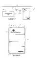
- FIG. 2is a front elevational view of the wireless communication device.
- FIG. 3is a front elevational view of the wireless communication device at an intermediate processing step.
- FIG. 4is cross-sectional view, taken along line 4 — 4 , of the wireless communication device shown in FIG. 3 at an intermediate processing step.
- FIG. 5is a cross-sectional view of the wireless communication device at a processing step subsequent to FIG. 4 .
- FIG. 6is a cross-sectional view of the wireless communication device at a processing step subsequent to FIG. 5 .
- FIG. 7is a cross-sectional view, similar to FIG. 4 , of an alternative intermediate processing step.
- FIG. 8is a cross-sectional view of a first embodiment of the wireless communication device.
- FIG. 9is a cross-sectional view of another embodiment of the wireless communication device.
- the wireless communication devicesare fabricated in card configurations (which include tags or stamps) according to first and second aspects of the present invention.
- the embodimentsare illustrative and other configurations of a wireless communication device according to the present invention are possible.
- Certain embodiments of the wireless communication device according to the inventioncomprise radio frequency identification devices (RFID) and remote intelligent communication devices (RIC).
- RFIDradio frequency identification devices
- RICremote intelligent communication devices
- a remote intelligent communication device or wireless communication device 10comprises part of a communication system 12 .
- the remote intelligent communication deviceis capable of functions other than the identifying function of a radio frequency identification device.
- a preferred embodiment of the remote intelligent communication deviceincludes a processor.
- the communication system 12 shown in FIG. 1further includes an interrogator unit 14 .
- An exemplary interrogator 14is described in detail in U.S. patent application Ser. No. 08/806,158, filed Feb. 25, 1997, assigned to the assignee of the present application and incorporated herein by reference.
- the wireless communication device 10communicates via wireless electronic signals, such as radio frequency (RF) signals, with the interrogator unit 14 . Radio frequency signals including microwave signals are utilized for communications in a preferred embodiment of communication system 12 .
- the communication system 12includes an antenna 16 coupled to the interrogator unit 14 .
- the wireless communication device 10includes an insulative substrate or layer of supportive material 18 .
- substraterefers to any supporting or supportive structure, including but not limited to, a supportive single layer of material or multiple layer constructions.
- Example materials for the substrate 18comprise polyester, polyethylene or polyimide film having a thickness of 4–6 mils (thousandths of an inch).
- Substrate 18provides a first or lower portion of a housing for the wireless communication device 10 and defines an outer periphery 21 of the device 10 .
- Substrate 18includes a plurality of peripheral edges 17 .
- ink layer 19is applied to substrate 18 in preferred embodiments of the invention.
- Ink layer 19enhances the appearance of the device 10 and conceals internal components and circuitry provided therein.
- a portion of ink layer 19has been peeled away in FIG. 3 to reveal a portion of an upper surface 25 of substrate 18 .
- plural ink layersare provided upon upper surface 25 .
- a support surface 20is provided to support components and circuitry formed in later processing steps upon substrate 18 .
- support surface 20comprises an upper surface thereof as shown in FIG. 3 .
- upper surface 25 of substrate 18operates as the support surface if ink is not applied to substrate 18 .
- a patterned conductive trace 30is formed or applied over the substrate 18 and atop the support surface 20 .
- Conductive trace 30is formed upon ink layer 19 , if present, or upon substrate 18 if no ink layer is provided.
- a preferred conductive trace 30comprises printed thick film (PTF).
- the printed thick filmcomprises silver and polyester dissolved into a solvent.
- One manner of forming or applying the conductive trace 30is to screen or stencil print the ink on the support surface 20 through conventional screen printing techniques.
- the printed thick filmis preferably heat cured to flash off the solvent and UV cured to react UV materials present in the printed thick film.
- the conductive trace 30forms desired electrical connections with and between electronic components which will be described below.
- substrate 18forms a portion of a larger roll of polyester film material used to manufacture multiple devices 10 .
- the printing of conductive trace 30can take place simultaneously for a number of the to-be-formed wireless communication devices.
- the illustrated conductive trace 30includes an electrical connection 28 , a first connection terminal 53 (shown in phantom in FIG. 3 ) and a second connection terminal 58 .
- Conductive trace 30additionally defines transmit and receive antennas 32 , 34 in one embodiment of the invention.
- Antennas 32 , 34are suitable for respectively transmitting and receiving wireless signals or RF energy.
- Transmit antenna 32constitutes a loop antenna having outer peripheral edges 37 .
- Receive antenna 34constitutes two elongated portions individually having horizontal peripheral edges 38 a , which extend in opposing directions, and substantially parallel vertical peripheral edges 38 b.
- Both transmit and receive operationsare implemented with a single antenna in alternative embodiments of the present invention.
- Both antennas 32 , 34preferably extend or lie within the confines of peripheral edges 17 and outer periphery 21 and define a plane (shown in FIG. 4 ).
- a wireless communication device 10includes a power source 52 , integrated circuit 54 , and capacitor 55 .
- Power source 52 , capacitor 55 , and integrated circuit 54are provided and mounted on support surface 20 and supported by substrate 18 .
- the depicted power source 52is disposed within transmit antenna 32 of wireless communication device 10 .
- Capacitor 55is electrically coupled with loop antenna 32 and integrated circuit 54 in the illustrated embodiment.
- Power source 52provides operational power to the wireless communication device 10 and selected components therein, including integrated circuit 54 .
- power source 52comprises a battery.
- power source 52is preferably a thin profile battery which includes first and second terminals of opposite polarity. More particularly, the battery has a lid or negative (i.e., ground) terminal or electrode, and a can or positive (i.e., power) terminal or electrode.
- Conductive epoxyis applied over desired areas of support surface 20 using conventional printing techniques, such as stencil or screen printing, to assist in component attachment described just below. Alternately, solder or another conductive material is employed instead of conductive epoxy.
- the power source 52is provided and mounted on support surface 20 using the conductive epoxy.
- Integrated circuit 54 and capacitor 55are also provided and mounted or conductively bonded on the support surface 20 using the conductive epoxy. Integrated circuit 54 can be mounted either before or after the power source 52 is mounted on the support surface 20 .
- Integrated circuit 54includes suitable circuitry for providing wireless communications.
- integrated circuit 54includes a processor 62 , memory 63 , and wireless communication circuitry or transponder circuitry 64 (components 62 , 63 , 64 are shown in phantom in FIG. 3 ) for providing wireless communications with interrogator unit 14 .
- An exemplary and preferred integrated circuit 54is described in U.S. patent application Ser. No. 08/705,043, incorporated by reference above.
- transponder circuitry 64includes a transmitter and a receiver respectively operable to transmit and receive wireless electronic signals.
- transponder circuitry 64is operable to transmit an identification signal responsive to receiving a polling signal from interrogator 14 .
- processor 62is configured to process the received polling signal to detect a predefined code within the polling signal. Responsive to the detection of an appropriate polling signal, processor 62 instructs transponder circuitry 64 to output an identification signal.
- the identification signalcontains an appropriate code to identify the particular device 10 transmitting the identification signal in certain embodiments.
- the identification and polling signalsare respectively transmitted and received via antennas 32 , 34 of the device 10 .
- First and second connection terminals 53 , 58are coupled to the integrated circuit 54 by conductive epoxy in accordance with a preferred embodiment of the invention.
- the conductive epoxyalso electrically connects the first terminal of the power source 52 to the first connection terminal 53 .
- power source 52is placed lid down such that the conductive epoxy makes electrical contact between the negative terminal of the power source 52 and the first connection terminal 53 .
- Power source 52has a perimetral edge 56 , defining the second power source terminal, which is provided adjacent second connection terminal 58 .
- perimetral edge 56 of the power source 52is cylindrical, and the connection terminal 58 is arcuate and has a radius slightly greater than the radius of the power source 52 , so that connection terminal 58 is closely spaced apart from the edge 56 of power source 52 .
- conductive epoxyis dispensed relative to perimetral edge 56 and electrically connects perimetral edge 56 with connection terminal 58 .
- perimetral edge 56defines the can of the power source 52 .
- the conductive epoxyconnects the positive terminal of the power source 52 to connection terminal 58 .
- the conductive epoxyis then cured.
- an electrical connectionsuch as a conductive post or pin 26
- a pick and place surface mount machine 70shown in FIG. 4
- the integrated circuit 54 and the capacitor 55are also placed using the surface mount machine 70 .
- Conductive pin 26is utilized to provide electrical conductivity between electrical connection 28 , conductive trace 30 , and other conductive layers (e.g., a ground plane layer described below) of the wireless communication device 10 .
- Other methods of forming connection 26may be utilized.
- an encapsulantsuch as encapsulating epoxy material, is subsequently formed following component attachment to provide a first encapsulant layer or insulative layer 60 .
- insulative layer 60is provided over the entire support surface 20 .
- Insulative layer 60encapsulates or envelopes the antennas 32 , 34 , integrated circuit 54 , power source 52 , conductive circuitry 30 , capacitor 55 , and at least a portion of the support surface 20 of substrate 18 .
- Insulative layer 60defines an intermediate portion of a housing for the wireless communication device 10 .
- Insulative layer 60operates to insulate the components (i.e., antennas 32 , 34 , integrated circuit 54 , power source 52 , conductive circuitry 30 and capacitor 55 ) from other conductive portions of the wireless communication device 10 formed in subsequent processing steps described below.
- An exemplary encapsulantis a flowable encapsulant.
- the flowable encapsulantis applied over substrate 18 and subsequently cured following the appropriate covering of the desired components.
- such encapsulantconstitutes a two-part epoxy including fillers, such as silicon and calcium carbonate.
- the preferred two-part epoxyis sufficient to provide a desired degree of flexible rigidity.
- encapsulant materials of insulative layer 60can be used in accordance with the present invention.
- the thickness of insulative layer 60can be varied. Using alternative encapsulant materials and the adjusting of the dimensions of insulative layer 60 alter the dielectric characteristics (i.e., dielectric constant) of layer 60 .
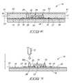
- wireless communication device 10is illustrated at an intermediate processing step.
- a portion of insulative layer 60is preferably removed.
- the removed portionis represented by the dimension “h” in FIG. 5 .
- Such removalprovides a substantially planar dielectric surface 65 of insulative layer 60 .
- Dielectric surface 65is substantially parallel to the plane 33 defined by antennas 32 , 34 .
- the portionis removed by sanding insulative layer 60 to provide planar surface 65 according to one processing method of the present invention.
- Insulative layer 60is preferably sanded to a predetermined thickness, such as 90 mils. In other embodiments, the entire insulative layer 60 is utilized and removal of the upper portion of layer 60 is not implemented.
- connections 26 , 26 aIn embodiments where one of connections 26 , 26 a is provided (alternate connection 26 a is shown in FIGS. 7 and 9 ), sanding or partially removing insulative layer 60 exposes a top portion of the connection 26 , 26 a permitting electrical coupling therewith adjacent dielectric surface 65 .
- the thickness of insulative layer 60defines the distance between a conductive layer 22 (described below) and antennas 32 , 34 , provided adjacent opposing sides of layer 60 .
- the thickness of insulative layer 60is chosen as a function of the dielectric constant of the encapsulant and the desired frequency for communication.
- Conductive layer 22is formed or applied over the dielectric surface 65 thereof.
- Conductive layer 22includes peripheral edges 61 .
- conductive layer 22covers or is provided over the entire insulative dielectric surface 65 .
- conductive layer 22is patterned to cover predefined portions of dielectric surface 65 .
- the layer 22is preferably formed at least over antennas 32 , 34 . More specifically, the respective peripheral edges 37 , 38 of antennas 32 , 34 are provided within the confines of the peripheral edges 61 of conductive layer 22 .
- Conductive layer 22 formed upon dielectric surface 65is preferably substantially planar. In addition, conductive layer 22 is substantially parallel to the plane 33 defined by antennas 32 , 34 , as well as dielectric surface 65 .
- conductive layer 22comprises a stencil printed polymer thick film (PTF).
- the polymer thick filmis typically 70–73% overfilled.
- conductive layer 22is a conductive epoxy comprising approximately 70% metal.
- conductive layer 22comprises copper or gold foil laminated upon the dielectric surface 65 of insulative layer 60 .
- metalsuch as gold is sputtered upon dielectric surface 65 of insulative layer 60 to form conductive layer 22 .
- Conductive layer 22can be configured to operate as a ground plane and interact with antennas 32 , 34 .
- conductive layer 22can be used to form a radio frequency (RF) shield.
- RFradio frequency
- Conductive layer 22interacts with antennas 32 , 34 to improve the RF operation of wireless communication device 10 .
- conductive layer 22operates to shield some wireless electronic signals from the receive antenna 34 and reflect other wireless electronic signals toward the antenna 34 .
- Conductive layer 22includes a first side, which faces away from antennas 32 , 34 (opposite surface 65 ) and a second side, which faces antennas 32 , 34 (adjacent surface 65 ).
- Electronic signals received on the first side of the conductive layer 22are shielded or blocked by layer 22 from reaching the antennas 32 , 34 .
- Electronic signals received on the second side of the conductive layer 22which pass by or around antennas 32 , 34 , are reflected by layer 22 .
- wireless signals transmitted by communications device 10 via antenna 32are reflected by conductive layer 22 .
- wireless signals transmitted from antenna 32 which strike the second side of conductive layer 22are reflected thereby.
- Such shielding and reflecting by conductive layer 22provides a highly directional wireless communication device 10 .
- the provision of conductive layer 22 within wireless communication device 10results in robust wireless communications with interrogator 14 and provides increased reliability.
- the conductive layer 22is electrically connected with power source 52 in the illustrated embodiments of the present invention.
- Conductive layer 22can be electrically coupled with either the positive or negative terminal of power source 52 . Coupling of conductive layer 22 with one of the terminals of power source 52 provides layer 22 at the voltage potential of the respective terminal.
- conductive layer 22is electrically coupled with the ground (i.e., negative) terminal of power source 52 through the integrated circuit 54 .
- integrated circuit 54includes a first pin 35 internally connected with the ground terminal of power source 52 (not shown).
- First pin 35is additionally conductively bonded with electrical connection 28 of conductive trace 30 .
- Electrical connection 28is conductively coupled with connection pin 26 .
- Pin 26is connected with conductive layer 22 and provides electrical coupling of conductive layer 22 and power source 52 through insulative layer 60 .
- Coupling of one of the power terminals of power source 52 and ground plane/conductive layer 22provides layer 22 at a common reference voltage.
- electrically connecting ground plane/conductive layer 22 and the ground terminal of power source 52 via electrical connections 26 , 28electrically grounds layer 22 .
- ground plane/conductive layer 22is coupled with the power electrode of power source 52 via electrical connections 26 , 28 in other embodiments of the invention. Coupling ground plane/conductive layer 22 with the power electrode of power source 52 provides layer 22 at the positive potential of power source 52 .
- Pin 26is coupled directly with one of the terminals of power source 52 in other embodiments of the invention (not shown), thereby bypassing integrated circuit 54 .
- no electrical connectionis made to ground plane/conductive layer 22 .
- ground plane/conductive layer 22is insulated and the voltage of layer 22 is permitted to float.
- Electrical connection 26 aalso provides conductivity through insulative layer 60 .
- Connection 26 aelectrically couples conductive layer 22 and electrical connection 28 .
- electrical connection 26 acomprises conductive epoxy.
- a dispenser 72is utilized to dispense the conductive epoxy onto connection 28 of conductive trace 30 in the depicted embodiment.
- Connections 26 , 26 amay be formed at positions other than those illustrated in the depicted embodiments of device 10 .
- connections 26 , 26 amay be provided at any appropriate location to provide electrical coupling of a terminal of power source 52 and conductive layer 22 .
- an upper housing portion 66is preferably formed over the conductive layer 22 of the respective illustrated devices 10 .
- upper housing portion 66comprises a second encapsulant layer which covers and/or encapsulates the conductive layer 22 of the respective devices 10 .
- first and second encapsulant layers 60 , 66envelope the entire conductive layer 22 . Such is desired to insulate the conductive layer 22 .
- Second encapsulant layer 66may comprise the two-part encapsulant utilized to form insulative first encapsulant layer 60 . Following the provision of second encapsulant layer 66 upon conductive layer 22 , the encapsulant is subsequently cured forming a substantially void-free housing 27 or solid mass with substrate 18 and first encapsulant layer 60 .
- housing 27 of wireless communication device 10has a width of about 3.375 inches, a height of about 2.125 inches, and a thickness less than or equal to about 0.0625 inches.
Landscapes
- Engineering & Computer Science (AREA)
- Computer Hardware Design (AREA)
- Microelectronics & Electronic Packaging (AREA)
- Physics & Mathematics (AREA)
- General Physics & Mathematics (AREA)
- Theoretical Computer Science (AREA)
- Condensed Matter Physics & Semiconductors (AREA)
- Power Engineering (AREA)
- Details Of Aerials (AREA)
- Support Of Aerials (AREA)
Abstract
Description
Claims (97)
Priority Applications (2)
| Application Number | Priority Date | Filing Date | Title |
|---|---|---|---|
| US09/570,365US6980085B1 (en) | 1997-08-18 | 2000-04-13 | Wireless communication devices and methods of forming and operating the same |
| US11/312,669US20060097849A1 (en) | 1997-08-18 | 2005-12-19 | Wireless communication devices and methods of forming and operating the same |
Applications Claiming Priority (2)
| Application Number | Priority Date | Filing Date | Title |
|---|---|---|---|
| US91430597A | 1997-08-18 | 1997-08-18 | |
| US09/570,365US6980085B1 (en) | 1997-08-18 | 2000-04-13 | Wireless communication devices and methods of forming and operating the same |
Related Parent Applications (1)
| Application Number | Title | Priority Date | Filing Date |
|---|---|---|---|
| US91430597AContinuation | 1997-08-18 | 1997-08-18 |
Related Child Applications (1)
| Application Number | Title | Priority Date | Filing Date |
|---|---|---|---|
| US11/312,669ContinuationUS20060097849A1 (en) | 1997-08-18 | 2005-12-19 | Wireless communication devices and methods of forming and operating the same |
Publications (1)
| Publication Number | Publication Date |
|---|---|
| US6980085B1true US6980085B1 (en) | 2005-12-27 |
Family
ID=35482594
Family Applications (2)
| Application Number | Title | Priority Date | Filing Date |
|---|---|---|---|
| US09/570,365Expired - Fee RelatedUS6980085B1 (en) | 1997-08-18 | 2000-04-13 | Wireless communication devices and methods of forming and operating the same |
| US11/312,669AbandonedUS20060097849A1 (en) | 1997-08-18 | 2005-12-19 | Wireless communication devices and methods of forming and operating the same |
Family Applications After (1)
| Application Number | Title | Priority Date | Filing Date |
|---|---|---|---|
| US11/312,669AbandonedUS20060097849A1 (en) | 1997-08-18 | 2005-12-19 | Wireless communication devices and methods of forming and operating the same |
Country Status (1)
| Country | Link |
|---|---|
| US (2) | US6980085B1 (en) |
Cited By (4)
| Publication number | Priority date | Publication date | Assignee | Title |
|---|---|---|---|---|
| US7106201B2 (en) | 1997-08-20 | 2006-09-12 | Micron Technology, Inc. | Communication devices, remote intelligent communication devices, electronic communication devices, methods of forming remote intelligent communication devices and methods of forming a radio frequency identification device |
| US20070024447A1 (en)* | 2005-07-29 | 2007-02-01 | Burnside Walter D | Radio energy propagation channel network for detecting RFID tagged items |
| US7583192B2 (en) | 1992-08-12 | 2009-09-01 | Keystone Technology Solutions, Llc | Radio frequency identification device and method |
| US20180242455A1 (en)* | 2008-04-23 | 2018-08-23 | Skyworks Solutions, Inc. | 3-d stacking of active devices over passive devices |
Families Citing this family (4)
| Publication number | Priority date | Publication date | Assignee | Title |
|---|---|---|---|---|
| US20070131781A1 (en)* | 2005-12-08 | 2007-06-14 | Ncr Corporation | Radio frequency device |
| WO2008144331A1 (en)* | 2007-05-16 | 2008-11-27 | Mpt, Inc. | In-mold labeling system for containers |
| US7948384B1 (en)* | 2007-08-14 | 2011-05-24 | Mpt, Inc. | Placard having embedded RFID device for tracking objects |
| US12265868B2 (en)* | 2020-05-28 | 2025-04-01 | Linxens Holding | Document with shielding |
Citations (39)
| Publication number | Priority date | Publication date | Assignee | Title |
|---|---|---|---|---|
| US4075632A (en) | 1974-08-27 | 1978-02-21 | The United States Of America As Represented By The United States Department Of Energy | Interrogation, and detection system |
| US4631546A (en) | 1983-04-11 | 1986-12-23 | Rockwell International Corporation | Electronically rotated antenna apparatus |
| US4709201A (en) | 1985-10-24 | 1987-11-24 | General Electric Company | Portable radio battery pack with on-off switch |
| US4853705A (en) | 1988-05-11 | 1989-08-01 | Amtech Technology Corporation | Beam powered antenna |
| US4857893A (en) | 1986-07-18 | 1989-08-15 | Bi Inc. | Single chip transponder device |
| US4926182A (en) | 1986-05-30 | 1990-05-15 | Sharp Kabushiki Kaisha | Microwave data transmission apparatus |
| US5030940A (en) | 1990-08-02 | 1991-07-09 | Sensormatic Electronics Corporation | Electronic article surveillance tag and method for implementing same |
| US5061943A (en) | 1988-08-03 | 1991-10-29 | Agence Spatiale Europenne | Planar array antenna, comprising coplanar waveguide printed feed lines cooperating with apertures in a ground plane |
| US5138651A (en) | 1989-02-23 | 1992-08-11 | Fujitsu Limited | Cordless loud speaking telephone |
| US5151946A (en) | 1989-08-24 | 1992-09-29 | Technophone Limited | Variable configuration portable telephone |
| US5170173A (en) | 1992-04-27 | 1992-12-08 | Motorola, Inc. | Antenna coupling apparatus for cordless telephone |
| US5392049A (en) | 1990-07-24 | 1995-02-21 | Gunnarsson; Staffan | Device for positioning a first object relative to a second object |
| US5400039A (en) | 1991-12-27 | 1995-03-21 | Hitachi, Ltd. | Integrated multilayered microwave circuit |
| US5410749A (en) | 1992-12-09 | 1995-04-25 | Motorola, Inc. | Radio communication device having a microstrip antenna with integral receiver systems |
| US5442367A (en) | 1992-09-03 | 1995-08-15 | Sumitomo Metal Mining Co., Ltd. | Printed antenna with strip and slot radiators |
| US5448110A (en) | 1992-06-17 | 1995-09-05 | Micron Communications, Inc. | Enclosed transceiver |
| US5480842A (en)* | 1994-04-11 | 1996-01-02 | At&T Corp. | Method for fabricating thin, strong, and flexible die for smart cards |
| US5497168A (en) | 1992-05-01 | 1996-03-05 | Hughes Aircraft Company | Radiator bandwidth enhancement using dielectrics with inverse frequency dependence |
| US5528222A (en)* | 1994-09-09 | 1996-06-18 | International Business Machines Corporation | Radio frequency circuit and memory in thin flexible package |
| US5550547A (en)* | 1994-09-12 | 1996-08-27 | International Business Machines Corporation | Multiple item radio frequency tag identification protocol |
| US5552790A (en) | 1992-01-23 | 1996-09-03 | Saab-Scania Combitech Aktiebolag | Device for wireless transfer of information |
| US5569879A (en) | 1991-02-19 | 1996-10-29 | Gemplus Card International | Integrated circuit micromodule obtained by the continuous assembly of patterned strips |
| US5621412A (en) | 1994-04-26 | 1997-04-15 | Texas Instruments Incorporated | Multi-stage transponder wake-up, method and structure |
| US5642103A (en) | 1990-10-01 | 1997-06-24 | Sharp Kabushiki Kaisha | Transponder used in a remote identification system |
| US5649295A (en) | 1995-06-19 | 1997-07-15 | Lucent Technologies Inc. | Dual mode modulated backscatter system |
| US5649296A (en) | 1995-06-19 | 1997-07-15 | Lucent Technologies Inc. | Full duplex modulated backscatter system |
| US5682143A (en)* | 1994-09-09 | 1997-10-28 | International Business Machines Corporation | Radio frequency identification tag |
| US5708419A (en) | 1996-07-22 | 1998-01-13 | Checkpoint Systems, Inc. | Method of wire bonding an integrated circuit to an ultraflexible substrate |
| US5793305A (en) | 1991-04-03 | 1998-08-11 | Turner; Leigh Holbrook | Article sorting system |
| US5815120A (en) | 1996-02-28 | 1998-09-29 | International Business Machines Corporation | Radio frequency local area network adapter card structure and method of manufacture |
| US5859587A (en) | 1996-09-26 | 1999-01-12 | Sensormatic Electronics Corporation | Data communication and electronic article surveillance tag |
| US5939984A (en) | 1997-12-31 | 1999-08-17 | Intermec Ip Corp. | Combination radio frequency transponder (RF Tag) and magnetic electronic article surveillance (EAS) material |
| US5970393A (en)* | 1997-02-25 | 1999-10-19 | Polytechnic University | Integrated micro-strip antenna apparatus and a system utilizing the same for wireless communications for sensing and actuation purposes |
| US5995048A (en)* | 1996-05-31 | 1999-11-30 | Lucent Technologies Inc. | Quarter wave patch antenna |
| US6049278A (en) | 1997-03-24 | 2000-04-11 | Northrop Grumman Corporation | Monitor tag with patch antenna |
| US6118379A (en) | 1997-12-31 | 2000-09-12 | Intermec Ip Corp. | Radio frequency identification transponder having a spiral antenna |
| US6133836A (en) | 1998-02-27 | 2000-10-17 | Micron Technology, Inc. | Wireless communication and identification packages, communication systems, methods of communicating, and methods of forming a communication device |
| US6339385B1 (en)* | 1997-08-20 | 2002-01-15 | Micron Technology, Inc. | Electronic communication devices, methods of forming electrical communication devices, and communication methods |
| US6359588B1 (en) | 1997-07-11 | 2002-03-19 | Nortel Networks Limited | Patch antenna |
Family Cites Families (57)
| Publication number | Priority date | Publication date | Assignee | Title |
|---|---|---|---|---|
| US526328A (en)* | 1894-09-18 | Switch apparatus | ||
| US3573705A (en)* | 1969-03-21 | 1971-04-06 | Dominion Auto Access | Bulb-mounting assembly |
| US3660916A (en)* | 1969-11-10 | 1972-05-09 | Bio Logics Inc | Identification system |
| US3702464A (en)* | 1971-05-04 | 1972-11-07 | Ibm | Information card |
| US3947930A (en)* | 1974-10-30 | 1976-04-06 | I. D. Engineering, Inc. | Anti-theft fastening device and tool for releasing same |
| US4065343A (en)* | 1975-11-14 | 1977-12-27 | Rexnord Inc. | Label system for package and baggage handling |
| US4188629A (en)* | 1976-07-19 | 1980-02-12 | Motorola, Inc. | Passive navigation system with frequency coding |
| GB1529541A (en)* | 1977-02-11 | 1978-10-25 | Philips Electronic Associated | Microwave antenna |
| CA1119702A (en)* | 1978-03-30 | 1982-03-09 | Her Majesty The Queen In Right Of Canada As Represented By The Minister Of National Defence Of Her Majesty's Canadian Government | Parametric frequency division |
| US4170773A (en)* | 1978-05-05 | 1979-10-09 | The Boeing Company | Precision approach sensor system for aircraft |
| US4242663A (en)* | 1979-02-01 | 1980-12-30 | Lockheed Electronics Corporation | Electronic identification system |
| US4587038A (en)* | 1980-06-26 | 1986-05-06 | Canon Kabushiki Kaisha | Electro-optic display device and a method of producing the same |
| US4471344A (en)* | 1980-10-09 | 1984-09-11 | Ici Americas Inc. | Dual frequency anti-theft system |
| US4490721A (en)* | 1980-11-17 | 1984-12-25 | Ball Corporation | Monolithic microwave integrated circuit with integral array antenna |
| US4509053A (en)* | 1982-07-26 | 1985-04-02 | Sensor Systems, Inc. | Blade antenna with shaped dielectric |
| US4623893A (en)* | 1983-12-06 | 1986-11-18 | State Of Israel, Ministry Of Defense, Rafael Armament & Development Authority | Microstrip antenna and antenna array |
| US4656478A (en)* | 1984-07-30 | 1987-04-07 | Asulab S.A. | Passive transponder for locating avalanche victims |
| US4603326A (en)* | 1984-09-14 | 1986-07-29 | Ici Americas Inc. | Anti-theft detector responsive to a chemical agent |
| US4634849A (en)* | 1985-04-02 | 1987-01-06 | Klingen Leonard G | Uniquely numbered baggage split tag and system for handling baggage |
| US5020136A (en)* | 1986-04-21 | 1991-05-28 | Motorola, Inc. | Battery pack antenna suitable for use with two-way portable transceivers |
| US4751513A (en)* | 1986-05-02 | 1988-06-14 | Rca Corporation | Light controlled antennas |
| US4814943A (en)* | 1986-06-04 | 1989-03-21 | Oki Electric Industry Co., Ltd. | Printed circuit devices using thermoplastic resin cover plate |
| US4737789A (en)* | 1986-12-02 | 1988-04-12 | X Cyte, Inc. | Inductive antenna coupling for a surface acoustic wave transponder |
| US4855583A (en)* | 1987-08-17 | 1989-08-08 | Figgie International, Inc. | Structure and method of making combination proximity/insertion identification cards |
| US4830038A (en)* | 1988-01-20 | 1989-05-16 | Atlantic Richfield Company | Photovoltaic module |
| JPH01245721A (en)* | 1988-03-28 | 1989-09-29 | Matsushita Electric Works Ltd | Radio equipment |
| US4884208A (en)* | 1988-05-16 | 1989-11-28 | Equipment Tracking Network, Inc. | System for continuously establishing and indicating the location of a movable object |
| US4866453A (en)* | 1988-08-15 | 1989-09-12 | General Motors Corporation | Vehicle slot antenna with parasitic slot |
| JPH03263903A (en)* | 1989-04-28 | 1991-11-25 | Misao Haishi | Miniature antenna |
| US5192947A (en)* | 1990-02-02 | 1993-03-09 | Simon Neustein | Credit card pager apparatus |
| US5055659A (en)* | 1990-02-06 | 1991-10-08 | Amtech Technology Corp. | High speed system for reading and writing data from and into remote tags |
| US5376943A (en)* | 1990-09-07 | 1994-12-27 | Plessey Semiconductors Limited | Moving vehicle transponder |
| US5115223A (en)* | 1990-09-20 | 1992-05-19 | Moody Thomas O | Personnel location monitoring system and method |
| JP3100716B2 (en)* | 1991-01-04 | 2000-10-23 | シーエスアイアール | Identification device |
| FR2674052A1 (en)* | 1991-03-15 | 1992-09-18 | Philips Composants | MICROCIRCUIT CARD. |
| US5250843A (en)* | 1991-03-27 | 1993-10-05 | Integrated System Assemblies Corp. | Multichip integrated circuit modules |
| US5231273A (en)* | 1991-04-09 | 1993-07-27 | Comtec Industries | Inventory management system |
| JP2993186B2 (en)* | 1991-06-28 | 1999-12-20 | 株式会社デンソー | Aircraft baggage management system |
| US5112253A (en)* | 1991-08-15 | 1992-05-12 | Amphenol Corporation | Arrangement for removably mounting a transient suppression or electrical filter device in an electrical connector |
| JPH05169885A (en)* | 1991-12-26 | 1993-07-09 | Mitsubishi Electric Corp | Thin IC card |
| US5414221A (en)* | 1991-12-31 | 1995-05-09 | Intel Corporation | Embedded ground plane and shielding structures using sidewall insulators in high frequency circuits having vias |
| US5144261A (en)* | 1992-01-15 | 1992-09-01 | The United States Of America As Represented By The Secretary Of The Army | Optically injection locked resonant tunnel diode oscillator |
| US5252783A (en)* | 1992-02-10 | 1993-10-12 | Motorola, Inc. | Semiconductor package |
| US7158031B2 (en)* | 1992-08-12 | 2007-01-02 | Micron Technology, Inc. | Thin, flexible, RFID label and system for use |
| US5491482A (en)* | 1992-12-29 | 1996-02-13 | David Sarnoff Research Center, Inc. | Electronic system and method for remote identification of coded articles and the like |
| US5480834A (en)* | 1993-12-13 | 1996-01-02 | Micron Communications, Inc. | Process of manufacturing an electrical bonding interconnect having a metal bond pad portion and having a conductive epoxy portion comprising an oxide reducing agent |
| DE19527359A1 (en)* | 1995-07-26 | 1997-02-13 | Giesecke & Devrient Gmbh | Circuit unit and method for manufacturing a circuit unit |
| US5817207A (en)* | 1995-10-17 | 1998-10-06 | Leighton; Keith R. | Radio frequency identification card and hot lamination process for the manufacture of radio frequency identification cards |
| US6130602A (en)* | 1996-05-13 | 2000-10-10 | Micron Technology, Inc. | Radio frequency data communications device |
| US5963132A (en)* | 1996-10-11 | 1999-10-05 | Avid Indentification Systems, Inc. | Encapsulated implantable transponder |
| US5945938A (en)* | 1996-11-14 | 1999-08-31 | National University Of Singapore | RF identification transponder |
| US5988510A (en)* | 1997-02-13 | 1999-11-23 | Micron Communications, Inc. | Tamper resistant smart card and method of protecting data in a smart card |
| US6052062A (en)* | 1997-08-20 | 2000-04-18 | Micron Technology, Inc. | Cards, communication devices, and methods of forming and encoding visibly perceptible information on the same |
| US6043745A (en)* | 1997-11-13 | 2000-03-28 | Micron Technology, Inc. | Electronic devices and methods of forming electronic devices |
| US6030423A (en)* | 1998-02-12 | 2000-02-29 | Micron Technology, Inc. | Thin profile battery bonding method and method of conductively interconnecting electronic components |
| US6714121B1 (en)* | 1999-08-09 | 2004-03-30 | Micron Technology, Inc. | RFID material tracking method and apparatus |
| JP5395429B2 (en)* | 2005-06-03 | 2014-01-22 | シナプティクス インコーポレイテッド | Method and system for detecting capacitance using sigma delta measurement |
- 2000
- 2000-04-13USUS09/570,365patent/US6980085B1/ennot_activeExpired - Fee Related
- 2005
- 2005-12-19USUS11/312,669patent/US20060097849A1/ennot_activeAbandoned
Patent Citations (39)
| Publication number | Priority date | Publication date | Assignee | Title |
|---|---|---|---|---|
| US4075632A (en) | 1974-08-27 | 1978-02-21 | The United States Of America As Represented By The United States Department Of Energy | Interrogation, and detection system |
| US4631546A (en) | 1983-04-11 | 1986-12-23 | Rockwell International Corporation | Electronically rotated antenna apparatus |
| US4709201A (en) | 1985-10-24 | 1987-11-24 | General Electric Company | Portable radio battery pack with on-off switch |
| US4926182A (en) | 1986-05-30 | 1990-05-15 | Sharp Kabushiki Kaisha | Microwave data transmission apparatus |
| US4857893A (en) | 1986-07-18 | 1989-08-15 | Bi Inc. | Single chip transponder device |
| US4853705A (en) | 1988-05-11 | 1989-08-01 | Amtech Technology Corporation | Beam powered antenna |
| US5061943A (en) | 1988-08-03 | 1991-10-29 | Agence Spatiale Europenne | Planar array antenna, comprising coplanar waveguide printed feed lines cooperating with apertures in a ground plane |
| US5138651A (en) | 1989-02-23 | 1992-08-11 | Fujitsu Limited | Cordless loud speaking telephone |
| US5151946A (en) | 1989-08-24 | 1992-09-29 | Technophone Limited | Variable configuration portable telephone |
| US5392049A (en) | 1990-07-24 | 1995-02-21 | Gunnarsson; Staffan | Device for positioning a first object relative to a second object |
| US5030940A (en) | 1990-08-02 | 1991-07-09 | Sensormatic Electronics Corporation | Electronic article surveillance tag and method for implementing same |
| US5642103A (en) | 1990-10-01 | 1997-06-24 | Sharp Kabushiki Kaisha | Transponder used in a remote identification system |
| US5569879A (en) | 1991-02-19 | 1996-10-29 | Gemplus Card International | Integrated circuit micromodule obtained by the continuous assembly of patterned strips |
| US5793305A (en) | 1991-04-03 | 1998-08-11 | Turner; Leigh Holbrook | Article sorting system |
| US5400039A (en) | 1991-12-27 | 1995-03-21 | Hitachi, Ltd. | Integrated multilayered microwave circuit |
| US5552790A (en) | 1992-01-23 | 1996-09-03 | Saab-Scania Combitech Aktiebolag | Device for wireless transfer of information |
| US5170173A (en) | 1992-04-27 | 1992-12-08 | Motorola, Inc. | Antenna coupling apparatus for cordless telephone |
| US5497168A (en) | 1992-05-01 | 1996-03-05 | Hughes Aircraft Company | Radiator bandwidth enhancement using dielectrics with inverse frequency dependence |
| US5448110A (en) | 1992-06-17 | 1995-09-05 | Micron Communications, Inc. | Enclosed transceiver |
| US5442367A (en) | 1992-09-03 | 1995-08-15 | Sumitomo Metal Mining Co., Ltd. | Printed antenna with strip and slot radiators |
| US5410749A (en) | 1992-12-09 | 1995-04-25 | Motorola, Inc. | Radio communication device having a microstrip antenna with integral receiver systems |
| US5480842A (en)* | 1994-04-11 | 1996-01-02 | At&T Corp. | Method for fabricating thin, strong, and flexible die for smart cards |
| US5621412A (en) | 1994-04-26 | 1997-04-15 | Texas Instruments Incorporated | Multi-stage transponder wake-up, method and structure |
| US5528222A (en)* | 1994-09-09 | 1996-06-18 | International Business Machines Corporation | Radio frequency circuit and memory in thin flexible package |
| US5682143A (en)* | 1994-09-09 | 1997-10-28 | International Business Machines Corporation | Radio frequency identification tag |
| US5550547A (en)* | 1994-09-12 | 1996-08-27 | International Business Machines Corporation | Multiple item radio frequency tag identification protocol |
| US5649296A (en) | 1995-06-19 | 1997-07-15 | Lucent Technologies Inc. | Full duplex modulated backscatter system |
| US5649295A (en) | 1995-06-19 | 1997-07-15 | Lucent Technologies Inc. | Dual mode modulated backscatter system |
| US5815120A (en) | 1996-02-28 | 1998-09-29 | International Business Machines Corporation | Radio frequency local area network adapter card structure and method of manufacture |
| US5995048A (en)* | 1996-05-31 | 1999-11-30 | Lucent Technologies Inc. | Quarter wave patch antenna |
| US5708419A (en) | 1996-07-22 | 1998-01-13 | Checkpoint Systems, Inc. | Method of wire bonding an integrated circuit to an ultraflexible substrate |
| US5859587A (en) | 1996-09-26 | 1999-01-12 | Sensormatic Electronics Corporation | Data communication and electronic article surveillance tag |
| US5970393A (en)* | 1997-02-25 | 1999-10-19 | Polytechnic University | Integrated micro-strip antenna apparatus and a system utilizing the same for wireless communications for sensing and actuation purposes |
| US6049278A (en) | 1997-03-24 | 2000-04-11 | Northrop Grumman Corporation | Monitor tag with patch antenna |
| US6359588B1 (en) | 1997-07-11 | 2002-03-19 | Nortel Networks Limited | Patch antenna |
| US6339385B1 (en)* | 1997-08-20 | 2002-01-15 | Micron Technology, Inc. | Electronic communication devices, methods of forming electrical communication devices, and communication methods |
| US5939984A (en) | 1997-12-31 | 1999-08-17 | Intermec Ip Corp. | Combination radio frequency transponder (RF Tag) and magnetic electronic article surveillance (EAS) material |
| US6118379A (en) | 1997-12-31 | 2000-09-12 | Intermec Ip Corp. | Radio frequency identification transponder having a spiral antenna |
| US6133836A (en) | 1998-02-27 | 2000-10-17 | Micron Technology, Inc. | Wireless communication and identification packages, communication systems, methods of communicating, and methods of forming a communication device |
Non-Patent Citations (3)
| Title |
|---|
| Kraus, John D., ANTENNAS Second Edition, McGraw-Hill, Inc., New York, 1988, pp. 460-477, 716-725. |
| U.S. Appl. No. 08/926,595, Mark E. Tuttle; Original Application filed Aug. 20, 1997;Amendent filed Feb. 22, 2000; Amendment filed Sep. 19, 2000; CPA filed Apr. 13, 2000; CPA filed Nov. 15, 1999; Amendment filed Apr. 21, 1999l Pending Claims. |
| U.S. Appl. No. 09/660,537, Freddie w. Smith, Preliminary Amendment; filed Sep. 13, 2000; Parent Application as filed with Preliminary Amendment; Pending Claims. |
Cited By (10)
| Publication number | Priority date | Publication date | Assignee | Title |
|---|---|---|---|---|
| US7583192B2 (en) | 1992-08-12 | 2009-09-01 | Keystone Technology Solutions, Llc | Radio frequency identification device and method |
| US7746230B2 (en) | 1992-08-12 | 2010-06-29 | Round Rock Research, Llc | Radio frequency identification device and method |
| US8018340B2 (en) | 1992-08-12 | 2011-09-13 | Round Rock Research, Llc | System and method to track articles at a point of origin and at a point of destination using RFID |
| US7106201B2 (en) | 1997-08-20 | 2006-09-12 | Micron Technology, Inc. | Communication devices, remote intelligent communication devices, electronic communication devices, methods of forming remote intelligent communication devices and methods of forming a radio frequency identification device |
| US20070007345A1 (en)* | 1997-08-20 | 2007-01-11 | Tuttle Mark E | Electronic communication devices, methods of forming electrical communication devices, and communications methods |
| US20070290862A1 (en)* | 1997-08-20 | 2007-12-20 | Tuttle Mark E | Electronic Communication Devices, Methods Of Forming Electrical Communication Devices, And Communications Methods |
| US7839285B2 (en)* | 1997-08-20 | 2010-11-23 | Round Rock Resarch, LLC | Electronic communication devices, methods of forming electrical communication devices, and communications methods |
| US7948382B2 (en) | 1997-08-20 | 2011-05-24 | Round Rock Research, Llc | Electronic communication devices, methods of forming electrical communication devices, and communications methods |
| US20070024447A1 (en)* | 2005-07-29 | 2007-02-01 | Burnside Walter D | Radio energy propagation channel network for detecting RFID tagged items |
| US20180242455A1 (en)* | 2008-04-23 | 2018-08-23 | Skyworks Solutions, Inc. | 3-d stacking of active devices over passive devices |
Also Published As
| Publication number | Publication date |
|---|---|
| US20060097849A1 (en) | 2006-05-11 |
Similar Documents
| Publication | Publication Date | Title |
|---|---|---|
| US7839285B2 (en) | Electronic communication devices, methods of forming electrical communication devices, and communications methods | |
| US6133836A (en) | Wireless communication and identification packages, communication systems, methods of communicating, and methods of forming a communication device | |
| US6031459A (en) | Wireless communication devices, radio frequency identification devices, and methods of forming wireless communication devices and radio frequency identification devices | |
| US6585165B1 (en) | IC card having a mica capacitor | |
| US7221257B1 (en) | Wireless communication devices, radio frequency identification devices, methods of forming a wireless communication device, and methods of forming a radio frequency identification device | |
| US5055968A (en) | Thin electronic device having an integrated circuit chip and a power battery and a method for producing same | |
| US6177859B1 (en) | Radio frequency communication apparatus and methods of forming a radio frequency communication apparatus | |
| US6043745A (en) | Electronic devices and methods of forming electronic devices | |
| US8025237B2 (en) | Antenna built-in module, card type information device, and methods for manufacturing them | |
| US6094138A (en) | Integrated circuit assembly and method of assembly | |
| US6900536B1 (en) | Method for producing an electrical circuit | |
| AU2003243162A2 (en) | Method for producing an electrical circuit | |
| US6666379B2 (en) | Method of fabricating a wireless radio frequency identification device | |
| US6980085B1 (en) | Wireless communication devices and methods of forming and operating the same | |
| US20210406636A1 (en) | Electronic module for chip card | |
| US6285561B1 (en) | Data carrier module device having integrated circuit and transmission coil connection contacts covered by a common protective cap | |
| JPH1111058A (en) | Ic module and ic card employing this | |
| JPH11184995A (en) | Antenna device and non-contact ic card using the same | |
| JPH0457401A (en) | High frequency antenna for traveling object identification device | |
| JPH0530306B2 (en) |
Legal Events
| Date | Code | Title | Description |
|---|---|---|---|
| FEPP | Fee payment procedure | Free format text:PAYOR NUMBER ASSIGNED (ORIGINAL EVENT CODE: ASPN); ENTITY STATUS OF PATENT OWNER: LARGE ENTITY | |
| AS | Assignment | Owner name:KEYSTONE TECHNOLOGY SOLUTIONS, LLC, IDAHO Free format text:ASSIGNMENT OF ASSIGNORS INTEREST;ASSIGNOR:MICRON TECHNOLOGY, INC.;REEL/FRAME:019825/0542 Effective date:20070628 Owner name:KEYSTONE TECHNOLOGY SOLUTIONS, LLC,IDAHO Free format text:ASSIGNMENT OF ASSIGNORS INTEREST;ASSIGNOR:MICRON TECHNOLOGY, INC.;REEL/FRAME:019825/0542 Effective date:20070628 | |
| FPAY | Fee payment | Year of fee payment:4 | |
| AS | Assignment | Owner name:ROUND ROCK RESEARCH, LLC,NEW YORK Free format text:ASSIGNMENT OF ASSIGNORS INTEREST;ASSIGNOR:MICRON TECHNOLOGY, INC.;REEL/FRAME:023786/0416 Effective date:20091223 Owner name:ROUND ROCK RESEARCH, LLC, NEW YORK Free format text:ASSIGNMENT OF ASSIGNORS INTEREST;ASSIGNOR:MICRON TECHNOLOGY, INC.;REEL/FRAME:023786/0416 Effective date:20091223 | |
| AS | Assignment | Owner name:MICRON TECHNOLOGY, INC., IDAHO Free format text:ASSIGNMENT OF ASSIGNORS INTEREST;ASSIGNOR:KEYSTONE TECHNOLOGY SOLUTIONS, LLC;REEL/FRAME:023839/0881 Effective date:20091222 Owner name:MICRON TECHNOLOGY, INC.,IDAHO Free format text:ASSIGNMENT OF ASSIGNORS INTEREST;ASSIGNOR:KEYSTONE TECHNOLOGY SOLUTIONS, LLC;REEL/FRAME:023839/0881 Effective date:20091222 | |
| FPAY | Fee payment | Year of fee payment:8 | |
| REMI | Maintenance fee reminder mailed | ||
| LAPS | Lapse for failure to pay maintenance fees | Free format text:PATENT EXPIRED FOR FAILURE TO PAY MAINTENANCE FEES (ORIGINAL EVENT CODE: EXP.) | |
| STCH | Information on status: patent discontinuation | Free format text:PATENT EXPIRED DUE TO NONPAYMENT OF MAINTENANCE FEES UNDER 37 CFR 1.362 | |
| FP | Lapsed due to failure to pay maintenance fee | Effective date:20171227 |