US6979872B2 - Modules integrating MEMS devices with pre-processed electronic circuitry, and methods for fabricating such modules - Google Patents
Modules integrating MEMS devices with pre-processed electronic circuitry, and methods for fabricating such modulesDownload PDFInfo
- Publication number
- US6979872B2 US6979872B2US10/438,512US43851203AUS6979872B2US 6979872 B2US6979872 B2US 6979872B2US 43851203 AUS43851203 AUS 43851203AUS 6979872 B2US6979872 B2US 6979872B2
- Authority
- US
- United States
- Prior art keywords
- module
- mems device
- electronic circuitry
- mems
- substrate
- Prior art date
- Legal status (The legal status is an assumption and is not a legal conclusion. Google has not performed a legal analysis and makes no representation as to the accuracy of the status listed.)
- Expired - Lifetime, expires
Links
- 238000000034methodMethods0.000titleabstractdescription22
- 239000000758substrateSubstances0.000claimsabstractdescription32
- 239000000853adhesiveSubstances0.000claimsdescription21
- 230000001070adhesive effectEffects0.000claimsdescription21
- 239000004020conductorSubstances0.000claimsdescription6
- 239000004593EpoxySubstances0.000claimsdescription3
- UMIVXZPTRXBADB-UHFFFAOYSA-NbenzocyclobuteneChemical compoundC1=CC=C2CCC2=C1UMIVXZPTRXBADB-UHFFFAOYSA-N0.000claimsdescription3
- 239000003990capacitorSubstances0.000claimsdescription3
- 239000004642PolyimideSubstances0.000claimsdescription2
- 238000005304joiningMethods0.000claimsdescription2
- 229920002480polybenzimidazolePolymers0.000claimsdescription2
- 229920001721polyimidePolymers0.000claimsdescription2
- 229920001296polysiloxanePolymers0.000claimsdescription2
- 229920002635polyurethanePolymers0.000claimsdescription2
- 239000004814polyurethaneSubstances0.000claimsdescription2
- 239000004693PolybenzimidazoleSubstances0.000claims1
- NIXOWILDQLNWCW-UHFFFAOYSA-Nacrylic acid groupChemical groupC(C=C)(=O)ONIXOWILDQLNWCW-UHFFFAOYSA-N0.000claims1
- 238000012545processingMethods0.000abstractdescription6
- 238000004026adhesive bondingMethods0.000abstractdescription5
- 230000003750conditioning effectEffects0.000abstractdescription4
- 239000012212insulatorSubstances0.000abstractdescription3
- 239000010410layerSubstances0.000description57
- XUIMIQQOPSSXEZ-UHFFFAOYSA-NSiliconChemical compound[Si]XUIMIQQOPSSXEZ-UHFFFAOYSA-N0.000description17
- 239000010703siliconSubstances0.000description16
- 229910052710siliconInorganic materials0.000description15
- VYPSYNLAJGMNEJ-UHFFFAOYSA-NSilicium dioxideChemical compoundO=[Si]=OVYPSYNLAJGMNEJ-UHFFFAOYSA-N0.000description10
- 229910052751metalInorganic materials0.000description10
- 239000002184metalSubstances0.000description10
- 230000008569processEffects0.000description8
- 230000009477glass transitionEffects0.000description6
- 238000004519manufacturing processMethods0.000description6
- 239000012790adhesive layerSubstances0.000description5
- 239000002131composite materialSubstances0.000description5
- 238000005530etchingMethods0.000description5
- 229920000642polymerPolymers0.000description5
- 235000012239silicon dioxideNutrition0.000description5
- 239000000377silicon dioxideSubstances0.000description5
- 239000000126substanceSubstances0.000description4
- 239000002998adhesive polymerSubstances0.000description3
- 239000011248coating agentSubstances0.000description3
- 238000000576coating methodMethods0.000description3
- 230000001681protective effectEffects0.000description3
- 229910052581Si3N4Inorganic materials0.000description2
- 238000006243chemical reactionMethods0.000description2
- 239000007822coupling agentSubstances0.000description2
- 238000000708deep reactive-ion etchingMethods0.000description2
- 239000011810insulating materialSubstances0.000description2
- TWNQGVIAIRXVLR-UHFFFAOYSA-Noxo(oxoalumanyloxy)alumaneChemical compoundO=[Al]O[Al]=OTWNQGVIAIRXVLR-UHFFFAOYSA-N0.000description2
- 239000004065semiconductorSubstances0.000description2
- HBMJWWWQQXIZIP-UHFFFAOYSA-Nsilicon carbideChemical compound[Si+]#[C-]HBMJWWWQQXIZIP-UHFFFAOYSA-N0.000description2
- 229910010271silicon carbideInorganic materials0.000description2
- HQVNEWCFYHHQES-UHFFFAOYSA-Nsilicon nitrideChemical compoundN12[Si]34N5[Si]62N3[Si]51N64HQVNEWCFYHHQES-UHFFFAOYSA-N0.000description2
- BPSIOYPQMFLKFR-UHFFFAOYSA-Ntrimethoxy-[3-(oxiran-2-ylmethoxy)propyl]silaneChemical compoundCO[Si](OC)(OC)CCCOCC1CO1BPSIOYPQMFLKFR-UHFFFAOYSA-N0.000description2
- 229920006397acrylic thermoplasticPolymers0.000description1
- 239000002318adhesion promoterSubstances0.000description1
- 229910052782aluminiumInorganic materials0.000description1
- XAGFODPZIPBFFR-UHFFFAOYSA-NaluminiumChemical compound[Al]XAGFODPZIPBFFR-UHFFFAOYSA-N0.000description1
- QVGXLLKOCUKJST-UHFFFAOYSA-Natomic oxygenChemical compound[O]QVGXLLKOCUKJST-UHFFFAOYSA-N0.000description1
- 239000007767bonding agentSubstances0.000description1
- 239000003795chemical substances by applicationSubstances0.000description1
- 230000008878couplingEffects0.000description1
- 238000010168coupling processMethods0.000description1
- 238000005859coupling reactionMethods0.000description1
- 238000000151depositionMethods0.000description1
- 230000008021depositionEffects0.000description1
- 230000009977dual effectEffects0.000description1
- 239000013536elastomeric materialSubstances0.000description1
- 230000007613environmental effectEffects0.000description1
- 230000004927fusionEffects0.000description1
- 239000011521glassSubstances0.000description1
- 238000000227grindingMethods0.000description1
- 238000010438heat treatmentMethods0.000description1
- 150000002430hydrocarbonsChemical group0.000description1
- 238000003780insertionMethods0.000description1
- 230000037431insertionEffects0.000description1
- 230000010354integrationEffects0.000description1
- 238000002955isolationMethods0.000description1
- 239000000463materialSubstances0.000description1
- 230000013011matingEffects0.000description1
- 238000005259measurementMethods0.000description1
- 230000008018meltingEffects0.000description1
- 238000002844meltingMethods0.000description1
- 238000005459micromachiningMethods0.000description1
- 230000004048modificationEffects0.000description1
- 238000012986modificationMethods0.000description1
- 229910052760oxygenInorganic materials0.000description1
- 239000001301oxygenSubstances0.000description1
- 238000005498polishingMethods0.000description1
- 229920003229poly(methyl methacrylate)Polymers0.000description1
- 229910052814silicon oxideInorganic materials0.000description1
- 238000004528spin coatingMethods0.000description1
- 238000005507sprayingMethods0.000description1
- 238000006467substitution reactionMethods0.000description1
- ISXSCDLOGDJUNJ-UHFFFAOYSA-Ntert-butyl prop-2-enoateChemical compoundCC(C)(C)OC(=O)C=CISXSCDLOGDJUNJ-UHFFFAOYSA-N0.000description1
- 229920001169thermoplasticPolymers0.000description1
- 229920001187thermosetting polymerPolymers0.000description1
- 239000004416thermosoftening plasticSubstances0.000description1
- 239000010409thin filmSubstances0.000description1
- 238000009736wettingMethods0.000description1
- 239000000080wetting agentSubstances0.000description1
Images


Classifications
- B—PERFORMING OPERATIONS; TRANSPORTING
- B81—MICROSTRUCTURAL TECHNOLOGY
- B81C—PROCESSES OR APPARATUS SPECIALLY ADAPTED FOR THE MANUFACTURE OR TREATMENT OF MICROSTRUCTURAL DEVICES OR SYSTEMS
- B81C1/00—Manufacture or treatment of devices or systems in or on a substrate
- B81C1/00015—Manufacture or treatment of devices or systems in or on a substrate for manufacturing microsystems
- B81C1/00222—Integrating an electronic processing unit with a micromechanical structure
- B81C1/00238—Joining a substrate with an electronic processing unit and a substrate with a micromechanical structure
- H—ELECTRICITY
- H01—ELECTRIC ELEMENTS
- H01G—CAPACITORS; CAPACITORS, RECTIFIERS, DETECTORS, SWITCHING DEVICES, LIGHT-SENSITIVE OR TEMPERATURE-SENSITIVE DEVICES OF THE ELECTROLYTIC TYPE
- H01G5/00—Capacitors in which the capacitance is varied by mechanical means, e.g. by turning a shaft; Processes of their manufacture
- H01G5/38—Multiple capacitors, e.g. ganged
- H—ELECTRICITY
- H01—ELECTRIC ELEMENTS
- H01G—CAPACITORS; CAPACITORS, RECTIFIERS, DETECTORS, SWITCHING DEVICES, LIGHT-SENSITIVE OR TEMPERATURE-SENSITIVE DEVICES OF THE ELECTROLYTIC TYPE
- H01G5/00—Capacitors in which the capacitance is varied by mechanical means, e.g. by turning a shaft; Processes of their manufacture
- H01G5/40—Structural combinations of variable capacitors with other electric elements not covered by this subclass, the structure mainly consisting of a capacitor, e.g. RC combinations
- H—ELECTRICITY
- H01—ELECTRIC ELEMENTS
- H01L—SEMICONDUCTOR DEVICES NOT COVERED BY CLASS H10
- H01L2224/00—Indexing scheme for arrangements for connecting or disconnecting semiconductor or solid-state bodies and methods related thereto as covered by H01L24/00
- H01L2224/01—Means for bonding being attached to, or being formed on, the surface to be connected, e.g. chip-to-package, die-attach, "first-level" interconnects; Manufacturing methods related thereto
- H01L2224/42—Wire connectors; Manufacturing methods related thereto
- H01L2224/47—Structure, shape, material or disposition of the wire connectors after the connecting process
- H01L2224/48—Structure, shape, material or disposition of the wire connectors after the connecting process of an individual wire connector
- H01L2224/4805—Shape
- H01L2224/4809—Loop shape
- H01L2224/48091—Arched
Definitions
- the present inventionrelates generally to microelectromechanical systems (MEMS) and particularly to composite structures or modules integrating at least one MEMS device with a substrate carrying pre-processed electronic circuitry.
- MEMSmicroelectromechanical systems
- the inventionfurther relates to methods for fabricating such modules.
- MEMS devicescomprise a class of very small electromechanical devices that combine many of the most desirable aspects of conventional mechanical and solid-state devices while also providing both low insertion losses and high electrical isolation.
- a MEMS devicecan be combined with related electronic circuitry.
- MCMmulti-chip module
- MCMresults in large footprints and inferior performance and, although monolithic integration provides reduced size and improved performance, it typically involves extensive compromises in both circuit and MEMS device processing.
- U.S. Pat. No. 6,159,385 issued Dec. 12, 2000, and owned by the assignee of the present inventiondiscloses a low temperature method using an adhesive to bond a MEMS device to an insulating substrate comprising glass or plain silicon.
- adhesive bondingavoids the high temperatures associated with processes such as anodic and fusion bonding.
- the present inventionprovides a versatile, compact, low-cost module integrating at least one MEMS device with related electronic circuitry, and a method for making such a module.
- the inventionexploits the low temperature MEMS fabrication process disclosed in U.S. Pat. No. 6,159,385 that is incorporated herein by reference in its entirety.
- the present inventionprovides a MEMS module comprising at least one MEMS device adhesively bonded to a substrate or wafer carrying pre-processed electronic circuitry.
- the at least one MEMS devicewhich may comprise a sensor or an actuator, may thus be integrated with related control, readout/signal conditioning, and/or signal processing circuitry.
- a MEMS modulecomprising at least one MEMS device including a movable element; a substrate having a surface carrying electronic circuitry, the at least one MEMS device overlying at least a portion of the electronic circuitry; an organic adhesive bond joining the at least one MEMS device and the circuitry-carrying surface of the substrate; and electrical conductors connecting the at least one MEMS device with the electronic circuitry.
- the at least one MEMS deviceis formed on a silicon-on-insulator (SOI) substrate.
- a method of fabricating a module integrating at least one MEMS device with electronic circuitrycomprises the steps of providing a first substrate including a surface having the electronic circuitry formed thereon; using an adhesive polymer, bonding the surface of the first substrate to a surface of a second substrate, the surface of the second substrate overlying the electronic circuitry; selectively etching a portion of the second substrate to define the at least one MEMS device; selectively etching away a portion of the adhesive polymer to release at least one movable element of the at least one MEMS device, the at least one MEMS device being supported and coupled to the first substrate by at least a part of the remaining adhesive polymer; and electrically interconnecting the at least one MEMS device with the electronic circuitry on the first substrate.
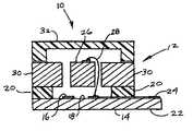
- FIG. 1is a side elevation view, in cross section, showing in schematic form a module in accordance with one embodiment of the invention comprising a MEMS device adhesively bonded to an associated substrate carrying electronic circuitry;
- FIG. 2is a side elevation view, in cross section, of first and second, multi-layer structures which, when combined and processed in accordance with the invention, form an integrated module such as that shown schematically in FIG. 1 ;
- FIG. 3is a side elevation view, in cross section, of the structures of FIG. 2 , adhesively bonded together to form a composite structure;
- FIG. 4is a side elevation view, in cross section, of the composite structure of FIG. 3 after removal of the upper layers of the structure;
- FIG. 5is a side elevation view, in cross section, of the structure of FIG. 4 after substitution of a metal layer for the removed layers;
- FIG. 6is a side elevation view, in cross section, of the structure of FIG. 5 following partial etching defining a MEMS device
- FIG. 7is a side elevation view, in cross section, of the structure of FIG. 6 following release of the MEMS device;
- FIG. 8is a side elevation view, in cross section, of the final integrated module in accordance with the invention.
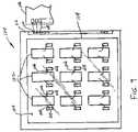
- FIG. 9is a top plan view of a module in accordance with another embodiment of the invention incorporating multiple MEMS devices adhesively bonded to an electronics wafer.
- FIG. 1illustrates, in schematic form, a module 10 in accordance with one embodiment of the present invention.
- the module 10integrates a single MEMS device 12 with a substrate or wafer 14 carrying pre-processed electronic circuitry, shown schematically as a block 16 , occupying an area on an upper surface 18 of the wafer 14 .
- the electronics wafer 14may be in the form of, by way of example, a CMOS die, and the pre-processed circuitry may comprise control, readout/signal conditioning, and/or signal processing circuitry.
- the MEMS device 12is attached to the upper surface of the electronics wafer 14 by means of an adhesive bonding agent 20 , and for compactness overlies at least in part, and preferably in its entirety, the area of the substrate occupied by the electronic circuitry 16 .
- the electronics wafer 14includes an extension 22 projecting beyond the confines of the MEMS device 12 .
- the extension 22carries pads or contacts 24 electrically connected to the circuitry 16 .
- the MEMS device 12may comprise any one of a variety of MEMS sensors and actuators including, without limitation, current sensors, accelerometers, gyros, magnetic sensors, electro-optical actuators, electrical switches, pressure transducers, capacitors and electromechanical motors.
- the MEMS devicecomprises a movable element 26 disposed between a pair of stationary elements 28 .
- the movable MEMS element 26may take various forms depending upon the intended application, for example, a cantilever anchored at one end or a deflectable beam suspended between fixed ends.
- the movable MEMS element 26could comprise the measurement beam of a MEMS current sensor such as that disclosed in U.S. Pat. No. 6,188,322 issued Feb. 13, 2001.
- Electrically conductive connection layers 30 and 32overlie the movable and stationary elements 26 and 28 , respectively.
- the layer 30 on the movable element 26also overlies the fixed anchor or end(s) of the element 26 .
- the conductive layers 30 and 32are electrically coupled to the electronic circuitry 16 on the wafer 14 by means of conductive vias (not shown) extending through the stationary elements 28 and through the fixed anchor or ends of the movable element 26 .
- the conductive layersmay be coupled to the electronic circuitry 16 on the wafer 14 by wire bonds, such as the representative wire bond 34 electrically connecting the conductive layer 32 with a pad 36 on the wafer 14 .
- the upper surfaces of the elements of the MEMS devicemay carry one or more insulating layers and/or electronic circuitry.
- the modulefurther preferably comprises a protective cap or cover 38 appropriately bonded to the top of the MEMS device.
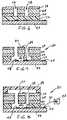
- FIGS. 2 through 8show, in cross-section, the steps for fabricating a module integrating a single MEMS device with a pre-processed electronics wafer, such as, for example, a CMOS die, upon which electronic circuitry has been formed by conventional microcircuitry fabrication techniques.
- the pre-processed circuitrymay comprise, by way of example, control, readout/signal conditioning, and/or signal processing circuitry.
- the process steps shown and described hereinare intended to be generic, being applicable generally to the fabrication of any bulk micromachined MEMS device such as any of those mentioned earlier. Generally, the process exploits the low-temperature nature of the adhesive MEMS process of incorporated U.S. Pat. No. 6,159,385 for compatibility with pre-processed silicon circuitry.
- the first or lower structure 40includes an electronics wafer 44 having an upper surface 46 and a lower surface 47 .
- the upper surface 46carries electronic circuitry represented by a block 48 and electrically conductive interconnections between the circuit elements.
- the electronic circuit elements and their interconnectionsare formed using conventional microfabrication techniques.
- the electronic elementsmay include, without limitation, resistors, inductors, capacitors, transistors, and the like.
- the electronics wafermay comprise a CMOS die.
- Internal wire bond padssuch as the pad 50 , may be formed on the electronics wafer 44 for electrically coupling the circuit elements 48 with the MEMS device to be formed.
- the wafer 44may include a margin 52 that in the final device will define an edge connector or extension carrying external signal, power and ground pads, collectively represented by the pad 54 , electrically connected to the electronic circuitry 48 by means of conductive paths electrically formed on the wafer.
- Alignment marks 55 precisely positioned relative to the circuit elements 48are formed in the upper surface 46 of the wafer 44 .
- Alignment marks 56 corresponding to the marks 55 and in precise vertical alignment therewith,are formed in the lower surface 47 of the wafer 44 .
- An organic adhesive 58is deposited on the upper surface of the wafer 44 .
- Spin coatingprovides the most practical method for application of the organic adhesive although other coating techniques, such as spray coating or the staged deposition of partially cured thin films, may also be used.
- the second or upper layered structure 42comprises a top silicon layer 60 on a thin insulating layer 62 typically having a thickness of 0.25 ⁇ m–2 ⁇ m.
- the insulating layer 62preferably comprises silicon dioxide but, alternatively, may be formed of silicon nitride, aluminum oxide, silicon oxynitride, silicon carbide, or the like.
- the insulating layer 62in turn overlies a silicon layer 64 , typically 10 ⁇ m–80 ⁇ m thick, defining a MEMS device layer.
- the top silicon layer 60which by way of example may be 400 ⁇ m thick, is preferably either a p-type or an n-type silicon such as is commonly used in semiconductor processing; the orientation and the conductivity of the silicon layer 60 will depend on the specific application.
- the silicon MEMS device layer 64is doped so as to impart etch stop and/or semiconductor properties.
- the silicon layer 60comprises a handle layer and this layer, together with the insulating layer 62 , serves as a sacrificial platform for the MEMS device layer 64 .
- the three layers 60 , 62 and 64comprise a silicon-on-insulator (SOI) substrate or wafer commercially available from various suppliers such as Shin-Etsu Handotai Co., Ltd., Japan.
- SOI substratein its commercial form, comprises a buried layer of insulating material, typically silicon dioxide, sandwiched between layers of silicon one of which serves as the handle layer and the other of which comprises the device layer.
- SOI substratesare commercially available having various silicon layer thicknesses and thus may be selected to match the height of the final MEMS device.
- an optional metal layer of aluminum or the like(not shown) may be deposited on the insulating layer 66 .
- An organic adhesive 68is spin coated or otherwise deposited over the MEMS device 64 layer, or over the silicon dioxide and metal layers, if either or both of these are present.
- organic adhesiverefers to thermosetting plastics in which a chemical reaction occurs.
- the chemical reactionincreases rigidity as well as creating a chemical bond with the surfaces being mated.
- While epoxyis the most versatile type of organic adhesive for the present invention, other potential adhesives include polyimides, silicones, acrylics, polyurethanes, polybenzimidazoles, polyquinoralines and benzocyclobutene (BCB).
- Other types of organic adhesivessuch as thermoplastics, which require heating above their melting point like wax, although usable would be of less value for this application.
- the selection of the adhesivedepends in large part on the polymer's thermal characteristics and particularly its glass transition temperature. Other selection criteria include economics, adhesive strength on different substrates, cure shrinkage, environmental compatibility and coefficient of thermal expansion.
- the glass transition temperatureis the temperature at which chemical bonds can freely rotate around the central polymer chain.
- the polymerwhen cured, is a rigid glass-like material.
- the polymerAbove the glass transition, however, the polymer is a softer, elastomeric material.
- CTEcoefficient of thermal expansion
- the adhesive-receiving surfaces of the structures 40 and 42may be exposed to plasma discharge or etching solutions to improve the bonding of the adhesive to such surfaces.
- a coupling agent or adhesion promotersuch as 3-glycidoxy-propyl-trimethoxy-silane (available from Dow Corning as Z-6040) or other agents having long hydrocarbon chains to which the adhesive may bond may be used to improve coating consistency.
- Wetting agentsmay be used to improve coating uniformity.
- the coupling agentmay serve the dual purposes of surface wetting and surface modification.
- surface finishis not overly critical and the surface need not be smooth.
- the first and second structures 40 and 42are positioned in a vacuum chamber (not shown) with the adhesive layers 58 and 68 in confronting relationship.
- the chamberis evacuated to remove air that could be trapped between the first and second structures 40 and 42 during the mating process.
- the first and second structuresare aligned and physically joined with adhesive to form a composite structure 70 ( FIG. 3 ). More specifically, as shown in FIG. 3 , the adhesive layers 58 and 68 combine to form a single adhesive layer 72 bonding together the two module structures 40 and 42 .
- the adhesiveis cured by baking the composite structure for a sequence of oven bakes at elevated temperatures of up to 180° C. to reduce cure shrinkage. As is known, the recommended cure temperatures will depend on the type of adhesive used.
- the bonding of the structuresis followed by a thinning step in which the silicon and silicon dioxide layers 60 and 62 are removed so as to expose an upper surface 73 of the MEMS device layer 64 .
- the layers 60 and 62may be removed using a backside chemical etch.
- a mechanical grinding or polishing stepmay precede the chemical etch to reduce the amount of silicon etching required.
- Alignment marks 74in precise vertical alignment with the marks 56 , are formed in the upper surface 73 of the device layer 64 .
- the removed layersare replaced by an electrically conductive, metal layer 75 having a thickness of about 0.5 to about 3.0 ⁇ m. ( FIG. 5 ).
- the alignment marks 74are visible through the thin layer 75 .
- DRIEdeep reactive ion etching
- one or more insulating layersmay be deposited on the upper surface 73 of the device layer 64 and patterned. Further, stacked insulating layers alternating with metal layers may be formed on the surface 73 , with the metal layers appropriately patterned to define, for example, electrically conductive traces connecting various circuit elements carried by the module. Still further, using known surface micromachining techniques, such layers may be patterned to define a MEMS device such as an electrical switch or other electrical component. In addition, it will be evident that electronic microcircuitry may also be formed on the upper surface 73 of the device layer 64 .
- the adhesive bonding layer 72is then etched to release the MEMS device 80 , that is, to free one or more movable MEMS elements 82 .
- movable elementsmay comprise the displaceable mass of a MEMS accelerometer, the movable plates of a current sensor, and so forth.
- an isotropic, dry oxygen plasma etchis applied to undercut the adhesive layer 72 . ( FIG. 7 .)
- An outer portion of the adhesive layer 72is simultaneously etched away to expose the electrical pads 54 on the margin 52 .
- the circuitry 48 on the wafer 44is then interconnected with the MEMS device 80 by means of plated-through conductive vias or by means of wire bonds 84 (a representative one of which is shown) connected to the internal wire bond pads 50 . Both of these bonding techniques (vias and wire bonding) are well known in the art.
- a protective cap or cover 86is next bonded to the metal layer 75 to complete the fabrication of the MEMS/electronic circuit module shown in FIG. 8 .
- the moduleis then ready to be electrically connected to a higher electronic assembly 88 via conductors 90 attached to the external pads 54 .
- the MEMS device 80overlies at least a portion of the area, and preferably the entire area, occupied by the electronic circuitry 48 on the wafer 44 so as to form a compact module.
- This stacked configurationplaces the MEMS device 80 and the circuitry 48 in close proximity and is made possible by the module fabrication process utilizing low temperature adhesive bonding which does not damage the electronic circuit patterns on the substrate 44 . In the absence of this process, the device 80 would have to be bonded to the substrate 44 at a location remote from the region occupied by the electronic circuitry.
- FIG. 9there is shown in schematic form an alternative embodiment of the invention comprising a module 100 incorporating multiple—in this case nine—MEMS devices 102 adhesively attached to a substrate 104 comprising, for example, a CMOS wafer which may have one or more regions on the upper surface with electronic circuitry patterned thereon.
- the MEMS devices 102may all be of the same type or may comprise different types.
- wire bonds 106(or alternatively, plated-through, conductive vias) connect the MEMS devices 102 to the electronic circuitry on the wafer by means of pads 108 .
- the wafer circuitryis in turn connected to contacts 110 on an extension 112 of the wafer 104 .
- a protective cover 114overlies the MEMS devices 102 .
- the module 100may be coupled to a higher circuit assembly 116 by electrical conductors 118 connected to the contacts 110 .
- the module 100is fabricated using the process steps described in connection with FIGS. 2–8 .
Landscapes
- Engineering & Computer Science (AREA)
- Power Engineering (AREA)
- Microelectronics & Electronic Packaging (AREA)
- Manufacturing & Machinery (AREA)
- Micromachines (AREA)
Abstract
Description
Claims (13)
Priority Applications (1)
| Application Number | Priority Date | Filing Date | Title |
|---|---|---|---|
| US10/438,512US6979872B2 (en) | 2003-05-13 | 2003-05-13 | Modules integrating MEMS devices with pre-processed electronic circuitry, and methods for fabricating such modules |
Applications Claiming Priority (1)
| Application Number | Priority Date | Filing Date | Title |
|---|---|---|---|
| US10/438,512US6979872B2 (en) | 2003-05-13 | 2003-05-13 | Modules integrating MEMS devices with pre-processed electronic circuitry, and methods for fabricating such modules |
Publications (2)
| Publication Number | Publication Date |
|---|---|
| US20040227201A1 US20040227201A1 (en) | 2004-11-18 |
| US6979872B2true US6979872B2 (en) | 2005-12-27 |
Family
ID=33417594
Family Applications (1)
| Application Number | Title | Priority Date | Filing Date |
|---|---|---|---|
| US10/438,512Expired - LifetimeUS6979872B2 (en) | 2003-05-13 | 2003-05-13 | Modules integrating MEMS devices with pre-processed electronic circuitry, and methods for fabricating such modules |
Country Status (1)
| Country | Link |
|---|---|
| US (1) | US6979872B2 (en) |
Cited By (37)
| Publication number | Priority date | Publication date | Assignee | Title |
|---|---|---|---|---|
| US20060131714A1 (en)* | 2004-12-17 | 2006-06-22 | Picciotto Carl E | Signal conduction for doped semiconductors |
| US20080072173A1 (en)* | 2002-07-10 | 2008-03-20 | Ralph Brunner | Method and apparatus for resizing buffered windows |
| US20090057789A1 (en)* | 2007-09-05 | 2009-03-05 | Long-Sun Huang | Package structure for micro-sensor |
| US20090115046A1 (en)* | 2007-10-17 | 2009-05-07 | Pixart Imaging Incorporation | Micro-electro-mechanical system device and method for making same |
| US20100312468A1 (en)* | 2009-06-03 | 2010-12-09 | Honeywell International Inc. | Integrated micro-electro-mechanical systems (mems) sensor device |
| US20110005326A1 (en)* | 2009-07-10 | 2011-01-13 | Honeywell International Inc. | Sensor package assembly having an unconstrained sense die |
| WO2011080409A2 (en) | 2009-12-15 | 2011-07-07 | Commissariat A L'energie Atomique Et Aux Energies Alternatives | Process for fabricating an electronic component combining an electromechanical system and an electronic circuit |
| US8138008B1 (en)* | 2010-11-29 | 2012-03-20 | International Business Machines Corporation | Forming an oxide MEMS beam |
| US8230743B2 (en) | 2010-08-23 | 2012-07-31 | Honeywell International Inc. | Pressure sensor |
| US8236577B1 (en) | 2010-01-15 | 2012-08-07 | MCube Inc. | Foundry compatible process for manufacturing a magneto meter using lorentz force for integrated systems |
| US8367522B1 (en) | 2010-04-08 | 2013-02-05 | MCube Inc. | Method and structure of integrated micro electro-mechanical systems and electronic devices using edge bond pads |
| US8395252B1 (en)* | 2009-11-13 | 2013-03-12 | MCube Inc. | Integrated MEMS and CMOS package and method |
| US8407905B1 (en) | 2010-01-15 | 2013-04-02 | Mcube, Inc. | Multiple magneto meters using Lorentz force for integrated systems |
| US8421082B1 (en)* | 2010-01-19 | 2013-04-16 | Mcube, Inc. | Integrated CMOS and MEMS with air dielectric method and system |
| US8477473B1 (en) | 2010-08-19 | 2013-07-02 | MCube Inc. | Transducer structure and method for MEMS devices |
| US8476129B1 (en) | 2010-05-24 | 2013-07-02 | MCube Inc. | Method and structure of sensors and MEMS devices using vertical mounting with interconnections |
| US8476084B1 (en) | 2010-05-24 | 2013-07-02 | MCube Inc. | Method and structure of sensors or electronic devices using vertical mounting |
| US8486723B1 (en) | 2010-08-19 | 2013-07-16 | MCube Inc. | Three axis magnetic sensor device and method |
| US8553389B1 (en) | 2010-08-19 | 2013-10-08 | MCube Inc. | Anchor design and method for MEMS transducer apparatuses |
| US8584521B1 (en) | 2010-01-19 | 2013-11-19 | MCube Inc. | Accurate gyroscope device using MEMS and quartz |
| US8637943B1 (en) | 2010-01-04 | 2014-01-28 | MCube Inc. | Multi-axis integrated MEMS devices with CMOS circuits and method therefor |
| US8652961B1 (en)* | 2010-06-18 | 2014-02-18 | MCube Inc. | Methods and structure for adapting MEMS structures to form electrical interconnections for integrated circuits |
| US8710597B1 (en) | 2010-04-21 | 2014-04-29 | MCube Inc. | Method and structure for adding mass with stress isolation to MEMS structures |
| US8723986B1 (en) | 2010-11-04 | 2014-05-13 | MCube Inc. | Methods and apparatus for initiating image capture on a hand-held device |
| US8794065B1 (en) | 2010-02-27 | 2014-08-05 | MCube Inc. | Integrated inertial sensing apparatus using MEMS and quartz configured on crystallographic planes |
| US8797279B2 (en) | 2010-05-25 | 2014-08-05 | MCube Inc. | Analog touchscreen methods and apparatus |
| US8823007B2 (en) | 2009-10-28 | 2014-09-02 | MCube Inc. | Integrated system on chip using multiple MEMS and CMOS devices |
| US8869616B1 (en) | 2010-06-18 | 2014-10-28 | MCube Inc. | Method and structure of an inertial sensor using tilt conversion |
| US8928696B1 (en) | 2010-05-25 | 2015-01-06 | MCube Inc. | Methods and apparatus for operating hysteresis on a hand held device |
| US8928602B1 (en) | 2009-03-03 | 2015-01-06 | MCube Inc. | Methods and apparatus for object tracking on a hand-held device |
| US8936959B1 (en) | 2010-02-27 | 2015-01-20 | MCube Inc. | Integrated rf MEMS, control systems and methods |
| US8969101B1 (en) | 2011-08-17 | 2015-03-03 | MCube Inc. | Three axis magnetic sensor device and method using flex cables |
| US8993362B1 (en) | 2010-07-23 | 2015-03-31 | MCube Inc. | Oxide retainer method for MEMS devices |
| CN108910819A (en)* | 2018-07-13 | 2018-11-30 | 河南汇纳科技有限公司 | A kind of three-dimensionally integrated method of multisensor that MEMS is compatible |
| US10213107B2 (en) | 2014-07-01 | 2019-02-26 | Injectsense, Inc. | Methods and devices for implantation of intraocular pressure sensors |
| US10973425B2 (en) | 2014-07-01 | 2021-04-13 | Injectsense, Inc. | Hermetically sealed implant sensors with vertical stacking architecture |
| US11846597B2 (en) | 2018-01-03 | 2023-12-19 | Corning Incorporated | Methods for making electrodes and providing electrical connections in sensors |
Families Citing this family (29)
| Publication number | Priority date | Publication date | Assignee | Title |
|---|---|---|---|---|
| JP4441974B2 (en)* | 2000-03-24 | 2010-03-31 | ソニー株式会社 | Manufacturing method of semiconductor device |
| KR101335163B1 (en)* | 2004-03-15 | 2013-12-02 | 조지아 테크 리서치 코오포레이션 | Packaging for micro electro-mechanical systems and methods of fabricating thereof |
| KR100846569B1 (en)* | 2006-06-14 | 2008-07-15 | 매그나칩 반도체 유한회사 | Package of MEMS element and manufacturing method thereof |
| US8462109B2 (en) | 2007-01-05 | 2013-06-11 | Invensense, Inc. | Controlling and accessing content using motion processing on mobile devices |
| US7934423B2 (en) | 2007-12-10 | 2011-05-03 | Invensense, Inc. | Vertically integrated 3-axis MEMS angular accelerometer with integrated electronics |
| US8952832B2 (en) | 2008-01-18 | 2015-02-10 | Invensense, Inc. | Interfacing application programs and motion sensors of a device |
| US8141424B2 (en) | 2008-09-12 | 2012-03-27 | Invensense, Inc. | Low inertia frame for detecting coriolis acceleration |
| US8250921B2 (en) | 2007-07-06 | 2012-08-28 | Invensense, Inc. | Integrated motion processing unit (MPU) with MEMS inertial sensing and embedded digital electronics |
| TWI340121B (en)* | 2007-12-14 | 2011-04-11 | Memsmart Semiconductor Corp | A micro suspended structure and its manufacturing method |
| US7851875B2 (en) | 2008-01-11 | 2010-12-14 | Infineon Technologies Ag | MEMS devices and methods of manufacture thereof |
| US8125046B2 (en) | 2008-06-04 | 2012-02-28 | Infineon Technologies Ag | Micro-electromechanical system devices |
| JP2010044964A (en)* | 2008-08-13 | 2010-02-25 | Toshiba Corp | Micro movable device |
| US9709509B1 (en) | 2009-11-13 | 2017-07-18 | MCube Inc. | System configured for integrated communication, MEMS, Processor, and applications using a foundry compatible semiconductor process |
| US8402666B1 (en) | 2009-11-30 | 2013-03-26 | Mcube, Inc. | Magneto meter using lorentz force for integrated systems |
| US8564075B1 (en) | 2010-04-21 | 2013-10-22 | MCube Inc. | Package tolerate design and method |
| US8643612B2 (en)* | 2010-05-25 | 2014-02-04 | MCube Inc. | Touchscreen operation threshold methods and apparatus |
| EP2426083A3 (en)* | 2010-09-03 | 2013-11-13 | Domintech Co., LTD. | Mems sensor package |
| CN102398885A (en)* | 2010-09-14 | 2012-04-04 | 利顺精密科技股份有限公司 | Micro-electromechanical sensor device |
| US9276080B2 (en)* | 2012-03-09 | 2016-03-01 | Mcube, Inc. | Methods and structures of integrated MEMS-CMOS devices |
| US9540232B2 (en) | 2010-11-12 | 2017-01-10 | MCube Inc. | Method and structure of MEMS WLCSP fabrication |
| US9278853B2 (en)* | 2011-03-28 | 2016-03-08 | Miramems Sensing Technology Co., Ltd. | Manufacturing process of MEMS device |
| US9778039B2 (en)* | 2011-10-31 | 2017-10-03 | The Regents Of The University Of Michigan | Microsystem device and methods for fabricating the same |
| US8673670B2 (en) | 2011-12-15 | 2014-03-18 | International Business Machines Corporation | Micro-electro-mechanical system (MEMS) structures and design structures |
| US10913653B2 (en) | 2013-03-07 | 2021-02-09 | MCube Inc. | Method of fabricating MEMS devices using plasma etching and device therefor |
| SG10201408532SA (en)* | 2013-12-19 | 2015-07-30 | Agency Science Tech & Res | Method For Thin Film Encapsulation (TFE) Of A Microelectromechanical System (MEMS) Device And The MEMS Device Encapsulated Thereof |
| US9796580B2 (en) | 2015-06-12 | 2017-10-24 | Invensense, Inc. | CMOS-MEMS-CMOS platform |
| US9731961B2 (en) | 2015-07-10 | 2017-08-15 | Invensense, Inc. | MEMS-CMOS-MEMS platform |
| US9758367B2 (en)* | 2015-12-09 | 2017-09-12 | Analog Devices, Inc. | Metallizing MEMS devices |
| DE102017114085B4 (en) | 2016-06-28 | 2023-05-04 | Analog Devices, Inc. | Selective conductive coating for MEMS sensors |
Citations (18)
| Publication number | Priority date | Publication date | Assignee | Title |
|---|---|---|---|---|
| US4874499A (en)* | 1988-05-23 | 1989-10-17 | Massachusetts Institute Of Technology | Electrochemical microsensors and method of making such sensors |
| US5578976A (en) | 1995-06-22 | 1996-11-26 | Rockwell International Corporation | Micro electromechanical RF switch |
| US5880921A (en) | 1997-04-28 | 1999-03-09 | Rockwell Science Center, Llc | Monolithically integrated switched capacitor bank using micro electro mechanical system (MEMS) technology |
| US5959516A (en) | 1998-01-08 | 1999-09-28 | Rockwell Science Center, Llc | Tunable-trimmable micro electro mechanical system (MEMS) capacitor |
| US6074890A (en) | 1998-01-08 | 2000-06-13 | Rockwell Science Center, Llc | Method of fabricating suspended single crystal silicon micro electro mechanical system (MEMS) devices |
| US6159385A (en) | 1998-05-08 | 2000-12-12 | Rockwell Technologies, Llc | Process for manufacture of micro electromechanical devices having high electrical isolation |
| US6188322B1 (en) | 1999-09-28 | 2001-02-13 | Rockwell Technologies, Llc | Method for sensing electrical current |
| US6199874B1 (en) | 1993-05-26 | 2001-03-13 | Cornell Research Foundation Inc. | Microelectromechanical accelerometer for automotive applications |
| US6275122B1 (en) | 1999-08-17 | 2001-08-14 | International Business Machines Corporation | Encapsulated MEMS band-pass filter for integrated circuits |
| US6277666B1 (en) | 1999-06-24 | 2001-08-21 | Honeywell Inc. | Precisely defined microelectromechanical structures and associated fabrication methods |
| US6348788B1 (en) | 1999-09-28 | 2002-02-19 | Rockwell Automation Technologies, Inc. | High resolution current sensing apparatus |
| US6417743B1 (en) | 1999-09-21 | 2002-07-09 | Rockwell Science Center, Llc | Micro electromechanical isolator |
| US6423815B1 (en)* | 1999-08-30 | 2002-07-23 | Sumitomo Bakelite Company, Limited | Layer insulating film for multilayer interconnection, resin used therefor and process for producing the same |
| US20030174934A1 (en)* | 2002-03-15 | 2003-09-18 | Hiromu Ishii | Optical switch device |
| US20040016995A1 (en)* | 2002-07-25 | 2004-01-29 | Kuo Shun Meen | MEMS control chip integration |
| US20040063237A1 (en)* | 2002-09-27 | 2004-04-01 | Chang-Han Yun | Fabricating complex micro-electromechanical systems using a dummy handling substrate |
| US20040076366A1 (en)* | 2002-10-18 | 2004-04-22 | Chang-Han Yun | Fiber-attached optical devices with in-plane micromachined mirrors |
| US20040112529A1 (en)* | 2002-10-09 | 2004-06-17 | Cellectricon Ab | Methods for interfacing macroscale components to microscale devices |
- 2003
- 2003-05-13USUS10/438,512patent/US6979872B2/ennot_activeExpired - Lifetime
Patent Citations (19)
| Publication number | Priority date | Publication date | Assignee | Title |
|---|---|---|---|---|
| US4874499A (en)* | 1988-05-23 | 1989-10-17 | Massachusetts Institute Of Technology | Electrochemical microsensors and method of making such sensors |
| US6199874B1 (en) | 1993-05-26 | 2001-03-13 | Cornell Research Foundation Inc. | Microelectromechanical accelerometer for automotive applications |
| US5578976A (en) | 1995-06-22 | 1996-11-26 | Rockwell International Corporation | Micro electromechanical RF switch |
| US5880921A (en) | 1997-04-28 | 1999-03-09 | Rockwell Science Center, Llc | Monolithically integrated switched capacitor bank using micro electro mechanical system (MEMS) technology |
| US5959516A (en) | 1998-01-08 | 1999-09-28 | Rockwell Science Center, Llc | Tunable-trimmable micro electro mechanical system (MEMS) capacitor |
| US6074890A (en) | 1998-01-08 | 2000-06-13 | Rockwell Science Center, Llc | Method of fabricating suspended single crystal silicon micro electro mechanical system (MEMS) devices |
| US6159385A (en) | 1998-05-08 | 2000-12-12 | Rockwell Technologies, Llc | Process for manufacture of micro electromechanical devices having high electrical isolation |
| US6277666B1 (en) | 1999-06-24 | 2001-08-21 | Honeywell Inc. | Precisely defined microelectromechanical structures and associated fabrication methods |
| US6275122B1 (en) | 1999-08-17 | 2001-08-14 | International Business Machines Corporation | Encapsulated MEMS band-pass filter for integrated circuits |
| US6423815B1 (en)* | 1999-08-30 | 2002-07-23 | Sumitomo Bakelite Company, Limited | Layer insulating film for multilayer interconnection, resin used therefor and process for producing the same |
| US6417743B1 (en) | 1999-09-21 | 2002-07-09 | Rockwell Science Center, Llc | Micro electromechanical isolator |
| US6188322B1 (en) | 1999-09-28 | 2001-02-13 | Rockwell Technologies, Llc | Method for sensing electrical current |
| US6348788B1 (en) | 1999-09-28 | 2002-02-19 | Rockwell Automation Technologies, Inc. | High resolution current sensing apparatus |
| US6411214B1 (en) | 1999-09-28 | 2002-06-25 | Rockwell Automation Technologies, Inc. | Method for sensing electrical current |
| US20030174934A1 (en)* | 2002-03-15 | 2003-09-18 | Hiromu Ishii | Optical switch device |
| US20040016995A1 (en)* | 2002-07-25 | 2004-01-29 | Kuo Shun Meen | MEMS control chip integration |
| US20040063237A1 (en)* | 2002-09-27 | 2004-04-01 | Chang-Han Yun | Fabricating complex micro-electromechanical systems using a dummy handling substrate |
| US20040112529A1 (en)* | 2002-10-09 | 2004-06-17 | Cellectricon Ab | Methods for interfacing macroscale components to microscale devices |
| US20040076366A1 (en)* | 2002-10-18 | 2004-04-22 | Chang-Han Yun | Fiber-attached optical devices with in-plane micromachined mirrors |
Non-Patent Citations (2)
| Title |
|---|
| M. Heschel et al., "Stacking Technology for A Space Constrained Microsystem", IEEE, 11th Annual International Workshop on Micro Electrical Mechanical Systems, Jan. 25-29, 1998, pp. 312-317.* |
| Merriam-Webster's Collegiate Dictionary, 10ed., 2001, pp. 817.* |
Cited By (50)
| Publication number | Priority date | Publication date | Assignee | Title |
|---|---|---|---|---|
| US20080072173A1 (en)* | 2002-07-10 | 2008-03-20 | Ralph Brunner | Method and apparatus for resizing buffered windows |
| US20060131714A1 (en)* | 2004-12-17 | 2006-06-22 | Picciotto Carl E | Signal conduction for doped semiconductors |
| US7521784B2 (en)* | 2004-12-17 | 2009-04-21 | Hewlett-Packard Development Company, L.P. | System for coupling wire to semiconductor region |
| US20090057789A1 (en)* | 2007-09-05 | 2009-03-05 | Long-Sun Huang | Package structure for micro-sensor |
| US20090115046A1 (en)* | 2007-10-17 | 2009-05-07 | Pixart Imaging Incorporation | Micro-electro-mechanical system device and method for making same |
| US7759256B2 (en)* | 2007-10-17 | 2010-07-20 | Pixart Imaging Incorporation | Micro-electro-mechanical system device and method for making same |
| US8928602B1 (en) | 2009-03-03 | 2015-01-06 | MCube Inc. | Methods and apparatus for object tracking on a hand-held device |
| US20100312468A1 (en)* | 2009-06-03 | 2010-12-09 | Honeywell International Inc. | Integrated micro-electro-mechanical systems (mems) sensor device |
| US8315793B2 (en) | 2009-06-03 | 2012-11-20 | Honeywell International Inc. | Integrated micro-electro-mechanical systems (MEMS) sensor device |
| US9321629B2 (en) | 2009-06-23 | 2016-04-26 | MCube Inc. | Method and structure for adding mass with stress isolation to MEMS structures |
| US9365412B2 (en)* | 2009-06-23 | 2016-06-14 | MCube Inc. | Integrated CMOS and MEMS devices with air dieletrics |
| US8981560B2 (en) | 2009-06-23 | 2015-03-17 | MCube Inc. | Method and structure of sensors and MEMS devices using vertical mounting with interconnections |
| US8322225B2 (en) | 2009-07-10 | 2012-12-04 | Honeywell International Inc. | Sensor package assembly having an unconstrained sense die |
| US20110005326A1 (en)* | 2009-07-10 | 2011-01-13 | Honeywell International Inc. | Sensor package assembly having an unconstrained sense die |
| US8823007B2 (en) | 2009-10-28 | 2014-09-02 | MCube Inc. | Integrated system on chip using multiple MEMS and CMOS devices |
| US8395252B1 (en)* | 2009-11-13 | 2013-03-12 | MCube Inc. | Integrated MEMS and CMOS package and method |
| WO2011080409A2 (en) | 2009-12-15 | 2011-07-07 | Commissariat A L'energie Atomique Et Aux Energies Alternatives | Process for fabricating an electronic component combining an electromechanical system and an electronic circuit |
| US9150406B2 (en) | 2010-01-04 | 2015-10-06 | MCube Inc. | Multi-axis integrated MEMS devices with CMOS circuits and method therefor |
| US8637943B1 (en) | 2010-01-04 | 2014-01-28 | MCube Inc. | Multi-axis integrated MEMS devices with CMOS circuits and method therefor |
| US8236577B1 (en) | 2010-01-15 | 2012-08-07 | MCube Inc. | Foundry compatible process for manufacturing a magneto meter using lorentz force for integrated systems |
| US8407905B1 (en) | 2010-01-15 | 2013-04-02 | Mcube, Inc. | Multiple magneto meters using Lorentz force for integrated systems |
| US8584521B1 (en) | 2010-01-19 | 2013-11-19 | MCube Inc. | Accurate gyroscope device using MEMS and quartz |
| US8421082B1 (en)* | 2010-01-19 | 2013-04-16 | Mcube, Inc. | Integrated CMOS and MEMS with air dielectric method and system |
| US8794065B1 (en) | 2010-02-27 | 2014-08-05 | MCube Inc. | Integrated inertial sensing apparatus using MEMS and quartz configured on crystallographic planes |
| US8936959B1 (en) | 2010-02-27 | 2015-01-20 | MCube Inc. | Integrated rf MEMS, control systems and methods |
| US8367522B1 (en) | 2010-04-08 | 2013-02-05 | MCube Inc. | Method and structure of integrated micro electro-mechanical systems and electronic devices using edge bond pads |
| US8592993B2 (en) | 2010-04-08 | 2013-11-26 | MCube Inc. | Method and structure of integrated micro electro-mechanical systems and electronic devices using edge bond pads |
| US8710597B1 (en) | 2010-04-21 | 2014-04-29 | MCube Inc. | Method and structure for adding mass with stress isolation to MEMS structures |
| US8476129B1 (en) | 2010-05-24 | 2013-07-02 | MCube Inc. | Method and structure of sensors and MEMS devices using vertical mounting with interconnections |
| US8476084B1 (en) | 2010-05-24 | 2013-07-02 | MCube Inc. | Method and structure of sensors or electronic devices using vertical mounting |
| US8797279B2 (en) | 2010-05-25 | 2014-08-05 | MCube Inc. | Analog touchscreen methods and apparatus |
| US8928696B1 (en) | 2010-05-25 | 2015-01-06 | MCube Inc. | Methods and apparatus for operating hysteresis on a hand held device |
| US8652961B1 (en)* | 2010-06-18 | 2014-02-18 | MCube Inc. | Methods and structure for adapting MEMS structures to form electrical interconnections for integrated circuits |
| US8869616B1 (en) | 2010-06-18 | 2014-10-28 | MCube Inc. | Method and structure of an inertial sensor using tilt conversion |
| US8993362B1 (en) | 2010-07-23 | 2015-03-31 | MCube Inc. | Oxide retainer method for MEMS devices |
| US9376312B2 (en) | 2010-08-19 | 2016-06-28 | MCube Inc. | Method for fabricating a transducer apparatus |
| US9377487B2 (en) | 2010-08-19 | 2016-06-28 | MCube Inc. | Transducer structure and method for MEMS devices |
| US8477473B1 (en) | 2010-08-19 | 2013-07-02 | MCube Inc. | Transducer structure and method for MEMS devices |
| US8553389B1 (en) | 2010-08-19 | 2013-10-08 | MCube Inc. | Anchor design and method for MEMS transducer apparatuses |
| US8486723B1 (en) | 2010-08-19 | 2013-07-16 | MCube Inc. | Three axis magnetic sensor device and method |
| US8230743B2 (en) | 2010-08-23 | 2012-07-31 | Honeywell International Inc. | Pressure sensor |
| US8723986B1 (en) | 2010-11-04 | 2014-05-13 | MCube Inc. | Methods and apparatus for initiating image capture on a hand-held device |
| US8138008B1 (en)* | 2010-11-29 | 2012-03-20 | International Business Machines Corporation | Forming an oxide MEMS beam |
| US8969101B1 (en) | 2011-08-17 | 2015-03-03 | MCube Inc. | Three axis magnetic sensor device and method using flex cables |
| US10213107B2 (en) | 2014-07-01 | 2019-02-26 | Injectsense, Inc. | Methods and devices for implantation of intraocular pressure sensors |
| US10973425B2 (en) | 2014-07-01 | 2021-04-13 | Injectsense, Inc. | Hermetically sealed implant sensors with vertical stacking architecture |
| US11202568B2 (en) | 2014-07-01 | 2021-12-21 | Injectsense, Inc. | Methods and devices for implantation of intraocular pressure sensors |
| US11846597B2 (en) | 2018-01-03 | 2023-12-19 | Corning Incorporated | Methods for making electrodes and providing electrical connections in sensors |
| US12222308B2 (en) | 2018-01-03 | 2025-02-11 | Corning Incorporated | Methods for making electrodes and providing electrical connections in sensors |
| CN108910819A (en)* | 2018-07-13 | 2018-11-30 | 河南汇纳科技有限公司 | A kind of three-dimensionally integrated method of multisensor that MEMS is compatible |
Also Published As
| Publication number | Publication date |
|---|---|
| US20040227201A1 (en) | 2004-11-18 |
Similar Documents
| Publication | Publication Date | Title |
|---|---|---|
| US6979872B2 (en) | Modules integrating MEMS devices with pre-processed electronic circuitry, and methods for fabricating such modules | |
| US7247246B2 (en) | Vertical integration of a MEMS structure with electronics in a hermetically sealed cavity | |
| US6159385A (en) | Process for manufacture of micro electromechanical devices having high electrical isolation | |
| US7104129B2 (en) | Vertically integrated MEMS structure with electronics in a hermetically sealed cavity | |
| US6894358B2 (en) | Process for producing microelectromechanical components and a housed microelectromechanical component | |
| US8710599B2 (en) | Micromachined devices and fabricating the same | |
| US7083997B2 (en) | Bonded wafer optical MEMS process | |
| US7989248B2 (en) | Method of forming monolithic CMOS-MEMS hybrid integrated, packaged structures | |
| US20110027941A1 (en) | Method of forming monolithic cmos-mems hybrid integrated, packaged structures | |
| US8685776B2 (en) | Wafer level packaged MEMS device | |
| Niklaus et al. | Low-temperature wafer-level transfer bonding | |
| US10913093B2 (en) | Micro-electro-mechanical system piezoelectric transducer and method for manufacturing the same | |
| US20100252897A1 (en) | Performance-enhancing two-sided mems anchor design for vertically integrated micromachined devices | |
| US8101469B2 (en) | Method of forming monolithic CMOS-MEMS hybrid integrated, packaged structures | |
| CN108862185B (en) | Method of manufacturing wafer-level packaged MEMS component and MEMS component | |
| US7618837B2 (en) | Method for fabricating high aspect ratio MEMS device with integrated circuit on the same substrate using post-CMOS process | |
| US7531424B1 (en) | Vacuum wafer-level packaging for SOI-MEMS devices | |
| US11267697B2 (en) | Use of an uncoupling structure for assembling a component having a casing | |
| US8115265B2 (en) | Interconnection system on a plane adjacent to a solid-state device structure | |
| KR100324716B1 (en) | Packaging Methods for Microstructures and Microsystems | |
| US20120126351A1 (en) | Interconnection system on a plane adjacent to a solid-state device structure | |
| EP1428249A1 (en) | Bonding method | |
| JP2014206535A (en) | Method of forming wafer level packaged device |
Legal Events
| Date | Code | Title | Description |
|---|---|---|---|
| AS | Assignment | Owner name:INNOVATIVE TECHNOLOGY LICENSING LLC, CALIFORNIA Free format text:ASSIGNMENT OF ASSIGNORS INTEREST;ASSIGNORS:BORWICK, III, ROBERT L.;DENATALE, JEFFREY F.;ANDERSON, ROBERT J.;REEL/FRAME:014085/0718 Effective date:20030512 | |
| STCF | Information on status: patent grant | Free format text:PATENTED CASE | |
| AS | Assignment | Owner name:TELEDYNE LICENSING, LLC, CALIFORNIA Free format text:CHANGE OF NAME;ASSIGNOR:ROCKWELL SCIENTIFIC LICENSING, LLC;REEL/FRAME:018573/0660 Effective date:20060918 Owner name:ROCKWELL SCIENTIFIC LICENSING, LLC, CALIFORNIA Free format text:CHANGE OF NAME;ASSIGNOR:INNOVATIVE TECHNOLOGY LICENSING, LLC;REEL/FRAME:018573/0657 Effective date:20030919 | |
| CC | Certificate of correction | ||
| CC | Certificate of correction | ||
| FEPP | Fee payment procedure | Free format text:PAYER NUMBER DE-ASSIGNED (ORIGINAL EVENT CODE: RMPN); ENTITY STATUS OF PATENT OWNER: LARGE ENTITY Free format text:PAYOR NUMBER ASSIGNED (ORIGINAL EVENT CODE: ASPN); ENTITY STATUS OF PATENT OWNER: LARGE ENTITY | |
| FPAY | Fee payment | Year of fee payment:4 | |
| AS | Assignment | Owner name:TELEDYNE SCIENTIFIC & IMAGING, LLC, CALIFORNIA Free format text:MERGER;ASSIGNOR:TELEDYNE LICENSING, LLC;REEL/FRAME:027830/0206 Effective date:20111221 | |
| FPAY | Fee payment | Year of fee payment:8 | |
| FPAY | Fee payment | Year of fee payment:12 |