US6979849B2 - Memory cell having improved interconnect - Google Patents
Memory cell having improved interconnectDownload PDFInfo
- Publication number
- US6979849B2 US6979849B2US10/750,737US75073703AUS6979849B2US 6979849 B2US6979849 B2US 6979849B2US 75073703 AUS75073703 AUS 75073703AUS 6979849 B2US6979849 B2US 6979849B2
- Authority
- US
- United States
- Prior art keywords
- transistor
- cell plate
- set forth
- memory device
- conductive
- Prior art date
- Legal status (The legal status is an assumption and is not a legal conclusion. Google has not performed a legal analysis and makes no representation as to the accuracy of the status listed.)
- Expired - Fee Related, expires
Links
- 239000003990capacitorSubstances0.000claimsabstractdescription37
- 238000003860storageMethods0.000claimsabstractdescription34
- 239000000463materialSubstances0.000claimsdescription15
- 229910021420polycrystalline siliconInorganic materials0.000claimsdescription11
- 229920005591polysiliconPolymers0.000claimsdescription11
- WFKWXMTUELFFGS-UHFFFAOYSA-NtungstenChemical compound[W]WFKWXMTUELFFGS-UHFFFAOYSA-N0.000claimsdescription7
- 229910052721tungstenInorganic materials0.000claimsdescription7
- 239000010937tungstenSubstances0.000claimsdescription7
- 229910052751metalInorganic materials0.000claimsdescription6
- 239000002184metalSubstances0.000claimsdescription6
- 238000000034methodMethods0.000description21
- 238000004519manufacturing processMethods0.000description12
- 230000008569processEffects0.000description11
- 239000000758substrateSubstances0.000description11
- 230000006870functionEffects0.000description7
- 238000013461designMethods0.000description5
- 239000003989dielectric materialSubstances0.000description5
- 238000000059patterningMethods0.000description4
- 239000005360phosphosilicate glassSubstances0.000description4
- 230000015572biosynthetic processEffects0.000description3
- 238000010586diagramMethods0.000description3
- XUIMIQQOPSSXEZ-UHFFFAOYSA-NSiliconChemical compound[Si]XUIMIQQOPSSXEZ-UHFFFAOYSA-N0.000description2
- NRTOMJZYCJJWKI-UHFFFAOYSA-NTitanium nitrideChemical compound[Ti]#NNRTOMJZYCJJWKI-UHFFFAOYSA-N0.000description2
- 230000008901benefitEffects0.000description2
- 238000005229chemical vapour depositionMethods0.000description2
- 238000004891communicationMethods0.000description2
- 239000004020conductorSubstances0.000description2
- 238000011161developmentMethods0.000description2
- 239000002019doping agentSubstances0.000description2
- 238000005516engineering processMethods0.000description2
- 238000005468ion implantationMethods0.000description2
- 238000012986modificationMethods0.000description2
- 230000004048modificationEffects0.000description2
- 150000004767nitridesChemical class0.000description2
- TWNQGVIAIRXVLR-UHFFFAOYSA-Noxo(oxoalumanyloxy)alumaneChemical compoundO=[Al]O[Al]=OTWNQGVIAIRXVLR-UHFFFAOYSA-N0.000description2
- 230000002093peripheral effectEffects0.000description2
- 238000005240physical vapour depositionMethods0.000description2
- 238000012545processingMethods0.000description2
- 239000004065semiconductorSubstances0.000description2
- 229910052710siliconInorganic materials0.000description2
- 239000010703siliconSubstances0.000description2
- 125000006850spacer groupChemical group0.000description2
- 230000003068static effectEffects0.000description2
- ZOXJGFHDIHLPTG-UHFFFAOYSA-NBoronChemical compound[B]ZOXJGFHDIHLPTG-UHFFFAOYSA-N0.000description1
- 229910052796boronInorganic materials0.000description1
- 230000001413cellular effectEffects0.000description1
- 235000019504cigarettesNutrition0.000description1
- 230000008878couplingEffects0.000description1
- 238000010168coupling processMethods0.000description1
- 238000005859coupling reactionMethods0.000description1
- 238000000151depositionMethods0.000description1
- 230000008021depositionEffects0.000description1
- 238000005137deposition processMethods0.000description1
- 238000009792diffusion processMethods0.000description1
- 238000005530etchingMethods0.000description1
- CWAFVXWRGIEBPL-UHFFFAOYSA-NethoxysilaneChemical compoundCCO[SiH3]CWAFVXWRGIEBPL-UHFFFAOYSA-N0.000description1
- 238000010438heat treatmentMethods0.000description1
- 230000014759maintenance of locationEffects0.000description1
- 230000003647oxidationEffects0.000description1
- 238000007254oxidation reactionMethods0.000description1
- 238000004080punchingMethods0.000description1
- WQJQOUPTWCFRMM-UHFFFAOYSA-Ntungsten disilicideChemical compound[Si]#[W]#[Si]WQJQOUPTWCFRMM-UHFFFAOYSA-N0.000description1
- 229910021342tungsten silicideInorganic materials0.000description1
Images


Classifications
- H—ELECTRICITY
- H10—SEMICONDUCTOR DEVICES; ELECTRIC SOLID-STATE DEVICES NOT OTHERWISE PROVIDED FOR
- H10B—ELECTRONIC MEMORY DEVICES
- H10B12/00—Dynamic random access memory [DRAM] devices
- H10B12/01—Manufacture or treatment
- H10B12/09—Manufacture or treatment with simultaneous manufacture of the peripheral circuit region and memory cells
- G—PHYSICS
- G11—INFORMATION STORAGE
- G11C—STATIC STORES
- G11C11/00—Digital stores characterised by the use of particular electric or magnetic storage elements; Storage elements therefor
- G11C11/21—Digital stores characterised by the use of particular electric or magnetic storage elements; Storage elements therefor using electric elements
- G11C11/34—Digital stores characterised by the use of particular electric or magnetic storage elements; Storage elements therefor using electric elements using semiconductor devices
- G11C11/40—Digital stores characterised by the use of particular electric or magnetic storage elements; Storage elements therefor using electric elements using semiconductor devices using transistors
- G11C11/401—Digital stores characterised by the use of particular electric or magnetic storage elements; Storage elements therefor using electric elements using semiconductor devices using transistors forming cells needing refreshing or charge regeneration, i.e. dynamic cells
- G11C11/403—Digital stores characterised by the use of particular electric or magnetic storage elements; Storage elements therefor using electric elements using semiconductor devices using transistors forming cells needing refreshing or charge regeneration, i.e. dynamic cells with charge regeneration common to a multiplicity of memory cells, i.e. external refresh
- G11C11/405—Digital stores characterised by the use of particular electric or magnetic storage elements; Storage elements therefor using electric elements using semiconductor devices using transistors forming cells needing refreshing or charge regeneration, i.e. dynamic cells with charge regeneration common to a multiplicity of memory cells, i.e. external refresh with three charge-transfer gates, e.g. MOS transistors, per cell
- G—PHYSICS
- G11—INFORMATION STORAGE
- G11C—STATIC STORES
- G11C15/00—Digital stores in which information comprising one or more characteristic parts is written into the store and in which information is read-out by searching for one or more of these characteristic parts, i.e. associative or content-addressed stores
- G11C15/04—Digital stores in which information comprising one or more characteristic parts is written into the store and in which information is read-out by searching for one or more of these characteristic parts, i.e. associative or content-addressed stores using semiconductor elements
- G11C15/043—Digital stores in which information comprising one or more characteristic parts is written into the store and in which information is read-out by searching for one or more of these characteristic parts, i.e. associative or content-addressed stores using semiconductor elements using capacitive charge storage elements
- H—ELECTRICITY
- H10—SEMICONDUCTOR DEVICES; ELECTRIC SOLID-STATE DEVICES NOT OTHERWISE PROVIDED FOR
- H10B—ELECTRONIC MEMORY DEVICES
- H10B12/00—Dynamic random access memory [DRAM] devices
- H10B12/30—DRAM devices comprising one-transistor - one-capacitor [1T-1C] memory cells
- H10B12/31—DRAM devices comprising one-transistor - one-capacitor [1T-1C] memory cells having a storage electrode stacked over the transistor
- H—ELECTRICITY
- H10—SEMICONDUCTOR DEVICES; ELECTRIC SOLID-STATE DEVICES NOT OTHERWISE PROVIDED FOR
- H10B—ELECTRONIC MEMORY DEVICES
- H10B12/00—Dynamic random access memory [DRAM] devices
- H10B12/50—Peripheral circuit region structures
- Y—GENERAL TAGGING OF NEW TECHNOLOGICAL DEVELOPMENTS; GENERAL TAGGING OF CROSS-SECTIONAL TECHNOLOGIES SPANNING OVER SEVERAL SECTIONS OF THE IPC; TECHNICAL SUBJECTS COVERED BY FORMER USPC CROSS-REFERENCE ART COLLECTIONS [XRACs] AND DIGESTS
- Y10—TECHNICAL SUBJECTS COVERED BY FORMER USPC
- Y10S—TECHNICAL SUBJECTS COVERED BY FORMER USPC CROSS-REFERENCE ART COLLECTIONS [XRACs] AND DIGESTS
- Y10S257/00—Active solid-state devices, e.g. transistors, solid-state diodes
- Y10S257/906—Dram with capacitor electrodes used for accessing, e.g. bit line is capacitor plate
Definitions
- the present inventionrelates generally to a technique for fabricating integrated circuits and, more particularly, to a technique for fabricating content addressable memory devices.
- Microprocessor-controlled circuitsare used in a wide variety of applications. Such applications include personal computers, control systems, telephone networks, and a host of other consumer products.
- a personal computer or control systemincludes various components, such as microprocessors, that handle different functions for the system. By combining these components, various consumer products and systems may be designed to meet specific needs.
- Microprocessorsare essentially generic devices that perform specific functions under the control of software programs. These software programs are generally stored in one or more memory devices that are coupled to the microprocessor and/or other peripherals.
- the memory devicesinclude many different types of circuits that are typically formed using conductive, semiconductive and insulative materials. These circuits work together to allow the memory device to carry out and control various functions within an electronic device.
- One type of high-density memory deviceis a random access memory (RAM) device. Random access memory devices are complex integrated circuits which are fabricated using a variety of designs and fabrication techniques. Despite their complexity, manufacturers typically attempt to design memory devices that are inexpensive to manufacture, yet maintain high performance and reliability.
- Random access memory devicessuch as dynamic random access memory (DRAM) devices and static random access memory (SRAM) devices generally include a number of memory cells arranged in an array of rows and columns. The rows and columns provide signal paths to and from each memory cell in the array. Regardless of whether the device is a DRAM or SRAM, each memory cell generally includes one or more storage devices, such as capacitors, and one or more access devices, such as transistors. The access devices are generally coupled to the rows and columns of the array to provide access to the storage device. As can be appreciated, the rows and columns may also be referred to as wordlines and bitlines.
- a CAM memory deviceis a type of storage device which includes comparison logic in each memory cell, along the access and storage elements. CAM devices are designed to enhance data retrieval speed from a particular location in the memory array. Instead of using an address to read the data, as in a typical RAM device, the data is provided to locate the address in a look-up table for instance.
- the CAM device that is coupled to the storage portion of the memory cellis implemented to determine whether data is found within the particular cell of the memory array. When a match is found, the CAM device outputs the address location in the array.
- DRAM-based CAM devicesinclude a device to facilitate the data comparison, along with an access device and storage device, structural limitations resulting from high density fabrication techniques may provide designers with a greater challenge than with standard RAM devices. Reducing cell size without compromising device functionality provides DRAM-based CAM designers with a number of challenges.
- FIG. 1illustrates a block diagram of an exemplary processor-based device
- FIG. 2illustrates a schematic diagram of an exemplary DRAM-based CAM device that may be fabricated in accordance with the present techniques
- FIG. 3illustrates a partial cross-sectional view of a DRAM-based CAM device in accordance with the present techniques
- FIG. 4illustrates a partial cut-away top view of the interconnect node of a DRAM-based CAM device fabricated in accordance with the present techniques.
- FIG. 1a block diagram depicting an exemplary processor-based system, generally designated by reference numeral 10 , is illustrated.
- the system 10may be any of a variety of types such as a computer, pager, cellular phone, personal organizer, control circuit, etc.
- a processor 12such as a microprocessor, controls the processing of system functions and requests in the system 10 .
- the processor 12may comprise a plurality of processors that share system control.
- the system 10typically includes a power supply 14 .
- the power supply 14may advantageously include permanent batteries, replaceable batteries, and/or rechargeable batteries.
- the power supply 14may also include an AC adapter, so the system 10 may be plugged into a wall outlet, for instance.
- the power supply 14may also include a DC adapter such that the system 10 may be plugged into a vehicle cigarette lighter, for instance.
- a user interface 16may be coupled to the processor 12 .
- the user interface 16may include buttons, switches, a keyboard, a light pen, a mouse, and/or a voice recognition system, for instance.
- a display 18may also be coupled to the processor 12 .
- the display 18may include an LCD display, a CRT, LEDs, and/or an audio display, for example.
- an RF sub-system/baseband processor 20may also be couple to the processor 12 .
- the RF sub-system/baseband processor 20may include an antenna that is coupled to an RF receiver and to an RF transmitter (not shown).
- a communications port 22may also be coupled to the processor 12 .
- the communications port 22may be adapted to be coupled to one or more peripheral devices 24 such as a modem, a printer, a computer, or to a network, such as a local area network, remote area network, intranet, or the Internet, for instance.
- the processor 12controls the functioning of the system 10 by implementing software programs, memory is used to enable the processor 12 to be efficient.
- the memoryis coupled to the processor 12 to store and facilitate execution of various programs.
- the processor 12may be coupled to the volatile memory 26 which may include Dynamic Random Access Memory (DRAM), Static Random Access Memory (SRAM) or a RAM-based CAM device.
- the processor 12may also be coupled to non-volatile memory 28 .
- the non-volatile memory 28may include a read-only memory (ROM), such as an EPROM, and/or flash memory to be used in conjunction with the volatile memory.
- ROMread-only memory
- the size of the ROMis typically selected to be just large enough to store any necessary operating system, application programs, and fixed data.
- the volatile memory 26on the other hand, is typically quite large so that it can store dynamically loaded applications and data.
- the non-volatile memory 28may include a high capacity memory such as a tape or disk drive memory.
- the volatile memory 26may include a number of DRAM based CAM memory cells such as the memory cell 30 illustrated in FIG. 2 .
- the memory cell 30includes a DRAM portion 32 and a CAM portion 34 .
- the DRAM portion 32includes an access device such as a transistor 36 and a storage device, such as a capacitor 38 .
- the transistor 36may be a metal-oxide-semiconductor field affect transistor (MOSFET), complimentary metal-oxide-semiconductor transistor (CMOS), or any other suitable transistor. Further, the transistor 36 may be an n-channel or a p-channel transistor, depending on the specific design.
- MOSFETmetal-oxide-semiconductor field affect transistor
- CMOScomplimentary metal-oxide-semiconductor transistor
- the transistor 36may be an n-channel or a p-channel transistor, depending on the specific design.
- the gate 40 of the transistor 36may be coupled to the wordline of a memory array and the drain 42 is coupled to the digit line of a memory array.
- the source 44 of the transistor 36is coupled to one terminal of the capacitor 38 at a storage node 46 .
- the other terminal of the capacitor 38may be coupled to a voltage source V CCP having a higher voltage potential than that of the storage node 46 .
- the higher potential voltage source V CCPmay be 1.4 volts above V CC , for instance.
- the DRAM portion 32 of the CAM memory cell 30is also couple to the CAM portion 34 at the storage node 46 .
- the CAM portion 34is configured to detect the presence of particular data stored in the capacitor 38 by comparing data received at the CAM portion 34 to data stored in the capacitor 38 .
- the storage node 46 of the DRAM portion 32is coupled to the gate 47 of a transistor 48 which is used to sense the presence of data stored in the DRAM capacitor 38 .
- One terminal of the transistor 48is coupled to ground and the other terminal of the transistor 48 is coupled to a transistor 50 .
- the transistors 48 and 50may be MOSFETs, CMOS transistors, or any other suitable type. Further, the transistors 48 and 50 may be n-channel or p-channel transistors.
- the CAM portion 34 of the memory cell 30is configured to match data to a particular location. Accordingly, during a memory cycle, the transistor 50 receives a data word and compares the data word to the data word in the capacitor 38 . If the particular memory cell 30 contains the data being requested a “match” is detected.
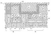
- FIG. 3illustrates a structure in accordance with exemplary embodiments of the present techniques for providing an interconnect at the storage node 46 for the transistor 36 , transistor 48 and capacitor 38 at the storage node 46 .
- the memory cell 30may be fabricated on a substrate by implementing a number of manufacturing processes, such as layering, doping, patterning and heat treatments.
- layeringgenerally refers to adding material to the surface of a substrate by a growth process such as oxidation, or through a deposition process, such as chemical vapor deposition (CVD) or a physical vapor deposition (PVD).
- CVDchemical vapor deposition
- PVDphysical vapor deposition
- Dopinggenerally refers to the process of implanting dopants into the substrate surface or overlying layers and may be used to increase the current carrying capacity of a region of the wafer or overlying layer of material.
- the doping processmay be implemented before a layer is formed, between layers, or even after the layer is formed.
- the doping the processmay be accomplished through an ion implantation process using boron or other similar dopants, or through a thermal diffusion process, for example.
- Patterninggenerally refers to a series of steps that result in the removal of selected portions of layers or underlying substrate material. After removal of the selected portions of the layers via a wet or dry etch process, a pattern is left in the structure. The removal of material allows the structure of the device to be formed by providing holes or windows between layers or by removing unwanted layers. Patterning sets the critical dimensions of the integrated circuit structures being fabricated. Those having ordinary skill in the art will appreciate the many manufacturing steps involved in fabricating the structure illustrated in FIG. 3 . Accordingly, the particular process flow that may be implemented to fabricate the structure illustrated in FIG. 3 may vary and is not described in detail, herein.
- FIG. 3is a cross-sectional view of the storage node 46 and surrounding structures in accordance with embodiments of the present invention.
- the structureis generally illustrated by the reference numeral 52 .
- the structure 52utilizes the lower metal cell plate of the capacitor 38 as the storage node 46 to couple the gate of the transistor 48 in the CAM portion 34 of the memory cell 30 to the source 44 of the transistor 36 in the DRAM portion 32 of the memory cell 30 .
- the structure 52allows for a compact array layout without disturbing the critical structures of the storage node 46 .
- the memory cell 30may be fabricated on a substrate 54 such as a p-type silicon substrate.
- the substrate 54includes doped/active regions formed by a suitable doping technique such as ion implantation. The doped regions form the drain 42 and source 44 of the access transistor 36 .
- a conductive post 56such as a polysilicon post, may be implemented.
- the post 56is further coupled to a conductive material 58 , such as tungsten (W), which may form the digit line of the memory array.
- a conductive post 60such as a polysilicon post may be implemented.
- the gate 40is fabricated to form the wordline of the memory array.
- the gate 40generally includes a gate oxide layer 62 disposed on the substrate 54 and configured to insulate the channel for the access transistor 36 .
- a conductive polysilicon layer 64is disposed on the gate oxide layer 62 and patterned in accordance with the dimensions of the underlying channel.
- one or more conductive layers 66such as tungsten and tungsten silicide, may be disposed and patterned over the polysilicon layer 64 .
- a cap 68may be disposed on the conductive layer 66 to project the underlying materials from damage during fabrication of the structure 52 .
- the cap 68may include one or more dielectric materials such as nitride or tetra ethyl oxysilane (TEOS).
- TEOStetra ethyl oxysilane
- spacers 70comprising one or more dielectric materials such as nitride, may be fabricated.
- the gate 47may be fabricated in conjunction with the gate 40 of the transistor 36 and may include the same materials. Accordingly, the gate 47 includes a gate oxide layer 72 , a polysilicon layer 74 , a conductive layer 76 , a dielectric cap 78 and dielectric spacers 80 . Because the formation of the source and drain of the transistor 48 are not pertinent to the present embodiments, these structures are not illustrated. However, one skilled in the art will be aware that these structures are formed along the gate 47 at a point further down the z-axis (i.e., into the page).
- a dielectric material 82is disposed within shallow trenches etched in the substrate 54 . Once the shallow trenches are etched in the substrate 54 , a dielectric material such as an oxide 82 may be disposed therein. As will be appreciated, the drain and source of the transistor 48 are formed behind the presently illustrated oxide regions 82 . Finally, to couple the gate 47 of the transistor 48 to the access node 46 , a conductive post 84 , such as a tungsten post, may be formed. As will be appreciated, during formation of the post opening, a punch process may be implemented to punch through the cap layer 78 to provide contact to the underlying conductive layer 76 .
- Each of the transistor 36 and transistor 48may be formed through a number of layering, patterning, doping and anneal processes, as previously described.
- a dielectric layer 86such as a phosphosilicate glass (PSG) layer is disposed to bury the transistors 36 and 48 .
- the posts 56 , 60 and 84are generally formed after deposition of the dielectric layer 86 .
- the contacts to the various nodes of the transistorsi.e., post 56 , post 60 and post 84
- the capacitor 38may be fabricated.
- a container type storage capacitor 38is implemented and the lower metal cell plate 88 of the capacitor 38 is couple directly to the conductive posts 60 and 64 .
- the lower cell plate 88 of the capacitor 38may comprise titanium nitride, for instance.
- the upper cell plate 90 of the capacitor 38may comprise a titanium nitride material.
- the upper and lower cell plates 90 and 88are separated by a dielectric layer such as an aluminum oxide (Al 2 O 3 ) 92 .
- a dielectric layer 94which may include one or more dielectric materials such as phosphosilicate glass (PSG).
- the present embodimentadvantageously increases the capacitive area by increasing the size of the lower cell plate 88 .
- contact resistancemay be increased while minimizing leakage potential.
- the formation of the posts 60 and 84may be performed at different steps in the fabrication, thereby reducing potential fabrication difficulties.
- a polysilicon material to form the posts 56 and 60 to contact the source and drain of the transistorleakage through the active regions of the drains 42 and source 44 in the silicon substrate 54 may be reduced.
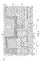
- FIG. 4a cut away top view of the lower cell plate 88 and underlying posts 60 and 84 is shown to illustrate the increased size of the lower cell plate 88 .
- the increased cell plateprovides and increased capacitive area.
- the surface area of the lower cell plate 88is generally greater than the surface area of the cell plate in conventional devices because the lower cell plate 88 may be extended over the transistors 36 and 48 such that the corresponding posts 60 and 84 may be coupled directly thereto.
- the lower cell plate 88may have an area of 100 nm by 300 nm.
- the lower cell plate 88is integrated as the interconnect between the capacitor 38 and the gate 47 to form the storage node 46 .
- the present embodimentsmerge the interconnect function with the storage function of the capacitor 38 .
- the posts 60 and 84may be advantageous to fabricate the posts 60 and 84 such that they are separated by a reduced distance D.
- the distance Dwill vary depending on the fabrication technology implemented. For instance, in a 100 nm process, the distance D may be on the order of approximately 50 nm. For a 50 nm process, the distance D may be on the order of approximately 20 nm. In another exemplary embodiment, it may be advantageous to increase the distance D. Because of the increased size of the lower cell plate 88 , the posts 60 an 84 the distance D can be increased.
Landscapes
- Engineering & Computer Science (AREA)
- Microelectronics & Electronic Packaging (AREA)
- Computer Hardware Design (AREA)
- Manufacturing & Machinery (AREA)
- Semiconductor Memories (AREA)
Abstract
Description
Claims (26)
Priority Applications (1)
| Application Number | Priority Date | Filing Date | Title |
|---|---|---|---|
| US10/750,737US6979849B2 (en) | 2003-12-31 | 2003-12-31 | Memory cell having improved interconnect |
Applications Claiming Priority (1)
| Application Number | Priority Date | Filing Date | Title |
|---|---|---|---|
| US10/750,737US6979849B2 (en) | 2003-12-31 | 2003-12-31 | Memory cell having improved interconnect |
Publications (2)
| Publication Number | Publication Date |
|---|---|
| US20050139884A1 US20050139884A1 (en) | 2005-06-30 |
| US6979849B2true US6979849B2 (en) | 2005-12-27 |
Family
ID=34701245
Family Applications (1)
| Application Number | Title | Priority Date | Filing Date |
|---|---|---|---|
| US10/750,737Expired - Fee RelatedUS6979849B2 (en) | 2003-12-31 | 2003-12-31 | Memory cell having improved interconnect |
Country Status (1)
| Country | Link |
|---|---|
| US (1) | US6979849B2 (en) |
Cited By (2)
| Publication number | Priority date | Publication date | Assignee | Title |
|---|---|---|---|---|
| US10163480B1 (en)* | 2017-07-27 | 2018-12-25 | Micron Technology, Inc. | Periphery fill and localized capacitance |
| US10475489B2 (en) | 2017-07-27 | 2019-11-12 | Micron Technology, Inc. | Variable filter capacitance |
Families Citing this family (7)
| Publication number | Priority date | Publication date | Assignee | Title |
|---|---|---|---|---|
| US7294879B2 (en)* | 2003-07-18 | 2007-11-13 | International Business Machines Corporation | Vertical MOSFET with dual work function materials |
| KR100701697B1 (en)* | 2005-06-29 | 2007-03-29 | 주식회사 하이닉스반도체 | Manufacturing method of CMOS device having dual polyside gate |
| US7729149B2 (en)* | 2007-05-01 | 2010-06-01 | Suvolta, Inc. | Content addressable memory cell including a junction field effect transistor |
| US7633784B2 (en)* | 2007-05-17 | 2009-12-15 | Dsm Solutions, Inc. | Junction field effect dynamic random access memory cell and content addressable memory cell |
| US8546876B2 (en) | 2008-03-20 | 2013-10-01 | Micron Technology, Inc. | Systems and devices including multi-transistor cells and methods of using, making, and operating the same |
| US7969776B2 (en)* | 2008-04-03 | 2011-06-28 | Micron Technology, Inc. | Data cells with drivers and methods of making and operating the same |
| JP5998458B2 (en) | 2011-11-15 | 2016-09-28 | セイコーエプソン株式会社 | Pixel circuit, electro-optical device, and electronic apparatus |
Citations (18)
| Publication number | Priority date | Publication date | Assignee | Title |
|---|---|---|---|---|
| US4903110A (en)* | 1987-06-15 | 1990-02-20 | Nec Corporation | Single plate capacitor having an electrode structure of high adhesion |
| US6011284A (en)* | 1996-12-26 | 2000-01-04 | Sony Corporation | Electronic material, its manufacturing method, dielectric capacitor, nonvolatile memory and semiconductor device |
| US6207987B1 (en)* | 1998-06-03 | 2001-03-27 | Mitsubishi Denki Kabushiki Kaisha | Semiconductor device having smooth surface for suppressing layer displacement |
| US20010022369A1 (en)* | 1997-12-19 | 2001-09-20 | Takuya Fukuda | Semiconductor integrated circuit device |
| US20010045589A1 (en)* | 2000-05-26 | 2001-11-29 | Fujitsu Limited | Semiconductor device with memory and logic cells |
| US20020024073A1 (en)* | 2000-03-13 | 2002-02-28 | Yasuhiro Shimada | Semiconductor device and method for fabricating the same |
| US20020028562A1 (en)* | 2000-08-31 | 2002-03-07 | Hynix Semiconductor, Inc. | Method for fabricating a lower plate for a capacitor of semiconductor device |
| US20020089059A1 (en)* | 2001-01-10 | 2002-07-11 | Shinichi Imai | Semiconductor device and method for manufacturing the same |
| US20020135005A1 (en)* | 1996-04-26 | 2002-09-26 | Micron Technology, Inc. | Method of making EEPROM transistor for a DRAM |
| US6607980B2 (en)* | 2001-02-12 | 2003-08-19 | Symetrix Corporation | Rapid-temperature pulsing anneal method at low temperature for fabricating layered superlattice materials and making electronic devices including same |
| US6730950B1 (en)* | 2003-01-07 | 2004-05-04 | Texas Instruments Incorporated | Local interconnect using the electrode of a ferroelectric |
| US6743643B2 (en)* | 2001-11-29 | 2004-06-01 | Symetrix Corporation | Stacked memory cell having diffusion barriers |
| US20040129963A1 (en)* | 2003-01-07 | 2004-07-08 | Renesas Technology Corp. | Semiconductor device and manufacturing method thereof |
| US20040150019A1 (en)* | 2003-02-04 | 2004-08-05 | Renesas Technology Corp. | Semiconductor memory device |
| US6815223B2 (en)* | 2002-11-22 | 2004-11-09 | Symetrix Corporation | Low thermal budget fabrication of ferroelectric memory using RTP |
| US6844583B2 (en)* | 2001-06-26 | 2005-01-18 | Samsung Electronics Co., Ltd. | Ferroelectric memory devices having expanded plate lines |
| US6858443B2 (en)* | 2002-02-20 | 2005-02-22 | Samsung Electronics Co., Ltd. | Methods of forming ferroelectric capacitors on protruding portions of conductive plugs having a smaller cross-sectional size than base portions thereof |
| US6864527B2 (en)* | 1998-02-26 | 2005-03-08 | Micron Technology, Inc. | Capacitor having tantalum oxynitride film and method for making same |
- 2003
- 2003-12-31USUS10/750,737patent/US6979849B2/ennot_activeExpired - Fee Related
Patent Citations (18)
| Publication number | Priority date | Publication date | Assignee | Title |
|---|---|---|---|---|
| US4903110A (en)* | 1987-06-15 | 1990-02-20 | Nec Corporation | Single plate capacitor having an electrode structure of high adhesion |
| US20020135005A1 (en)* | 1996-04-26 | 2002-09-26 | Micron Technology, Inc. | Method of making EEPROM transistor for a DRAM |
| US6011284A (en)* | 1996-12-26 | 2000-01-04 | Sony Corporation | Electronic material, its manufacturing method, dielectric capacitor, nonvolatile memory and semiconductor device |
| US20010022369A1 (en)* | 1997-12-19 | 2001-09-20 | Takuya Fukuda | Semiconductor integrated circuit device |
| US6864527B2 (en)* | 1998-02-26 | 2005-03-08 | Micron Technology, Inc. | Capacitor having tantalum oxynitride film and method for making same |
| US6207987B1 (en)* | 1998-06-03 | 2001-03-27 | Mitsubishi Denki Kabushiki Kaisha | Semiconductor device having smooth surface for suppressing layer displacement |
| US20020024073A1 (en)* | 2000-03-13 | 2002-02-28 | Yasuhiro Shimada | Semiconductor device and method for fabricating the same |
| US20010045589A1 (en)* | 2000-05-26 | 2001-11-29 | Fujitsu Limited | Semiconductor device with memory and logic cells |
| US20020028562A1 (en)* | 2000-08-31 | 2002-03-07 | Hynix Semiconductor, Inc. | Method for fabricating a lower plate for a capacitor of semiconductor device |
| US20020089059A1 (en)* | 2001-01-10 | 2002-07-11 | Shinichi Imai | Semiconductor device and method for manufacturing the same |
| US6607980B2 (en)* | 2001-02-12 | 2003-08-19 | Symetrix Corporation | Rapid-temperature pulsing anneal method at low temperature for fabricating layered superlattice materials and making electronic devices including same |
| US6844583B2 (en)* | 2001-06-26 | 2005-01-18 | Samsung Electronics Co., Ltd. | Ferroelectric memory devices having expanded plate lines |
| US6743643B2 (en)* | 2001-11-29 | 2004-06-01 | Symetrix Corporation | Stacked memory cell having diffusion barriers |
| US6858443B2 (en)* | 2002-02-20 | 2005-02-22 | Samsung Electronics Co., Ltd. | Methods of forming ferroelectric capacitors on protruding portions of conductive plugs having a smaller cross-sectional size than base portions thereof |
| US6815223B2 (en)* | 2002-11-22 | 2004-11-09 | Symetrix Corporation | Low thermal budget fabrication of ferroelectric memory using RTP |
| US6730950B1 (en)* | 2003-01-07 | 2004-05-04 | Texas Instruments Incorporated | Local interconnect using the electrode of a ferroelectric |
| US20040129963A1 (en)* | 2003-01-07 | 2004-07-08 | Renesas Technology Corp. | Semiconductor device and manufacturing method thereof |
| US20040150019A1 (en)* | 2003-02-04 | 2004-08-05 | Renesas Technology Corp. | Semiconductor memory device |
Cited By (5)
| Publication number | Priority date | Publication date | Assignee | Title |
|---|---|---|---|---|
| US10163480B1 (en)* | 2017-07-27 | 2018-12-25 | Micron Technology, Inc. | Periphery fill and localized capacitance |
| US10475489B2 (en) | 2017-07-27 | 2019-11-12 | Micron Technology, Inc. | Variable filter capacitance |
| US10559339B2 (en) | 2017-07-27 | 2020-02-11 | Micron Technology, Inc. | Periphery fill and localized capacitance |
| US10878861B2 (en) | 2017-07-27 | 2020-12-29 | Micron Technology, Inc. | Variable filter capacitance |
| US10950286B2 (en) | 2017-07-27 | 2021-03-16 | Micron Technology, Inc. | Periphery fill and localized capacitance |
Also Published As
| Publication number | Publication date |
|---|---|
| US20050139884A1 (en) | 2005-06-30 |
Similar Documents
| Publication | Publication Date | Title |
|---|---|---|
| US5547893A (en) | method for fabricating an embedded vertical bipolar transistor and a memory cell | |
| US9064728B2 (en) | Method and apparatus for fabricating a memory device with a dielectric etch stop layer | |
| US5867420A (en) | Reducing oxidation stress in the fabrication of devices | |
| US6657265B2 (en) | Semiconductor device and its manufacturing method | |
| US20150357233A1 (en) | Method and apparatus for fabricating a memory device with a dielectric etch stop layer | |
| US6251722B1 (en) | Method of fabricating a trench capacitor | |
| US6979849B2 (en) | Memory cell having improved interconnect | |
| US8012836B2 (en) | Semiconductor devices and methods for fabricating the same | |
| US6329232B1 (en) | Method of manufacturing a semiconductor device | |
| JP2003158195A (en) | Method for manufacturing semiconductor integrated circuit device | |
| US7230312B2 (en) | Transistor having vertical junction edge and method of manufacturing the same | |
| US8445372B2 (en) | Selective silicide formation using resist etch back | |
| US5068698A (en) | MOS semiconductor device having high-capacity stacked capacitor | |
| US6867131B2 (en) | Apparatus and method of increasing sram cell capacitance with metal fill | |
| US6146949A (en) | Method of manufacturing mask ROM devices with self-aligned coding implant | |
| US5744388A (en) | Process of making a storage capacitor for dram memory cell | |
| CN113629009B (en) | Method for manufacturing semiconductor cobalt silicide film layer, semiconductor device and memory | |
| US6797557B2 (en) | Methods and systems for forming embedded DRAM for an MIM capacitor | |
| US6734089B1 (en) | Techniques for improving wordline fabrication of a memory device | |
| US6200861B1 (en) | Method of fabricating high density multiple states mask ROM cells | |
| CN100356551C (en) | Dynamic random access memory unit and manufacturing method thereof | |
| EP0813241A1 (en) | Storage capacitor for DRAM memory cell and the process of fabricating the same | |
| US6204113B1 (en) | Method of forming data storage capacitors in dynamic random access memory cells | |
| US20050148145A1 (en) | Semiconductor memory cell with buried dopant bit lines and salicided polysilicon word lines isolated by an array of blocks | |
| KR20020075219A (en) | Semiconductor memory device for reducing parasitic capacitance and fabrication method thereof |
Legal Events
| Date | Code | Title | Description |
|---|---|---|---|
| AS | Assignment | Owner name:MICRON TECHNOLOGY, INC., IDAHO Free format text:ASSIGNMENT OF ASSIGNORS INTEREST;ASSIGNOR:LANE, RICHARD;REEL/FRAME:014874/0413 Effective date:20031230 | |
| FEPP | Fee payment procedure | Free format text:PAYOR NUMBER ASSIGNED (ORIGINAL EVENT CODE: ASPN); ENTITY STATUS OF PATENT OWNER: LARGE ENTITY | |
| FPAY | Fee payment | Year of fee payment:4 | |
| FPAY | Fee payment | Year of fee payment:8 | |
| AS | Assignment | Owner name:U.S. BANK NATIONAL ASSOCIATION, AS COLLATERAL AGENT, CALIFORNIA Free format text:SECURITY INTEREST;ASSIGNOR:MICRON TECHNOLOGY, INC.;REEL/FRAME:038669/0001 Effective date:20160426 Owner name:U.S. BANK NATIONAL ASSOCIATION, AS COLLATERAL AGEN Free format text:SECURITY INTEREST;ASSIGNOR:MICRON TECHNOLOGY, INC.;REEL/FRAME:038669/0001 Effective date:20160426 | |
| AS | Assignment | Owner name:MORGAN STANLEY SENIOR FUNDING, INC., AS COLLATERAL AGENT, MARYLAND Free format text:PATENT SECURITY AGREEMENT;ASSIGNOR:MICRON TECHNOLOGY, INC.;REEL/FRAME:038954/0001 Effective date:20160426 Owner name:MORGAN STANLEY SENIOR FUNDING, INC., AS COLLATERAL Free format text:PATENT SECURITY AGREEMENT;ASSIGNOR:MICRON TECHNOLOGY, INC.;REEL/FRAME:038954/0001 Effective date:20160426 | |
| AS | Assignment | Owner name:U.S. BANK NATIONAL ASSOCIATION, AS COLLATERAL AGENT, CALIFORNIA Free format text:CORRECTIVE ASSIGNMENT TO CORRECT THE REPLACE ERRONEOUSLY FILED PATENT #7358718 WITH THE CORRECT PATENT #7358178 PREVIOUSLY RECORDED ON REEL 038669 FRAME 0001. ASSIGNOR(S) HEREBY CONFIRMS THE SECURITY INTEREST;ASSIGNOR:MICRON TECHNOLOGY, INC.;REEL/FRAME:043079/0001 Effective date:20160426 Owner name:U.S. BANK NATIONAL ASSOCIATION, AS COLLATERAL AGEN Free format text:CORRECTIVE ASSIGNMENT TO CORRECT THE REPLACE ERRONEOUSLY FILED PATENT #7358718 WITH THE CORRECT PATENT #7358178 PREVIOUSLY RECORDED ON REEL 038669 FRAME 0001. ASSIGNOR(S) HEREBY CONFIRMS THE SECURITY INTEREST;ASSIGNOR:MICRON TECHNOLOGY, INC.;REEL/FRAME:043079/0001 Effective date:20160426 | |
| REMI | Maintenance fee reminder mailed | ||
| LAPS | Lapse for failure to pay maintenance fees | Free format text:PATENT EXPIRED FOR FAILURE TO PAY MAINTENANCE FEES (ORIGINAL EVENT CODE: EXP.) | |
| STCH | Information on status: patent discontinuation | Free format text:PATENT EXPIRED DUE TO NONPAYMENT OF MAINTENANCE FEES UNDER 37 CFR 1.362 | |
| FP | Lapsed due to failure to pay maintenance fee | Effective date:20171227 | |
| AS | Assignment | Owner name:MICRON TECHNOLOGY, INC., IDAHO Free format text:RELEASE BY SECURED PARTY;ASSIGNOR:U.S. BANK NATIONAL ASSOCIATION, AS COLLATERAL AGENT;REEL/FRAME:047243/0001 Effective date:20180629 | |
| AS | Assignment | Owner name:MICRON TECHNOLOGY, INC., IDAHO Free format text:RELEASE BY SECURED PARTY;ASSIGNOR:MORGAN STANLEY SENIOR FUNDING, INC., AS COLLATERAL AGENT;REEL/FRAME:050937/0001 Effective date:20190731 |