US6977824B1 - Control circuit for controlling output current at the primary side of a power converter - Google Patents
Control circuit for controlling output current at the primary side of a power converterDownload PDFInfo
- Publication number
- US6977824B1 US6977824B1US10/914,802US91480204AUS6977824B1US 6977824 B1US6977824 B1US 6977824B1US 91480204 AUS91480204 AUS 91480204AUS 6977824 B1US6977824 B1US 6977824B1
- Authority
- US
- United States
- Prior art keywords
- signal
- capacitor
- current
- osc
- zcd
- Prior art date
- Legal status (The legal status is an assumption and is not a legal conclusion. Google has not performed a legal analysis and makes no representation as to the accuracy of the status listed.)
- Expired - Lifetime
Links
- 230000010355oscillationEffects0.000claimsabstractdescription26
- 230000002596correlated effectEffects0.000claimsabstractdescription18
- 230000001276controlling effectEffects0.000claimsabstractdescription9
- 230000001105regulatory effectEffects0.000claimsabstractdescription9
- 239000003990capacitorSubstances0.000claimsdescription127
- 238000005070samplingMethods0.000claimsdescription22
- 238000004804windingMethods0.000claimsdescription18
- 238000007599dischargingMethods0.000claimsdescription12
- 238000001514detection methodMethods0.000claimsdescription8
- 230000003111delayed effectEffects0.000claimsdescription6
- 230000000630rising effectEffects0.000claimsdescription6
- 238000010586diagramMethods0.000description10
- 239000008186active pharmaceutical agentSubstances0.000description4
- 101100219315Arabidopsis thaliana CYP83A1 geneProteins0.000description3
- 101100269674Mus musculus Alyref2 geneProteins0.000description3
- 101100140580Saccharomyces cerevisiae (strain ATCC 204508 / S288c) REF2 geneProteins0.000description3
- 230000004048modificationEffects0.000description2
- 238000012986modificationMethods0.000description2
- 230000001960triggered effectEffects0.000description2
- 230000033228biological regulationEffects0.000description1
- 238000002955isolationMethods0.000description1
Images


Classifications
- H—ELECTRICITY
- H02—GENERATION; CONVERSION OR DISTRIBUTION OF ELECTRIC POWER
- H02M—APPARATUS FOR CONVERSION BETWEEN AC AND AC, BETWEEN AC AND DC, OR BETWEEN DC AND DC, AND FOR USE WITH MAINS OR SIMILAR POWER SUPPLY SYSTEMS; CONVERSION OF DC OR AC INPUT POWER INTO SURGE OUTPUT POWER; CONTROL OR REGULATION THEREOF
- H02M3/00—Conversion of DC power input into DC power output
- H02M3/22—Conversion of DC power input into DC power output with intermediate conversion into AC
- H02M3/24—Conversion of DC power input into DC power output with intermediate conversion into AC by static converters
- H02M3/28—Conversion of DC power input into DC power output with intermediate conversion into AC by static converters using discharge tubes with control electrode or semiconductor devices with control electrode to produce the intermediate AC
- H02M3/325—Conversion of DC power input into DC power output with intermediate conversion into AC by static converters using discharge tubes with control electrode or semiconductor devices with control electrode to produce the intermediate AC using devices of a triode or a transistor type requiring continuous application of a control signal
- H02M3/335—Conversion of DC power input into DC power output with intermediate conversion into AC by static converters using discharge tubes with control electrode or semiconductor devices with control electrode to produce the intermediate AC using devices of a triode or a transistor type requiring continuous application of a control signal using semiconductor devices only
- H02M3/33507—Conversion of DC power input into DC power output with intermediate conversion into AC by static converters using discharge tubes with control electrode or semiconductor devices with control electrode to produce the intermediate AC using devices of a triode or a transistor type requiring continuous application of a control signal using semiconductor devices only with automatic control of the output voltage or current, e.g. flyback converters
Definitions
- the present inventionrelates to a power converter, and more particularly, to the control circuit of the power converter.
- the present inventionprovides a control circuit for controlling an output current at a primary side of a power converter.
- the control circuitcomprises a switching control circuit for generating a switching signal for switching a transformer and regulating an output of the power converter.
- the switching control circuitincludes an operational amplifier and a reference voltage developing an error amplifier for output current control, a comparator associated with a PWM circuit controlling the pulse width of the switching signal in response to the output of the error amplifier.
- the control circuitfurther comprises an oscillator generates an oscillation signal for determining the switching frequency of the switching signal.
- a waveform detectorgenerates a current-waveform signal by sampling a primary side switching current signal.
- a discharge-time detectorcoupled to the transformer detects a discharge-time of the secondary side switching current.
- An integratorproduces an integrated signal by integrating an average current signal with the discharge-time. The integrated signal is coupled to the input of the error amplifier, therefore the output current of the power converter is regulated.
- the average current signalis produced in response to the current-waveform signal, and the time constant of the integrator is correlated with a switching period of the switching signal. Therefore the integrated signal is proportional to the output current of the power converter.
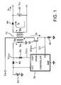
- FIG. 1illustrates a schematic diagram of a power converter according to one embodiment of the present invention.
- FIG. 2illustrates the key waveforms of the conventional power converter operating in discontinuous conduction mode according to one embodiment of the present invention.
- FIG. 3illustrates the key waveforms of the conventional power converter operating in continuous conduction mode according to one embodiment of the present invention.
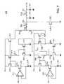
- FIG. 4illustrates a control circuit for output current control according to one preferred embodiment of the present invention.
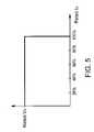
- FIG. 5shows the output voltage curve versus the variation of the output current according to one embodiment of the present invention.
- FIG. 6illustrates a schematic circuit diagram of a waveform detector according to one embodiment of the present invention.
- FIG. 7illustrates a schematic circuit diagram of an integrator according to one embodiment of the present invention.
- FIG. 8illustrates a schematic circuit diagram of an oscillator according to one embodiment of the present invention.
- FIG. 9illustrates a schematic diagram of a discharge-time detector according to one embodiment of the present invention.
- the power convertercomprises a transformer 10 having an auxiliary winding N A , a primary winding N P , and a secondary winding N S .
- a control circuit 70In order to regulate the output voltage V O and/or the output current I O of the power converter, a control circuit 70 generates a switching signal V PWM to switch the transformer 10 by switching a transistor 20 .
- FIG. 2it illustrates various signal waveforms of the power converter in FIG. 1 operating in discontinuous conduction mode. A primary side switching current I P is generated as the switching signal V PWM becomes high.
- V AUXT NA T NS ⁇ ( V O + V F ) ( 3 )
- T NA and T NSare respectively the winding turns of the auxiliary winding N A and the secondary winding N S of the transformer 10 .
- the discharging time T DSD in equation (2)can be measured from the falling edge of the switching signal V PWM to the falling point of the reflected voltage V AUX .
- the discontinuous conduction mode of the power converterfeatures that the energy of the transformer 10 is fully released before the next switching cycle starts.
- the continuous conduction modefeatures that the energy of the transformer 10 is not fully released as the next switching cycle starts.
- FIG. 3shows the waveforms of the power converter operating in continuous conduction mode. A peak value I P(PEAK) of the primary side switching current I P in continuous conduction mode is given by,
- I P(PEAK)I PA+ I PB (4)
- I PAV IN L P ⁇ T ON ( 5 )
- I PBrepresents the energy stored in the transformer 10 .
- the secondary side switching current I Sis determined by the primary side switching current I P and the winding turns of the transformer 10 .
- the control circuit 70comprises a supply terminal VCC, a voltage-detection terminal VDET, a ground terminal GND, a current-sense terminal VS, and an output terminal VPWM.
- the output terminal VPWMoutputs the switching signal V PWM .
- the voltage-detection terminal VDETis coupled to the auxiliary winding N A via a resistor 50 for detecting the reflected voltage V AUX .
- the reflected voltage V AUXfurther charges a capacitor 65 via a rectifier 60 for powering the control circuit 70 .
- a current-sense resistor 30is coupled from a source of the transistor 20 to a ground reference level for converting the primary side switching current I P to a primary side switching current signal V IP .
- the current-sense terminal VSis coupled to a current-sense device such as a current-sense resistor 30 .
- FIG. 4it illustrates a schematic diagram of the control circuit 70 for output current control according to one embodiment of the present invention.
- a waveform detector 300generates current-waveform signals V A and V B by sampling the primary side switching current signal V IP .
- a discharge-time detector 100detects the discharging time T DSD /T DSC of the secondary side switching current I S via the auxiliary winding N A of the transformer 10 .
- An oscillator 200generates an oscillation signal PLS to determine the switching frequency of the switching signal V PWM .
- An integrator 500is used to generate an integrated signal V X by integrating an average current signal I AVG with the discharging time T DSD /T DSC .
- the average current signal I AVGis produced in response to current-waveform signals V A and V B . Both discontinuous conduction mode and continuous conduction mode are considered.
- a time constant of the integrator 500is correlated with a switching period T of the switching signal V PWM .
- the integrated signal V Xis therefore proportional to the output current I O of the power converter.
- a switching control circuitincludes an operational amplifier 71 and a reference voltage V REF1 developing an error amplifier for output current control, a comparator 75 associated with a PWM circuit 400 controlling the pulse width of the switching signal V PWM in response to an output of the error amplifier.
- the error amplifieramplifies the integrated signal V X and provides a loop gain for output current control.
- a current control loopis formed from detecting the primary side switching current I P to modulating the pulse width of the switching signal V PWM .
- the current control loopcontrols the magnitude of the primary side switching current I P in response to the reference voltage V REF1 .
- the secondary side switching current I Sis a ratio of the primary side switching current I P as shown in equation (6). Referring to the waveform in FIG. 2 and/or FIG.
- the output current I O of the power converteris the average of the secondary side switching current I S .
- the output current I O of the power converteris therefore regulated.
- the primary side switching current I Pis converted to the primary side switching current signal V IP by the current-sense resistor 30 .
- the waveform detector 300detects the primary side switching current signal V IP and generates current-waveform signals V A and V B .
- V XT T I ⁇ T NS T NP ⁇ R S ⁇ I O ( 11 )
- the integrated signal V Xis proportional to the output current I O of the power converter.
- the integrated signal V Xincreases whenever the output current I O increases.
- the maximum value of the integrated signal V Xis limited to the value of the reference voltage V REF1 through the regulation of the current control loop.
- I O(MAX)T NP T NS ⁇ G A ⁇ G SW ⁇ V R1 1 + ( G A ⁇ G SW ⁇ R S K ) ( 12 )
- Kis a constant equal to T 1 /T
- V R1is the value of the reference voltage V REF1
- G Ais the gain of the error amplifier
- G SWis the gain of the switching circuit.
- I O(MAX)K ⁇ T NP T NS ⁇ V R1 R S ( 13 )
- the maximum output current I O(MAX) of the power converteris thus regulated as a constant current in accordance with the reference voltage V REF1 .
- FIG. 5shows the output voltage V O curve versus the variation of the output current I O .
- the PWM circuit 400outputs the switching signal V PWM for switching the power converter.
- the PWM circuit 400according to one embodiment of the present invention comprises a D flip-flop 95 , an inverter 93 , an AND gate 91 and an AND gate 92 .
- a D input of the D flip-flop 95is supplied with a supply voltage V CC .
- the oscillation signal PLSsets the D flip-flop 95 through the inverter 93 .
- An output of the D flip-flop 95is coupled to a first input of the AND gate 92 .
- a second input of the AND gate 92is coupled to an output of the inverter 93 .
- An output of the AND gate 92is also an output of the PWM circuit 400 , which generates the switching signal V PWM .
- the D flip-flop 95is reset by an output of the AND gate 91 .
- a first input of the AND gate 91is supplied with a voltage-loop signal S V .
- the voltage-loop signal S Vis generated by a voltage control loop, in which the voltage control loop is utilized to regulate the output voltage V O of the power converter.
- a current-loop signal S I generated from an output of the comparator 75is supplied to a second input of the AND gate 91 for achieving output current control.
- a positive input of the comparator 75is coupled to an output of the operational amplifier 71 .
- a negative input of the comparator 75is supplied with a ramp signal RMP that is provided by the oscillator 200 .
- the voltage-loop signal S V and the current-loop signal S Ican reset the D flip-flop 95 for shorten the pulse width of the switching signal V PWM so as to regulate the output voltage V O and the output current I O .
- FIG. 6it illustrates a schematic circuit diagram of the detector 300 according to one embodiment of the present invention.
- a comparator 310has a positive input coupled to the current-sense terminal VS. The value of the primary side switching current signal V IP is proportional to the value of the primary side switching current I P .
- a capacitor 321is used to hold the peak value of the primary side switching current signal V IP .
- a negative input of the comparator 310is coupled to the capacitor 321 .
- a constant current source 305is applied to charge the capacitor 321 .
- a switch 311is coupled between the constant current source 305 and the capacitor 321 . The switch 311 is turned on/off by an output of the comparator 310 .
- a peak voltage signal V SPis thus generated across the capacitor 321 .
- the peak voltage signal V SPis proportional to the sum current of I PA and I PB shown in FIG. 3 .
- a transistor 308is coupled in parallel with the capacitor 321 to discharge the capacitor 321 .
- a switch 312is used for periodically sampling the peak voltage signal V SP from the capacitor 321 to a capacitor 322 . Then the current-waveform signal V A is obtained across the capacitor 322 .
- a switch 314is coupled between the current-sense terminal VS and a capacitor 324 .
- the capacitor 324is used to hold the initial value of the primary side switching current signal V IP .
- An initial voltage signal V SIis therefore generated across the capacitor 324 .
- the initial voltage signal V SIis proportional to the value of the current I PB shown in FIG. 3 .
- a transistor 309is coupled in parallel with the capacitor 324 to discharge the capacitor 324 .
- a switch 315serves to periodically sample the initial voltage signal V SI from the capacitor 324 to a capacitor 325 . Then the current-waveform signal V B is generated across the capacitor 325 .
- An inverter 351 , a current source 352 , a transistor 353 , a capacitor 354 , and an AND gate 355form a first time-delay circuit.
- An inverter 361 , a current source 362 , a transistor 363 , a capacitor 364 , an AND gate 365 and an inverter 366form a first one-shot signal generator to output a store signal STR.
- the store signal STRis a one-shot signal.
- the switching signal V PWMis supplied to an input of the first time-delay circuit.
- a current I 352 of the current source 352 and the capacitance of the capacitor 354determine a delay time of the first time-delay circuit.
- An output of the first time-delay circuitis coupled to an input of the first one-shot signal generator.
- a current I 362 of the current source 362 and the capacitance of the capacitor 364determine the pulse width of the store signal STR.
- the store signal STRcontrols the switch 314 to sample the initial value of the primary side switching current signal V IP . Therefore the store signal STR is generated in response to the rising edge of a delayed switching signal.
- the delayed switching signalis generated in response to a rising edge of the switching signal V PWM after the delay time. The delay time serves to avoid sampling from the interference of the switching spike.
- FIG. 7it illustrates a schematic circuit diagram of an integrator 500 according to one embodiment of the present invention.
- An operational amplifier 510 , a resistor 511 and a transistor 512construct a first V-to-I converter to generate a first programmable current I 512 in response to the voltage of the current-waveform signal V B .
- Transistors 514 , 515 and 519form a first current mirror for producing a current I 515 and a current I 519 by mirroring the first programmable current I 512 .
- Transistors 516 and 517form a second current mirror for generating a current I 517 by mirroring the current I 515 .
- An operational amplifier 530 , a resistor 531 and a transistor 532form a second V-to-I converter for generating a second programmable current I 532 in response to the voltage of the current-waveform signal V A .
- Transistors 534 and 535form a third current mirror for producing a current I 535 by mirroring the second programmable current I 532 .
- Transistors 536 and 537develop a fourth current mirror for producing a current I 537 in response to the current I 535 and the current I 517 .
- the resistor 511 , the resistor 531 and the capacitor 570determine the time constant of the integrator 500 , in which the resistor 531 is correlated to the resistor 511 .
- a switch 550is coupled between the drain of the transistor 519 and a capacitor 570 .
- the switch 550is turned on only during the period of the discharge time T DS of secondary side switching current I S .
- a transistor 560is coupled in parallel with the capacitor 570 to discharge the capacitor 570 .
- a switch 551serves to periodically sample the voltage across the capacitor 570 to an output capacitor 571 .
- the integrated signal V Xis therefore generated across the output capacitor 571 .
- V X1 R 511 ⁇ ⁇ C 570 ⁇ ( V B + V A - V B 2 ) ⁇ T DS ( 16 )
- FIG. 8it illustrates a schematic diagram of the oscillator 200 according to one embodiment of the present invention.
- An operational amplifier 201 , a resistor 210 and a transistor 250form a third V-to-I converter.
- the third V-to-I convertergenerates a reference current I 250 in response to a reference voltage V REF2 .
- a plurality of transistors, such as 251 , 252 , 253 , 254 , 255form current mirrors for generating an oscillator charge current I 253 and an oscillator discharge current I 255 in response to the reference current I 250 .
- a drain of the transistor 253generates the oscillator charge current I 253 .
- a drain of the transistor 255generates the oscillator discharge current I 255 .
- a switch 230is coupled between the drain of the transistor 253 and a capacitor 215 .
- a switch 231is coupled between the drain of the transistor 255 and the capacitor 215 .
- the ramp signal RMPis obtained across the capacitor 215 .
- a comparator 205has a positive input connected to the capacitor 215 .
- the comparator 205outputs a oscillation signal PLS.
- the oscillation signal PLSdetermines the switching frequency and turns on/off the switches 312 , 315 and 551 .
- a first terminal of a switch 232is supplied with a high-threshold voltage V H .
- a first terminal of a switch 233is supplied with a low-threshold voltage V L .
- a second terminal of the switch 232 and a second terminal of the switch 233are both coupled to a negative input of the comparator 205 .
- An input of an inverter 260is coupled to an output of the comparator 205 for generating an inverse oscillation signal /PLS.
- the oscillation signal PLSturns on/off the switch 231 and the switch 233 .
- the inverse oscillation signal /PLSturns on/off the switch 230 and the switch 232 .
- Inverters 261 , 262 , 263 and 264are coupled in series.
- An input of the inverter 261is supplied with the oscillation signal PLS.
- An AND gate 270generates a clear signal CLR.
- a first input of the AND gate 270is coupled to an output of the inverter 264 .
- a second input of the AND gate 270is coupled to an output of the inverter 261 .
- the clear signal CLRturns on/off the transistors 308 , 309 and 560 .
- the resistance R 210 of the resistor 210 and the capacitance of the capacitor 215determine the switching period T of the switching signal V PWM .
- TC 215 ⁇ V OSC V REF2 /
- FIG. 9it illustrates a schematic diagram of the discharge-time detector 100 according to one embodiment of the present invention.
- An inverter 150 , a transistor 122 , a constant current source 120 , a capacitor 121 and an AND gate 155form a second time-delay circuit.
- An input of the second time-delay circuitis supplied with the switching signal V PWM .
- the second time-delay circuitprovides a propagation delay for the falling edge of the switching signal V PWM .
- a current I 120 of the constant current source 120 and the capacitance of the capacitor 121determine the timing of the propagation delay.
- An inverter 151 , an inverter 152 , a transistor 125 , a constant current source 123 , a capacitor 124 and an AND gate 156form a second one-shot signal generator for generating a voltage-sample signal SMP.
- An input of the second one-shot signal generatoris coupled to an output of the second time-delay circuit, which is also an output of the AND gate 155 .
- a current I 123 of the constant current source 123 and the capacitance of the capacitor 124determine the pulse width of the voltage-sample signal SMP.
- An operational amplifier 101performs as a buffer amplifier. A negative input and an output of the operational amplifier 101 are coupled together. A positive input of the operational amplifier 101 , which is also an input of the buffer amplifier, is coupled to the voltage-detection terminal VDET. The voltage-detection terminal VDET is coupled to the auxiliary winding N A of the transformer 10 via the resistor 50 for detecting the reflected voltage V AUX .
- a switch 109is coupled between an output of the buffer amplifier and a capacitor 112 . The switch 109 is turned on/off by the voltage-sample signal SMP. Therefore, the reflected voltage V AUX is sampled as a voltage V DET . The voltage V DET will be held across the capacitor 112 .
- a comparator 105is utilized to detect the decrease of the reflected voltage V AUX .
- a positive input of the comparator 105is coupled to the capacitor 112 .
- a reference voltage 106is coupled between a negative input of the comparator 105 and the output of the buffer amplifier to provide a threshold for detecting the decrease of the reflected voltage V AUX . Therefore, the comparator 105 outputs a logic-high signal as the decrement of the reflected voltage V AUX is beyond the voltage of the reference voltage 106 .
- An input of an inverter 115is supplied with the switching signal V PWM .
- An input of an inverter 116is supplied with the voltage-sample signal SMP.
- An AND gate 119has a first input connected to an output of the comparator 105 .
- a SR flip-flop 117 and a SR flip-flop 118have a rising-edge triggered set-input and a high-level triggered reset-input respectively.
- the set-input of the SR flip-flop 118is coupled to an output of the inverter 116 .
- the reset-input of the SR flip-flop 118is supplied with the switching signal V PWM .
- An output of the SR flip-flop 118is coupled to a second input of the AND gate 119 .
- An output of the SR flip-flop 117is coupled to a first input of an AND gate 114 .
- a second input of the AND gate 114is coupled to the output of the inverter 115 .
- An output of the AND gate 114serves to generate a discharge-time signal S DS .
- the set-input of the SR flip-flop 117is also coupled to the output of the inverter 115 .
- the reset-input of the SR flip-flop 117is coupled to an output of the AND gate 119 .
- the discharge-time signal S DSturns on/off the switch 550 .
- the pulse width of the discharge-time signal S DSis correlated to the discharge-time T DS of the secondary side switching current I S .
- the integrated signal V Xis correlated to the secondary side switching current I S and the output current I O of the power converter.
- the resistance R 511 of the resistor 511is correlated to the resistance R 210 of the resistor 210 .
- the capacitance C 570 of the capacitor 570is correlated to the capacitance C 215 of the capacitor 215 . Therefore, the integrated signal V X is proportional to the output current I O of the power converter.
Landscapes
- Engineering & Computer Science (AREA)
- Power Engineering (AREA)
- Dc-Dc Converters (AREA)
Abstract
Description
where VINis an input voltage applied to the
where VOis the output voltage of the power converter, VFis the forward voltage dropped across the
where TNAand TNSare respectively the winding turns of the auxiliary winding NAand the secondary winding NSof the
IP(PEAK)=IPA+IPB (4)
where TNPis the winding turns of the primary winding NPof the
where TDSrepresents TDSDin discontinuous conduction mode or TDSCin continuous conduction mode. The output current IOof the power converter is therefore regulated.
where
where the TIis the time constant of the
where K is a constant equal to T1/T, VR1is the value of the reference voltage VREF1, GAis the gain of the error amplifier, and GSWis the gain of the switching circuit.
I537=I535−I517
- in which I537=I535−I517. The geometric size of the
transistor 536 is twice the size of thetransistor 537. Therefore the current I537is the current I536divided by 2.Transistors transistor 519 and thetransistor 539 are coupled together for generating the average current signal IAVGby summing the current I159and the current I539. The average current signal IAVGcan be expressed by,
- in which I537=I535−I517. The geometric size of the
where VOSC=VH−VLand C215is the capacitance of the
where m is a constant, which can be determined by,
Claims (15)
Priority Applications (1)
| Application Number | Priority Date | Filing Date | Title |
|---|---|---|---|
| US10/914,802US6977824B1 (en) | 2004-08-09 | 2004-08-09 | Control circuit for controlling output current at the primary side of a power converter |
Applications Claiming Priority (1)
| Application Number | Priority Date | Filing Date | Title |
|---|---|---|---|
| US10/914,802US6977824B1 (en) | 2004-08-09 | 2004-08-09 | Control circuit for controlling output current at the primary side of a power converter |
Publications (1)
| Publication Number | Publication Date |
|---|---|
| US6977824B1true US6977824B1 (en) | 2005-12-20 |
Family
ID=35465618
Family Applications (1)
| Application Number | Title | Priority Date | Filing Date |
|---|---|---|---|
| US10/914,802Expired - LifetimeUS6977824B1 (en) | 2004-08-09 | 2004-08-09 | Control circuit for controlling output current at the primary side of a power converter |
Country Status (1)
| Country | Link |
|---|---|
| US (1) | US6977824B1 (en) |
Cited By (105)
| Publication number | Priority date | Publication date | Assignee | Title |
|---|---|---|---|---|
| US20060056204A1 (en)* | 2004-09-16 | 2006-03-16 | Ta-Yung Yang | Switching control circuit for primary-side controlled power converters |
| US20060055433A1 (en)* | 2004-09-16 | 2006-03-16 | Ta-Yung Yang | Switching control circuit having off-time modulation to improve efficiency of primary-side controlled power supply |
| US20060077697A1 (en)* | 2004-10-07 | 2006-04-13 | Ta-Yung Yang | Primary-side-control power converter having a switching controller using frequency hopping and voltage and current control loops |
| US20070109816A1 (en)* | 2005-11-17 | 2007-05-17 | Ta-Yung Yang | Controller having ouput current control for a power converter |
| US20070133231A1 (en)* | 2005-11-28 | 2007-06-14 | Ta-Yung Yang | Control circuit of power converter having adaptive bias for detecting reflected voltage of transformer |
| US7248487B1 (en) | 2006-06-01 | 2007-07-24 | Cambridge Semiconductor Limited | Switch mode power supply controllers |
| GB2436155A (en)* | 2006-03-14 | 2007-09-19 | Cambridge Semiconductor Ltd | Switch mode power supply current sensing |
| US20070274106A1 (en)* | 2006-05-23 | 2007-11-29 | David Robert Coulson | Switch mode power supply controllers |
| US20070274107A1 (en)* | 2006-05-23 | 2007-11-29 | Garner David M | Switch mode power supply controllers |
| WO2007135452A1 (en)* | 2006-05-23 | 2007-11-29 | Cambridge Semiconductor Limited | Switch mode power supply controllers |
| US20080007982A1 (en)* | 2006-07-07 | 2008-01-10 | Johan Piper | Switch mode power supply systems |
| US20080007977A1 (en)* | 2006-07-07 | 2008-01-10 | Johan Piper | Switch mode power supply systems |
| US20080037294A1 (en)* | 2006-05-23 | 2008-02-14 | Cambridge Semiconductor Limited | Switch mode power supply controllers |
| WO2008028327A1 (en)* | 2006-08-30 | 2008-03-13 | System General Corporation | Method and apparatus for detecting demagnetizing time of magnetic device |
| US20080080105A1 (en)* | 2006-09-29 | 2008-04-03 | Agere Systems Inc. | Isolated switched maintain power signature (mps) and fault monitoring for power over ethernet |
| US20080232142A1 (en)* | 2007-03-14 | 2008-09-25 | System General Corp. | Output current control circuit for power converter with a changeable switching frequency |
| US20080238447A1 (en)* | 2007-03-26 | 2008-10-02 | Agere Systems Inc. | Isolated capacitive signature detection for powered devices |
| US20080291701A1 (en)* | 2007-05-22 | 2008-11-27 | System General Corporation | Power converter for compensating maximum output power and pwm controller for the same |
| US20090058387A1 (en)* | 2006-01-06 | 2009-03-05 | Active-Semi International, Inc. | Maintaining a constant output voltage by sampling and holding a voltage across an auxiliary winding |
| US20090153145A1 (en)* | 2006-04-25 | 2009-06-18 | Siemens Aktiengesellschaft | Method and Device for Checking Current Converters by Means of High-Current Pulses |
| US7551460B2 (en) | 2006-05-23 | 2009-06-23 | Cambridge Semiconductor Limited | Switch mode power supply controllers |
| US20090231889A1 (en)* | 2008-03-14 | 2009-09-17 | Power Integrations, Inc. | Method and apparatus for ac to dc power conversion with reduced harmonic current |
| CN100547428C (en)* | 2006-09-29 | 2009-10-07 | 崇贸科技股份有限公司 | Method and apparatus for detecting demagnetization time of magnetic device |
| US20090290390A1 (en)* | 2008-05-23 | 2009-11-26 | Johan Piper | Switched mode power supply systems |
| US20100007394A1 (en)* | 2008-07-09 | 2010-01-14 | System General Corp. | Method and apparatus of providing a biased current limit for limiting maximum output power of power converters |
| US20100218003A1 (en)* | 2005-06-16 | 2010-08-26 | Agere Systems Inc. | Transformerless power over ethernet system |
| US20100246216A1 (en)* | 2006-05-23 | 2010-09-30 | Cambridge Semiconductor Limited | Switch mode power supply controllers |
| US20100302811A1 (en)* | 2009-06-02 | 2010-12-02 | Power Integrations, Inc. | Single-stage power supply with power factor correction and constant current output |
| US20100301821A1 (en)* | 2009-06-02 | 2010-12-02 | Power Integrations, Inc. | Method and apparatus for input charge control of a power supply |
| US7876191B2 (en) | 2005-02-23 | 2011-01-25 | Flextronics International Usa, Inc. | Power converter employing a tapped inductor and integrated magnetics and method of operating the same |
| US20110044076A1 (en)* | 2009-08-20 | 2011-02-24 | On-Bright Electronics (Shanghai) Co., Ltd. | Systems and methods for load compensation with primary-side sensing and regulation for flyback power converters |
| US7906941B2 (en) | 2007-06-19 | 2011-03-15 | Flextronics International Usa, Inc. | System and method for estimating input power for a power processing circuit |
| US20110062877A1 (en)* | 2009-09-14 | 2011-03-17 | System General Corporation | Offline led lighting circuit with dimming control |
| CN102065616A (en)* | 2010-01-11 | 2011-05-18 | 崇贸科技股份有限公司 | Led drive circuit |
| US20110216559A1 (en)* | 2010-03-05 | 2011-09-08 | Hong Kong Applied Science & Technology Research Institute Company Limited | Constant-Current Control Module using Inverter Filter Multiplier for Off-line Current-Mode Primary-Side Sense Isolated Flyback Converter |
| CN102195482A (en)* | 2010-03-05 | 2011-09-21 | 联昌电子企业股份有限公司 | Constant current control system, module and control method of power converter |
| US20110228571A1 (en)* | 2010-03-17 | 2011-09-22 | Chin-Yen Lin | Primary Side Current Controller and Related Power Supply |
| US20110242859A1 (en)* | 2010-04-02 | 2011-10-06 | Macroblock, Inc. | Isolated primary circuit regulator |
| US20120008352A1 (en)* | 2008-07-09 | 2012-01-12 | System General Corp. | Method and apparatus of providing a biased current limit for limiting maximum output power of power converters |
| US8134443B2 (en) | 2002-04-18 | 2012-03-13 | Flextronics International Usa, Inc. | Extended E matrix integrated magnetics (MIM) core |
| CN102448220A (en)* | 2010-10-01 | 2012-05-09 | 崇贸科技股份有限公司 | Control method and control circuit of high power factor light-emitting diode driver |
| US20120281438A1 (en)* | 2011-05-05 | 2012-11-08 | Lieyi Fang | Systems and methods for constant current control with primary-side sensing and regulation in various operation modes |
| CN102801325A (en)* | 2011-05-23 | 2012-11-28 | 广州昂宝电子有限公司 | System and method for regulating switching frequency and peak current of power converter |
| US20120327691A1 (en)* | 2011-06-22 | 2012-12-27 | Nxp B.V. | Switched mode power supply |
| US20130094254A1 (en)* | 2011-10-12 | 2013-04-18 | Leadtrend Technology Corp. | Methods and power controllers for primary side control |
| US20130128627A1 (en)* | 2011-11-23 | 2013-05-23 | Fairchild Korea Semiconductor Ltd. | Switch control method, switch controller, and converter comprising the switch controller |
| US20130162232A1 (en)* | 2011-12-27 | 2013-06-27 | Sharp Kabushiki Kaisha | Switching power supply circuit |
| US8477514B2 (en) | 2006-12-01 | 2013-07-02 | Flextronics International Usa, Inc. | Power system with power converters having an adaptive controller |
| US8488355B2 (en) | 2008-11-14 | 2013-07-16 | Power Systems Technologies, Ltd. | Driver for a synchronous rectifier and power converter employing the same |
| US8502520B2 (en) | 2007-03-14 | 2013-08-06 | Flextronics International Usa, Inc | Isolated power converter |
| US8514593B2 (en) | 2009-06-17 | 2013-08-20 | Power Systems Technologies, Ltd. | Power converter employing a variable switching frequency and a magnetic device with a non-uniform gap |
| US8520420B2 (en) | 2009-12-18 | 2013-08-27 | Power Systems Technologies, Ltd. | Controller for modifying dead time between switches in a power converter |
| US8520414B2 (en) | 2009-01-19 | 2013-08-27 | Power Systems Technologies, Ltd. | Controller for a power converter |
| US20130301303A1 (en)* | 2012-05-11 | 2013-11-14 | Leadtrend Technology Corp. | Power controllers and control methods |
| US8593833B2 (en) | 2010-09-07 | 2013-11-26 | System General Corp. | Method and apparatus for a flyback power converter providing output voltage and current regulation without input capacitor |
| CN103427648A (en)* | 2012-05-23 | 2013-12-04 | 通嘉科技股份有限公司 | Power controller and control method |
| US20140009977A1 (en)* | 2012-07-04 | 2014-01-09 | Leadtrend Technology Corporation | Constant Current Control Units and Control Methods Thereof for Primary Side Control |
| CN103516223A (en)* | 2012-06-28 | 2014-01-15 | 三星电机株式会社 | PWM control circuit, flyback converter and method of controlling PSM |
| US8638578B2 (en) | 2009-08-14 | 2014-01-28 | Power System Technologies, Ltd. | Power converter including a charge pump employable in a power adapter |
| CN103546037A (en)* | 2012-07-12 | 2014-01-29 | 通嘉科技股份有限公司 | Constant current control unit suitable for primary side control and related control method |
| US8643222B2 (en) | 2009-06-17 | 2014-02-04 | Power Systems Technologies Ltd | Power adapter employing a power reducer |
| US20140140109A1 (en)* | 2012-11-20 | 2014-05-22 | Texas Instruments Incorporated | Flyback power supply regulation apparatus and methods |
| US8767418B2 (en) | 2010-03-17 | 2014-07-01 | Power Systems Technologies Ltd. | Control system for a power converter and method of operating the same |
| US8787043B2 (en) | 2010-01-22 | 2014-07-22 | Power Systems Technologies, Ltd. | Controller for a power converter and method of operating the same |
| US8792256B2 (en) | 2012-01-27 | 2014-07-29 | Power Systems Technologies Ltd. | Controller for a switch and method of operating the same |
| US8792257B2 (en) | 2011-03-25 | 2014-07-29 | Power Systems Technologies, Ltd. | Power converter with reduced power dissipation |
| US8824173B2 (en) | 2012-03-31 | 2014-09-02 | On-Bright Electronics (Shanghai) Co., Ltd. | Systems and methods for constant voltage control and constant current control |
| US8879289B2 (en) | 2011-08-04 | 2014-11-04 | On-Bright Electronics (Shanghai) Co., Ltd. | Systems and methods for flyback power converters with switching frequency and peak current adjustments based on changes in feedback signals |
| US8908396B2 (en) | 2011-09-13 | 2014-12-09 | System General Corp. | Control circuit for controlling the maximum output current of power converter and method thereof |
| US8971062B2 (en) | 2008-10-21 | 2015-03-03 | On-Bright Electronics (Shanghai) Co., Ltd. | Systems and methods for constant voltage mode and constant current mode in flyback power converters with primary-side sensing and regulation |
| US8976549B2 (en) | 2009-12-03 | 2015-03-10 | Power Systems Technologies, Ltd. | Startup circuit including first and second Schmitt triggers and power converter employing the same |
| US8982585B2 (en) | 2008-07-30 | 2015-03-17 | On-Bright Electronics (Shanghai) Co., Ltd. | Systems and methods for primary-side regulation in off-line switching-mode flyback power conversion system |
| US9019061B2 (en) | 2009-03-31 | 2015-04-28 | Power Systems Technologies, Ltd. | Magnetic device formed with U-shaped core pieces and power converter employing the same |
| US9077248B2 (en) | 2009-06-17 | 2015-07-07 | Power Systems Technologies Ltd | Start-up circuit for a power adapter |
| US9084317B2 (en) | 2011-11-15 | 2015-07-14 | On-Bright Electronics (Shanghai) Co., Ltd. | LED lighting systems and methods for constant current control in various operation modes |
| US9088218B2 (en) | 2012-07-24 | 2015-07-21 | On-Bright Electronics (Shanghai) Co., Ltd. | Systems and methods for current control of power conversion systems |
| US9088216B2 (en) | 2009-01-19 | 2015-07-21 | Power Systems Technologies, Ltd. | Controller for a synchronous rectifier switch |
| US9099232B2 (en) | 2012-07-16 | 2015-08-04 | Power Systems Technologies Ltd. | Magnetic device and power converter employing the same |
| US9106130B2 (en) | 2012-07-16 | 2015-08-11 | Power Systems Technologies, Inc. | Magnetic device and power converter employing the same |
| US9190898B2 (en) | 2012-07-06 | 2015-11-17 | Power Systems Technologies, Ltd | Controller for a power converter and method of operating the same |
| US9197132B2 (en) | 2006-12-01 | 2015-11-24 | Flextronics International Usa, Inc. | Power converter with an adaptive controller and method of operating the same |
| US9214264B2 (en) | 2012-07-16 | 2015-12-15 | Power Systems Technologies, Ltd. | Magnetic device and power converter employing the same |
| US9236806B2 (en) | 2013-01-15 | 2016-01-12 | System General Corp. | Method and apparatus for controlling programmable power converter with low standby power loss |
| US9240712B2 (en) | 2012-12-13 | 2016-01-19 | Power Systems Technologies Ltd. | Controller including a common current-sense device for power switches of a power converter |
| US9246391B2 (en) | 2010-01-22 | 2016-01-26 | Power Systems Technologies Ltd. | Controller for providing a corrected signal to a sensed peak current through a circuit element of a power converter |
| US9252674B2 (en) | 2012-11-26 | 2016-02-02 | System General Corp. | Transistor gate driver with charge pump circuit for offline power converters |
| US9300206B2 (en) | 2013-11-15 | 2016-03-29 | Power Systems Technologies Ltd. | Method for estimating power of a power converter |
| US9325234B2 (en) | 2013-12-06 | 2016-04-26 | On-Bright Electronics (Shanghai) Co., Ltd. | Systems and methods for protecting power conversion systems from thermal runaway |
| US9343982B2 (en) | 2013-01-08 | 2016-05-17 | System General Corporation | Primary-side controlled programmable power converter |
| US9350252B2 (en) | 2008-10-21 | 2016-05-24 | On-Bright Electronics (Shanghai) Co., Ltd. | Systems and methods for protecting power conversion systems based on at least feedback signals |
| US9379629B2 (en) | 2012-07-16 | 2016-06-28 | Power Systems Technologies, Ltd. | Magnetic device and power converter employing the same |
| US9379624B2 (en) | 2012-12-10 | 2016-06-28 | On-Bright Electronics (Shanghai) Co., Ltd. | Systems and methods for peak current adjustments in power conversion systems |
| US9379623B2 (en) | 2011-02-01 | 2016-06-28 | On-Bright Electronics (Shanghai) Co., Ltd. | Systems and methods for dynamic threshold adjustment with primary-side sensing and regulation for flyback power converters |
| US9385612B2 (en) | 2008-10-21 | 2016-07-05 | On-Bright Electronics (Shanghai) Co., Ltd. | Systems and methods for constant voltage mode and constant current mode in flyback power converters with primary-side sensing and regulation |
| CN106096278A (en)* | 2016-06-14 | 2016-11-09 | 中车青岛四方车辆研究所有限公司 | Train subordinate inverter output calculates method and system |
| US20170149338A1 (en)* | 2015-11-23 | 2017-05-25 | Sync Power Corp. | Regulating power converter by sensing transformer discharge timing |
| US9871451B2 (en) | 2012-09-14 | 2018-01-16 | On-Bright Electronics (Shanghai) Co., Ltd. | Systems and methods for voltage control and current control of power conversion systems with multiple operation modes |
| US9921627B2 (en) | 2013-01-08 | 2018-03-20 | Semiconductor Components Industries, Llc | Control circuit for programmable power supply |
| US9986605B2 (en) | 2014-04-23 | 2018-05-29 | Guangzhou On-Bright Electronics Co., Ltd. | Systems and methods for output current regulation in power conversion systems |
| US20180234020A1 (en)* | 2015-09-11 | 2018-08-16 | Leadtrend Technology Corp. | Sample-and-hold circuit for generating a variable sample signal of a power converter and method thereof |
| US20190204366A1 (en)* | 2017-12-29 | 2019-07-04 | Texas Instruments Incorporated | Apparatus and methods for processing sensed current |
| US10658025B2 (en) | 2018-01-26 | 2020-05-19 | Micron Technology, Inc. | Apparatuses and methods for detecting a row hammer attack with a bandpass filter |
| US10672449B2 (en) | 2017-10-20 | 2020-06-02 | Micron Technology, Inc. | Apparatus and methods for refreshing memory |
| US11190106B2 (en) | 2018-12-29 | 2021-11-30 | On-Bright Electronics (Shanghai) Co., Ltd. | Systems and methods for voltage compensation based on load conditions in power converters |
| US12154611B2 (en) | 2022-02-10 | 2024-11-26 | Micron Technology, Inc. | Apparatuses and methods for sample rate adjustment |
Citations (4)
| Publication number | Priority date | Publication date | Assignee | Title |
|---|---|---|---|---|
| US6078510A (en)* | 1998-09-23 | 2000-06-20 | Stmicroelectronics S.R.L. | Wholly integrated switch-on control loop of a high voltage power transistor of a quasi resonant flyback converter |
| US6118675A (en)* | 1998-10-07 | 2000-09-12 | Stmicroelectronics S.R.L. | Method and apparatus for controlling power transfer in a flyback converter by modulating the power switch off time during transient conditions |
| US6842350B2 (en)* | 2001-12-03 | 2005-01-11 | Sanken Electric Co., Ltd. | Dc-to-dc converter with flyback period detector circuit |
| US6912141B2 (en)* | 2001-08-31 | 2005-06-28 | Sony Corporation | Switching power supply |
- 2004
- 2004-08-09USUS10/914,802patent/US6977824B1/ennot_activeExpired - Lifetime
Patent Citations (4)
| Publication number | Priority date | Publication date | Assignee | Title |
|---|---|---|---|---|
| US6078510A (en)* | 1998-09-23 | 2000-06-20 | Stmicroelectronics S.R.L. | Wholly integrated switch-on control loop of a high voltage power transistor of a quasi resonant flyback converter |
| US6118675A (en)* | 1998-10-07 | 2000-09-12 | Stmicroelectronics S.R.L. | Method and apparatus for controlling power transfer in a flyback converter by modulating the power switch off time during transient conditions |
| US6912141B2 (en)* | 2001-08-31 | 2005-06-28 | Sony Corporation | Switching power supply |
| US6842350B2 (en)* | 2001-12-03 | 2005-01-11 | Sanken Electric Co., Ltd. | Dc-to-dc converter with flyback period detector circuit |
Cited By (220)
| Publication number | Priority date | Publication date | Assignee | Title |
|---|---|---|---|---|
| US8134443B2 (en) | 2002-04-18 | 2012-03-13 | Flextronics International Usa, Inc. | Extended E matrix integrated magnetics (MIM) core |
| US20060055433A1 (en)* | 2004-09-16 | 2006-03-16 | Ta-Yung Yang | Switching control circuit having off-time modulation to improve efficiency of primary-side controlled power supply |
| US20060056204A1 (en)* | 2004-09-16 | 2006-03-16 | Ta-Yung Yang | Switching control circuit for primary-side controlled power converters |
| US7362593B2 (en)* | 2004-09-16 | 2008-04-22 | System General Corp. | Switching control circuit having off-time modulation to improve efficiency of primary-side controlled power supply |
| US7362592B2 (en)* | 2004-09-16 | 2008-04-22 | System General Corp. | Switching control circuit for primary-side controlled power converters |
| US20060077697A1 (en)* | 2004-10-07 | 2006-04-13 | Ta-Yung Yang | Primary-side-control power converter having a switching controller using frequency hopping and voltage and current control loops |
| US7259972B2 (en)* | 2004-10-07 | 2007-08-21 | System General Corporation | Primary-side-control power converter having a switching controller using frequency hopping and voltage and current control loops |
| US7876191B2 (en) | 2005-02-23 | 2011-01-25 | Flextronics International Usa, Inc. | Power converter employing a tapped inductor and integrated magnetics and method of operating the same |
| US20100218003A1 (en)* | 2005-06-16 | 2010-08-26 | Agere Systems Inc. | Transformerless power over ethernet system |
| US8132027B2 (en) | 2005-06-16 | 2012-03-06 | Agere Systems Inc. | Transformerless power over ethernet system |
| US7414865B2 (en)* | 2005-11-17 | 2008-08-19 | System General Corp. | Controller having output current control for a power converter |
| US20070109816A1 (en)* | 2005-11-17 | 2007-05-17 | Ta-Yung Yang | Controller having ouput current control for a power converter |
| US20070133231A1 (en)* | 2005-11-28 | 2007-06-14 | Ta-Yung Yang | Control circuit of power converter having adaptive bias for detecting reflected voltage of transformer |
| US7492613B2 (en)* | 2005-11-28 | 2009-02-17 | System General Corp. | Control circuit of power converter having adaptive bias for detecting reflected voltage of transformer |
| US7969753B2 (en)* | 2006-01-06 | 2011-06-28 | Active-Semi, Inc. | Maintaining a constant output voltage by sampling and holding a voltage across an auxiliary winding |
| US8018741B2 (en)* | 2006-01-06 | 2011-09-13 | Active-Semi, Inc. | Adjusting for conductor loss to regulate constant output voltage in a primary feedback converter |
| US20090073727A1 (en)* | 2006-01-06 | 2009-03-19 | Active-Semi International, Inc. | Adjusting for conductor loss to regulate constant output voltage in a primary feedback converter |
| US20090058387A1 (en)* | 2006-01-06 | 2009-03-05 | Active-Semi International, Inc. | Maintaining a constant output voltage by sampling and holding a voltage across an auxiliary winding |
| US20070216396A1 (en)* | 2006-03-14 | 2007-09-20 | Coulson David R | Switch mode power supply sensing systems |
| GB2436155A (en)* | 2006-03-14 | 2007-09-19 | Cambridge Semiconductor Ltd | Switch mode power supply current sensing |
| EP1835605A3 (en)* | 2006-03-14 | 2008-08-27 | Cambridge Semiconductor Limited | Current sensing system for a switch mode power supply |
| US20090153145A1 (en)* | 2006-04-25 | 2009-06-18 | Siemens Aktiengesellschaft | Method and Device for Checking Current Converters by Means of High-Current Pulses |
| US7567445B2 (en) | 2006-05-23 | 2009-07-28 | Cambridge Semiconductor Limited | Switch mode power supply controllers |
| US20090237960A1 (en)* | 2006-05-23 | 2009-09-24 | Cambridge Semiconductor Limited | Switch mode power supply controllers |
| US20100246216A1 (en)* | 2006-05-23 | 2010-09-30 | Cambridge Semiconductor Limited | Switch mode power supply controllers |
| US7944722B2 (en) | 2006-05-23 | 2011-05-17 | Cambridge Semiconductor Limited | Switch mode power supply controller with feedback signal decay sensing |
| US8446746B2 (en) | 2006-05-23 | 2013-05-21 | Cambridge Semiconductor Limited | Switch mode power supply controller with feedback signal decay sensing |
| US7447049B2 (en) | 2006-05-23 | 2008-11-04 | Cambridge Semiconductor Limited | Single ended flyback power supply controllers with integrator to integrate the difference between feedback signal a reference signal |
| WO2007135452A1 (en)* | 2006-05-23 | 2007-11-29 | Cambridge Semiconductor Limited | Switch mode power supply controllers |
| US20070274106A1 (en)* | 2006-05-23 | 2007-11-29 | David Robert Coulson | Switch mode power supply controllers |
| US7499295B2 (en) | 2006-05-23 | 2009-03-03 | Cambridge Semiconductor Limited | Switch mode power supply controllers |
| US20080037294A1 (en)* | 2006-05-23 | 2008-02-14 | Cambridge Semiconductor Limited | Switch mode power supply controllers |
| US20070274107A1 (en)* | 2006-05-23 | 2007-11-29 | Garner David M | Switch mode power supply controllers |
| US7551460B2 (en) | 2006-05-23 | 2009-06-23 | Cambridge Semiconductor Limited | Switch mode power supply controllers |
| US7248487B1 (en) | 2006-06-01 | 2007-07-24 | Cambridge Semiconductor Limited | Switch mode power supply controllers |
| US7583519B2 (en) | 2006-07-07 | 2009-09-01 | Cambridge Semiconductor Limited | Switch mode power supply systems |
| US7525823B2 (en) | 2006-07-07 | 2009-04-28 | Cambridge Semiconductor Limited | Switch mode power supply systems |
| US20080007982A1 (en)* | 2006-07-07 | 2008-01-10 | Johan Piper | Switch mode power supply systems |
| US20080007977A1 (en)* | 2006-07-07 | 2008-01-10 | Johan Piper | Switch mode power supply systems |
| GB2439997A (en)* | 2006-07-07 | 2008-01-16 | Cambridge Semiconductor Ltd | Estimating the output current of a switch mode power supply |
| US20080137380A1 (en)* | 2006-07-07 | 2008-06-12 | Cambridge Semiconductor Limited | Switch mode power supply systems |
| US7342812B2 (en) | 2006-07-07 | 2008-03-11 | Cambridge Semiconductor Limited | Switch mode power supply systems |
| WO2008004009A3 (en)* | 2006-07-07 | 2008-03-27 | Cambridge Semiconductor Ltd | Switch mode power supply systems |
| WO2008004008A3 (en)* | 2006-07-07 | 2008-04-03 | Cambridge Semiconductor Ltd | Switch mode power supply systems |
| DE112006003689B4 (en)* | 2006-08-30 | 2012-05-16 | System General Corp. | Method and apparatus for detecting the demagnetization time of a magnetic device |
| WO2008028327A1 (en)* | 2006-08-30 | 2008-03-13 | System General Corporation | Method and apparatus for detecting demagnetizing time of magnetic device |
| JP4795441B2 (en)* | 2006-08-30 | 2011-10-19 | システム ジェネラル コーポレーション | Method and equipment for detecting the demagnetization time of a magnetic device |
| US20080080105A1 (en)* | 2006-09-29 | 2008-04-03 | Agere Systems Inc. | Isolated switched maintain power signature (mps) and fault monitoring for power over ethernet |
| US7843670B2 (en)* | 2006-09-29 | 2010-11-30 | Agere Systems Inc. | Isolated switched maintain power signature (MPS) and fault monitoring for power over Ethernet |
| CN100547428C (en)* | 2006-09-29 | 2009-10-07 | 崇贸科技股份有限公司 | Method and apparatus for detecting demagnetization time of magnetic device |
| US8477514B2 (en) | 2006-12-01 | 2013-07-02 | Flextronics International Usa, Inc. | Power system with power converters having an adaptive controller |
| US9197132B2 (en) | 2006-12-01 | 2015-11-24 | Flextronics International Usa, Inc. | Power converter with an adaptive controller and method of operating the same |
| US7778051B2 (en) | 2007-03-14 | 2010-08-17 | System General Corp. | Output current control circuit for power converter with a changeable switching frequency |
| US8502520B2 (en) | 2007-03-14 | 2013-08-06 | Flextronics International Usa, Inc | Isolated power converter |
| US20080232142A1 (en)* | 2007-03-14 | 2008-09-25 | System General Corp. | Output current control circuit for power converter with a changeable switching frequency |
| US7996166B2 (en) | 2007-03-26 | 2011-08-09 | Agere Systems Inc. | Isolated capacitive signature detection for powered devices |
| US20080238447A1 (en)* | 2007-03-26 | 2008-10-02 | Agere Systems Inc. | Isolated capacitive signature detection for powered devices |
| US7643313B2 (en)* | 2007-05-22 | 2010-01-05 | System General Corporation | Power converter for compensating maximum output power and PWM controller for the same |
| US20080291701A1 (en)* | 2007-05-22 | 2008-11-27 | System General Corporation | Power converter for compensating maximum output power and pwm controller for the same |
| US7906941B2 (en) | 2007-06-19 | 2011-03-15 | Flextronics International Usa, Inc. | System and method for estimating input power for a power processing circuit |
| US20090231889A1 (en)* | 2008-03-14 | 2009-09-17 | Power Integrations, Inc. | Method and apparatus for ac to dc power conversion with reduced harmonic current |
| US7990127B2 (en) | 2008-03-14 | 2011-08-02 | Power Integrations, Inc. | Method and apparatus for AC to DC power conversion with reduced harmonic current |
| US20090290390A1 (en)* | 2008-05-23 | 2009-11-26 | Johan Piper | Switched mode power supply systems |
| US8199538B2 (en) | 2008-05-23 | 2012-06-12 | Cambridge Semiconductor Limited | Switched mode power supply with improved current sensing |
| US20100007394A1 (en)* | 2008-07-09 | 2010-01-14 | System General Corp. | Method and apparatus of providing a biased current limit for limiting maximum output power of power converters |
| US8576595B2 (en)* | 2008-07-09 | 2013-11-05 | System General Corp. | Method and apparatus of providing a biased current limit for limiting maximum output power of power converters |
| US8045351B2 (en)* | 2008-07-09 | 2011-10-25 | System General Corp. | Method and apparatus of providing a biased current limit for limiting maximum output power of power converters |
| US20120008352A1 (en)* | 2008-07-09 | 2012-01-12 | System General Corp. | Method and apparatus of providing a biased current limit for limiting maximum output power of power converters |
| US8982585B2 (en) | 2008-07-30 | 2015-03-17 | On-Bright Electronics (Shanghai) Co., Ltd. | Systems and methods for primary-side regulation in off-line switching-mode flyback power conversion system |
| US10277132B2 (en) | 2008-10-21 | 2019-04-30 | On-Bright Electronics (Shanghai) Co., Ltd. | Systems and methods for constant voltage mode and constant current mode in flyback power converters with primary-side sensing and regulation |
| US9350252B2 (en) | 2008-10-21 | 2016-05-24 | On-Bright Electronics (Shanghai) Co., Ltd. | Systems and methods for protecting power conversion systems based on at least feedback signals |
| US8971062B2 (en) | 2008-10-21 | 2015-03-03 | On-Bright Electronics (Shanghai) Co., Ltd. | Systems and methods for constant voltage mode and constant current mode in flyback power converters with primary-side sensing and regulation |
| US10008939B2 (en) | 2008-10-21 | 2018-06-26 | On-Bright Electronics (Shanghai) Co., Ltd. | Systems and methods for protecting power conversion systems based on at least feedback signals |
| US9385612B2 (en) | 2008-10-21 | 2016-07-05 | On-Bright Electronics (Shanghai) Co., Ltd. | Systems and methods for constant voltage mode and constant current mode in flyback power converters with primary-side sensing and regulation |
| US8488355B2 (en) | 2008-11-14 | 2013-07-16 | Power Systems Technologies, Ltd. | Driver for a synchronous rectifier and power converter employing the same |
| US8520414B2 (en) | 2009-01-19 | 2013-08-27 | Power Systems Technologies, Ltd. | Controller for a power converter |
| US9088216B2 (en) | 2009-01-19 | 2015-07-21 | Power Systems Technologies, Ltd. | Controller for a synchronous rectifier switch |
| US9019061B2 (en) | 2009-03-31 | 2015-04-28 | Power Systems Technologies, Ltd. | Magnetic device formed with U-shaped core pieces and power converter employing the same |
| US8139384B2 (en) | 2009-06-02 | 2012-03-20 | Power Integrations, Inc. | Method and apparatus for input charge control of a power supply |
| US9621057B2 (en) | 2009-06-02 | 2017-04-11 | Power Integrations, Inc. | Single-stage power supply with power factor correction and constant current output |
| US20100302811A1 (en)* | 2009-06-02 | 2010-12-02 | Power Integrations, Inc. | Single-stage power supply with power factor correction and constant current output |
| US8325505B2 (en) | 2009-06-02 | 2012-12-04 | Power Integrations, Inc. | Method and apparatus for input charge control of a power supply |
| US20100301821A1 (en)* | 2009-06-02 | 2010-12-02 | Power Integrations, Inc. | Method and apparatus for input charge control of a power supply |
| US8305787B2 (en) | 2009-06-02 | 2012-11-06 | Power Integrations, Inc. | Single-stage power supply with power factor correction and constant current output |
| US8537582B2 (en) | 2009-06-02 | 2013-09-17 | Power Integrations, Inc. | Single-stage power supply with power factor correction and constant current output |
| US8699252B2 (en) | 2009-06-02 | 2014-04-15 | Power Integrations, Inc. | Method and apparatus for input charge control of a power supply |
| US8098506B2 (en) | 2009-06-02 | 2012-01-17 | Power Integrations, Inc. | Single-stage power supply with power factor correction and constant current output |
| US9263958B2 (en) | 2009-06-02 | 2016-02-16 | Power Integrations, Inc. | Single-stage power supply with power factor correction and constant current output |
| US9077248B2 (en) | 2009-06-17 | 2015-07-07 | Power Systems Technologies Ltd | Start-up circuit for a power adapter |
| US8514593B2 (en) | 2009-06-17 | 2013-08-20 | Power Systems Technologies, Ltd. | Power converter employing a variable switching frequency and a magnetic device with a non-uniform gap |
| US8643222B2 (en) | 2009-06-17 | 2014-02-04 | Power Systems Technologies Ltd | Power adapter employing a power reducer |
| US8638578B2 (en) | 2009-08-14 | 2014-01-28 | Power System Technologies, Ltd. | Power converter including a charge pump employable in a power adapter |
| US9577537B2 (en) | 2009-08-20 | 2017-02-21 | On-Bright Electronics (Shanghai) Co., Ltd. | Systems and methods for load compensation with primary-side sensing and regulation for flyback power converters |
| US9088217B2 (en) | 2009-08-20 | 2015-07-21 | On-Bright Electronics (Shanghai) Co., Ltd. | Systems and methods for load compensation with primary-side sensing and regulation for flyback power converters |
| US20110044076A1 (en)* | 2009-08-20 | 2011-02-24 | On-Bright Electronics (Shanghai) Co., Ltd. | Systems and methods for load compensation with primary-side sensing and regulation for flyback power converters |
| US20110062877A1 (en)* | 2009-09-14 | 2011-03-17 | System General Corporation | Offline led lighting circuit with dimming control |
| US8269432B2 (en)* | 2009-09-14 | 2012-09-18 | System General Corporation | Offline LED lighting circuit with dimming control |
| US8976549B2 (en) | 2009-12-03 | 2015-03-10 | Power Systems Technologies, Ltd. | Startup circuit including first and second Schmitt triggers and power converter employing the same |
| US8520420B2 (en) | 2009-12-18 | 2013-08-27 | Power Systems Technologies, Ltd. | Controller for modifying dead time between switches in a power converter |
| CN102065616A (en)* | 2010-01-11 | 2011-05-18 | 崇贸科技股份有限公司 | Led drive circuit |
| US11026309B2 (en) | 2010-01-11 | 2021-06-01 | Semiconductor Components Industries, Llc | LED drive circuit with a programmable input for LED lighting |
| CN102065616B (en)* | 2010-01-11 | 2016-09-07 | 崇贸科技股份有限公司 | Led drive circuit |
| US9049764B2 (en) | 2010-01-11 | 2015-06-02 | System General Corp. | LED drive circuit with a programmable input for LED lighting |
| US10412796B2 (en) | 2010-01-11 | 2019-09-10 | Fairchild Semiconductor Corporation | LED drive circuit with a programmable input for LED lighting |
| US10531528B2 (en) | 2010-01-11 | 2020-01-07 | Fairchild Semiconductor Corporation | LED drive circuit with a programmable input for LED lighting |
| US8787043B2 (en) | 2010-01-22 | 2014-07-22 | Power Systems Technologies, Ltd. | Controller for a power converter and method of operating the same |
| US9246391B2 (en) | 2010-01-22 | 2016-01-26 | Power Systems Technologies Ltd. | Controller for providing a corrected signal to a sensed peak current through a circuit element of a power converter |
| US20110216559A1 (en)* | 2010-03-05 | 2011-09-08 | Hong Kong Applied Science & Technology Research Institute Company Limited | Constant-Current Control Module using Inverter Filter Multiplier for Off-line Current-Mode Primary-Side Sense Isolated Flyback Converter |
| US8300431B2 (en) | 2010-03-05 | 2012-10-30 | Hong Kong Applied Science And Technology Research Institute Co., Ltd. | Constant-current control module using inverter filter multiplier for off-line current-mode primary-side sense isolated flyback converter |
| CN102195482A (en)* | 2010-03-05 | 2011-09-21 | 联昌电子企业股份有限公司 | Constant current control system, module and control method of power converter |
| US8493752B2 (en)* | 2010-03-17 | 2013-07-23 | Noveltek Semiconductor Corp. | Primary side current controller and related power supply |
| US20110228571A1 (en)* | 2010-03-17 | 2011-09-22 | Chin-Yen Lin | Primary Side Current Controller and Related Power Supply |
| US8767418B2 (en) | 2010-03-17 | 2014-07-01 | Power Systems Technologies Ltd. | Control system for a power converter and method of operating the same |
| US20110242859A1 (en)* | 2010-04-02 | 2011-10-06 | Macroblock, Inc. | Isolated primary circuit regulator |
| US8300433B2 (en)* | 2010-04-02 | 2012-10-30 | Macroblock, Inc. | Isolated primary circuit regulator |
| US8593833B2 (en) | 2010-09-07 | 2013-11-26 | System General Corp. | Method and apparatus for a flyback power converter providing output voltage and current regulation without input capacitor |
| CN102448220A (en)* | 2010-10-01 | 2012-05-09 | 崇贸科技股份有限公司 | Control method and control circuit of high power factor light-emitting diode driver |
| US8432109B2 (en) | 2010-10-01 | 2013-04-30 | System General Corp. | Method and apparatus for a LED driver with high power factor |
| US9379623B2 (en) | 2011-02-01 | 2016-06-28 | On-Bright Electronics (Shanghai) Co., Ltd. | Systems and methods for dynamic threshold adjustment with primary-side sensing and regulation for flyback power converters |
| US10224821B2 (en) | 2011-02-01 | 2019-03-05 | On-Bright Electronics (Shanghai) Co., Ltd. | Systems and methods for dynamic threshold adjustment with primary-side sensing and regulation for flyback power converters |
| US8792257B2 (en) | 2011-03-25 | 2014-07-29 | Power Systems Technologies, Ltd. | Power converter with reduced power dissipation |
| US20120281438A1 (en)* | 2011-05-05 | 2012-11-08 | Lieyi Fang | Systems and methods for constant current control with primary-side sensing and regulation in various operation modes |
| US10158294B2 (en) | 2011-05-05 | 2018-12-18 | Guangzhou On-Bright Electronics Co., Ltd. | Systems and methods for constant current control with primary-side sensing and regulation in various operation modes |
| US8917527B2 (en)* | 2011-05-05 | 2014-12-23 | Guangzhou On-Bright Electronics Co., Ltd. | Systems and methods for constant current control with primary-side sensing and regulation in various operation modes |
| US9954446B2 (en) | 2011-05-05 | 2018-04-24 | Guangzhou On-Bright Electronics Co., Ltd. | Systems and methods for constant current control with primary-side sensing and regulation in various operation modes |
| US9124188B2 (en) | 2011-05-05 | 2015-09-01 | Guangzhou On-Bright Electronics Co., Ltd. | Systems and methods for constant current control with primary-side sensing and regulation in various operation modes |
| US9812970B2 (en) | 2011-05-05 | 2017-11-07 | Guangzhou On-Bright Electronics Co., Ltd. | Systems and methods for constant current control with primary-side sensing and regulation in various operation modes |
| US9343979B2 (en) | 2011-05-05 | 2016-05-17 | Guangzhou On-Bright Electronics Co., Ltd. | Systems and methods for constant current control with primary-side sensing and regulation in various operation modes |
| TWI460983B (en)* | 2011-05-05 | 2014-11-11 | Guangzhou On Bright Electronics Co Ltd | A system and method for performing constant flow control using primary side sensing and adjustment |
| US9559598B2 (en) | 2011-05-23 | 2017-01-31 | Guangzhou On-Bright Electronics Co., Ltd. | Systems and methods for flyback power converters with switching frequency and peak current adjustments |
| US8891256B2 (en) | 2011-05-23 | 2014-11-18 | Guangzhou On-Bright Electronics Co., Ltd. | Systems and methods for flyback power converters with switching frequency and peak current adjustments |
| US10199944B2 (en) | 2011-05-23 | 2019-02-05 | Guangzhou On-Bright Electronics Co., Ltd. | Systems and methods for flyback power converters with switching frequency and peak current adjustments |
| US9929655B2 (en) | 2011-05-23 | 2018-03-27 | Guangzhou On-Bright Electronics Co., Ltd. | Systems and methods for flyback power converters with switching frequency and peak current adjustments |
| CN102801325A (en)* | 2011-05-23 | 2012-11-28 | 广州昂宝电子有限公司 | System and method for regulating switching frequency and peak current of power converter |
| CN102801325B (en)* | 2011-05-23 | 2015-02-04 | 广州昂宝电子有限公司 | System and method for regulating switching frequency and peak current of power converter |
| US9263954B2 (en)* | 2011-06-22 | 2016-02-16 | Nxp B.V. | Switched mode power supply |
| US20120327691A1 (en)* | 2011-06-22 | 2012-12-27 | Nxp B.V. | Switched mode power supply |
| US8879289B2 (en) | 2011-08-04 | 2014-11-04 | On-Bright Electronics (Shanghai) Co., Ltd. | Systems and methods for flyback power converters with switching frequency and peak current adjustments based on changes in feedback signals |
| US9584025B2 (en) | 2011-08-04 | 2017-02-28 | On-Bright Electronics (Shanghai) Co., Ltd. | Systems and methods for flyback power converters with switching frequency and peak current adjustments based on changes in feedback signals |
| US8908396B2 (en) | 2011-09-13 | 2014-12-09 | System General Corp. | Control circuit for controlling the maximum output current of power converter and method thereof |
| US20130094254A1 (en)* | 2011-10-12 | 2013-04-18 | Leadtrend Technology Corp. | Methods and power controllers for primary side control |
| US9236793B2 (en)* | 2011-10-12 | 2016-01-12 | Leadtrend Technology Corp. | Methods and power controllers for primary side control |
| US11956867B2 (en) | 2011-11-15 | 2024-04-09 | On-Bright Electronics (Shanghai) Co., Ltd. | LED lighting systems and methods for constant current control in various operation modes |
| US10548195B2 (en) | 2011-11-15 | 2020-01-28 | On-Bright Electronics (Shanghai) Co., Ltd. | LED lighting systems and methods for constant current control in various operation modes |
| US9794997B2 (en) | 2011-11-15 | 2017-10-17 | On-Bright Electronics (Shanghai) Co., Ltd. | LED lighting systems and methods for constant current control in various operation modes |
| US11317482B2 (en) | 2011-11-15 | 2022-04-26 | On-Bright Electronics (Shanghai) Co., Ltd. | LED lighting systems and methods for constant current control in various operation modes |
| US11129247B2 (en) | 2011-11-15 | 2021-09-21 | On-Bright Electronics (Shanghai) Co., Ltd. | LED lighting systems and methods for constant current control in various operation modes |
| US10973096B2 (en) | 2011-11-15 | 2021-04-06 | On-Bright Electronics (Shanghai) Co., Ltd. | LED lighting systems and methods for constant current control in various operation modes |
| US10314130B2 (en) | 2011-11-15 | 2019-06-04 | On-Bright Electronics (Shanghai) Co., Ltd. | LED lighting systems and methods for constant current control in various operation modes |
| US9084317B2 (en) | 2011-11-15 | 2015-07-14 | On-Bright Electronics (Shanghai) Co., Ltd. | LED lighting systems and methods for constant current control in various operation modes |
| US10667351B2 (en) | 2011-11-15 | 2020-05-26 | On-Bright Electronics (Shanghai) Co., Ltd. | LED lighting systems and methods for constant current control in various operation modes |
| US10609778B2 (en) | 2011-11-15 | 2020-03-31 | On-Bright Electronics (Shanghai) Co., Ltd. | LED lighting systems and methods for constant current control in various operation modes |
| US9807840B2 (en) | 2011-11-15 | 2017-10-31 | On-Bright Electronics (Shanghai) Co., Ltd. | LED lighting systems and methods for constant current control in various operation modes |
| US10375787B2 (en) | 2011-11-15 | 2019-08-06 | On-Bright Electronics (Shanghai) Co., Ltd. | LED lighting systems and methods for constant current control in various operation modes |
| US9312774B2 (en)* | 2011-11-23 | 2016-04-12 | Fairchild Korea Semiconductor Ltd. | Switch control method, switch controller, and converter comprising the switch controller |
| US20130128627A1 (en)* | 2011-11-23 | 2013-05-23 | Fairchild Korea Semiconductor Ltd. | Switch control method, switch controller, and converter comprising the switch controller |
| US9354650B2 (en)* | 2011-12-27 | 2016-05-31 | Sharp Kabushiki Kaisha | Switching power supply circuit |
| US20130162232A1 (en)* | 2011-12-27 | 2013-06-27 | Sharp Kabushiki Kaisha | Switching power supply circuit |
| US8792256B2 (en) | 2012-01-27 | 2014-07-29 | Power Systems Technologies Ltd. | Controller for a switch and method of operating the same |
| US8824173B2 (en) | 2012-03-31 | 2014-09-02 | On-Bright Electronics (Shanghai) Co., Ltd. | Systems and methods for constant voltage control and constant current control |
| US9148061B2 (en) | 2012-03-31 | 2015-09-29 | On-Bright Electronics (Shanghai) Co., Ltd. | Systems and methods for constant voltage control and constant current control |
| US10003271B2 (en) | 2012-03-31 | 2018-06-19 | On-Bright Electronics (Shanghai) Co., Ltd. | Systems and methods for constant voltage control and constant current control |
| US20130301303A1 (en)* | 2012-05-11 | 2013-11-14 | Leadtrend Technology Corp. | Power controllers and control methods |
| CN103427648B (en)* | 2012-05-23 | 2017-03-01 | 通嘉科技股份有限公司 | Power controller and control method |
| CN103427648A (en)* | 2012-05-23 | 2013-12-04 | 通嘉科技股份有限公司 | Power controller and control method |
| CN103516223A (en)* | 2012-06-28 | 2014-01-15 | 三星电机株式会社 | PWM control circuit, flyback converter and method of controlling PSM |
| US9077250B2 (en)* | 2012-07-04 | 2015-07-07 | Leadtrend Technology Corporation | Constant current control units and control methods thereof for primary side control |
| US20140009977A1 (en)* | 2012-07-04 | 2014-01-09 | Leadtrend Technology Corporation | Constant Current Control Units and Control Methods Thereof for Primary Side Control |
| TWI470906B (en)* | 2012-07-04 | 2015-01-21 | Leadtrend Tech Corp | Constant current control units and control methods thereof for primary side control |
| US9190898B2 (en) | 2012-07-06 | 2015-11-17 | Power Systems Technologies, Ltd | Controller for a power converter and method of operating the same |
| CN103546037B (en)* | 2012-07-12 | 2016-12-21 | 通嘉科技股份有限公司 | Constant current control unit suitable for primary side control and related control method |
| CN103546037A (en)* | 2012-07-12 | 2014-01-29 | 通嘉科技股份有限公司 | Constant current control unit suitable for primary side control and related control method |
| US9106130B2 (en) | 2012-07-16 | 2015-08-11 | Power Systems Technologies, Inc. | Magnetic device and power converter employing the same |
| US9379629B2 (en) | 2012-07-16 | 2016-06-28 | Power Systems Technologies, Ltd. | Magnetic device and power converter employing the same |
| US9099232B2 (en) | 2012-07-16 | 2015-08-04 | Power Systems Technologies Ltd. | Magnetic device and power converter employing the same |
| US9214264B2 (en) | 2012-07-16 | 2015-12-15 | Power Systems Technologies, Ltd. | Magnetic device and power converter employing the same |
| US9088218B2 (en) | 2012-07-24 | 2015-07-21 | On-Bright Electronics (Shanghai) Co., Ltd. | Systems and methods for current control of power conversion systems |
| US10205395B2 (en) | 2012-07-24 | 2019-02-12 | On-Bright Electronics (Shanghai) Co., Ltd. | Systems and methods for current control of power conversion systems |
| US9531278B2 (en) | 2012-07-24 | 2016-12-27 | On-Bright Electronics (Shanghai) Co., Ltd. | Systems and methods for current control of power conversion systems |
| US10742122B2 (en) | 2012-09-14 | 2020-08-11 | On-Bright Electronics (Shanghai) Co., Ltd. | Systems and methods for voltage control and current control of power conversion systems with multiple operation modes |
| US9871451B2 (en) | 2012-09-14 | 2018-01-16 | On-Bright Electronics (Shanghai) Co., Ltd. | Systems and methods for voltage control and current control of power conversion systems with multiple operation modes |
| US10270350B2 (en) | 2012-09-14 | 2019-04-23 | On-Bright Electronics (Shanghai) Co., Ltd. | Systems and methods for voltage control and current control of power conversion systems with multiple operation modes |
| US10069424B2 (en) | 2012-09-14 | 2018-09-04 | On-Bright Electronics (Shanghai) Co., Ltd. | Systems and methods for voltage control and current control of power conversion systems with multiple operation modes |
| US10454378B2 (en) | 2012-09-14 | 2019-10-22 | On-Bight Electronics (Shanghai) Co., Ltd. | Systems and methods for voltage control and current control of power conversion systems with multiple operation modes |
| CN103840673A (en)* | 2012-11-20 | 2014-06-04 | 德克萨斯仪器股份有限公司 | Flyback power supply regulation apparatus and methods |
| US20140140109A1 (en)* | 2012-11-20 | 2014-05-22 | Texas Instruments Incorporated | Flyback power supply regulation apparatus and methods |
| CN103840673B (en)* | 2012-11-20 | 2018-11-20 | 德克萨斯仪器股份有限公司 | Flyback power supply adjustment equipment and method |
| US9350249B2 (en)* | 2012-11-20 | 2016-05-24 | Texas Instruments Incorporated | Flyback power supply regulation apparatus and methods |
| US9252674B2 (en) | 2012-11-26 | 2016-02-02 | System General Corp. | Transistor gate driver with charge pump circuit for offline power converters |
| US9379624B2 (en) | 2012-12-10 | 2016-06-28 | On-Bright Electronics (Shanghai) Co., Ltd. | Systems and methods for peak current adjustments in power conversion systems |
| US10291131B2 (en) | 2012-12-10 | 2019-05-14 | On-Bright Electronics (Shanghai) Co., Ltd. | Systems and methods for peak current adjustments in power conversion systems |
| US9240712B2 (en) | 2012-12-13 | 2016-01-19 | Power Systems Technologies Ltd. | Controller including a common current-sense device for power switches of a power converter |
| US10401929B2 (en) | 2013-01-08 | 2019-09-03 | Semiconductor Components Industries, Llc | Control circuit for programmable power supply |
| US10969845B2 (en) | 2013-01-08 | 2021-04-06 | Semiconductor Components Industries, Llc | Control circuit for programmable power supply |
| US9343982B2 (en) | 2013-01-08 | 2016-05-17 | System General Corporation | Primary-side controlled programmable power converter |
| US9921627B2 (en) | 2013-01-08 | 2018-03-20 | Semiconductor Components Industries, Llc | Control circuit for programmable power supply |
| US9236806B2 (en) | 2013-01-15 | 2016-01-12 | System General Corp. | Method and apparatus for controlling programmable power converter with low standby power loss |
| US9300206B2 (en) | 2013-11-15 | 2016-03-29 | Power Systems Technologies Ltd. | Method for estimating power of a power converter |
| US9906144B2 (en) | 2013-12-06 | 2018-02-27 | On-Bright Electronics (Shanghai) Co., Ltd. | Systems and methods for protecting power conversion systems from thermal runaway |
| US9325234B2 (en) | 2013-12-06 | 2016-04-26 | On-Bright Electronics (Shanghai) Co., Ltd. | Systems and methods for protecting power conversion systems from thermal runaway |
| US11996773B2 (en) | 2014-04-23 | 2024-05-28 | Guangzhou On-Bright Electronics Co., Ltd. | Systems and methods for output current regulation in power conversion systems |
| US11626797B2 (en) | 2014-04-23 | 2023-04-11 | Guangzhou On-Bright Electronics Co., Ltd. | Systems and methods for output current regulation in power conversion systems |
| US10757778B2 (en) | 2014-04-23 | 2020-08-25 | Guangzhou On-Bright Electronics Co., Ltd. | Systems and methods for output current regulation in power conversion systems |
| US9986605B2 (en) | 2014-04-23 | 2018-05-29 | Guangzhou On-Bright Electronics Co., Ltd. | Systems and methods for output current regulation in power conversion systems |
| US10381935B2 (en)* | 2015-09-11 | 2019-08-13 | Leadtrend Technology Corp. | Sample-and-hold circuit for generating a variable sample signal of a power converter and method thereof |
| US20180234020A1 (en)* | 2015-09-11 | 2018-08-16 | Leadtrend Technology Corp. | Sample-and-hold circuit for generating a variable sample signal of a power converter and method thereof |
| US20170149338A1 (en)* | 2015-11-23 | 2017-05-25 | Sync Power Corp. | Regulating power converter by sensing transformer discharge timing |
| US9735687B2 (en)* | 2015-11-23 | 2017-08-15 | Sync Power Corp. | Regulating power converter by sensing transformer discharge timing |
| CN106096278A (en)* | 2016-06-14 | 2016-11-09 | 中车青岛四方车辆研究所有限公司 | Train subordinate inverter output calculates method and system |
| CN106096278B (en)* | 2016-06-14 | 2018-09-14 | 中车青岛四方车辆研究所有限公司 | Train calculates method and system with subordinate inverter output power |
| US11062754B2 (en) | 2017-10-20 | 2021-07-13 | Micron Technology, Inc. | Apparatus and methods for refreshing memory |
| US10672449B2 (en) | 2017-10-20 | 2020-06-02 | Micron Technology, Inc. | Apparatus and methods for refreshing memory |
| US10578654B2 (en)* | 2017-12-29 | 2020-03-03 | Texas Instruments Incorporated | Apparatus and methods for processing sensed current |
| US20190204366A1 (en)* | 2017-12-29 | 2019-07-04 | Texas Instruments Incorporated | Apparatus and methods for processing sensed current |
| US10658025B2 (en) | 2018-01-26 | 2020-05-19 | Micron Technology, Inc. | Apparatuses and methods for detecting a row hammer attack with a bandpass filter |
| US11190106B2 (en) | 2018-12-29 | 2021-11-30 | On-Bright Electronics (Shanghai) Co., Ltd. | Systems and methods for voltage compensation based on load conditions in power converters |
| US11552570B2 (en) | 2018-12-29 | 2023-01-10 | On-Bright Electronics (Shanghai) Co., Ltd. | Systems and methods for voltage compensation based on load conditions in power converters |
| US11652419B2 (en) | 2018-12-29 | 2023-05-16 | On-Bright Electronics (Shanghai) Co., Ltd. | Systems and methods for voltage compensation based on load conditions in power converters |
| US11996779B2 (en) | 2018-12-29 | 2024-05-28 | On-Bright Electronics (Shanghai) Co., Ltd. | Systems and methods for voltage compensation based on load conditions in power converters |
| US12154611B2 (en) | 2022-02-10 | 2024-11-26 | Micron Technology, Inc. | Apparatuses and methods for sample rate adjustment |
Similar Documents
| Publication | Publication Date | Title |
|---|---|---|
| US6977824B1 (en) | Control circuit for controlling output current at the primary side of a power converter | |
| US7061225B2 (en) | Apparatus and method thereof for measuring output current from primary side of power converter | |
| US7778051B2 (en) | Output current control circuit for power converter with a changeable switching frequency | |
| US7663352B2 (en) | Control circuit for measuring and regulating output current of CCM power converter | |
| US7362592B2 (en) | Switching control circuit for primary-side controlled power converters | |
| US7016204B2 (en) | Close-loop PWM controller for primary-side controlled power converters | |
| US7054170B2 (en) | Power-mode controlled power converter | |
| US7414865B2 (en) | Controller having output current control for a power converter | |
| CN1926751B (en) | power mode control circuit for power converter | |
| US7061780B2 (en) | Switching control circuit with variable switching frequency for primary-side-controlled power converters | |
| US10158294B2 (en) | Systems and methods for constant current control with primary-side sensing and regulation in various operation modes | |
| US10277132B2 (en) | Systems and methods for constant voltage mode and constant current mode in flyback power converters with primary-side sensing and regulation | |
| JP5463759B2 (en) | Switching power supply device and switching power supply control circuit | |
| US7550957B2 (en) | DC-DC converter and control circuit thereof | |
| US7236376B2 (en) | Controller for regulating output current at the primary side of a power supply | |
| CN101243602A (en) | Closed loop PWM controller for primary side controlled power converter | |
| WO2007041897A1 (en) | Control circuit for controlling output current at the primary side of a power converter | |
| CN100397766C (en) | Switching type control device | |
| CN101292415B (en) | Apparatus and method for measuring output current from primary side of power converter | |
| CN101026341A (en) | Primary side controlled switching regulator | |
| JP4724229B2 (en) | Switching control circuit for power converter with controlled primary side | |
| CN100433520C (en) | Switching type control device for primary side control output current of power supply | |
| CN2924918Y (en) | A controller used to control the output current of the primary side control power supply |
Legal Events
| Date | Code | Title | Description |
|---|---|---|---|
| AS | Assignment | Owner name:SYSTEM GENERAL CORP., TAIWAN Free format text:ASSIGNMENT OF ASSIGNORS INTEREST;ASSIGNORS:YANG, TA-YUNG;HUNG, GUO-KIANG;REEL/FRAME:015682/0813 Effective date:20040719 | |
| STCF | Information on status: patent grant | Free format text:PATENTED CASE | |
| FEPP | Fee payment procedure | Free format text:PAT HOLDER NO LONGER CLAIMS SMALL ENTITY STATUS, ENTITY STATUS SET TO UNDISCOUNTED (ORIGINAL EVENT CODE: STOL); ENTITY STATUS OF PATENT OWNER: LARGE ENTITY | |
| FPAY | Fee payment | Year of fee payment:4 | |
| FPAY | Fee payment | Year of fee payment:8 | |
| AS | Assignment | Owner name:FAIRCHILD (TAIWAN) CORPORATION, TAIWAN Free format text:CHANGE OF NAME;ASSIGNOR:SYSTEM GENERAL CORP.;REEL/FRAME:038906/0030 Effective date:20140620 | |
| AS | Assignment | Owner name:SEMICONDUCTOR COMPONENTS INDUSTRIES, LLC, ARIZONA Free format text:ASSIGNMENT OF ASSIGNORS INTEREST;ASSIGNOR:FAIRCHILD (TAIWAN) CORPORATION (FORMERLY SYSTEM GENERAL CORPORATION);REEL/FRAME:042328/0318 Effective date:20161221 | |
| FPAY | Fee payment | Year of fee payment:12 | |
| AS | Assignment | Owner name:DEUTSCHE BANK AG NEW YORK BRANCH, AS COLLATERAL AGENT, NEW YORK Free format text:PATENT SECURITY AGREEMENT;ASSIGNOR:SEMICONDUCTOR COMPONENTS INDUSTRIES, LLC;REEL/FRAME:046410/0933 Effective date:20170210 Owner name:DEUTSCHE BANK AG NEW YORK BRANCH, AS COLLATERAL AG Free format text:PATENT SECURITY AGREEMENT;ASSIGNOR:SEMICONDUCTOR COMPONENTS INDUSTRIES, LLC;REEL/FRAME:046410/0933 Effective date:20170210 | |
| AS | Assignment | Owner name:FAIRCHILD SEMICONDUCTOR CORPORATION, ARIZONA Free format text:RELEASE OF SECURITY INTEREST IN PATENTS RECORDED AT RECORDED AT REEL 046410, FRAME 0933;ASSIGNOR:DEUTSCHE BANK AG NEW YORK BRANCH, AS COLLATERAL AGENT;REEL/FRAME:064072/0001 Effective date:20230622 Owner name:SEMICONDUCTOR COMPONENTS INDUSTRIES, LLC, ARIZONA Free format text:RELEASE OF SECURITY INTEREST IN PATENTS RECORDED AT RECORDED AT REEL 046410, FRAME 0933;ASSIGNOR:DEUTSCHE BANK AG NEW YORK BRANCH, AS COLLATERAL AGENT;REEL/FRAME:064072/0001 Effective date:20230622 |