US6975142B2 - Semiconductor device - Google Patents
Semiconductor deviceDownload PDFInfo
- Publication number
- US6975142B2 US6975142B2US10/123,251US12325102AUS6975142B2US 6975142 B2US6975142 B2US 6975142B2US 12325102 AUS12325102 AUS 12325102AUS 6975142 B2US6975142 B2US 6975142B2
- Authority
- US
- United States
- Prior art keywords
- thin film
- film transistor
- electrically connected
- impurity region
- power source
- Prior art date
- Legal status (The legal status is an assumption and is not a legal conclusion. Google has not performed a legal analysis and makes no representation as to the accuracy of the status listed.)
- Expired - Lifetime
Links
- 239000004065semiconductorSubstances0.000titleclaimsabstractdescription60
- 239000010409thin filmSubstances0.000claimsdescription84
- 239000012535impuritySubstances0.000claimsdescription68
- 239000004973liquid crystal related substanceSubstances0.000claimsdescription8
- 239000000872bufferSubstances0.000claimsdescription5
- 239000000463materialSubstances0.000claims4
- 238000004519manufacturing processMethods0.000abstractdescription19
- 230000008878couplingEffects0.000abstractdescription6
- 238000010168coupling processMethods0.000abstractdescription6
- 238000005859coupling reactionMethods0.000abstractdescription6
- 238000000034methodMethods0.000description12
- 10210003628525-hydroxyvitamin D-1 alpha hydroxylase, mitochondrialHuman genes0.000description4
- 101000875403Homo sapiens 25-hydroxyvitamin D-1 alpha hydroxylase, mitochondrialProteins0.000description4
- 239000012212insulatorSubstances0.000description3
- 239000011159matrix materialSubstances0.000description3
- 230000009467reductionEffects0.000description3
- 239000000758substrateSubstances0.000description3
- 238000002425crystallisationMethods0.000description2
- 230000008025crystallizationEffects0.000description2
- 238000005401electroluminescenceMethods0.000description2
- 230000006872improvementEffects0.000description2
- 239000002184metalSubstances0.000description2
- 230000008859changeEffects0.000description1
- 238000006243chemical reactionMethods0.000description1
- 238000005352clarificationMethods0.000description1
- 230000003247decreasing effectEffects0.000description1
- 230000000694effectsEffects0.000description1
- 238000005530etchingMethods0.000description1
- 239000010408filmSubstances0.000description1
- 239000011521glassSubstances0.000description1
- 230000001788irregularEffects0.000description1
- 230000003071parasitic effectEffects0.000description1
- 229910021420polycrystalline siliconInorganic materials0.000description1
- 229920005591polysiliconPolymers0.000description1
- 230000001737promoting effectEffects0.000description1
- 229920006395saturated elastomerPolymers0.000description1
Images


Classifications
- H—ELECTRICITY
- H10—SEMICONDUCTOR DEVICES; ELECTRIC SOLID-STATE DEVICES NOT OTHERWISE PROVIDED FOR
- H10D—INORGANIC ELECTRIC SEMICONDUCTOR DEVICES
- H10D86/00—Integrated devices formed in or on insulating or conducting substrates, e.g. formed in silicon-on-insulator [SOI] substrates or on stainless steel or glass substrates
- H10D86/40—Integrated devices formed in or on insulating or conducting substrates, e.g. formed in silicon-on-insulator [SOI] substrates or on stainless steel or glass substrates characterised by multiple TFTs
- G—PHYSICS
- G02—OPTICS
- G02F—OPTICAL DEVICES OR ARRANGEMENTS FOR THE CONTROL OF LIGHT BY MODIFICATION OF THE OPTICAL PROPERTIES OF THE MEDIA OF THE ELEMENTS INVOLVED THEREIN; NON-LINEAR OPTICS; FREQUENCY-CHANGING OF LIGHT; OPTICAL LOGIC ELEMENTS; OPTICAL ANALOGUE/DIGITAL CONVERTERS
- G02F1/00—Devices or arrangements for the control of the intensity, colour, phase, polarisation or direction of light arriving from an independent light source, e.g. switching, gating or modulating; Non-linear optics
- G02F1/01—Devices or arrangements for the control of the intensity, colour, phase, polarisation or direction of light arriving from an independent light source, e.g. switching, gating or modulating; Non-linear optics for the control of the intensity, phase, polarisation or colour
- G02F1/13—Devices or arrangements for the control of the intensity, colour, phase, polarisation or direction of light arriving from an independent light source, e.g. switching, gating or modulating; Non-linear optics for the control of the intensity, phase, polarisation or colour based on liquid crystals, e.g. single liquid crystal display cells
- G02F1/133—Constructional arrangements; Operation of liquid crystal cells; Circuit arrangements
- G02F1/1333—Constructional arrangements; Manufacturing methods
- G02F1/1345—Conductors connecting electrodes to cell terminals
- G02F1/13454—Drivers integrated on the active matrix substrate
- G—PHYSICS
- G09—EDUCATION; CRYPTOGRAPHY; DISPLAY; ADVERTISING; SEALS
- G09G—ARRANGEMENTS OR CIRCUITS FOR CONTROL OF INDICATING DEVICES USING STATIC MEANS TO PRESENT VARIABLE INFORMATION
- G09G3/00—Control arrangements or circuits, of interest only in connection with visual indicators other than cathode-ray tubes
- G09G3/20—Control arrangements or circuits, of interest only in connection with visual indicators other than cathode-ray tubes for presentation of an assembly of a number of characters, e.g. a page, by composing the assembly by combination of individual elements arranged in a matrix no fixed position being assigned to or needed to be assigned to the individual characters or partial characters
- G09G3/22—Control arrangements or circuits, of interest only in connection with visual indicators other than cathode-ray tubes for presentation of an assembly of a number of characters, e.g. a page, by composing the assembly by combination of individual elements arranged in a matrix no fixed position being assigned to or needed to be assigned to the individual characters or partial characters using controlled light sources
- G09G3/30—Control arrangements or circuits, of interest only in connection with visual indicators other than cathode-ray tubes for presentation of an assembly of a number of characters, e.g. a page, by composing the assembly by combination of individual elements arranged in a matrix no fixed position being assigned to or needed to be assigned to the individual characters or partial characters using controlled light sources using electroluminescent panels
- G09G3/32—Control arrangements or circuits, of interest only in connection with visual indicators other than cathode-ray tubes for presentation of an assembly of a number of characters, e.g. a page, by composing the assembly by combination of individual elements arranged in a matrix no fixed position being assigned to or needed to be assigned to the individual characters or partial characters using controlled light sources using electroluminescent panels semiconductive, e.g. using light-emitting diodes [LED]
- G09G3/3208—Control arrangements or circuits, of interest only in connection with visual indicators other than cathode-ray tubes for presentation of an assembly of a number of characters, e.g. a page, by composing the assembly by combination of individual elements arranged in a matrix no fixed position being assigned to or needed to be assigned to the individual characters or partial characters using controlled light sources using electroluminescent panels semiconductive, e.g. using light-emitting diodes [LED] organic, e.g. using organic light-emitting diodes [OLED]
- G09G3/3225—Control arrangements or circuits, of interest only in connection with visual indicators other than cathode-ray tubes for presentation of an assembly of a number of characters, e.g. a page, by composing the assembly by combination of individual elements arranged in a matrix no fixed position being assigned to or needed to be assigned to the individual characters or partial characters using controlled light sources using electroluminescent panels semiconductive, e.g. using light-emitting diodes [LED] organic, e.g. using organic light-emitting diodes [OLED] using an active matrix
- G—PHYSICS
- G09—EDUCATION; CRYPTOGRAPHY; DISPLAY; ADVERTISING; SEALS
- G09G—ARRANGEMENTS OR CIRCUITS FOR CONTROL OF INDICATING DEVICES USING STATIC MEANS TO PRESENT VARIABLE INFORMATION
- G09G3/00—Control arrangements or circuits, of interest only in connection with visual indicators other than cathode-ray tubes
- G09G3/20—Control arrangements or circuits, of interest only in connection with visual indicators other than cathode-ray tubes for presentation of an assembly of a number of characters, e.g. a page, by composing the assembly by combination of individual elements arranged in a matrix no fixed position being assigned to or needed to be assigned to the individual characters or partial characters
- G09G3/34—Control arrangements or circuits, of interest only in connection with visual indicators other than cathode-ray tubes for presentation of an assembly of a number of characters, e.g. a page, by composing the assembly by combination of individual elements arranged in a matrix no fixed position being assigned to or needed to be assigned to the individual characters or partial characters by control of light from an independent source
- G09G3/36—Control arrangements or circuits, of interest only in connection with visual indicators other than cathode-ray tubes for presentation of an assembly of a number of characters, e.g. a page, by composing the assembly by combination of individual elements arranged in a matrix no fixed position being assigned to or needed to be assigned to the individual characters or partial characters by control of light from an independent source using liquid crystals
- H—ELECTRICITY
- H03—ELECTRONIC CIRCUITRY
- H03K—PULSE TECHNIQUE
- H03K19/00—Logic circuits, i.e. having at least two inputs acting on one output; Inverting circuits
- H03K19/01—Modifications for accelerating switching
- H03K19/017—Modifications for accelerating switching in field-effect transistor circuits
- H03K19/01707—Modifications for accelerating switching in field-effect transistor circuits in asynchronous circuits
- H03K19/01714—Modifications for accelerating switching in field-effect transistor circuits in asynchronous circuits by bootstrapping, i.e. by positive feed-back
- H—ELECTRICITY
- H03—ELECTRONIC CIRCUITRY
- H03K—PULSE TECHNIQUE
- H03K19/00—Logic circuits, i.e. having at least two inputs acting on one output; Inverting circuits
- H03K19/01—Modifications for accelerating switching
- H03K19/017—Modifications for accelerating switching in field-effect transistor circuits
- H03K19/01707—Modifications for accelerating switching in field-effect transistor circuits in asynchronous circuits
- H03K19/01721—Modifications for accelerating switching in field-effect transistor circuits in asynchronous circuits by means of a pull-up or down element
- H—ELECTRICITY
- H10—SEMICONDUCTOR DEVICES; ELECTRIC SOLID-STATE DEVICES NOT OTHERWISE PROVIDED FOR
- H10D—INORGANIC ELECTRIC SEMICONDUCTOR DEVICES
- H10D30/00—Field-effect transistors [FET]
- H10D30/60—Insulated-gate field-effect transistors [IGFET]
- H10D30/67—Thin-film transistors [TFT]
- G—PHYSICS
- G09—EDUCATION; CRYPTOGRAPHY; DISPLAY; ADVERTISING; SEALS
- G09G—ARRANGEMENTS OR CIRCUITS FOR CONTROL OF INDICATING DEVICES USING STATIC MEANS TO PRESENT VARIABLE INFORMATION
- G09G2310/00—Command of the display device
- G09G2310/02—Addressing, scanning or driving the display screen or processing steps related thereto
- G09G2310/0264—Details of driving circuits
- G09G2310/0289—Details of voltage level shifters arranged for use in a driving circuit
Definitions
- the present inventionrelates to a semiconductor device.
- the semiconductor devicemeans any device which can function by using semiconductor characteristics.
- the present inventionrelates to a driving circuit of a display device.
- the present inventionincludes electronic equipment fabricated by using the driving circuit of the display device.
- the display deviceincludes a liquid crystal display device obtained by using a liquid crystal element for a pixel, and a light emitting display device obtained by using a self-luminous element such as an organic electroluminescence (EL) element or the like.
- the driving circuitmeans a circuit for carrying out a processing to input image signals to pixels arranged in the display device and to display an image, and includes a pulse circuit such as a shift register or the like, and an amplifying circuit such as an amplifier or the like.
- a semiconductor devicein which a semiconductor thin film is formed on an insulator, especially on a glass substrate, especially an active matrix type display device using a thin film transistor (hereinafter referred to as a TFT) has come into wide use remarkably.
- the active matrix type display device using the TFTincludes hundreds of thousands to millions of pixels which are arranged so as to be formed into a matrix shape, and an electric charge of each of the pixels is controlled by a TFT arranged in each of the pixels, so that an image is displayed.
- CMOS circuitin which an N-type TFT and a P-type TFT are combined is usually employed.
- the CMOS circuitis characterized by the following two points: a current flows only at an instant when a logic is changed and a current does not flow during a period in which a certain logic is held; and a current flows only at an instant when a logic is changed and there is only a minute leak current during a period in which a certain logic is held (although the preferable leak current is zero).
- the CMOS circuithas the foregoing two characteristics, thus the CMOS circuit has advantages such that the consumed current in the whole circuit can be reduced, and high speed driving can be excellently performed.
- logicindicates an H level or an L level.
- logic changeindicates that the H level is changed to the L level or the L level is changed to the H level.
- the driving circuitwhich is conventionally constituted by the CMOS circuit, is constituted by using TFTs the conductivity type of which belongs to either of the N type or the P type. With this method, a part of an ion doping step can be omitted, and the number of the photomasks can also be decreased.
- the driving circuitis constructed by using TFTs the conductivity type of which belongs to either of the N type or the P type, the following problem occurs. This problem will be explained below.
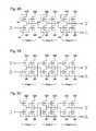
- FIG. 9Ashows examples of a CMOS inverter (I) which is conventionally used in general, and inverters (II) and (III) which are constituted by using TFTs of the polarity of any one of the N type and the P type.
- the inverter (II)is a TFT load-type inverter
- the inverter (III)is a resistance load-type inverter.
- FIG. 9Bshows a waveform of a signal inputted to the inverter.
- an input signal amplitudehas VDD-GND (GND ⁇ VDD).
- GND0 [V].
- VDD-GNDdenotes a range from a potential denoted by VDD to a potential denoted by GND.
- a range of the potentialsis referred by giving the symbol “-” in the middle of GND, VDD, and the like that denote each of the potentials.
- GND-VDD 1represents a range from the potential denoted by GND to the potential denoted by VDD 1 .
- a gate-source voltagethere is a case where the symbol “-” is given in the middle of a gate and a source.
- the gate-source voltagein this case denotes the voltage generated between a gate electrode and a source of a transistor and does not denote the range between the gate and the source.
- the operation of the TFT load-type inverter (II)will be described. Similarly a case where a signal as shown in FIG. 9B is inputted will be considered.
- an N-type TFT 904is turned OFF.
- a load TFT 903always operates under saturation condition, therefore the potential of an output node is raised in a direction of the H level.
- the N-type TFT 904is turned ON.
- the current capacity of the N-type TFT 904is made sufficiently higher than that of the load TFT 903 , so that the potential of the output node is lowered in a direction of the L level.
- the ON resistance value of an N-type TFT 906is made sufficiently lower than that of a load resistor 905 , when an input signal is at the H level, the N-type TFT 906 is turned ON, so that the potential of an output node is lowered in a direction of the L level.
- the N-type TFT 906is turned OFF, so that the potential of the output node is raised in a direction of the H level.
- FIG. 9Dshows an output waveform of the TFT load-type inverter.
- the potentialbecomes lower than VDD by the amount denoted by numeral 907 .
- the load TFT 903when a terminal of an output node side is a source, and a terminal of a power source VDD side is a drain, a gate electrode and a drain region are connected to each other. Therefore, the potential of the gate electrode at this time is VDD.
- the gate-source voltage of the TFT 903is larger than VthN, resulting in that the potential of the output node rises to at most a value (VDD ⁇ VthN) obtained by subtracting VthN from VDD. That is, the value denoted by numeral 907 is equal to VthN. Further, according to the ratio of the current capacity of the load TFT 903 to that of the N-type TFT 904 , when the output potential is at the L level, the potential becomes higher than GND by the amount denoted by numeral 908 .
- FIG. 9Eshows an output waveform of the resistance load type inverter.
- the potentialbecomes high by the amount indicated by numeral 909 . That is, when the inverter constituted by the TFTs of only one polarity shown here is employed, amplitude attenuation of the output signal occurs relative to the amplitude of the input signal. In order to form the driving circuit, the output has to be obtained without attenuating the amplitude.
- the present inventionhas been made in view of the above problem, and an object of the invention is to provide a semiconductor device (a driving circuit of a display device) which can be fabricated at low costs by using TFTs of only one polarity of either of an N type or a P type to reduce manufacturing steps and which can obtain an output without amplitude attenuation.
- an absolute value of a gate-source voltage of the N-type TFT 101has only to always exceed VthN. That is, in order to satisfy the condition under which the H level of the output node becomes VDD, the potential of the gate electrode of the N-type TFT 101 has to be set higher than a value (VDD+VthN) obtained by adding the potential of the power source VDD to that of the threshold value VthN.
- the power source supplied to the circuitincludes only two kinds such as VDD and GND. Therefore, if there is no third power source having a potential higher than VDD, the condition can not be satisfied.
- a capacitance 103is provided between the gate and the source of the N-type TFT 101 .
- the gate electrode of the N-type TFT 101has some potential and is brought into a floating state, and then the potential of the output node is raised, resulting in that with the rise of the potential of the output node, the potential of the gate electrode of the N-type TFT 101 is also raised by capacitance coupling with the capacitance 103 .
- a capacitance portionmay be actually fabricated, or a parasitic capacitance between the gate and the source of the TFT 101 may be used.
- a semiconductor deviceis characterized by comprising: a first transistor having a first impurity region connected to a first power source; a second transistor having a first impurity region connected to a second power source; a third transistor having a first impurity region connected to the first power source; and a fourth transistor having a first impurity region connected to the second power source, wherein: the first to fourth transistors have a same conductivity type; a second impurity region of the first transistor and a second impurity region of the second transistor are connected to one terminal of a capacitance; a second impurity region of the third transistor, a second impurity region of the fourth transistor, and a gate electrode of the first transistor are connected to the other terminal of the capacitance; a gate electrode of the second transistor and a gate electrode of the fourth transistor are connected to an input signal line; and a gate electrode of the third transistor is connected to the first power source.
- a semiconductor deviceis characterized by comprising: a first transistor having a first impurity region connected to a first power source; a second transistor having a first impurity region connected to a second power source; a third transistor having a first impurity region connected to the first power source; a fourth transistor having a first impurity region connected to the second power source; and a capacitance, wherein: the first to fourth transistors have a same conductivity type; a second impurity region of the first transistor and a second impurity region of the second transistor are connected to one terminal of the capacitance; a second impurity region of the third transistor, a second impurity region of the fourth transistor, and a gate electrode of the first transistor are connected to the other terminal of the capacitance; a gate electrode of the second transistor and a gate electrode of the fourth transistor are connected to a first input signal line; and a gate electrode of the third transistor is connected to a second input signal line.
- FIGS. 1A and 1Bare views for explaining the operation principle of a semiconductor device (a driving circuit of a display device) of the present invention.
- FIGS. 2A to 2 Dare views showing an inverter of a basic mode of a semiconductor device (a driving circuit of a display device) of the present invention and waveforms of its input/output signals.
- FIGS. 3A to 3 Care views showing connection examples in which an inverter of a basic mode of a semiconductor device (a driving circuit of a display device) of the present invention is used by connecting a plurality of stages thereof.
- FIGS. 4A to 4 Dare views showing a level shifter shown as an example of a semiconductor device (a driving circuit of a display device) of the present invention and waveforms of its input/output signals.
- FIGS. 5A and 5Bare views for explaining the operation of a level shifter and showing a structural example of the level shifter, respectively.
- FIG. 6is a view showing a structural example of a two-input type level shifter in a case where an inversion signal is included.
- FIG. 7is a schematic view showing a display device fabricated by applying the present invention.
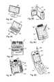
- FIGS. 8A to 8 Gare views showing examples of electronic equipment to which a semiconductor device (a driving circuit of a display device) of the present invention is applied.
- FIGS. 9A to 9 Eare views showing structures of a conventional CMOS inverter and load type inverters, and waveforms of respective input/output signals.
- FIGS. 10A and 10Bare views for explaining input signals and circuit operations of a four-TFT type inverter and a three-TFT type inverter.
- FIG. 2Ashows an embodiment of a semiconductor device (a driving circuit of a display device) of the present invention, which is a circuit functioning as an inverter.
- the circuitis constituted by N-type TFTs 201 to 204 , and a capacitance 205 , and a portion surrounded by a dotted line frame 206 is equivalent to the circuit shown in FIG. 1A.
- a portion surrounded by a dotted line frame 210forms an output amplitude compensating circuit.
- the output amplitude compensating circuit 210is formed for bringing a floating state to a gate electrode of the N-type TFT 203 , and as long as the same function is obtained, the circuit is not limited to the structure of FIG. 2 A.
- an input signalis inputted to gate electrodes of the N-type TFT 202 and the N-type TFT 204 .
- the N-type TFT 201functions as a load, and an output given from a circuit constituted by the N-type TFTs 201 and 202 is inputted to the gate electrode of the N-type TFT 203 .
- ⁇an output node given from the circuit constituted by the N-type TFTs 201 and 202 is referred as ⁇ .
- VDDpower source potentials
- GNDthe amplitude of an input signal
- L levelthe amplitude of an input signal
- the N-type TFTs 202 and 204are turned ON.
- the N-type TFT 201operates in a saturated state, however, the current capacity of the N-type TFT 202 is set sufficiently higher than the current capacity of the N-type TFT 201 , resulting in that the potential of the node ⁇ is lowered to the GND. Accordingly, the N-type TFT 203 is turned OFF, and the output of the L level appears at the output node.
- the N-type TFTs 202 and 204are turned OFF.
- the potential of the node ais raised to the VDD side, and when the potential becomes the value (Vdd ⁇ VthN) obtained by subtracting the threshold value VthN from the power source VDD, the floating state is once obtained.
- the N-type TFT 203is turned ON before long, and the potential of the output node is raised to the VDD side.
- the node ⁇is brought into the floating state, the potential of the output node remains to continue its rise.
- the potential of the node ⁇ in the floating statealso rises by the existence of the gate-source capacitance 205 of the N-type TFT 203 . Accordingly, the potential of the node a is allowed to be higher than a value (VDD+VthN) obtained by adding the power source VDD and the threshold value VthN. Thus, the output of the H level appears at the output node, and the potential at this time becomes equal to VDD.
- FIG. 2Bshows a waveform of the input signal of the circuit shown in FIG. 2A
- FIG. 2Cshows a waveform of the potential at the node a
- FIG. 2Dshows a waveform of the output signal.
- a potential denoted by numeral 208is a potential (VDD ⁇ VthN) which is lower than VDD by VthN
- the potential of the node ⁇is raised by the amount denoted by numeral 207 through the bootstrap.
- FIGS. 10A and 10Bshow structural examples of circuits using the bootstrap method.
- FIG. 10Ashows a basic structure of a semiconductor device (a driving circuit of a display device) of the present invention, in which a node a is in a floating state, to thereby raise the potential of the node a by using a gate-source capacitance 1005 of a TFT 1003 , and then compensate the amplitude of an output signal by that.
- FIG. 10Ashows a basic structure of a semiconductor device (a driving circuit of a display device) of the present invention, in which a node a is in a floating state, to thereby raise the potential of the node a by using a gate-source capacitance 1005 of a TFT 1003 , and then compensate the amplitude of an output signal by that.
- FIG. 10Ashows a basic structure of a semiconductor device (a driving circuit of a display device) of the present invention, in which a node a is in a floating state, to
- FIG. 10Bshows a circuit constituted by three TFTs, and similarly, in which a node ⁇ is in a floating state, to thereby raise the potential of the node ⁇ by using a gate-source capacitance 1009 of the TFT 1007 , and then compensate the amplitude of an output signal by that.
- VDDa power source potential at a high potential side
- GNDa power source potential at a low potential side
- inban inversion signal of the input signal
- the power source GND, the power source VDD 3 , the power source VDD, the threshold value VthN, and the value (VDD ⁇ VthN) obtained by subtracting the threshold value VthN from the power source VDDsatisfy the relation of GND ⁇ VthN ⁇ VDD 3 ⁇ (VDD ⁇ VthN).
- the potential of the gate electrode of the N-type TFT 1001becomes VDD 3 .
- VthN ⁇ VDD 3is satisfied, with the result that the N-type TFT 1001 is turned ON, the potential of the node ⁇ is raised to the VDD side, and then the floating state is obtained when the potential becomes the value (VDD 3 ⁇ VthN) obtained by subtracting the threshold value VthN from the power source VDD 3 . That is, if the H level of the signal inb exceeds VthN, the node ⁇ can be securely brought into the floating state, and the operation of raising the potential of the gate electrode of the N-type TFT 1003 is enabled by the bootstrap. On the other hand, in FIG. 10B , the potential of the gate electrode of the N-type TFT 1006 is always VDD.
- the potential of the node ⁇is raised to VDD 3 .
- VDD 3 ⁇ (VDD ⁇ VthN)is satisfied, resulting in that the N-type TFT 1006 always takes the ON state irrespective of the potential of the input signal.
- the node ⁇does not enter the floating state. Accordingly, the potential of the node ⁇ can not be raised by the bootstrap. That is, in the case of the circuit shown in FIG. 10B , in order that the node ⁇ enters the floating state, there is a minimum condition under which at least the H level is not lower than (VDD ⁇ VthN) when the L level of the signal inb is GND. Accordingly, it is disadvantageous in view of low voltage driving and fluctuation in characteristics of TFTs.
- the present inventionhaving the structure as described above can provide a semiconductor device which can be fabricated at low cost by using TFTs of only one polarity of either of the N type or the P type to reduce the manufacturing steps and which can obtain the output without amplitude attenuation.
- circuits in which a plurality of stages of inverters are connected using the present inventionwill be described with reference to FIGS. 3A to 3 C.
- FIG. 3Ashows a circuit in which a plurality of stages of inverters each of which is a mode of a semiconductor device (a driving circuit of a display device) of the present invention are connected.
- a driving circuit of the display device or the likesuch a circuit is often used as a buffer.
- manufacturing stepsare reduced by using TFTs of only one polarity of either of the N type or the P type, so that it can be fabricated at low cost. Further, an output without amplitude attenuation can be obtained.
- the circuit as shown in FIG. 3Ais employed, the following point should be noted in view of consumed electric power of the circuit.
- an N-type TFT 302when an input signal is at the H level, an N-type TFT 302 is turned ON.
- an N-type TFT 301functions as a load in which its gate and drain are short-circuited, and always operates in saturation.
- a through currentflows between VDD and GND.
- TFTs 303 , 304 and 305 , 306 of respective stagesAs a result, consumed current becomes large.
- a method of using a two-input type invertercan be mentioned.
- TFTs arranged between VDD and GNDpolarities of input signals are always opposite to each other. Therefore, an exclusive operation is carried out, so that a through current does not flow.
- the one-input type inverter of the present inventionis used for the first stage, and the two-input type inverters are used for the second stage and the following.
- the output signal of the former stageis inputted as one of them, and the input signal of the former stage is inputted as the other.
- the circuitcan be used as a buffer which is of one-input type and in which the through current is suppressed to a minimum.
- the manufacturing stepscan be reduced by using the TFTs of only one polarity of either of the N type or the P type, it can be fabricated at low cost, and the output without amplitude attenuation can be obtained.
- a semiconductor device (a driving circuit of a display device) of the present inventioncan easily function as a level shifter by giving a potential which is different from an amplitude potential of an input signal as a power source potential supplied to a circuit. An example will be described below.
- FIG. 4Ashows an example.
- the structure of a circuitmay be the same as the embodiment and the example 1.
- the amplitude of an input signalhas GND-VDD 1 , and potentials of power sources connected to ends of impurity regions of N-type TFTs 401 and 403 are referred as VDD 2 .
- FIG. 4Bshows a waveform of an input signal.
- the signal having an amplitude of GND-VDD 1is inputted to gate electrodes of N-type TFTs 402 and 404 .
- the N-type TFTs 402 and 404are turned ON, the potential at a node a is lowered to the GND side, and the N-type TFT 403 is turned OFF.
- the potential at the output nodecomes to have the L level.
- the N-type TFTs 402 and 404are turned OFF, and the potential at the node a is raised to the VDD 2 side. Accordingly, the N-type TFT 403 is turned ON, and the potential of the output node rises.
- the potentialbecomes the value (VDD 2 ⁇ absolute value of threshold voltage of the N-type TFT 403 ) obtained by subtracting the absolute value of the threshold voltage of the N-type TFT 403 from the power source VDD 2 , it is brought into the floating state.
- the potential of the output noderises, the potential of the node ⁇ is further raised by a capacitance coupling 405 existing between the gate and source of the N-type TFT 403 , and then takes a potential higher than VDD 2 (FIG. 4 C).
- the potential of the output nodecomes to have the H level, and the signal having the amplitude of GND-VDD 2 is outputted (a solid line of FIG. 4 D).
- the circuit shown in this examplecan be easily used as the level shifter, it is possible to mention a point that a signal input of a low voltage amplitude is not applied to gate electrodes of the TFTs 401 and 403 connected to the high potential side power source (VDD 2 ).
- VDD 2high potential side power source
- a TFT 503can not be sufficiently turned ON as well, and the gate electrode potential of the TFT 503 can not be raised by using capacitance coupling, so that a normal operation thereof can not be achieved.
- TFTs to which a signal of a low voltage amplitude is inputtedare limited to TFTs of a portion surrounded by a dotted line frame 506 , and when two stages of one-input type circuits are connected, signals of high voltage amplitudes are inputted to two inputs (inputs to gate electrodes of TFTs 507 and 508 ) of a third stage, so that the normal operation can be carried out.
- FIG. 6shows an example.
- Input signalsare denoted by “in” and “inb”, and are respectively inputted to gate electrodes of TFTs 602 and 614 .
- the output of a first stage level shifter 650is inputted to second stage TFTs 606 and 617
- the output of a first stage level shifter 660is inputted to second stage TFTs 605 and 618 .
- Both of the signals inputted to the second stageare ones of high voltage amplitudes, therefore, subsequent level shifters normally function as buffers, and then output signals “out” and “outb” are obtained from the final stage.
- the manufacturing stepscan be reduced by using the TFTs of only one polarity of either of the N type or the P type, resulting in that it can be fabricated at low cost, and the output without amplitude attenuation can be obtained.
- FIG. 7is a schematic view of a display device.
- a source signal line driving circuit 701 , a gate signal line driving circuit 702 , and a pixel portion 703are fabricated so as to be integrated on a substrate 700 .
- a portion surrounded by a dotted line 710illustrates one pixel.
- the example of FIG. 7shows a pixel of a liquid crystal display device, and one TFT (hereinafter referred to as a pixel TFT) controls an electric charge applied to one electrode of a liquid crystal element.
- Signal inputs to the source signal line driving circuit 701 and the gate signal line driving circuit 702are supplied from the outside through a flexible print circuit (FPC) 704 .
- FPCflexible print circuit
- the substrate having the pixel TFT and the driving circuitsmay be manufactured in accordance with a known method, for example, as disclosed in U.S. Pat. No. 5,889,291 issued to Koyama et al. Also, it is possible to crystallize a semiconductor film for an active layer of the TFTs by utilizing a metal element for promoting crystallization although other known methods can be used for crystallization. Such a method of using the metal element is disclosed, for example, in U.S. Pat. No. 5,643,826 issued to Ohtani et al. The entire disclosures of these U.S. Pat. Nos. 5,889,291 and 5,643,826 are incorporated herein by reference.
- the display device shown in this exampleis constructed by using the semiconductor device (the driving circuit of the display device) of the present invention, and the driving circuits constituting the whole display device including the pixel portions are fabricated by using only TFTs (for example, N-type TFTs) of one polarity same as that of the pixel TFT.
- TFTsfor example, N-type TFTs
- an ion doping step for giving the P type to a semiconductor layercan be omitted, and this can contribute to a reduction in manufacturing cost and an improvement in yield.
- the polarity of the TFT constituting the display device of this exampleis the N type
- the present inventionneedless to say, it becomes possible to constitute the driving circuit and the pixel TFTs by using only P-type TFTs.
- an ion doping step to be omittedis one for giving the N type to a semiconductor layer.
- the present inventioncan be applied to not only the liquid crystal display device but also any device as long as it is fabricated by integrally forming a driving circuit on an insulator.
- a semiconductor device (a driving circuit of a display device) of the present inventioncan be applied to fabrication of a display device used for various electronic equipment.
- Such electronic equipmentincludes a portable information terminal (electronic notebook, mobile computer, portable telephone, etc.), a video camera, a digital camera, a personal computer, a television, a portable telephone, and the like.
- FIGS. 8A to 8 Gshow examples of those.
- FIG. 8Ashows a liquid crystal display (LCD) which is constituted by a housing 3001 , a supporting stand 3002 , a display portion 3003 , and the like.
- the semiconductor device (the driving circuit of the display device) of the present inventioncan be applied to the fabrication of the display portion 3003 .
- FIG. 8Bshows a video camera which is constituted by a main body 3011 , a display portion 3012 , an audio input portion 3013 , an operation switch 3014 , a battery 3015 , an image receiving portion 3016 , and the like.
- the semiconductor device (the driving circuit of the display device) of the present inventioncan be applied to the fabrication of the display portion 3012 .
- FIG. 8Cshows a notebook personal computer which is constituted by a main body 3021 , a housing 3022 , a display portion 3023 , a keyboard 3024 , and the like.
- the semiconductor device (the driving circuit of the display device) of the present inventioncan be applied to the fabrication of the display portion 3023 .
- FIG. 8Dshows a portable information terminal which is constituted by a main body 3031 , a stylus 3032 , a display portion 3033 , an operation button 3034 , an external interface 3035 , and the like.
- the semiconductor device (the driving circuit of the display device) of the present inventioncan be applied to the fabrication of the display portion 3033 .
- FIG. 8Eshows a sound reproducing system, specifically an on-vehicle audio apparatus, which is constituted by a main body 3041 , a display portion 3042 , operation switches 3043 and 3044 , and the like.
- the semiconductor device (the driving circuit of the display device) of the present inventioncan be applied to the fabrication of the display portion 3042 .
- the on-vehicle audio apparatusis illustrated in this example, the invention can also be used for a portable or household audio apparatus.
- FIG. 8Fshows a digital camera which is constituted by a main body 3051 , a display portion (A) 3052 , an eyepiece portion 3053 , an operation switch 3054 , a display portion (B) 3055 , a battery 3056 , and the like.
- the semiconductor device (the driving circuit of the display device) of the present inventioncan be applied to the fabrication of the display portion (A) 3052 and the display portion (B) 3055 .
- FIG. 8Gshows a portable telephone which is constituted by a main body 3061 , an audio output portion 3062 , an audio input portion 3063 , a display portion 3064 , an operation switch 3065 , an antenna 3066 , and the like.
- the semiconductor device (the driving circuit of the display device) of the present inventioncan be applied to the fabrication of the display portion 3064 .
- the semiconductor device (the driving circuit of the display device) of the present inventionit becomes possible to constitute a driving circuit of a display device and a pixel portion of a display device by use of only TFTs of one conductivity type. Also, fabricating steps of the display device are reduced, to thereby contribute to a reduction in cost and an improvement in yield. As a result, the display device can be supplied more inexpensively. Further, by employing the present invention, the semiconductor device capable of obtaining the output without amplitude attenuation can be provided.
Landscapes
- Physics & Mathematics (AREA)
- Engineering & Computer Science (AREA)
- Computer Hardware Design (AREA)
- Mathematical Physics (AREA)
- Computing Systems (AREA)
- General Engineering & Computer Science (AREA)
- General Physics & Mathematics (AREA)
- Nonlinear Science (AREA)
- Crystallography & Structural Chemistry (AREA)
- Theoretical Computer Science (AREA)
- Chemical & Material Sciences (AREA)
- Optics & Photonics (AREA)
- Control Of Indicators Other Than Cathode Ray Tubes (AREA)
- Thin Film Transistor (AREA)
- Liquid Crystal Display Device Control (AREA)
- Liquid Crystal (AREA)
- Logic Circuits (AREA)
- Shift Register Type Memory (AREA)
- Metal-Oxide And Bipolar Metal-Oxide Semiconductor Integrated Circuits (AREA)
- Electronic Switches (AREA)
- Electroluminescent Light Sources (AREA)
Abstract
Description
1. Field of the Invention
The present invention relates to a semiconductor device. The semiconductor device means any device which can function by using semiconductor characteristics. Further, the present invention relates to a driving circuit of a display device. Additionally, the present invention includes electronic equipment fabricated by using the driving circuit of the display device. Note that, in the present specification, the display device includes a liquid crystal display device obtained by using a liquid crystal element for a pixel, and a light emitting display device obtained by using a self-luminous element such as an organic electroluminescence (EL) element or the like. The driving circuit means a circuit for carrying out a processing to input image signals to pixels arranged in the display device and to display an image, and includes a pulse circuit such as a shift register or the like, and an amplifying circuit such as an amplifier or the like.
2. Description of the Related Art
In recent years, a semiconductor device (a display device) in which a semiconductor thin film is formed on an insulator, especially on a glass substrate, especially an active matrix type display device using a thin film transistor (hereinafter referred to as a TFT) has come into wide use remarkably. The active matrix type display device using the TFT includes hundreds of thousands to millions of pixels which are arranged so as to be formed into a matrix shape, and an electric charge of each of the pixels is controlled by a TFT arranged in each of the pixels, so that an image is displayed.
Further, as a recent technique, a technique relating to a polysilicon TFT in which a driving circuit is simultaneously formed using TFTs in a region around a pixel portion, in addition to a pixel TFT constituting a pixel, has been developed, which greatly contributes to the miniaturization of a device and the reduction in consumed electric power, and as a result of that, the display device becomes an indispensable device for a display portion etc. of a mobile information terminal an application field of which is remarkably expanded in recent years.
As the semiconductor device (the driving circuit of the display device), a CMOS circuit in which an N-type TFT and a P-type TFT are combined is usually employed. The CMOS circuit is characterized by the following two points: a current flows only at an instant when a logic is changed and a current does not flow during a period in which a certain logic is held; and a current flows only at an instant when a logic is changed and there is only a minute leak current during a period in which a certain logic is held (although the preferable leak current is zero). The CMOS circuit has the foregoing two characteristics, thus the CMOS circuit has advantages such that the consumed current in the whole circuit can be reduced, and high speed driving can be excellently performed.
Note that, the term “logic” indicates an H level or an L level. Also, the term “logic change” indicates that the H level is changed to the L level or the L level is changed to the H level.
As mobile electronic equipment is miniaturized and is reduced in weight, demand for a display device using liquid crystal or self-luminous elements is rapidly increased, however, from the viewpoint of the yield and the like, it is difficult to reduce the manufacturing cost to the level sufficiently low. It is easily supposed that the demand is further rapidly increased in future, and accordingly, it is desired that the display device can be supplied more inexpensively.
As a method of fabricating a driving circuit on an insulator, there is a common method in which patterns of active layers, wiring lines and the like are formed through exposure treatment and etching with a plurality of photomasks. However, the number of steps during this processing directly influences the manufacturing cost, therefore it is ideal to manufacture the device at the number of the steps as small as possible. Then, the driving circuit, which is conventionally constituted by the CMOS circuit, is constituted by using TFTs the conductivity type of which belongs to either of the N type or the P type. With this method, a part of an ion doping step can be omitted, and the number of the photomasks can also be decreased.
However, if the driving circuit is constructed by using TFTs the conductivity type of which belongs to either of the N type or the P type, the following problem occurs. This problem will be explained below.
Note that, the foregoing term “VDD-GND” denotes a range from a potential denoted by VDD to a potential denoted by GND. In the present specification, a range of the potentials is referred by giving the symbol “-” in the middle of GND, VDD, and the like that denote each of the potentials. For example, GND-VDD1 represents a range from the potential denoted by GND to the potential denoted by VDD1. Also, in the present specification, as an exception such as a gate-source voltage, there is a case where the symbol “-” is given in the middle of a gate and a source. The gate-source voltage in this case denotes the voltage generated between a gate electrode and a source of a transistor and does not denote the range between the gate and the source.
A circuit operation will be explained. Note that, for clarification and simplification of the explanation, it is assumed that the threshold voltages of N-type TFTs constituting a circuit are not irregular and are uniformly defined as VthN. Similarly, the threshold voltages of P-type TFTs are uniformly defined as VthP.
When a signal as shown inFIG. 9B is inputted to the CMOS inverter in the state that the potential of the input signal is at the H level (VDD), a P-type TFT 901 is turned OFF and an N-type TFT 902 is turned ON, so that the potential of an output node comes to have the L level (GND). On the contrary, when the potential of the input signal is at the L level, the P-type TFT 901 is turned ON and the N-type TFT 902 is turned OFF, so that the potential of the output node comes to have the H level (FIG.9C).
Next, the operation of the TFT load-type inverter (II) will be described. Similarly a case where a signal as shown inFIG. 9B is inputted will be considered. First, when the input signal is at the L level, an N-type TFT 904 is turned OFF. On the other hand, aload TFT 903 always operates under saturation condition, therefore the potential of an output node is raised in a direction of the H level. On the other hand, when the input signal is at the H level, the N-type TFT 904 is turned ON. Here, the current capacity of the N-type TFT 904 is made sufficiently higher than that of theload TFT 903, so that the potential of the output node is lowered in a direction of the L level.
Also with respect to the resistance load-type inverter (III), similarly, if the ON resistance value of an N-type TFT 906 is made sufficiently lower than that of aload resistor 905, when an input signal is at the H level, the N-type TFT 906 is turned ON, so that the potential of an output node is lowered in a direction of the L level. When the input signal is at the L level, the N-type TFT 906 is turned OFF, so that the potential of the output node is raised in a direction of the H level.
However, when the TFT load type inverter or the resistance load-type inverter is used, there is a problem as described below.FIG. 9D shows an output waveform of the TFT load-type inverter. When the output is at the H level, the potential becomes lower than VDD by the amount denoted bynumeral 907. In theload TFT 903, when a terminal of an output node side is a source, and a terminal of a power source VDD side is a drain, a gate electrode and a drain region are connected to each other. Therefore, the potential of the gate electrode at this time is VDD. Also, under the condition allowing the load TFT in an ON state, the gate-source voltage of theTFT 903 is larger than VthN, resulting in that the potential of the output node rises to at most a value (VDD−VthN) obtained by subtracting VthN from VDD. That is, the value denoted bynumeral 907 is equal to VthN. Further, according to the ratio of the current capacity of theload TFT 903 to that of the N-type TFT 904, when the output potential is at the L level, the potential becomes higher than GND by the amount denoted bynumeral 908. In order to make this sufficiently close to GND, the current capacity of the N-type TFT 904 has to be set sufficiently high as compared with theload TFT 903. Similarly,FIG. 9E shows an output waveform of the resistance load type inverter. According to the ratio of the resistance value of theload resistor 905 to the ON resistance of the N-type TFT 906, the potential becomes high by the amount indicated bynumeral 909. That is, when the inverter constituted by the TFTs of only one polarity shown here is employed, amplitude attenuation of the output signal occurs relative to the amplitude of the input signal. In order to form the driving circuit, the output has to be obtained without attenuating the amplitude.
The present invention has been made in view of the above problem, and an object of the invention is to provide a semiconductor device (a driving circuit of a display device) which can be fabricated at low costs by using TFTs of only one polarity of either of an N type or a P type to reduce manufacturing steps and which can obtain an output without amplitude attenuation.
In the foregoing TFT load-type inverter (II) shown inFIG. 9A , consideration will be given to a condition under which the amplitude of the output signal normally takes VDD-GND. First, in a circuit as shown inFIG. 1A , when the potential of an output signal comes to have the L level, a resistance value between the power source GND and an output node has only to be sufficiently low as compared with a resistance value between the power source VDD and the output node so that the potential is caused sufficiently close to GND. That is, an N-type TFT 101 has only to be in an OFF state during a period in which an N-type TFT 102 is in an ON state. Second, when the potential of the output signal comes to have the H level, in order to cause the potential equal to VDD, an absolute value of a gate-source voltage of the N-type TFT 101 has only to always exceed VthN. That is, in order to satisfy the condition under which the H level of the output node becomes VDD, the potential of the gate electrode of the N-type TFT 101 has to be set higher than a value (VDD+VthN) obtained by adding the potential of the power source VDD to that of the threshold value VthN. The power source supplied to the circuit includes only two kinds such as VDD and GND. Therefore, if there is no third power source having a potential higher than VDD, the condition can not be satisfied.
Then, in the present invention, means as described below is devised. As shown inFIG. 1B , acapacitance 103 is provided between the gate and the source of the N-type TFT 101. The gate electrode of the N-type TFT 101 has some potential and is brought into a floating state, and then the potential of the output node is raised, resulting in that with the rise of the potential of the output node, the potential of the gate electrode of the N-type TFT 101 is also raised by capacitance coupling with thecapacitance 103. When this effect is used, it becomes possible to make the potential of the gate electrode of the N-type TFT 101 higher than VDD, more accurately, than the value (VDD+VthN) obtained by adding the potential of the power source VDD and the potential of the threshold value VthN. Thus, the potential of the output node is allowed to be raised sufficiently to VDD.
Note that, with respect to thecapacitance 103 shown inFIG. 1B , a capacitance portion may be actually fabricated, or a parasitic capacitance between the gate and the source of theTFT 101 may be used.
The structure of the present invention will be described hereinbelow.
A semiconductor device according to the present invention is characterized by comprising: a first transistor having a first impurity region connected to a first power source; a second transistor having a first impurity region connected to a second power source; a third transistor having a first impurity region connected to the first power source; and a fourth transistor having a first impurity region connected to the second power source, wherein: the first to fourth transistors have a same conductivity type; a second impurity region of the first transistor and a second impurity region of the second transistor are connected to one terminal of a capacitance; a second impurity region of the third transistor, a second impurity region of the fourth transistor, and a gate electrode of the first transistor are connected to the other terminal of the capacitance; a gate electrode of the second transistor and a gate electrode of the fourth transistor are connected to an input signal line; and a gate electrode of the third transistor is connected to the first power source.
A semiconductor device according to the present invention is characterized by comprising: a first transistor having a first impurity region connected to a first power source; a second transistor having a first impurity region connected to a second power source; a third transistor having a first impurity region connected to the first power source; a fourth transistor having a first impurity region connected to the second power source; and a capacitance, wherein: the first to fourth transistors have a same conductivity type; a second impurity region of the first transistor and a second impurity region of the second transistor are connected to one terminal of the capacitance; a second impurity region of the third transistor, a second impurity region of the fourth transistor, and a gate electrode of the first transistor are connected to the other terminal of the capacitance; a gate electrode of the second transistor and a gate electrode of the fourth transistor are connected to a first input signal line; and a gate electrode of the third transistor is connected to a second input signal line.
In the circuit ofFIG. 2A , an input signal is inputted to gate electrodes of the N-type TFT 202 and the N-type TFT 204. The N-type TFT 201 functions as a load, and an output given from a circuit constituted by the N-type TFTs type TFT 203. Note that, inFIG. 2A , an output node given from the circuit constituted by the N-type TFTs
The operation of the circuit will be described in sequence. Note that, power source potentials are referred as VDD and GND, and the amplitude of an input signal is referred as VDD (H level)-GND (L level). First, when the potential of the input signal is at the H level, the N-type TFTs type TFT 201 operates in a saturated state, however, the current capacity of the N-type TFT 202 is set sufficiently higher than the current capacity of the N-type TFT 201, resulting in that the potential of the node α is lowered to the GND. Accordingly, the N-type TFT 203 is turned OFF, and the output of the L level appears at the output node.
Subsequently, when the potential of the input signal is at the L level, the N-type TFTs type TFT 203 is turned ON before long, and the potential of the output node is raised to the VDD side. When the node α is brought into the floating state, the potential of the output node remains to continue its rise. Therefore, as the potential of the output node is raised, the potential of the node α in the floating state also rises by the existence of the gate-source capacitance 205 of the N-type TFT 203. Accordingly, the potential of the node a is allowed to be higher than a value (VDD+VthN) obtained by adding the power source VDD and the threshold value VthN. Thus, the output of the H level appears at the output node, and the potential at this time becomes equal to VDD.
By the above operation, the amplitude of the output signal can be obtained without attenuation relative to the amplitude of the input signal. A method of raising the potential by using the capacitance coupling that is conducted between two positions as stated above is called a bootstrap method.FIG. 2B shows a waveform of the input signal of the circuit shown inFIG. 2A ,FIG. 2C shows a waveform of the potential at the node a, andFIG. 2D shows a waveform of the output signal. InFIG. 2C , a potential denoted bynumeral 208 is a potential (VDD−VthN) which is lower than VDD by VthN, and the potential of the node α is raised by the amount denoted by numeral207 through the bootstrap. As a result, as shown inFIG. 2D , when the output node is at the H level, the potential rises to VDD, and the output signal having the amplitude of VDD-GND can be obtained.
In the semiconductor device (the driving circuit of the display device) of the present invention, although the amplitude compensation of the output signal that is carried out by the bootstrap method is constructed as the base of the operation, at that time, it is assumed that the gate electrode of the TFT using the capacitance coupling is in the floating state.FIGS. 10A and 10B show structural examples of circuits using the bootstrap method.FIG. 10A shows a basic structure of a semiconductor device (a driving circuit of a display device) of the present invention, in which a node a is in a floating state, to thereby raise the potential of the node a by using a gate-source capacitance 1005 of aTFT 1003, and then compensate the amplitude of an output signal by that.FIG. 10B shows a circuit constituted by three TFTs, and similarly, in which a node β is in a floating state, to thereby raise the potential of the node β by using a gate-source capacitance 1009 of theTFT 1007, and then compensate the amplitude of an output signal by that.
Next, consideration will be given to the amplitude of an input signal and a power source potential. Now, a power source potential at a high potential side is referred as VDD; a power source potential at a low potential side, GND; the amplitude of an input signal (in), VDD-GND; and inb, an inversion signal of the input signal. Here, consideration will be given to the states of the node α and the node β in the case where the amplitudes of the signals in and inb have respectively VDD3-GND. The power source GND, the power source VDD3, the power source VDD, the threshold value VthN, and the value (VDD−VthN) obtained by subtracting the threshold value VthN from the power source VDD satisfy the relation of GND<VthN<VDD3<(VDD−VthN). InFIG. 10A , when the signal inb is at the H level, the potential of the gate electrode of the N-type TFT 1001 becomes VDD3. VthN<VDD3 is satisfied, with the result that the N-type TFT 1001 is turned ON, the potential of the node α is raised to the VDD side, and then the floating state is obtained when the potential becomes the value (VDD3−VthN) obtained by subtracting the threshold value VthN from the power source VDD3. That is, if the H level of the signal inb exceeds VthN, the node α can be securely brought into the floating state, and the operation of raising the potential of the gate electrode of the N-type TFT 1003 is enabled by the bootstrap. On the other hand, inFIG. 10B , the potential of the gate electrode of the N-type TFT 1006 is always VDD. Therefore, when the signal inb is at the H level, the potential of the node β is raised to VDD3. However, now, VDD3<(VDD−VthN) is satisfied, resulting in that the N-type TFT 1006 always takes the ON state irrespective of the potential of the input signal. Thus, the node β does not enter the floating state. Accordingly, the potential of the node β can not be raised by the bootstrap. That is, in the case of the circuit shown inFIG. 10B , in order that the node β enters the floating state, there is a minimum condition under which at least the H level is not lower than (VDD−VthN) when the L level of the signal inb is GND. Accordingly, it is disadvantageous in view of low voltage driving and fluctuation in characteristics of TFTs.
As stated above, in the case where the amplitude of an input signal is smaller than a power source voltage, under a certain specific condition, there is a fear that the floating state can not be given to the node β in the structure as shown in FIG.10B. On the other hand, in the structure of the present invention shown inFIG. 10A , there is a merit that enables the node α to securely bring into the floating state.
The present invention having the structure as described above can provide a semiconductor device which can be fabricated at low cost by using TFTs of only one polarity of either of the N type or the P type to reduce the manufacturing steps and which can obtain the output without amplitude attenuation.
Hereinafter, examples of the present invention will be described.
In this example, circuits in which a plurality of stages of inverters are connected using the present invention will be described with reference toFIGS. 3A to3C.
InFIG. 3A , when an input signal is at the H level, an N-type TFT 302 is turned ON. Here, an N-type TFT 301 functions as a load in which its gate and drain are short-circuited, and always operates in saturation. Thus, when the N-type TFT 302 is turned ON, a through current flows between VDD and GND. The same applies to TFTs303,304 and305,306 of respective stages. As a result, consumed current becomes large.
As an example for avoiding such a problem, as shown inFIG. 3B , a method of using a two-input type inverter can be mentioned. In the case of such a circuit, in TFTs arranged between VDD and GND, polarities of input signals are always opposite to each other. Therefore, an exclusive operation is carried out, so that a through current does not flow.
However, in the case where the circuit ofFIG. 3B is used, it is necessary to prepare two-phase signals of inversion and non-inversion as input signals.
Then, as the configuration of combination of both the semiconductor device shown in FIG.3A and the semiconductor device shown inFIG. 3B , as shown inFIG. 3C , the one-input type inverter of the present invention is used for the first stage, and the two-input type inverters are used for the second stage and the following. As the inputs of the second stage, the output signal of the former stage is inputted as one of them, and the input signal of the former stage is inputted as the other. Thus, the circuit can be used as a buffer which is of one-input type and in which the through current is suppressed to a minimum.
In the semiconductor device of the present invention having the structure as described above, since the manufacturing steps can be reduced by using the TFTs of only one polarity of either of the N type or the P type, it can be fabricated at low cost, and the output without amplitude attenuation can be obtained.
A semiconductor device (a driving circuit of a display device) of the present invention can easily function as a level shifter by giving a potential which is different from an amplitude potential of an input signal as a power source potential supplied to a circuit. An example will be described below.
First, as power source potentials, three potentials such as GND, VDD1, and VDD2 are considered, and it is assumed that they have the magnitude relation of GND<VDD1<VDD2. At this time, consideration will be given to a case where a signal having an amplitude of GND-VDD1 is inputted and is converted into a signal having an amplitude of GND-VDD2, and then the signal is extracted.
The operation of the circuit will be described.FIG. 4B shows a waveform of an input signal. The signal having an amplitude of GND-VDD1 is inputted to gate electrodes of N-type TFTs type TFTs type TFT 403 is turned OFF. Thus, the potential at the output node comes to have the L level.
When the input signal is at the L level, the N-type TFTs type TFT 403 is turned ON, and the potential of the output node rises. On the other hand, at the node α, when the potential becomes the value (VDD2−absolute value of threshold voltage of the N-type TFT403) obtained by subtracting the absolute value of the threshold voltage of the N-type TFT 403 from the power source VDD2, it is brought into the floating state. Thereafter, as the potential of the output node rises, the potential of the node α is further raised by acapacitance coupling 405 existing between the gate and source of the N-type TFT 403, and then takes a potential higher than VDD2 (FIG.4C). Thus, the potential of the output node comes to have the H level, and the signal having the amplitude of GND-VDD2 is outputted (a solid line of FIG.4D).
As the reason why the circuit shown in this example can be easily used as the level shifter, it is possible to mention a point that a signal input of a low voltage amplitude is not applied to gate electrodes of theTFTs FIG. 5A , even if a signal of a low voltage amplitude is inputted to aTFT 501 connected to a high potential side power source (VDD2), the potential of a node can rise at most to the vicinity of VDD1. Accordingly, aTFT 503 can not be sufficiently turned ON as well, and the gate electrode potential of theTFT 503 can not be raised by using capacitance coupling, so that a normal operation thereof can not be achieved.
Thus, in the case where heavy load is applied immediately after the level shifter shown in this example and a structure such as a buffer is required, as shown inFIG. 5B , it is necessary that two stages of one-input type circuits are used and all amplitudes of input signals thereafter are made high voltage amplitudes. InFIG. 5B , TFTs to which a signal of a low voltage amplitude is inputted are limited to TFTs of a portion surrounded by a dottedline frame 506, and when two stages of one-input type circuits are connected, signals of high voltage amplitudes are inputted to two inputs (inputs to gate electrodes ofTFTs 507 and508) of a third stage, so that the normal operation can be carried out.
In the case where signals for performing amplitude conversion include inverted signals, a structure may be adopted in which mutual output signals are used as inverted inputs of a next stage.FIG. 6 shows an example. Input signals are denoted by “in” and “inb”, and are respectively inputted to gate electrodes ofTFTs stage level shifter 650 is inputted tosecond stage TFTs stage level shifter 660 is inputted tosecond stage TFTs
In the semiconductor device of the present invention having the structure as described above, the manufacturing steps can be reduced by using the TFTs of only one polarity of either of the N type or the P type, resulting in that it can be fabricated at low cost, and the output without amplitude attenuation can be obtained.
In this example, a description will be given on an example in which a display device is fabricated by using a semiconductor device (a driving circuit of a display device) of the present invention.
The substrate having the pixel TFT and the driving circuits may be manufactured in accordance with a known method, for example, as disclosed in U.S. Pat. No. 5,889,291 issued to Koyama et al. Also, it is possible to crystallize a semiconductor film for an active layer of the TFTs by utilizing a metal element for promoting crystallization although other known methods can be used for crystallization. Such a method of using the metal element is disclosed, for example, in U.S. Pat. No. 5,643,826 issued to Ohtani et al. The entire disclosures of these U.S. Pat. Nos. 5,889,291 and 5,643,826 are incorporated herein by reference.
The display device shown in this example is constructed by using the semiconductor device (the driving circuit of the display device) of the present invention, and the driving circuits constituting the whole display device including the pixel portions are fabricated by using only TFTs (for example, N-type TFTs) of one polarity same as that of the pixel TFT. Thus, an ion doping step for giving the P type to a semiconductor layer can be omitted, and this can contribute to a reduction in manufacturing cost and an improvement in yield.
Although the polarity of the TFT constituting the display device of this example is the N type, according to the present invention, needless to say, it becomes possible to constitute the driving circuit and the pixel TFTs by using only P-type TFTs. In this case, an ion doping step to be omitted is one for giving the N type to a semiconductor layer. Also, the present invention can be applied to not only the liquid crystal display device but also any device as long as it is fabricated by integrally forming a driving circuit on an insulator.
A semiconductor device (a driving circuit of a display device) of the present invention can be applied to fabrication of a display device used for various electronic equipment. Such electronic equipment includes a portable information terminal (electronic notebook, mobile computer, portable telephone, etc.), a video camera, a digital camera, a personal computer, a television, a portable telephone, and the like.FIGS. 8A to8G show examples of those.
Note that, the examples set forth above are merely examples, and the present invention is not limited to these applications.
According to the semiconductor device (the driving circuit of the display device) of the present invention, it becomes possible to constitute a driving circuit of a display device and a pixel portion of a display device by use of only TFTs of one conductivity type. Also, fabricating steps of the display device are reduced, to thereby contribute to a reduction in cost and an improvement in yield. As a result, the display device can be supplied more inexpensively. Further, by employing the present invention, the semiconductor device capable of obtaining the output without amplitude attenuation can be provided.
Claims (23)
1. A semiconductor device comprising:
a first thin film transistor having a first impurity region electrically connected to a first power source;
a second thin film transistor having a first impurity region electrically connected to a second power source;
a third thin film transistor having a first impurity region electrically connected to the first power source;
a fourth thin film transistor having a first impurity region electrically connected to the second power source,
wherein:
the first to fourth thin film transistors have a same conductivity type;
a second impurity region of the first thin film transistor and a second impurity region of the second thin film transistor are electrically connected to one terminal of a capacitance;
a second impurity region of the third thin film transistor, a second impurity region of the fourth thin film transistor, and a gate electrode of the first thin film transistor are electrically connected to the other terminal of the capacitance;
a gate electrode of the second thin film transistor and a gate electrode of the fourth thin film transistor are electrically connected to a first input signal line; and
a gate electrode of the third thin film transistor is electrically connected to a second input signal line.
2. The semiconductor device according toclaim 1 , wherein the second input signal line is the signal line to which an inversion signal of a signal inputted to the first input signal line is inputted.
3. The semiconductor device according toclaim 1 , wherein the capacitance uses a capacitance between the gate electrode of the first thin film transistor and one of the impurity regions.
4. The semiconductor device according toclaim 1 , wherein the capacitance is a capacitance constituted by using any two materials of an active layer material, a material forming the gate electrodes, and a wiring material.
5. The semiconductor device according toclaim 1 , wherein the one conductivity is an N-channel type.
6. The semiconductor device according toclaim 1 , wherein the one conductivity is a P-channel type.
7. The semiconductor device according toclaim 1 , wherein:
the one conductivity is an N-channel type;
a potential at a time when the input signal is at an H level is equal to a third power source potential, and a potential at a time when the input signal is at an L level is equal to a fourth power source potential; and
a relation of a second power source potential≦the fourth power source potential<the third power source potential≦a first power source potential is satisfied.
8. The semiconductor device according toclaim 1 , wherein:
the one conductivity is a P-channel type;
a potential at a time when the input signal is at a H level is equal to a third power source potential, and a potential at a time when the input signal is at a L level is equal to a fourth power source potential; and
a relation of a first power source potential≦the fourth power source potential<the third power source potential≦a second power source potential is satisfied.
9. The semiconductor device according toclaim 1 , wherein the semiconductor device is one selected from the group consisting of an inverter, a buffer, and a level shifter.
10. The semiconductor device according toclaim 1 , wherein the semiconductor device is applied to an electronic equipment selected from the group consisting of a liquid crystal display, a video camera, a notebook personal computer, a portable information terminal, an on-vehicle audio apparatus, a digital camera and a portable telephone.
11. A display device having at least one driving circuit, the driving circuit comprising:
a first thin film transistor having a first impurity region electrically connected to a first power source;
a second thin film transistor having a first impurity region electrically connected to a second power source;
a third thin film transistor having a first impurity region electrically connected to the first power source;
a fourth thin film transistor having a first impurity region electrically connected to the second power source, wherein:
the first to fourth thin film transistors have a same conductivity type;
a second impurity region of the first thin film transistor and a second impurity region of the second thin film transistor are electrically connected to one terminal of a capacitance;
a second impurity region of the third thin film transistor, a second impurity region of the fourth thin film transistor, and a gate electrode of the first thin film transistor are electrically connected to the other terminal of the capacitance;
a gate electrode of the second thin film transistor and a gate electrode of the fourth thin film transistor are electrically connected to a first input signal line; and
a gate electrode of the third thin film transistor is electrically connected to a second input signal line.
12. A semiconductor device comprising:
a first thin film transistor having a first impurity region electrically connected to a first power source;
a second thin film transistor having a first impurity region electrically connected to a second power source;
a third thin film transistor having a first impurity region electrically connected to the first power source;
a fourth thin film transistor having a first impurity region electrically connected to the second power source,
wherein:
the first to fourth thin film transistors have a same conductivity type;
a second impurity region of the first thin film transistor and a second impurity region of the second thin film transistor are electrically connected to output signal line;
a second impurity region of the third thin film transistor and a second impurity region of the fourth thin film transistor are electrically connected to a gate electrode of the first thin film transistor;
a gate electrode of the second thin film transistor and a gate electrode of the fourth thin film transistor are electrically connected to a first input signal line; and
a gate electrode of the third thin film transistor is electrically connected to a second input signal line.
13. A display device having at least one driving circuit, the driving circuit comprising:
a first thin film transistor having a first impurity region electrically connected to a first power source;
a second thin film transistor having a first impurity region electrically connected to a second power source;
a third thin film transistor having a first impurity region electrically connected to the first power source;
a fourth thin film transistor having a first impurity region electrically connected to the second power source, wherein:
the first to fourth thin film transistors have a same conductivity type;
a second impurity region of the first thin filxn transistor and a second impurity region of the second thin film transistor are electrically connected to output signal line;
a second impurity region of the third thin film transistor and a second impurity region of the fourth thin film transistor are electrically connected to a gate electrode of the first thin film transistor;
a gate electrode of the second thin film transistor and a gate electrode of the fourth thin film transistor are electrically connected to a first input signal line; and
a gate electrode of the third thin film transistor is electrically connected to a second input signal line.
14. A semiconductor device comprising:
a first thin film transistor having a first impurity region electrically connected to a first power source;
a second thin film transistor having a first impurity region electrically connected to a second power source;
an output amplitude compensating circuit having an input terminal and an output terminal, wherein the output terminal is electrically connected to a gate electrode of the first thin film transistor,
wherein:
channel forming regions of the first and second thin film transistors have a same conductivity type;
a second impurity region of the first thin film transistor and a second impurity region of the second thin film transistor are electrically connected to an output signal line;
a gate electrode of the second thin film transistor and the input terminal of the output amplitude compensating circuit are electrically connected to an input signal line.
15. The semiconductor device according toclaim 14 wherein the output amplitude compensating circuit comprising:
a third thin film transistor having a first impurity region electrically connected to the first power source; and
a fourth thin film transistor having a first impurity region electrically connected to the second power source.
16. The semiconductor device according toclaim 15 wherein a gate electrode of the third thin film transistor is electrically connected to a first impurity region of the third thin film transistor.
17. The semiconductor device according toclaim 15 wherein a gate electrode of the fourth thin film transistor is electrically connected to the input signal line.
18. The semiconductor device according toclaim 15 wherein a second impurity region of the third thin film transistor and a second impurity region of the fourth thin film transistor is electrically connected to the gate electrode of the first thin film transistor.
19. A display device comprising:
a first thin film transistor having a first impurity region electrically connected to a first power source;
a second thin film transistor having a first impurity region electrically connected to a second power source;
an output amplitude compensating circuit having an input terminal and an output terminal, wherein the output terminal is electrically connected to a gate electrode of the first thin film transistor,
wherein:
channel forming regions of the first and second thin film transistors have a same conductivity type;
a second impurity region of the first thin film transistor and a second impurity region of the second thin film transistor are electrically connected to an output signal line;
a gate electrode of the second thin film transistor and the input terminal of the output amplitude compensating circuit are electrically connected to an input signal line.
20. The display device according toclaim 19 the output amplitude compensating circuit comprising:
a third thin film transistor having a first impurity region electrically connected to the first power source; and
a fourth thin film transistor having a first impurity region electrically connected to the second power source.
21. The display device according toclaim 20 wherein a gate electrode of the third thin film transistor is electrically connected to a first impurity region of the third thin film transistor.
22. The display device according toclaim 20 wherein a gate electrode of the fourth thin film transistor is electrically connected to the input signal-light.
23. The display device according toclaim 20 wherein a second impurity region of the third thin film transistor and a second impurity region of the fourth thin film transistor is electrically connected to the gate electrode of the first thin film transistor.
Priority Applications (5)
| Application Number | Priority Date | Filing Date | Title |
|---|---|---|---|
| US11/270,647US7586478B2 (en) | 2001-04-27 | 2005-11-10 | Semiconductor device |
| US12/552,718US7903079B2 (en) | 2001-04-27 | 2009-09-02 | Semiconductor device |
| US13/039,378US8284151B2 (en) | 2001-04-27 | 2011-03-03 | Semiconductor device |
| US13/619,655US8659532B2 (en) | 2001-04-27 | 2012-09-14 | Semiconductor device |
| US14/180,415US9136385B2 (en) | 2001-04-27 | 2014-02-14 | Semiconductor device |
Applications Claiming Priority (2)
| Application Number | Priority Date | Filing Date | Title |
|---|---|---|---|
| JP2001-133431 | 2001-04-27 | ||
| JP2001133431AJP4785271B2 (en) | 2001-04-27 | 2001-04-27 | Liquid crystal display device, electronic equipment |
Related Child Applications (1)
| Application Number | Title | Priority Date | Filing Date |
|---|---|---|---|
| US11/270,647ContinuationUS7586478B2 (en) | 2001-04-27 | 2005-11-10 | Semiconductor device |
Publications (2)
| Publication Number | Publication Date |
|---|---|
| US20020158666A1 US20020158666A1 (en) | 2002-10-31 |
| US6975142B2true US6975142B2 (en) | 2005-12-13 |
Family
ID=18981294
Family Applications (6)
| Application Number | Title | Priority Date | Filing Date |
|---|---|---|---|
| US10/123,251Expired - LifetimeUS6975142B2 (en) | 2001-04-27 | 2002-04-17 | Semiconductor device |
| US11/270,647Expired - LifetimeUS7586478B2 (en) | 2001-04-27 | 2005-11-10 | Semiconductor device |
| US12/552,718Expired - Fee RelatedUS7903079B2 (en) | 2001-04-27 | 2009-09-02 | Semiconductor device |
| US13/039,378Expired - Fee RelatedUS8284151B2 (en) | 2001-04-27 | 2011-03-03 | Semiconductor device |
| US13/619,655Expired - LifetimeUS8659532B2 (en) | 2001-04-27 | 2012-09-14 | Semiconductor device |
| US14/180,415Expired - Fee RelatedUS9136385B2 (en) | 2001-04-27 | 2014-02-14 | Semiconductor device |
Family Applications After (5)
| Application Number | Title | Priority Date | Filing Date |
|---|---|---|---|
| US11/270,647Expired - LifetimeUS7586478B2 (en) | 2001-04-27 | 2005-11-10 | Semiconductor device |
| US12/552,718Expired - Fee RelatedUS7903079B2 (en) | 2001-04-27 | 2009-09-02 | Semiconductor device |
| US13/039,378Expired - Fee RelatedUS8284151B2 (en) | 2001-04-27 | 2011-03-03 | Semiconductor device |
| US13/619,655Expired - LifetimeUS8659532B2 (en) | 2001-04-27 | 2012-09-14 | Semiconductor device |
| US14/180,415Expired - Fee RelatedUS9136385B2 (en) | 2001-04-27 | 2014-02-14 | Semiconductor device |
Country Status (9)
| Country | Link |
|---|---|
| US (6) | US6975142B2 (en) |
| EP (1) | EP1253718B1 (en) |
| JP (1) | JP4785271B2 (en) |
| KR (1) | KR100844105B1 (en) |
| CN (3) | CN102419961B (en) |
| DE (1) | DE60229810D1 (en) |
| MY (1) | MY128512A (en) |
| SG (1) | SG119148A1 (en) |
| TW (1) | TW544737B (en) |
Cited By (130)
| Publication number | Priority date | Publication date | Assignee | Title |
|---|---|---|---|---|
| US20060202940A1 (en)* | 2001-05-11 | 2006-09-14 | Semiconductor Energy Laboratory Co., Ltd. | Pulse Output Circuit, Shift Register and Display Device |
| US20060280279A1 (en)* | 2003-01-17 | 2006-12-14 | Semiconductor Energy Laboratory Co., Ltd. | Pulse Output Circuit, Shift Register and Electronic Equipment |
| US20070126664A1 (en)* | 2005-12-02 | 2007-06-07 | Semiconductor Energy Laboratory Co., Ltd. | Semiconductor device, display device, and electronic device |
| US20070148793A1 (en)* | 2005-12-28 | 2007-06-28 | Semiconductor Energy Laboratory Co., Ltd. | Semiconductor device, display device, and electronic device |
| US20070236424A1 (en)* | 2006-04-05 | 2007-10-11 | Semiconductor Energy Laboratory Co., Ltd. | Semiconductor device, display device, and electronic device |
| US20080007296A1 (en)* | 2006-06-02 | 2008-01-10 | Semiconductor Energy Laboratory Co., Ltd. | Liquid crystal display device and electronic device |
| US20080174589A1 (en)* | 2001-05-29 | 2008-07-24 | Semiconductor Energy Laboratory Co., Ltd. | Pulse output circuit, shift register, and display device |
| US20080246716A1 (en)* | 2007-04-06 | 2008-10-09 | Semiconductor Energy Laboratory Co., Ltd. | Display Device |
| US20080258998A1 (en)* | 2006-10-17 | 2008-10-23 | Semiconductor Energy Laboratory Co., Ltd. | Pulse output circuit, shift register, and display device |
| US20080315918A1 (en)* | 2007-06-20 | 2008-12-25 | Hao Luo | Thin film transistor logic |
| US20090072321A1 (en)* | 2004-03-12 | 2009-03-19 | Semiconductor Energy Laboratory Co., Ltd. | Thin film transistor, semiconductor device, and method for manufacturing the same |
| US7808008B2 (en) | 2007-06-29 | 2010-10-05 | Semiconductor Energy Laboratory Co., Ltd. | Display device and driving method thereof |
| US20110063014A1 (en)* | 2009-09-16 | 2011-03-17 | Semiconductor Energy Laboratory Co., Ltd. | Semiconductor device and electronic appliance |
| US20110135050A1 (en)* | 2009-12-08 | 2011-06-09 | Chimei Innolux Corporation | Electronic System with Shift Register |
| US20110148504A1 (en)* | 2009-12-21 | 2011-06-23 | Analog Devices, Inc. | Apparatus and method for hdmi transmission |
| US8259044B2 (en) | 2004-12-15 | 2012-09-04 | Ignis Innovation Inc. | Method and system for programming, calibrating and driving a light emitting device display |
| US8369478B2 (en) | 2010-03-02 | 2013-02-05 | Semiconductor Energy Laboratory Co., Ltd. | Pulse signal output circuit and shift register |
| US8415665B2 (en) | 2009-12-11 | 2013-04-09 | Semiconductor Energy Laboratory Co., Ltd. | Semiconductor device and electronic device |
| US8442183B2 (en) | 2010-03-02 | 2013-05-14 | Semiconductor Energy Laboratory Co., Ltd. | Pulse signal output circuit and shift register |
| US20130163289A1 (en)* | 2011-12-23 | 2013-06-27 | Samsung Electro-Mechanics Co., Ltd. | Power switching driving apparatus, and power factor correction device and power supply device having the same |
| US8526567B2 (en) | 2009-10-09 | 2013-09-03 | Semiconductor Energy Laboratory Co., Ltd. | Shift register and display device and driving method thereof |
| US8552948B2 (en) | 2007-04-05 | 2013-10-08 | Semiconductor Energy Laboratory Co., Ltd. | Display device comprising threshold control circuit |
| US8564513B2 (en) | 2006-01-09 | 2013-10-22 | Ignis Innovation, Inc. | Method and system for driving an active matrix display circuit |
| US8599191B2 (en) | 2011-05-20 | 2013-12-03 | Ignis Innovation Inc. | System and methods for extraction of threshold and mobility parameters in AMOLED displays |
| US8614910B2 (en) | 2010-07-29 | 2013-12-24 | Semiconductor Energy Laboratory Co., Ltd. | Semiconductor device and method for driving the same |
| TWI425522B (en)* | 2006-01-07 | 2014-02-01 | Semiconductor Energy Lab | Semiconductor device, and display device and electronic device having the same |
| US8648849B2 (en) | 2010-05-13 | 2014-02-11 | Semiconductor Energy Laboratory Co., Ltd. | Buffer circuit |
| US8698551B2 (en) | 2011-05-13 | 2014-04-15 | Semiconductor Energy Laboratory Co., Ltd. | Semiconductor device including a circuit configured to hold an offset voltage |
| US8718224B2 (en) | 2011-08-05 | 2014-05-06 | Semiconductor Energy Laboratory Co., Ltd. | Pulse signal output circuit and shift register |
| US8736315B2 (en) | 2011-09-30 | 2014-05-27 | Semiconductor Energy Laboratory Co., Ltd. | Semiconductor device |
| US8743096B2 (en) | 2006-04-19 | 2014-06-03 | Ignis Innovation, Inc. | Stable driving scheme for active matrix displays |
| US8773173B2 (en) | 2011-12-22 | 2014-07-08 | Semiconductor Energy Laboratory Co., Ltd. | Semiconductor device, image display device, storage device, and electronic device |
| US8803417B2 (en) | 2009-12-01 | 2014-08-12 | Ignis Innovation Inc. | High resolution pixel architecture |
| US8860636B2 (en) | 2005-06-08 | 2014-10-14 | Ignis Innovation Inc. | Method and system for driving a light emitting device display |
| US8872299B2 (en) | 2011-12-05 | 2014-10-28 | Semiconductor Energy Laboratory Co., Ltd. | Semiconductor device |
| US8907991B2 (en) | 2010-12-02 | 2014-12-09 | Ignis Innovation Inc. | System and methods for thermal compensation in AMOLED displays |
| USRE45291E1 (en) | 2004-06-29 | 2014-12-16 | Ignis Innovation Inc. | Voltage-programming scheme for current-driven AMOLED displays |
| US8922544B2 (en) | 2012-05-23 | 2014-12-30 | Ignis Innovation Inc. | Display systems with compensation for line propagation delay |
| US8941697B2 (en) | 2003-09-23 | 2015-01-27 | Ignis Innovation Inc. | Circuit and method for driving an array of light emitting pixels |
| US8981376B2 (en) | 2012-08-02 | 2015-03-17 | Semiconductor Energy Laboratory Co., Ltd. | Semiconductor device |
| US8994617B2 (en) | 2010-03-17 | 2015-03-31 | Ignis Innovation Inc. | Lifetime uniformity parameter extraction methods |
| US8994439B2 (en) | 2012-04-19 | 2015-03-31 | Semiconductor Energy Laboratory Co., Ltd. | Semiconductor device, image display device, storage device, and electronic device |
| US9013457B2 (en) | 2012-06-01 | 2015-04-21 | Semiconductor Energy Laboratory Co., Ltd. | Semiconductor device and method for driving semiconductor device |
| US9030506B2 (en) | 2009-11-12 | 2015-05-12 | Ignis Innovation Inc. | Stable fast programming scheme for displays |
| US9036766B2 (en) | 2012-02-29 | 2015-05-19 | Semiconductor Energy Laboratory Co., Ltd. | Semiconductor device |
| US9058889B2 (en) | 2012-07-20 | 2015-06-16 | Semiconductor Energy Laboratory Co., Ltd. | Pulse output circuit, display device, and electronic device |
| US9083335B2 (en) | 2011-08-24 | 2015-07-14 | Semiconductor Energy Laboratory Co., Ltd. | Semiconductor device with switch and logic circuit |
| US9093029B2 (en) | 2011-05-20 | 2015-07-28 | Ignis Innovation Inc. | System and methods for extraction of threshold and mobility parameters in AMOLED displays |
| US9093028B2 (en) | 2009-12-06 | 2015-07-28 | Ignis Innovation Inc. | System and methods for power conservation for AMOLED pixel drivers |
| US9111485B2 (en) | 2009-06-16 | 2015-08-18 | Ignis Innovation Inc. | Compensation technique for color shift in displays |
| US9117537B2 (en) | 2010-05-21 | 2015-08-25 | Semiconductor Energy Laboratory Co., Ltd. | Pulse output circuit, shift register, and display device |
| US9125278B2 (en) | 2006-08-15 | 2015-09-01 | Ignis Innovation Inc. | OLED luminance degradation compensation |
| US9153172B2 (en) | 2004-12-07 | 2015-10-06 | Ignis Innovation Inc. | Method and system for programming and driving active matrix light emitting device pixel having a controllable supply voltage |
| US9171500B2 (en) | 2011-05-20 | 2015-10-27 | Ignis Innovation Inc. | System and methods for extraction of parasitic parameters in AMOLED displays |
| US9171504B2 (en) | 2013-01-14 | 2015-10-27 | Ignis Innovation Inc. | Driving scheme for emissive displays providing compensation for driving transistor variations |
| US9171842B2 (en) | 2012-07-30 | 2015-10-27 | Semiconductor Energy Laboratory Co., Ltd. | Sequential circuit and semiconductor device |
| US9171640B2 (en) | 2009-10-09 | 2015-10-27 | Semiconductor Energy Laboratory Co., Ltd. | Shift register and display device |
| US9214475B2 (en) | 2013-07-09 | 2015-12-15 | Pixtronix, Inc. | All N-type transistor inverter circuit |
| US9230996B2 (en) | 2013-12-27 | 2016-01-05 | Semiconductor Energy Laboratory Co., Ltd. | Light-emitting device |
| US9257071B2 (en) | 2012-06-01 | 2016-02-09 | Semiconductor Energy Laboratory Co., Ltd. | Semiconductor device and method for driving semiconductor device |
| US9269322B2 (en) | 2006-01-09 | 2016-02-23 | Ignis Innovation Inc. | Method and system for driving an active matrix display circuit |
| US9275579B2 (en) | 2004-12-15 | 2016-03-01 | Ignis Innovation Inc. | System and methods for extraction of threshold and mobility parameters in AMOLED displays |
| US9280933B2 (en) | 2004-12-15 | 2016-03-08 | Ignis Innovation Inc. | System and methods for extraction of threshold and mobility parameters in AMOLED displays |
| US9305488B2 (en) | 2013-03-14 | 2016-04-05 | Ignis Innovation Inc. | Re-interpolation with edge detection for extracting an aging pattern for AMOLED displays |
| US9311859B2 (en) | 2009-11-30 | 2016-04-12 | Ignis Innovation Inc. | Resetting cycle for aging compensation in AMOLED displays |
| US9324268B2 (en) | 2013-03-15 | 2016-04-26 | Ignis Innovation Inc. | Amoled displays with multiple readout circuits |
| US9336717B2 (en) | 2012-12-11 | 2016-05-10 | Ignis Innovation Inc. | Pixel circuits for AMOLED displays |
| US9343006B2 (en) | 2012-02-03 | 2016-05-17 | Ignis Innovation Inc. | Driving system for active-matrix displays |
| US9351368B2 (en) | 2013-03-08 | 2016-05-24 | Ignis Innovation Inc. | Pixel circuits for AMOLED displays |
| US9370075B2 (en) | 2008-12-09 | 2016-06-14 | Ignis Innovation Inc. | System and method for fast compensation programming of pixels in a display |
| US9384698B2 (en) | 2009-11-30 | 2016-07-05 | Ignis Innovation Inc. | System and methods for aging compensation in AMOLED displays |
| US9430958B2 (en) | 2010-02-04 | 2016-08-30 | Ignis Innovation Inc. | System and methods for extracting correlation curves for an organic light emitting device |
| US9437137B2 (en) | 2013-08-12 | 2016-09-06 | Ignis Innovation Inc. | Compensation accuracy |
| US9466618B2 (en) | 2011-05-13 | 2016-10-11 | Semiconductor Energy Laboratory Co., Ltd. | Semiconductor device including two thin film transistors and method of manufacturing the same |
| US9466240B2 (en) | 2011-05-26 | 2016-10-11 | Ignis Innovation Inc. | Adaptive feedback system for compensating for aging pixel areas with enhanced estimation speed |
| US9489891B2 (en) | 2006-01-09 | 2016-11-08 | Ignis Innovation Inc. | Method and system for driving an active matrix display circuit |
| US9494830B2 (en) | 2013-06-05 | 2016-11-15 | Semiconductor Energy Laboratory Co., Ltd. | Sequential circuit and semiconductor device |
| US9530349B2 (en) | 2011-05-20 | 2016-12-27 | Ignis Innovations Inc. | Charged-based compensation and parameter extraction in AMOLED displays |
| US9536903B2 (en) | 2006-09-29 | 2017-01-03 | Semiconductor Energy Laboratory Co., Ltd. | Display device |
| US20170033792A1 (en)* | 2015-07-31 | 2017-02-02 | Semiconductor Energy Laboratory Co., Ltd. | Semiconductor device, display module, and electronic device |
| US9583513B2 (en) | 2006-09-29 | 2017-02-28 | Semiconductor Energy Laboratory Co., Ltd. | Display device |
| US9697771B2 (en) | 2013-03-08 | 2017-07-04 | Ignis Innovation Inc. | Pixel circuits for AMOLED displays |
| US9721505B2 (en) | 2013-03-08 | 2017-08-01 | Ignis Innovation Inc. | Pixel circuits for AMOLED displays |
| US9741282B2 (en) | 2013-12-06 | 2017-08-22 | Ignis Innovation Inc. | OLED display system and method |
| US9742378B2 (en) | 2012-06-29 | 2017-08-22 | Semiconductor Energy Laboratory Co., Ltd. | Pulse output circuit and semiconductor device |
| US9747834B2 (en) | 2012-05-11 | 2017-08-29 | Ignis Innovation Inc. | Pixel circuits including feedback capacitors and reset capacitors, and display systems therefore |
| US9761170B2 (en) | 2013-12-06 | 2017-09-12 | Ignis Innovation Inc. | Correction for localized phenomena in an image array |
| US9773439B2 (en) | 2011-05-27 | 2017-09-26 | Ignis Innovation Inc. | Systems and methods for aging compensation in AMOLED displays |
| USRE46561E1 (en) | 2008-07-29 | 2017-09-26 | Ignis Innovation Inc. | Method and system for driving light emitting display |
| US9786209B2 (en) | 2009-11-30 | 2017-10-10 | Ignis Innovation Inc. | System and methods for aging compensation in AMOLED displays |
| US9786223B2 (en) | 2012-12-11 | 2017-10-10 | Ignis Innovation Inc. | Pixel circuits for AMOLED displays |
| US9799246B2 (en) | 2011-05-20 | 2017-10-24 | Ignis Innovation Inc. | System and methods for extraction of threshold and mobility parameters in AMOLED displays |
| US9830857B2 (en) | 2013-01-14 | 2017-11-28 | Ignis Innovation Inc. | Cleaning common unwanted signals from pixel measurements in emissive displays |
| US9867257B2 (en) | 2008-04-18 | 2018-01-09 | Ignis Innovation Inc. | System and driving method for light emitting device display |
| US9881532B2 (en) | 2010-02-04 | 2018-01-30 | Ignis Innovation Inc. | System and method for extracting correlation curves for an organic light emitting device |
| US9881587B2 (en) | 2011-05-28 | 2018-01-30 | Ignis Innovation Inc. | Systems and methods for operating pixels in a display to mitigate image flicker |
| US9886899B2 (en) | 2011-05-17 | 2018-02-06 | Ignis Innovation Inc. | Pixel Circuits for AMOLED displays |
| US9947293B2 (en) | 2015-05-27 | 2018-04-17 | Ignis Innovation Inc. | Systems and methods of reduced memory bandwidth compensation |
| US10008149B2 (en) | 2011-07-22 | 2018-06-26 | Semiconductor Energy Laboratory Co., Ltd. | Light-emitting device including pixels suppressing variation in luminance |
| US10013907B2 (en) | 2004-12-15 | 2018-07-03 | Ignis Innovation Inc. | Method and system for programming, calibrating and/or compensating, and driving an LED display |
| US10012678B2 (en) | 2004-12-15 | 2018-07-03 | Ignis Innovation Inc. | Method and system for programming, calibrating and/or compensating, and driving an LED display |
| US10019941B2 (en) | 2005-09-13 | 2018-07-10 | Ignis Innovation Inc. | Compensation technique for luminance degradation in electro-luminance devices |
| US10043794B2 (en) | 2012-03-22 | 2018-08-07 | Semiconductor Energy Laboratory Co., Ltd. | Semiconductor device and electronic device |
| US10074304B2 (en) | 2015-08-07 | 2018-09-11 | Ignis Innovation Inc. | Systems and methods of pixel calibration based on improved reference values |
| US10078984B2 (en) | 2005-02-10 | 2018-09-18 | Ignis Innovation Inc. | Driving circuit for current programmed organic light-emitting diode displays |
| US10089921B2 (en) | 2010-02-04 | 2018-10-02 | Ignis Innovation Inc. | System and methods for extracting correlation curves for an organic light emitting device |
| US10089924B2 (en) | 2011-11-29 | 2018-10-02 | Ignis Innovation Inc. | Structural and low-frequency non-uniformity compensation |
| US10102808B2 (en) | 2015-10-14 | 2018-10-16 | Ignis Innovation Inc. | Systems and methods of multiple color driving |
| US10134325B2 (en) | 2014-12-08 | 2018-11-20 | Ignis Innovation Inc. | Integrated display system |
| US10152915B2 (en) | 2015-04-01 | 2018-12-11 | Ignis Innovation Inc. | Systems and methods of display brightness adjustment |
| US10163401B2 (en) | 2010-02-04 | 2018-12-25 | Ignis Innovation Inc. | System and methods for extracting correlation curves for an organic light emitting device |
| US10176736B2 (en) | 2010-02-04 | 2019-01-08 | Ignis Innovation Inc. | System and methods for extracting correlation curves for an organic light emitting device |
| US10181282B2 (en) | 2015-01-23 | 2019-01-15 | Ignis Innovation Inc. | Compensation for color variations in emissive devices |
| US10192479B2 (en) | 2014-04-08 | 2019-01-29 | Ignis Innovation Inc. | Display system using system level resources to calculate compensation parameters for a display module in a portable device |
| US10235933B2 (en) | 2005-04-12 | 2019-03-19 | Ignis Innovation Inc. | System and method for compensation of non-uniformities in light emitting device displays |
| US10242619B2 (en) | 2013-03-08 | 2019-03-26 | Ignis Innovation Inc. | Pixel circuits for amoled displays |
| US10311780B2 (en) | 2015-05-04 | 2019-06-04 | Ignis Innovation Inc. | Systems and methods of optical feedback |
| US10319307B2 (en) | 2009-06-16 | 2019-06-11 | Ignis Innovation Inc. | Display system with compensation techniques and/or shared level resources |
| US10373554B2 (en) | 2015-07-24 | 2019-08-06 | Ignis Innovation Inc. | Pixels and reference circuits and timing techniques |
| US10410579B2 (en) | 2015-07-24 | 2019-09-10 | Ignis Innovation Inc. | Systems and methods of hybrid calibration of bias current |
| US10439159B2 (en) | 2013-12-25 | 2019-10-08 | Ignis Innovation Inc. | Electrode contacts |
| US10573231B2 (en) | 2010-02-04 | 2020-02-25 | Ignis Innovation Inc. | System and methods for extracting correlation curves for an organic light emitting device |
| US10657895B2 (en) | 2015-07-24 | 2020-05-19 | Ignis Innovation Inc. | Pixels and reference circuits and timing techniques |
| US20200160805A1 (en)* | 2018-01-08 | 2020-05-21 | Wuhan China Star Optoelectronics Technology Co., Ltd | Goa circuit |
| TWI703824B (en)* | 2015-09-18 | 2020-09-01 | 日商半導體能源硏究所股份有限公司 | Semiconductor device and electronic device |
| US10867536B2 (en) | 2013-04-22 | 2020-12-15 | Ignis Innovation Inc. | Inspection system for OLED display panels |
| US10996258B2 (en) | 2009-11-30 | 2021-05-04 | Ignis Innovation Inc. | Defect detection and correction of pixel circuits for AMOLED displays |
| US11777502B2 (en) | 2019-03-29 | 2023-10-03 | Semiconductor Energy Laboratory Co., Ltd. | Logic circuit and semiconductor device formed using unipolar transistor |
| US12040795B2 (en) | 2018-12-20 | 2024-07-16 | Semiconductor Energy Laboratory Co., Ltd. | Logic circuit formed using unipolar transistor, and semiconductor device |
| US12153298B2 (en) | 2014-11-26 | 2024-11-26 | Semiconductor Energy Laboratory Co., Ltd. | Display device and electronic device |
Families Citing this family (78)
| Publication number | Priority date | Publication date | Assignee | Title |
|---|---|---|---|---|
| JP4785271B2 (en)* | 2001-04-27 | 2011-10-05 | 株式会社半導体エネルギー研究所 | Liquid crystal display device, electronic equipment |
| SG148032A1 (en)* | 2001-07-16 | 2008-12-31 | Semiconductor Energy Lab | Light emitting device |
| US6788108B2 (en) | 2001-07-30 | 2004-09-07 | Semiconductor Energy Laboratory Co., Ltd. | Semiconductor device |
| JP4831895B2 (en)* | 2001-08-03 | 2011-12-07 | 株式会社半導体エネルギー研究所 | Semiconductor device |
| US7218349B2 (en)* | 2001-08-09 | 2007-05-15 | Semiconductor Energy Laboratory Co., Ltd. | Semiconductor device |
| KR100940342B1 (en) | 2001-11-13 | 2010-02-04 | 가부시키가이샤 한도오따이 에네루기 켄큐쇼 | Display device and driving method |
| JP4397555B2 (en)* | 2001-11-30 | 2010-01-13 | 株式会社半導体エネルギー研究所 | Semiconductor devices, electronic equipment |
| TWI309831B (en)* | 2002-09-25 | 2009-05-11 | Semiconductor Energy Lab | Clocked inverter, nand, nor and shift register |
| TW558873B (en)* | 2002-10-25 | 2003-10-21 | Toppoly Optoelectronics Corp | Voltage level shifter with pure p-type transistor |
| JP4339103B2 (en) | 2002-12-25 | 2009-10-07 | 株式会社半導体エネルギー研究所 | Semiconductor device and display device |
| US20060197784A1 (en)* | 2003-04-15 | 2006-09-07 | Lee Duk S | Instruction plate and signage using photo luminescent porcelain enamel |
| JP4043409B2 (en) | 2003-06-17 | 2008-02-06 | 三菱電機株式会社 | Level conversion circuit |
| JP4565816B2 (en)* | 2003-06-30 | 2010-10-20 | 三洋電機株式会社 | Display device |
| JP4522057B2 (en) | 2003-06-30 | 2010-08-11 | 三洋電機株式会社 | Display device |
| JP4759908B2 (en)* | 2003-07-09 | 2011-08-31 | ソニー株式会社 | Flat display device |
| JP4321266B2 (en)* | 2003-10-16 | 2009-08-26 | ソニー株式会社 | Inverter circuit and display device |
| JP3962953B2 (en)* | 2003-12-26 | 2007-08-22 | カシオ計算機株式会社 | Level shift circuit and signal output circuit including the level shift circuit |
| JP2005294815A (en)* | 2004-03-12 | 2005-10-20 | Semiconductor Energy Lab Co Ltd | Thin film transistor and semiconductor device |
| KR100658616B1 (en) | 2004-05-31 | 2006-12-15 | 삼성에스디아이 주식회사 | Light emitting display device, display panel and driving method thereof |
| JP4869569B2 (en)* | 2004-06-23 | 2012-02-08 | 株式会社 日立ディスプレイズ | Display device |
| EP1610292B1 (en)* | 2004-06-25 | 2016-06-15 | Semiconductor Energy Laboratory Co., Ltd. | Display device, driving method thereof and electronic device |
| JP4617840B2 (en) | 2004-11-17 | 2011-01-26 | 日本電気株式会社 | Bootstrap circuit, driving method thereof, shift register circuit, logical operation circuit, and semiconductor device |
| KR100608249B1 (en)* | 2004-11-19 | 2006-08-02 | 재단법인서울대학교산학협력재단 | Analog Buffer Circuit for Data Driver Integration in Active Matrix Display Panels |
| KR100696280B1 (en)* | 2004-11-30 | 2007-03-19 | 주식회사 대우일렉트로닉스 | Driving method of organic EL display panel |
| KR100635509B1 (en) | 2005-08-16 | 2006-10-17 | 삼성에스디아이 주식회사 | Organic electroluminescent display |
| KR100666640B1 (en) | 2005-09-15 | 2007-01-09 | 삼성에스디아이 주식회사 | Organic electroluminescent display |
| JP5291874B2 (en)* | 2005-10-18 | 2013-09-18 | 株式会社半導体エネルギー研究所 | Semiconductor device, shift register, display device |
| US9153341B2 (en) | 2005-10-18 | 2015-10-06 | Semiconductor Energy Laboratory Co., Ltd. | Shift register, semiconductor device, display device, and electronic device |
| KR101197058B1 (en) | 2006-02-20 | 2012-11-06 | 삼성디스플레이 주식회사 | Driving apparatus of display device |
| US7443202B2 (en)* | 2006-06-02 | 2008-10-28 | Semiconductor Energy Laboratory Co., Ltd. | Semiconductor device and electronic apparatus having the same |
| GB2446842A (en)* | 2007-02-20 | 2008-08-27 | Seiko Epson Corp | Organic TFT Inverter Arrangement |
| EP2369571B1 (en)* | 2007-03-08 | 2013-04-03 | Sharp Kabushiki Kaisha | Display device and its driving method |
| JP5057828B2 (en)* | 2007-04-16 | 2012-10-24 | 株式会社ジャパンディスプレイイースト | Display device |
| JP5141192B2 (en)* | 2007-11-02 | 2013-02-13 | ソニー株式会社 | Driving method of organic electroluminescence light emitting unit |
| WO2009081619A1 (en)* | 2007-12-20 | 2009-07-02 | Sharp Kabushiki Kaisha | Buffer and display device |
| JP2009188749A (en)* | 2008-02-06 | 2009-08-20 | Sony Corp | Inverter circuit, shift register circuit, nor circuit, and nand circuit |
| JP2009188748A (en)* | 2008-02-06 | 2009-08-20 | Sony Corp | Inverter circuit, shift register circuit, nor circuit, and nand circuit |
| US8314765B2 (en) | 2008-06-17 | 2012-11-20 | Semiconductor Energy Laboratory Co., Ltd. | Driver circuit, display device, and electronic device |
| JP4582216B2 (en)* | 2008-07-12 | 2010-11-17 | ソニー株式会社 | Semiconductor device, display panel and electronic equipment |
| JP5012728B2 (en)* | 2008-08-08 | 2012-08-29 | ソニー株式会社 | Display panel module, semiconductor integrated circuit, pixel array driving method, and electronic apparatus |
| US8872751B2 (en) | 2009-03-26 | 2014-10-28 | Semiconductor Energy Laboratory Co., Ltd. | Liquid crystal display device having interconnected transistors and electronic device including the same |
| US8911653B2 (en) | 2009-05-21 | 2014-12-16 | Semiconductor Energy Laboratory Co., Ltd. | Method for manufacturing light-emitting device |
| TW202507679A (en)* | 2009-09-10 | 2025-02-16 | 日商半導體能源研究所股份有限公司 | Semiconductor device and display device |
| JP4963314B2 (en)* | 2009-11-16 | 2012-06-27 | 株式会社半導体エネルギー研究所 | Semiconductor devices, shift registers, electronic equipment |
| CN102763332B (en) | 2010-02-23 | 2016-04-13 | 株式会社半导体能源研究所 | Display device, semiconductor device, and their driving method |
| US9024681B2 (en)* | 2010-09-02 | 2015-05-05 | Sharp Kabushiki Kaisha | Signal processing circuit, inverter circuit, buffer circuit, driver circuit, level shifter, and display device |
| WO2012029872A1 (en)* | 2010-09-02 | 2012-03-08 | シャープ株式会社 | Signal processing circuit, inverter circuit, buffer circuit, level shifter, flip-flop, driver circuit, and display device |
| JP5637046B2 (en)* | 2011-03-30 | 2014-12-10 | ソニー株式会社 | Inverter circuit and display device |
| JP5581261B2 (en)* | 2011-04-27 | 2014-08-27 | 株式会社ジャパンディスプレイ | Semiconductor device, display device and electronic apparatus |
| US8878589B2 (en)* | 2011-06-30 | 2014-11-04 | Semiconductor Energy Laboratory Co., Ltd. | Semiconductor device and driving method thereof |
| CN102708795B (en)* | 2012-02-29 | 2014-11-12 | 京东方科技集团股份有限公司 | Gate driver on array unit, gate driver on array circuit and display device |
| JP2013229741A (en)* | 2012-04-25 | 2013-11-07 | Panasonic Liquid Crystal Display Co Ltd | Level conversion circuit and liquid crystal display device using the same |
| US8723581B1 (en)* | 2013-01-30 | 2014-05-13 | Via Technologies, Inc. | Input buffers |
| CN103888127A (en)* | 2014-03-28 | 2014-06-25 | 中国电子科技集团公司第二十四研究所 | Input buffer for improving linearity |
| CN104092448B (en)* | 2014-06-18 | 2017-05-31 | 京东方科技集团股份有限公司 | Comparator, display base plate and display device |
| US9450581B2 (en) | 2014-09-30 | 2016-09-20 | Semiconductor Energy Laboratory Co., Ltd. | Logic circuit, semiconductor device, electronic component, and electronic device |
| CN104599620B (en)* | 2014-12-10 | 2017-09-26 | 华南理工大学 | Phase inverter, grid integrated drive and the driving method of grid integrated drive electronics |
| JP6023833B2 (en)* | 2015-03-12 | 2016-11-09 | 株式会社半導体エネルギー研究所 | Semiconductor device, display device, display module, and electronic apparatus |
| JP6053065B2 (en)* | 2015-04-03 | 2016-12-27 | 株式会社半導体エネルギー研究所 | Semiconductor device, display device, display module, and electronic apparatus |
| JP6167133B2 (en)* | 2015-05-18 | 2017-07-19 | 株式会社半導体エネルギー研究所 | Display device |
| JP6154445B2 (en)* | 2015-09-09 | 2017-06-28 | 株式会社半導体エネルギー研究所 | Display device |
| US10297331B2 (en) | 2015-10-30 | 2019-05-21 | Semiconductor Energy Laboratory Co., Ltd. | Semiconductor device and electronic device |
| JP6298491B2 (en)* | 2016-05-31 | 2018-03-20 | 株式会社半導体エネルギー研究所 | Display device |
| JP6205014B2 (en)* | 2016-06-03 | 2017-09-27 | 株式会社半導体エネルギー研究所 | Display device |
| JP2017103479A (en)* | 2017-02-08 | 2017-06-08 | 株式会社半導体エネルギー研究所 | Storage device and manufacture method of the same |
| JP2017173833A (en)* | 2017-04-21 | 2017-09-28 | 株式会社半導体エネルギー研究所 | Semiconductor device |
| JP6419900B2 (en)* | 2017-06-20 | 2018-11-07 | 株式会社半導体エネルギー研究所 | Display device |
| FR3074605B1 (en) | 2017-12-05 | 2020-01-17 | Stmicroelectronics (Rousset) Sas | METHOD FOR DETECTING A POSSIBLE THINNING OF A SUBSTRATE OF A CIRCUIT INTEGRATED BY ITS REAR PANEL, AND ASSOCIATED DEVICE |
| JP2019110505A (en)* | 2017-12-20 | 2019-07-04 | 株式会社村田製作所 | Transmission unit |
| CN108122529B (en)* | 2018-01-25 | 2021-08-17 | 京东方科技集团股份有限公司 | Gate driving unit, driving method thereof, and gate driving circuit |
| JP6845821B2 (en)* | 2018-03-02 | 2021-03-24 | 株式会社半導体エネルギー研究所 | Display device |
| JP2019197607A (en)* | 2019-05-22 | 2019-11-14 | 株式会社半導体エネルギー研究所 | Semiconductor device |
| JP2020076964A (en)* | 2019-09-26 | 2020-05-21 | 株式会社半導体エネルギー研究所 | Semiconductor device |
| CN111210766B (en)* | 2020-02-24 | 2021-04-06 | 厦门天马微电子有限公司 | Inverter and driving method thereof, gate driving circuit and display device |
| JP2022068138A (en)* | 2020-12-01 | 2022-05-09 | 株式会社半導体エネルギー研究所 | Semiconductor device |
| JP7049433B2 (en)* | 2020-12-01 | 2022-04-06 | 株式会社半導体エネルギー研究所 | Semiconductor device |
| JP2022152996A (en) | 2021-03-29 | 2022-10-12 | 株式会社ジャパンディスプレイ | Display device and bootstrap circuit |
| CN117176138A (en)* | 2022-05-27 | 2023-12-05 | 华为技术有限公司 | Logic gate circuits, integrated circuits and electronic equipment |
Citations (46)
| Publication number | Priority date | Publication date | Assignee | Title |
|---|---|---|---|---|
| US3506851A (en) | 1966-12-14 | 1970-04-14 | North American Rockwell | Field effect transistor driver using capacitor feedback |
| US3774055A (en)* | 1972-01-24 | 1973-11-20 | Nat Semiconductor Corp | Clocked bootstrap inverter circuit |
| US3898479A (en) | 1973-03-01 | 1975-08-05 | Mostek Corp | Low power, high speed, high output voltage fet delay-inverter stage |
| US4090096A (en)* | 1976-03-31 | 1978-05-16 | Nippon Electric Co., Ltd. | Timing signal generator circuit |
| JPS55156427A (en) | 1979-05-23 | 1980-12-05 | Sharp Corp | Bootstrap buffer circuit |
| US4390803A (en) | 1979-12-27 | 1983-06-28 | Tokyo Shibaura Denki Kabushiki Kaisha | Semiconductor driver circuit |
| US4412139A (en) | 1980-07-16 | 1983-10-25 | Siemens Aktiengesellschaft | Integrated MOS driver stage with a large output signal ratio |
| JPS5916424A (en) | 1982-07-19 | 1984-01-27 | Toshiba Corp | semiconductor circuit |
| JPS63204815A (en) | 1987-02-20 | 1988-08-24 | Hitachi Ltd | semiconductor logic circuit |
| US4804870A (en) | 1987-08-07 | 1989-02-14 | Signetics Corporation | Non-inverting, low power, high speed bootstrapped buffer |
| US4959697A (en) | 1988-07-20 | 1990-09-25 | Vtc Incorporated | Short channel junction field effect transistor |
| JPH03165171A (en) | 1989-11-24 | 1991-07-17 | Ricoh Co Ltd | Close contact type image sensor |
| JPH0698081A (en) | 1992-09-14 | 1994-04-08 | Hitachi Ltd | Solid-state image sensor |
| US5467038A (en) | 1994-02-15 | 1995-11-14 | Hewlett-Packard Company | Quick resolving latch |
| CN1118521A (en) | 1994-06-15 | 1996-03-13 | 夏普公司 | Semiconductor device, its production method and its application in liquid crystal display |
| US5548143A (en) | 1993-04-29 | 1996-08-20 | Samsung Electronics Co., Ltd. | Metal oxide semiconductor transistor and a method for manufacturing the same |
| US5643826A (en) | 1993-10-29 | 1997-07-01 | Semiconductor Energy Laboratory Co., Ltd. | Method for manufacturing a semiconductor device |
| JPH09186312A (en) | 1996-01-08 | 1997-07-15 | Sharp Corp | Devices for display and imaging |
| JPH09246936A (en) | 1995-03-27 | 1997-09-19 | Casio Comput Co Ltd | Semiconductor device and display drive device using the same |
| US5694061A (en) | 1995-03-27 | 1997-12-02 | Casio Computer Co., Ltd. | Semiconductor device having same conductive type MIS transistors, a simple circuit design, and a high productivity |
| US5870071A (en) | 1995-09-07 | 1999-02-09 | Frontec Incorporated | LCD gate line drive circuit |
| US5889291A (en) | 1994-04-22 | 1999-03-30 | Semiconductor Energy Laboratory Co., Ltd. | Semiconductor integrated circuit |
| US5949398A (en)* | 1996-04-12 | 1999-09-07 | Thomson Multimedia S.A. | Select line driver for a display matrix with toggling backplane |
| US5949271A (en)* | 1996-10-07 | 1999-09-07 | Nec Corporation | Bootstrap circuit suitable for buffer circuit or shift register circuit |
| JP2000106617A (en) | 1998-09-29 | 2000-04-11 | Canon Inc | Reader and reading system |
| US6049228A (en) | 1996-12-14 | 2000-04-11 | Samsung Electronics, Co., Ltd. | Level shifter for a liquid crystal display |
| US6091393A (en) | 1997-01-08 | 2000-07-18 | Lg Electronics Inc. | Scan driver IC for a liquid crystal display |
| EP1063630A2 (en) | 1999-06-23 | 2000-12-27 | Semiconductor Energy Laboratory Co., Ltd. | Active matrix EL display device |
| JP2001109394A (en) | 1999-07-23 | 2001-04-20 | Semiconductor Energy Lab Co Ltd | Display device integrated with image recognition device |
| US20020044208A1 (en) | 2000-08-10 | 2002-04-18 | Shunpei Yamazaki | Area sensor and display apparatus provided with an area sensor |
| JP2002176162A (en) | 2000-08-10 | 2002-06-21 | Semiconductor Energy Lab Co Ltd | Area sensor and display device provided with area sensor |
| JP2002251164A (en) | 2000-09-14 | 2002-09-06 | Semiconductor Energy Lab Co Ltd | Area sensor and display device |
| US20020158666A1 (en) | 2001-04-27 | 2002-10-31 | Munehiro Azami | Semiconductor device |
| US20020167026A1 (en) | 2001-05-11 | 2002-11-14 | Munehiro Azami | Pulse output circuit, shift register and display device |
| US20020190326A1 (en) | 2001-05-29 | 2002-12-19 | Shou Nagao | Pulse output circuit, shift register, and display device |
| US6501098B2 (en)* | 1998-11-25 | 2002-12-31 | Semiconductor Energy Laboratory Co, Ltd. | Semiconductor device |
| US20030011584A1 (en) | 2001-07-16 | 2003-01-16 | Munehiro Azami | Light emitting device |
| US20030020520A1 (en) | 2001-07-30 | 2003-01-30 | Hiroyuki Miyake | Semiconductor device |
| US6522323B1 (en) | 1999-03-30 | 2003-02-18 | Sharp Kabushiki Kaisha | Level shift circuit and image display device |
| US20030034806A1 (en) | 2001-08-03 | 2003-02-20 | Munehiro Azami | Semiconductor device and display device |
| US6535185B2 (en) | 2000-03-06 | 2003-03-18 | Lg Electronics Inc. | Active driving circuit for display panel |
| US20030052324A1 (en) | 2001-08-09 | 2003-03-20 | Hajime Kimura | Semiconductor device |
| US20030111677A1 (en) | 2001-11-30 | 2003-06-19 | Hiroyuki Miyake | Semiconductor device |
| US6653996B2 (en) | 2000-03-28 | 2003-11-25 | Sanyo Electric Co., Ltd. | Display device |
| US6730966B2 (en) | 1999-11-30 | 2004-05-04 | Semiconductor Energy Laboratory Co., Ltd. | EL display using a semiconductor thin film transistor |
| US6813332B2 (en) | 2003-01-17 | 2004-11-02 | Semiconductor Energy Laboratory Co., Ltd. | Pulse output circuit, shift register and electronic equipment |
Family Cites Families (27)
| Publication number | Priority date | Publication date | Assignee | Title |
|---|---|---|---|---|
| JPS5135272A (en) | 1974-09-20 | 1976-03-25 | Hitachi Ltd | |
| JPS5526930A (en) | 1978-08-14 | 1980-02-26 | Matsushita Electric Industrial Co Ltd | Drying controller |
| JPS609370B2 (en) | 1980-12-24 | 1985-03-09 | 富士通株式会社 | buffer circuit |
| JPS57171840A (en) | 1981-04-16 | 1982-10-22 | Toshiba Corp | Driving circuit |
| JPS59161921A (en) | 1983-03-07 | 1984-09-12 | Oki Electric Ind Co Ltd | Asynchronous boot strap buffer circuit device |
| JPS60140924A (en) | 1983-12-27 | 1985-07-25 | Nec Corp | Semiconductor circuit |
| JPH04207416A (en) | 1990-11-30 | 1992-07-29 | Casio Comput Co Ltd | Logic circuit by thin film transistor |
| JPH05224629A (en) | 1992-02-18 | 1993-09-03 | Sharp Corp | Driving circuit for active matrix display device |
| JP2999328B2 (en)* | 1992-04-28 | 2000-01-17 | シャープ株式会社 | Active matrix substrate |
| FR2743662B1 (en)* | 1996-01-11 | 1998-02-13 | Thomson Lcd | IMPROVEMENT IN SHIFT REGISTERS USING TRANSISTORS OF THE SAME POLARITY |
| JPH09330059A (en) | 1996-06-13 | 1997-12-22 | Hitachi Ltd | Liquid crystal display |
| US5952991A (en)* | 1996-11-14 | 1999-09-14 | Kabushiki Kaisha Toshiba | Liquid crystal display |
| JP4036923B2 (en)* | 1997-07-17 | 2008-01-23 | 株式会社半導体エネルギー研究所 | Display device and drive circuit thereof |
| US6268842B1 (en)* | 1998-04-13 | 2001-07-31 | Semiconductor Energy Laboratory Co., Ltd. | Thin film transistor circuit and semiconductor display device using the same |
| US6384804B1 (en)* | 1998-11-25 | 2002-05-07 | Lucent Techonologies Inc. | Display comprising organic smart pixels |
| TW469484B (en)* | 1999-03-26 | 2001-12-21 | Semiconductor Energy Lab | A method for manufacturing an electrooptical device |
| EP1129446A1 (en)* | 1999-09-11 | 2001-09-05 | Koninklijke Philips Electronics N.V. | Active matrix electroluminescent display device |
| JP4359368B2 (en) | 1999-10-29 | 2009-11-04 | 日本特殊陶業株式会社 | Gas sensor |
| US7339317B2 (en)* | 2000-06-05 | 2008-03-04 | Semiconductor Energy Laboratory Co., Ltd. | Light-emitting device having triplet and singlet compound in light-emitting layers |
| TW546615B (en)* | 2000-11-22 | 2003-08-11 | Hitachi Ltd | Display device having an improved voltage level converter circuit |
| JP2007011139A (en)* | 2005-07-01 | 2007-01-18 | Toshiba Corp | Liquid crystal display device and manufacturing method thereof |
| KR101152445B1 (en)* | 2006-08-31 | 2012-06-01 | 삼성모바일디스플레이주식회사 | Emission driver and organic electro luminescence display thereof |
| KR100873072B1 (en)* | 2006-08-31 | 2008-12-09 | 삼성모바일디스플레이주식회사 | Light emission control driver and organic light emitting display device using the same |
| JP5116277B2 (en)* | 2006-09-29 | 2013-01-09 | 株式会社半導体エネルギー研究所 | Semiconductor device, display device, liquid crystal display device, display module, and electronic apparatus |
| JP4932415B2 (en)* | 2006-09-29 | 2012-05-16 | 株式会社半導体エネルギー研究所 | Semiconductor device |
| TWI511116B (en)* | 2006-10-17 | 2015-12-01 | Semiconductor Energy Lab | Pulse output circuit, shift register and display device |
| WO2012157463A1 (en)* | 2011-05-13 | 2012-11-22 | Semiconductor Energy Laboratory Co., Ltd. | Semiconductor device |
- 2001
- 2001-04-27JPJP2001133431Apatent/JP4785271B2/ennot_activeExpired - Fee Related
- 2002
- 2002-04-03TWTW91106722Apatent/TW544737B/ennot_activeIP Right Cessation
- 2002-04-11SGSG200202130Apatent/SG119148A1/enunknown
- 2002-04-17EPEP20020008653patent/EP1253718B1/ennot_activeExpired - Lifetime
- 2002-04-17USUS10/123,251patent/US6975142B2/ennot_activeExpired - Lifetime
- 2002-04-17MYMYPI20021416patent/MY128512A/enunknown
- 2002-04-17DEDE60229810Tpatent/DE60229810D1/ennot_activeExpired - Lifetime
- 2002-04-26KRKR20020022921Apatent/KR100844105B1/ennot_activeExpired - Lifetime
- 2002-04-26CNCN201110283660.1Apatent/CN102419961B/ennot_activeExpired - Lifetime
- 2002-04-26CNCN021185042Apatent/CN1384546B/ennot_activeExpired - Fee Related
- 2002-04-26CNCN201110283679.6Apatent/CN102446488B/ennot_activeExpired - Fee Related
- 2005
- 2005-11-10USUS11/270,647patent/US7586478B2/ennot_activeExpired - Lifetime
- 2009
- 2009-09-02USUS12/552,718patent/US7903079B2/ennot_activeExpired - Fee Related
- 2011
- 2011-03-03USUS13/039,378patent/US8284151B2/ennot_activeExpired - Fee Related
- 2012
- 2012-09-14USUS13/619,655patent/US8659532B2/ennot_activeExpired - Lifetime
- 2014
- 2014-02-14USUS14/180,415patent/US9136385B2/ennot_activeExpired - Fee Related
Patent Citations (50)
| Publication number | Priority date | Publication date | Assignee | Title |
|---|---|---|---|---|
| US3506851A (en) | 1966-12-14 | 1970-04-14 | North American Rockwell | Field effect transistor driver using capacitor feedback |
| US3774055A (en)* | 1972-01-24 | 1973-11-20 | Nat Semiconductor Corp | Clocked bootstrap inverter circuit |
| US3898479A (en) | 1973-03-01 | 1975-08-05 | Mostek Corp | Low power, high speed, high output voltage fet delay-inverter stage |
| US4090096A (en)* | 1976-03-31 | 1978-05-16 | Nippon Electric Co., Ltd. | Timing signal generator circuit |
| JPS55156427A (en) | 1979-05-23 | 1980-12-05 | Sharp Corp | Bootstrap buffer circuit |
| US4390803A (en) | 1979-12-27 | 1983-06-28 | Tokyo Shibaura Denki Kabushiki Kaisha | Semiconductor driver circuit |
| US4412139A (en) | 1980-07-16 | 1983-10-25 | Siemens Aktiengesellschaft | Integrated MOS driver stage with a large output signal ratio |
| JPS5916424A (en) | 1982-07-19 | 1984-01-27 | Toshiba Corp | semiconductor circuit |
| JPS63204815A (en) | 1987-02-20 | 1988-08-24 | Hitachi Ltd | semiconductor logic circuit |
| US4804870A (en) | 1987-08-07 | 1989-02-14 | Signetics Corporation | Non-inverting, low power, high speed bootstrapped buffer |
| US4959697A (en) | 1988-07-20 | 1990-09-25 | Vtc Incorporated | Short channel junction field effect transistor |
| JPH03165171A (en) | 1989-11-24 | 1991-07-17 | Ricoh Co Ltd | Close contact type image sensor |
| JPH0698081A (en) | 1992-09-14 | 1994-04-08 | Hitachi Ltd | Solid-state image sensor |
| US5548143A (en) | 1993-04-29 | 1996-08-20 | Samsung Electronics Co., Ltd. | Metal oxide semiconductor transistor and a method for manufacturing the same |
| US5643826A (en) | 1993-10-29 | 1997-07-01 | Semiconductor Energy Laboratory Co., Ltd. | Method for manufacturing a semiconductor device |
| US5467038A (en) | 1994-02-15 | 1995-11-14 | Hewlett-Packard Company | Quick resolving latch |
| US5889291A (en) | 1994-04-22 | 1999-03-30 | Semiconductor Energy Laboratory Co., Ltd. | Semiconductor integrated circuit |
| CN1118521A (en) | 1994-06-15 | 1996-03-13 | 夏普公司 | Semiconductor device, its production method and its application in liquid crystal display |
| US5744824A (en) | 1994-06-15 | 1998-04-28 | Sharp Kabushiki Kaisha | Semiconductor device method for producing the same and liquid crystal display including the same |
| JPH09246936A (en) | 1995-03-27 | 1997-09-19 | Casio Comput Co Ltd | Semiconductor device and display drive device using the same |
| US5694061A (en) | 1995-03-27 | 1997-12-02 | Casio Computer Co., Ltd. | Semiconductor device having same conductive type MIS transistors, a simple circuit design, and a high productivity |
| US5870071A (en) | 1995-09-07 | 1999-02-09 | Frontec Incorporated | LCD gate line drive circuit |
| JPH09186312A (en) | 1996-01-08 | 1997-07-15 | Sharp Corp | Devices for display and imaging |
| US6040810A (en) | 1996-01-08 | 2000-03-21 | Sharp Kabushiki Kaisha | Display device having display and imaging pixels sandwiched between same substrates |
| US5949398A (en)* | 1996-04-12 | 1999-09-07 | Thomson Multimedia S.A. | Select line driver for a display matrix with toggling backplane |
| US5949271A (en)* | 1996-10-07 | 1999-09-07 | Nec Corporation | Bootstrap circuit suitable for buffer circuit or shift register circuit |
| US6049228A (en) | 1996-12-14 | 2000-04-11 | Samsung Electronics, Co., Ltd. | Level shifter for a liquid crystal display |
| US6091393A (en) | 1997-01-08 | 2000-07-18 | Lg Electronics Inc. | Scan driver IC for a liquid crystal display |
| JP2000106617A (en) | 1998-09-29 | 2000-04-11 | Canon Inc | Reader and reading system |
| US6501098B2 (en)* | 1998-11-25 | 2002-12-31 | Semiconductor Energy Laboratory Co, Ltd. | Semiconductor device |
| US6522323B1 (en) | 1999-03-30 | 2003-02-18 | Sharp Kabushiki Kaisha | Level shift circuit and image display device |
| EP1063630A2 (en) | 1999-06-23 | 2000-12-27 | Semiconductor Energy Laboratory Co., Ltd. | Active matrix EL display device |
| JP2001005426A (en) | 1999-06-23 | 2001-01-12 | Semiconductor Energy Lab Co Ltd | EL display device and electronic device |
| JP2001109394A (en) | 1999-07-23 | 2001-04-20 | Semiconductor Energy Lab Co Ltd | Display device integrated with image recognition device |
| US6730966B2 (en) | 1999-11-30 | 2004-05-04 | Semiconductor Energy Laboratory Co., Ltd. | EL display using a semiconductor thin film transistor |
| US6535185B2 (en) | 2000-03-06 | 2003-03-18 | Lg Electronics Inc. | Active driving circuit for display panel |
| US6653996B2 (en) | 2000-03-28 | 2003-11-25 | Sanyo Electric Co., Ltd. | Display device |
| JP2002176162A (en) | 2000-08-10 | 2002-06-21 | Semiconductor Energy Lab Co Ltd | Area sensor and display device provided with area sensor |
| US20020044208A1 (en) | 2000-08-10 | 2002-04-18 | Shunpei Yamazaki | Area sensor and display apparatus provided with an area sensor |
| JP2002251164A (en) | 2000-09-14 | 2002-09-06 | Semiconductor Energy Lab Co Ltd | Area sensor and display device |
| US20020158666A1 (en) | 2001-04-27 | 2002-10-31 | Munehiro Azami | Semiconductor device |
| US20020167026A1 (en) | 2001-05-11 | 2002-11-14 | Munehiro Azami | Pulse output circuit, shift register and display device |
| US20020190326A1 (en) | 2001-05-29 | 2002-12-19 | Shou Nagao | Pulse output circuit, shift register, and display device |
| US20030011584A1 (en) | 2001-07-16 | 2003-01-16 | Munehiro Azami | Light emitting device |
| US20030020520A1 (en) | 2001-07-30 | 2003-01-30 | Hiroyuki Miyake | Semiconductor device |
| US20030034806A1 (en) | 2001-08-03 | 2003-02-20 | Munehiro Azami | Semiconductor device and display device |
| US20030052324A1 (en) | 2001-08-09 | 2003-03-20 | Hajime Kimura | Semiconductor device |
| US20030111677A1 (en) | 2001-11-30 | 2003-06-19 | Hiroyuki Miyake | Semiconductor device |
| US6756816B2 (en) | 2001-11-30 | 2004-06-29 | Semiconductor Energy Laboratory Co., Ltd. | Semiconductor device |
| US6813332B2 (en) | 2003-01-17 | 2004-11-02 | Semiconductor Energy Laboratory Co., Ltd. | Pulse output circuit, shift register and electronic equipment |
Non-Patent Citations (4)
| Title |
|---|
| Communication from European Patent Office (Search Report) dated Aug. 16, 2002 (4 pages). |
| Foreign Communication in Singapore Application No. 200204339-6 and Australian Patent Office Search Report, Feb. 25, 2004, 5 pages. |
| Munehiro Azami et al.; U.S.Appl. No. 10/127,600; Office Action dated Oct. 22, 2004. |
| Office Action of Application No. 02118504.2, Jul. 29, 2005, 15 pages. |
Cited By (379)
| Publication number | Priority date | Publication date | Assignee | Title |
|---|---|---|---|---|
| US9105520B2 (en) | 2001-05-11 | 2015-08-11 | Semiconductor Energy Laboratory Co., Ltd. | Pulse output circuit, shift register and display device |
| US9812218B2 (en) | 2001-05-11 | 2017-11-07 | Semiconductor Energy Laboratory Co., Ltd. | Pulse output circuit, shift register and display device |
| US10109368B2 (en) | 2001-05-11 | 2018-10-23 | Semiconductor Energy Laboratory Co., Ltd. | Pulse output circuit, shift register and display device |
| US10916319B2 (en) | 2001-05-11 | 2021-02-09 | Semiconductor Energy Laboratory Co., Ltd. | Pulse output circuit, shift register and display device |
| US8786533B2 (en) | 2001-05-11 | 2014-07-22 | Semiconductor Energy Laboratory Co., Ltd. | Pulse output circuit, shift register and display device |
| US20060202940A1 (en)* | 2001-05-11 | 2006-09-14 | Semiconductor Energy Laboratory Co., Ltd. | Pulse Output Circuit, Shift Register and Display Device |
| US10424390B2 (en) | 2001-05-11 | 2019-09-24 | Semiconductor Energy Laboratory Co., Ltd. | Pulse output circuit, shift register and display device |
| US8264445B2 (en) | 2001-05-11 | 2012-09-11 | Semiconductor Energy Laboratory Co., Ltd. | Pulse output circuit, shift register and display device |
| US7710384B2 (en) | 2001-05-11 | 2010-05-04 | Semiconductor Energy Laboratory Co., Ltd. | Pulse output circuit, shift register and display device |
| US20100073348A1 (en)* | 2001-05-11 | 2010-03-25 | Semiconductor Energy Laboratory Co., Ltd. | Pulse Output Circuit, Shift Register and Display Device |
| US20130057161A1 (en) | 2001-05-11 | 2013-03-07 | Semiconductor Energy Laboratory Co., Ltd. | Pulse Output Circuit, Shift Register and Display Device |
| US9496291B2 (en) | 2001-05-11 | 2016-11-15 | Semiconductor Energy Laboratory Co., Ltd. | Pulse output circuit, shift register and display device |
| US10304399B2 (en) | 2001-05-29 | 2019-05-28 | Semiconductor Energy Laboratory Co., Ltd. | Pulse output circuit, shift register, and display device |
| US9024930B2 (en) | 2001-05-29 | 2015-05-05 | Semiconductor Energy Laboratory Co., Ltd. | Pulse output circuit, shift register, and display device |
| US9590632B2 (en) | 2001-05-29 | 2017-03-07 | Semiconductor Energy Laboratory Co., Ltd. | Pulse output circuit, shift register, and display device |
| US20080174589A1 (en)* | 2001-05-29 | 2008-07-24 | Semiconductor Energy Laboratory Co., Ltd. | Pulse output circuit, shift register, and display device |
| US8798226B2 (en) | 2003-01-17 | 2014-08-05 | Semiconductor Energy Laboratory Co., Ltd. | Pulse output circuit, shift register and electronic equipment |
| US20060280279A1 (en)* | 2003-01-17 | 2006-12-14 | Semiconductor Energy Laboratory Co., Ltd. | Pulse Output Circuit, Shift Register and Electronic Equipment |
| US9472139B2 (en) | 2003-09-23 | 2016-10-18 | Ignis Innovation Inc. | Circuit and method for driving an array of light emitting pixels |
| US10089929B2 (en) | 2003-09-23 | 2018-10-02 | Ignis Innovation Inc. | Pixel driver circuit with load-balance in current mirror circuit |
| US9472138B2 (en) | 2003-09-23 | 2016-10-18 | Ignis Innovation Inc. | Pixel driver circuit with load-balance in current mirror circuit |
| US8941697B2 (en) | 2003-09-23 | 2015-01-27 | Ignis Innovation Inc. | Circuit and method for driving an array of light emitting pixels |
| US9852689B2 (en) | 2003-09-23 | 2017-12-26 | Ignis Innovation Inc. | Circuit and method for driving an array of light emitting pixels |
| US20090072321A1 (en)* | 2004-03-12 | 2009-03-19 | Semiconductor Energy Laboratory Co., Ltd. | Thin film transistor, semiconductor device, and method for manufacturing the same |
| US8884300B2 (en) | 2004-03-12 | 2014-11-11 | Semiconductor Energy Laboratory Co., Ltd. | Semiconductor device comprising a transistor including an even number of channel formation regions |
| USRE47257E1 (en) | 2004-06-29 | 2019-02-26 | Ignis Innovation Inc. | Voltage-programming scheme for current-driven AMOLED displays |
| USRE45291E1 (en) | 2004-06-29 | 2014-12-16 | Ignis Innovation Inc. | Voltage-programming scheme for current-driven AMOLED displays |
| US9153172B2 (en) | 2004-12-07 | 2015-10-06 | Ignis Innovation Inc. | Method and system for programming and driving active matrix light emitting device pixel having a controllable supply voltage |
| US9741292B2 (en) | 2004-12-07 | 2017-08-22 | Ignis Innovation Inc. | Method and system for programming and driving active matrix light emitting device pixel having a controllable supply voltage |
| US9275579B2 (en) | 2004-12-15 | 2016-03-01 | Ignis Innovation Inc. | System and methods for extraction of threshold and mobility parameters in AMOLED displays |
| US8994625B2 (en) | 2004-12-15 | 2015-03-31 | Ignis Innovation Inc. | Method and system for programming, calibrating and driving a light emitting device display |
| US9280933B2 (en) | 2004-12-15 | 2016-03-08 | Ignis Innovation Inc. | System and methods for extraction of threshold and mobility parameters in AMOLED displays |
| US10699624B2 (en) | 2004-12-15 | 2020-06-30 | Ignis Innovation Inc. | Method and system for programming, calibrating and/or compensating, and driving an LED display |
| US8259044B2 (en) | 2004-12-15 | 2012-09-04 | Ignis Innovation Inc. | Method and system for programming, calibrating and driving a light emitting device display |
| US9970964B2 (en) | 2004-12-15 | 2018-05-15 | Ignis Innovation Inc. | Method and system for programming, calibrating and driving a light emitting device display |
| US8736524B2 (en) | 2004-12-15 | 2014-05-27 | Ignis Innovation, Inc. | Method and system for programming, calibrating and driving a light emitting device display |
| US8816946B2 (en) | 2004-12-15 | 2014-08-26 | Ignis Innovation Inc. | Method and system for programming, calibrating and driving a light emitting device display |
| US10013907B2 (en) | 2004-12-15 | 2018-07-03 | Ignis Innovation Inc. | Method and system for programming, calibrating and/or compensating, and driving an LED display |
| US10012678B2 (en) | 2004-12-15 | 2018-07-03 | Ignis Innovation Inc. | Method and system for programming, calibrating and/or compensating, and driving an LED display |
| US10078984B2 (en) | 2005-02-10 | 2018-09-18 | Ignis Innovation Inc. | Driving circuit for current programmed organic light-emitting diode displays |
| US10235933B2 (en) | 2005-04-12 | 2019-03-19 | Ignis Innovation Inc. | System and method for compensation of non-uniformities in light emitting device displays |
| US10388221B2 (en) | 2005-06-08 | 2019-08-20 | Ignis Innovation Inc. | Method and system for driving a light emitting device display |
| US8860636B2 (en) | 2005-06-08 | 2014-10-14 | Ignis Innovation Inc. | Method and system for driving a light emitting device display |
| US9330598B2 (en) | 2005-06-08 | 2016-05-03 | Ignis Innovation Inc. | Method and system for driving a light emitting device display |
| US9805653B2 (en) | 2005-06-08 | 2017-10-31 | Ignis Innovation Inc. | Method and system for driving a light emitting device display |
| US10019941B2 (en) | 2005-09-13 | 2018-07-10 | Ignis Innovation Inc. | Compensation technique for luminance degradation in electro-luminance devices |
| US11417720B2 (en) | 2005-12-02 | 2022-08-16 | Semiconductor Energy Laboratory Co., Ltd. | Display device including n-channel transistor including polysilicon |
| US8890180B2 (en) | 2005-12-02 | 2014-11-18 | Semiconductor Energy Laboratory Co., Ltd. | Semiconductor device, display device, and electronic device |
| US12063829B2 (en) | 2005-12-02 | 2024-08-13 | Semiconductor Energy Laboratory Co., Ltd. | Display device |
| US20070126664A1 (en)* | 2005-12-02 | 2007-06-07 | Semiconductor Energy Laboratory Co., Ltd. | Semiconductor device, display device, and electronic device |
| US8325111B2 (en) | 2005-12-02 | 2012-12-04 | Semiconductor Energy Laboratory Co., Ltd. | Semiconductor device, display device, and electronic device |
| US9997584B2 (en) | 2005-12-02 | 2018-06-12 | Semiconductor Energy Laboratory Co., Ltd. | Semiconductor device, display device, and electronic device |
| US20090129534A1 (en)* | 2005-12-28 | 2009-05-21 | Semiconductor Energy Laboratory Co., Ltd. | Semiconductor device, display device, and electronic device |
| US8159267B2 (en) | 2005-12-28 | 2012-04-17 | Semiconductor Energy Laboratory Co., Ltd. | Semiconductor device, display device, and electronic device |
| US8643400B2 (en) | 2005-12-28 | 2014-02-04 | Semiconductor Energy Laboratory Co., Ltd. | Semiconductor device, display device, and electronic device |
| US7432737B2 (en) | 2005-12-28 | 2008-10-07 | Semiconductor Energy Laboratory Co., Ltd. | Semiconductor device, display device, and electronic device |
| US20110080212A1 (en)* | 2005-12-28 | 2011-04-07 | Semiconductor Energy Laboratory Co., Ltd. | Semiconductor device, display device, and electronic device |
| US20070148793A1 (en)* | 2005-12-28 | 2007-06-28 | Semiconductor Energy Laboratory Co., Ltd. | Semiconductor device, display device, and electronic device |
| US9396676B2 (en) | 2005-12-28 | 2016-07-19 | Semiconductor Energy Laboratory Co., Ltd. | Semiconductor device, display device and electronic device |
| US9984640B2 (en) | 2005-12-28 | 2018-05-29 | Semiconductor Energy Laboratory Co., Ltd. | Semiconductor device, display device and electronic device |
| US9177667B2 (en) | 2005-12-28 | 2015-11-03 | Semiconductor Energy Laboratory Co., Ltd. | Semiconductor device, display device, and electronic device |
| US7847593B2 (en) | 2005-12-28 | 2010-12-07 | Semiconductor Energy Laboratory Co., Ltd. | Semiconductor device, display device, and electronic device |
| US9406699B2 (en) | 2006-01-07 | 2016-08-02 | Semiconductor Energy Laboratory Co., Ltd. | Semiconductor device, and display device and electronic device having the same |
| US10325932B2 (en) | 2006-01-07 | 2019-06-18 | Semiconductor Energy Laboratory Co., Ltd. | Semiconductor device, and display device and electronic device having the same |
| US12027532B2 (en) | 2006-01-07 | 2024-07-02 | Semiconductor Energy Laboratory Co., Ltd. | Semiconductor device, and display device and electronic device having the same |
| TWI480886B (en)* | 2006-01-07 | 2015-04-11 | Semiconductor Energy Lab | Semiconductor device, and display device and electronic device having the same |
| US8742811B2 (en) | 2006-01-07 | 2014-06-03 | Semiconductor Energy Laboratory Co., Ltd. | Semiconductor device, and display device and electronic device having the same |
| TWI425522B (en)* | 2006-01-07 | 2014-02-01 | Semiconductor Energy Lab | Semiconductor device, and display device and electronic device having the same |
| US11563037B2 (en) | 2006-01-07 | 2023-01-24 | Semiconductor Energy Laboratory Co., Ltd. | Semiconductor device, and display device and electronic device having the same |
| US11133335B2 (en) | 2006-01-07 | 2021-09-28 | Semiconductor Energy Laboratory Co., Ltd. | Semiconductor device, and display device and electronic device having the same |
| US9489891B2 (en) | 2006-01-09 | 2016-11-08 | Ignis Innovation Inc. | Method and system for driving an active matrix display circuit |
| US8564513B2 (en) | 2006-01-09 | 2013-10-22 | Ignis Innovation, Inc. | Method and system for driving an active matrix display circuit |
| US9269322B2 (en) | 2006-01-09 | 2016-02-23 | Ignis Innovation Inc. | Method and system for driving an active matrix display circuit |
| US9058775B2 (en) | 2006-01-09 | 2015-06-16 | Ignis Innovation Inc. | Method and system for driving an active matrix display circuit |
| US8624808B2 (en) | 2006-01-09 | 2014-01-07 | Ignis Innovation Inc. | Method and system for driving an active matrix display circuit |
| US10229647B2 (en) | 2006-01-09 | 2019-03-12 | Ignis Innovation Inc. | Method and system for driving an active matrix display circuit |
| US10262587B2 (en) | 2006-01-09 | 2019-04-16 | Ignis Innovation Inc. | Method and system for driving an active matrix display circuit |
| US9569996B2 (en) | 2006-04-05 | 2017-02-14 | Semiconductor Energy Laboratory Co., Ltd. | Semiconductor device, display device, and electronic device |
| US20070236424A1 (en)* | 2006-04-05 | 2007-10-11 | Semiconductor Energy Laboratory Co., Ltd. | Semiconductor device, display device, and electronic device |
| US8599115B2 (en) | 2006-04-05 | 2013-12-03 | Semiconductor Energy Laboratory Co., Ltd. | Semiconductor device, display device, and electronic device |
| US20110024760A1 (en)* | 2006-04-05 | 2011-02-03 | Semiconductor Energy Laboratory Co., Ltd. | Semiconductor device, display device, and electronic device |
| US8872739B2 (en) | 2006-04-05 | 2014-10-28 | Semiconductor Energy Laboratory Co., Ltd. | Semiconductor device, display device, and electronic device |
| US8164547B2 (en) | 2006-04-05 | 2012-04-24 | Semiconductor Energy Laboratory Co., Ltd. | Semiconductor device, display device, and electronic device |
| US7817117B2 (en) | 2006-04-05 | 2010-10-19 | Semiconductor Energy Laboratory Co., Ltd. | Semiconductor device, display device, and electronic device |
| US9379142B2 (en) | 2006-04-05 | 2016-06-28 | Semiconductor Energy Laboratory Co., Ltd. | Semiconductor device, display device, and electronic device |
| US7982696B2 (en) | 2006-04-05 | 2011-07-19 | Semiconductor Energy Laboratory Co., Ltd. | Semiconductor device, display device, and electronic device |
| US9041630B2 (en) | 2006-04-05 | 2015-05-26 | Semiconductor Energy Laboratory Co., Ltd. | Semiconductor device, display device, and electronic device |
| US10127860B2 (en) | 2006-04-19 | 2018-11-13 | Ignis Innovation Inc. | Stable driving scheme for active matrix displays |
| US8743096B2 (en) | 2006-04-19 | 2014-06-03 | Ignis Innovation, Inc. | Stable driving scheme for active matrix displays |
| US9842544B2 (en) | 2006-04-19 | 2017-12-12 | Ignis Innovation Inc. | Stable driving scheme for active matrix displays |
| US10453397B2 (en) | 2006-04-19 | 2019-10-22 | Ignis Innovation Inc. | Stable driving scheme for active matrix displays |
| US9633597B2 (en) | 2006-04-19 | 2017-04-25 | Ignis Innovation Inc. | Stable driving scheme for active matrix displays |
| US10304868B2 (en) | 2006-06-02 | 2019-05-28 | Semiconductor Energy Laboratory Co., Ltd. | Liquid crystal display device and electronic device |
| US9461071B2 (en) | 2006-06-02 | 2016-10-04 | Semiconductor Energy Laboratory Co., Ltd. | Liquid crystal display device and electronic device |
| US10720452B2 (en) | 2006-06-02 | 2020-07-21 | Semiconductor Energy Laboratory Co., Ltd. | Liquid crystal display device and electronic device |
| US9954010B2 (en) | 2006-06-02 | 2018-04-24 | Semiconductor Energy Laboratory Co., Ltd. | Liquid crystal display device and electronic device |
| US11664388B2 (en) | 2006-06-02 | 2023-05-30 | Semiconductor Energy Laboratory Co., Ltd. | Liquid crystal display device and electronic device |
| US9070593B2 (en) | 2006-06-02 | 2015-06-30 | Semiconductor Energy Laboratory Co., Ltd. | Liquid crystal display device and electronic device |
| US20080007296A1 (en)* | 2006-06-02 | 2008-01-10 | Semiconductor Energy Laboratory Co., Ltd. | Liquid crystal display device and electronic device |
| US11189647B2 (en) | 2006-06-02 | 2021-11-30 | Semiconductor Energy Laboratory Co., Ltd. | Liquid crystal display device and electronic device |
| US8330492B2 (en) | 2006-06-02 | 2012-12-11 | Semiconductor Energy Laboratory Co., Ltd. | Liquid crystal display device and electronic device |
| US12119355B2 (en) | 2006-06-02 | 2024-10-15 | Semiconductor Energy Laboratory Co., Ltd. | Liquid crystal display device and electronic device |
| US9214473B2 (en) | 2006-06-02 | 2015-12-15 | Semiconductor Energy Laboratory Co., Ltd. | Liquid crystal display device and electronic device |
| US10325554B2 (en) | 2006-08-15 | 2019-06-18 | Ignis Innovation Inc. | OLED luminance degradation compensation |
| US9530352B2 (en) | 2006-08-15 | 2016-12-27 | Ignis Innovations Inc. | OLED luminance degradation compensation |
| US9125278B2 (en) | 2006-08-15 | 2015-09-01 | Ignis Innovation Inc. | OLED luminance degradation compensation |
| US12148761B2 (en) | 2006-09-29 | 2024-11-19 | Semiconductor Energy Laboratory Co., Ltd. | Display device |
| US10685987B2 (en) | 2006-09-29 | 2020-06-16 | Semiconductor Energy Laboratory Co., Ltd. | Display device |
| US9583513B2 (en) | 2006-09-29 | 2017-02-28 | Semiconductor Energy Laboratory Co., Ltd. | Display device |
| US10062716B2 (en) | 2006-09-29 | 2018-08-28 | Semiconductor Energy Laboratory Co., Ltd. | Display device |
| US9842861B2 (en) | 2006-09-29 | 2017-12-12 | Semiconductor Energy Laboratory Co., Ltd. | Display device |
| US10978497B2 (en) | 2006-09-29 | 2021-04-13 | Seminconductor Energy Laboratory Co., Ltd. | Display device |
| US10930683B2 (en) | 2006-09-29 | 2021-02-23 | Semiconductor Energy Laboratory Co., Ltd. | Display device |
| US9536903B2 (en) | 2006-09-29 | 2017-01-03 | Semiconductor Energy Laboratory Co., Ltd. | Display device |
| US12159880B2 (en) | 2006-09-29 | 2024-12-03 | Semiconductor Energy Laboratory Co., Ltd. | Display device |
| US10553618B2 (en) | 2006-09-29 | 2020-02-04 | Semiconductor Energy Laboratory Co., Ltd. | Display device |
| US10297618B2 (en) | 2006-09-29 | 2019-05-21 | Semiconductor Energy Laboratory Co., Ltd. | Display device |
| US11967598B2 (en) | 2006-09-29 | 2024-04-23 | Semiconductor Energy Laboratory Co., Ltd. | Display device |
| US10134775B2 (en) | 2006-09-29 | 2018-11-20 | Semiconductor Energy Laboratory Co., Ltd. | Display device |
| US12107092B2 (en) | 2006-09-29 | 2024-10-01 | Semiconductor Energy Laboratory Co., Ltd. | Display device |
| US9064753B2 (en) | 2006-10-17 | 2015-06-23 | Semiconductor Energy Laboratory Co., Ltd. | Pulse output circuit, shift register, and display device |
| US20110193622A1 (en)* | 2006-10-17 | 2011-08-11 | Semiconductor Energy Laboratory Co., Ltd. | Pulse output circuit, shift register, and display device |
| US20080258998A1 (en)* | 2006-10-17 | 2008-10-23 | Semiconductor Energy Laboratory Co., Ltd. | Pulse output circuit, shift register, and display device |
| US8508459B2 (en) | 2006-10-17 | 2013-08-13 | Semiconductor Energy Laboratory Co., Ltd. | Pulse output circuit, shift register, and display device |
| US8766901B2 (en) | 2006-10-17 | 2014-07-01 | Semiconductor Energy Laboratory Co., Ltd. | Pulse output circuit, shift register, and display device |
| US7932888B2 (en) | 2006-10-17 | 2011-04-26 | Semiconductor Energy Laboratory Co., Ltd. | Pulse output circuit, shift register, and display device |
| US8552948B2 (en) | 2007-04-05 | 2013-10-08 | Semiconductor Energy Laboratory Co., Ltd. | Display device comprising threshold control circuit |
| US20080246716A1 (en)* | 2007-04-06 | 2008-10-09 | Semiconductor Energy Laboratory Co., Ltd. | Display Device |
| US8164555B2 (en) | 2007-04-06 | 2012-04-24 | Semiconductor Energy Laboratory Co., Ltd. | Display device including driver circuit and monitor circuit |
| US8013633B2 (en)* | 2007-06-20 | 2011-09-06 | Hewlett-Packard Development Company, L.P. | Thin film transistor logic |
| US20080315918A1 (en)* | 2007-06-20 | 2008-12-25 | Hao Luo | Thin film transistor logic |
| US20110001545A1 (en)* | 2007-06-29 | 2011-01-06 | Semiconductor Energy Laboratory Co., Ltd. | Display device and driving method thereof |
| US8816359B2 (en) | 2007-06-29 | 2014-08-26 | Semiconductor Energy Laboratory Co., Ltd. | Display device and driving method thereof |
| US8338835B2 (en) | 2007-06-29 | 2012-12-25 | Semiconductor Energy Laboratory Co., Ltd. | Display device and driving method thereof |
| US7808008B2 (en) | 2007-06-29 | 2010-10-05 | Semiconductor Energy Laboratory Co., Ltd. | Display device and driving method thereof |
| US9867257B2 (en) | 2008-04-18 | 2018-01-09 | Ignis Innovation Inc. | System and driving method for light emitting device display |
| US9877371B2 (en) | 2008-04-18 | 2018-01-23 | Ignis Innovations Inc. | System and driving method for light emitting device display |
| US10555398B2 (en) | 2008-04-18 | 2020-02-04 | Ignis Innovation Inc. | System and driving method for light emitting device display |
| USRE49389E1 (en) | 2008-07-29 | 2023-01-24 | Ignis Innovation Inc. | Method and system for driving light emitting display |
| USRE46561E1 (en) | 2008-07-29 | 2017-09-26 | Ignis Innovation Inc. | Method and system for driving light emitting display |
| US11030949B2 (en) | 2008-12-09 | 2021-06-08 | Ignis Innovation Inc. | Systems and method for fast compensation programming of pixels in a display |
| US9824632B2 (en) | 2008-12-09 | 2017-11-21 | Ignis Innovation Inc. | Systems and method for fast compensation programming of pixels in a display |
| US9370075B2 (en) | 2008-12-09 | 2016-06-14 | Ignis Innovation Inc. | System and method for fast compensation programming of pixels in a display |
| US10134335B2 (en) | 2008-12-09 | 2018-11-20 | Ignis Innovation Inc. | Systems and method for fast compensation programming of pixels in a display |
| US9418587B2 (en) | 2009-06-16 | 2016-08-16 | Ignis Innovation Inc. | Compensation technique for color shift in displays |
| US10553141B2 (en) | 2009-06-16 | 2020-02-04 | Ignis Innovation Inc. | Compensation technique for color shift in displays |
| US9111485B2 (en) | 2009-06-16 | 2015-08-18 | Ignis Innovation Inc. | Compensation technique for color shift in displays |
| US10319307B2 (en) | 2009-06-16 | 2019-06-11 | Ignis Innovation Inc. | Display system with compensation techniques and/or shared level resources |
| US9117400B2 (en) | 2009-06-16 | 2015-08-25 | Ignis Innovation Inc. | Compensation technique for color shift in displays |
| US9368519B2 (en) | 2009-09-16 | 2016-06-14 | Semiconductor Energy Laboratory Co., Ltd. | Semiconductor device and electronic appliance |
| US8624656B2 (en) | 2009-09-16 | 2014-01-07 | Semiconductor Energy Laboratory Co., Ltd. | Semiconductor device and electronic appliance |
| US10902814B2 (en) | 2009-09-16 | 2021-01-26 | Semiconductor Energy Laboratory Co., Ltd. | Semiconductor device and electronic appliance |
| US8471620B2 (en) | 2009-09-16 | 2013-06-25 | Semiconductor Energy Laboratory Co., Ltd. | Semiconductor device and electronic appliance |
| US8872572B2 (en) | 2009-09-16 | 2014-10-28 | Semiconductor Energy Laboratory Co., Ltd. | Semiconductor device and electronic appliance |
| US9934747B2 (en) | 2009-09-16 | 2018-04-03 | Semiconductor Energy Laboratory Co., Ltd. | Semiconductor device and electronic appliance |
| US10181304B2 (en) | 2009-09-16 | 2019-01-15 | Semiconductor Energy Laboratory Co., Ltd. | Semiconductor device and electronic appliance |
| US11984093B2 (en) | 2009-09-16 | 2024-05-14 | Semiconductor Energy Laboratory Co., Ltd. | Semiconductor device and electronic appliance |
| US11545105B2 (en) | 2009-09-16 | 2023-01-03 | Semiconductor Energy Laboratory Co., Ltd. | Semiconductor device and electronic appliance |
| US12400617B2 (en) | 2009-09-16 | 2025-08-26 | Semiconductor Energy Laboratory Co., Ltd. | Semiconductor device and electronic appliance |
| US10446103B2 (en) | 2009-09-16 | 2019-10-15 | Semiconductor Energy Laboratory Co., Ltd. | Semiconductor device and electronic appliance |
| US20110063014A1 (en)* | 2009-09-16 | 2011-03-17 | Semiconductor Energy Laboratory Co., Ltd. | Semiconductor device and electronic appliance |
| US9830878B2 (en) | 2009-09-16 | 2017-11-28 | Semiconductor Energy Laboratory Co., Ltd. | Semiconductor device and electronic appliance |
| US11296120B2 (en) | 2009-10-09 | 2022-04-05 | Semiconductor Energy Laboratory Co., Ltd. | Shift register and display device and driving method thereof |
| US8526567B2 (en) | 2009-10-09 | 2013-09-03 | Semiconductor Energy Laboratory Co., Ltd. | Shift register and display device and driving method thereof |
| US10181359B2 (en) | 2009-10-09 | 2019-01-15 | Semiconductor Energy Laboratory Co., Ltd. | Shift register and display device |
| US12159875B2 (en) | 2009-10-09 | 2024-12-03 | Semiconductor Energy Laboratory Co., Ltd. | Shift register and display device and driving method thereof |
| US9171640B2 (en) | 2009-10-09 | 2015-10-27 | Semiconductor Energy Laboratory Co., Ltd. | Shift register and display device |
| US9030506B2 (en) | 2009-11-12 | 2015-05-12 | Ignis Innovation Inc. | Stable fast programming scheme for displays |
| US10679533B2 (en) | 2009-11-30 | 2020-06-09 | Ignis Innovation Inc. | System and methods for aging compensation in AMOLED displays |
| US9384698B2 (en) | 2009-11-30 | 2016-07-05 | Ignis Innovation Inc. | System and methods for aging compensation in AMOLED displays |
| US12033589B2 (en) | 2009-11-30 | 2024-07-09 | Ignis Innovation Inc. | System and methods for aging compensation in AMOLED displays |
| US10304390B2 (en) | 2009-11-30 | 2019-05-28 | Ignis Innovation Inc. | System and methods for aging compensation in AMOLED displays |
| US9786209B2 (en) | 2009-11-30 | 2017-10-10 | Ignis Innovation Inc. | System and methods for aging compensation in AMOLED displays |
| US9311859B2 (en) | 2009-11-30 | 2016-04-12 | Ignis Innovation Inc. | Resetting cycle for aging compensation in AMOLED displays |
| US10699613B2 (en) | 2009-11-30 | 2020-06-30 | Ignis Innovation Inc. | Resetting cycle for aging compensation in AMOLED displays |
| US10996258B2 (en) | 2009-11-30 | 2021-05-04 | Ignis Innovation Inc. | Defect detection and correction of pixel circuits for AMOLED displays |
| US9059117B2 (en) | 2009-12-01 | 2015-06-16 | Ignis Innovation Inc. | High resolution pixel architecture |
| US8803417B2 (en) | 2009-12-01 | 2014-08-12 | Ignis Innovation Inc. | High resolution pixel architecture |
| US9262965B2 (en) | 2009-12-06 | 2016-02-16 | Ignis Innovation Inc. | System and methods for power conservation for AMOLED pixel drivers |
| US9093028B2 (en) | 2009-12-06 | 2015-07-28 | Ignis Innovation Inc. | System and methods for power conservation for AMOLED pixel drivers |
| US8199871B2 (en)* | 2009-12-08 | 2012-06-12 | Chimei Innolux Corporation | Electronic system with shift register |
| US20110135050A1 (en)* | 2009-12-08 | 2011-06-09 | Chimei Innolux Corporation | Electronic System with Shift Register |
| US11961843B2 (en) | 2009-12-11 | 2024-04-16 | Semiconductor Energy Laboratory Co., Ltd. | Semiconductor device and electronic device |
| US12274095B2 (en) | 2009-12-11 | 2025-04-08 | Semiconductor Energy Laboratory Co., Ltd. | Semiconductor device and electronic device |
| US8415665B2 (en) | 2009-12-11 | 2013-04-09 | Semiconductor Energy Laboratory Co., Ltd. | Semiconductor device and electronic device |
| US8890146B2 (en) | 2009-12-11 | 2014-11-18 | Semiconductor Energy Laboratory Co., Ltd. | Semiconductor device and electronic device |
| US10600818B2 (en) | 2009-12-11 | 2020-03-24 | Semiconductor Energy Laboratory Co., Ltd. | Semiconductor device and electronic device |
| US10002888B2 (en) | 2009-12-11 | 2018-06-19 | Semiconductor Energy Laboratory Co., Ltd. | Semiconductor device and electronic device |
| US9171868B2 (en) | 2009-12-11 | 2015-10-27 | Semiconductor Energy Laboratory Co., Ltd. | Semiconductor device and electronic device |
| US10312267B2 (en) | 2009-12-11 | 2019-06-04 | Semiconductor Energy Laboratory Co., Ltd. | Semiconductor device and electronic device |
| US9735180B2 (en) | 2009-12-11 | 2017-08-15 | Semiconductor Energy Laboratory Co., Ltd. | Semiconductor device and electronic device |
| US9349757B2 (en) | 2009-12-11 | 2016-05-24 | Semiconductor Energy Laboratory Co., Ltd. | Semiconductor device and electronic device |
| US10854641B2 (en) | 2009-12-11 | 2020-12-01 | Semiconductor Energy Laboratory Co., Ltd. | Semiconductor device and electronic device |
| US20110148504A1 (en)* | 2009-12-21 | 2011-06-23 | Analog Devices, Inc. | Apparatus and method for hdmi transmission |
| US8154322B2 (en)* | 2009-12-21 | 2012-04-10 | Analog Devices, Inc. | Apparatus and method for HDMI transmission |
| US10971043B2 (en) | 2010-02-04 | 2021-04-06 | Ignis Innovation Inc. | System and method for extracting correlation curves for an organic light emitting device |
| US9773441B2 (en) | 2010-02-04 | 2017-09-26 | Ignis Innovation Inc. | System and methods for extracting correlation curves for an organic light emitting device |
| US11200839B2 (en) | 2010-02-04 | 2021-12-14 | Ignis Innovation Inc. | System and methods for extracting correlation curves for an organic light emitting device |
| US10395574B2 (en) | 2010-02-04 | 2019-08-27 | Ignis Innovation Inc. | System and methods for extracting correlation curves for an organic light emitting device |
| US10163401B2 (en) | 2010-02-04 | 2018-12-25 | Ignis Innovation Inc. | System and methods for extracting correlation curves for an organic light emitting device |
| US9430958B2 (en) | 2010-02-04 | 2016-08-30 | Ignis Innovation Inc. | System and methods for extracting correlation curves for an organic light emitting device |
| US10089921B2 (en) | 2010-02-04 | 2018-10-02 | Ignis Innovation Inc. | System and methods for extracting correlation curves for an organic light emitting device |
| US10176736B2 (en) | 2010-02-04 | 2019-01-08 | Ignis Innovation Inc. | System and methods for extracting correlation curves for an organic light emitting device |
| US10032399B2 (en) | 2010-02-04 | 2018-07-24 | Ignis Innovation Inc. | System and methods for extracting correlation curves for an organic light emitting device |
| US9881532B2 (en) | 2010-02-04 | 2018-01-30 | Ignis Innovation Inc. | System and method for extracting correlation curves for an organic light emitting device |
| US10573231B2 (en) | 2010-02-04 | 2020-02-25 | Ignis Innovation Inc. | System and methods for extracting correlation curves for an organic light emitting device |
| US9396812B2 (en) | 2010-03-02 | 2016-07-19 | Semiconductor Energy Laboratory Co., Ltd. | Pulse signal output circuit and shift register |
| US11348653B2 (en) | 2010-03-02 | 2022-05-31 | Semiconductor Energy Laboratory Co., Ltd. | Pulse signal output circuit and shift register |
| US11942170B2 (en) | 2010-03-02 | 2024-03-26 | Semiconductor Energy Laboratory Co., Ltd. | Pulse signal output circuit and shift register |
| US10340021B2 (en) | 2010-03-02 | 2019-07-02 | Semiconductor Energy Laboratory Co., Ltd. | Pulse signal output circuit and shift register |
| US8369478B2 (en) | 2010-03-02 | 2013-02-05 | Semiconductor Energy Laboratory Co., Ltd. | Pulse signal output circuit and shift register |
| US8693617B2 (en) | 2010-03-02 | 2014-04-08 | Semiconductor Energy Laboratory Co., Ltd. | Pulse signal output circuit and shift register |
| US8442183B2 (en) | 2010-03-02 | 2013-05-14 | Semiconductor Energy Laboratory Co., Ltd. | Pulse signal output circuit and shift register |
| US8923471B2 (en) | 2010-03-02 | 2014-12-30 | Semiconductor Energy Laboratory Co., Ltd. | Pulse signal output circuit and shift register |
| US8994617B2 (en) | 2010-03-17 | 2015-03-31 | Ignis Innovation Inc. | Lifetime uniformity parameter extraction methods |
| US8648849B2 (en) | 2010-05-13 | 2014-02-11 | Semiconductor Energy Laboratory Co., Ltd. | Buffer circuit |
| US11107432B2 (en) | 2010-05-21 | 2021-08-31 | Semiconductor Energy Laboratory Co., Ltd. | Pulse output circuit, shift register, and display device |
| US9117537B2 (en) | 2010-05-21 | 2015-08-25 | Semiconductor Energy Laboratory Co., Ltd. | Pulse output circuit, shift register, and display device |
| US11468860B2 (en) | 2010-05-21 | 2022-10-11 | Semiconductor Energy Laboratory Co., Ltd. | Pulse output circuit, shift register, and display device |
| US11942058B2 (en) | 2010-05-21 | 2024-03-26 | Semiconductor Energy Laboratory Co., Ltd. | Pulse output circuit, shift register, and display device |
| US9543039B2 (en) | 2010-05-21 | 2017-01-10 | Semiconductor Energy Laboratory Co., Ltd. | Pulse output circuit, shift register, and display device |
| US10818256B2 (en) | 2010-05-21 | 2020-10-27 | Semiconductor Energy Laboratory Co., Ltd. | Pulse output circuit, shift register, and display device |
| US8614910B2 (en) | 2010-07-29 | 2013-12-24 | Semiconductor Energy Laboratory Co., Ltd. | Semiconductor device and method for driving the same |
| US10460669B2 (en) | 2010-12-02 | 2019-10-29 | Ignis Innovation Inc. | System and methods for thermal compensation in AMOLED displays |
| US8907991B2 (en) | 2010-12-02 | 2014-12-09 | Ignis Innovation Inc. | System and methods for thermal compensation in AMOLED displays |
| US9997110B2 (en) | 2010-12-02 | 2018-06-12 | Ignis Innovation Inc. | System and methods for thermal compensation in AMOLED displays |
| US9489897B2 (en) | 2010-12-02 | 2016-11-08 | Ignis Innovation Inc. | System and methods for thermal compensation in AMOLED displays |
| US9466618B2 (en) | 2011-05-13 | 2016-10-11 | Semiconductor Energy Laboratory Co., Ltd. | Semiconductor device including two thin film transistors and method of manufacturing the same |
| US11295649B2 (en) | 2011-05-13 | 2022-04-05 | Semiconductor Energy Laboratory Co., Ltd. | Semiconductor device |
| US9508301B2 (en) | 2011-05-13 | 2016-11-29 | Semiconductor Energy Laboratory Co., Ltd. | Semiconductor device |
| US8698551B2 (en) | 2011-05-13 | 2014-04-15 | Semiconductor Energy Laboratory Co., Ltd. | Semiconductor device including a circuit configured to hold an offset voltage |
| US9106224B2 (en) | 2011-05-13 | 2015-08-11 | Semiconductor Energy Laboratory Co., Ltd. | Semiconductor device |
| US12406605B2 (en) | 2011-05-13 | 2025-09-02 | Semiconductor Energy Laboratory Co., Ltd. | Semiconductor device |
| US10559606B2 (en) | 2011-05-13 | 2020-02-11 | Semiconductor Energy Laboratory Co., Ltd. | Semiconductor device employing N-channel type transistors |
| US11682332B2 (en) | 2011-05-13 | 2023-06-20 | Semionductor Energy Laboratory Co., Ltd. | Semiconductor device |
| US10062717B2 (en) | 2011-05-13 | 2018-08-28 | Semiconductor Energy Laboratory Co., Ltd. | Semiconductor device |
| US9886899B2 (en) | 2011-05-17 | 2018-02-06 | Ignis Innovation Inc. | Pixel Circuits for AMOLED displays |
| US10515585B2 (en) | 2011-05-17 | 2019-12-24 | Ignis Innovation Inc. | Pixel circuits for AMOLED displays |
| US9799248B2 (en) | 2011-05-20 | 2017-10-24 | Ignis Innovation Inc. | System and methods for extraction of threshold and mobility parameters in AMOLED displays |
| US10475379B2 (en) | 2011-05-20 | 2019-11-12 | Ignis Innovation Inc. | Charged-based compensation and parameter extraction in AMOLED displays |
| US8599191B2 (en) | 2011-05-20 | 2013-12-03 | Ignis Innovation Inc. | System and methods for extraction of threshold and mobility parameters in AMOLED displays |
| US10032400B2 (en) | 2011-05-20 | 2018-07-24 | Ignis Innovation Inc. | System and methods for extraction of threshold and mobility parameters in AMOLED displays |
| US10580337B2 (en) | 2011-05-20 | 2020-03-03 | Ignis Innovation Inc. | System and methods for extraction of threshold and mobility parameters in AMOLED displays |
| US9589490B2 (en) | 2011-05-20 | 2017-03-07 | Ignis Innovation Inc. | System and methods for extraction of threshold and mobility parameters in AMOLED displays |
| US9093029B2 (en) | 2011-05-20 | 2015-07-28 | Ignis Innovation Inc. | System and methods for extraction of threshold and mobility parameters in AMOLED displays |
| US10127846B2 (en) | 2011-05-20 | 2018-11-13 | Ignis Innovation Inc. | System and methods for extraction of threshold and mobility parameters in AMOLED displays |
| US10325537B2 (en) | 2011-05-20 | 2019-06-18 | Ignis Innovation Inc. | System and methods for extraction of threshold and mobility parameters in AMOLED displays |
| US9355584B2 (en) | 2011-05-20 | 2016-05-31 | Ignis Innovation Inc. | System and methods for extraction of threshold and mobility parameters in AMOLED displays |
| US9171500B2 (en) | 2011-05-20 | 2015-10-27 | Ignis Innovation Inc. | System and methods for extraction of parasitic parameters in AMOLED displays |
| US9799246B2 (en) | 2011-05-20 | 2017-10-24 | Ignis Innovation Inc. | System and methods for extraction of threshold and mobility parameters in AMOLED displays |
| US9530349B2 (en) | 2011-05-20 | 2016-12-27 | Ignis Innovations Inc. | Charged-based compensation and parameter extraction in AMOLED displays |
| US9978297B2 (en) | 2011-05-26 | 2018-05-22 | Ignis Innovation Inc. | Adaptive feedback system for compensating for aging pixel areas with enhanced estimation speed |
| US10706754B2 (en) | 2011-05-26 | 2020-07-07 | Ignis Innovation Inc. | Adaptive feedback system for compensating for aging pixel areas with enhanced estimation speed |
| US9640112B2 (en) | 2011-05-26 | 2017-05-02 | Ignis Innovation Inc. | Adaptive feedback system for compensating for aging pixel areas with enhanced estimation speed |
| US9466240B2 (en) | 2011-05-26 | 2016-10-11 | Ignis Innovation Inc. | Adaptive feedback system for compensating for aging pixel areas with enhanced estimation speed |
| US9984607B2 (en) | 2011-05-27 | 2018-05-29 | Ignis Innovation Inc. | Systems and methods for aging compensation in AMOLED displays |
| US9773439B2 (en) | 2011-05-27 | 2017-09-26 | Ignis Innovation Inc. | Systems and methods for aging compensation in AMOLED displays |
| US10417945B2 (en) | 2011-05-27 | 2019-09-17 | Ignis Innovation Inc. | Systems and methods for aging compensation in AMOLED displays |
| US9881587B2 (en) | 2011-05-28 | 2018-01-30 | Ignis Innovation Inc. | Systems and methods for operating pixels in a display to mitigate image flicker |
| US10290284B2 (en) | 2011-05-28 | 2019-05-14 | Ignis Innovation Inc. | Systems and methods for operating pixels in a display to mitigate image flicker |
| US10629122B2 (en) | 2011-07-22 | 2020-04-21 | Semiconductor Energy Laboratory Co., Ltd. | Light-emitting device |
| US11741895B2 (en) | 2011-07-22 | 2023-08-29 | Semiconductor Energy Laboratory Co., Ltd. | Light-emitting device |
| US10008149B2 (en) | 2011-07-22 | 2018-06-26 | Semiconductor Energy Laboratory Co., Ltd. | Light-emitting device including pixels suppressing variation in luminance |
| US11081050B2 (en) | 2011-07-22 | 2021-08-03 | Semiconductor Energy Laboratory Co., Ltd. | Light-emitting device |
| US8718224B2 (en) | 2011-08-05 | 2014-05-06 | Semiconductor Energy Laboratory Co., Ltd. | Pulse signal output circuit and shift register |
| US9083335B2 (en) | 2011-08-24 | 2015-07-14 | Semiconductor Energy Laboratory Co., Ltd. | Semiconductor device with switch and logic circuit |
| US8941416B2 (en) | 2011-09-30 | 2015-01-27 | Semiconductor Energy Laboratory Co., Ltd. | Semiconductor device |
| US11557613B2 (en) | 2011-09-30 | 2023-01-17 | Semiconductor Energy Laboratory Co., Ltd. | Semiconductor device |
| US10304872B2 (en) | 2011-09-30 | 2019-05-28 | Semiconductor Energy Laboratory Co., Ltd. | Semiconductor device |
| US9432016B2 (en) | 2011-09-30 | 2016-08-30 | Semiconductor Energy Laboratory Co., Ltd. | Semiconductor device |
| US11257853B2 (en) | 2011-09-30 | 2022-02-22 | Semiconductor Energy Laboratory Co., Ltd. | Semiconductor device |
| US10916571B2 (en) | 2011-09-30 | 2021-02-09 | Semiconductor Energy Laboratory Co., Ltd. | Semiconductor device |
| US11901377B2 (en) | 2011-09-30 | 2024-02-13 | Semiconductor Energy Laboratory Co., Ltd. | Semiconductor device |
| US9806107B2 (en) | 2011-09-30 | 2017-10-31 | Semiconductor Energy Laboratory Co., Ltd. | Semiconductor device |
| US10497723B2 (en) | 2011-09-30 | 2019-12-03 | Semiconductor Energy Laboratory Co., Ltd. | Semiconductor device |
| US8736315B2 (en) | 2011-09-30 | 2014-05-27 | Semiconductor Energy Laboratory Co., Ltd. | Semiconductor device |
| US12191322B2 (en) | 2011-09-30 | 2025-01-07 | Semiconductor Energy Laboratory Co., Ltd. | Semiconductor device |
| US10380944B2 (en) | 2011-11-29 | 2019-08-13 | Ignis Innovation Inc. | Structural and low-frequency non-uniformity compensation |
| US10089924B2 (en) | 2011-11-29 | 2018-10-02 | Ignis Innovation Inc. | Structural and low-frequency non-uniformity compensation |
| US8872299B2 (en) | 2011-12-05 | 2014-10-28 | Semiconductor Energy Laboratory Co., Ltd. | Semiconductor device |
| US9245909B2 (en) | 2011-12-05 | 2016-01-26 | Semiconductor Energy Laboratory Co., Ltd. | Semiconductor device |
| US8773173B2 (en) | 2011-12-22 | 2014-07-08 | Semiconductor Energy Laboratory Co., Ltd. | Semiconductor device, image display device, storage device, and electronic device |
| US20130163289A1 (en)* | 2011-12-23 | 2013-06-27 | Samsung Electro-Mechanics Co., Ltd. | Power switching driving apparatus, and power factor correction device and power supply device having the same |
| US10043448B2 (en) | 2012-02-03 | 2018-08-07 | Ignis Innovation Inc. | Driving system for active-matrix displays |
| US10453394B2 (en) | 2012-02-03 | 2019-10-22 | Ignis Innovation Inc. | Driving system for active-matrix displays |
| US9792857B2 (en) | 2012-02-03 | 2017-10-17 | Ignis Innovation Inc. | Driving system for active-matrix displays |
| US9343006B2 (en) | 2012-02-03 | 2016-05-17 | Ignis Innovation Inc. | Driving system for active-matrix displays |
| US11538542B2 (en) | 2012-02-29 | 2022-12-27 | Semiconductor Energy Laboratory Co., Ltd. | Semiconductor device |
| US11600348B2 (en) | 2012-02-29 | 2023-03-07 | Semiconductor Energy Laboratory Co., Ltd. | Semiconductor device |
| US9608010B2 (en) | 2012-02-29 | 2017-03-28 | Semiconductor Energy Laboratory Co., Ltd. | Semiconductor device |
| US11017871B2 (en) | 2012-02-29 | 2021-05-25 | Semiconductor Energy Laboratory Co., Ltd. | Semiconductor device |
| US9036766B2 (en) | 2012-02-29 | 2015-05-19 | Semiconductor Energy Laboratory Co., Ltd. | Semiconductor device |
| US10777290B2 (en) | 2012-02-29 | 2020-09-15 | Semiconductor Energy Laboratory Co., Ltd. | Semiconductor device |
| US10297332B2 (en) | 2012-02-29 | 2019-05-21 | Semiconductor Energy Laboratory Co., Ltd. | Semiconductor device |
| US10043794B2 (en) | 2012-03-22 | 2018-08-07 | Semiconductor Energy Laboratory Co., Ltd. | Semiconductor device and electronic device |
| US8994439B2 (en) | 2012-04-19 | 2015-03-31 | Semiconductor Energy Laboratory Co., Ltd. | Semiconductor device, image display device, storage device, and electronic device |
| US10424245B2 (en) | 2012-05-11 | 2019-09-24 | Ignis Innovation Inc. | Pixel circuits including feedback capacitors and reset capacitors, and display systems therefore |
| US9747834B2 (en) | 2012-05-11 | 2017-08-29 | Ignis Innovation Inc. | Pixel circuits including feedback capacitors and reset capacitors, and display systems therefore |
| US9368063B2 (en) | 2012-05-23 | 2016-06-14 | Ignis Innovation Inc. | Display systems with compensation for line propagation delay |
| US10176738B2 (en) | 2012-05-23 | 2019-01-08 | Ignis Innovation Inc. | Display systems with compensation for line propagation delay |
| US8922544B2 (en) | 2012-05-23 | 2014-12-30 | Ignis Innovation Inc. | Display systems with compensation for line propagation delay |
| US9741279B2 (en) | 2012-05-23 | 2017-08-22 | Ignis Innovation Inc. | Display systems with compensation for line propagation delay |
| US9940861B2 (en) | 2012-05-23 | 2018-04-10 | Ignis Innovation Inc. | Display systems with compensation for line propagation delay |
| US9536460B2 (en) | 2012-05-23 | 2017-01-03 | Ignis Innovation Inc. | Display systems with compensation for line propagation delay |
| US9257071B2 (en) | 2012-06-01 | 2016-02-09 | Semiconductor Energy Laboratory Co., Ltd. | Semiconductor device and method for driving semiconductor device |
| US9013457B2 (en) | 2012-06-01 | 2015-04-21 | Semiconductor Energy Laboratory Co., Ltd. | Semiconductor device and method for driving semiconductor device |
| US9721942B2 (en) | 2012-06-01 | 2017-08-01 | Semiconductor Energy Laboratory Co., Ltd. | Semiconductor device and method for driving semiconductor device |
| US9742378B2 (en) | 2012-06-29 | 2017-08-22 | Semiconductor Energy Laboratory Co., Ltd. | Pulse output circuit and semiconductor device |
| US9058889B2 (en) | 2012-07-20 | 2015-06-16 | Semiconductor Energy Laboratory Co., Ltd. | Pulse output circuit, display device, and electronic device |
| US9171842B2 (en) | 2012-07-30 | 2015-10-27 | Semiconductor Energy Laboratory Co., Ltd. | Sequential circuit and semiconductor device |
| US9917115B2 (en) | 2012-08-02 | 2018-03-13 | Semiconductor Energy Laboratory Co., Ltd. | Semiconductor device having an effective use of the conductive layer formed in the same process as one electrode |
| US8981376B2 (en) | 2012-08-02 | 2015-03-17 | Semiconductor Energy Laboratory Co., Ltd. | Semiconductor device |
| US9461178B2 (en) | 2012-08-02 | 2016-10-04 | Semiconductor Energy Laboratory Co., Ltd. | Semiconductor device having an effective use of the conductive layer formed in the same process as one electrode |
| US9786223B2 (en) | 2012-12-11 | 2017-10-10 | Ignis Innovation Inc. | Pixel circuits for AMOLED displays |
| US9978310B2 (en) | 2012-12-11 | 2018-05-22 | Ignis Innovation Inc. | Pixel circuits for amoled displays |
| US9685114B2 (en) | 2012-12-11 | 2017-06-20 | Ignis Innovation Inc. | Pixel circuits for AMOLED displays |
| US11030955B2 (en) | 2012-12-11 | 2021-06-08 | Ignis Innovation Inc. | Pixel circuits for AMOLED displays |
| US10140925B2 (en) | 2012-12-11 | 2018-11-27 | Ignis Innovation Inc. | Pixel circuits for AMOLED displays |
| US9336717B2 (en) | 2012-12-11 | 2016-05-10 | Ignis Innovation Inc. | Pixel circuits for AMOLED displays |
| US10311790B2 (en) | 2012-12-11 | 2019-06-04 | Ignis Innovation Inc. | Pixel circuits for amoled displays |
| US9997106B2 (en) | 2012-12-11 | 2018-06-12 | Ignis Innovation Inc. | Pixel circuits for AMOLED displays |
| US9171504B2 (en) | 2013-01-14 | 2015-10-27 | Ignis Innovation Inc. | Driving scheme for emissive displays providing compensation for driving transistor variations |
| US9830857B2 (en) | 2013-01-14 | 2017-11-28 | Ignis Innovation Inc. | Cleaning common unwanted signals from pixel measurements in emissive displays |
| US11875744B2 (en) | 2013-01-14 | 2024-01-16 | Ignis Innovation Inc. | Cleaning common unwanted signals from pixel measurements in emissive displays |
| US10847087B2 (en) | 2013-01-14 | 2020-11-24 | Ignis Innovation Inc. | Cleaning common unwanted signals from pixel measurements in emissive displays |
| US9721505B2 (en) | 2013-03-08 | 2017-08-01 | Ignis Innovation Inc. | Pixel circuits for AMOLED displays |
| US9351368B2 (en) | 2013-03-08 | 2016-05-24 | Ignis Innovation Inc. | Pixel circuits for AMOLED displays |
| US10242619B2 (en) | 2013-03-08 | 2019-03-26 | Ignis Innovation Inc. | Pixel circuits for amoled displays |
| US9659527B2 (en) | 2013-03-08 | 2017-05-23 | Ignis Innovation Inc. | Pixel circuits for AMOLED displays |
| US10013915B2 (en) | 2013-03-08 | 2018-07-03 | Ignis Innovation Inc. | Pixel circuits for AMOLED displays |
| US10593263B2 (en) | 2013-03-08 | 2020-03-17 | Ignis Innovation Inc. | Pixel circuits for AMOLED displays |
| US9697771B2 (en) | 2013-03-08 | 2017-07-04 | Ignis Innovation Inc. | Pixel circuits for AMOLED displays |
| US9922596B2 (en) | 2013-03-08 | 2018-03-20 | Ignis Innovation Inc. | Pixel circuits for AMOLED displays |
| US9818323B2 (en) | 2013-03-14 | 2017-11-14 | Ignis Innovation Inc. | Re-interpolation with edge detection for extracting an aging pattern for AMOLED displays |
| US10198979B2 (en) | 2013-03-14 | 2019-02-05 | Ignis Innovation Inc. | Re-interpolation with edge detection for extracting an aging pattern for AMOLED displays |
| US9536465B2 (en) | 2013-03-14 | 2017-01-03 | Ignis Innovation Inc. | Re-interpolation with edge detection for extracting an aging pattern for AMOLED displays |
| US9305488B2 (en) | 2013-03-14 | 2016-04-05 | Ignis Innovation Inc. | Re-interpolation with edge detection for extracting an aging pattern for AMOLED displays |
| US9997107B2 (en) | 2013-03-15 | 2018-06-12 | Ignis Innovation Inc. | AMOLED displays with multiple readout circuits |
| US9721512B2 (en) | 2013-03-15 | 2017-08-01 | Ignis Innovation Inc. | AMOLED displays with multiple readout circuits |
| US9324268B2 (en) | 2013-03-15 | 2016-04-26 | Ignis Innovation Inc. | Amoled displays with multiple readout circuits |
| US10460660B2 (en) | 2013-03-15 | 2019-10-29 | Ingis Innovation Inc. | AMOLED displays with multiple readout circuits |
| US10867536B2 (en) | 2013-04-22 | 2020-12-15 | Ignis Innovation Inc. | Inspection system for OLED display panels |
| US9939692B2 (en) | 2013-06-05 | 2018-04-10 | Semiconductor Energy Laboratory Co., Ltd. | Sequential circuit and semiconductor device |
| US9494830B2 (en) | 2013-06-05 | 2016-11-15 | Semiconductor Energy Laboratory Co., Ltd. | Sequential circuit and semiconductor device |
| US9214475B2 (en) | 2013-07-09 | 2015-12-15 | Pixtronix, Inc. | All N-type transistor inverter circuit |
| US9437137B2 (en) | 2013-08-12 | 2016-09-06 | Ignis Innovation Inc. | Compensation accuracy |
| US10600362B2 (en) | 2013-08-12 | 2020-03-24 | Ignis Innovation Inc. | Compensation accuracy |
| US9990882B2 (en) | 2013-08-12 | 2018-06-05 | Ignis Innovation Inc. | Compensation accuracy |
| US10395585B2 (en) | 2013-12-06 | 2019-08-27 | Ignis Innovation Inc. | OLED display system and method |
| US10186190B2 (en) | 2013-12-06 | 2019-01-22 | Ignis Innovation Inc. | Correction for localized phenomena in an image array |
| US9741282B2 (en) | 2013-12-06 | 2017-08-22 | Ignis Innovation Inc. | OLED display system and method |
| US9761170B2 (en) | 2013-12-06 | 2017-09-12 | Ignis Innovation Inc. | Correction for localized phenomena in an image array |
| US10439159B2 (en) | 2013-12-25 | 2019-10-08 | Ignis Innovation Inc. | Electrode contacts |
| US9786690B2 (en) | 2013-12-27 | 2017-10-10 | Semiconductor Energy Laboratory Co., Ltd. | Light-emitting device |
| US9230996B2 (en) | 2013-12-27 | 2016-01-05 | Semiconductor Energy Laboratory Co., Ltd. | Light-emitting device |
| US9536904B2 (en) | 2013-12-27 | 2017-01-03 | Semiconductor Energy Laboratory Co., Ltd. | Light-emitting device |
| US10192479B2 (en) | 2014-04-08 | 2019-01-29 | Ignis Innovation Inc. | Display system using system level resources to calculate compensation parameters for a display module in a portable device |
| US12153298B2 (en) | 2014-11-26 | 2024-11-26 | Semiconductor Energy Laboratory Co., Ltd. | Display device and electronic device |
| US10134325B2 (en) | 2014-12-08 | 2018-11-20 | Ignis Innovation Inc. | Integrated display system |
| US10726761B2 (en) | 2014-12-08 | 2020-07-28 | Ignis Innovation Inc. | Integrated display system |
| US10181282B2 (en) | 2015-01-23 | 2019-01-15 | Ignis Innovation Inc. | Compensation for color variations in emissive devices |
| US10152915B2 (en) | 2015-04-01 | 2018-12-11 | Ignis Innovation Inc. | Systems and methods of display brightness adjustment |
| US10311780B2 (en) | 2015-05-04 | 2019-06-04 | Ignis Innovation Inc. | Systems and methods of optical feedback |
| US10403230B2 (en) | 2015-05-27 | 2019-09-03 | Ignis Innovation Inc. | Systems and methods of reduced memory bandwidth compensation |
| US9947293B2 (en) | 2015-05-27 | 2018-04-17 | Ignis Innovation Inc. | Systems and methods of reduced memory bandwidth compensation |
| US10410579B2 (en) | 2015-07-24 | 2019-09-10 | Ignis Innovation Inc. | Systems and methods of hybrid calibration of bias current |
| US10657895B2 (en) | 2015-07-24 | 2020-05-19 | Ignis Innovation Inc. | Pixels and reference circuits and timing techniques |
| US10373554B2 (en) | 2015-07-24 | 2019-08-06 | Ignis Innovation Inc. | Pixels and reference circuits and timing techniques |
| US20170033792A1 (en)* | 2015-07-31 | 2017-02-02 | Semiconductor Energy Laboratory Co., Ltd. | Semiconductor device, display module, and electronic device |
| US10032921B2 (en)* | 2015-07-31 | 2018-07-24 | Semiconductor Energy Laboratory Co., Ltd. | Semiconductor device, display module, and electronic device |
| US10074304B2 (en) | 2015-08-07 | 2018-09-11 | Ignis Innovation Inc. | Systems and methods of pixel calibration based on improved reference values |
| US10339860B2 (en) | 2015-08-07 | 2019-07-02 | Ignis Innovation, Inc. | Systems and methods of pixel calibration based on improved reference values |
| TWI703824B (en)* | 2015-09-18 | 2020-09-01 | 日商半導體能源硏究所股份有限公司 | Semiconductor device and electronic device |
| US10446086B2 (en) | 2015-10-14 | 2019-10-15 | Ignis Innovation Inc. | Systems and methods of multiple color driving |
| US10102808B2 (en) | 2015-10-14 | 2018-10-16 | Ignis Innovation Inc. | Systems and methods of multiple color driving |
| US10741139B2 (en)* | 2018-01-08 | 2020-08-11 | Wuhan China Star Optoelectronics Technology Co., Ltd. | Goa circuit |
| US20200160805A1 (en)* | 2018-01-08 | 2020-05-21 | Wuhan China Star Optoelectronics Technology Co., Ltd | Goa circuit |
| US12040795B2 (en) | 2018-12-20 | 2024-07-16 | Semiconductor Energy Laboratory Co., Ltd. | Logic circuit formed using unipolar transistor, and semiconductor device |
| US11777502B2 (en) | 2019-03-29 | 2023-10-03 | Semiconductor Energy Laboratory Co., Ltd. | Logic circuit and semiconductor device formed using unipolar transistor |
Also Published As
| Publication number | Publication date |
|---|---|
| EP1253718A1 (en) | 2002-10-30 |
| CN102419961A (en) | 2012-04-18 |
| CN1384546A (en) | 2002-12-11 |
| EP1253718B1 (en) | 2008-11-12 |
| US7903079B2 (en) | 2011-03-08 |
| US20060061384A1 (en) | 2006-03-23 |
| US7586478B2 (en) | 2009-09-08 |
| MY128512A (en) | 2007-02-28 |
| US20110149189A1 (en) | 2011-06-23 |
| JP2002328643A (en) | 2002-11-15 |
| US8284151B2 (en) | 2012-10-09 |
| US9136385B2 (en) | 2015-09-15 |
| JP4785271B2 (en) | 2011-10-05 |
| US20020158666A1 (en) | 2002-10-31 |
| US20130063328A1 (en) | 2013-03-14 |
| SG119148A1 (en) | 2006-02-28 |
| US8659532B2 (en) | 2014-02-25 |
| DE60229810D1 (en) | 2008-12-24 |
| US20140159045A1 (en) | 2014-06-12 |
| US20090322716A1 (en) | 2009-12-31 |
| CN102446488A (en) | 2012-05-09 |
| CN1384546B (en) | 2011-11-16 |
| KR100844105B1 (en) | 2008-07-04 |
| TW544737B (en) | 2003-08-01 |
| KR20020083482A (en) | 2002-11-02 |
| CN102419961B (en) | 2014-12-03 |
| CN102446488B (en) | 2015-06-17 |
Similar Documents
| Publication | Publication Date | Title |
|---|---|---|
| US6975142B2 (en) | Semiconductor device | |
| US10304399B2 (en) | Pulse output circuit, shift register, and display device | |
| JP4860765B2 (en) | Semiconductor device and electronic equipment | |
| JP2013168965A (en) | Semiconductor device | |
| JP6167133B2 (en) | Display device | |
| JP5847969B2 (en) | Display device | |
| JP2014209741A (en) | Semiconductor device | |
| JP6628837B2 (en) | Electronics | |
| JP2017173833A (en) | Semiconductor device | |
| JP6205014B2 (en) | Display device | |
| JP2019071671A (en) | Semiconductor device | |
| JP2013243675A (en) | Semiconductor device | |
| JP2012078839A (en) | Driving circuit for display device | |
| JP2012042961A (en) | Semiconductor device and electronic appliance |
Legal Events
| Date | Code | Title | Description |
|---|---|---|---|
| AS | Assignment | Owner name:SEMICONDUCTOR ENERGY LABORATORY CO., LTD., JAPAN Free format text:ASSIGNMENT OF ASSIGNORS INTEREST;ASSIGNORS:AZAMI, MUNEHIRO;NAGAO, SHOU;TANADA, YOSHIFUMI;REEL/FRAME:012816/0243;SIGNING DATES FROM 20020405 TO 20020411 | |
| FEPP | Fee payment procedure | Free format text:PAYOR NUMBER ASSIGNED (ORIGINAL EVENT CODE: ASPN); ENTITY STATUS OF PATENT OWNER: LARGE ENTITY | |
| STCF | Information on status: patent grant | Free format text:PATENTED CASE | |
| FPAY | Fee payment | Year of fee payment:4 | |
| FPAY | Fee payment | Year of fee payment:8 | |
| FPAY | Fee payment | Year of fee payment:12 |