US6973551B1 - Data storage system having atomic memory operation - Google Patents
Data storage system having atomic memory operationDownload PDFInfo
- Publication number
- US6973551B1 US6973551B1US10/331,366US33136602AUS6973551B1US 6973551 B1US6973551 B1US 6973551B1US 33136602 AUS33136602 AUS 33136602AUS 6973551 B1US6973551 B1US 6973551B1
- Authority
- US
- United States
- Prior art keywords
- bit
- data
- memory
- read
- plural
- Prior art date
- Legal status (The legal status is an assumption and is not a legal conclusion. Google has not performed a legal analysis and makes no representation as to the accuracy of the status listed.)
- Expired - Lifetime, expires
Links
Images


Classifications
- G—PHYSICS
- G06—COMPUTING OR CALCULATING; COUNTING
- G06F—ELECTRIC DIGITAL DATA PROCESSING
- G06F9/00—Arrangements for program control, e.g. control units
- G06F9/06—Arrangements for program control, e.g. control units using stored programs, i.e. using an internal store of processing equipment to receive or retain programs
- G06F9/30—Arrangements for executing machine instructions, e.g. instruction decode
- G06F9/30003—Arrangements for executing specific machine instructions
- G06F9/3004—Arrangements for executing specific machine instructions to perform operations on memory
- G—PHYSICS
- G06—COMPUTING OR CALCULATING; COUNTING
- G06F—ELECTRIC DIGITAL DATA PROCESSING
- G06F9/00—Arrangements for program control, e.g. control units
- G06F9/06—Arrangements for program control, e.g. control units using stored programs, i.e. using an internal store of processing equipment to receive or retain programs
- G06F9/30—Arrangements for executing machine instructions, e.g. instruction decode
- G06F9/30003—Arrangements for executing specific machine instructions
- G06F9/30007—Arrangements for executing specific machine instructions to perform operations on data operands
- G06F9/3001—Arithmetic instructions
- G06F9/30014—Arithmetic instructions with variable precision
Definitions
- This inventionrelates generally to data storage systems, and more particularly to data storage systems having atomic memory operations.
- host computer/serversAs is known in the art, large host computers and servers (collectively referred to herein as “host computer/servers”) require large capacity data storage systems. These large computer/servers generally includes data processors, which perform many operations on data introduced to the host computer/server through peripherals including the data storage system. The results of these operations are output to peripherals, including the storage system.
- One type of data storage systemis a magnetic disk storage system.
- a bank of disk drives and the host computer/serverare coupled together through an interface.
- the interfaceincludes “front end” or host computer/server controllers (or directors) and “back-end” or disk controllers (or directors).
- the interfaceoperates the controllers (or directors) in such a way that they are transparent to the host computer/server. That is, data is stored in, and retrieved from, the bank of disk drives in such a way that the host computer/server merely thinks it is operating with its own local disk drive.
- One such systemis described in U.S. Pat. No.
- a read-modify-write operationmay be a sequence of sub-operations, each sub-operation modifying one bit of the multi-bit data. For example, assume the data at a particular address or location in the memory is a sixty-four bit word. Assume the read-modify-write operation requires that bits 2 and 34 are to be modified from a logic 0 to a logic 1. The read-modify-write operation first sets bit 2 to a logic 1 and subsequently sets bit 34 to a logic 1. For this operation to be atomic, it is necessary the 64 bits in the location be unchanged from its original state until completion of the read-modify-write operation. That is, an observer of this location cannot be allowed to obtain data at this location during the time between bit 2 has been set and the time before bit 34 has been set.
- One technique used to perform this atomic operationis to read the data at the memory location, place the read data into a buffer while locking the entire memory to prevent access of the entire memory to any other observer, modify the data in the buffer, release the lock on the memory while the modified data in the buffer is written to the location in the memory.
- Such techniquehowever that all other locations in the memory becoming inaccessible for other operations by other users of the memory.
- a methodfor enabling a director to perform an atomic read-modify-write operation on plural bit read data stored in a selected one of a plurality of memory locations.
- the methodincludes providing a plurality of successive full adders, each one of the full adders being associated with a corresponding one of the bits of the plural bit read data.
- Each one of the full addershas a summation output, a carry bit input and a carry bit output.
- the methodincludes adding in each one of the full adders: (a) a corresponding bit of plural bit input data provided by the director; (b) the corresponding one of the bits of the plural bit read data; and, (c) a carry bit fed the carry bit input from a preceding full adder.
- Each one of the full addersprovides: (a) a carry bit on the carry bit output thereof representative of the most significant bit produced by the full adder; and, (b) a bit on the summation output representative of a least significant bit produced by the full adder.
- the bit on the summation outputis stored in a corresponding bit location in the selected one of a plurality of memory locations.
- the methodselectively couples, or inhibits coupling, the carry bit produced from one of the full adders to the carry bit input of a next successive full adder selectively in accordance with a corresponding bit of a plural bit carry bit mask provided by the director.
- the carry bit mask provided by the directorcontrols whether the carry bit of one full adder passes to the carry bit input of the next succeeding full adder.
- the modificationfor example, summation, may be performed on read data of arbitrary length and position in the selected memory location. Also, multiple portions of the read data may be simultaneously added to corresponding multiple portions of the input data provided by the director.
- inhibiting coupling of an carry bit from coupling to the next succeeding full adderestablishes a boundary between the most significant bit of a lower order portion of the read data and the least significant bit of the next higher order portion of such read data. Coupling all carry bits enables the entire read data to be added to the entire input data.
- a methodfor selectively modifying at least one bit of plural bit data read from a memory.
- the methodincludes reading the plural bit data from the memory from a selected one of a plurality of memory addresses.
- Each one of the bits of the plural bit input data and each one of the bits of the plural bit data read from the memory from the selected one of a plurality of memory addressesare fed to a corresponding one of a plurality of successively coupled full adder sections.
- Each one of adder sectionshas: a carry bit input; a carry bit output; and a summation output.
- the methodcouples, or inhibits coupling, the carry bit output produced by each one of the carry bit input of the succeeding one of the full adder sections selectively in accordance with a corresponding one of the bits of the plural bit mask data.
- the methodcouples the summation output of each one of the full adder sections to a corresponding one of a plurality of bit storage locations in the memory.
- a systemhaving a memory printed circuit board, such printed circuit board having a memory.
- the systemincludes a plurality of directors, each one being coupled to the memory board by a bus.
- the directorsprovide control and address signals to the memory to read data stored in such memory and to write data into such memory.
- the systemincludes a logic section disposed on the memory printed circuit board. The logic section is coupled between the memory and the plurality of directors.
- the logic sectionincludes: (a) a write buffer for receiving the write data from the plurality of directors; (b) a read buffer for receiving read data from the memory at an address provided by the address signal, such read buffer providing such read data from the memory to the plurality of directors and to the write buffer; and (c) a read-modify-write unit fed by: the write data and the read data from the memory and received by the read buffer, such read-modify-write unit processing the write data and the read data in the read buffer and the write buffer and for feeding such processed data for storage in such memory at an address provided by the address signal.
- an atomic read-modify-write operationmay be performed in response to such operation being requested by one of the plurality of directors without idling other ones of the plurality of directors.
- a read-modify-write systemincludes: (a) a memory; (b) a write buffer for receiving data, such data comprising: plural bit write data; and plural bit carry bit mask data; (c) a read buffer for receiving plural bit data read from the memory, such read buffer providing such plural bit data read from the memory at an address; and (d) an arithmetic unit fed by: the plural bit write data and the plural bit carry bit mask data received in the write buffer; and, the plural bit data read from the memory and received by the read buffer.
- the arithmetic unitcomprising: a plurality of successively arranged full adder sections, each one of such full adder sections having: a pair of data bit inputs; and a carry bit input.
- the pair of data bit inputsare coupled to a corresponding one of the plural bits of the write data and a corresponding one of the plural bits of the data received by the read buffer.
- Each one of the full adder sectionsproduces: a summation bit; and, a carry bit, such summation bit being fed to the memory for storage in such memory at the address.
- the arithmetic unitincludes a plurality of gates.
- Each one of the gateshas one input fed by the carry bit produced by a preceding one of the successively arranged adder sections and another input fed by a corresponding one of the carry bit mask.
- Each one of such gateshas an output coupled to the carry bit input of a succeeding one of the successively arranged adder section.
- Each one of such gatespasses, or inhibits from passing, the carry bit fed thereto to the output thereof selectively in accordance with the carry bit coupled to the carry bit input thereof.
- a read-modify-write systemincludes: a memory; a director coupled to the memory for providing control signals to the memory to read data stored in such memory and to write data to be stored in such memory at an address provided by an address signal; and a read-modify-write section coupled between the memory and the director.
- the read-modify-write sectionincludes: (a) a write buffer for receiving the data from the director, such data comprising: plural bit write data; and plural bit carry bit mask data; (b) a read buffer for receiving plural bit data read from the memory at the address provided by the address signal, such read buffer providing such plural bit data read from the memory to the director and to the write buffer; and, (c) an arithmetic unit fed by: the plural bit data and the plural bit carry bit mask data received in the write buffer; and, the plural bit data read from the memory and received by the read buffer.
- the arithmetic unitincludes a full adder.
- the full adderincludes a plurality of successively arranged full adder sections.
- Each one of such full adder sectionsincludes a pair of data bit inputs and a carry bit input.
- the pair of data bit inputsare coupled to a corresponding one of the plural bits of the write data and a corresponding one of the plural bits of the data received by the read buffer.
- Each one of the full adder sectionsproduces: a summation bit; and, a carry bit.
- the summation bitis fed to the memory for storage in such memory at the address provided by the address signal.
- the systemincludes a plurality of gates. Each one of the gates has one input fed by the carry bit produced by a preceding one of the successively arranged adder sections and another input fed by a corresponding one of the carry bit mask.
- Each one of such gateshas an output coupled to the carry bit input of a succeeding one of the successively arranged adder section.
- Each one of such gatespasses, or inhibits from passing, the carry bit fed thereto to the output thereof selectively in accordance with the carry bit coupled to the carry bit input thereof.
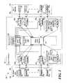
- FIG. 1is a block diagram of a data storage system according to the invention.
- FIG. 2is a block diagram of a portion of a system interface used in the data storage system of FIG. 1 ;
- FIG. 3is a diagram of an exemplary global cache memory printed circuit board used in the system interface of FIG. 1 ;
- FIG. 4is a block diagram of a pair of memory control/data sections on the exemplary global memory printed circuit board of FIG. 3 , such pair of memory control/data sections being coupled to a corresponding one of a plurality of memory array regions on the memory printed circuit board of FIG. 3 ;
- FIG. 5is a block diagram of an exemplary one of a pair of data logic sections used in one of the pair of memory control/data section of FIG. 4 ;
- FIG. 6is a block diagrams of an exemplary read-modify-write unit, here an arithmetic unit, used in the data logic section of FIG. 5 .
- the system interface 160includes: a plurality of, here 32 front-end directors (sometimes referred to as processors or controllers) 180 1 – 180 32 coupled to the host computer/server 120 via ports 123 1 – 123 32 ; a plurality of back-end directors 200 1 – 200 32 coupled to the bank of disk drives 140 via ports 123 33 – 123 64 ; a data transfer section 240 , having a global cache memory 220 , coupled to the plurality of front-end directors 180 1 – 180 16 and the back-end directors 200 1 – 200 16 ; and a messaging network 260 , operative independently of the data transfer section 240 , coupled to the plurality of front-end directors 180 1 – 180 32 and the plurality of back-end directors 200 1 – 200 32 , as shown.
- a data transfer section 240having a global cache memory 220 , coupled to the plurality of front-end directors 180 1 – 180 16 and the back-end directors 200 1 – 200 16 ; and a messaging network 260
- the front-end and back-end directors 180 1 – 180 32 , 200 1 – 200 32are functionally similar and include a microprocessor ( ⁇ P) 299 (i.e., a central processing unit (CPU) and RAM), a message engine/CPU controller 314 and a data pipe 316 , described in detail in the co-pending patent applications referred to above. Suffice it to say here, however, that the front-end and back-end directors 180 1 – 180 32 , 200 1 – 200 32 control data transfer between the host computer/server 120 and the bank of disk drives 140 in response to messages passing between the directors 180 1 – 180 32 , 200 1 – 200 32 through the messaging network 260 .
- ⁇ Pmicroprocessor
- the messagesfacilitate the data transfer between host computer/server 120 and the bank of disk drives 140 with such data passing through the global cache memory 220 via the data transfer section 240 . More particularly, in the case of the front-end directors 180 1 – 180 32 , the data passes between the host computer to the global cache memory 220 through the data pipe 316 in the front-end directors 180 1 – 180 32 and the messages pass through the message engine/CPU controller 314 in such front-end directors 180 1 – 180 32 .
- the datapasses between the back-end directors 200 1 – 200 32 and the bank of disk drives 140 and the global cache memory 220 through the data pipe 316 in the back-end directors 200 1 – 200 32 and again the messages pass through the message engine/CPU controller 314 in such back-end director 200 1 – 200 32 .
- each one of the director boards 190 1 – 210 8includes, as noted above four of the directors 180 1 – 180 32 , 200 1 – 200 32 ( FIG. 1 ).
- director boards 190 1 – 190 8 having four front-end directors per board, 180 1 – 180 32are referred to as front-end directors and the director boards 210 1 – 210 8 having four back-end directors per board, 200 1 – 200 32 are referred to as back-end directors.
- Each one of the directors 180 1 – 180 32 , 200 1 – 200 32includes the microprocessor 299 (referred to above), the message engine/CPU controller 314 , and the data pipe 316 shown in FIG. 1 .
- the front-end director boardshave ports 123 1 – 123 32 , as shown in FIG. 1 , coupled to the processors 121 1 – 121 32 , as shown.
- the back-end director boardshave ports 123 33 – 123 64 , as shown in FIG. 1 , coupled to the disk drives 141 1 – 141 32 , as shown.
- Each one of the director boards 190 1 – 190 8 and 210 1 – 210 8includes a crossbar switch 318 having a pair of crossbar switches 406 X, 406 Y.
- Each one of the switches 406 X, 406 Yincludes four input/output director-side ports C 1 –C 4 and the four input/output memory-side ports collectively designated in FIG. 2 by numerical designation 321 .
- the director-side ports C 1 –C 4 of switch 406 Xare connected to the four directors on the director board, as indicated, and as described in more detail in the co-pending patent applications referred to above.
- director-side ports C 1 –C 4 of switch 406 Yare also connected to the dual-ported directors on such board, as indicated.
- each directoris a dual-ported directors.
- Each one of the ports C 1 –C 4may be coupled to a selected one of the four ports collectively designated by 321 in accordance with control words provided to the switch 406 X by the directors on such board, respectively, as described in the above-referenced patent application. Suffice it to say here, that port 402 A of any one of the directors 180 1 , 180 3 , 180 5 , 180 7 may be coupled to any one of the ports 321 of switch 406 X, selectively in accordance with the control words. Likewise for switch 406 Y. Further details described in the co-pending patent applications referred to above.
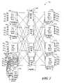
- the global cache memory 220includes a plurality of, here eight, cache memory boards M 0 –M 7 , as shown. Still further, referring to FIG. 3 , an exemplary one of the cache memory boards, here memory board M 0 , is shown. Here, each cache memory board includes four memory array regions 1 – 4 , an exemplary one thereof being shown and described in connection with FIG. 3 .
- each one of the memory boards M 0 –M 7has sixteen ports P. Each one of the sixteen ports P is connected to a corresponding one of the sixteen director boards 190 1 – 190 8 and 210 1 – 210 8 . Each one of the sixteen director boards 190 1 – 190 8 and 210 1 – 210 8 is able to couple one of the four directors thereon to any one of the eight memory boards M 0 –M 7 . For example, any one of the four directors on board 190 8 may be coupled to any one of the four memory boards M 0 –M 7 through the switches 406 X and 406 Y.
- each one of the directors on each one of the director bardsmay be selectively coupled to each one of the memory boards, and more particularly, to each one of the memory array regions 1 – 4 in the cache memory 220 .
- each one of the array regions 1 – 4may receive data from, or send data to, any one of the sixty-four directors.
- the exemplary memory boardincludes a plurality of, here four RAM memory array regions 1 – 4 , each one of the array regions has a pair of redundant data/control logic section, i.e., an A port logic section and a B port logic section, for receiving data to, or from, the memory array region as well as for receiving memory control signals.
- the memory boarditself has, as noted above in connection with FIG. 2 , sixteen ports P; a set of eight domain A ports P, here designated as ports P 0 –P 7 and a set of eight domain B ports P, here designated as ports P 8 –P 15 .
- each memory boardhas four logic networks (here crossbar switches). These four logic networks 221 1A , 221 2A , 221 1B , 221 2B , are here cross bar switches. Logic networks 221 1A , 221 2A , and logic networks 221 1B , 221 2B , are in two independent domains, i.e., domain A and domain B. Thus, logic networks 221 1A , 221 2A , are in domain A and logic networks 221 1B , 221 2B are in domain B, respectively.
- logic network 221 1Bis adapted to couple any one the ports P, thus here any one of the ports P 8 , P 9 , P 10 and P 11 to any one of the four ports Q 8 –Q 11 of such logic network 221 1B .
- logic network 221 2Bis adapted to couple any one the ports P, thus here any one of the ports P 12 , P 13 , P 14 and P 15 to any one of the four ports Q 12 –Q 15 of such logic network 221 ;
- logic network 221 1Ais adapted to couple any one the ports P, thus here any one of the ports P 0 , P 1 , P 2 and P 3 to any one of the four ports Q 0 –Q 3 of such logic network;
- logic network 221 2Ais adapted to couple any one the ports P, thus here any one of the ports P 4 , P 5 , P 6 and P 7 to any one of the four ports Q 4 –Q 7 of such logic network.
- each one of the memory printed circuit boardsis a set of four domain B memory control/data sections 300 1 – 300 4 and a set of four domain A memory control/data sections 302 1 – 302 4 .
- the memory board M 0includes four memory array regions 1 – 4 . Each memory array region has a DATA input coupled to both domain B memory control/data section 300 1 and domain a memory control/data section 300 2 . Further, each one of the domain B and domain A memory control/data sections 300 1 , 300 2 is coupled to a different pair of the logic networks 221 1B , 221 2B , 221 1A , and 221 2A .
- each one of the array regions 1 – 4may receive data from, or send data to, any one of the sixty-four directors.
- domain B memory control/data section 300 1is coupled to network 221 1B and 221 2B while domain A memory control/data section 300 2 is coupled to network 221 1A and 221 2A .
- memory control/data sections 300 1 , 300 2are shown in more detail and coupled to the memory array 1 .
- the memory control/data sections 300 1 , 300 2each includes a pair of control sections 400 , 402 ; a pair of data logic sections 404 , 406 ; and an arbiter 408 .
- the control section 400 and the data logic section 404 of memory control/data section 300 1are coupled to port Q 8 ( FIG. 3 ) and the control section 402 and the data logic section 406 of memory control/data section 300 1 are coupled to port Q 12 ( FIG. 3 ).
- the control section 400 and the data logic section 404 of memory control/data section 300 2are coupled to port Q 0 ( FIG.
- the memory array section 1has the DATA port 308 thereof coupled the data logic sections 404 , 406 in both memory control/data sections 300 1 and 300 2 , as shown.
- Memory address and control signalsare fed to the memory array region 1 by the control section 400 , 402 being granted access to the memory array region 1 by arbitration on for the memory array. Arbitration for access to the memory array region 1 is granted by arbitration is performed between arbiter 408 of memory control/data section 300 1 , and arbiter 408 of memory control/data section 300 2 .
- arbiter 408 of memory control/data section 300 1grants access of the memory array region 1 to data logic section 404 of memory control/data section 300 1 , one of the sixteen directors coupled to port Q 8 provides data to be written into, or requests data stored in, a selected address provided by such director. Further, such director may request a read-modify-write operation. More particularly, the director may request an atomic read-modify-write operation on plural bit read data stored in a selected one of a plurality of memory locations of region 1 , for example.
- each one of the memory locations, i.e., addresses, of the memory array region 1is here, for example, adapted to store data having sixty-four bits, here designated as bits C 63 –C 0 , C 0 is the least significant, or lowest order, bit and where C 63 is the most significant, or highest order, bit.
- the directorrequest that input data it provides to the memory be added to the data stored at an address provided by the director, (i.e., read data) and the result, i.e., the sum, or modified data, be written into the memory array region 1 at the same address from which the read data was stored.
- the director operationrequires that the read data (i.e., the data which was read from the memory prior to modification) be returned, unmodified, to the director. Also, this operation must be performed atomically. That is, no other director can have access to the selected address location in memory array region 1 until the modified data is written into such memory location.
- any portion (i.e., the entire portion or a fractional portion) of the read data in memorybe modified by a corresponding portion of the input data supplied by the director.
- the controllermay require that the entire sixty-four bit read word (i.e., C 63 –C 0 ) from memory array 1 be added to the entire sixty-four bit input word (A 63 –A 0 ,) supplied by the director and the sum of these two sixty-four bits words be written into memory array region 1 .
- the directormay require that only bits C 3 –C 0 be added to only bits A 3 –A 0 with the sum being stored in the locations previously occupied by bits C 3 –C 0 .
- the directormay require that bits C 19 –C 4 be added to bits A 19 –A 4 with the sum being stored in the locations previously occupied by bits C 19 –C 4 and simultaneously that bits C 63 –C 20 be added to bits A 63 –A 20 with the sum being stored in the locations previously occupied by bits C 63 –C 20 .
- Such operationsare performed in the data logic sections 404 , 406 in a manner to be described.
- the portion of the read data in memory be modified by a corresponding portion of the input data supplied by the directoris provided to the data logic section by a carry bit mask D 62 –D 0 provided by the requesting director.
- Such modification operationsare performed in the data logic sections 404 , 406 in a manner to be described.
- the arrangementenables a director to perform an atomic read-modify-write operation on plural bit read data stored in a selected one of a plurality of memory locations.
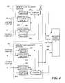
- FIG. 5An exemplary one of the data logic sections 404 , 406 , here data logic section 404 is shown in FIG. 5 to include: a write buffer 500 ; a read buffer 502 ; and, a read-modify-write unit 504 , here an arithmetic logic unit.
- the portion of the read data in memory be modified by a corresponding portion of the input data supplied by the directoris provided to the data logic section by a bits D 62 –D 0 of the carry bit mask provided by the requesting director. It is first noted that, for reasons to become apparent, that there is one less bit in the carry bit mask than the number of bits in the word stored in the memory array region 1 that is to be modified, thus, there are only 63 bits in the carry bit mask in the examples being described. Thus, referring to FIG.
- the directorprovides on port Q 8 the input data (A 63 –A 0 ) and the bits (D 62 –D 0 ) of the carry bit mask, it being understood that the address location in the memory array region 1 at port Q 8 is fed to control section 400 ( FIG. 4 ).
- the input data (A 63 –A 0 ) and the carry bit maski.e., the logic state of bits D 62 –D 0
- the write buffer 500and that they are combined into a parallel, 127-bit digital word having both the input data (A 63 –A 0 ) and the bits (D 62 –D 0 ) of a carry bit mask.
- the data at the location specified by the directori.e., the unmodified read data (C 63 –C 0 ) is, in response to the read-modify-write request by the controller, retrieved from the memory array region 1 at the director specified address and is: (1) fed back to the requesting director; and (2) is fed to the read-modify-write section 504 .
- the unmodified read data (C 63 –C 0 ) in read buffer 502 and the 127-bit digital word having both the input data (A 63 –A 0 ) and the bits (D 62 –D 0 ) of a carry bit mask in write buffer 500are fed to the read-modify-write unit 504 , here an arithmetic logic unit.
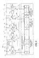
- the read-modify-write unit 504is shown in FIG. 6 to include a plurality of full adder sections 600 0 – 600 63 .
- One of the full adder sections 600 0 – 600 63is provided for each one of the bits of the read data (C 63 –C 0 ), respectively as indicated.
- Each one of the full adder sections 600 0 – 600 63has a carry bit input CI and a carry bit output CO, except for section 600 63 which only has a carry bit input CI.
- the read-modify-write unit 504includes a plurality, here sixty-two, logic gates 602 0 – 602 62 .
- the logic gatesare AND gates having a pair of inputs.
- One of the inputsis an inverting input and is coupled to a corresponding one of the bits D 0 –D 62 of a carry bit mask, respectively as indicated.
- the other one of the inputsis coupled to the carry bit output CO of a preceding full adder section.
- the other input of gates 602 0 – 602 62are coupled to the carry bit output CO of full adder section 600 0 – 600 62 (not shown but immediately preceding adder 600 63 ), respectively, as indicated.
- Each one of the full adders 600 0 – 600 63produces a summation output 606 0 – 606 63 , respectively having the least significant bit produced by the adder.
- the summation outputthus has the modified data indicated as C′ 63 –C′ 0 .
- the modified data C′ 63 –C′ 0is then written back into the memory region 1 at the same location from which unmodified data C 63 –C 0 was read.
- each one of the full adders 600 0 – 600 63produces the least significant bit of the sum of the two bits fed thereto from the input data supplied by the director and the read data from the memory array region on a corresponding one of the summation outputs 606 0 – 606 63 which is then fed to the memory array region 1 and the bit on the carry bit input (CI) fed to such adder.
- the adderalso produces a carry output on its carry bit output (CO) representative of the most significant bit produced by the full adder, it being noted that the carry out bit may be either a logic 0 or logic 1 depending on the logic states fed to such full adder.
- bits C′ 63 –C′ 0 produced on the summation outputs 606 0 – 606 63 , respectively, by full adders 600 63 – 600 0 , respectively,are fed for storage in memory array region 1 at the address specified by the director to effect the atomic, read-modify-write operation.
- carry bit on the carry bit input of full adder 600 0is fixed at logic 0 and that the last adder 600 63 does not have a carry bit output CO.
- full adder 600 3produces a carry bit or logic 1, such carry bit will not pass through gate 602 4 to the carry bit input (CI) of full adder 600 4 if bit D 4 of the carry bit mask is logic 1 but such carry bit will pass through gate 602 4 to the carry bit input (CI) of full adder 600 4 if D 4 of the carry bit mask is logic 0.
- the arrangementoperates by adding each one of a bits of plural bit input data provided by the director with a corresponding one of the bits of the plural bit read data in the provided full adder together with a carry bit fed the carry bit input of such provided full adder.
- the full adderprovides: a carry bit; and, a summation of the bits fed to such provided full adder to the corresponding bit location in the selected one of a plurality of memory locations.
- the systemselectively couples, or inhibits coupling, a carry bit produced by one full adder provided for a lower order bit of the plural bit read data to the carry bit input of a second full adder provided by for next, successive higher order bit of the plural bit read data selectively in accordance with a bit of the carry bit mask provided by the director.
- each one of the full addersis associated with a corresponding one of the bits of the plural bit read data.
- Each one of the full addershas a summation output, a carry bit input and a carry bit output.
- the methodincludes adding in each one of the full adders: (a) a corresponding bit of plural bit input data provided by the director; (b) the corresponding one of the bits of the plural bit read data; and, (c) a carry bit fed the carry bit input from a preceding full adder.
- Each one of the full addersprovides: (a) a carry bit on the carry output thereof representative of the most significant bit produced by the full adder; and, (b) a bit on the summation output representative of a least significant bit produced by the full adder.
- the bit on the summation outputis stored in a corresponding bit location in the selected one of a plurality of memory locations.
- the methodselectively couples, or inhibits coupling, the carry bit produced from one of the full adders to the carry bit input of a next successive full adder selectively in accordance with a corresponding bit of a plural bit carry bit mask provided by the director.
- the summationmay be performed on read data of arbitrary length and position in the selected memory location. Also, multiple portions of the read data may be simultaneously added to corresponding multiple portions of the input data provided by the director.
- the bits of a carry bit mask provided by the directorcontrol whether the carry bit will be forward, (i.e., carry bit of the preceding order adder), will pass as to the carry bit input of the next higher order adder.
- inhibiting coupling of an carry bitestablishes a boundary between the most significant bit of a lower order portion of the read data and the least significant bit of the next higher order portion of such read data. Coupling all carry bits enables the entire read data to be added to the entire input data.
Landscapes
- Engineering & Computer Science (AREA)
- Software Systems (AREA)
- Theoretical Computer Science (AREA)
- Physics & Mathematics (AREA)
- General Physics & Mathematics (AREA)
- General Engineering & Computer Science (AREA)
- Computational Mathematics (AREA)
- Mathematical Analysis (AREA)
- Mathematical Optimization (AREA)
- Pure & Applied Mathematics (AREA)
- Memory System (AREA)
Abstract
Description
| FILING | Ser. | ||
| INVENTORS | DATE | No. | TITLE |
| Yuval Ofek et al. | Mar. 31, 2000 | 09/540,828 | Data Storage System |
| Having Separate Data | |||
| Transfer Section And | |||
| Message Network | |||
| Paul C. Wilson et | Jun. 29, 2000 | 09/606,730 | Data Storage System |
| al. | Having Point-To-Point | ||
| Configuration | |||
| John K. Walton et | Jan. 22, 2002 | 10/054,241 | Data Storage System |
| al. | (Divisional of | ||
| 09/223,519 filed | |||
| Dec. 30, 1998) | |||
| Christopher S. | Dec. 21, 2000 | 09/745,859 | Data Storage System |
| MacLellan et al. | Having Plural Fault | ||
| Domains | |||
| John K. Walton | May 17, 2001 | 09/859,659 | Data Storage System |
| Having No-Operation | |||
| Command | |||
Claims (6)
Priority Applications (1)
| Application Number | Priority Date | Filing Date | Title |
|---|---|---|---|
| US10/331,366US6973551B1 (en) | 2002-12-30 | 2002-12-30 | Data storage system having atomic memory operation |
Applications Claiming Priority (1)
| Application Number | Priority Date | Filing Date | Title |
|---|---|---|---|
| US10/331,366US6973551B1 (en) | 2002-12-30 | 2002-12-30 | Data storage system having atomic memory operation |
Publications (1)
| Publication Number | Publication Date |
|---|---|
| US6973551B1true US6973551B1 (en) | 2005-12-06 |
Family
ID=35430630
Family Applications (1)
| Application Number | Title | Priority Date | Filing Date |
|---|---|---|---|
| US10/331,366Expired - LifetimeUS6973551B1 (en) | 2002-12-30 | 2002-12-30 | Data storage system having atomic memory operation |
Country Status (1)
| Country | Link |
|---|---|
| US (1) | US6973551B1 (en) |
Cited By (30)
| Publication number | Priority date | Publication date | Assignee | Title |
|---|---|---|---|---|
| US20060090044A1 (en)* | 2004-10-21 | 2006-04-27 | International Business Machines Corporation | Memory controller and method for optimized read/modify/write performance |
| US20060107003A1 (en)* | 2004-11-12 | 2006-05-18 | International Business Machines Corporation | Separate handling of read and write of read-modify-write |
| US20080040414A1 (en)* | 2006-08-09 | 2008-02-14 | Infineon Technologies Ag | Standard cell for arithmetic logic unit and chip card controller |
| US7707367B1 (en)* | 2007-06-28 | 2010-04-27 | Emc Corporation | Data storage system having separate atomic operation/non-atomic operation paths |
| US20100332769A1 (en)* | 2009-06-25 | 2010-12-30 | International Business Machines Corporation | Updating Shared Variables Atomically |
| US7979588B1 (en)* | 2007-06-28 | 2011-07-12 | Emc Corporation | Data storage system having acceleration path for congested packet switching network |
| US7979572B1 (en) | 2007-06-28 | 2011-07-12 | Emc Corporation | Data storage system having operation code in address portion for atomic operations |
| US7987229B1 (en) | 2007-06-28 | 2011-07-26 | Emc Corporation | Data storage system having plural data pipes |
| US8090789B1 (en) | 2007-06-28 | 2012-01-03 | Emc Corporation | Method of operating a data storage system having plural data pipes |
| WO2012016089A3 (en)* | 2010-07-28 | 2012-05-31 | Fusion-Io, Inc. | Apparatus, system, and method for conditional and atomic storage operations |
| US20120163585A1 (en)* | 2010-12-22 | 2012-06-28 | Electronics And Telecommunications Research Instittute | Masking addition operation device for prevention of side channel attack |
| US20130091330A1 (en)* | 2010-05-18 | 2013-04-11 | Lsi Corporation | Early Cache Eviction in a Multi-Flow Network Processor Architecture |
| US8725934B2 (en) | 2011-12-22 | 2014-05-13 | Fusion-Io, Inc. | Methods and appratuses for atomic storage operations |
| US8984216B2 (en) | 2010-09-09 | 2015-03-17 | Fusion-Io, Llc | Apparatus, system, and method for managing lifetime of a storage device |
| US9015425B2 (en) | 2009-09-09 | 2015-04-21 | Intelligent Intellectual Property Holdings 2, LLC. | Apparatus, systems, and methods for nameless writes |
| US9218278B2 (en) | 2010-12-13 | 2015-12-22 | SanDisk Technologies, Inc. | Auto-commit memory |
| US9223514B2 (en) | 2009-09-09 | 2015-12-29 | SanDisk Technologies, Inc. | Erase suspend/resume for memory |
| US9251086B2 (en) | 2012-01-24 | 2016-02-02 | SanDisk Technologies, Inc. | Apparatus, system, and method for managing a cache |
| US9274937B2 (en) | 2011-12-22 | 2016-03-01 | Longitude Enterprise Flash S.A.R.L. | Systems, methods, and interfaces for vector input/output operations |
| US9305610B2 (en) | 2009-09-09 | 2016-04-05 | SanDisk Technologies, Inc. | Apparatus, system, and method for power reduction management in a storage device |
| WO2016097676A1 (en)* | 2014-12-19 | 2016-06-23 | Arm Limited | Atomic add with carry instruction |
| US9658953B2 (en) | 2009-08-20 | 2017-05-23 | Rambus Inc. | Single command, multiple column-operation memory device |
| US20170235557A1 (en)* | 2016-02-16 | 2017-08-17 | Microsoft Technology Licensing, Llc. | Translating atomic read-modify-write accesses |
| US9767017B2 (en) | 2010-12-13 | 2017-09-19 | Sandisk Technologies Llc | Memory device with volatile and non-volatile media |
| US10133662B2 (en) | 2012-06-29 | 2018-11-20 | Sandisk Technologies Llc | Systems, methods, and interfaces for managing persistent data of atomic storage operations |
| US10817421B2 (en) | 2010-12-13 | 2020-10-27 | Sandisk Technologies Llc | Persistent data structures |
| US10817502B2 (en) | 2010-12-13 | 2020-10-27 | Sandisk Technologies Llc | Persistent memory management |
| US11573909B2 (en) | 2006-12-06 | 2023-02-07 | Unification Technologies Llc | Apparatus, system, and method for managing commands of solid-state storage using bank interleave |
| CN115910153A (en)* | 2021-08-11 | 2023-04-04 | 意法半导体国际有限公司 | Static random access memory supporting single clock cycle read-modify-write operation |
| US20240170032A1 (en)* | 2022-11-17 | 2024-05-23 | Stmicroelectronics International N.V. | Static random access memory supporting a dynamically variable duration self-time delay for a single clock cycle read-modify-write operation |
Citations (3)
| Publication number | Priority date | Publication date | Assignee | Title |
|---|---|---|---|---|
| US4075704A (en)* | 1976-07-02 | 1978-02-21 | Floating Point Systems, Inc. | Floating point data processor for high speech operation |
| US5668967A (en)* | 1993-10-12 | 1997-09-16 | Wang Laboratories, Inc. | Apparatus and methods for reducing numbers of read-modify-write cycles to a memory, and for improving DMA efficiency |
| US5752273A (en)* | 1995-05-26 | 1998-05-12 | National Semiconductor Corporation | Apparatus and method for efficiently determining addresses for misaligned data stored in memory |
- 2002
- 2002-12-30USUS10/331,366patent/US6973551B1/ennot_activeExpired - Lifetime
Patent Citations (3)
| Publication number | Priority date | Publication date | Assignee | Title |
|---|---|---|---|---|
| US4075704A (en)* | 1976-07-02 | 1978-02-21 | Floating Point Systems, Inc. | Floating point data processor for high speech operation |
| US5668967A (en)* | 1993-10-12 | 1997-09-16 | Wang Laboratories, Inc. | Apparatus and methods for reducing numbers of read-modify-write cycles to a memory, and for improving DMA efficiency |
| US5752273A (en)* | 1995-05-26 | 1998-05-12 | National Semiconductor Corporation | Apparatus and method for efficiently determining addresses for misaligned data stored in memory |
Non-Patent Citations (1)
| Title |
|---|
| Ting-Lu Huang, Dec. 14-16, 1998, IEEE, Pges: 292-299.* |
Cited By (66)
| Publication number | Priority date | Publication date | Assignee | Title |
|---|---|---|---|---|
| US7475202B2 (en)* | 2004-10-21 | 2009-01-06 | International Business Machines Corporation | Memory controller and method for optimized read/modify/write performance |
| US20060090044A1 (en)* | 2004-10-21 | 2006-04-27 | International Business Machines Corporation | Memory controller and method for optimized read/modify/write performance |
| US20080016294A1 (en)* | 2004-10-21 | 2008-01-17 | International Business Machines Corporation | Memory controller and method for optimized read/modify/write performance |
| US7328317B2 (en)* | 2004-10-21 | 2008-02-05 | International Business Machines Corporation | Memory controller and method for optimized read/modify/write performance |
| US7908443B2 (en) | 2004-10-21 | 2011-03-15 | International Business Machines Corporation | Memory controller and method for optimized read/modify/write performance |
| US20090024808A1 (en)* | 2004-10-21 | 2009-01-22 | International Business Machines Corporation | Memory controller and method for optimized read/modify/write performance |
| US20090024807A1 (en)* | 2004-10-21 | 2009-01-22 | International Business Machines Corporation | Memory controller and method for optimized read/modify/write performance |
| US7363442B2 (en)* | 2004-11-12 | 2008-04-22 | International Business Machines Corporation | Separate handling of read and write of read-modify-write |
| US7716430B2 (en) | 2004-11-12 | 2010-05-11 | International Business Machines Corporation | Separate handling of read and write of read-modify-write |
| US20080147969A1 (en)* | 2004-11-12 | 2008-06-19 | Melissa Ann Barnum | Separate Handling of Read and Write of Read-Modify-Write |
| US20060107003A1 (en)* | 2004-11-12 | 2006-05-18 | International Business Machines Corporation | Separate handling of read and write of read-modify-write |
| US20080148108A1 (en)* | 2004-11-12 | 2008-06-19 | Barnum Melissa A | Separate Handling of Read and Write of Read-Modify-Write |
| US7676639B2 (en) | 2004-11-12 | 2010-03-09 | International Business Machines Corporation | Separate handling of read and write of read-modify-write |
| US8135767B2 (en) | 2006-08-09 | 2012-03-13 | Thomas Kuenemund | Standard cell for arithmetic logic unit and chip card controller |
| DE102007037363B4 (en)* | 2006-08-09 | 2016-09-22 | Infineon Technologies Ag | Standard cell for arithmetic logic unit and smart card control |
| US20080040414A1 (en)* | 2006-08-09 | 2008-02-14 | Infineon Technologies Ag | Standard cell for arithmetic logic unit and chip card controller |
| US7921148B2 (en)* | 2006-08-09 | 2011-04-05 | Infineon Technologies Ag | Standard cell for arithmetic logic unit and chip card controller |
| US20080126456A1 (en)* | 2006-08-09 | 2008-05-29 | Infineon Technologies Ag | Standard cell for arithmetic logic unit and chip card controller |
| US11573909B2 (en) | 2006-12-06 | 2023-02-07 | Unification Technologies Llc | Apparatus, system, and method for managing commands of solid-state storage using bank interleave |
| US11640359B2 (en) | 2006-12-06 | 2023-05-02 | Unification Technologies Llc | Systems and methods for identifying storage resources that are not in use |
| US11847066B2 (en) | 2006-12-06 | 2023-12-19 | Unification Technologies Llc | Apparatus, system, and method for managing commands of solid-state storage using bank interleave |
| US11960412B2 (en) | 2006-12-06 | 2024-04-16 | Unification Technologies Llc | Systems and methods for identifying storage resources that are not in use |
| US7987229B1 (en) | 2007-06-28 | 2011-07-26 | Emc Corporation | Data storage system having plural data pipes |
| US7979572B1 (en) | 2007-06-28 | 2011-07-12 | Emc Corporation | Data storage system having operation code in address portion for atomic operations |
| US8090789B1 (en) | 2007-06-28 | 2012-01-03 | Emc Corporation | Method of operating a data storage system having plural data pipes |
| US7707367B1 (en)* | 2007-06-28 | 2010-04-27 | Emc Corporation | Data storage system having separate atomic operation/non-atomic operation paths |
| US7979588B1 (en)* | 2007-06-28 | 2011-07-12 | Emc Corporation | Data storage system having acceleration path for congested packet switching network |
| US8495311B2 (en)* | 2009-06-25 | 2013-07-23 | International Business Machines Corporation | Updating shared variables atomically |
| US20100332769A1 (en)* | 2009-06-25 | 2010-12-30 | International Business Machines Corporation | Updating Shared Variables Atomically |
| US11748252B2 (en) | 2009-08-20 | 2023-09-05 | Rambus Inc. | Data write from pre-programmed register |
| US11720485B2 (en) | 2009-08-20 | 2023-08-08 | Rambus Inc. | DRAM with command-differentiated storage of internally and externally sourced data |
| US12189523B2 (en) | 2009-08-20 | 2025-01-07 | Rambus Inc. | Command-differentiated storage of internally and externally sourced data |
| US11204863B2 (en) | 2009-08-20 | 2021-12-21 | Rambus Inc. | Memory component that performs data write from pre-programmed register |
| US10552310B2 (en) | 2009-08-20 | 2020-02-04 | Rambus Inc. | Single command, multiple column-operation memory device |
| US9898400B2 (en) | 2009-08-20 | 2018-02-20 | Rambus Inc. | Single command, multiple column-operation memory device |
| US9658953B2 (en) | 2009-08-20 | 2017-05-23 | Rambus Inc. | Single command, multiple column-operation memory device |
| US9015425B2 (en) | 2009-09-09 | 2015-04-21 | Intelligent Intellectual Property Holdings 2, LLC. | Apparatus, systems, and methods for nameless writes |
| US9223514B2 (en) | 2009-09-09 | 2015-12-29 | SanDisk Technologies, Inc. | Erase suspend/resume for memory |
| US9251062B2 (en) | 2009-09-09 | 2016-02-02 | Intelligent Intellectual Property Holdings 2 Llc | Apparatus, system, and method for conditional and atomic storage operations |
| US9305610B2 (en) | 2009-09-09 | 2016-04-05 | SanDisk Technologies, Inc. | Apparatus, system, and method for power reduction management in a storage device |
| US9152564B2 (en)* | 2010-05-18 | 2015-10-06 | Intel Corporation | Early cache eviction in a multi-flow network processor architecture |
| US20130091330A1 (en)* | 2010-05-18 | 2013-04-11 | Lsi Corporation | Early Cache Eviction in a Multi-Flow Network Processor Architecture |
| US9910777B2 (en) | 2010-07-28 | 2018-03-06 | Sandisk Technologies Llc | Enhanced integrity through atomic writes in cache |
| WO2012016089A3 (en)* | 2010-07-28 | 2012-05-31 | Fusion-Io, Inc. | Apparatus, system, and method for conditional and atomic storage operations |
| US10013354B2 (en) | 2010-07-28 | 2018-07-03 | Sandisk Technologies Llc | Apparatus, system, and method for atomic storage operations |
| US8984216B2 (en) | 2010-09-09 | 2015-03-17 | Fusion-Io, Llc | Apparatus, system, and method for managing lifetime of a storage device |
| US10817502B2 (en) | 2010-12-13 | 2020-10-27 | Sandisk Technologies Llc | Persistent memory management |
| US9218278B2 (en) | 2010-12-13 | 2015-12-22 | SanDisk Technologies, Inc. | Auto-commit memory |
| US9767017B2 (en) | 2010-12-13 | 2017-09-19 | Sandisk Technologies Llc | Memory device with volatile and non-volatile media |
| US9772938B2 (en) | 2010-12-13 | 2017-09-26 | Sandisk Technologies Llc | Auto-commit memory metadata and resetting the metadata by writing to special address in free space of page storing the metadata |
| US10817421B2 (en) | 2010-12-13 | 2020-10-27 | Sandisk Technologies Llc | Persistent data structures |
| US20120163585A1 (en)* | 2010-12-22 | 2012-06-28 | Electronics And Telecommunications Research Instittute | Masking addition operation device for prevention of side channel attack |
| US8774406B2 (en)* | 2010-12-22 | 2014-07-08 | Electronics And Telecommunications Research Institute | Masking addition operation device for prevention of side channel attack |
| US9274937B2 (en) | 2011-12-22 | 2016-03-01 | Longitude Enterprise Flash S.A.R.L. | Systems, methods, and interfaces for vector input/output operations |
| US10296220B2 (en) | 2011-12-22 | 2019-05-21 | Sandisk Technologies Llc | Systems, methods, and interfaces for vector input/output operations |
| US8725934B2 (en) | 2011-12-22 | 2014-05-13 | Fusion-Io, Inc. | Methods and appratuses for atomic storage operations |
| US9251086B2 (en) | 2012-01-24 | 2016-02-02 | SanDisk Technologies, Inc. | Apparatus, system, and method for managing a cache |
| US10133662B2 (en) | 2012-06-29 | 2018-11-20 | Sandisk Technologies Llc | Systems, methods, and interfaces for managing persistent data of atomic storage operations |
| CN107003855B (en)* | 2014-12-19 | 2021-03-26 | Arm 有限公司 | Atomic addition instruction with carry |
| US11036500B2 (en) | 2014-12-19 | 2021-06-15 | Arm Limited | Technique for processing a sequence of atomic add with carry instructions when a data value is not present in a cache |
| CN107003855A (en)* | 2014-12-19 | 2017-08-01 | Arm 有限公司 | Atom addition instruction with carry |
| WO2016097676A1 (en)* | 2014-12-19 | 2016-06-23 | Arm Limited | Atomic add with carry instruction |
| US9996329B2 (en)* | 2016-02-16 | 2018-06-12 | Microsoft Technology Licensing, Llc | Translating atomic read-modify-write accesses |
| US20170235557A1 (en)* | 2016-02-16 | 2017-08-17 | Microsoft Technology Licensing, Llc. | Translating atomic read-modify-write accesses |
| CN115910153A (en)* | 2021-08-11 | 2023-04-04 | 意法半导体国际有限公司 | Static random access memory supporting single clock cycle read-modify-write operation |
| US20240170032A1 (en)* | 2022-11-17 | 2024-05-23 | Stmicroelectronics International N.V. | Static random access memory supporting a dynamically variable duration self-time delay for a single clock cycle read-modify-write operation |
Similar Documents
| Publication | Publication Date | Title |
|---|---|---|
| US6973551B1 (en) | Data storage system having atomic memory operation | |
| KR100585414B1 (en) | Data storage systems | |
| US7581060B2 (en) | Storage device control apparatus and control method for the storage device control apparatus | |
| EP1606712B1 (en) | System and method for dynamic mirror-bank addressing | |
| US5819310A (en) | Method and apparatus for reading data from mirrored logical volumes on physical disk drives | |
| US6961818B1 (en) | Method, system and computer program product for managing data in a mirrored cache using an access balancing technique | |
| JP2002510079A (en) | Method and apparatus for forcing ordered execution of reads and writes between memory interfaces | |
| JPS6284350A (en) | Hierarchical cash memory apparatus and method | |
| US11287988B2 (en) | Autonomous raid data storage device locking system | |
| US6877061B2 (en) | Data storage system having dummy printed circuit boards | |
| US6954825B2 (en) | Disk subsystem | |
| US7260575B2 (en) | Performance optimization for data sharing across batch sequential processes and on-line transaction processes | |
| US6950906B2 (en) | System for and method of operating a cache | |
| US20040193973A1 (en) | Data storage system | |
| US6397281B1 (en) | Bus arbitration system | |
| US7752340B1 (en) | Atomic command retry in a data storage system | |
| CN1215416C (en) | Read operations in multiprocessor computer systems | |
| JP3488190B2 (en) | Method and system for transferring data between devices on a bus | |
| US6249878B1 (en) | Data storage system | |
| US7313656B1 (en) | Pre-fetch prediction method for disk drives | |
| US6914784B1 (en) | Data storage system cabinet | |
| JP3206453B2 (en) | Shared file update control method | |
| US6907483B1 (en) | Data storage system having dummy printed circuit boards with jumpers | |
| WO2003083638A2 (en) | Data storage system | |
| US7099980B1 (en) | Data storage system having port disable mechanism |
Legal Events
| Date | Code | Title | Description |
|---|---|---|---|
| AS | Assignment | Owner name:EMC CORPORATION, MASSACHUSETTS Free format text:ASSIGNMENT OF ASSIGNORS INTEREST;ASSIGNOR:WALTON, JOHN K.;REEL/FRAME:013627/0920 Effective date:20021217 | |
| STCF | Information on status: patent grant | Free format text:PATENTED CASE | |
| FPAY | Fee payment | Year of fee payment:4 | |
| FPAY | Fee payment | Year of fee payment:8 | |
| AS | Assignment | Owner name:CREDIT SUISSE AG, CAYMAN ISLANDS BRANCH, AS COLLATERAL AGENT, NORTH CAROLINA Free format text:SECURITY AGREEMENT;ASSIGNORS:ASAP SOFTWARE EXPRESS, INC.;AVENTAIL LLC;CREDANT TECHNOLOGIES, INC.;AND OTHERS;REEL/FRAME:040134/0001 Effective date:20160907 Owner name:THE BANK OF NEW YORK MELLON TRUST COMPANY, N.A., AS NOTES COLLATERAL AGENT, TEXAS Free format text:SECURITY AGREEMENT;ASSIGNORS:ASAP SOFTWARE EXPRESS, INC.;AVENTAIL LLC;CREDANT TECHNOLOGIES, INC.;AND OTHERS;REEL/FRAME:040136/0001 Effective date:20160907 Owner name:CREDIT SUISSE AG, CAYMAN ISLANDS BRANCH, AS COLLAT Free format text:SECURITY AGREEMENT;ASSIGNORS:ASAP SOFTWARE EXPRESS, INC.;AVENTAIL LLC;CREDANT TECHNOLOGIES, INC.;AND OTHERS;REEL/FRAME:040134/0001 Effective date:20160907 Owner name:THE BANK OF NEW YORK MELLON TRUST COMPANY, N.A., A Free format text:SECURITY AGREEMENT;ASSIGNORS:ASAP SOFTWARE EXPRESS, INC.;AVENTAIL LLC;CREDANT TECHNOLOGIES, INC.;AND OTHERS;REEL/FRAME:040136/0001 Effective date:20160907 | |
| AS | Assignment | Owner name:EMC IP HOLDING COMPANY LLC, MASSACHUSETTS Free format text:ASSIGNMENT OF ASSIGNORS INTEREST;ASSIGNOR:EMC CORPORATION;REEL/FRAME:040203/0001 Effective date:20160906 | |
| FPAY | Fee payment | Year of fee payment:12 | |
| AS | Assignment | Owner name:THE BANK OF NEW YORK MELLON TRUST COMPANY, N.A., T Free format text:SECURITY AGREEMENT;ASSIGNORS:CREDANT TECHNOLOGIES, INC.;DELL INTERNATIONAL L.L.C.;DELL MARKETING L.P.;AND OTHERS;REEL/FRAME:049452/0223 Effective date:20190320 Owner name:THE BANK OF NEW YORK MELLON TRUST COMPANY, N.A., TEXAS Free format text:SECURITY AGREEMENT;ASSIGNORS:CREDANT TECHNOLOGIES, INC.;DELL INTERNATIONAL L.L.C.;DELL MARKETING L.P.;AND OTHERS;REEL/FRAME:049452/0223 Effective date:20190320 | |
| AS | Assignment | Owner name:THE BANK OF NEW YORK MELLON TRUST COMPANY, N.A., TEXAS Free format text:SECURITY AGREEMENT;ASSIGNORS:CREDANT TECHNOLOGIES INC.;DELL INTERNATIONAL L.L.C.;DELL MARKETING L.P.;AND OTHERS;REEL/FRAME:053546/0001 Effective date:20200409 | |
| AS | Assignment | Owner name:WYSE TECHNOLOGY L.L.C., CALIFORNIA Free format text:RELEASE BY SECURED PARTY;ASSIGNOR:CREDIT SUISSE AG, CAYMAN ISLANDS BRANCH;REEL/FRAME:058216/0001 Effective date:20211101 Owner name:SCALEIO LLC, MASSACHUSETTS Free format text:RELEASE BY SECURED PARTY;ASSIGNOR:CREDIT SUISSE AG, CAYMAN ISLANDS BRANCH;REEL/FRAME:058216/0001 Effective date:20211101 Owner name:MOZY, INC., WASHINGTON Free format text:RELEASE BY SECURED PARTY;ASSIGNOR:CREDIT SUISSE AG, CAYMAN ISLANDS BRANCH;REEL/FRAME:058216/0001 Effective date:20211101 Owner name:MAGINATICS LLC, CALIFORNIA Free format text:RELEASE BY SECURED PARTY;ASSIGNOR:CREDIT SUISSE AG, CAYMAN ISLANDS BRANCH;REEL/FRAME:058216/0001 Effective date:20211101 Owner name:FORCE10 NETWORKS, INC., CALIFORNIA Free format text:RELEASE BY SECURED PARTY;ASSIGNOR:CREDIT SUISSE AG, CAYMAN ISLANDS BRANCH;REEL/FRAME:058216/0001 Effective date:20211101 Owner name:EMC IP HOLDING COMPANY LLC, TEXAS Free format text:RELEASE BY SECURED PARTY;ASSIGNOR:CREDIT SUISSE AG, CAYMAN ISLANDS BRANCH;REEL/FRAME:058216/0001 Effective date:20211101 Owner name:EMC CORPORATION, MASSACHUSETTS Free format text:RELEASE BY SECURED PARTY;ASSIGNOR:CREDIT SUISSE AG, CAYMAN ISLANDS BRANCH;REEL/FRAME:058216/0001 Effective date:20211101 Owner name:DELL SYSTEMS CORPORATION, TEXAS Free format text:RELEASE BY SECURED PARTY;ASSIGNOR:CREDIT SUISSE AG, CAYMAN ISLANDS BRANCH;REEL/FRAME:058216/0001 Effective date:20211101 Owner name:DELL SOFTWARE INC., CALIFORNIA Free format text:RELEASE BY SECURED PARTY;ASSIGNOR:CREDIT SUISSE AG, CAYMAN ISLANDS BRANCH;REEL/FRAME:058216/0001 Effective date:20211101 Owner name:DELL PRODUCTS L.P., TEXAS Free format text:RELEASE BY SECURED PARTY;ASSIGNOR:CREDIT SUISSE AG, CAYMAN ISLANDS BRANCH;REEL/FRAME:058216/0001 Effective date:20211101 Owner name:DELL MARKETING L.P., TEXAS Free format text:RELEASE BY SECURED PARTY;ASSIGNOR:CREDIT SUISSE AG, CAYMAN ISLANDS BRANCH;REEL/FRAME:058216/0001 Effective date:20211101 Owner name:DELL INTERNATIONAL, L.L.C., TEXAS Free format text:RELEASE BY SECURED PARTY;ASSIGNOR:CREDIT SUISSE AG, CAYMAN ISLANDS BRANCH;REEL/FRAME:058216/0001 Effective date:20211101 Owner name:DELL USA L.P., TEXAS Free format text:RELEASE BY SECURED PARTY;ASSIGNOR:CREDIT SUISSE AG, CAYMAN ISLANDS BRANCH;REEL/FRAME:058216/0001 Effective date:20211101 Owner name:CREDANT TECHNOLOGIES, INC., TEXAS Free format text:RELEASE BY SECURED PARTY;ASSIGNOR:CREDIT SUISSE AG, CAYMAN ISLANDS BRANCH;REEL/FRAME:058216/0001 Effective date:20211101 Owner name:AVENTAIL LLC, CALIFORNIA Free format text:RELEASE BY SECURED PARTY;ASSIGNOR:CREDIT SUISSE AG, CAYMAN ISLANDS BRANCH;REEL/FRAME:058216/0001 Effective date:20211101 Owner name:ASAP SOFTWARE EXPRESS, INC., ILLINOIS Free format text:RELEASE BY SECURED PARTY;ASSIGNOR:CREDIT SUISSE AG, CAYMAN ISLANDS BRANCH;REEL/FRAME:058216/0001 Effective date:20211101 | |
| AS | Assignment | Owner name:SCALEIO LLC, MASSACHUSETTS Free format text:RELEASE OF SECURITY INTEREST IN PATENTS PREVIOUSLY RECORDED AT REEL/FRAME (040136/0001);ASSIGNOR:THE BANK OF NEW YORK MELLON TRUST COMPANY, N.A., AS NOTES COLLATERAL AGENT;REEL/FRAME:061324/0001 Effective date:20220329 Owner name:EMC IP HOLDING COMPANY LLC (ON BEHALF OF ITSELF AND AS SUCCESSOR-IN-INTEREST TO MOZY, INC.), TEXAS Free format text:RELEASE OF SECURITY INTEREST IN PATENTS PREVIOUSLY RECORDED AT REEL/FRAME (040136/0001);ASSIGNOR:THE BANK OF NEW YORK MELLON TRUST COMPANY, N.A., AS NOTES COLLATERAL AGENT;REEL/FRAME:061324/0001 Effective date:20220329 Owner name:EMC CORPORATION (ON BEHALF OF ITSELF AND AS SUCCESSOR-IN-INTEREST TO MAGINATICS LLC), MASSACHUSETTS Free format text:RELEASE OF SECURITY INTEREST IN PATENTS PREVIOUSLY RECORDED AT REEL/FRAME (040136/0001);ASSIGNOR:THE BANK OF NEW YORK MELLON TRUST COMPANY, N.A., AS NOTES COLLATERAL AGENT;REEL/FRAME:061324/0001 Effective date:20220329 Owner name:DELL MARKETING CORPORATION (SUCCESSOR-IN-INTEREST TO FORCE10 NETWORKS, INC. AND WYSE TECHNOLOGY L.L.C.), TEXAS Free format text:RELEASE OF SECURITY INTEREST IN PATENTS PREVIOUSLY RECORDED AT REEL/FRAME (040136/0001);ASSIGNOR:THE BANK OF NEW YORK MELLON TRUST COMPANY, N.A., AS NOTES COLLATERAL AGENT;REEL/FRAME:061324/0001 Effective date:20220329 Owner name:DELL PRODUCTS L.P., TEXAS Free format text:RELEASE OF SECURITY INTEREST IN PATENTS PREVIOUSLY RECORDED AT REEL/FRAME (040136/0001);ASSIGNOR:THE BANK OF NEW YORK MELLON TRUST COMPANY, N.A., AS NOTES COLLATERAL AGENT;REEL/FRAME:061324/0001 Effective date:20220329 Owner name:DELL INTERNATIONAL L.L.C., TEXAS Free format text:RELEASE OF SECURITY INTEREST IN PATENTS PREVIOUSLY RECORDED AT REEL/FRAME (040136/0001);ASSIGNOR:THE BANK OF NEW YORK MELLON TRUST COMPANY, N.A., AS NOTES COLLATERAL AGENT;REEL/FRAME:061324/0001 Effective date:20220329 Owner name:DELL USA L.P., TEXAS Free format text:RELEASE OF SECURITY INTEREST IN PATENTS PREVIOUSLY RECORDED AT REEL/FRAME (040136/0001);ASSIGNOR:THE BANK OF NEW YORK MELLON TRUST COMPANY, N.A., AS NOTES COLLATERAL AGENT;REEL/FRAME:061324/0001 Effective date:20220329 Owner name:DELL MARKETING L.P. (ON BEHALF OF ITSELF AND AS SUCCESSOR-IN-INTEREST TO CREDANT TECHNOLOGIES, INC.), TEXAS Free format text:RELEASE OF SECURITY INTEREST IN PATENTS PREVIOUSLY RECORDED AT REEL/FRAME (040136/0001);ASSIGNOR:THE BANK OF NEW YORK MELLON TRUST COMPANY, N.A., AS NOTES COLLATERAL AGENT;REEL/FRAME:061324/0001 Effective date:20220329 Owner name:DELL MARKETING CORPORATION (SUCCESSOR-IN-INTEREST TO ASAP SOFTWARE EXPRESS, INC.), TEXAS Free format text:RELEASE OF SECURITY INTEREST IN PATENTS PREVIOUSLY RECORDED AT REEL/FRAME (040136/0001);ASSIGNOR:THE BANK OF NEW YORK MELLON TRUST COMPANY, N.A., AS NOTES COLLATERAL AGENT;REEL/FRAME:061324/0001 Effective date:20220329 | |
| AS | Assignment | Owner name:SCALEIO LLC, MASSACHUSETTS Free format text:RELEASE OF SECURITY INTEREST IN PATENTS PREVIOUSLY RECORDED AT REEL/FRAME (045455/0001);ASSIGNOR:THE BANK OF NEW YORK MELLON TRUST COMPANY, N.A., AS NOTES COLLATERAL AGENT;REEL/FRAME:061753/0001 Effective date:20220329 Owner name:EMC IP HOLDING COMPANY LLC (ON BEHALF OF ITSELF AND AS SUCCESSOR-IN-INTEREST TO MOZY, INC.), TEXAS Free format text:RELEASE OF SECURITY INTEREST IN PATENTS PREVIOUSLY RECORDED AT REEL/FRAME (045455/0001);ASSIGNOR:THE BANK OF NEW YORK MELLON TRUST COMPANY, N.A., AS NOTES COLLATERAL AGENT;REEL/FRAME:061753/0001 Effective date:20220329 Owner name:EMC CORPORATION (ON BEHALF OF ITSELF AND AS SUCCESSOR-IN-INTEREST TO MAGINATICS LLC), MASSACHUSETTS Free format text:RELEASE OF SECURITY INTEREST IN PATENTS PREVIOUSLY RECORDED AT REEL/FRAME (045455/0001);ASSIGNOR:THE BANK OF NEW YORK MELLON TRUST COMPANY, N.A., AS NOTES COLLATERAL AGENT;REEL/FRAME:061753/0001 Effective date:20220329 Owner name:DELL MARKETING CORPORATION (SUCCESSOR-IN-INTEREST TO FORCE10 NETWORKS, INC. AND WYSE TECHNOLOGY L.L.C.), TEXAS Free format text:RELEASE OF SECURITY INTEREST IN PATENTS PREVIOUSLY RECORDED AT REEL/FRAME (045455/0001);ASSIGNOR:THE BANK OF NEW YORK MELLON TRUST COMPANY, N.A., AS NOTES COLLATERAL AGENT;REEL/FRAME:061753/0001 Effective date:20220329 Owner name:DELL PRODUCTS L.P., TEXAS Free format text:RELEASE OF SECURITY INTEREST IN PATENTS PREVIOUSLY RECORDED AT REEL/FRAME (045455/0001);ASSIGNOR:THE BANK OF NEW YORK MELLON TRUST COMPANY, N.A., AS NOTES COLLATERAL AGENT;REEL/FRAME:061753/0001 Effective date:20220329 Owner name:DELL INTERNATIONAL L.L.C., TEXAS Free format text:RELEASE OF SECURITY INTEREST IN PATENTS PREVIOUSLY RECORDED AT REEL/FRAME (045455/0001);ASSIGNOR:THE BANK OF NEW YORK MELLON TRUST COMPANY, N.A., AS NOTES COLLATERAL AGENT;REEL/FRAME:061753/0001 Effective date:20220329 Owner name:DELL USA L.P., TEXAS Free format text:RELEASE OF SECURITY INTEREST IN PATENTS PREVIOUSLY RECORDED AT REEL/FRAME (045455/0001);ASSIGNOR:THE BANK OF NEW YORK MELLON TRUST COMPANY, N.A., AS NOTES COLLATERAL AGENT;REEL/FRAME:061753/0001 Effective date:20220329 Owner name:DELL MARKETING L.P. (ON BEHALF OF ITSELF AND AS SUCCESSOR-IN-INTEREST TO CREDANT TECHNOLOGIES, INC.), TEXAS Free format text:RELEASE OF SECURITY INTEREST IN PATENTS PREVIOUSLY RECORDED AT REEL/FRAME (045455/0001);ASSIGNOR:THE BANK OF NEW YORK MELLON TRUST COMPANY, N.A., AS NOTES COLLATERAL AGENT;REEL/FRAME:061753/0001 Effective date:20220329 Owner name:DELL MARKETING CORPORATION (SUCCESSOR-IN-INTEREST TO ASAP SOFTWARE EXPRESS, INC.), TEXAS Free format text:RELEASE OF SECURITY INTEREST IN PATENTS PREVIOUSLY RECORDED AT REEL/FRAME (045455/0001);ASSIGNOR:THE BANK OF NEW YORK MELLON TRUST COMPANY, N.A., AS NOTES COLLATERAL AGENT;REEL/FRAME:061753/0001 Effective date:20220329 | |
| AS | Assignment | Owner name:DELL MARKETING L.P. (ON BEHALF OF ITSELF AND AS SUCCESSOR-IN-INTEREST TO CREDANT TECHNOLOGIES, INC.), TEXAS Free format text:RELEASE OF SECURITY INTEREST IN PATENTS PREVIOUSLY RECORDED AT REEL/FRAME (053546/0001);ASSIGNOR:THE BANK OF NEW YORK MELLON TRUST COMPANY, N.A., AS NOTES COLLATERAL AGENT;REEL/FRAME:071642/0001 Effective date:20220329 Owner name:DELL INTERNATIONAL L.L.C., TEXAS Free format text:RELEASE OF SECURITY INTEREST IN PATENTS PREVIOUSLY RECORDED AT REEL/FRAME (053546/0001);ASSIGNOR:THE BANK OF NEW YORK MELLON TRUST COMPANY, N.A., AS NOTES COLLATERAL AGENT;REEL/FRAME:071642/0001 Effective date:20220329 Owner name:DELL PRODUCTS L.P., TEXAS Free format text:RELEASE OF SECURITY INTEREST IN PATENTS PREVIOUSLY RECORDED AT REEL/FRAME (053546/0001);ASSIGNOR:THE BANK OF NEW YORK MELLON TRUST COMPANY, N.A., AS NOTES COLLATERAL AGENT;REEL/FRAME:071642/0001 Effective date:20220329 Owner name:DELL USA L.P., TEXAS Free format text:RELEASE OF SECURITY INTEREST IN PATENTS PREVIOUSLY RECORDED AT REEL/FRAME (053546/0001);ASSIGNOR:THE BANK OF NEW YORK MELLON TRUST COMPANY, N.A., AS NOTES COLLATERAL AGENT;REEL/FRAME:071642/0001 Effective date:20220329 Owner name:EMC CORPORATION, MASSACHUSETTS Free format text:RELEASE OF SECURITY INTEREST IN PATENTS PREVIOUSLY RECORDED AT REEL/FRAME (053546/0001);ASSIGNOR:THE BANK OF NEW YORK MELLON TRUST COMPANY, N.A., AS NOTES COLLATERAL AGENT;REEL/FRAME:071642/0001 Effective date:20220329 Owner name:DELL MARKETING CORPORATION (SUCCESSOR-IN-INTEREST TO FORCE10 NETWORKS, INC. AND WYSE TECHNOLOGY L.L.C.), TEXAS Free format text:RELEASE OF SECURITY INTEREST IN PATENTS PREVIOUSLY RECORDED AT REEL/FRAME (053546/0001);ASSIGNOR:THE BANK OF NEW YORK MELLON TRUST COMPANY, N.A., AS NOTES COLLATERAL AGENT;REEL/FRAME:071642/0001 Effective date:20220329 Owner name:EMC IP HOLDING COMPANY LLC, TEXAS Free format text:RELEASE OF SECURITY INTEREST IN PATENTS PREVIOUSLY RECORDED AT REEL/FRAME (053546/0001);ASSIGNOR:THE BANK OF NEW YORK MELLON TRUST COMPANY, N.A., AS NOTES COLLATERAL AGENT;REEL/FRAME:071642/0001 Effective date:20220329 |