US6973531B1 - Tracking the most frequently erased blocks in non-volatile memory systems - Google Patents
Tracking the most frequently erased blocks in non-volatile memory systemsDownload PDFInfo
- Publication number
- US6973531B1 US6973531B1US10/281,670US28167002AUS6973531B1US 6973531 B1US6973531 B1US 6973531B1US 28167002 AUS28167002 AUS 28167002AUS 6973531 B1US6973531 B1US 6973531B1
- Authority
- US
- United States
- Prior art keywords
- elements
- erased
- memory
- erase count
- block
- Prior art date
- Legal status (The legal status is an assumption and is not a legal conclusion. Google has not performed a legal analysis and makes no representation as to the accuracy of the status listed.)
- Expired - Lifetime, expires
Links
Images


Classifications
- G—PHYSICS
- G11—INFORMATION STORAGE
- G11C—STATIC STORES
- G11C16/00—Erasable programmable read-only memories
- G11C16/02—Erasable programmable read-only memories electrically programmable
- G11C16/06—Auxiliary circuits, e.g. for writing into memory
- G11C16/34—Determination of programming status, e.g. threshold voltage, overprogramming or underprogramming, retention
- G—PHYSICS
- G06—COMPUTING OR CALCULATING; COUNTING
- G06F—ELECTRIC DIGITAL DATA PROCESSING
- G06F12/00—Accessing, addressing or allocating within memory systems or architectures
- G06F12/02—Addressing or allocation; Relocation
- G06F12/0223—User address space allocation, e.g. contiguous or non contiguous base addressing
- G06F12/023—Free address space management
- G06F12/0238—Memory management in non-volatile memory, e.g. resistive RAM or ferroelectric memory
- G06F12/0246—Memory management in non-volatile memory, e.g. resistive RAM or ferroelectric memory in block erasable memory, e.g. flash memory
- G—PHYSICS
- G11—INFORMATION STORAGE
- G11C—STATIC STORES
- G11C16/00—Erasable programmable read-only memories
- G11C16/02—Erasable programmable read-only memories electrically programmable
- G11C16/06—Auxiliary circuits, e.g. for writing into memory
- G11C16/10—Programming or data input circuits
- G11C16/14—Circuits for erasing electrically, e.g. erase voltage switching circuits
- G11C16/16—Circuits for erasing electrically, e.g. erase voltage switching circuits for erasing blocks, e.g. arrays, words, groups
- G—PHYSICS
- G11—INFORMATION STORAGE
- G11C—STATIC STORES
- G11C16/00—Erasable programmable read-only memories
- G11C16/02—Erasable programmable read-only memories electrically programmable
- G11C16/06—Auxiliary circuits, e.g. for writing into memory
- G11C16/34—Determination of programming status, e.g. threshold voltage, overprogramming or underprogramming, retention
- G11C16/349—Arrangements for evaluating degradation, retention or wearout, e.g. by counting erase cycles
- G11C16/3495—Circuits or methods to detect or delay wearout of nonvolatile EPROM or EEPROM memory devices, e.g. by counting numbers of erase or reprogram cycles, by using multiple memory areas serially or cyclically
- G—PHYSICS
- G06—COMPUTING OR CALCULATING; COUNTING
- G06F—ELECTRIC DIGITAL DATA PROCESSING
- G06F2212/00—Indexing scheme relating to accessing, addressing or allocation within memory systems or architectures
- G06F2212/10—Providing a specific technical effect
- G06F2212/1032—Reliability improvement, data loss prevention, degraded operation etc
- G06F2212/1036—Life time enhancement
- G—PHYSICS
- G06—COMPUTING OR CALCULATING; COUNTING
- G06F—ELECTRIC DIGITAL DATA PROCESSING
- G06F2212/00—Indexing scheme relating to accessing, addressing or allocation within memory systems or architectures
- G06F2212/72—Details relating to flash memory management
- G06F2212/7211—Wear leveling
Definitions
- the present inventionis related to co-pending Provisional U.S. Patent Application No. 60/422,173 entitled “AUTOMATED WEAR LEVELLING IN NON-VOLATILE STORAGE SYSTEMS”, filed Oct. 28, 2002 and now pending as U.S. patent application Ser. No. 10/686,399, filed Oct. 14, 2003; co-pending U.S. patent application Ser. No. 10/281,739 entitled “WEAR-LEVELING IN NON-VOLATILE SYSTEMS”, filed Oct. 28, 2002; co-pending U.S. patent application Ser. No. 10/281,824 entitled “TRACKING THE LEAST FREQUENTLY ERASED BLOCKS IN NON-VOLATILE MEMORY SYSTEMS”, filed Oct.
- the present inventionrelates generally to mass digital data storage systems. More particularly, the present invention relates to systems and methods for allowing the wear associated with storage areas in a non-volatile storage system to be spread out across substantially all storage areas.
- non-volatile memory systemssuch as flash memory storage systems
- flash memory storage systemsare increasing due to the compact physical size of such memory systems, and the ability for non-volatile memory to be repetitively reprogrammed.
- the compact physical size of flash memory storage systemsfacilitates the use of such storage systems in devices which are becoming increasingly prevalent.
- Devices which use flash memory storage systemsinclude, but are not limited to, digital cameras, digital camcorders, digital music players, handheld personal computers, and global positioning devices.
- the ability to repetitively reprogram non-volatile memory included in flash memory storage systemsenables flash memory storage systems to be used and reused.
- flash memory storage systemsmay include flash memory cards and flash memory chip sets.
- Flash memory chip setsgenerally include flash memory components and a controller components.
- a flash memory chip setmay be arranged to be assembled into an embedded system.
- the manufacturers of such assemblies or host systemstypically acquire flash memory in component-form, as well as other components, then assemble the flash memory and the other components into a host system.
- non-volatile memory or, more specifically, flash memory storage blocks within flash memory systemsmay be repetitively programmed and erased, each block or physical location may only be erased a certain number of times before the block wears out, i.e., before memory begins to become smaller. That is, each block has a program and erase cycle limit.
- a blockmay be erased up to approximately ten thousand times before the block is considered to be unusable.
- a blockmay be erased up to approximately one hundred thousand times or even up to a million times before the block is considered to be worn out.
- a user of the flash memory systemmay be adversely affected, as for the example through the loss of stored data or the inability to store data.
- the wear on blocks, or physical locations, within a flash memory systemvaries depending upon how much each of the blocks is programmed. If a block or, more generally, a storage element, is programmed once, then effectively never reprogrammed, the number of program and erase cycles and, hence, wear associated with that block will generally be relatively low. However, if a block is repetitively written to and erased, e.g., cycled, the wear associated with that block will generally be relatively high.
- LBAslogical block addresses
- hostse.g., systems which access or use a flash memory system, to access data stored in a flash memory system
- LBAslogical block addresses
- a hostif a host repeatedly uses the same LBAs to write and overwrite data, the same physical locations or blocks within the flash memory system are repeatedly written to and erased, as will be appreciated by those of skill in the art.
- the existence of the worn out blocksgenerally compromises the overall performance of the flash memory system.
- the overall performance of the flash memory systemmay be compromised when an insufficient number of blocks which are not worn out are available to store desired data.
- a flash memory systemmay be deemed unusable when a critical number worn out blocks are present in the flash memory system, even when many other cells in the flash memory system are relatively unworn.
- a flash memory system which includes a substantial number of relatively unworn blocksis considered to be unusable, many resources associated with the flash memory system are effectively wasted.
- wear leveling operationsare often performed. Wear leveling operations, as will be understood by those skilled in the art, are generally arranged to allow the physical locations or blocks which are associated with particular LBAs to be changed such that the same LBAs are not always associated with the same physical locations or blocks. By changing the block associations of LBAs, it is less likely that a particular block may wear out well before other blocks wear out.
- One conventional wear leveling processinvolves swapping physical locations to which two relatively large portions of host file system or LBAs are mapped. That is, the LBAs associated with relatively large sections of storage cells are swapped. Such swapping is initiated through a manual command from a host system, e.g., through the use of a host and, as a result, is not transparent to the host system. Also, swapping operations that involve moving data between two relatively large sections of storage cells are time consuming and, hence, inefficient. Additionally, the performance of the overall flash memory system may be adversely affected by swapping operations of a relatively long duration which consume significant resources associated with the overall flash memory system. As will be appreciated by those skilled in the art, moving data from a first location typically involves copying the data into another location and erasing the data from the first location.
- Another conventional wear leveling processinvolves allowing blocks to wear. Once the blocks have effectively worn out, the sectors assigned to the blocks may be reassigned by mapping the addresses associated with the sectors to spare areas once the blocks in which the sectors have been stored have worn out, or have become unusable. As the number of spare areas or blocks is limited and valuable, there may not always be spare areas to which sectors associated with unusable blocks may be mapped. In addition, effectively remapping sectors only after blocks have become unusable generally allows performance of the overall flash memory system to degrade.
- a method for processing elements included in a non-volatile memory of a memory systemincludes obtaining erase counts associated with a plurality of elements. Each element included in the plurality of elements has an associated erase count that indicates a number of times the element has been erased. The method also includes grouping a number of elements included in the plurality of elements into a first set, and storing the erase counts associated with the first set in a memory component of the memory system. Grouping the number of elements into the first set typically includes selecting erased elements included in the plurality of elements which have the highest associated erase counts of the erase counts associated with the plurality of elements.
- the methodincludes obtaining an average erase count associated with the plurality of element.
- grouping the number of elementsincludes comparing the erase counts associated with the plurality of elements against the average erase count, and identifying the number of erased elements to be the elements selected from the plurality of erased elements which have associated erase counts that are greater than the average erase count by greater than a predetermined margin.
- the wear of the worn elementsmay be managed essentially by preventing the worn elements from being allocated for use until less worn elements eventually become more worn. As such, the wear of all elements may be evened out, as the elements which have been erased more often are effectively prevented from being used and, hence, erased again, until other elements have been used and erased more.
- the overall life of a mediaas for example a device which includes an embedded flash memory or a flash memory card, may generally be extended if blocks which have relatively high erase counts are substantially prevented from being used until the blocks no longer have erase counts that are considered to be relatively high.
- a memory systemincludes a first memory that stores a table, a second memory that includes storage elements, and a processor.
- the table that is stored in the first memoryincludes entries associated with a first set of storage elements which are erased and have associated erase counters that are greater than an average erase count associated with the memory system.
- the associated erase counter for each storage element of the first set of storage elementsindicates a number of times that storage element has been erased.
- the storage elementsinclude the first set of storage elements, and the average erase count is determined using erase counters associated with the storage elements.
- the first set of storage elementsis substantially identified using the table.
- a method for processing elements included in a non-volatile memory of a memory systemincludes identifying a first set of elements that include erased elements that are more worn than the erased elements which are not included in the first set of elements. Entries associated with the first set of elements are placed into a data structure and sorted. Finally, a first element within the first set of elements is identified using the sorted entries. The first element is less worn than other elements included in the first set of elements.
- each elementhas an associated erase count
- identifying the first set of elementsinvolves identifying a number of erased elements for which the associated erase counts are relatively high, and grouping the number of elements for which the associated erase counts are relatively high into the first set.
- the methodmay also include determining a first average erase count using the associated erase count of each element in the first set, determining when an associated erase count of a second element not included in the first set substantially exceeds the first average erase count, removing the first element from the first set when it is determined that the associated erase count of the second element substantially exceeds the first average erase count, and adding the second element to the first set when it is determined that the associated erase count of the second element substantially exceeds the first average erase count.
- a method for processing a set of memory elements associated with a non-volatile memory systemincludes grouping at least one of the erased memory elements of the set of memory elements into a first group that is characterized as having been erased least as much as memory elements from the set of erased memory elements which are not grouped into the first group.
- FIG. 1 ais a diagrammatic representation of a general host system which includes a non-volatile memory device in accordance with an embodiment of the present invention.
- FIG. 1 bis a diagrammatic representation a memory device, e.g., memory device 120 of FIG. 1 a, in accordance with an embodiment of the present invention.
- FIG. 2is a diagrammatic representation of a portion of a flash memory in accordance with an embodiment of the present invention.
- FIG. 3is a process flow diagram which illustrates the steps associated with processing an initialization request with respect to a flash memory system, in accordance with an embodiment of the present invention.
- FIG. 4is a process flow diagram which illustrates the steps associated with one method of processing a static block in accordance with an embodiment of the present invention.
- FIG. 5 ais a diagrammatic block diagram representation of a system memory in accordance with an embodiment of the present invention.
- FIG. 5 bis a diagrammatic representation of normal blocks, least frequently erased blocks, and most frequently erased blocks in accordance with an embodiment of the present invention.
- FIG. 6is a diagrammatic representation of one method of performing a block swap or update in the system memory an overall memory system to allow for more even wear of the blocks in accordance with an embodiment of the present invention.
- FIG. 7is a diagrammatic block diagram representation of a system architecture in accordance with an embodiment of the present invention.
- Non-volatile memory storage blocks within flash memory storage systemsmay be repetitively programmed and erased, although each block may generally only be erased a finite number of times before the block wears out.
- a block wears outa relatively significant degradation of performance associated with the portion of the overall storage volume of the flash memory storage system that includes the worn out block occurs, and data stored in that portion may be lost, or it may become impossible to store data in that portion.
- blocksmay be more evenly utilized.
- An erase count management techniquemay store an erase count which keeps track of how many times a particular block has been erased in a redundant area associated with the block. Tables may be built in system memory which substantially enables blocks that are in use to effectively be separated from blocks which have relatively high erase counts and blocks which have relatively low erase counts. When a block in use is erased, the block may be “added” to either a table of blocks which have relatively high erase counts or a table of blocks which have relatively low erase counts, as appropriate.
- blocksmay be “moved” from either the table of blocks which have relatively high erase counts or the table of blocks which have relatively low erase counts into a block mapping table, i.e., a set of tables of blocks which are in use, to substantially replace any block which has been reassigned from the block mapping table.
- a block mapping tablei.e., a set of tables of blocks which are in use
- blocksmay be more evenly utilized as the use of each block may be more effectively managed to even out the wear associated with the blocks. Further, categorizing blocks into tables enables blocks with a low erase count and blocks with a high erase count to be readily identified and, hence, does not utilize a significant amount of computational resources. Hence, wear leveling occurs relatively efficiently. As a result, the life of the flash memory system may be extended substantially without significantly affecting the performance of the flash memory system.
- Flash memory systems or, more generally, non-volatile memory devicesgenerally include flash memory cards and chip sets.
- flash memory systemsare used in conjunction with a host system such that the host system may write data to or read data from the flash memory systems.
- some flash memory systemsinclude embedded flash memory and software which executes on a host to substantially act as a controller for the embedded flash memory.
- FIG. 1 aa general host system which includes a non-volatile memory device, e.g., a CompactFlash memory card or an embedded system, will be described.
- a host or computer system 100generally includes a system bus 104 which allows a microprocessor 108 , a random access memory (RAM) 112 , and input/output circuits 116 to communicate.
- RAMrandom access memory
- host system 100may generally include other components, e.g., display devices and networking device, which are not shown for purposes of illustration.
- host system 100may be capable of capturing information including, but not limited to, still image information, audio information, and video image information. Such information may be captured in real-time, and may be transmitted to host system 100 in a wireless manner. While host system 100 may be substantially any system, host system 100 is typically a system such as a digital camera, a video camera, a cellular communications device, an audio player, or a video player. It should be appreciated, however, that host system 100 may generally be substantially may system which stores data or information, and retrieves data or information.
- host system 100may also be a system which either only captures data, or only retrieves data. That is, host system 100 may be a dedicated system which stores data, or host system 100 may be a dedicated system which reads data. By way of example, host system 100 may be a memory writer which is arranged only to write or store data. Alternatively, host system 100 may be a device such as an MP3 player which is typically arranged to read or retrieve data, and not to capture data.
- a non-volatile memory device 120which, in one embodiment, is a removable non-volatile memory device, is arranged to interface with bus 104 to store information.
- An optional input/output circuit block 116may allow non-volatile memory device 120 to interface indirectly with bus 104 . When present, input/output circuit block 116 serves to reduce loading on bus 104 , as will be understood by those skilled in the art.
- Non-volatile memory device 120includes non-volatile memory 124 and an optional memory control system 128 . In one embodiment, non-volatile memory device 120 may be implemented on a single chip or a die.
- non-volatile memory device 120may be implemented on a multi-chip module, or on multiple discrete components which may form a chip set and may be used together as non-volatile memory device 120 .
- One embodiment of non-volatile memory device 120will be described below in more detail with respect to FIG. 1 b.
- Non-volatile memory 124e.g, flash memory such as NAND flash memory, is arranged to store data such that data may be accessed and read as needed. Data stored in non-volatile memory 124 may also be erased as appropriate, although it should be understood that some data in non-volatile memory 124 may not be erasable.
- the processes of storing data, reading data, and erasing dataare generally controlled by memory control system 128 or, when memory control system 128 is not present, by software executed by microprocessor 108 .
- the operation of non-volatile memory 124may be managed such that the lifetime of non-volatile memory 124 is substantially maximized by essentially causing sections of non-volatile memory 124 to be worn out substantially equally.
- Non-volatile memory device 120has generally been described as including an optional memory control system 128 , i.e., a controller. Often, non-volatile memory device 120 may include separate chips for non-volatile memory 124 and memory control system 128 , i.e., controller, functions.
- non-volatile memory devicesincluding, but not limited to, PC cards, CompactFlash cards, MultiMedia cards, and Secure Digitalcards include controllers which may be implemented on a separate chip, other non-volatile memory devices may not include controllers that are implemented on a separate chip.
- non-volatile memory device 120does not include separate memory and controller chips
- the memory and controller functionsmay be integrated into a single chip, as will be appreciated by those skilled in the art.
- the functionality of memory control system 128may be provided by microprocessor 108 , as for example in an embodiment in which non-volatile memory device 120 does not include memory controller 128 , as discussed above.
- non-volatile memory device 120includes non-volatile memory 124 and may include memory control system 128 .
- Memory 124 and control system 128may be primary components of non-volatile memory device 120 , although when memory 124 is an embedded NAND device, for example, non-volatile memory device 120 may not include control system 128 .
- Memory 124may be an array of memory cells formed on a semiconductor substrate, wherein one or more bits of data are stored in the individual memory cells by storing one of two or more levels of charge on individual storage elements of the memory cells.
- a non-volatile flash electrically erasable programmable read only memory (EEPROM)is an example of a common type of memory for such systems.
- control system 128communicates over a bus 15 to a host computer or other system that is using the memory system to store data.
- Bus 15is generally a part of bus 104 of FIG. 1 a.
- Control system 128also controls operation of memory 124 , which may include a memory cell array 11 , to write data provided by the host, read data requested by the host and perform various housekeeping functions in operating memory 124 .
- Control system 128generally includes a general purpose microprocessor which has associated non-volatile software memory, various logic circuits, and the like. One or more state machines are often also included for controlling the performance of specific routines.
- Memory cell array 11is typically addressed by control system 128 or microprocessor 108 through address decoders 17 .
- Decoders 17apply the correct voltages to gate and bit lines of array 11 in order to program data to, read data from, or erase a group of memory cells being addressed by the control system 128 .
- Additional circuits 19include programming drivers that control voltages applied to elements of the array that depend upon the data being programmed into an addressed group of cells. Circuits 19 also include sense amplifiers and other circuits necessary to read data from an addressed group of memory cells. Data to be programmed into array 11 , or data recently read from array 11 , are typically stored in a buffer memory 21 within control system 128 . Control system 128 also usually contains various registers for temporarily storing command and status data, and the like.
- Array 11is divided into a large number of BLOCKS 0 –N memory cells.
- the blockis typically the smallest unit of erase. That is, each block contains the minimum number of memory cells that are erased together.
- Each blockis typically divided into a number of pages, as also illustrated in FIG. 2 .
- a pageis typically the smallest unit of programming. That is, a basic programming operation writes data into or reads data from a minimum of one page of memory cells.
- One or more sectors of dataare typically stored within each page. As shown in FIG. 1 b, one sector includes user data and overhead data.
- Overhead datatypically includes an error correction code (ECC) that has been calculated from the user data and the overhead data of the page.
- ECCerror correction code
- a portion 23 of the control system 128calculates the ECC when data is being programmed into array 11 , and also checks the ECC when data is being read from array 11 .
- the ECCsare stored in different pages, or different blocks, than the user data to which they pertain.
- a sector of user datais typically 512 bytes, corresponding to the size of a sector in magnetic disk drives. Overhead data is typically an additional 16 bytes. One sector of data is most commonly included in each page but two or more sectors may instead form a page. Any number of pages may generally form a block. By way of example, a block may be formed from eight pages up to 512, 1024 or more pages. The number of blocks is chosen to provide a desired data storage capacity for the memory system.
- Array 11is typically divided into a few sub-arrays (not shown), each of which contains a proportion of the blocks, which operate somewhat independently of each other in order to increase the degree of parallelism in the execution of various memory operations. An example of the use of multiple sub-arrays is described in U.S. Pat. No. 5,890,192, which is incorporated herein by reference in its entirety.
- non-volatile memory 124When a particular section, e.g., storage element, of non-volatile memory 124 is programmed continuously, e.g., written to and erased repeatedly, that particular area generally wears out more quickly than an area which is not programmed continuously. In order to effectively “even out” the wear of different areas within non-volatile memory 124 , wear leveling may be substantially automatically performed such that areas which are programmed continuously are programmed less, while areas that are not programmed continuously may be programmed more.
- a blocke.g., a set of sectors which are associated with a physical location, which is programmed repeatedly may be swapped with a block which is associated with a physical location which is not programmed repeatedly. That is, a physical block which has been programmed and, hence, erased repeatedly may be swapped with a physical block which has been programmed and erased less often.
- an erase countmay be stored within the block. That is, a counter which keeps track of how many times a block has been erased may be maintained and incremented each time the block is erased. Such an erase count may be used to facilitate a determination of whether a particular block should be swapped with another block which has been erased less often.
- FIG. 2is a diagrammatic representation of a portion of a flash memory in accordance with an embodiment of the present invention. Flash memory 200 may be divided into pages 204 .
- Each page 204which generally contains approximately 512 bytes of user data, effectively includes a redundant area 206 , e.g., page 204 a includes redundant area 206 a.
- Each redundant area 206 or overhead areamay include up to approximately sixteen bytes of information which typically includes, but is not limited to, a group identifier 216 , an update index 212 , and an erase count 214 .
- any number of pages 204are included in a block 210 .
- pages 204 a, 204 bare shown as being included in block 210 , although it should be appreciated that the number of pages 204 included in block 210 may vary widely.
- block 210may be arranged to include approximately 32 pages.
- flash memory 200includes approximately 512 Megabits (Mb)
- flash memory 200may effectively be divided into approximately 4096 blocks of 32 pages each.
- erase count 214may be incremented each time user data is erased from an associated block.
- erase count 214which is associated with block 210 , may be incremented each time data is erased from block 210 . Since each page 204 a, 204 b included in block 210 generally has an erase count 214 , the erase count 214 associated with each page 204 a, 204 b may be incremented when block 210 is erased. When a block containing data is erased, both the data area and the redundant area are erased or emptied. The erased block is added to spare block pools, which contains the erased blocks containing smaller erase count comparing to erased blocks of other tables.
- the spare block tableis essential the LFEB (Least Frequently Erased Block) table.
- the erased block which has large erase countis added to the pool containing the erased blocks containing larger erase count comparing to erased blocks of other tables. That pool is the MFEB (most frequently Erased Block) table.
- the erase count of the erasing blockis incremented by one and is saved in the LFEB or MFEB table depending on the value of the count.
- An erase count such as erase count 214may be accessed during an initialization request.
- An initialization requestmay be made, for example, when a system, e.g., a system which includes embedded flash memory, is powered up, when spare blocks within a system are running low, when a user makes a request to balance block allocation, and when a user makes a request for block usage to occur more evenly.
- FIG. 3is a process flow diagram which illustrates the steps associated with processing an initialization request with respect to a flash memory system, in accordance with an embodiment of the present invention.
- an initialization requestmay either be initiated by a user or substantially automatically initiated by a controller associated with flash memory system, e.g., periodically or when a triggering condition is met.
- a process 300 of responding to an initialization requestbegins at step 304 in which an initialization request is effectively received.
- An initialization requestmay be received by a controller or a processor which is in communication with flash memory which is to be initialized. Such a request may be provided by a user via a host at power up, or when block allocation is to be balanced, for example.
- an average erase countis obtained in step 306 .
- the average erase countis stored in an erase count block which is written into NAND memory associated with the system.
- the erase count block (ECB) containing the average erase count and the erase count of each blockare stored in a block of the flash memory.
- ECCerase count block
- erase counts for substantially all blocks within the systemare obtained. As described above with respect to FIG. 2 , the erase count for a particular block containing data was stored in a redundant area associated with that block.
- obtaining the erase count for substantially all blocks containing datamay include accessing a redundant area associated with each block, and storing each erase count into the erase count block at the initialization request.
- the erase count of an erased blockis obtained from an erase count block.
- the erase count blockgenerally retains its value because the redundant area of that block is erased.
- a termination requestis typically made so the erase count table is updated to contain the latest erase count of substantially all blocks.
- a blockbelongs in a most frequently erased block table, a least frequently erased block table, an erase count block, or in a block mapping table.
- the erase count of a block that belongs to an erase count blockis stored in a redundant area of the block.
- the erase count of a block that contains dataoften belongs to a block mapping table and is stored in the redundant area.
- the erase count of an erased block that belongs to a block mapping tablehas zero erase count because the block has effectively never been used.
- Obtaining erase counts from blocks in a least frequently erased block table or a most frequently erased block tableinvolves getting the value from the table since each entry of the tables generally contains both the block number of an erased block and its erase count.
- the erase count of the erased blockmay not necessarily be updated in the erase count block.
- the erase count blockretains its value because the redundant area of that block is erased.
- a termination requestmay be made so the erase count block is updated to contain the latest erased count of all blocks.
- the erase count of an erased block belonging to a least frequently erased blockis retrieved from the least frequently erased block table, while the erase count of an erased block belonging to a most frequently erased block is retrieved from the most frequently erased block table.
- the erase count of the remaining erased blocksis generally retrieved from the erase count block.
- a block mapping tableis allocated in the NAND memory.
- a block mapping tablemay be arranged to provide a mapping between a logical block address (LBA) and a physical block address (PBA). Additionally, a most frequently erased block table and a least frequently erased block table are also allocated in step 320 .
- LBAlogical block address
- PBAphysical block address
- a most frequently erased block tableis typically sized or otherwise configured to effectively hold information relating to erased blocks which have been erased most frequently. That is, a most frequently erased block is arranged to hold information, e.g., erase counts and mapping information, pertaining to erased blocks with the highest erase counts in the system. Similarly, a least frequently erased block table is generally sized or otherwise configured to accommodate information pertaining to erased blocks with the lowest erase counts. Although the size of the most frequently erased block table and the size of the least frequently erased block table may vary widely, the sizes are dependent upon the number of blocks which are to be designated as most frequently erased. Typically, the most frequently erased block table is generally sized to accommodate information for fewer erased blocks than the least frequently erased block table.
- the most frequently erased block tablemay be sized to accommodate information for approximately eighteen erased blocks, while the least frequently erased block table may be sized to accommodate information relating to approximately seventy erased blocks.
- the most frequently erased block tablemay be sized to accommodate information for approximately ten erased blocks, while the least frequently erased block table may be sized to accommodate information for approximately fifty erased blocks.
- step 320After tables are allocated in step 320 , erased blocks are identified in step 324 .
- “N” erased blocksmay be assigned to the most frequently erased blocks and essentially be assigned to the most frequently erased table.
- the “N” erased blocksmay be the “N” erased blocks with the highest erase counts as determined by a comparison of all erase counts.
- the “N” erased blocks to store in the most frequently erased block tablemay be determined based upon a comparison against the average erase count obtained in step 306 .
- the “N” erased blocksmay be “N” erased blocks which have an erase count that is at least a given percentage, e.g., approximately twenty-five percent, higher than the average erase count.
- “M” erased blocksmay be identified and effectively be assigned to the least frequently erased block table in step 332 .
- the “M” erased blocksmay generally be the “M” erased blocks with the lowest erase counts of all erased blocks associated with the system, or the “M” erased blocks may be “M” erased blocks which have an erase count that is at least a given percentage lower than the average erase count.
- the “M” erased blocksare effectively spare blocks which will be assigned to the block mapping table as appropriate.
- Remaining erased blocksi.e., erased blocks which have not be assigned to either the least frequently erased block table or the most frequently erased block table, are assigned to the block mapping table along with “unerased” blocks in step 336 .
- remaining erased blocks as well as blocks containing data other than in associated redundant areasare associated with the block mapping table.
- an average erase countmay be determined in step 338 . Determining the average erase count typically involves summing the erase counts of individual blocks which were obtained in step 308 , and dividing the sum by the total number of blocks.
- the average erase count calculated in step 338is stored into the erase count block associated with the system. As previously mentioned, the average erase count is stored in an erase count block which is written into NAND memory associated with the system. Upon storing the average erase count into the erase count block, static blocks, or blocks which contain data and have a relatively low associated erase count, may be processed in step 342 . The steps associated with one method of processing a static block will be described below with respect to FIG. 4 . Once the static block are processed, the processing of an initialization request is completed.
- blocks which are erased and blocks which contain datathere are usually blocks which are erased and blocks which contain data, i.e., user data, at any given time.
- Some of the blocks which contain datamay be considered to be “normal” blocks, while others may be considered to be static blocks.
- Static blocksare blocks that contain data which is rarely changed. In other words, static blocks are rarely erased.
- static blocksmay be associated with relatively old documents stored in flash memory, an executable program stored in the flash memory, or an operating system stored in the flash memory.
- a static blockmay generally have an erase count that is substantially lower than the erase count of the majority of blocks within flash memory.
- a block which contains datamay be considered to be a static block if the erase count of the block is below a certain percentage, e.g., approximately twenty percent, of the average erase count associated with a flash memory system.
- a static blockcontains data that is rarely change
- the data contained in the static blockmay be copied into a block which has a relatively high erase count. That is, when the contents of a particular physical block are relatively static and, hence, are generally not changed, the contents may effectively be reassigned to a different physical block which has a relatively high erase count in order to enable the original physical block, which has a relatively low erase count, to be used to store contents which are changed more frequently.
- FIG. 4the steps associated with processing a static block, i.e., step 342 of FIG. 3 , will be described in accordance with an embodiment of the present invention.
- a process 342 of processing a static block of a systembegins at step 404 in which the erase count of a block, e.g., block “A,” is accessed. Once the erase count of block “A” is accessed, a determination is made in step 408 regarding whether the erase count of block “A” is very low compared to the average erase count associated with the system.
- a determination of whether the erase count of block “A” is low compared to the average erase countmay be based on substantially any suitable criteria, in one embodiment, the determination is made based on whether the erase count of block “A” has a value that is less than a value associated with a fraction of the average erase count. For example, the erase count of block “A” may be considered to be low when the erase count is less than a predetermined percentage of the average erase count.
- step 408If it is determined in step 408 that the erase count of block “A” is not very low compared to the average erase count, then the indication is that block “A” is most likely not a static block. It should be appreciated that while block “A” may still be a static block even if the erase count of block “A” is not considered to be very low, the erase count of block “A” in such a case would effectively not trigger a swap of block “A” with another block. Accordingly, the process of processing a static block is completed.
- step 408if it is determined in step 408 that the erase count of block “A” is very low compared to the average erase count, then the implication is that the contents of block “A” may be written into a block with a relatively high erase count such that block “A” with its low erase count may be free to store data that is changed relatively frequently.
- the indication when the erase count of block “A” is very low compared to the average erase countis that block “A” is a static block.
- process flowmoves from step 408 to step 412 in which block “A” is identified as a static block.
- a block, namely block “B,”may be obtained from a group of most frequently erased blocks as identified by the most frequently erased block table in step 416 .
- block “B”After block “B” is obtained, the contents of block “A” are copied into block “B” in step 420 . That is, the user data contained in block “A” is copied into block “B” in step 420 .
- block “A”is erased in step 424 .
- the erase count associated with block “A”is incremented.
- a block, e.g., block “C,”may be moved from the group of least frequently erased blocks into the group of most frequently erased blocks in step 428 such that the association of block “C” is effectively changed to the most frequently erased block table from the least frequently erased block table.
- block “C”is disassociated from the least frequently erased block table and associated with the most frequently erased block table. Such a move allows a space in the least frequently erased block table to effectively be opened up to accommodate block “A,” which has a low erase count and, hence, is one of the least frequently erased blocks in the system.
- step 428Upon moving block “C” out of the group of least frequently erased blocks, or otherwise disassociating block “C” from the least frequently erased block table, process flow moves from step 428 to step 432 in which block “A” is effectively moved from the block mapping table into the least frequently erased block table in step 432 . Then, in step 434 , block “B,” which includes contents that were previously contained in block “A,” is associated with the block mapping table.
- “moving” block “B” into the block mapping tabletypically includes updating the mapping of a logical block address that was associated with block “A” to now be associated with block “B.”
- information pertaining to block “C”is present in the most frequently erased block table
- information pertaining to block “B”is present in the block mapping table
- information pertaining to block “A”is present in the least frequently erased block table
- process of processing a static blockis completed. It should be understood that process 342 may be repeated until substantially all static blocks associated with a system have been identified and processed.
- a block mapping table, a least frequently erased block table, and a most frequently erased block tablemay be created in system memory, e.g., RAM 112 of FIG. 1 a, when an initialization request is sent to an overall flash memory system.
- system memorye.g., RAM 112 of FIG. 1 a
- spacemay first be allocated in system memory to accommodate the tables.
- FIG. 5 ais a diagrammatic block diagram representation of a system memory in accordance with an embodiment of the present invention.
- a system memory 454 and a flash memory 460are included in an overall system, and may, for example, effectively be components of a memory card or components of a host device in which flash memory 460 is embedded.
- System memory 454is arranged to store a block mapping table 462 with which blocks may be associated.
- block mapping table 462may be used in order to associate LBAs with physical blocks associated with flash memory 460 .
- System memory 454also holds a least frequently erased block table 466 and a most frequently erased block table 470 which, like block mapping table 462 , are generally formed in response to an initialization request.
- An average erase count 474which is arranged to hold the average erase count of blocks within flash memory 460 , is created when an overall flash memory system is formatted.
- erase count block 480is arranged to contain the erase counts of substantially all blocks within flash memory 460 . Each time an initialization request is made, an updated average erase count may be calculated, and stored into erase count block 480 .
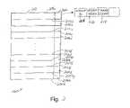
- FIG. 5 bis a diagrammatic representation of a group of “normal” blocks, a group of least frequently erased blocks, and a group of most frequently erased blocks in accordance with an embodiment of the present invention.
- a group of blocks 502includes blocks 514 which may be normal or static blocks which generally contain user data that may be erased but does not fall into the categories of a least frequently erased block or a most frequently erased block.
- a group least frequently erased blocks 506generally includes blocks 518 which have the lowest erase counts within an overall system, while a group of most frequently erased blocks 510 generally includes blocks 522 which have the highest erase counts of the erased blocks within the overall system. In general, blocks 518 are effectively used as spare blocks.
- erased block 514When a block 514 is erased, it may be determined whether erased block 514 has a relatively low associated erase count or a relatively high associated erase count. When erased block 514 has a relatively low associated erase count, erased block 514 may be added to group of least frequently erased blocks 506 . On the other hand, when erased block 514 has a relatively high associated erase count, erased block 514 may be reassigned to group of most frequently erased blocks 510 .
- Group of least frequently erased blocks 506which may be of substantially any size, may be a sorted group. That is, blocks 518 may be substantially sorted based on erase counts. The sorting is typically reflected in a corresponding least frequently erased block table (not shown) which contains entries associated with blocks 518 . For instance, each time a new block 518 is moved into or added to, or otherwise associated with, group of least frequently erased blocks 506 , blocks 518 may essentially be sorted based on erase counts such that the least frequently erased block 518 in group of least frequently erased blocks 506 may be the next block 518 to be reassigned, as for example to group 502 .
- the least erased block 518 of blocks 518is identified using a least frequently erased block table, and taken from group of least frequently erased blocks 506 .
- that block 514may be stored into group of least frequently erased blocks 506 , and the least frequently erased block table may be updated accordingly, i.e., an entry which corresponds to the added block may be included in the least frequently erased block table.
- Blocks 522 in group of most frequently erased blocks 510may also be substantially sorted based on erase counts.
- the sortingis typically implemented by sorting entries in a most frequently erased block table (not shown) which serves to identify blocks 522 .
- an average erase count associated with blocks 522may be calculated, i.e., an average erase count for group of most frequently erased blocks 510 may be determined.
- the erased block 514may be added to group of most frequently erased blocks 510 .
- a block 522 within group of frequently erased blocks 510 that has the lowest erase countmay be reassigned into group 502 . Such reassignments are typically reflected by updating an associated block mapping table, least frequently erased block table, and most frequently erased block table (not shown).
- the swapping of blocks between group 502 , group of least frequently erased blocks 506 , and most frequently erased blocks 510may generally occur when a block 514 included in group 502 is to be erased or updated. Alternatively, the swapping or updating of blocks may occur substantially any time it is desired for a spare block to be allocated for use in group 502 .
- FIG. 6one method of performing a block swap or update in an overall memory system such as a host system with embedded flash memory to allow for more even wear of the blocks will be described in accordance with an embodiment of the present invention.
- a process 600 of performing a block swap or updatebegins at step 604 in which a block, e.g., block “Y,” is “obtained” from a block mapping table or otherwise identified using the block mapping table.
- the block that is obtainedis the block that is to be effectively swapped out of the block mapping table for copying or updating its contents.
- a blocke.g., block “X”
- a spare blockis obtained from the group of least frequently erased blocks using the least frequently erased block table to identify an appropriate spare block.
- block “X”is the block with the lowest erase count in the group of least frequently erased blocks, although it should be appreciated that block “X” may be substantially any block associated with the group of least frequently erased blocks and, hence, the least frequently erased block table.
- the contents or, more specifically, data contents stored in block “Y” or new contents which are to replace the original contents of block “Y”are copied into block “X” in step 612 .
- block “X”is effectively moved into, or associated with, the block mapping table in step 616 .
- mappings associated with block “Y” and block “X”are effectively updated such that an LBA which was previously mapped to block “Y” is remapped to block “X.”
- block “Y”is erased in step 620 .
- the data contents, e.g., user contents, stored in block “Y”may be erased using substantially any suitable technique.
- the erase count associated with block “Y,” which is stored in a redundant area associated with block “Y,”is then incremented in step 624 to indicate that block “Y” has once again been erased. It should be appreciated that n one embodiment, an erase count for “Y” which is effectively stored in an erase count block may be updated.
- the block with the lowest erase count in the most frequently erased block tableis identified.
- blocks referenced in the most frequently erased block tableare sorted according to their respective erase counts. Sorting the blocks may include positioning the references to the blocks within the most frequently erased block table according to the erase counts of the blocks.
- identifying the block with the lowest erase countgenerally involves accessing the block reference in the position within the most frequently erased block table that is arranged to accommodate the block reference with the lowest erase count.
- step 628process flow moves from step 628 to step 632 in which it is determined if the erase count of block “Y” is greater than the erase count of the block with the lowest erase count referenced in the most frequently erased block table. If it is determined that the erase count of block “Y” is not greater than the erase count of the block with the lowest erase count referenced in the most frequently erased block table, then the indication is that block “Y” is not considered to be frequently erased.
- process flowproceeds from step 632 to step 636 in which block “Y” is moved into the group of least frequently erased blocks and effectively moved into the least frequently erased block table, i.e., an entry corresponding to block “Y” is added into the least frequently erased block table.
- moving block “Y” into the group of least frequently erased blocksmay include resorting substantially all block references in the least frequently erased block table using the erase count of each block. After block “Y” is effectively moved into the least frequently erased block table, the process of swapping or updating blocks is completed.
- step 632if the determination is step 632 is that the erase count of block “Y” exceeds the lowest erase count associated with the most frequently erased block table, the indication is that block “Y” should be moved into the group of most frequently erased blocks and effectively into the most frequently erased block table.
- a blocke.g., the block with the lowest erase count referenced in the most frequently erased block table, effectively needs to be removed from the most frequently erased block table.
- the block with the lowest erase count referenced in the most frequently erased block tableis moved into the group of least frequently erased blocks, and effectively moved into the least frequently erased block table. Moving the block into the group of least frequently erased blocks may include resorting the block references in the least frequently erased block table according to the erase count of each block.
- block “Y”is effectively moved into the most frequently erased block table in step 644 .
- moving block “Y” into the group of most frequently erased blocks and, hence, effectively into the most frequently erased block tablemay include resorting the most frequently erase blocks according to the erase count of each block, including block “Y.”
- block “Y”is effectively moved into the most frequently erased block table, the process of swapping or updating blocks is completed.
- a system architecture 700generally includes a variety of modules which may include, but are not limited to, an application interface module 704 , a system manager module 708 , a data manager module 712 , a data integrity manager 716 , and a device manager and interface module 720 .
- system architecture 700may be implemented using software code devices or firmware which may be accessed by a processor, e.g., processor 108 of FIG. 1 a.
- application interface module 704may be arranged to communicate with the host, operating system or the user directly.
- Application interface module 704is also in communication with system manager module 708 and data manager module 712 .
- system manager module 708When the user wants to read, write or format a flash memory, the user sends requests to the operating system, the requests are passed to the application interface module 704 .
- Application interface module 704directs the requests to system manager module 708 or data manager module 712 depending on the requests.
- System manager module 708includes a system initialization submodule 724 , an erase count block management submodule 726 , and a power management block submodule 730 .
- System initialization submodule 724is generally arranged to enable an initialization request to be processed, and typically communicates with erase count block management submodule 726 .
- system initialization submodule 724allows erase counts of blocks to be updated, and is substantially responsible for creating a least frequently erased block table and a most frequently erased block table.
- Erase count block management submodule 726includes functionality to cause erase counts of blocks to be stored, and functionality to cause an average erase count to be calculated, as well as updated, using individual erase counts. In other words, erase count block management submodule 726 effectively allows an average erase count to be maintained. Further, in one embodiment, erase count block management submodule 726 also substantially synchronizes the erase count of substantially all blocks in an erase count block during a power up of an overall system. While erase count block management submodule 726 may be arranged to cause an average erase count to be stored in an erase count block, it should be appreciated that power management block submodule 730 may instead be used to enable the average erase count to be stored.
- system manager module 708is also in communication with data manager module 712 , as well as device manager and interface module 720 .
- Data manager module 712which communicates with both system manager module 708 and application interface module 704 , may include functionality to provide page or block mapping.
- Data manager module 712may also include functionality associated with operating system and file system interface layers.
- Device manager and interface module 720which is in communication with system manager module 708 , data manager 712 , and data integrity manager 716 , typically provides a flash memory interface, and includes functionality associated with hardware abstractions, e.g., an I/O interface.
- Data integrity manager module 716provided ECC handling, among other functions.
- blocksmay instead be assigned to a most frequently erased block table and a least frequently erased block table based on a substantially absolute determination of which blocks have the highest erase counts and which blocks have the lowest erase counts, respectively.
- block erase countsmay effectively be compared against each other to determine an appropriate table in which to insert a block.
- a least frequently erased block tablehas generally been described as holding references to blocks with a relatively low erase count as spare blocks. Spare blocks are effectively allocated for use through the use of a block mapping table such that substantially any time a spare block is needed, the block with the lowest erase count referenced in the least frequently erased block table is provided for use.
- a refernece to the block with the lowest erase count in the group of least frequently erased blocksis moved into the block mapping table.
- substantially any blockmay generally be taken from the group of least frequently erased blocks during a block swapping or updating process. Selecting substantially any block from the least frequently erased blocks using the least frequently erased block table to move into the block mapping table may reduce the overhead associated with an overall system, as the blocks within the least frequently erased block table may not necessarily be sorted.
- Identifying and processing static blocksgenerally enhances the ability to enable blocks within an overall memory system to be worn evenly. In one embodiment, however, static blocks are not necessarily identified and processed. For example, if a relatively low number of static blocks is anticipated within a system, the identification and processing of static blocks may be substantially eliminated without departing from the spirit or the scope of the present invention.
- non-volatile memory systemshave been described as being controlled by associated memory controllers or being controlled using software or firmware associated with a host system, it should be understood that wear leveling processes which include erase count management may be applied to non-volatile memory systems which are in communication with controllers which are substantially external to the non-volatile memory systems.
- Suitable memory systems which use controllersinclude, but are not limited to, PC cards, CompactFlash cards, MultiMedia cards, Secure Digitalcards, and embedded chip sets which include flash memory and a flash memory controller.
- Memory systems which are controlled through the use of software or firmware loaded onto a host systeminclude embedded memory devices.
- memory systemswhich may use the erase management techniques described above and do not use controllers associated with the memory systems may use controllers associated with a host, e.g., a host computer system, to implement wear leveling. That is, a host may directly address and management memory in which wear leveling is to occur through the use of a controller on the host.
- a hoste.g., a host computer system
- processing static blocksmay not necessarily be included in the processing an initiation request.
- the determination of whether to effectively place a newly erased block into a most frequently erased block tablemay be based upon other criteria in lieu of being based upon whether the erased block has an erase count that is greater than the lowest erase count associated with the most frequently erased block table.
- such a determinationmay be based upon whether the erase count of the erased block exceeds an average erase count of substantially all blocks associated with the most frequently erased block table for a certain percentage, e.g., approximately twenty percent.
- a certain percentagee.g., approximately twenty percent.
- the block with the lowest erase count referenced in the most frequently erased block tablemay be moved into a least frequently erased block table, while the erased block is moved into the most frequently erased block table.
Landscapes
- Engineering & Computer Science (AREA)
- Theoretical Computer Science (AREA)
- Physics & Mathematics (AREA)
- General Engineering & Computer Science (AREA)
- General Physics & Mathematics (AREA)
- Techniques For Improving Reliability Of Storages (AREA)
- Read Only Memory (AREA)
- Radiation-Therapy Devices (AREA)
- Memory System Of A Hierarchy Structure (AREA)
- Filling Or Discharging Of Gas Storage Vessels (AREA)
- Non-Volatile Memory (AREA)
- Memory System (AREA)
Abstract
Description
Claims (31)
Priority Applications (11)
| Application Number | Priority Date | Filing Date | Title |
|---|---|---|---|
| US10/281,670US6973531B1 (en) | 2002-10-28 | 2002-10-28 | Tracking the most frequently erased blocks in non-volatile memory systems |
| AT03752244TATE387714T1 (en) | 2002-10-28 | 2003-09-10 | TRACKING THE MOST DERATED BLOCKS OF A NON-VOLATILE STORAGE SYSTEM |
| CNA038247844ACN1701390A (en) | 2002-10-28 | 2003-09-10 | Tracking the Most Frequently Erased Blocks in a Non-Volatile Memory System |
| PCT/US2003/028502WO2004040585A1 (en) | 2002-10-28 | 2003-09-10 | Tracking the most frequently erased blocks in non-volatile storage systems |
| AU2003270545AAU2003270545A1 (en) | 2002-10-28 | 2003-09-10 | Tracking the most frequently erased blocks in non-volatile storage systems |
| DE60319407TDE60319407T2 (en) | 2002-10-28 | 2003-09-10 | FOLLOW THE MOST CLEARED BLOCKS OF A NON-VOLATILE STORAGE SYSTEM |
| KR1020057007323AKR20050059314A (en) | 2002-10-28 | 2003-09-10 | Tracking the most frequently erased blocks in non-volatile storage systems |
| JP2004548320AJP2006504221A (en) | 2002-10-28 | 2003-09-10 | Tracking the most frequently erased blocks in non-volatile storage systems |
| EP03752244AEP1559113B1 (en) | 2002-10-28 | 2003-09-10 | Tracking the most frequently erased blocks in non-volatile storage systems |
| TW092125804ATWI267866B (en) | 2002-10-28 | 2003-09-18 | Tracking the most frequently erased blocks in non-volatile memory systems |
| JP2009202432AJP2010015591A (en) | 2002-10-28 | 2009-09-02 | Tracking of most frequently erased block in non-volatile storage system |
Applications Claiming Priority (1)
| Application Number | Priority Date | Filing Date | Title |
|---|---|---|---|
| US10/281,670US6973531B1 (en) | 2002-10-28 | 2002-10-28 | Tracking the most frequently erased blocks in non-volatile memory systems |
Publications (1)
| Publication Number | Publication Date |
|---|---|
| US6973531B1true US6973531B1 (en) | 2005-12-06 |
Family
ID=32228770
Family Applications (1)
| Application Number | Title | Priority Date | Filing Date |
|---|---|---|---|
| US10/281,670Expired - LifetimeUS6973531B1 (en) | 2002-10-28 | 2002-10-28 | Tracking the most frequently erased blocks in non-volatile memory systems |
Country Status (10)
| Country | Link |
|---|---|
| US (1) | US6973531B1 (en) |
| EP (1) | EP1559113B1 (en) |
| JP (2) | JP2006504221A (en) |
| KR (1) | KR20050059314A (en) |
| CN (1) | CN1701390A (en) |
| AT (1) | ATE387714T1 (en) |
| AU (1) | AU2003270545A1 (en) |
| DE (1) | DE60319407T2 (en) |
| TW (1) | TWI267866B (en) |
| WO (1) | WO2004040585A1 (en) |
Cited By (67)
| Publication number | Priority date | Publication date | Assignee | Title |
|---|---|---|---|---|
| US20040196723A1 (en)* | 2003-04-07 | 2004-10-07 | Eilert Sean S. | Dynamically mapping block-alterable memories |
| US7139863B1 (en)* | 2003-09-26 | 2006-11-21 | Storage Technology Corporation | Method and system for improving usable life of memory devices using vector processing |
| US20070083698A1 (en)* | 2002-10-28 | 2007-04-12 | Gonzalez Carlos J | Automated Wear Leveling in Non-Volatile Storage Systems |
| US20080126719A1 (en)* | 2006-11-24 | 2008-05-29 | Radoslav Danilak | System, method, and computer program product for delaying an operation that reduces a lifetime of memory |
| US20080126724A1 (en)* | 2006-11-24 | 2008-05-29 | Radoslav Danilak | System, method, and computer program product for reducing memory write operations using difference information |
| US20080126720A1 (en)* | 2006-11-24 | 2008-05-29 | Radoslav Danilak | Multi-memory device system and method for managing a lifetime thereof |
| US20080126685A1 (en)* | 2006-11-24 | 2008-05-29 | Radoslav Danilak | System, method, and computer program product for reducing memory write operations using an instruction set |
| US20080126891A1 (en)* | 2006-11-24 | 2008-05-29 | Radoslav Danilak | Memory lifetime gauging system, method and computer program product |
| US20080141055A1 (en)* | 2006-12-08 | 2008-06-12 | Radoslav Danilak | System and method for providing data redundancy after reducing memory writes |
| US20080141054A1 (en)* | 2006-12-08 | 2008-06-12 | Radoslav Danilak | System, method, and computer program product for providing data redundancy in a plurality of storage devices |
| US20080162796A1 (en)* | 2006-12-28 | 2008-07-03 | Genesys Logic, Inc. | Method for performing static wear leveling on flash memory |
| US20080235306A1 (en)* | 2007-03-20 | 2008-09-25 | Samsung Electronics Co., Ltd. | Garbage collection in nonvolatile memories using data attributes, computer program products and methods of operating the same |
| US20080231810A1 (en)* | 2007-03-19 | 2008-09-25 | Catania Louis J | Method of fitting contact lenses |
| US20080276035A1 (en)* | 2007-05-03 | 2008-11-06 | Atmel Corporation | Wear Leveling |
| US20080279005A1 (en)* | 2007-05-11 | 2008-11-13 | Spansion Llc | Managing flash memory program and erase cycles in the time domain |
| US20080282023A1 (en)* | 2007-05-09 | 2008-11-13 | Stmicroelectronics S.R.L. | Restoring storage devices based on flash memories and related circuit, system, and method |
| US20080282045A1 (en)* | 2007-05-09 | 2008-11-13 | Sudeep Biswas | Garbage collection in storage devices based on flash memories |
| US20080282024A1 (en)* | 2007-05-09 | 2008-11-13 | Sudeep Biswas | Management of erase operations in storage devices based on flash memories |
| US20080294813A1 (en)* | 2007-05-24 | 2008-11-27 | Sergey Anatolievich Gorobets | Managing Housekeeping Operations in Flash Memory |
| US20080294814A1 (en)* | 2007-05-24 | 2008-11-27 | Sergey Anatolievich Gorobets | Flash Memory System with Management of Housekeeping Operations |
| US20080313505A1 (en)* | 2007-06-14 | 2008-12-18 | Samsung Electronics Co., Ltd. | Flash memory wear-leveling |
| US20090129163A1 (en)* | 2007-11-19 | 2009-05-21 | Radoslav Danilak | System, method, and computer program product for increasing a lifetime of a plurality of blocks of memory |
| US20090132778A1 (en)* | 2007-11-19 | 2009-05-21 | Radoslav Danilak | System, method and a computer program product for writing data to different storage devices based on write frequency |
| CN101458969A (en)* | 2007-12-13 | 2009-06-17 | 三星电子株式会社 | Semiconductor memory system and wear-leveling method thereof |
| US20090164702A1 (en)* | 2007-12-21 | 2009-06-25 | Spansion Llc | Frequency distributed flash memory allocation based on free page tables |
| US20090327590A1 (en)* | 2008-06-25 | 2009-12-31 | Stec, Inc. | Enhanced mlc solid state device |
| US20100017588A1 (en)* | 2008-07-15 | 2010-01-21 | Radoslav Danilak | System, method, and computer program product for providing an extended capability to a system |
| US20100017566A1 (en)* | 2008-07-15 | 2010-01-21 | Radoslav Danilak | System, method, and computer program product for interfacing computing device hardware of a computing device and an operating system utilizing a virtualization layer |
| US20100023672A1 (en)* | 2007-11-13 | 2010-01-28 | Sergey Anatolievich Gorobets | Method And System For Virtual Fast Access Non-Volatile RAM |
| US20100064093A1 (en)* | 2008-09-09 | 2010-03-11 | Radoslav Danilak | System, method, and computer program product for converting data in a binary representation to a non-power of two representation |
| US20100146236A1 (en)* | 2008-12-08 | 2010-06-10 | Radoslav Danilak | System, method, and computer program product for rendering at least a portion of data useless in immediate response to a delete command |
| US20100161880A1 (en)* | 2006-12-27 | 2010-06-24 | Guangqing You | Flash initiative wear leveling algorithm |
| US20100185805A1 (en)* | 2007-07-05 | 2010-07-22 | Actions Semiconductor Co., Ltd. | Method And Apparatus For Performing Wear Leveling In Memory |
| US20100251009A1 (en)* | 2009-03-27 | 2010-09-30 | Ross John Stenfort | System, method, and computer program product for converting logical block address de-allocation information in a first format to a second format |
| US20100250830A1 (en)* | 2009-03-27 | 2010-09-30 | Ross John Stenfort | System, method, and computer program product for hardening data stored on a solid state disk |
| US20110004718A1 (en)* | 2009-07-02 | 2011-01-06 | Ross John Stenfort | System, method, and computer program product for ordering a plurality of write commands associated with a storage device |
| US20110004710A1 (en)* | 2009-07-06 | 2011-01-06 | Ross John Stenfort | System, method, and computer program product for interfacing one or more storage devices with a plurality of bridge chips |
| US20110016239A1 (en)* | 2009-07-20 | 2011-01-20 | Ross John Stenfort | System, method, and computer program product for reducing a rate of data transfer to at least a portion of memory |
| US20110016233A1 (en)* | 2009-07-17 | 2011-01-20 | Ross John Stenfort | System, method, and computer program product for inserting a gap in information sent from a drive to a host device |
| US20110029715A1 (en)* | 2009-07-29 | 2011-02-03 | International Business Machines Corporation | Write-erase endurance lifetime of memory storage devices |
| US20110055623A1 (en)* | 2009-09-03 | 2011-03-03 | Hynix Semiconductor Inc. | Solid state storage system with improved data merging efficiency and control method thereof |
| US20110078364A1 (en)* | 2009-09-30 | 2011-03-31 | Hynix Semiconductor Inc. | Solid state storage system for controlling reserved area flexibly and method for controlling the same |
| US20110082995A1 (en)* | 2009-10-06 | 2011-04-07 | Canon Kabushiki Kaisha | Information processing apparatus |
| US20110083047A1 (en)* | 2009-10-05 | 2011-04-07 | Ross John Stenfort | System, method, and computer program product for sending failure information from a serial ata (sata) solid state drive (ssd) to a host device |
| US20110087832A1 (en)* | 2007-05-09 | 2011-04-14 | Stmicroelectronics, S.R.L. | Wear leveling in storage devices based on flash memories and related circuit, system, and method |
| US20110138109A1 (en)* | 2009-12-07 | 2011-06-09 | Chao-Yin Liu | Method for wear-leveling and apparatus thereof |
| US8230159B2 (en) | 2009-03-27 | 2012-07-24 | Lsi Corporation | System, method, and computer program product for sending logical block address de-allocation status information |
| CN102929794A (en)* | 2012-09-26 | 2013-02-13 | 惠州市德赛西威汽车电子有限公司 | Storage method for electrically erasable programmable read only memory (EEPROM) |
| US20130311702A1 (en)* | 2012-05-18 | 2013-11-21 | Silicon Motion, Inc. | Data storage device and method for flash block management |
| TWI416528B (en)* | 2009-01-07 | 2013-11-21 | Silicon Motion Inc | Method for operating non-volatile memory and data storage system using the same |
| US8671259B2 (en) | 2009-03-27 | 2014-03-11 | Lsi Corporation | Storage system data hardening |
| US8677054B1 (en)* | 2009-12-16 | 2014-03-18 | Apple Inc. | Memory management schemes for non-volatile memory devices |
| TWI475569B (en)* | 2006-11-24 | 2015-03-01 | Lsi Corp | System, method, and computer program product for delaying an operation that reduces a lifetime of memory |
| US20150113207A1 (en)* | 2013-10-17 | 2015-04-23 | SK Hynix Inc. | Operating method of data storage device |
| US20150277785A1 (en)* | 2014-03-31 | 2015-10-01 | Phison Electronics Corp. | Data writing method, memory control circuit unit and memory storage apparatus |
| US9183133B2 (en) | 2007-11-28 | 2015-11-10 | Seagate Technology Llc | System, method, and computer program product for increasing spare space in memory to extend a lifetime of the memory |
| US20160139826A1 (en)* | 2014-11-13 | 2016-05-19 | Micron Technology, Inc. | Memory Wear Leveling |
| US9454492B2 (en) | 2006-12-06 | 2016-09-27 | Longitude Enterprise Flash S.A.R.L. | Systems and methods for storage parallelism |
| US9495241B2 (en) | 2006-12-06 | 2016-11-15 | Longitude Enterprise Flash S.A.R.L. | Systems and methods for adaptive data storage |
| US9766819B2 (en) | 2014-12-30 | 2017-09-19 | Sandisk Technologies Llc | Systems and methods for managing storage endurance |
| US9875039B2 (en) | 2014-09-30 | 2018-01-23 | Sandisk Technologies Llc | Method and apparatus for wear-leveling non-volatile memory |
| US10019353B2 (en) | 2012-03-02 | 2018-07-10 | Longitude Enterprise Flash S.A.R.L. | Systems and methods for referencing data on a storage medium |
| US10133663B2 (en) | 2010-12-17 | 2018-11-20 | Longitude Enterprise Flash S.A.R.L. | Systems and methods for persistent address space management |
| US10338817B2 (en) | 2014-12-30 | 2019-07-02 | Sandisk Technologies Llc | Systems and methods for storage recovery |
| US10558371B2 (en) | 2006-12-06 | 2020-02-11 | Fio Semiconductor Technologies, Llc | Apparatus, system, and method for data block usage information synchronization for a non-volatile storage volume |
| US11061663B2 (en)* | 2017-12-12 | 2021-07-13 | Cypress Semiconductor Corporation | Memory devices, systems, and methods for updating firmware with single memory device |
| US11231856B2 (en)* | 2016-03-09 | 2022-01-25 | Kioxia Corporation | Storage system having a host that manages physical data locations of a storage device |
Families Citing this family (23)
| Publication number | Priority date | Publication date | Assignee | Title |
|---|---|---|---|---|
| US7441067B2 (en) | 2004-11-15 | 2008-10-21 | Sandisk Corporation | Cyclic flash memory wear leveling |
| US7315917B2 (en) | 2005-01-20 | 2008-01-01 | Sandisk Corporation | Scheduling of housekeeping operations in flash memory systems |
| US7224604B2 (en)* | 2005-03-14 | 2007-05-29 | Sandisk Il Ltd. | Method of achieving wear leveling in flash memory using relative grades |
| US7516267B2 (en)* | 2005-11-03 | 2009-04-07 | Intel Corporation | Recovering from a non-volatile memory failure |
| US7640389B2 (en)* | 2006-02-28 | 2009-12-29 | Freescale Semiconductor, Inc. | Non-volatile memory having a multiple block erase mode and method therefor |
| CN101211314B (en)* | 2006-12-31 | 2010-07-14 | 创惟科技股份有限公司 | Method for prolonging flash memory data read-write life |
| CN100504814C (en) | 2007-01-17 | 2009-06-24 | 忆正存储技术(深圳)有限公司 | Flash block management method |
| JP4762261B2 (en) | 2008-03-12 | 2011-08-31 | 株式会社東芝 | Memory system |
| JP2009266349A (en) | 2008-04-28 | 2009-11-12 | Toshiba Corp | Nonvolatile semiconductor memory device |
| KR20100013485A (en) | 2008-07-31 | 2010-02-10 | 삼성전자주식회사 | Memory device and method of wear leveling |
| US8700840B2 (en) | 2009-01-05 | 2014-04-15 | SanDisk Technologies, Inc. | Nonvolatile memory with write cache having flush/eviction methods |
| US8244960B2 (en) | 2009-01-05 | 2012-08-14 | Sandisk Technologies Inc. | Non-volatile memory and method with write cache partition management methods |
| US8094500B2 (en) | 2009-01-05 | 2012-01-10 | Sandisk Technologies Inc. | Non-volatile memory and method with write cache partitioning |
| TWI409819B (en) | 2009-03-03 | 2013-09-21 | Silicon Motion Inc | Method of evenly using a plurality of blocks of a flash memory, and associated memory device and controller thereof |
| CN101989458B (en)* | 2009-07-31 | 2013-10-30 | 慧帝科技(深圳)有限公司 | Method and memory device for averagely using plurality of blocks of flash memory, and controller |
| US9170933B2 (en)* | 2010-06-28 | 2015-10-27 | International Business Machines Corporation | Wear-level of cells/pages/sub-pages/blocks of a memory |
| KR20120096212A (en)* | 2011-02-22 | 2012-08-30 | 삼성전자주식회사 | Non-volatile memory device, memory controller, and methods thereof |
| GB2490991B (en)* | 2011-05-19 | 2017-08-30 | Ibm | Wear leveling |
| KR101989018B1 (en)* | 2012-06-25 | 2019-06-13 | 에스케이하이닉스 주식회사 | Operating method for data storage device |
| US8750045B2 (en) | 2012-07-27 | 2014-06-10 | Sandisk Technologies Inc. | Experience count dependent program algorithm for flash memory |
| ES2898395T3 (en)* | 2016-12-09 | 2022-03-07 | Roche Diabetes Care Gmbh | Device to perform at least one medical action |
| CN111261218B (en)* | 2020-04-27 | 2020-08-21 | 深圳市芯天下技术有限公司 | Method for simultaneously testing multiple Norflash samples |
| DE102021116828A1 (en) | 2021-06-30 | 2023-01-05 | Harman Becker Automotive Systems Gmbh | Method and device for monitoring a payload of a storage medium |
Citations (24)
| Publication number | Priority date | Publication date | Assignee | Title |
|---|---|---|---|---|
| JPS62283497A (en) | 1986-05-31 | 1987-12-09 | Canon Inc | Memory write control method |
| JPS62283496A (en) | 1986-05-31 | 1987-12-09 | Canon Inc | Programmable read-only memory write count management method |
| US5222109A (en) | 1990-12-28 | 1993-06-22 | Ibm Corporation | Endurance management for solid state files |
| US5297148A (en) | 1989-04-13 | 1994-03-22 | Sundisk Corporation | Flash eeprom system |
| US5388083A (en) | 1993-03-26 | 1995-02-07 | Cirrus Logic, Inc. | Flash memory mass storage architecture |
| US5438573A (en) | 1991-09-13 | 1995-08-01 | Sundisk Corporation | Flash EEPROM array data and header file structure |
| US5485595A (en) | 1993-03-26 | 1996-01-16 | Cirrus Logic, Inc. | Flash memory mass storage architecture incorporating wear leveling technique without using cam cells |
| US5568423A (en)* | 1995-04-14 | 1996-10-22 | Unisys Corporation | Flash memory wear leveling system providing immediate direct access to microprocessor |
| US5568439A (en) | 1988-06-08 | 1996-10-22 | Harari; Eliyahou | Flash EEPROM system which maintains individual memory block cycle counts |
| US5598370A (en) | 1993-02-24 | 1997-01-28 | International Business Machines Corporation | Nonvolatile memory with cluster-erase flash capability and solid state file apparatus using the same |
| US5737742A (en)* | 1994-06-29 | 1998-04-07 | Hitachi, Ltd. | Memory system using flash memory and method of controlling the memory system |
| US5832493A (en) | 1997-04-24 | 1998-11-03 | Trimble Navigation Limited | Flash file management system |
| US5835935A (en) | 1995-09-13 | 1998-11-10 | Lexar Media, Inc. | Method of and architecture for controlling system data with automatic wear leveling in a semiconductor non-volatile mass storage memory |
| US5845313A (en) | 1995-07-31 | 1998-12-01 | Lexar | Direct logical block addressing flash memory mass storage architecture |
| US5860082A (en) | 1996-03-28 | 1999-01-12 | Datalight, Inc. | Method and apparatus for allocating storage in a flash memory |
| US5907856A (en) | 1995-07-31 | 1999-05-25 | Lexar Media, Inc. | Moving sectors within a block of information in a flash memory mass storage architecture |
| US5956473A (en)* | 1996-11-25 | 1999-09-21 | Macronix International Co., Ltd. | Method and system for managing a flash memory mass storage system |
| US5963473A (en)* | 1996-05-23 | 1999-10-05 | Micron Technology, Inc. | Flash memory system and method for monitoring the disturb effect on memory cell blocks due to high voltage conditions of other memory cell blocks |
| US6016275A (en) | 1998-03-13 | 2000-01-18 | Lg Semicon Co., Ltd. | Flash memory wear leveling system and method |
| US6081447A (en) | 1991-09-13 | 2000-06-27 | Western Digital Corporation | Wear leveling techniques for flash EEPROM systems |
| US6125435A (en) | 1995-09-13 | 2000-09-26 | Lexar Media, Inc. | Alignment of cluster address to block addresses within a semiconductor non-volatile mass storage memory |
| US6260156B1 (en) | 1998-12-04 | 2001-07-10 | Datalight, Inc. | Method and system for managing bad areas in flash memory |
| US6426893B1 (en) | 2000-02-17 | 2002-07-30 | Sandisk Corporation | Flash eeprom system with simultaneous multiple data sector programming and storage of physical block characteristics in other designated blocks |
| US6732221B2 (en)* | 2001-06-01 | 2004-05-04 | M-Systems Flash Disk Pioneers Ltd | Wear leveling of static areas in flash memory |
Family Cites Families (1)
| Publication number | Priority date | Publication date | Assignee | Title |
|---|---|---|---|---|
| JP2002032256A (en)* | 2000-07-19 | 2002-01-31 | Matsushita Electric Ind Co Ltd | Terminal device |
- 2002
- 2002-10-28USUS10/281,670patent/US6973531B1/ennot_activeExpired - Lifetime
- 2003
- 2003-09-10CNCNA038247844Apatent/CN1701390A/enactivePending
- 2003-09-10DEDE60319407Tpatent/DE60319407T2/ennot_activeExpired - Fee Related
- 2003-09-10AUAU2003270545Apatent/AU2003270545A1/ennot_activeAbandoned
- 2003-09-10WOPCT/US2003/028502patent/WO2004040585A1/enactiveIP Right Grant
- 2003-09-10KRKR1020057007323Apatent/KR20050059314A/ennot_activeWithdrawn
- 2003-09-10EPEP03752244Apatent/EP1559113B1/ennot_activeExpired - Lifetime
- 2003-09-10ATAT03752244Tpatent/ATE387714T1/ennot_activeIP Right Cessation
- 2003-09-10JPJP2004548320Apatent/JP2006504221A/enactivePending
- 2003-09-18TWTW092125804Apatent/TWI267866B/ennot_activeIP Right Cessation
- 2009
- 2009-09-02JPJP2009202432Apatent/JP2010015591A/enactivePending
Patent Citations (28)
| Publication number | Priority date | Publication date | Assignee | Title |
|---|---|---|---|---|
| JPS62283496A (en) | 1986-05-31 | 1987-12-09 | Canon Inc | Programmable read-only memory write count management method |
| JPS62283497A (en) | 1986-05-31 | 1987-12-09 | Canon Inc | Memory write control method |
| US5568439A (en) | 1988-06-08 | 1996-10-22 | Harari; Eliyahou | Flash EEPROM system which maintains individual memory block cycle counts |
| US5297148A (en) | 1989-04-13 | 1994-03-22 | Sundisk Corporation | Flash eeprom system |
| US5222109A (en) | 1990-12-28 | 1993-06-22 | Ibm Corporation | Endurance management for solid state files |
| US6081447A (en) | 1991-09-13 | 2000-06-27 | Western Digital Corporation | Wear leveling techniques for flash EEPROM systems |
| US5438573A (en) | 1991-09-13 | 1995-08-01 | Sundisk Corporation | Flash EEPROM array data and header file structure |
| US6230233B1 (en) | 1991-09-13 | 2001-05-08 | Sandisk Corporation | Wear leveling techniques for flash EEPROM systems |
| US5598370A (en) | 1993-02-24 | 1997-01-28 | International Business Machines Corporation | Nonvolatile memory with cluster-erase flash capability and solid state file apparatus using the same |
| US5485595A (en) | 1993-03-26 | 1996-01-16 | Cirrus Logic, Inc. | Flash memory mass storage architecture incorporating wear leveling technique without using cam cells |
| US5388083A (en) | 1993-03-26 | 1995-02-07 | Cirrus Logic, Inc. | Flash memory mass storage architecture |
| US5930193A (en)* | 1994-06-29 | 1999-07-27 | Hitachi, Ltd. | Memory system using a flash memory and method of controlling the memory system |
| US5737742A (en)* | 1994-06-29 | 1998-04-07 | Hitachi, Ltd. | Memory system using flash memory and method of controlling the memory system |
| US5568423A (en)* | 1995-04-14 | 1996-10-22 | Unisys Corporation | Flash memory wear leveling system providing immediate direct access to microprocessor |
| US6115785A (en) | 1995-07-31 | 2000-09-05 | Lexar Media, Inc. | Direct logical block addressing flash memory mass storage architecture |
| US5907856A (en) | 1995-07-31 | 1999-05-25 | Lexar Media, Inc. | Moving sectors within a block of information in a flash memory mass storage architecture |
| US5924113A (en) | 1995-07-31 | 1999-07-13 | Lexar Media, Inc. | Direct logical block addressing flash memory mass storage architecture |
| US5845313A (en) | 1995-07-31 | 1998-12-01 | Lexar | Direct logical block addressing flash memory mass storage architecture |
| US6125435A (en) | 1995-09-13 | 2000-09-26 | Lexar Media, Inc. | Alignment of cluster address to block addresses within a semiconductor non-volatile mass storage memory |
| US5835935A (en) | 1995-09-13 | 1998-11-10 | Lexar Media, Inc. | Method of and architecture for controlling system data with automatic wear leveling in a semiconductor non-volatile mass storage memory |
| US5860082A (en) | 1996-03-28 | 1999-01-12 | Datalight, Inc. | Method and apparatus for allocating storage in a flash memory |
| US5963473A (en)* | 1996-05-23 | 1999-10-05 | Micron Technology, Inc. | Flash memory system and method for monitoring the disturb effect on memory cell blocks due to high voltage conditions of other memory cell blocks |
| US5956473A (en)* | 1996-11-25 | 1999-09-21 | Macronix International Co., Ltd. | Method and system for managing a flash memory mass storage system |
| US5832493A (en) | 1997-04-24 | 1998-11-03 | Trimble Navigation Limited | Flash file management system |
| US6016275A (en) | 1998-03-13 | 2000-01-18 | Lg Semicon Co., Ltd. | Flash memory wear leveling system and method |
| US6260156B1 (en) | 1998-12-04 | 2001-07-10 | Datalight, Inc. | Method and system for managing bad areas in flash memory |
| US6426893B1 (en) | 2000-02-17 | 2002-07-30 | Sandisk Corporation | Flash eeprom system with simultaneous multiple data sector programming and storage of physical block characteristics in other designated blocks |
| US6732221B2 (en)* | 2001-06-01 | 2004-05-04 | M-Systems Flash Disk Pioneers Ltd | Wear leveling of static areas in flash memory |
Non-Patent Citations (1)
| Title |
|---|
| Kim, Jesung et al., "A Space-Efficient Flash Translation Layer for Compactflash Systems", IEEE Transactions on Consumer Electronics, vol. 48, No. 2, May 2002. |
Cited By (141)
| Publication number | Priority date | Publication date | Assignee | Title |
|---|---|---|---|---|
| US7552272B2 (en) | 2002-10-28 | 2009-06-23 | Sandisk Corporation | Automated wear leveling in non-volatile storage systems |
| US20070083698A1 (en)* | 2002-10-28 | 2007-04-12 | Gonzalez Carlos J | Automated Wear Leveling in Non-Volatile Storage Systems |
| US7328301B2 (en)* | 2003-04-07 | 2008-02-05 | Intel Corporation | Dynamically mapping block-alterable memories |
| US20040196723A1 (en)* | 2003-04-07 | 2004-10-07 | Eilert Sean S. | Dynamically mapping block-alterable memories |
| US7139863B1 (en)* | 2003-09-26 | 2006-11-21 | Storage Technology Corporation | Method and system for improving usable life of memory devices using vector processing |
| US8230183B2 (en) | 2006-11-24 | 2012-07-24 | Lsi Corporation | Techniques for prolonging a lifetime of memory by controlling operations that affect the lifetime of the memory |
| US20080126719A1 (en)* | 2006-11-24 | 2008-05-29 | Radoslav Danilak | System, method, and computer program product for delaying an operation that reduces a lifetime of memory |
| US20080126685A1 (en)* | 2006-11-24 | 2008-05-29 | Radoslav Danilak | System, method, and computer program product for reducing memory write operations using an instruction set |
| US20080126891A1 (en)* | 2006-11-24 | 2008-05-29 | Radoslav Danilak | Memory lifetime gauging system, method and computer program product |
| US8402184B2 (en) | 2006-11-24 | 2013-03-19 | Lsi Corporation | Techniques for reducing memory write operations using coalescing memory buffers and difference information |
| US20080126724A1 (en)* | 2006-11-24 | 2008-05-29 | Radoslav Danilak | System, method, and computer program product for reducing memory write operations using difference information |
| US8230164B2 (en) | 2006-11-24 | 2012-07-24 | Lsi Corporation | Techniques for multi-memory device lifetime management |
| US20080126720A1 (en)* | 2006-11-24 | 2008-05-29 | Radoslav Danilak | Multi-memory device system and method for managing a lifetime thereof |
| US20110167199A1 (en)* | 2006-11-24 | 2011-07-07 | Sandforce Inc. | Techniques for prolonging a lifetime of memory by controlling operations that affect the lifetime of the memory |
| US20110125956A1 (en)* | 2006-11-24 | 2011-05-26 | Sandforce Inc. | Techniques for multi-memory device lifetime management |
| US7904619B2 (en) | 2006-11-24 | 2011-03-08 | Sandforce, Inc. | System, method, and computer program product for reducing memory write operations using difference information |
| US7904764B2 (en) | 2006-11-24 | 2011-03-08 | Sandforce, Inc. | Memory lifetime gauging system, method and computer program product |
| TWI475569B (en)* | 2006-11-24 | 2015-03-01 | Lsi Corp | System, method, and computer program product for delaying an operation that reduces a lifetime of memory |
| US7809900B2 (en) | 2006-11-24 | 2010-10-05 | Sandforce, Inc. | System, method, and computer program product for delaying an operation that reduces a lifetime of memory |
| US7747813B2 (en) | 2006-11-24 | 2010-06-29 | Sandforce, Inc. | Multi-memory device system and method for managing a lifetime thereof |
| US11847066B2 (en) | 2006-12-06 | 2023-12-19 | Unification Technologies Llc | Apparatus, system, and method for managing commands of solid-state storage using bank interleave |
| US10387327B2 (en) | 2006-12-06 | 2019-08-20 | Fio Semiconductor Technologies, Llc | Systems and methods for identifying storage resources that are not in use |
| US11640359B2 (en) | 2006-12-06 | 2023-05-02 | Unification Technologies Llc | Systems and methods for identifying storage resources that are not in use |
| US9454492B2 (en) | 2006-12-06 | 2016-09-27 | Longitude Enterprise Flash S.A.R.L. | Systems and methods for storage parallelism |
| US9495241B2 (en) | 2006-12-06 | 2016-11-15 | Longitude Enterprise Flash S.A.R.L. | Systems and methods for adaptive data storage |
| US11960412B2 (en) | 2006-12-06 | 2024-04-16 | Unification Technologies Llc | Systems and methods for identifying storage resources that are not in use |
| US9575902B2 (en) | 2006-12-06 | 2017-02-21 | Longitude Enterprise Flash S.A.R.L. | Apparatus, system, and method for managing commands of solid-state storage using bank interleave |
| US11573909B2 (en) | 2006-12-06 | 2023-02-07 | Unification Technologies Llc | Apparatus, system, and method for managing commands of solid-state storage using bank interleave |
| US9632727B2 (en) | 2006-12-06 | 2017-04-25 | Longitude Enterprise Flash S.A.R.L. | Systems and methods for identifying storage resources that are not in use |
| US10558371B2 (en) | 2006-12-06 | 2020-02-11 | Fio Semiconductor Technologies, Llc | Apparatus, system, and method for data block usage information synchronization for a non-volatile storage volume |
| US8504783B2 (en) | 2006-12-08 | 2013-08-06 | Lsi Corporation | Techniques for providing data redundancy after reducing memory writes |
| US8090980B2 (en) | 2006-12-08 | 2012-01-03 | Sandforce, Inc. | System, method, and computer program product for providing data redundancy in a plurality of storage devices |
| US20080141054A1 (en)* | 2006-12-08 | 2008-06-12 | Radoslav Danilak | System, method, and computer program product for providing data redundancy in a plurality of storage devices |
| US20080141055A1 (en)* | 2006-12-08 | 2008-06-12 | Radoslav Danilak | System and method for providing data redundancy after reducing memory writes |
| US7904672B2 (en) | 2006-12-08 | 2011-03-08 | Sandforce, Inc. | System and method for providing data redundancy after reducing memory writes |
| US8356152B2 (en) | 2006-12-27 | 2013-01-15 | Intel Corporation | Initiative wear leveling for non-volatile memory |
| US20100161880A1 (en)* | 2006-12-27 | 2010-06-24 | Guangqing You | Flash initiative wear leveling algorithm |
| US20080162796A1 (en)* | 2006-12-28 | 2008-07-03 | Genesys Logic, Inc. | Method for performing static wear leveling on flash memory |
| US8700839B2 (en)* | 2006-12-28 | 2014-04-15 | Genesys Logic, Inc. | Method for performing static wear leveling on flash memory |
| US20080231810A1 (en)* | 2007-03-19 | 2008-09-25 | Catania Louis J | Method of fitting contact lenses |
| US20080235306A1 (en)* | 2007-03-20 | 2008-09-25 | Samsung Electronics Co., Ltd. | Garbage collection in nonvolatile memories using data attributes, computer program products and methods of operating the same |
| US7689762B2 (en) | 2007-05-03 | 2010-03-30 | Atmel Corporation | Storage device wear leveling |
| US20080276035A1 (en)* | 2007-05-03 | 2008-11-06 | Atmel Corporation | Wear Leveling |
| US20110289266A1 (en)* | 2007-05-09 | 2011-11-24 | Stmicroelectronics Pvt. Ltd. | Garbage collection in storage devices based on flash memories |
| US20080282045A1 (en)* | 2007-05-09 | 2008-11-13 | Sudeep Biswas | Garbage collection in storage devices based on flash memories |
| US8041883B2 (en) | 2007-05-09 | 2011-10-18 | Stmicroelectronics S.R.L. | Restoring storage devices based on flash memories and related circuit, system, and method |
| US9146854B2 (en) | 2007-05-09 | 2015-09-29 | Stmicroelectronics International N.V. | Restoring storage devices based on flash memories and related circuit, system, and method |
| US7991942B2 (en)* | 2007-05-09 | 2011-08-02 | Stmicroelectronics S.R.L. | Memory block compaction method, circuit, and system in storage devices based on flash memories |
| US20110087832A1 (en)* | 2007-05-09 | 2011-04-14 | Stmicroelectronics, S.R.L. | Wear leveling in storage devices based on flash memories and related circuit, system, and method |
| US8954649B2 (en)* | 2007-05-09 | 2015-02-10 | SK Hynix Inc. | Garbage collection in storage devices based on flash memories |
| US20080282024A1 (en)* | 2007-05-09 | 2008-11-13 | Sudeep Biswas | Management of erase operations in storage devices based on flash memories |
| US20080282023A1 (en)* | 2007-05-09 | 2008-11-13 | Stmicroelectronics S.R.L. | Restoring storage devices based on flash memories and related circuit, system, and method |
| US8099545B2 (en) | 2007-05-09 | 2012-01-17 | Stmicroelectronics S.R.L. | Wear leveling in storage devices based on flash memories and related circuit, system, and method |
| US20080279005A1 (en)* | 2007-05-11 | 2008-11-13 | Spansion Llc | Managing flash memory program and erase cycles in the time domain |
| US7743203B2 (en) | 2007-05-11 | 2010-06-22 | Spansion Llc | Managing flash memory based upon usage history |
| US20080294813A1 (en)* | 2007-05-24 | 2008-11-27 | Sergey Anatolievich Gorobets | Managing Housekeeping Operations in Flash Memory |
| US20080294814A1 (en)* | 2007-05-24 | 2008-11-27 | Sergey Anatolievich Gorobets | Flash Memory System with Management of Housekeeping Operations |
| US20080313505A1 (en)* | 2007-06-14 | 2008-12-18 | Samsung Electronics Co., Ltd. | Flash memory wear-leveling |
| TWI474324B (en)* | 2007-06-14 | 2015-02-21 | Samsung Electronics Co Ltd | A method of wear-leveling memory device and memory system |
| US7797481B2 (en)* | 2007-06-14 | 2010-09-14 | Samsung Electronics Co., Ltd. | Method and apparatus for flash memory wear-leveling using logical groups |
| US8296539B2 (en)* | 2007-07-05 | 2012-10-23 | Actions Semiconductor Co., Ltd. | Method and apparatus for performing wear leveling in memory |
| US20100185805A1 (en)* | 2007-07-05 | 2010-07-22 | Actions Semiconductor Co., Ltd. | Method And Apparatus For Performing Wear Leveling In Memory |
| US8296498B2 (en) | 2007-11-13 | 2012-10-23 | Sandisk Technologies Inc. | Method and system for virtual fast access non-volatile RAM |
| US20100023672A1 (en)* | 2007-11-13 | 2010-01-28 | Sergey Anatolievich Gorobets | Method And System For Virtual Fast Access Non-Volatile RAM |
| US8339881B2 (en) | 2007-11-19 | 2012-12-25 | Lsi Corporation | Techniques for increasing a lifetime of blocks of memory |
| US7903486B2 (en) | 2007-11-19 | 2011-03-08 | Sandforce, Inc. | System, method, and computer program product for increasing a lifetime of a plurality of blocks of memory |
| US20090132778A1 (en)* | 2007-11-19 | 2009-05-21 | Radoslav Danilak | System, method and a computer program product for writing data to different storage devices based on write frequency |
| US20090129163A1 (en)* | 2007-11-19 | 2009-05-21 | Radoslav Danilak | System, method, and computer program product for increasing a lifetime of a plurality of blocks of memory |
| US7849275B2 (en) | 2007-11-19 | 2010-12-07 | Sandforce, Inc. | System, method and a computer program product for writing data to different storage devices based on write frequency |
| US8230184B2 (en) | 2007-11-19 | 2012-07-24 | Lsi Corporation | Techniques for writing data to different portions of storage devices based on write frequency |
| US10318181B2 (en) | 2007-11-28 | 2019-06-11 | Seagate Technology Llc | System, method, and computer program product for increasing spare space in memory to extend a lifetime of the memory |
| US9183133B2 (en) | 2007-11-28 | 2015-11-10 | Seagate Technology Llc | System, method, and computer program product for increasing spare space in memory to extend a lifetime of the memory |
| US9645750B2 (en) | 2007-11-28 | 2017-05-09 | Seagate Technology Llc | System, method, and computer program product for increasing spare space in memory to extend a lifetime of the memory |
| US8055836B2 (en) | 2007-12-13 | 2011-11-08 | Samsung Electronics Co., Ltd. | Semiconductor memory system and wear-leveling method thereof |
| CN101458969A (en)* | 2007-12-13 | 2009-06-17 | 三星电子株式会社 | Semiconductor memory system and wear-leveling method thereof |
| US20090157952A1 (en)* | 2007-12-13 | 2009-06-18 | Samsung Electronics Co., Ltd. | Semiconductor memory system and wear-leveling method thereof |
| CN101458969B (en)* | 2007-12-13 | 2013-06-19 | 三星电子株式会社 | Semiconductor memory system and wear-leveling method thereof |
| US8656083B2 (en)* | 2007-12-21 | 2014-02-18 | Spansion Llc | Frequency distributed flash memory allocation based on free page tables |
| US20090164702A1 (en)* | 2007-12-21 | 2009-06-25 | Spansion Llc | Frequency distributed flash memory allocation based on free page tables |
| US20090327591A1 (en)* | 2008-06-25 | 2009-12-31 | Stec, Inc. | Slc-mlc combination flash storage device |
| US20090327590A1 (en)* | 2008-06-25 | 2009-12-31 | Stec, Inc. | Enhanced mlc solid state device |
| US8825941B2 (en) | 2008-06-25 | 2014-09-02 | Stec, Inc. | SLC-MLC combination flash storage device |
| US8762622B2 (en)* | 2008-06-25 | 2014-06-24 | Stec, Inc. | Enhanced MLC solid state device |
| US20100017588A1 (en)* | 2008-07-15 | 2010-01-21 | Radoslav Danilak | System, method, and computer program product for providing an extended capability to a system |
| US20100017566A1 (en)* | 2008-07-15 | 2010-01-21 | Radoslav Danilak | System, method, and computer program product for interfacing computing device hardware of a computing device and an operating system utilizing a virtualization layer |
| US20100064093A1 (en)* | 2008-09-09 | 2010-03-11 | Radoslav Danilak | System, method, and computer program product for converting data in a binary representation to a non-power of two representation |
| US20100146236A1 (en)* | 2008-12-08 | 2010-06-10 | Radoslav Danilak | System, method, and computer program product for rendering at least a portion of data useless in immediate response to a delete command |
| TWI416528B (en)* | 2009-01-07 | 2013-11-21 | Silicon Motion Inc | Method for operating non-volatile memory and data storage system using the same |
| US8230159B2 (en) | 2009-03-27 | 2012-07-24 | Lsi Corporation | System, method, and computer program product for sending logical block address de-allocation status information |
| US8671259B2 (en) | 2009-03-27 | 2014-03-11 | Lsi Corporation | Storage system data hardening |
| US8090905B2 (en) | 2009-03-27 | 2012-01-03 | Sandforce, Inc. | System, method, and computer program product for converting logical block address de-allocation information in a first format to a second format |
| US20100250830A1 (en)* | 2009-03-27 | 2010-09-30 | Ross John Stenfort | System, method, and computer program product for hardening data stored on a solid state disk |
| US20100251009A1 (en)* | 2009-03-27 | 2010-09-30 | Ross John Stenfort | System, method, and computer program product for converting logical block address de-allocation information in a first format to a second format |
| US20110004718A1 (en)* | 2009-07-02 | 2011-01-06 | Ross John Stenfort | System, method, and computer program product for ordering a plurality of write commands associated with a storage device |
| US8930606B2 (en) | 2009-07-02 | 2015-01-06 | Lsi Corporation | Ordering a plurality of write commands associated with a storage device |
| US9792074B2 (en) | 2009-07-06 | 2017-10-17 | Seagate Technology Llc | System, method, and computer program product for interfacing one or more storage devices with a plurality of bridge chips |
| US20110004710A1 (en)* | 2009-07-06 | 2011-01-06 | Ross John Stenfort | System, method, and computer program product for interfacing one or more storage devices with a plurality of bridge chips |
| US8140712B2 (en) | 2009-07-17 | 2012-03-20 | Sandforce, Inc. | System, method, and computer program product for inserting a gap in information sent from a drive to a host device |
| US20110016233A1 (en)* | 2009-07-17 | 2011-01-20 | Ross John Stenfort | System, method, and computer program product for inserting a gap in information sent from a drive to a host device |
| US20110016239A1 (en)* | 2009-07-20 | 2011-01-20 | Ross John Stenfort | System, method, and computer program product for reducing a rate of data transfer to at least a portion of memory |
| US8516166B2 (en) | 2009-07-20 | 2013-08-20 | Lsi Corporation | System, method, and computer program product for reducing a rate of data transfer to at least a portion of memory |
| CN102473135A (en)* | 2009-07-29 | 2012-05-23 | 国际商业机器公司 | Write-erase endurance life of storage devices |
| US8402242B2 (en)* | 2009-07-29 | 2013-03-19 | International Business Machines Corporation | Write-erase endurance lifetime of memory storage devices |
| TWI489468B (en)* | 2009-07-29 | 2015-06-21 | Sk Hynix Inc | Write-erase endurance lifetime of memory storage devices |
| US20110029715A1 (en)* | 2009-07-29 | 2011-02-03 | International Business Machines Corporation | Write-erase endurance lifetime of memory storage devices |
| US9776673B2 (en) | 2009-07-29 | 2017-10-03 | SK Hynix Inc. | Write-erase endurance lifetime of memory storage devices |
| US20110055623A1 (en)* | 2009-09-03 | 2011-03-03 | Hynix Semiconductor Inc. | Solid state storage system with improved data merging efficiency and control method thereof |
| US8214698B2 (en) | 2009-09-03 | 2012-07-03 | Hynix Semiconductor Inc. | Solid state storage system with improved data merging efficiency and control method thereof |
| US20110078364A1 (en)* | 2009-09-30 | 2011-03-31 | Hynix Semiconductor Inc. | Solid state storage system for controlling reserved area flexibly and method for controlling the same |
| US8392647B2 (en) | 2009-09-30 | 2013-03-05 | Hynix Semiconductor Inc. | Solid state storage system for controlling reserved area flexibly and method for controlling the same |
| US20110083047A1 (en)* | 2009-10-05 | 2011-04-07 | Ross John Stenfort | System, method, and computer program product for sending failure information from a serial ata (sata) solid state drive (ssd) to a host device |
| US8108737B2 (en) | 2009-10-05 | 2012-01-31 | Sandforce, Inc. | System, method, and computer program product for sending failure information from a serial ATA (SATA) solid state drive (SSD) to a host device |
| US20110082995A1 (en)* | 2009-10-06 | 2011-04-07 | Canon Kabushiki Kaisha | Information processing apparatus |
| US20110138109A1 (en)* | 2009-12-07 | 2011-06-09 | Chao-Yin Liu | Method for wear-leveling and apparatus thereof |
| US8677054B1 (en)* | 2009-12-16 | 2014-03-18 | Apple Inc. | Memory management schemes for non-volatile memory devices |
| US10133663B2 (en) | 2010-12-17 | 2018-11-20 | Longitude Enterprise Flash S.A.R.L. | Systems and methods for persistent address space management |
| US10019353B2 (en) | 2012-03-02 | 2018-07-10 | Longitude Enterprise Flash S.A.R.L. | Systems and methods for referencing data on a storage medium |
| US20130311702A1 (en)* | 2012-05-18 | 2013-11-21 | Silicon Motion, Inc. | Data storage device and method for flash block management |
| US9104549B2 (en)* | 2012-05-18 | 2015-08-11 | Silicon Motion, Inc. | Data storage device and method for flash block management |
| US20130311703A1 (en)* | 2012-05-18 | 2013-11-21 | Silicon Motion, Inc. | Data storage device and method for flash block management |
| US9223691B2 (en)* | 2012-05-18 | 2015-12-29 | Silicon Motion, Inc. | Data storage device and method for flash block management |
| US20130311698A1 (en)* | 2012-05-18 | 2013-11-21 | Silicon Motion, Inc. | Data storage device and method for flash block management |
| US9116792B2 (en)* | 2012-05-18 | 2015-08-25 | Silicon Motion, Inc. | Data storage device and method for flash block management |
| CN102929794B (en)* | 2012-09-26 | 2015-12-02 | 惠州市德赛西威汽车电子股份有限公司 | The storage means of a kind of EEPROM |
| CN102929794A (en)* | 2012-09-26 | 2013-02-13 | 惠州市德赛西威汽车电子有限公司 | Storage method for electrically erasable programmable read only memory (EEPROM) |
| US20150113207A1 (en)* | 2013-10-17 | 2015-04-23 | SK Hynix Inc. | Operating method of data storage device |
| US20150277785A1 (en)* | 2014-03-31 | 2015-10-01 | Phison Electronics Corp. | Data writing method, memory control circuit unit and memory storage apparatus |
| US9298610B2 (en)* | 2014-03-31 | 2016-03-29 | Phison Electronics Corp. | Data writing method, memory control circuit unit and memory storage apparatus |
| US9875039B2 (en) | 2014-09-30 | 2018-01-23 | Sandisk Technologies Llc | Method and apparatus for wear-leveling non-volatile memory |
| US10635326B2 (en) | 2014-09-30 | 2020-04-28 | Sandisk Technologies Llc | Method and apparatus for wear-levelling non-volatile memory |
| US20160139826A1 (en)* | 2014-11-13 | 2016-05-19 | Micron Technology, Inc. | Memory Wear Leveling |
| US20180067661A1 (en)* | 2014-11-13 | 2018-03-08 | Micron Technology, Inc. | Memory wear leveling |
| US9830087B2 (en)* | 2014-11-13 | 2017-11-28 | Micron Technology, Inc. | Memory wear leveling |
| US10268396B2 (en) | 2014-12-30 | 2019-04-23 | Sandisk Technologies Llc | Systems and methods for managing storage endurance |
| US10338817B2 (en) | 2014-12-30 | 2019-07-02 | Sandisk Technologies Llc | Systems and methods for storage recovery |
| US9766819B2 (en) | 2014-12-30 | 2017-09-19 | Sandisk Technologies Llc | Systems and methods for managing storage endurance |
| US11231856B2 (en)* | 2016-03-09 | 2022-01-25 | Kioxia Corporation | Storage system having a host that manages physical data locations of a storage device |
| US11768610B2 (en) | 2016-03-09 | 2023-09-26 | Kioxia Corporation | Storage system having a host that manages physical data locations of a storage device |
| US12073093B2 (en) | 2016-03-09 | 2024-08-27 | Kioxia Corporation | Storage system having a host that manages physical data locations of a storage device |
| US12399629B2 (en) | 2016-03-09 | 2025-08-26 | Kioxia Corporation | Storage system having a host that manages physical data locations of a storage device |
| US11061663B2 (en)* | 2017-12-12 | 2021-07-13 | Cypress Semiconductor Corporation | Memory devices, systems, and methods for updating firmware with single memory device |
Also Published As
| Publication number | Publication date |
|---|---|
| KR20050059314A (en) | 2005-06-17 |
| WO2004040585A1 (en) | 2004-05-13 |
| JP2010015591A (en) | 2010-01-21 |
| DE60319407T2 (en) | 2009-03-19 |
| EP1559113B1 (en) | 2008-02-27 |
| DE60319407D1 (en) | 2008-04-10 |
| TW200418038A (en) | 2004-09-16 |
| CN1701390A (en) | 2005-11-23 |
| JP2006504221A (en) | 2006-02-02 |
| AU2003270545A1 (en) | 2004-05-25 |
| ATE387714T1 (en) | 2008-03-15 |
| TWI267866B (en) | 2006-12-01 |
| EP1559113A1 (en) | 2005-08-03 |
Similar Documents
| Publication | Publication Date | Title |
|---|---|---|
| US6973531B1 (en) | Tracking the most frequently erased blocks in non-volatile memory systems | |
| US7096313B1 (en) | Tracking the least frequently erased blocks in non-volatile memory systems | |
| US6985992B1 (en) | Wear-leveling in non-volatile storage systems | |
| US7287118B2 (en) | Maintaining an average erase count in a non-volatile storage system | |
| US7103732B1 (en) | Method and apparatus for managing an erase count block | |
| US6831865B2 (en) | Maintaining erase counts in non-volatile storage systems | |
| US7039788B1 (en) | Method and apparatus for splitting a logical block |
Legal Events
| Date | Code | Title | Description |
|---|---|---|---|
| AS | Assignment | Owner name:SANDISK CORPORATION, CALIFORNIA Free format text:ASSIGNMENT OF ASSIGNORS INTEREST;ASSIGNORS:CHANG, ROBERT C.;QAWAMI, BAHMAN;SABET-SHARGHI, FARSHID;REEL/FRAME:013434/0102;SIGNING DATES FROM 20020610 TO 20020611 | |
| STCF | Information on status: patent grant | Free format text:PATENTED CASE | |
| FPAY | Fee payment | Year of fee payment:4 | |
| AS | Assignment | Owner name:SANDISK TECHNOLOGIES INC., TEXAS Free format text:ASSIGNMENT OF ASSIGNORS INTEREST;ASSIGNOR:SANDISK CORPORATION;REEL/FRAME:026334/0062 Effective date:20110404 | |
| FPAY | Fee payment | Year of fee payment:8 | |
| AS | Assignment | Owner name:INTELLIGENT INTELLECTUAL PROPERTY HOLDINGS LLC., D Free format text:ASSIGNMENT OF ASSIGNORS INTEREST;ASSIGNOR:SANDISK TECHNOLOGIES, INC.;REEL/FRAME:030953/0416 Effective date:20130801 | |
| AS | Assignment | Owner name:INTELLIGENT INTELLECTUAL PROPERTY HOLDINGS LLC., D Free format text:CORRECTIVE ASSIGNMENT TO CORRECT THE ADDRESS OF THE ASSIGNOR IN THE ASSIGNMENT DOCUMENT PREVIOUSLY RECORDED ON REEL 030953 FRAME 0416. ASSIGNOR(S) HEREBY CONFIRMS THE ASSIGNMENT;ASSIGNOR:SANDISK TECHNOLOGIES, INC.;REEL/FRAME:030994/0046 Effective date:20130801 | |
| AS | Assignment | Owner name:SANDISK CORPORATION, CALIFORNIA Free format text:SECURITY AGREEMENT;ASSIGNOR:INTELLIGENT INTELLECTUAL PROPERTY HOLDINGS LLC;REEL/FRAME:031074/0651 Effective date:20130820 | |
| AS | Assignment | Owner name:PS3 LUXCO SARL, LUXEMBOURG Free format text:ASSIGNMENT OF ASSIGNORS INTEREST;ASSIGNOR:INTELLIGENT INTELLECTUAL PROPERTY HOLDINGS LLC;REEL/FRAME:031723/0836 Effective date:20130821 | |
| AS | Assignment | Owner name:PS2 LUXCO SARL, LUXEMBOURG Free format text:ASSIGNMENT OF ASSIGNORS INTEREST;ASSIGNOR:PS3 LUXCO SARL;REEL/FRAME:031734/0555 Effective date:20130821 | |
| AS | Assignment | Owner name:LONGITUDE FLASH MEMORY SYSTEMS S.A.R.L., LUXEMBOUR Free format text:CHANGE OF NAME;ASSIGNOR:PS2 LUXCO S.A.R.L.;REEL/FRAME:031814/0068 Effective date:20131112 | |
| AS | Assignment | Owner name:SANDISK TECHNOLOGIES, INC., TEXAS Free format text:ASSIGNMENT OF ASSIGNORS INTEREST;ASSIGNOR:LONGITUDE FLASH MEMORY SYSTEMS SARL;REEL/FRAME:038166/0445 Effective date:20160318 | |
| AS | Assignment | Owner name:SANDISK TECHNOLOGIES LLC, TEXAS Free format text:CHANGE OF NAME;ASSIGNOR:SANDISK TECHNOLOGIES INC;REEL/FRAME:038813/0004 Effective date:20160516 | |
| AS | Assignment | Owner name:SANDISK CORPORATION, CALIFORNIA Free format text:TERMINATION AND RELEASE OF SECURITY INTEREST IN PATENTS;ASSIGNORS:SANDISK CORPORATION;SANDISK TECHNOLOGIES, INC.;REEL/FRAME:038825/0137 Effective date:20160427 | |
| FPAY | Fee payment | Year of fee payment:12 | |
| SULP | Surcharge for late payment | Year of fee payment:11 |