US6970366B2 - Phase-shifted resonant converter having reduced output ripple - Google Patents
Phase-shifted resonant converter having reduced output rippleDownload PDFInfo
- Publication number
- US6970366B2 US6970366B2US10/407,047US40704703AUS6970366B2US 6970366 B2US6970366 B2US 6970366B2US 40704703 AUS40704703 AUS 40704703AUS 6970366 B2US6970366 B2US 6970366B2
- Authority
- US
- United States
- Prior art keywords
- resonant
- power
- power switch
- converter
- circuit
- Prior art date
- Legal status (The legal status is an assumption and is not a legal conclusion. Google has not performed a legal analysis and makes no representation as to the accuracy of the status listed.)
- Expired - Lifetime, expires
Links
- 239000003990capacitorSubstances0.000claimsabstractdescription94
- 238000004804windingMethods0.000claimsdescription28
- 230000008859changeEffects0.000description3
- 230000009977dual effectEffects0.000description3
- 230000010363phase shiftEffects0.000description3
- 208000032365Electromagnetic interferenceDiseases0.000description2
- 238000005259measurementMethods0.000description2
- 230000009467reductionEffects0.000description2
- 230000001105regulatory effectEffects0.000description2
- 230000004913activationEffects0.000description1
- 230000006978adaptationEffects0.000description1
- 230000003466anti-cipated effectEffects0.000description1
- 230000008878couplingEffects0.000description1
- 238000010168coupling processMethods0.000description1
- 238000005859coupling reactionMethods0.000description1
- 230000000694effectsEffects0.000description1
- 230000004048modificationEffects0.000description1
- 238000012986modificationMethods0.000description1
- 230000004044responseEffects0.000description1
Images


Classifications
- H—ELECTRICITY
- H02—GENERATION; CONVERSION OR DISTRIBUTION OF ELECTRIC POWER
- H02M—APPARATUS FOR CONVERSION BETWEEN AC AND AC, BETWEEN AC AND DC, OR BETWEEN DC AND DC, AND FOR USE WITH MAINS OR SIMILAR POWER SUPPLY SYSTEMS; CONVERSION OF DC OR AC INPUT POWER INTO SURGE OUTPUT POWER; CONTROL OR REGULATION THEREOF
- H02M3/00—Conversion of DC power input into DC power output
- H02M3/22—Conversion of DC power input into DC power output with intermediate conversion into AC
- H02M3/24—Conversion of DC power input into DC power output with intermediate conversion into AC by static converters
- H02M3/28—Conversion of DC power input into DC power output with intermediate conversion into AC by static converters using discharge tubes with control electrode or semiconductor devices with control electrode to produce the intermediate AC
- H02M3/285—Single converters with a plurality of output stages connected in parallel
- Y—GENERAL TAGGING OF NEW TECHNOLOGICAL DEVELOPMENTS; GENERAL TAGGING OF CROSS-SECTIONAL TECHNOLOGIES SPANNING OVER SEVERAL SECTIONS OF THE IPC; TECHNICAL SUBJECTS COVERED BY FORMER USPC CROSS-REFERENCE ART COLLECTIONS [XRACs] AND DIGESTS
- Y02—TECHNOLOGIES OR APPLICATIONS FOR MITIGATION OR ADAPTATION AGAINST CLIMATE CHANGE
- Y02B—CLIMATE CHANGE MITIGATION TECHNOLOGIES RELATED TO BUILDINGS, e.g. HOUSING, HOUSE APPLIANCES OR RELATED END-USER APPLICATIONS
- Y02B70/00—Technologies for an efficient end-user side electric power management and consumption
- Y02B70/10—Technologies improving the efficiency by using switched-mode power supplies [SMPS], i.e. efficient power electronics conversion e.g. power factor correction or reduction of losses in power supplies or efficient standby modes
- Y—GENERAL TAGGING OF NEW TECHNOLOGICAL DEVELOPMENTS; GENERAL TAGGING OF CROSS-SECTIONAL TECHNOLOGIES SPANNING OVER SEVERAL SECTIONS OF THE IPC; TECHNICAL SUBJECTS COVERED BY FORMER USPC CROSS-REFERENCE ART COLLECTIONS [XRACs] AND DIGESTS
- Y02—TECHNOLOGIES OR APPLICATIONS FOR MITIGATION OR ADAPTATION AGAINST CLIMATE CHANGE
- Y02P—CLIMATE CHANGE MITIGATION TECHNOLOGIES IN THE PRODUCTION OR PROCESSING OF GOODS
- Y02P80/00—Climate change mitigation technologies for sector-wide applications
- Y02P80/10—Efficient use of energy, e.g. using compressed air or pressurized fluid as energy carrier
Definitions
- the present inventionrelates to switched mode power converter circuits, and more particularly, to a phase-shifted half bridge resonant converter that provides a DC output voltage having minimal ripple.
- Switched mode power convertersare known in the art to convert an available direct current (DC) level voltage to another DC level voltage.
- a switched mode power converterprovides a regulated DC output voltage to a load by selectively storing energy in an inductor coupled to the load by switching the flow of current into the inductor.
- a resonant converteris one particular type of switched mode power converter that includes a resonant circuit including a capacitor and an inductor. Current is periodically delivered to the resonant circuit by operation of one or more power switches typically provided by MOSFET transistors.
- the loadmay be isolated from the resonant circuit using a transformer having a primary winding that provides all or part of the inductance portion of the resonant circuit.
- a sinusoidal current waveform present on the secondary winding of the transformeris rectified and delivered to the load as a DC output.
- the output voltage and/or currentmay be regulated in response to changing load conditions by altering the switching frequency applied to the power switch to thereby control the amount of current delivered to the resonant circuit.
- Resonant convertersare particularly advantageous for high power applications since they produce relatively low electro-magnetic interference (EMI), have almost zero switching losses of the power switches, and have a generally robust design.
- EMIelectro-magnetic interference
- a drawback of resonant converter circuitsis that the output current generally has ripple that is unacceptable for certain applications.
- the rectified sinusoidal waveformis smoothed by a filter capacitor coupled in parallel with the load.
- the ripple current into the filter capacitoris relatively large in comparison with the DC output current.
- the filter capacitormust remove a relatively large portion of the current delivered from the resonant circuit, resulting in inefficiency of the resonant converter circuit and increasing the size and capacity of the filter capacitor.
- resonant converter circuitshave limited output voltage regulation window.
- the resonant circuithas a characteristic Q curve (i.e., impedance vs. frequency).
- the average switching frequencyis set either above or below resonance on the side of the Q curve.
- Output voltage regulationis accomplished by moving the switching frequency along the side of the Q curve to change the amplitude of the current in the resonant circuit.
- the load range of the outputcorresponds to the frequency range of the resonant circuit. If the resonant circuit has a narrow frequency range, then the load range is also narrow, which makes resonant converters less useful in applications where load varies over a wide range.
- resonant converter circuitsrelates to the voltage regulation window under no-load condition. Under this condition, the resonant converter can go into hard switching with increased voltage and current stress on the power switches as well as increases of conducted and radiated noise. In the worst case, the load has to be increased to 20-40% of max load for a proper function of the resonant converter. Also, the voltage stress on the power switches is proportional to the load range. When there is a short of the output voltage, the voltage across the resonant capacitor can quickly rise above the input voltage, causing failure of the power switches.
- a power converterthat has substantially reduced ripple current in comparison to conventional resonant converter circuits.
- the power convertercomprises a pair of resonant converter circuits coupled together in parallel and operated at respective switching frequencies that are out of phase.
- the power converterincludes a first resonant converter circuit and a second resonant converter circuit operatively coupled together.
- the first resonant converter circuitincludes at least one power switch adapted to convey power to a first resonant circuit and a first rectification stage adapted to rectify the conveyed power from the first resonant circuit.
- the second resonant converter circuitincludes at least one power switch adapted to convey power to a second resonant circuit and a second rectification stage adapted to rectify the conveyed power from the second resonant circuit.
- a filter capacitoris coupled to the first and second rectification stages to provide DC output power therefrom.
- a regulatoris operatively coupled to the first and second resonant converters to control switching frequency of the power switches, such that the switching frequency of the at least one power switch of the second resonant converter is shifted in phase with respect to the switching frequency of the at least one power switch of the second resonant converter.
- the switching frequency of the at least one power switch of the second resonant converteris shifted in phase by approximately 90° with respect to the switching frequency of the at least one power switch of the second resonant converter.
- the first and second resonant circuitseach further comprises an inductor, a transformer having a primary winding in series with the inductor, and first and second capacitors in series with the primary winding and connected across an input voltage source.
- an overvoltage condition of at least one of the first and second resonant converter circuitsis prevented by including first and second diodes coupled in parallel respectively with the first and second capacitors. The diodes serves to couple to ground excess current in the resonant circuit when an overvoltage condition is experienced.
- an additional capacitoris operatively coupled between the primary winding and the first and second capacitors, in order to prevent frequency shift of the resonant circuit upon shorting of one of the first and second capacitors upon the overvoltage condition.
- additional first and second capacitorsare coupled in series respectively with the first and second capacitors.
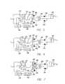
- FIG. 1depicts a prior art resonant converter circuit
- FIG. 2is a graph depicting the ripple current in a filter capacitor of the prior art resonant converter circuit
- FIG. 3depicts a multiple-phase resonant converter circuit in accordance with an embodiment of the invention
- FIG. 4is a graph depicting the ripple current in a filter capacitor of the multiple-phase resonant converter circuit
- FIG. 5depicts a resonant converter circuit providing resonant circuit overvoltage protection in accordance with an alternative embodiment of the invention
- FIG. 6depicts a resonant converter circuit providing resonant circuit overvoltage protection in accordance with another alternative embodiment of the invention.
- FIG. 7depicts a resonant converter circuit providing resonant circuit overvoltage protection in accordance with yet another alternative embodiment of the invention.
- the present inventionprovides a resonant converter circuit having reduced ripple current for use in high output power applications and that has improved voltage regulation.
- like element numeralsare used to describe like elements illustrated in one or more of the figures.
- FIG. 1depicts a resonant converter circuit 10 in accordance with the prior art.
- the resonant converter 10converts an input DC voltage V in to an output DC voltage V out applied to a load (not shown).
- the resonant converter 10includes a pair of power switches 12 , 14 , typically provided by MOSFET devices.
- the drain terminal of the high side power switch 12is coupled to the input voltage V in
- the source terminal of the low side power switch 14is connected to ground
- the respective source and drain terminals of the power switches 12 , 14are coupled together to define a phase node.
- the phase nodeis coupled to a resonant circuit that includes inductor 16 , the primary winding of transformer 26 , and capacitors 32 , 34 .
- Inductor 16is coupled in series with the primary winding.
- Capacitor 32is connected between the primary winding and the input voltage V in , and capacitor 32 is connected between the primary winding and ground.
- the secondary winding of transformer 26includes a center tap defining an isolated ground, and positive and negative taps coupled to respective rectifying diodes 36 , 38 .
- the rectifying diodes 36 , 38are coupled together to define an output terminal that provides the output voltage V out , with filter capacitor 42 coupled between the output terminal and the isolated ground.
- a driver 22alternatingly drives the gate terminals of the power switches 12 , 14 .
- a regulator 24controls the driver 22 .
- the opening and closing of the power switches 12 , 14provides an intermediate voltage having a rectangular waveform at the phase node.
- the regulator 24may include a feedback loop that derives measurements of the output voltage V out or output current I out and uses that information to control the switching frequency applied to the power switches 12 , 14 in order to regulate the output voltage V out and/or output current I out at desired levels.
- the rectangular waveform at the phase nodeproduces a resonance in the resonant circuit, resulting in a sinusoidal current waveform being present on the secondary winding of the transformer 26 .
- the sinusoidal current waveformis rectified by diodes 36 , 38 and smoothed by capacitor 42 to provide the DC output voltage V out .
- the power switches 12 , 14are alternatingly driven in accordance with a half-bridge power cycle in which a dead time period occurs between successive positive and negative going periods.
- the power switches 12 , 14respectively have both an internal body capacitance (not shown) and an external snubber capacitor 13 , 15 . These two capacitances are referred to collectively as the snubber capacitor of the power switch.
- power switch 12is turned on at a time in which the voltage across its snubber capacitor is at zero. This causes the snubber capacitor of power switch 14 to charge to the input voltage V in .
- power switch 14is turned off, causing the snubber capacitor of power switch 12 to discharge and the snubber capacitor of power switch 14 to charge. After the voltage across the snubber capacitor of power switch 12 falls to zero, current is conducted through the body diode of power switch 12 and power switch 12 is turned on. The power cycle continuously repeats in this same manner.
- the exemplary resonant converter circuit 10generally has a switching frequency above the resonant frequency.
- the switching frequencyranges from 125 kHz to 325 kHz.
- the length of the dead time between successive activation periods of the power switches 12 , 14is optimized as a function of the switching frequency to achieve zero voltage switching.
- I pis the sinusoidal current waveform on the secondary winding of the transformer 26 and I out is the DC output current.
- the ripple current I r into the filter capacitor 42is roughly 48.5% of the DC output current I out .
- FIG. 2illustrates the rectified sinusoidal waveform on the secondary winding of the transformer 26 .
- the shaded regionscorrespond to the ripple current I r .
- the filter capacitor 42must remove a relatively large portion of the current delivered from the resonant circuit, resulting in inefficiency of the resonant converter circuit 10 and a large power-loss in the filter capacitor 42 . This necessarily requires the size and capacity of the filter capacitor 42 to be increased.
- the multiple-phase resonant converter circuit 100essentially comprises two separate resonant converter circuits coupled in parallel and operating out of phase by 90° so that the rectified sinusoidal waveforms will overlap and thereby reduce the ripple current into the filter capacitors.
- Each of the two separate resonant converter circuitsis constructed substantially as described above with respect to FIG. 1 .
- a first resonant converterincludes a pair of power switches 112 , 114 in which the drain terminal of the high side power switch 112 is coupled to the input voltage V in , the source terminal of the low side power switch 114 is connected to ground, and the respective source and drain terminals of the power switches 112 , 114 are coupled together to define a first phase node.
- Snubber capacitors 113 , 115are shown coupled across power switches 112 , 114 , respectively, as described above with respect to FIG. 1 .
- the first phase nodeis coupled to a first resonant circuit that includes inductor 132 , the primary winding of transformer 146 , and capacitors 136 , 138 .
- the secondary winding of transformer 146includes a center tap defining an isolated ground, and positive and negative taps coupled to respective rectifying diodes 152 , 154 .
- a second resonant converterincludes a pair of power switches 116 , 118 in which the drain terminal of the high side power switch 116 is coupled to the input voltage V in , the source terminal of the low side power switch 118 is connected to ground, and the respective source and drain terminals of the power switches 116 , 118 are coupled together to define a second phase node.
- Snubber capacitors 117 , 119are shown coupled across power switches 116 , 118 , respectively, as described above with respect to FIG. 1 .
- the second phase nodeis coupled to a second resonant circuit that includes inductor 134 , the primary winding of transformer 148 , and capacitors 142 , 144 .
- the secondary winding of transformer 148includes a center tap defining an isolated ground, and positive and negative taps coupled to respective rectifying diodes 156 , 158 .
- the rectifying diodes 152 , 154 , 156 , 158are coupled together to define an output terminal that provides the output voltage V out , with filter capacitor 162 coupled between the output terminal and the isolated ground.
- a first driver 122alternatingly drives the gate terminals of the power switches 112 , 114
- a second driver 124alternatingly drives the gate terminals of the power switches 116 , 118
- a regulator 126controls the first and second drivers 122 , 124 such that they have a predetermined phase difference.
- the predetermined phase differenceis 90°, but it should be appreciated that other phase differences could also be advantageously utilized.
- the rectangular waveform at the first and second phase nodesproduces resonance in the respective resonant circuits, resulting in sinusoidal current waveforms being present on the secondary windings of transformers 146 , 148 .
- the sinusoidal current waveformsare rectified by diodes 152 , 154 , 156 , 158 and smoothed by capacitor 162 to provide the DC output voltage V out .
- the regulator 126may include a feedback loop that derives measurements of the output voltage V out or output current I out and uses that information to control the switching frequency applied to the power switches 112 , 114 , 116 , 118 in order to regulate the output voltage V out and/or output current I out at desired levels.
- Matching the resonant circuit componentsi.e., inductors 132 , 134 , capacitors 136 , 138 , 142 , 144 , and transformers 146 , 148 , may accomplish effective current sharing between the two resonant converters.
- phase shift devicesuch as the Unitrode UCC3895 device, may provide the regulator 126 .
- any commercially available phase shift devicecapable of changing the frequency, dead time control and duty cycle of driver outputs while maintaining a constant 90° phase shift between driver outputs to the resonant stages could be advantageously utilized. It may also be advantageous for certain applications to utilize two separate regulators operating out of phase by 90°, instead of a single regulator, although this solution may not be desirable from a cost perspective.
- the ripple current I r into the filter capacitor 162is approximately 9.5% of the DC output current I out , i.e., a substantial reduction in ripple current from the prior art resonant converter circuit.
- FIG. 4illustrates the two phase-shifted rectified sinusoidal waveforms on the secondary windings of the transformers 146 , 148 .
- the shaded regionscorrespond to the ripple current I r , which clearly shows that the filter capacitor 162 need only remove a relatively small portion of the current delivered from the resonant circuits.
- phase-shifted resonant converter of the present inventionwould achieve low levels of ripple current roughly equivalent to that of conventional forward, half-bridge, and full bridge converters, while at the same time utilizing resonant inductors (i.e., chokes) substantially smaller than these conventional devices.
- resonant inductorsi.e., chokes
- the phase-shifted resonant converter of the present inventioncan be utilized in relatively compact units.
- the voltage across the resonant capacitors 32 , 34can rise above the input voltage V in , causing failure of one or both of the power switches 12 , 14 due to presence of voltage across the device during turn on. Specifically, the voltage across one of the resonant capacitors (e.g., capacitor 32 ) rises above the input voltage V in , while the voltage across the other one of the resonant capacitors (e.g., capacitor 34 ) reverses. This causes excess current to conduct through the associated power switch (e.g., switch 14 ), resulting in failure of the switch.
- the associated power switche.g., switch 14
- FIGS. 5-7depict alternative embodiments of the invention in which the resonant converter circuit is additionally provided with overvoltage protection.
- Each of these figuresdepicts a single resonant converter circuit rather than the dual phase-shifted resonant converter configuration described above with regard to FIG. 3 . It should be understood that single resonant converter circuits are shown for the sake of simplicity, and that it is intended that the overvoltage protection circuitry of FIGS. 5-7 be implemented as part of the dual resonant converter circuit described above.
- FIG. 5illustrates a resonant converter circuit providing resonant circuit overvoltage protection in accordance with an alternative embodiment of the invention.
- the resonant converter circuit of FIG. 5corresponds to a portion of the dual phase-shifted resonant converter of FIG. 3 .
- the embodiment of FIG. 5further includes diodes 162 , 164 connected in parallel with resonant capacitors 136 , 138 , respectively.
- the diodes 162 , 164provide overvoltage protection for the power switches 112 , 114 .
- the voltage across one of the resonant capacitors 136 , 138rises above the input voltage V in , while the voltage across the other one of the resonant capacitors 136 , 138 reverses.
- the reversed voltage across one of the resonant capacitors 136 , 138will be discharged through the associated diode 162 , 164 , causing the voltage across the other resonant capacitor to equalize at the input voltage V in .
- Thishas the effect of clamping the voltage across the resonant capacitor to the input voltage V in .
- the inductor 132acts as a current limiter (i.e., choke) to limit the current that passes through the resonant circuit, thereby limiting the current drawn through the power switches 112 , 114 in the event of an overvoltage condition.
- a current limiteri.e., choke
- FIG. 6illustrates a resonant converter circuit providing resonant circuit overvoltage protection in accordance with another alternative embodiment of the invention.
- the embodiment of FIG. 6is substantially the same as that of FIG. 5 , except that an additional capacitor 166 is included within the resonant circuit in series with the primary winding of transformer 146 .
- the associated capacitoris effectively shorted. This causes the resonant frequency of the resonant circuit to shift due to the reduction in the capacitive portion of the resonant circuit.
- the additional capacitor 166serves to retain the capacitive portion in the event of a short of one of the resonant capacitors 136 , 138 .
- the capacitance of the additional capacitor 166 and each of capacitors 136 , 138is selected such that shorting of one of capacitors 136 , 138 would have limited or no substantial change on the total capacitance of the resonant circuit.
- FIG. 7illustrates a resonant converter circuit providing resonant circuit overvoltage protection in accordance with yet another alternative embodiment of the invention.
- the embodiment of FIG. 7is substantially the same as that of FIG. 6 , except that the additional capacitor is included as two separate additional capacitors 172 , 174 connected in series with the capacitors 136 , 138 , respectively.
- the additional capacitors 172 , 174provide the same function as the additional capacitor 166 of FIG. 6 , i.e., to retain the capacitive portion in the event of a short of one of the resonant capacitors 136 , 138 .
- the capacitances of the additional capacitors 172 , 174 and each of capacitors 136 , 138are selected such that shorting of one of capacitors 136 , 138 would have limited or no substantial change on the total capacitance of the resonant circuit.
Landscapes
- Engineering & Computer Science (AREA)
- Power Engineering (AREA)
- Dc-Dc Converters (AREA)
- Structure Of Transmissions (AREA)
Abstract
Description
wherein Ipis the sinusoidal current waveform on the secondary winding of the
wherein Ipis the sinusoidal current waveform on the secondary winding of the
Claims (10)
Priority Applications (6)
| Application Number | Priority Date | Filing Date | Title |
|---|---|---|---|
| US10/407,047US6970366B2 (en) | 2003-04-03 | 2003-04-03 | Phase-shifted resonant converter having reduced output ripple |
| EP04725215AEP1609235B1 (en) | 2003-04-03 | 2004-04-01 | Phase-shifted resonant converter having reduced output ripple |
| DE602004030228TDE602004030228D1 (en) | 2003-04-03 | 2004-04-01 | PHASE-SHIFTED RESONANCE CONVERTER WITH REDUCED OUTPUT SHAFT |
| PCT/NO2004/000097WO2004088828A2 (en) | 2003-04-03 | 2004-04-01 | Phase-shifted resonant converter having reduced output ripple |
| AT04725215TATE489765T1 (en) | 2003-04-03 | 2004-04-01 | PHASE-SHIFT RESONANCE CONVERTER WITH REDUCED OUTPUT RIPPLE |
| NO20055126ANO331890B1 (en) | 2003-04-03 | 2005-11-02 | Phase-turned resonant converter with reduced output ripple |
Applications Claiming Priority (1)
| Application Number | Priority Date | Filing Date | Title |
|---|---|---|---|
| US10/407,047US6970366B2 (en) | 2003-04-03 | 2003-04-03 | Phase-shifted resonant converter having reduced output ripple |
Publications (2)
| Publication Number | Publication Date |
|---|---|
| US20040196679A1 US20040196679A1 (en) | 2004-10-07 |
| US6970366B2true US6970366B2 (en) | 2005-11-29 |
Family
ID=33097460
Family Applications (1)
| Application Number | Title | Priority Date | Filing Date |
|---|---|---|---|
| US10/407,047Expired - LifetimeUS6970366B2 (en) | 2003-04-03 | 2003-04-03 | Phase-shifted resonant converter having reduced output ripple |
Country Status (5)
| Country | Link |
|---|---|
| US (1) | US6970366B2 (en) |
| EP (1) | EP1609235B1 (en) |
| AT (1) | ATE489765T1 (en) |
| DE (1) | DE602004030228D1 (en) |
| WO (1) | WO2004088828A2 (en) |
Cited By (27)
| Publication number | Priority date | Publication date | Assignee | Title |
|---|---|---|---|---|
| US20060245220A1 (en)* | 2002-11-29 | 2006-11-02 | Rohm Co., Ltd. | DC-AC converter and controller IC therefor |
| US20080031028A1 (en)* | 2002-11-29 | 2008-02-07 | Rohm Co., Ltd. | DC-AC Converter and Controller IC Thereof |
| US20090052217A1 (en)* | 2007-08-24 | 2009-02-26 | Abb Oy | Method and apparatus for stabilizing voltage of intermediate circut of frequency converter |
| US20090108767A1 (en)* | 2005-08-24 | 2009-04-30 | Yasuhiko Kohno | Dc/dc Converter Device and Discharge Lamp Lighting Device |
| US20090295531A1 (en)* | 2008-05-28 | 2009-12-03 | Arturo Silva | Optimized litz wire |
| US20100061123A1 (en)* | 2006-02-14 | 2010-03-11 | Flextronics Ap, Llc | Two terminals quasi resonant tank circuit |
| US20100127737A1 (en)* | 2008-11-21 | 2010-05-27 | Flextronics Ap, Llc | Variable PFC and grid-tied bus voltage control |
| US20100165668A1 (en)* | 2008-12-26 | 2010-07-01 | Acbel Polytech Inc. | High efficiency universal input switching power supply |
| US20100289466A1 (en)* | 2009-05-15 | 2010-11-18 | Flextronics Ap, Llc | Closed loop negative feedback system with low frequency modulated gain |
| US20100328968A1 (en)* | 2009-06-24 | 2010-12-30 | Stmicroelectronics S.R.I. | Multi-phase resonant converter and method of controlling it |
| US7978489B1 (en) | 2007-08-03 | 2011-07-12 | Flextronics Ap, Llc | Integrated power converters |
| US20110170325A1 (en)* | 2010-01-14 | 2011-07-14 | Flextronics Ap, Llc | Line switcher for power converters |
| US20110235370A1 (en)* | 1997-01-24 | 2011-09-29 | Synqor, Inc. | High Efficiency Power Converter |
| US8102678B2 (en) | 2008-05-21 | 2012-01-24 | Flextronics Ap, Llc | High power factor isolated buck-type power factor correction converter |
| US8223522B2 (en) | 2006-09-25 | 2012-07-17 | Flextronics Ap, Llc | Bi-directional regulator for regulating power |
| US8279646B1 (en) | 2007-12-14 | 2012-10-02 | Flextronics Ap, Llc | Coordinated power sequencing to limit inrush currents and ensure optimum filtering |
| TWI382640B (en)* | 2009-04-15 | 2013-01-11 | Acbel Polytech Inc | Global switched power supply and its serial - to - parallel DC - to - DC power conversion circuit |
| US8488340B2 (en) | 2010-08-27 | 2013-07-16 | Flextronics Ap, Llc | Power converter with boost-buck-buck configuration utilizing an intermediate power regulating circuit |
| US8693213B2 (en) | 2008-05-21 | 2014-04-08 | Flextronics Ap, Llc | Resonant power factor correction converter |
| US8964413B2 (en) | 2010-04-22 | 2015-02-24 | Flextronics Ap, Llc | Two stage resonant converter enabling soft-switching in an isolated stage |
| US9240724B2 (en) | 2013-03-13 | 2016-01-19 | Astec International Limited | Multiphase DC/DC converters and control circuits for controlling converters using fixed and/or variable frequencies |
| US9490704B2 (en) | 2014-02-12 | 2016-11-08 | Delta Electronics, Inc. | System and methods for controlling secondary side switches in resonant power converters |
| US9520792B2 (en) | 2012-01-20 | 2016-12-13 | Huawei Technologies Co., Ltd. | Staggered parallel three-level DC/DC converter and AC/DC converter |
| US20170025963A1 (en)* | 2014-05-19 | 2017-01-26 | Rohm Co., Ltd. | Power supply device |
| US10020747B2 (en) | 2014-04-15 | 2018-07-10 | Danmarks Tekniske Universitet | Resonant DC-DC power converter assembly |
| US10199950B1 (en) | 2013-07-02 | 2019-02-05 | Vlt, Inc. | Power distribution architecture with series-connected bus converter |
| US11356028B2 (en) | 2020-01-31 | 2022-06-07 | Enphase Energy, Inc. | Methods and apparatus for controlling a power converter |
Families Citing this family (10)
| Publication number | Priority date | Publication date | Assignee | Title |
|---|---|---|---|---|
| US6924993B2 (en)* | 2003-09-24 | 2005-08-02 | General Motors Corporation | Method and apparatus for controlling a stand-alone 4-leg voltage source inverter |
| DE112006002698T5 (en)* | 2005-10-14 | 2008-08-21 | Astec International Ltd., Kowloon | Multi-phase DC / DC converter |
| US7807576B2 (en)* | 2008-06-20 | 2010-10-05 | Fairchild Semiconductor Corporation | Structure and method for forming a thick bottom dielectric (TBD) for trench-gate devices |
| US8829624B2 (en)* | 2008-06-30 | 2014-09-09 | Fairchild Semiconductor Corporation | Power device with monolithically integrated RC snubber |
| EP2313964B8 (en)* | 2008-07-22 | 2019-02-27 | Aps Electronic Ag | Multiphase soft-switched dc-dc converter |
| CN102684464B (en)* | 2011-03-15 | 2016-03-09 | 雅达电子国际有限公司 | Resonant converter device and method for resonant converter device |
| US8842450B2 (en)* | 2011-04-12 | 2014-09-23 | Flextronics, Ap, Llc | Power converter using multiple phase-shifting quasi-resonant converters |
| CN107994778A (en)* | 2017-12-13 | 2018-05-04 | 深圳市崧盛电子股份有限公司 | A kind of resonant control circuit and power supply for reducing ripple |
| CN108964473A (en)* | 2018-08-07 | 2018-12-07 | 中国航空工业集团公司雷华电子技术研究所 | A kind of high efficiency high voltage power supply translation circuit |
| CN117411286B (en)* | 2023-10-20 | 2025-09-23 | 哈尔滨工业大学 | A power transformer double frequency current suppression circuit and suppression method |
Citations (9)
| Publication number | Priority date | Publication date | Assignee | Title |
|---|---|---|---|---|
| US4338658A (en) | 1981-05-14 | 1982-07-06 | Boschert, Incorporated | Master-slave high current D.C. power supply |
| US4533986A (en) | 1983-10-31 | 1985-08-06 | General Electric Company | Compact electrical power supply for signal processing applications |
| US4656412A (en) | 1985-07-08 | 1987-04-07 | California Institute Of Technology | Ferroresonant flux coupled battery charger |
| US4695933A (en) | 1985-02-11 | 1987-09-22 | Sundstrand Corporation | Multiphase DC-DC series-resonant converter |
| EP0273622A2 (en) | 1986-12-11 | 1988-07-06 | Reliance Comm/Tec Corporation | Series resonant converters |
| US5060130A (en) | 1990-08-23 | 1991-10-22 | General Electric Company | High-efficiency, high-density, power supply including an input boost power supply |
| US5946206A (en) | 1997-02-17 | 1999-08-31 | Tdk Corporation | Plural parallel resonant switching power supplies |
| US20020003419A1 (en) | 2000-05-23 | 2002-01-10 | Yukihiro Nishikawa | DC/DC converter |
| US6583999B1 (en)* | 2002-01-25 | 2003-06-24 | Appletec Ltd. | Low output voltage, high current, half-bridge, series-resonant, multiphase, DC-DC power supply |
- 2003
- 2003-04-03USUS10/407,047patent/US6970366B2/ennot_activeExpired - Lifetime
- 2004
- 2004-04-01DEDE602004030228Tpatent/DE602004030228D1/ennot_activeExpired - Lifetime
- 2004-04-01EPEP04725215Apatent/EP1609235B1/ennot_activeExpired - Lifetime
- 2004-04-01ATAT04725215Tpatent/ATE489765T1/ennot_activeIP Right Cessation
- 2004-04-01WOPCT/NO2004/000097patent/WO2004088828A2/enactiveApplication Filing
Patent Citations (10)
| Publication number | Priority date | Publication date | Assignee | Title |
|---|---|---|---|---|
| US4338658A (en) | 1981-05-14 | 1982-07-06 | Boschert, Incorporated | Master-slave high current D.C. power supply |
| US4533986A (en) | 1983-10-31 | 1985-08-06 | General Electric Company | Compact electrical power supply for signal processing applications |
| US4695933A (en) | 1985-02-11 | 1987-09-22 | Sundstrand Corporation | Multiphase DC-DC series-resonant converter |
| US4656412A (en) | 1985-07-08 | 1987-04-07 | California Institute Of Technology | Ferroresonant flux coupled battery charger |
| EP0273622A2 (en) | 1986-12-11 | 1988-07-06 | Reliance Comm/Tec Corporation | Series resonant converters |
| US5060130A (en) | 1990-08-23 | 1991-10-22 | General Electric Company | High-efficiency, high-density, power supply including an input boost power supply |
| US5946206A (en) | 1997-02-17 | 1999-08-31 | Tdk Corporation | Plural parallel resonant switching power supplies |
| US20020003419A1 (en) | 2000-05-23 | 2002-01-10 | Yukihiro Nishikawa | DC/DC converter |
| US6583999B1 (en)* | 2002-01-25 | 2003-06-24 | Appletec Ltd. | Low output voltage, high current, half-bridge, series-resonant, multiphase, DC-DC power supply |
| EP1331723A2 (en) | 2002-01-25 | 2003-07-30 | Appletec Ltd. | Low output voltage, high current, half-bridge, series-resonant, multiphase, DC-DC power supply |
Cited By (53)
| Publication number | Priority date | Publication date | Assignee | Title |
|---|---|---|---|---|
| US20110235370A1 (en)* | 1997-01-24 | 2011-09-29 | Synqor, Inc. | High Efficiency Power Converter |
| US9143042B2 (en) | 1997-01-24 | 2015-09-22 | Synqor, Inc. | High efficiency power converter |
| US8493751B2 (en)* | 1997-01-24 | 2013-07-23 | Synqor, Inc. | High efficiency power converter |
| US7292463B2 (en)* | 2002-11-29 | 2007-11-06 | Rohm Co., Ltd. | DC-AC converter and controller IC therefor |
| US20080031028A1 (en)* | 2002-11-29 | 2008-02-07 | Rohm Co., Ltd. | DC-AC Converter and Controller IC Thereof |
| US7492620B2 (en) | 2002-11-29 | 2009-02-17 | Rohm Co., Ltd. | DC-AC converter and controller IC thereof |
| US20060245220A1 (en)* | 2002-11-29 | 2006-11-02 | Rohm Co., Ltd. | DC-AC converter and controller IC therefor |
| US7777422B2 (en)* | 2005-08-24 | 2010-08-17 | Mitsubishi Electric Corporation | DC/DC converter device and discharge lamp lighting device |
| US20090108767A1 (en)* | 2005-08-24 | 2009-04-30 | Yasuhiko Kohno | Dc/dc Converter Device and Discharge Lamp Lighting Device |
| US20100061123A1 (en)* | 2006-02-14 | 2010-03-11 | Flextronics Ap, Llc | Two terminals quasi resonant tank circuit |
| US20100067276A1 (en)* | 2006-02-14 | 2010-03-18 | Flextronics Ap, Llc | Two terminals quasi resonant tank circuit |
| US7924577B2 (en) | 2006-02-14 | 2011-04-12 | Flextronics Ap, Llc | Two terminals quasi resonant tank circuit |
| US7924578B2 (en) | 2006-02-14 | 2011-04-12 | Flextronics Ap, Llc | Two terminals quasi resonant tank circuit |
| US8223522B2 (en) | 2006-09-25 | 2012-07-17 | Flextronics Ap, Llc | Bi-directional regulator for regulating power |
| US7978489B1 (en) | 2007-08-03 | 2011-07-12 | Flextronics Ap, Llc | Integrated power converters |
| US20090052217A1 (en)* | 2007-08-24 | 2009-02-26 | Abb Oy | Method and apparatus for stabilizing voltage of intermediate circut of frequency converter |
| US7944087B2 (en)* | 2007-08-24 | 2011-05-17 | Abb Oy | Method and apparatus for stabilizing voltage of intermediate circuit of frequency converter |
| US8279646B1 (en) | 2007-12-14 | 2012-10-02 | Flextronics Ap, Llc | Coordinated power sequencing to limit inrush currents and ensure optimum filtering |
| US8693213B2 (en) | 2008-05-21 | 2014-04-08 | Flextronics Ap, Llc | Resonant power factor correction converter |
| US8102678B2 (en) | 2008-05-21 | 2012-01-24 | Flextronics Ap, Llc | High power factor isolated buck-type power factor correction converter |
| US20090295531A1 (en)* | 2008-05-28 | 2009-12-03 | Arturo Silva | Optimized litz wire |
| US8975523B2 (en) | 2008-05-28 | 2015-03-10 | Flextronics Ap, Llc | Optimized litz wire |
| US8081019B2 (en) | 2008-11-21 | 2011-12-20 | Flextronics Ap, Llc | Variable PFC and grid-tied bus voltage control |
| US20100127737A1 (en)* | 2008-11-21 | 2010-05-27 | Flextronics Ap, Llc | Variable PFC and grid-tied bus voltage control |
| US8218338B2 (en)* | 2008-12-26 | 2012-07-10 | Acbel Polytech Inc. | High efficiency universal input switching power supply |
| US20100165668A1 (en)* | 2008-12-26 | 2010-07-01 | Acbel Polytech Inc. | High efficiency universal input switching power supply |
| TWI382640B (en)* | 2009-04-15 | 2013-01-11 | Acbel Polytech Inc | Global switched power supply and its serial - to - parallel DC - to - DC power conversion circuit |
| US8040117B2 (en) | 2009-05-15 | 2011-10-18 | Flextronics Ap, Llc | Closed loop negative feedback system with low frequency modulated gain |
| US20100289466A1 (en)* | 2009-05-15 | 2010-11-18 | Flextronics Ap, Llc | Closed loop negative feedback system with low frequency modulated gain |
| US20100328968A1 (en)* | 2009-06-24 | 2010-12-30 | Stmicroelectronics S.R.I. | Multi-phase resonant converter and method of controlling it |
| US10193461B2 (en) | 2009-06-24 | 2019-01-29 | Stmicroelectronics S.R.L. | Multi-phase resonant converter and method of controlling it |
| EP2299580A2 (en) | 2009-06-24 | 2011-03-23 | STMicroelectronics S.r.l. | Multi-phase resonant converter and method of controlling it |
| US11329568B2 (en)* | 2009-06-24 | 2022-05-10 | Stmicroelectronics S.R.L. | Multi-phase resonant converter and method of controlling it |
| US10756637B2 (en)* | 2009-06-24 | 2020-08-25 | Stmicroelectronics S.R.L. | Multi-phase resonant converter and method of controlling it |
| US9780678B2 (en)* | 2009-06-24 | 2017-10-03 | Stmicroelectronics S.R.L. | Multi-phase resonant converter and method of controlling it |
| US20190109543A1 (en)* | 2009-06-24 | 2019-04-11 | Stmicroelectronics S.R.L. | Multi-Phase Resonant Converter and Method of Controlling It |
| US8289741B2 (en) | 2010-01-14 | 2012-10-16 | Flextronics Ap, Llc | Line switcher for power converters |
| US20110170325A1 (en)* | 2010-01-14 | 2011-07-14 | Flextronics Ap, Llc | Line switcher for power converters |
| US8964413B2 (en) | 2010-04-22 | 2015-02-24 | Flextronics Ap, Llc | Two stage resonant converter enabling soft-switching in an isolated stage |
| US8488340B2 (en) | 2010-08-27 | 2013-07-16 | Flextronics Ap, Llc | Power converter with boost-buck-buck configuration utilizing an intermediate power regulating circuit |
| US9520792B2 (en) | 2012-01-20 | 2016-12-13 | Huawei Technologies Co., Ltd. | Staggered parallel three-level DC/DC converter and AC/DC converter |
| US9240724B2 (en) | 2013-03-13 | 2016-01-19 | Astec International Limited | Multiphase DC/DC converters and control circuits for controlling converters using fixed and/or variable frequencies |
| US9906135B2 (en) | 2013-03-13 | 2018-02-27 | Astec International Limited | Multiphase DC/DC converters and control circuits for controlling converters using fixed and/or variable frequencies |
| US10199950B1 (en) | 2013-07-02 | 2019-02-05 | Vlt, Inc. | Power distribution architecture with series-connected bus converter |
| US10594223B1 (en) | 2013-07-02 | 2020-03-17 | Vlt, Inc. | Power distribution architecture with series-connected bus converter |
| US11075583B1 (en) | 2013-07-02 | 2021-07-27 | Vicor Corporation | Power distribution architecture with series-connected bus converter |
| US11705820B2 (en) | 2013-07-02 | 2023-07-18 | Vicor Corporation | Power distribution architecture with series-connected bus converter |
| US12395087B1 (en) | 2013-07-02 | 2025-08-19 | Vicor Corporation | Power distribution architecture with series-connected bus converter |
| US9490704B2 (en) | 2014-02-12 | 2016-11-08 | Delta Electronics, Inc. | System and methods for controlling secondary side switches in resonant power converters |
| US10020747B2 (en) | 2014-04-15 | 2018-07-10 | Danmarks Tekniske Universitet | Resonant DC-DC power converter assembly |
| US9819275B2 (en)* | 2014-05-19 | 2017-11-14 | Rohm Co., Ltd. | Power supply device |
| US20170025963A1 (en)* | 2014-05-19 | 2017-01-26 | Rohm Co., Ltd. | Power supply device |
| US11356028B2 (en) | 2020-01-31 | 2022-06-07 | Enphase Energy, Inc. | Methods and apparatus for controlling a power converter |
Also Published As
| Publication number | Publication date |
|---|---|
| ATE489765T1 (en) | 2010-12-15 |
| US20040196679A1 (en) | 2004-10-07 |
| WO2004088828A2 (en) | 2004-10-14 |
| WO2004088828A3 (en) | 2005-01-20 |
| EP1609235A2 (en) | 2005-12-28 |
| DE602004030228D1 (en) | 2011-01-05 |
| EP1609235B1 (en) | 2010-11-24 |
Similar Documents
| Publication | Publication Date | Title |
|---|---|---|
| US6970366B2 (en) | Phase-shifted resonant converter having reduced output ripple | |
| US7596007B2 (en) | Multiphase DC to DC converter | |
| US5761055A (en) | Driving pulse output limiting circuit | |
| US6744643B2 (en) | Push-pull booster circuit with a pair of inductors for coupling | |
| US6487095B1 (en) | Multiphase zero-volt-switching resonant DC-DC regulator | |
| US8242754B2 (en) | Resonant power converter with half bridge and full bridge operations and method for control thereof | |
| JP5434371B2 (en) | Resonant switching power supply | |
| US20020167821A1 (en) | Integrated boost-asymmetrical half-bridge converter | |
| US7245087B2 (en) | Power conversion device | |
| US20060062026A1 (en) | High efficiency power conversion circuits | |
| US6590791B1 (en) | High input voltage, high efficiency, fast transient voltage regulator module (VRM) | |
| EP1229635B1 (en) | Active gate clamp circuit for self driven synchronous rectifiers | |
| US6130825A (en) | Current-resonant switching power supply | |
| JPH07322613A (en) | Voltage resonance converter | |
| US5801932A (en) | Interleaved current-fed forward converter | |
| US6961252B2 (en) | Switching power supply | |
| JPH0332299B2 (en) | ||
| JP4635584B2 (en) | Switching power supply | |
| EP1313203A2 (en) | Half-bridge converters | |
| JP2000069750A (en) | Current resonance converter | |
| US11955889B2 (en) | Multiple-output buck voltage regulator device | |
| JPH07337034A (en) | Zero voltage switching power supply | |
| JP3194550B2 (en) | AC / DC converter | |
| KR200228222Y1 (en) | Switching mode power supply | |
| NO331890B1 (en) | Phase-turned resonant converter with reduced output ripple |
Legal Events
| Date | Code | Title | Description |
|---|---|---|---|
| AS | Assignment | Owner name:POWER-ONE AS, NORWAY Free format text:ASSIGNMENT OF ASSIGNORS INTEREST;ASSIGNORS:APELAND, INGVAR;MYHRE, ROAR;REEL/FRAME:014189/0257 Effective date:20030612 | |
| STCF | Information on status: patent grant | Free format text:PATENTED CASE | |
| AS | Assignment | Owner name:PWER BRIDGE, LLC, ALASKA Free format text:SECURITY AGREEMENT;ASSIGNOR:POWER-ONE, INC.;REEL/FRAME:020617/0177 Effective date:20080306 Owner name:PWER BRIDGE, LLC,ALASKA Free format text:SECURITY AGREEMENT;ASSIGNOR:POWER-ONE, INC.;REEL/FRAME:020617/0177 Effective date:20080306 | |
| AS | Assignment | Owner name:PWER BRIDGE, LLC, ARKANSAS Free format text:CORRECTIV;ASSIGNOR:POWER-ONE, INC.;REEL/FRAME:020741/0403 Effective date:20080306 Owner name:PWER BRIDGE, LLC,ARKANSAS Free format text:CORRECTIVE ASSIGNMENT TO CORRECT THE ASSIGNEE ADDR;ASSIGNOR:POWER-ONE, INC.;REEL/FRAME:020741/0403 Effective date:20080306 Owner name:PWER BRIDGE, LLC, ARKANSAS Free format text:CORRECTIVE ASSIGNMENT TO CORRECT THE ASSIGNEE ADDR;ASSIGNOR:POWER-ONE, INC.;REEL/FRAME:020741/0403 Effective date:20080306 | |
| AS | Assignment | Owner name:POWER-ONE, INC., CALIFORNIA Free format text:RELEASE BY SECURED PARTY;ASSIGNOR:PWER BRIDGE, LLC;REEL/FRAME:021253/0024 Effective date:20080617 Owner name:THE BANK OF NEW YORK TRUST COMPANY, N.A., CALIFORN Free format text:SECURITY AGREEMENT;ASSIGNOR:POWER-ONE, INC.;REEL/FRAME:021253/0076 Effective date:20080617 Owner name:POWER-ONE, INC.,CALIFORNIA Free format text:RELEASE BY SECURED PARTY;ASSIGNOR:PWER BRIDGE, LLC;REEL/FRAME:021253/0024 Effective date:20080617 Owner name:THE BANK OF NEW YORK TRUST COMPANY, N.A.,CALIFORNI Free format text:SECURITY AGREEMENT;ASSIGNOR:POWER-ONE, INC.;REEL/FRAME:021253/0076 Effective date:20080617 | |
| FPAY | Fee payment | Year of fee payment:4 | |
| AS | Assignment | Owner name:POWER-ONE AG, SWITZERLAND Free format text:ASSIGNMENT OF ASSIGNORS INTEREST;ASSIGNOR:POWER-ONE AS;REEL/FRAME:025975/0849 Effective date:20101221 | |
| AS | Assignment | Owner name:POWER-ONE, INC., CALIFORNIA Free format text:RELEASE BY SECURED PARTY;ASSIGNOR:THE BANK OF NEW YORK MELLON TRUST COMPANY, N.A. (AS SUCCESSOR TO THE BANK OF NEW YORK TRUST COMPANY, N.A.);REEL/FRAME:026026/0794 Effective date:20110317 | |
| AS | Assignment | Owner name:BANK OF AMERICA, N.A., WASHINGTON Free format text:SECURITY AGREEMENT;ASSIGNOR:POWER-ONE, INC.;REEL/FRAME:026401/0098 Effective date:20110329 | |
| FPAY | Fee payment | Year of fee payment:8 | |
| AS | Assignment | Owner name:POWER-ONE, INC., CALIFORNIA Free format text:RELEASE BY SECURED PARTY;ASSIGNOR:BANK OF AMERICA, N.A. AS ADMINISTRATIVE AGENT;REEL/FRAME:032826/0684 Effective date:20130722 | |
| AS | Assignment | Owner name:PAI CAPITAL LLC, CALIFORNIA Free format text:ASSIGNMENT OF ASSIGNORS INTEREST;ASSIGNOR:POWER-ONE, INC.;REEL/FRAME:040362/0935 Effective date:20161107 | |
| FPAY | Fee payment | Year of fee payment:12 | |
| AS | Assignment | Owner name:BEL POWER SOLUTIONS INC., CALIFORNIA Free format text:ASSIGNMENT OF ASSIGNORS INTEREST;ASSIGNOR:PAI CAPITAL LLC;REEL/FRAME:043178/0067 Effective date:20170615 | |
| AS | Assignment | Owner name:KEYBANK NATIONAL ASSOCIATION, AS ADMINISTRATIVE AGENT, OHIO Free format text:SECURITY INTEREST;ASSIGNOR:BEL FUSE INC.;REEL/FRAME:058917/0452 Effective date:20210902 |