US6970281B2 - Micromirror array having reduced gap between adjacent micromirrors of the micromirror array - Google Patents
Micromirror array having reduced gap between adjacent micromirrors of the micromirror arrayDownload PDFInfo
- Publication number
- US6970281B2 US6970281B2US11/034,398US3439805AUS6970281B2US 6970281 B2US6970281 B2US 6970281B2US 3439805 AUS3439805 AUS 3439805AUS 6970281 B2US6970281 B2US 6970281B2
- Authority
- US
- United States
- Prior art keywords
- mirror plate
- spatial light
- light modulator
- mirror
- hinge
- Prior art date
- Legal status (The legal status is an assumption and is not a legal conclusion. Google has not performed a legal analysis and makes no representation as to the accuracy of the status listed.)
- Expired - Lifetime, expires
Links
Images


Classifications
- G—PHYSICS
- G02—OPTICS
- G02B—OPTICAL ELEMENTS, SYSTEMS OR APPARATUS
- G02B26/00—Optical devices or arrangements for the control of light using movable or deformable optical elements
- G02B26/08—Optical devices or arrangements for the control of light using movable or deformable optical elements for controlling the direction of light
- H—ELECTRICITY
- H04—ELECTRIC COMMUNICATION TECHNIQUE
- H04N—PICTORIAL COMMUNICATION, e.g. TELEVISION
- H04N5/00—Details of television systems
- H04N5/74—Projection arrangements for image reproduction, e.g. using eidophor
- H04N5/7416—Projection arrangements for image reproduction, e.g. using eidophor involving the use of a spatial light modulator, e.g. a light valve, controlled by a video signal
- H04N5/7458—Projection arrangements for image reproduction, e.g. using eidophor involving the use of a spatial light modulator, e.g. a light valve, controlled by a video signal the modulator being an array of deformable mirrors, e.g. digital micromirror device [DMD]
- B—PERFORMING OPERATIONS; TRANSPORTING
- B82—NANOTECHNOLOGY
- B82Y—SPECIFIC USES OR APPLICATIONS OF NANOSTRUCTURES; MEASUREMENT OR ANALYSIS OF NANOSTRUCTURES; MANUFACTURE OR TREATMENT OF NANOSTRUCTURES
- B82Y30/00—Nanotechnology for materials or surface science, e.g. nanocomposites
- G—PHYSICS
- G02—OPTICS
- G02B—OPTICAL ELEMENTS, SYSTEMS OR APPARATUS
- G02B26/00—Optical devices or arrangements for the control of light using movable or deformable optical elements
- G—PHYSICS
- G02—OPTICS
- G02B—OPTICAL ELEMENTS, SYSTEMS OR APPARATUS
- G02B26/00—Optical devices or arrangements for the control of light using movable or deformable optical elements
- G02B26/08—Optical devices or arrangements for the control of light using movable or deformable optical elements for controlling the direction of light
- G02B26/0816—Optical devices or arrangements for the control of light using movable or deformable optical elements for controlling the direction of light by means of one or more reflecting elements
- G02B26/0833—Optical devices or arrangements for the control of light using movable or deformable optical elements for controlling the direction of light by means of one or more reflecting elements the reflecting element being a micromechanical device, e.g. a MEMS mirror, DMD
- G02B26/0841—Optical devices or arrangements for the control of light using movable or deformable optical elements for controlling the direction of light by means of one or more reflecting elements the reflecting element being a micromechanical device, e.g. a MEMS mirror, DMD the reflecting element being moved or deformed by electrostatic means
Definitions
- the present inventionis related generally to the art of microelectromechanical systems, and, more particularly, to micromirror array devices comprising a plurality of micromirror devices for use in display systems.
- the present inventionrelates to spatial light modulators having reflective micromirrors that are provided within a micromirror array for, e.g., projection-type displays (or for steering light beams, maskless lithography and maskless micro array production).
- a simplified such display systemis illustrated in FIG. 1 .
- display system 100comprises light source 102 , optical devices (e.g. light pipe 104 , condensing lens 106 and projection lens 108 ), display target 112 and spatial light modulator 110 that further comprises a plurality of micromirror devices (e.g. an array of micromirror devices).
- Light source 102e.g.
- an arc lampemits light through the light integrator/pipe 104 and condensing lens 106 and onto spatial light modulator 110 .
- the micromirrors of the spatial light modulator 110are selectively actuated by a controller (e.g. as disclosed in U.S. Pat. No. 6,388,661 issued May 14, 2002 incorporated herein by reference) so as to reflect—when in their “ON” position—the incident light into projection optics 108 , resulting in an image on display target 112 (screen, a viewer's eyes, a photosensitive material, etc.).
- a controllere.g. as disclosed in U.S. Pat. No. 6,388,661 issued May 14, 2002 incorporated herein by reference
- the incident light into projection optics 108resulting in an image on display target 112 (screen, a viewer's eyes, a photosensitive material, etc.
- display target 112screen, a viewer's eyes, a photosensitive material, etc.
- more complex optical systemssuch as systems employing more than
- Brighter imagesare made possible by a number of factors, including the optical efficiency of the micromirror array itself (fill factor, diffraction, reflectivity of the mirrors, etc.) as well as the optical efficiency of the projection system (light source, light loss via filters and lenses, micromirror array optical efficiency, etc.).
- One way of increasing the brightness of a projection displayis to use a shorter arc length arc lamp. For example, an arc length of 0.7 mm or 1.0 mm has a higher brightness than a lamp with an arc length of 1.3 mm or 1.6 mm, because the beam produced by smaller arc length lamps can be more easily passed through an optical system.
- an arc lamp in a projection systempreferably utilizes a micromirror array with preferred dimension.
- the spatial light modulatorit is desired for the spatial light modulator to have a large enough size—if the optical efficiency of the projection system (or more specifically, the optical coupling efficiency, to which the brightness of images produced by the spatial light modulator, of the light source to the array) is not to be degraded.
- a large spatial light modulatoris not cost-effective due to many factors, such as higher costs in manufacturing and optical elements (e.g. condensing and projection lenses). In practical design of the display system and the spatial light modulator, the cost-effectiveness and the optical efficiency need to be balanced—yielding an optimal size of the spatial light modulator.
- the diameter of a micromirror arrayis proportional to the micromirror pitch (defined as the center-to-center distance between adjacent micromirrors) for a given resolution (defined as the number of micromirrors in the micromirror array) of the micromirror array.
- the micromirror pitchneeds to be reduced if a higher resolution is desired.
- the mirror pitchis a summation of the gap between adjacent micromirrors and the size of the micromirror, reduction of the mirror pitch requires reduction of the gap between adjacent micromirrors if fill factor (the percentage of reflective area to total array size and measured by a ratio of the mirror size to the pitch) is not to be lost.
- a spatial light modulatorhaving an array of micromirror devices and a method of making such a spatial light modulator that allows for higher resolutions while maintain the same optimum size.
- micromirror arrays of spatial light modulatorsallow for micromirror arrays having smaller overall dimensions, while allowing for good resolution and optical efficiency. Moreover, the spatial light modulator allows for higher resolutions and optical efficiency while maintaining the same dimension of the micromirror array.
- micromirror arraysare constructed having a pitch of 10.16 micrometers or less.
- micromirror array designsinclude micromirror arrays having a gap between adjacent micromirrors of 0.5 micrometers or less, and in other embodiments the gap is from 0.1 to 0.5 micrometer.
- micromirrorsare constructed that do not have symmetric ON and OFF positions.
- methods for making mirror arraysutilize spontaneous gas phase chemical etchants to provide mirrors having smaller than usual dimensions.
- a methodcomprises: depositing a first sacrificial layer on a substrate; forming an array of mirror plates on the first sacrificial layer, wherein a gap between the adjacent mirror plates of the mirror plate array is from 0.15 to 0.5 micrometers; depositing a second sacrificial layer on the mirror plates with a thickness from 0.5 to 1.5 micrometers; forming a hinge support on the second sacrificial layer for each mirror plate for supporting the mirror plate; and removing at least a portion of one or both of the first and the second sacrificial layers using a spontaneous vapor phase chemical etchant.
- a spatial light modulatorcomprises: an array of mirror devices formed on a substrate for selectively reflecting light incident on the mirror devices, wherein each mirror device comprises: a mirror plate for reflecting light; a hinge attached to the mirror plate such that the mirror plate can rotate relative to the substrate, wherein the hinge and the mirror plate are spaced apart from 0.5 to 1.5 micrometers; and a hinge support on the substrate for holding the hinge on the substrate; and wherein the adjacent mirror plates have a gap from 0.15 to 0.5 micrometers.
- a spatial light modulatorcomprises: an array of movable mirror plates formed on a substrate for selectively reflecting a light beam incident on the mirror plates, wherein adjacent mirror plates have a gap from 0.15 to 0.5 micrometers when the adjacent mirror plates are parallel to the substrate.
- a projectorcomprises: a light source; a spatial light modulator that further comprises: an array of mirror devices formed on a substrate for selectively reflecting light incident on the mirror devices, wherein each mirror device comprises: a mirror plate for reflecting light; a hinge attached to the mirror plate such that the mirror plate can rotate relative to the substrate, wherein the hinge and the mirror plate are spaced apart from 0.5 to 1.5 micrometers; a hinge support on the substrate for holding the hinge on the substrate; and wherein adjacent mirror plates has a gap from 0.15 to 0.5 micrometers; and a condensing lens for directing light from the light source onto the spatial light modulator; and a projecting lens for collecting and directing light reflected from the spatial light modulator onto a display target.
- a projectorcomprises: a light source; and a spatial light modulator that further comprises: an array of movable mirror plates formed on a substrate for selectively reflecting a light beam incident on the mirror plates, wherein adjacent mirror plates have a gap from 0.15 to 0.5 micrometers when the mirror plates are parallel to the substrate.
- FIG. 1diagrammatically illustrates an exemplary display system employing a spatial light modulator
- FIG. 2is illustrates a exemplary spatial light modulator having an array of micromirrors
- FIG. 3is a diagram schematically showing the brightness of the produced images by the micromirror array, the cost of fabricating the micromirror array and the value (defined as the brightness per cost) versus the diameter of the micromirror array;
- FIG. 4plots the variation of the pitch size with the diameter of the micromirror array at different resolutions
- FIG. 5plots the variation of the illumination efficiency of the micromirror array device with the pixel pitch
- FIG. 6 aschematically illustrates a minimum gap defined by two adjacent mirror plates that rotate symmetrically
- FIG. 6 bschematically illustrates another minimum gap defined by two adjacent mirror plates that rotate symmetrically, wherein the distance between the mirror plate and the hinge is less than that in FIG. 6 a;
- FIG. 6 cschematically illustrates yet another minimum gap defined by two adjacent mirror plates that rotate asymmetrically, wherein the distance between the mirror plate and the hinge is the same as that in FIG. 6 b;
- FIG. 7is a cross-section view of two adjacent micromirrors illustrating the relative rotational positions of two adjacent mirror plates when one micromirror is at the OFF state and the other one at the ON state;
- FIG. 8 aillustrates an exemplary micromirror array according to an embodiment of the invention
- FIG. 8 billustrates a micromirror device of the micromirror array of FIG. 8 a
- FIG. 9 aillustrates another exemplary micromirror array according to an embodiment of the invention.
- FIG. 9 billustrates a micromirror device of the micromirror array of FIG. 9 a
- FIGS. 10 a through 10 care cross-sectional view of the micromirror during an exemplary fabrication process
- FIG. 11is a flow chart showing steps executed in an etching process for removing sacrificial layers
- FIG. 12is a block diagram showing major components used in the etching process of FIG. 1 ;
- FIG. 13is a cross-sectional view of a mirror device in the midst of an etching process.
- the spatial light modulatorsallow for micromirror arrays having smaller overall diameters, while allowing for good resolution and optical efficiency. Moreover, the spatial light modulator allows for higher resolutions and optical efficiency while maintaining the same overall dimensions of the micromirror array of the spatial light modulator.
- the light source of the display systemis an arc lamp with a short arc length preferably 1.6 millimeters or less, more preferably 1.3 millimeters or less, more preferably 1.0 millimeters or less.
- the power of the arc lampis preferably from 100 watts to 250 watts.
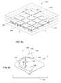
- Spatial light modulator 110comprises an array of micromirrors that has m ⁇ n micromirrors (e.g. micromirror device 114 ), wherein m and n respectively represent the number of micromirror devices in a row and a column of the array.
- the micromirror arrayalso has a well defined diagonal, which is generally measured in inches.
- a gap and pitchis defined by two adjacent micromirrors.
- L platemeasures the size of the micromirror
- W postmeasures the post area of the micromirror.
- the post areais the area in which posts (e.g. post 219 in FIG. 8 b and FIG.
- the insert figureillustrates the dimensions of the micromirror and the adjacent micromirrors with the micromirror of rectangular shape, those dimension definitions are applicable to any micromirrors and micromirror arrays.
- an optimum diameteris determined for the micromirror array of the spatial light modulator.
- the brightness of images produced by the spatial light modulator modulating light from the arc lampthe cost of spatial light modulator and value (defined as the brightness per cost) versus the overall diameter of the spatial light modulator are illustratively plotted in FIG. 3 .
- brightness and costare respectively plotted in dash-line and dotted-line with reference to the Y axis on the right side.
- the valueis plotted in solid-line with reference to Y axis on the left side.
- brightnessincreases with the diameter of the micromirror array increasing and saturates after the diameter of the micromirror array is around 0.8 inch.
- the costis linearly proportional to the diameter of the micromirror array.
- the value, defined as the brightness per costvaries with the diameter of the micromirror array and presents a maximum value when the diameter is around 0.7 inch.
- the diameter of the micromirror arrayis preferably from 0.55 inch to 0.8 inch, more preferably from 0.65 to 0.75 inch, and more preferably around 0.7 inch.
- FIG. 4illustrates the variation of the pitch versus diameter of the micromirror array at different resolutions. Referring to FIG. 4 , open circles, open squares, open triangles and solid circles respectively represents resolutions of 1280 ⁇ 720, 1400 ⁇ 1050, 1600 ⁇ 1200 and 1920 ⁇ 1080.
- the optimum pitch sizesare from 4.38 to 6.57 ⁇ m with the resolution varying from 1920 ⁇ 1080 to 1280 ⁇ 720.
- the optimum pitch sizesare from 6.23 to 9.34 ⁇ m with the resolution varying from 1920 ⁇ 1080 to 1280 ⁇ 720.
- the optimum pitch sizesare from 8.07 to 12.11 ⁇ m with the resolution varying from 1920 ⁇ 1080 to 1280 ⁇ 720.
- the optimum pitch sizesare from 9.92 to 14.87 ⁇ m with the resolution varying from 1920 ⁇ 1080 to 1280 ⁇ 720.
- the diameter of the micromirror arraydepends upon two dimensional parameters—the diagonal of the mirror plate (L plate ) of the micromirror and the gap between adjacent micromirrors, as defined in FIG. 2 .
- the gapdegrades the optical efficiency of the micromirror in reflecting light.
- This type of degradationcan be analyzed in terms of illumination efficiency, which is defined as the ratio of the total effective reflective area to the total area of the micromirror array.
- the pitch size of the micromirror arrayis at least 4.38 ⁇ m so as to obtain the illumination efficiency higher than 85%.
- the pitch size of the micromirror arrayis at least 8.07 ⁇ m so as to obtain the illumination efficiency higher than 85%. If the illumination efficiency is desired to be higher than 90%, the pitch size is at least 4.38 ⁇ m, 6.23 ⁇ m and 10.16 ⁇ m when the gap size is around 0.15 ⁇ m, 0.25 ⁇ m and 0.5 ⁇ m, respectively.
- the pitch size of the micromirror array deviceis preferably from 4.38 ⁇ m to 10.16 ⁇ m, preferably from 4.38 ⁇ m to 9.341 ⁇ m, and preferably from 4.38 ⁇ m to 6.57 ⁇ m, and preferably from 6.231 ⁇ m to 9.34 ⁇ m, and more preferably from 8.07 ⁇ m to 10.16 ⁇ m. It is also preferred that the gap between adjacent micromirrors is 0.5 ⁇ m or less, more preferably, from 0.25 ⁇ m to 0.5 ⁇ m, and more preferably from 0.15 ⁇ m to 0.25 ⁇ m.
- the micromirror array within the spatial light modulator of the display systemhas an optimum diameter.
- the pitchis a summation of the length of the micromirror and the gap between adjacent micromirrors
- the reduction of the pitchcan be achieved by either reducing the micromirror size or the gap between adjacent micromirrors. Reduction of the micromirror size without reducing the gap size, however, damages the illumination efficiency of the micromirror array, as discussed with reference to FIG. 5 .
- reduction of the gapis also preferred in achieving higher resolution for a micromirror array with the given optimum diameter.
- reduction of the pitchcan be achieved by reducing the gap size and the mirror size, the gap size and the mirror size do not have to both be reduced.
- reduction of the gapis preferred to achieve a small pitch if it is achievable. If the desired small pitch is not achievable by reducing the gap only, mirror size is reduced.
- the micromirror of the present inventionis designed such that the mirror plate of the micromirror rotates asymmetrically along a rotation axis, because asymmetric rotation allows for a smaller gap than the symmetric rotation.
- the distance between the mirror plate and the rotation axisis as small as compared to the distance between the mirror plate and the substrate on which the mirror plate is formed.
- FIG. 6 a , FIG. 6 b and FIG. 6 cAs an optional feature of the invention, such asymmetry aids in achieving smaller pitch and gap micromirror arrays without adjacent micromirrors impacting each other.
- FIG. 6 aillustrates a cross-sectional view of two adjacent micromirrors, each rotating symmetrically.
- the solid dark circle in each micromirrorrepresents the rotation axis of the mirror plate.
- Pitch 1measures the pitch (equal to the distance between the two rotation axes) between the adjacent micromirrors.
- t sacis the distance between the mirror plate and the rotation axis.
- the trajectory of the ends of each mirror plateis plotted in dotted circle.
- the micromirror 2is fixed and its mirror plate is rotated clockwise to the OFF state angle corresponding to the OFF state of the micromirror.
- the micromirror 1can be fabricated to be closer or further away from micromirror 2 . And the pitch 1 is thus variable.
- the micromirror 1is placed at a position such that during the counter-clockwise rotation of the mirror plate of the micromirror 1 towards the ON state angle, the “right” end of the mirror plate is tangent but without impacting to the “left” end of the mirror plate of the micromirror 2 . From this situation, gap 1 is defined by the two mirror plates of the two adjacent micromirrors when they are “flat” (e.g. parallel to the substrate or non-deflected).
- FIG. 6 billustrates a cross-sectional view of two adjacent micromirrors, each rotating symmetrically, while the distance t sac2 between the mirror plate and the rotation axis is smaller than that in FIG. 6 a , that is t sac2 ⁇ t sac1 .
- FIG. 6 ca cross-sectional view of two adjacent micromirrors, each being attached to the hinge such that he mirror plate rotates asymmetrically along the rotation axis, is illustrated therein. Specifically, each mirror plate is attached to the hinge, and the attachment point is positioned closer to one end of the mirror plate than the other. For example, the attachment point of the mirror plate of the micromirror 1 is positioned away from the “right” end A of the mirror plate.
- the attachment point of the mirror plate of the micromirror 2is positioned towards the “left” end B of the micromirror 2 .
- the mirror platesare otherwise identical to those in FIG. 6 a and FIG. 6 b (e.g. the distance between the mirror plate and the rotation axis in FIG. 6 c is the same as that in FIG. 6 b ).
- the trajectories of the end A and end B of the mirror platesare plotted in dotted circles. Because the rotations of the mirror plates along their rotation axes are asymmetrical, the trajectory circles of the end A and end B are different.
- FIG. 6 care smaller than those in FIG. 6 b and FIG. 6 a .
- a small distance between the mirror plate and the rotation axis and an asymmetric rotationare not required in the present invention, they aid in the ability to achieve small pitch and small gap micromirror arrays—particularly at the lower ends of the dimension ranges in the present invention.
- FIG. 7a cross-sectional view of two adjacent micromirrors is illustrated therein.
- the mirror plates (e.g. mirror plate 116 ) of the micromirrorseach rotates asymmetrically along a rotation axis.
- the mirror platee.g. mirror plate 116
- a hingee.g. hinge 120
- a hinge contacte.g. hinge contact 118
- the distance between the mirror plate and the hingeis denoted by t sac .
- the mirror plateis attached to the hinge asymmetrically.
- the attachment point of the mirror plate to the hinge contactis extended towards one end of the mirror plate so as to enabling the mirror plate to rotate asymmetrically to an ON state or an OFF state.
- the ON stateis defined as a state wherein light reflected by the mirror plate is collected by the projection lens (e.g. projection lens 108 in FIG. 1 ) and generating a “bright” pixel of an image on the display target (e.g. display target 112 in FIG. 1 ).
- the OFF stateis defined as a state wherein light is reflected by the mirror plate away from the projection lens—resulting in a “dark” pixel on the display target.
- the ON state angle and the OFF state angleaffect the quality of the produced image, such as the contrast ratio of the image.
- a large ON state angle corresponding to the ON state and a non-zero OFF state angle corresponding to the OFF stateare preferred.
- the ON state angleis from 12° degrees to 18° degrees
- the OFF state angleis from ⁇ 2° degrees to ⁇ 8° degrees, wherein the “+” and “ ⁇ ” signs represent opposite rotation directions of the mirror plate as shown in the figure.
- the ON state rotation angle and the OFF state rotation angleare achieved by applying an electrostatic force to the mirror plate and providing stop mechanisms for stopping the rotation of the mirror plates when the mirror plate rotates to the ON state angle or the OFF state angle.
- the stop mechanismcan be a substrate (e.g. substrate 210 in FIG. 8 b ) on which the mirror plate is formed or designated stops (e.g. stop 216 in FIG. 8 b ).
- a small distance between the mirror plate and the hingeis desired to benefit large rotation angle for the ON state and a small rotation angle for the OFF state.
- the distance between the mirror plate and the hingeis preferably from 0.15 to 0.45 micrometers, e.g.
- the mirror plate and the hingecould also be used, such as a distance from 0.5 to 1.5 micrometers, or from 0.5 to 0.8 micrometers, or from 0.8 to 1.25 micrometers, or from 1.25 to 1.5 micrometers.
- the micromirror array devicecomprises m ⁇ n micromirrors, wherein m and n respectively represents the number of micromirrors in a row and the number of micromirrors in a column of the array.
- the values of m and ndetermine the resolution of the displayed images.
- the m ⁇ nare preferably 1280 ⁇ 720, 1400 ⁇ 1050, 1600 ⁇ 1200, 1920 ⁇ 1080, 2048 ⁇ 1536 or higher.
- Adjacent micromirrors in a row or a column of the micromirror arraydefine a gap therebetween.
- the gapdetermines the fill factor of the micromirror array device, wherein the fill factor is defined as the ratio of the total area of the mirror plates of the micromirrors to the area of the micromirror array.
- the fill factorcan be calculated by: the area of a micromirror plate of the micromirror divided by the pitch squared, provided that the mirror plates of the micromirrors are identical and the pitch size is uniform over the entire micromirror array.
- the fill factor of the micromirror array deviceis 85% or higher, and more preferably, 90% or higher.
- electrode array 225is disposed for selectively actuating the micromirrors.
- an electrostatic fieldis established between the selected micromirror and the electrode disposed proximate to and designated for rotating the selected micromirror.
- the micromirrorrotates relative to substrate 210 to either an ON state or an OFF state (if the OFF state is defined as the micromirror having an angle with substrate 210 ) such that light incident onto the selected micromirror through substrate 210 can be reflected either into or away from a projection lens (e.g. projection lens 108 in FIG. 1 a ).
- a projection lense.g. projection lens 108 in FIG. 1 a
- the micromirrorsare formed on substrate 210 , such as quartz or glass that is transmissive to visible light.
- the electrode arrayis formed on substrate 215 , which is a standard semiconductor wafer.
- a circuit arraysuch as a DRAM or SRAM array is also formed on substrate 215 .
- Each circuitmaintains a voltage signal and is connected to one electrode such that the voltage of the electrode is defined by the voltage signal in the circuitry. In this way, the electrostatic field between the mirror plate and the electrode is controlled by the circuit.
- FIG. 8 bschematically illustrates a back-view of a micromirror of micromirror array 110 .
- the micromirrorcomprises mirror plate 212 , hinge 222 , hinge contact 224 and hinge support 218 .
- the mirror plateis connected to the hinge through the contact.
- the hingeis affixed to the hinge support that is formed on substrate 210 . It is noted that the mirror plate is attached to the hinge such that the mirror plate can rotate relative to the substrate along a rotation axis that is parallel to but offset from a diagonal of the mirror plate when viewed from the top of the substrate.
- the axis of rotationcan be exactly parallel to or substantially parallel to ( ⁇ 19 degrees) the diagonal of the micromirror but offset from the diagonal when viewed from the above.
- the mirror plateis able to rotate asymmetrically along the rotation axis in two opposite rotation directions and achieves a large ON state angle compared to the ON state angles achieved by those micromirrors rotating symmetrically.
- the ON state angleis preferably +12° degrees or more, preferably +16° degrees or more, preferably +18° degrees or more and more preferably +20° degrees or more.
- the OFF state angleis preferably from ⁇ 10 degree to ⁇ 80 degrees, and preferably around ⁇ 40 degrees.
- stops 216 and 217can be formed on the hinge support for stopping rotations of the mirror plate when the mirror plate achieves the ON state and OFF state angles.
- stop 216 and stop 217are respectively designated for stopping the mirror plate in rotating in a direction towards the ON state and in another direction towards the OFF state.
- the mirror platerotates in response to an electrostatic field between the mirror plate and the electrode associated with the mirror plate.
- an electrodeis associated with the mirror plate for driving the mirror plate to rotate to the ON state.
- a separate electrode(not shown) can be provided.
- the second electrodecan be placed in any suitable location as along as it drives the mirror plate to rotate to the non-zero OFF state angle.
- the second electrodecan be placed on the same substrate as the first electrode for the ON state is disposed, but at a location on the opposite side of the rotation axis of the mirror plate.
- the second electrodecan be disposed on the opposite side of the mirror plate in relation to the first electrode for the ON state.
- the second electrodecan be formed on the glass substrate, on which the micromirrors are formed.
- the second electrodeis preferably an electrode grid, or electrode frame (or segments, such as stripes) below each micromirror.
- the second electrodecan also be formed as an electrode film on the surface of the glass substrate, in which case, the electrode film is transparent to visible light.
- the second electrode on the glass substratecan also be used as light absorbing grid (or frame or segments) or anti-reflection film.
- the OFF state corresponding to the non-zero OFF state anglecan be achieved without the second electrode.
- a portion of the hinge structurecan be made such that the portion is curved away from parallel to the substrate at the natural resting state.
- the mirror plate, which is attached to the curved portionpresent an angle to the substrate at the natural resting state.
- FIG. 9 a and FIG. 9 banother exemplary micromirror array device and micromirror are illustrated therein.
- the shape of the mirror plate, shape of the hinge structure and relative arrangement of the mirror plate and the hinge structure of the micromirrorare different from those in FIG. 8 .
- the micromirror and the micromirror array of the micromirror array devicecan take many suitable forms.
- the micromirrors and the electrodes of the micromirror array devicecan be formed on the same substrate (e.g. substrate 210 in FIG. 9 a ).
- more than one electrodecan be disposed proximate to each micromirror for rotating the mirror plate of the micromirror.
- at least one electrodeis designated for driving the mirror plate to rotate in a first rotational direction
- at least another electrodeis designated for driving the mirror plate to rotate in a second rotational direction that is opposite to the first rotation direction.
- micromirror devicethere is a variety of ways to construct the micromirror device described above, such as the fabrication methods disclosed in U.S. Pat. Nos. 5,835,256 and 6,046,840 both to Huibers, the subject matter of each being incorporated herein by reference.
- sacrificial materialsare deposited between structures of the micromirrors and removed afterwards.
- a sacrificial materialis deposited between the mirror plate and the hinge to which the mirror plate is attached.
- the order of the fabrication steps for the mirror plate and the hingedepends upon the selected fabrication process and other factors, such as substrate.
- the mirror platecan be fabricated before the hinge, and alternatively, it can be fabricated after the hinge.
- the hingeis fabricated before the mirror plate on the silicon wafer.
- the mirror plateis then fabricated before fabricating the hinge on the glass substrate.
- the sacrificial materialalso fills the space, such as gaps between adjacent micromirrors of the micromirror array. Removal of those sacrificial materials, however, is not a trivial process.
- the size of the gap between the hinge and the mirror plateis preferably from 0.15 to 0.45 microns, although the distance between the mirror plate and the hinge can be 0.15 to 1.5 microns according to the present invention.
- a spontaneous vapor phase chemical etching processis employed, which will be described in the following discussion on an exemplary fabrication process.
- FIG. 10 a through FIG. 10 cA demonstrative fabrication process for making the micromirror and the micromirror array device of the present invention will be discussed in the following with references to FIG. 10 a through FIG. 10 c .
- U.S. patent application Ser. No. 09/910,537 filed on Jul. 20, 2001 and 60/300,533 filed on Jun. 22, 2001 both to Reidcontain examples of the materials that may be used for the various components of the present invention. These patent applications are also incorporated herein by reference. It should be appreciated by those of ordinary skill in the art that the exemplary processes are for demonstration purpose only and should not be interpreted as limitations.
- the exemplary micromirroris formed on a glass substrate that is transparent to visible light.
- electrode and circuitryare formed on a separate substrate, such as a silicon wafer.
- the micromirror and the electrode and circuitrycan be formed on the same substrate.
- FIG. 10 aa cross-section view of a micromirror FIG. 8 b during an exemplary fabrication process is illustrated therein.
- the micromirroris formed on substrate 210 , which can be glass (e.g. 1737F, Eagle 2000, quartz, PyrexTM, sapphire) that is transparent to visible light.
- First sacrificial layer 240is deposited on substrate 210 followed by forming mirror plate 232 .
- First sacrificial layer 240may be any suitable material, such as amorphous silicon, or could alternatively be a polymer or polyimide, or even polysilicon, silicon nitride, silicon dioxide and tungsten, depending upon the choice of sacrificial materials, and the etchant selected.
- the first sacrificial layeris amorphous silicon, and it is preferably deposited at 300–350° C.
- the thickness of the first sacrificial layercan be wide ranging depending upon the micromirror size and desired title angle of the micro-micromirror, though a thickness of from 500 ⁇ to 50,000 ⁇ , preferably close to 25,000 ⁇ , is preferred.
- the first sacrificial layermay be deposited on the substrate using any suitable method, such as LPCVD or PECVD.
- an anti-reflection filmmaybe deposited on the surface of substrate 210 .
- the anti-reflection filmis deposited for reducing the reflection of the incident light from the surface of the substrate.
- other optical enhancing filmsmay be deposited on either surface of the glass substrate as desired.
- an electrodemay be formed on a surface of substrate 210 .
- the electrodecan be formed as an electrode grid or a series of electrode segments (e.g. electrode strips) around the mirror plate.
- the electrodecan be formed as an electrode film on the surface of substrate 210 , in which case, the electrode film is transparent to visible light.
- the electrodecan be used for driving the mirror plate to either the ON state or the OFF state.
- a light absorbing gridcan be deposited on a surface of the glass substrate and around or below each micromirror.
- the light absorbing frameabsorbs light incident onto and/or scattered light from the edges of the micromirrors. The absorption of the scattered light improves the quality of performance, such as contrast ratio, of the micromirror.
- mirror plate 232is deposited and patterned on the first sacrificial layer.
- the micromirroris designated for reflecting incident light in the spectrum of interest (e.g. visible light spectrum)
- the micromirror plate layercomprises of one or more materials that exhibit high reflectivity (preferably 90% or higher) to the incident light.
- the thickness of the micromirror platecan be wide ranging depending upon the desired mechanical (e.g. elastic module), the size of the micromirror, desired ON state angle and OFF state angle, and electronic (e.g. conductivity) properties of the mirror plate and the properties of the materials selected for forming the micromirror plate.
- mirror plate 232is a multi-layered structure, which comprises a SiO x layer with a preferred thickness around 400 ⁇ , a light reflecting layer of aluminum with a preferred thickness around 2500 ⁇ , a titanium layer with a preferred thickness around 80 ⁇ , and a 200 ⁇ TiN x layer.
- a SiO x layerwith a preferred thickness around 400 ⁇
- a light reflecting layer of aluminumwith a preferred thickness around 2500 ⁇
- titanium layerwith a preferred thickness around 80 ⁇
- a 200 ⁇ TiN x layerIn addition to aluminum, other materials, such as Ti, AlSiCu and TiAl, having high reflectivity to visible light can also be used for the light reflecting layer.
- These mirror plate layerscan be deposited by PVD at a temperature preferably around 150° C.
- mirror plate 232is patterned into a desired shape, such as that in FIG. 8 b or FIG. 9 b .
- the patterning of the micromirrorcan be achieved using standard photoresist patterning followed by etching using, for example CF4, Cl2, or other suitable etchant depending upon the specific material of the micromirror plate layer.
- second sacrificial layer 242is deposited on the mirror plate 232 and first sacrificial layer 240 .
- the second sacrificial layermay comprise amorphous silicon, or could alternatively comprise one or more of the various materials mentioned above in reference to the first sacrificial layer.
- First and second sacrificial layersneed not be the same, although they are the same in the preferred embodiment so that, in the future, the etching process for removing these sacrificial materials can be simplified.
- the second sacrificial layermay be deposited using any suitable method, such as LPCVD or PECVD.
- the second sacrificial layercomprises amorphous silicon deposited at approximate 350° C.
- the thickness of the second sacrificial layercan be on the order of 12,000 ⁇ , but may be adjusted to any reasonable thickness, such as between 2,000 ⁇ and 20,000 ⁇ depending upon the desired distance (in the direction perpendicular to the micromirror plate and the substrate) between the micromirror plate and the hinge. It is preferred that the hinge and mirror plate be separated by a gap with a size from 0.1 to 1.5 microns, more preferably from 0.1 to 0.45 micron, and more preferably from 0.25 to 0.45 microns. Larger gaps could also be used, such as a gap from 0.5 to 1.5 micrometers, or from 0.5 to 0.8 micrometer, or from 0.8 to 1.25 micrometers, or from 1.25 to 1.5 micrometers.
- the micromirror platecomprises aluminum, and the sacrificial layers (e.g. the first and second sacrificial layer) are amorphous silicon.
- the sacrificial layerse.g. the first and second sacrificial layer
- a protection layermaybe deposited on the patterned micromirror plate before depositing the second sacrificial silicon layer such that the aluminum layer can be isolated from the silicon sacrificial layer. This protection may or may not be removed after removing the sacrificial materials. If the protection layer is not to be removed, it is patterned after deposition on the mirror plate.
- the deposited second sacrificial layeris then patterned for forming two deep-via areas 248 and shallow via area 246 using standard lithography technique followed by etching, as shown in the figure.
- the etching stepmay be performed using Cl 2 , BCl 3 , or other suitable etchant depending upon the specific material(s) of the second sacrificial layer.
- the distance across the two deep-via areasdepends upon the length of the defined diagonal of the micromirror plate. In an embodiment of the invention, the distance across the two deep-via areas after the patterning is preferably around 10 ⁇ m, but can be any suitable distance as desired.
- an etching step using CF 4 or other suitable etchantmay be executed.
- the shallow-via areawhich can be of any suitable size, is preferably on the order of 2.2 square microns. And the size of each deep-via is approximate 1.0 micron.
- hinge structure layer 250is deposited on the patterned second sacrificial layer. Because the hinge structure is designated for holding the hinge (e.g. hinge 222 in FIG. 8 b ) and the micromirror plate (e.g. mirror plate 232 in FIG. 8 b ), it is desired that the hinge structure layer comprises of materials having at least large elastic modulus.
- hinge structure layer 250comprises a 400 ⁇ thickness of TiN x (although it may comprise TiN x , and may have a thickness between 100 ⁇ and 2000 ⁇ ) layer deposited by PVD, and a 3500 ⁇ thickness of SiN x (although the thickness of the SiN x layer may be between 2000 ⁇ and 10,000 ⁇ ) layer 350 deposited by PECVD.
- TiN x layeris not necessary for the invention, but provides a conductive contact surface between the micromirror and the hinge in order to, at least, reduce charge-induced stiction.
- hinge structure layer 250is patterned into a desired configuration, such as hinge structure 218 in FIG. 8 b .
- An etching step using one or more proper etchantsis executed in patterning the hinge structure layer.
- the layercan be etched with a chlorine chemistry or a fluorine chemistry where the etchant is a perfluorocarbon or hydrofluorocarbon (or SF 6 ) that is energized so as to selectively etch the hinge support layers both chemically and physically (e.g. a plasma/RIE etch with CF 4 , CHF 3 , C 3 F 8 , CH 2 F 2 , C 2 F 6 , SF 6 , etc.
- each hinge support layere.g. chlorine chemistry for a metal layer, hydrocarbon or fluorocarbon (or SF 6 ) plasma for silicon or silicon compound layers, etc.
- the bottom segment of contact area 236is removed and part of the micromirror plate underneath the contact area is thus exposed to hinge layer 238 , which is deposited on the patterned hinge structure layer, to form an electric-contact with external electric source.
- the sidewalls of contact area 236are left with residues of the hinge structure layers after patterning. The residue on the sidewalls helps to enhance the mechanical and electrical properties of the hinge.
- Each of the two deep-via areas 234 on either side of the mirrorcan form a continuous element with the deep-via areas corresponding to the adjacent micromirror in an array.
- the hinge layeris also used as an electric contact for the micromirror plate. It is desired that the material of the hinge layer is electrically conductive. Examples of suitable materials for the hinge layer are silicon nitride, silicon oxide, silicon carbide, polysilicon, Al, Ir, titanium, titanium nitride, titanium oxide(s), titanium carbide, CoSiN x , TiSiN x , TaSiN x , or other ternary and higher compounds. When titanium is selected for the hinge layer, it can be deposited at 100° C. Alternatively, the hinge layer may comprise of multi-layers, such as 100 ⁇ TiN x and 400 ⁇ SiN x .
- the hinge layeris then patterned as desired using etching. Similar to the hinge structure layer, the hinge layer can be etched with a chlorine chemistry or a fluorine chemistry where the etchant is a perfluorocarbon or hydrofluorocarbon (or SF 6 ) that is energized so as to selectively etch the hinge layers both chemically and physically (e.g. a plasma/RIE etch with CF 4 , CHF 3 , C 3 F 8 , CH 2 F 2 , C 2 F 6 , SF 6 , etc.
- etchantsmay, of course, be employed for etching each hinge layer (e.g. chlorine chemistry for a metal layer, hydrocarbon or fluorocarbon (or SF 6 ) plasma for silicon or silicon compound layers, etc.).
- the micromirroris released by removing the sacrificial materials of the first and second sacrificial layers, which will be discussed in detail in the following with reference to FIG. 11 and FIG. 12 .
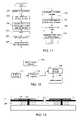
- a cross-sectional view of the released micromirror deviceis presented in FIG. 10 c.
- the release etchingutilizes an etchant gas capable of spontaneous chemical etching of the sacrificial material, preferably isotropic etching that chemically (and not physically) removes the sacrificial material.
- an etchant gascapable of spontaneous chemical etching of the sacrificial material, preferably isotropic etching that chemically (and not physically) removes the sacrificial material.
- Preferred etchants for the release etchare gas phase fluoride etchants that, except for the optional application of temperature, are not energized. Examples include HF gas, noble gas halides such as xenon difluoride, and interhalogens such as IF 5 , BrCl 3 , BrF 3 , IF 7 and ClF 3 .
- the release etchmay comprise inner gas components such as (N 2 , Ar, Xe, He, etc.). In this way, the remaining sacrificial material is removed and the micromechanical structure is released.
- XeF 2is provided in an etching chamber with diluents (e.g. N 2 and He).
- the concentration of XeF 2is preferably 8 Torr, although the concentration can be varied from 1 Torr to 30 Torr or higher.
- This non-plasma etchis employed for preferably 900 seconds, although the time can vary from 60 to 5000 seconds, depending on temperature, etchant concentration, pressure, quantity of sacrificial material to be removed, or other factors.
- the etch ratemay be held constant at 18 ⁇ /s/Torr, although the etch rate may vary from 1 ⁇ /s/Torr to 100 ⁇ /s/Torr.
- Each step of the release processcan be performed at room temperature.
- etchants and etching methodsfor use in either the final release or in an intermediate etching step, there are others that may also be used by themselves or in combination. Some of these include wet etches, such as ACT, KOH, TMAH, HF (liquid); oxygen plasma, SCCO 2 , or super critical CO 2 (the use of super critical CO 2 as an etchant is described in U.S. patent application Ser. No. 10/167,272, which is incorporated herein by reference).
- spontaneous vapor phase chemical etchantsare more preferred, because the sacrificial material, such as amorphous silicon within small spaces, (such as lateral gap 242 (between the mirror plate and the hinge) and small gap 240 (between the substrate and the mirror plate) in FIG. 13 ) can be efficiently removed via gaps between adjacent mirror plates and the lateral gap as compared to other sacrificial materials (e.g. organic materials) and other etching methods.
- a micromirror array with a small gap, a small pitch and a small distance between the hinge and the mirror platecan thus be more easily fabricated with such spontaneous vapor phase chemical etchants.
- a flow chartshows the steps executed in an exemplary etching process for removing the sacrificial material (amorphous silicon).
- the etching processstarts at a breakthrough etching (step 254 ) in breakthrough etching chamber ( 272 in FIG. 12 ) of an etching system for removing the oxidation layers on the surfaces of the micromirror.
- This etching stepmay lasts for tens of seconds.
- the micromirroris breakthrough etched around 30 seconds.
- the micromirroris then loaded into the etching chamber (e.g. 278 in FIG. 12 ) of the etching system for etching the sacrificial materials.
- One or more vapor phase etchantsare prepared (step 258 ) in the building chamber (e.g. 274 in FIG. 12 ) for vaporizing the etchants and the expansion chamber (e.g. 276 in FIG. 12 ) for setting the vapor phase etchants to a certain pressure.
- the expanded vapor phase etchantsare then pumped into (step 258 ) the etching chamber (e.g. etching chamber 278 in FIG. 12 ).
- the micromirroris then etched in the etching chamber for a time preferably around 1200 seconds so as to thoroughly remove the sacrificial materials.
- the etching of the micromirror in the etching chambermay be performed with an end-point detection technique for real-timely monitoring the etching process in the etching chamber.
- a residual gas analyzerwhich analyzes the gas from the etching chamber, is preferably used.
- the residual gas analyzermeasures the chemical components and the density of certain component (it can also measure the density variation rate of the certain component) of the gas from the etching chamber. From the measurements, the amount of sacrificial material inside the etching chamber may be derived. With the end-point detection, over-etching and incomplete etching may be avoided.
- the etching chamberis cleaned by pumping out the gases inside the etching chamber (step 262 ).
- the etched micromirroris then unloaded from the etching chamber (step 264 ).
- the micromirror after etchingis coated with a self-assembled-monolayer (SAM) for protecting the micromirror (e.g. from a trichlorosilane or trialkanesilane precursors).
- SAMself-assembled-monolayer
- the micromirroris loaded into the SAM chamber (e.g. SAM chamber 280 in FIG. 12 ) (step 264 ).
- the SAM materialis then pumped into the SAM chamber (step 266 ).
- the micromirror inside the SAM chamberis exposed to the SAM material for around 60 seconds, and coated with the SAM materials thereby.
- the micromirroris unloaded from the SAM chamber (step 270 ).
- PVD and CVDare referred to above, other thin film deposition methods could be used for depositing the layers, including spin-on, sputtering, anodization, oxidation, electroplating and evaporation. Therefore, the invention as described herein contemplates all such embodiments as may come within the scope of the following claims and equivalents thereof.
Landscapes
- Physics & Mathematics (AREA)
- Engineering & Computer Science (AREA)
- Chemical & Material Sciences (AREA)
- General Physics & Mathematics (AREA)
- Optics & Photonics (AREA)
- Nanotechnology (AREA)
- Signal Processing (AREA)
- Multimedia (AREA)
- Composite Materials (AREA)
- Condensed Matter Physics & Semiconductors (AREA)
- Materials Engineering (AREA)
- Crystallography & Structural Chemistry (AREA)
- Mechanical Light Control Or Optical Switches (AREA)
- Projection Apparatus (AREA)
- Micromachines (AREA)
Abstract
Description
wherein the term (pitch-gap)2−2×Wpost2is the total effective reflection area of the micromirrors of the micromirror array, and pitch2is the total area of the micromirrors of the micromirror array.
Claims (52)
Priority Applications (1)
| Application Number | Priority Date | Filing Date | Title |
|---|---|---|---|
| US11/034,398US6970281B2 (en) | 2003-07-03 | 2005-01-11 | Micromirror array having reduced gap between adjacent micromirrors of the micromirror array |
Applications Claiming Priority (3)
| Application Number | Priority Date | Filing Date | Title |
|---|---|---|---|
| US10/613,379US6873450B2 (en) | 2000-08-11 | 2003-07-03 | Micromirrors with mechanisms for enhancing coupling of the micromirrors with electrostatic fields |
| US10/627,302US6965468B2 (en) | 2003-07-03 | 2003-07-24 | Micromirror array having reduced gap between adjacent micromirrors of the micromirror array |
| US11/034,398US6970281B2 (en) | 2003-07-03 | 2005-01-11 | Micromirror array having reduced gap between adjacent micromirrors of the micromirror array |
Related Parent Applications (1)
| Application Number | Title | Priority Date | Filing Date |
|---|---|---|---|
| US10/627,302ContinuationUS6965468B2 (en) | 2002-03-22 | 2003-07-24 | Micromirror array having reduced gap between adjacent micromirrors of the micromirror array |
Publications (2)
| Publication Number | Publication Date |
|---|---|
| US20050231788A1 US20050231788A1 (en) | 2005-10-20 |
| US6970281B2true US6970281B2 (en) | 2005-11-29 |
Family
ID=34080615
Family Applications (5)
| Application Number | Title | Priority Date | Filing Date |
|---|---|---|---|
| US10/627,302Expired - LifetimeUS6965468B2 (en) | 2002-03-22 | 2003-07-24 | Micromirror array having reduced gap between adjacent micromirrors of the micromirror array |
| US11/034,294Expired - LifetimeUS7002726B2 (en) | 2003-07-24 | 2005-01-11 | Micromirror having reduced space between hinge and mirror plate of the micromirror |
| US11/034,399Expired - LifetimeUS6972891B2 (en) | 2003-07-24 | 2005-01-11 | Micromirror having reduced space between hinge and mirror plate of the micromirror |
| US11/034,318Expired - LifetimeUS6985277B2 (en) | 2003-07-03 | 2005-01-11 | Micromirror array having reduced gap between adjacent micromirrors of the micromirror array |
| US11/034,398Expired - LifetimeUS6970281B2 (en) | 2003-07-03 | 2005-01-11 | Micromirror array having reduced gap between adjacent micromirrors of the micromirror array |
Family Applications Before (4)
| Application Number | Title | Priority Date | Filing Date |
|---|---|---|---|
| US10/627,302Expired - LifetimeUS6965468B2 (en) | 2002-03-22 | 2003-07-24 | Micromirror array having reduced gap between adjacent micromirrors of the micromirror array |
| US11/034,294Expired - LifetimeUS7002726B2 (en) | 2003-07-24 | 2005-01-11 | Micromirror having reduced space between hinge and mirror plate of the micromirror |
| US11/034,399Expired - LifetimeUS6972891B2 (en) | 2003-07-24 | 2005-01-11 | Micromirror having reduced space between hinge and mirror plate of the micromirror |
| US11/034,318Expired - LifetimeUS6985277B2 (en) | 2003-07-03 | 2005-01-11 | Micromirror array having reduced gap between adjacent micromirrors of the micromirror array |
Country Status (5)
| Country | Link |
|---|---|
| US (5) | US6965468B2 (en) |
| JP (1) | JP2006528794A (en) |
| KR (1) | KR20060065647A (en) |
| CN (1) | CN1856726A (en) |
| WO (1) | WO2005049481A2 (en) |
Cited By (6)
| Publication number | Priority date | Publication date | Assignee | Title |
|---|---|---|---|---|
| US20050196896A1 (en)* | 2003-05-13 | 2005-09-08 | Satyadev Patel | Micromirror array device |
| US20080151345A1 (en)* | 2006-12-26 | 2008-06-26 | Zhou Tiansheng | Micro-electro-mechanical-system micromirrors for high fill factor arrays and method therefore |
| US20100302617A1 (en)* | 2009-06-01 | 2010-12-02 | Zhou Tiansheng | Mems micromirror and micromirror array |
| US9036231B2 (en) | 2010-10-20 | 2015-05-19 | Tiansheng ZHOU | Micro-electro-mechanical systems micromirrors and micromirror arrays |
| US9385634B2 (en) | 2012-01-26 | 2016-07-05 | Tiansheng ZHOU | Rotational type of MEMS electrostatic actuator |
| US10551613B2 (en) | 2010-10-20 | 2020-02-04 | Tiansheng ZHOU | Micro-electro-mechanical systems micromirrors and micromirror arrays |
Families Citing this family (142)
| Publication number | Priority date | Publication date | Assignee | Title |
|---|---|---|---|---|
| US6674562B1 (en)* | 1994-05-05 | 2004-01-06 | Iridigm Display Corporation | Interferometric modulation of radiation |
| US7907319B2 (en)* | 1995-11-06 | 2011-03-15 | Qualcomm Mems Technologies, Inc. | Method and device for modulating light with optical compensation |
| WO2003007049A1 (en)* | 1999-10-05 | 2003-01-23 | Iridigm Display Corporation | Photonic mems and structures |
| US7019376B2 (en)* | 2000-08-11 | 2006-03-28 | Reflectivity, Inc | Micromirror array device with a small pitch size |
| US7006275B2 (en)* | 2000-08-30 | 2006-02-28 | Reflectivity, Inc | Packaged micromirror array for a projection display |
| US6958123B2 (en)* | 2001-06-15 | 2005-10-25 | Reflectivity, Inc | Method for removing a sacrificial material with a compressed fluid |
| US6965468B2 (en)* | 2003-07-03 | 2005-11-15 | Reflectivity, Inc | Micromirror array having reduced gap between adjacent micromirrors of the micromirror array |
| TWI289708B (en)* | 2002-12-25 | 2007-11-11 | Qualcomm Mems Technologies Inc | Optical interference type color display |
| TW570896B (en) | 2003-05-26 | 2004-01-11 | Prime View Int Co Ltd | A method for fabricating an interference display cell |
| US7209321B1 (en) | 2003-07-31 | 2007-04-24 | Western Digital Technologies, Inc. | Disk drive pulse width modulating a voice coil motor using model reference current feedback |
| US7643195B2 (en)* | 2003-11-01 | 2010-01-05 | Silicon Quest Kabushiki-Kaisha | Mirror device |
| US20080088651A1 (en)* | 2003-11-01 | 2008-04-17 | Yoshihiro Maeda | Divided mirror pixels for deformable mirror device |
| US7342705B2 (en)* | 2004-02-03 | 2008-03-11 | Idc, Llc | Spatial light modulator with integrated optical compensation structure |
| US7706050B2 (en)* | 2004-03-05 | 2010-04-27 | Qualcomm Mems Technologies, Inc. | Integrated modulator illumination |
| US7855824B2 (en)* | 2004-03-06 | 2010-12-21 | Qualcomm Mems Technologies, Inc. | Method and system for color optimization in a display |
| US7068417B2 (en)* | 2004-07-28 | 2006-06-27 | Miradia Inc. | Method and apparatus for a reflective spatial light modulator with a flexible pedestal |
| EP2246726B1 (en) | 2004-07-29 | 2013-04-03 | QUALCOMM MEMS Technologies, Inc. | System and method for micro-electromechanical operating of an interferometric modulator |
| US7898521B2 (en)* | 2004-09-27 | 2011-03-01 | Qualcomm Mems Technologies, Inc. | Device and method for wavelength filtering |
| US7807488B2 (en)* | 2004-09-27 | 2010-10-05 | Qualcomm Mems Technologies, Inc. | Display element having filter material diffused in a substrate of the display element |
| US7561323B2 (en)* | 2004-09-27 | 2009-07-14 | Idc, Llc | Optical films for directing light towards active areas of displays |
| US7564612B2 (en)* | 2004-09-27 | 2009-07-21 | Idc, Llc | Photonic MEMS and structures |
| US7304784B2 (en)* | 2004-09-27 | 2007-12-04 | Idc, Llc | Reflective display device having viewable display on both sides |
| US20060066586A1 (en)* | 2004-09-27 | 2006-03-30 | Gally Brian J | Touchscreens for displays |
| US7911428B2 (en)* | 2004-09-27 | 2011-03-22 | Qualcomm Mems Technologies, Inc. | Method and device for manipulating color in a display |
| US7527995B2 (en)* | 2004-09-27 | 2009-05-05 | Qualcomm Mems Technologies, Inc. | Method of making prestructure for MEMS systems |
| US8008736B2 (en)* | 2004-09-27 | 2011-08-30 | Qualcomm Mems Technologies, Inc. | Analog interferometric modulator device |
| US7349141B2 (en)* | 2004-09-27 | 2008-03-25 | Idc, Llc | Method and post structures for interferometric modulation |
| US7710636B2 (en) | 2004-09-27 | 2010-05-04 | Qualcomm Mems Technologies, Inc. | Systems and methods using interferometric optical modulators and diffusers |
| US7630123B2 (en)* | 2004-09-27 | 2009-12-08 | Qualcomm Mems Technologies, Inc. | Method and device for compensating for color shift as a function of angle of view |
| US7289259B2 (en) | 2004-09-27 | 2007-10-30 | Idc, Llc | Conductive bus structure for interferometric modulator array |
| US20060066557A1 (en)* | 2004-09-27 | 2006-03-30 | Floyd Philip D | Method and device for reflective display with time sequential color illumination |
| US20060132383A1 (en)* | 2004-09-27 | 2006-06-22 | Idc, Llc | System and method for illuminating interferometric modulator display |
| US8362987B2 (en)* | 2004-09-27 | 2013-01-29 | Qualcomm Mems Technologies, Inc. | Method and device for manipulating color in a display |
| US7355780B2 (en)* | 2004-09-27 | 2008-04-08 | Idc, Llc | System and method of illuminating interferometric modulators using backlighting |
| US7710632B2 (en)* | 2004-09-27 | 2010-05-04 | Qualcomm Mems Technologies, Inc. | Display device having an array of spatial light modulators with integrated color filters |
| US7508571B2 (en)* | 2004-09-27 | 2009-03-24 | Idc, Llc | Optical films for controlling angular characteristics of displays |
| US7813026B2 (en) | 2004-09-27 | 2010-10-12 | Qualcomm Mems Technologies, Inc. | System and method of reducing color shift in a display |
| US7420725B2 (en) | 2004-09-27 | 2008-09-02 | Idc, Llc | Device having a conductive light absorbing mask and method for fabricating same |
| US7630119B2 (en) | 2004-09-27 | 2009-12-08 | Qualcomm Mems Technologies, Inc. | Apparatus and method for reducing slippage between structures in an interferometric modulator |
| US7372613B2 (en)* | 2004-09-27 | 2008-05-13 | Idc, Llc | Method and device for multistate interferometric light modulation |
| US7130104B2 (en)* | 2004-09-27 | 2006-10-31 | Idc, Llc | Methods and devices for inhibiting tilting of a mirror in an interferometric modulator |
| US7928928B2 (en) | 2004-09-27 | 2011-04-19 | Qualcomm Mems Technologies, Inc. | Apparatus and method for reducing perceived color shift |
| US7944599B2 (en)* | 2004-09-27 | 2011-05-17 | Qualcomm Mems Technologies, Inc. | Electromechanical device with optical function separated from mechanical and electrical function |
| US7369296B2 (en) | 2004-09-27 | 2008-05-06 | Idc, Llc | Device and method for modifying actuation voltage thresholds of a deformable membrane in an interferometric modulator |
| TW200628877A (en) | 2005-02-04 | 2006-08-16 | Prime View Int Co Ltd | Method of manufacturing optical interference type color display |
| US20060193028A1 (en)* | 2005-02-28 | 2006-08-31 | Satyadev Patel | Method of repairing micromirrors in spatial light modulators |
| EP2495212A3 (en) | 2005-07-22 | 2012-10-31 | QUALCOMM MEMS Technologies, Inc. | Mems devices having support structures and methods of fabricating the same |
| KR20080041663A (en) | 2005-07-22 | 2008-05-13 | 콸콤 인코포레이티드 | Supporting structures for MEMS devices and methods thereof |
| CN101228091A (en) | 2005-07-22 | 2008-07-23 | 高通股份有限公司 | Support structures and methods for MEMS devices |
| US7630114B2 (en) | 2005-10-28 | 2009-12-08 | Idc, Llc | Diffusion barrier layer for MEMS devices |
| US7453624B2 (en)* | 2005-10-28 | 2008-11-18 | Miradia Inc. | Projection display system including a high fill ratio silicon spatial light modulator |
| US7522330B2 (en)* | 2005-10-28 | 2009-04-21 | Miradia Inc. | High fill ratio silicon spatial light modulator |
| US7675670B2 (en)* | 2005-10-28 | 2010-03-09 | Miradia Inc. | Fabrication of a high fill ratio silicon spatial light modulator |
| US7795061B2 (en) | 2005-12-29 | 2010-09-14 | Qualcomm Mems Technologies, Inc. | Method of creating MEMS device cavities by a non-etching process |
| US7916980B2 (en) | 2006-01-13 | 2011-03-29 | Qualcomm Mems Technologies, Inc. | Interconnect structure for MEMS device |
| US7382515B2 (en) | 2006-01-18 | 2008-06-03 | Qualcomm Mems Technologies, Inc. | Silicon-rich silicon nitrides as etch stops in MEMS manufacture |
| US7603001B2 (en)* | 2006-02-17 | 2009-10-13 | Qualcomm Mems Technologies, Inc. | Method and apparatus for providing back-lighting in an interferometric modulator display device |
| US7547568B2 (en) | 2006-02-22 | 2009-06-16 | Qualcomm Mems Technologies, Inc. | Electrical conditioning of MEMS device and insulating layer thereof |
| US7550810B2 (en)* | 2006-02-23 | 2009-06-23 | Qualcomm Mems Technologies, Inc. | MEMS device having a layer movable at asymmetric rates |
| US7450295B2 (en) | 2006-03-02 | 2008-11-11 | Qualcomm Mems Technologies, Inc. | Methods for producing MEMS with protective coatings using multi-component sacrificial layers |
| US7527996B2 (en) | 2006-04-19 | 2009-05-05 | Qualcomm Mems Technologies, Inc. | Non-planar surface structures and process for microelectromechanical systems |
| US7623287B2 (en) | 2006-04-19 | 2009-11-24 | Qualcomm Mems Technologies, Inc. | Non-planar surface structures and process for microelectromechanical systems |
| US8004743B2 (en)* | 2006-04-21 | 2011-08-23 | Qualcomm Mems Technologies, Inc. | Method and apparatus for providing brightness control in an interferometric modulator (IMOD) display |
| US7649671B2 (en)* | 2006-06-01 | 2010-01-19 | Qualcomm Mems Technologies, Inc. | Analog interferometric modulator device with electrostatic actuation and release |
| US7321457B2 (en) | 2006-06-01 | 2008-01-22 | Qualcomm Incorporated | Process and structure for fabrication of MEMS device having isolated edge posts |
| US7527998B2 (en) | 2006-06-30 | 2009-05-05 | Qualcomm Mems Technologies, Inc. | Method of manufacturing MEMS devices providing air gap control |
| US7763546B2 (en) | 2006-08-02 | 2010-07-27 | Qualcomm Mems Technologies, Inc. | Methods for reducing surface charges during the manufacture of microelectromechanical systems devices |
| KR101331941B1 (en) | 2006-08-07 | 2013-11-21 | 한국과학기술원 | Display device and manufacturing method thereof |
| US7845841B2 (en) | 2006-08-28 | 2010-12-07 | Qualcomm Mems Technologies, Inc. | Angle sweeping holographic illuminator |
| EP1943551A2 (en) | 2006-10-06 | 2008-07-16 | Qualcomm Mems Technologies, Inc. | Light guide |
| EP1943555B1 (en)* | 2006-10-06 | 2012-05-02 | QUALCOMM MEMS Technologies, Inc. | Optical loss structure integrated in an illumination apparatus of a display |
| EP2069838A2 (en)* | 2006-10-06 | 2009-06-17 | Qualcomm Mems Technologies, Inc. | Illumination device with built-in light coupler |
| EP1958010A2 (en)* | 2006-10-10 | 2008-08-20 | Qualcomm Mems Technologies, Inc | Display device with diffractive optics |
| US7545552B2 (en) | 2006-10-19 | 2009-06-09 | Qualcomm Mems Technologies, Inc. | Sacrificial spacer process and resultant structure for MEMS support structure |
| US7864395B2 (en)* | 2006-10-27 | 2011-01-04 | Qualcomm Mems Technologies, Inc. | Light guide including optical scattering elements and a method of manufacture |
| US8259382B2 (en)* | 2006-12-22 | 2012-09-04 | Texas Instruments Incorporated | Image projection using curved reflective surfaces |
| US7777954B2 (en)* | 2007-01-30 | 2010-08-17 | Qualcomm Mems Technologies, Inc. | Systems and methods of providing a light guiding layer |
| US8115987B2 (en)* | 2007-02-01 | 2012-02-14 | Qualcomm Mems Technologies, Inc. | Modulating the intensity of light from an interferometric reflector |
| US8064122B2 (en) | 2007-03-15 | 2011-11-22 | Asml Holding N.V. | Apertured window for enabling flexible illumination overfill of patterning devices |
| US7733552B2 (en) | 2007-03-21 | 2010-06-08 | Qualcomm Mems Technologies, Inc | MEMS cavity-coating layers and methods |
| US7880952B2 (en)* | 2007-05-03 | 2011-02-01 | Silicon Quest Kabushiki-Kaisha | Mirror device with an anti-stiction layer |
| US7643202B2 (en)* | 2007-05-09 | 2010-01-05 | Qualcomm Mems Technologies, Inc. | Microelectromechanical system having a dielectric movable membrane and a mirror |
| US7719752B2 (en) | 2007-05-11 | 2010-05-18 | Qualcomm Mems Technologies, Inc. | MEMS structures, methods of fabricating MEMS components on separate substrates and assembly of same |
| US7569488B2 (en) | 2007-06-22 | 2009-08-04 | Qualcomm Mems Technologies, Inc. | Methods of making a MEMS device by monitoring a process parameter |
| US7630121B2 (en)* | 2007-07-02 | 2009-12-08 | Qualcomm Mems Technologies, Inc. | Electromechanical device with optical function separated from mechanical and electrical function |
| EP2183623A1 (en) | 2007-07-31 | 2010-05-12 | Qualcomm Mems Technologies, Inc. | Devices for enhancing colour shift of interferometric modulators |
| US7773286B2 (en)* | 2007-09-14 | 2010-08-10 | Qualcomm Mems Technologies, Inc. | Periodic dimple array |
| KR20100084518A (en)* | 2007-09-17 | 2010-07-26 | 퀄컴 엠이엠스 테크놀로지스, 인크. | Semi-transparent/transflective lighted interferometric modulator devices |
| US20090078316A1 (en)* | 2007-09-24 | 2009-03-26 | Qualcomm Incorporated | Interferometric photovoltaic cell |
| CN101828145B (en)* | 2007-10-19 | 2012-03-21 | 高通Mems科技公司 | Displays with integrated photovoltaic elements |
| US8058549B2 (en)* | 2007-10-19 | 2011-11-15 | Qualcomm Mems Technologies, Inc. | Photovoltaic devices with integrated color interferometric film stacks |
| EP2203765A1 (en)* | 2007-10-23 | 2010-07-07 | Qualcomm Mems Technologies, Inc. | Adjustably transmissive mems-based devices |
| US20090293955A1 (en)* | 2007-11-07 | 2009-12-03 | Qualcomm Incorporated | Photovoltaics with interferometric masks |
| US8941631B2 (en)* | 2007-11-16 | 2015-01-27 | Qualcomm Mems Technologies, Inc. | Simultaneous light collection and illumination on an active display |
| US8068710B2 (en) | 2007-12-07 | 2011-11-29 | Qualcomm Mems Technologies, Inc. | Decoupled holographic film and diffuser |
| JP2011507306A (en)* | 2007-12-17 | 2011-03-03 | クォルコム・メムズ・テクノロジーズ・インコーポレーテッド | Photovoltaic device with interference backside mask |
| WO2009085601A2 (en)* | 2007-12-21 | 2009-07-09 | Qualcom Mems Technologies, Inc. | Multijunction photovoltaic cells |
| US20090168459A1 (en)* | 2007-12-27 | 2009-07-02 | Qualcomm Incorporated | Light guide including conjugate film |
| CN101946334B (en)* | 2008-02-12 | 2013-08-21 | 高通Mems科技公司 | Dual layer thin film holographic solar concentrator/collector |
| WO2009102731A2 (en) | 2008-02-12 | 2009-08-20 | Qualcomm Mems Technologies, Inc. | Devices and methods for enhancing brightness of displays using angle conversion layers |
| WO2009102733A2 (en)* | 2008-02-12 | 2009-08-20 | Qualcomm Mems Technologies, Inc. | Integrated front light diffuser for reflective displays |
| US8314984B2 (en)* | 2008-02-14 | 2012-11-20 | Miradia Inc. | Method and system for optical MEMS with flexible landing structures |
| US8164821B2 (en)* | 2008-02-22 | 2012-04-24 | Qualcomm Mems Technologies, Inc. | Microelectromechanical device with thermal expansion balancing layer or stiffening layer |
| US7944604B2 (en) | 2008-03-07 | 2011-05-17 | Qualcomm Mems Technologies, Inc. | Interferometric modulator in transmission mode |
| US7612933B2 (en)* | 2008-03-27 | 2009-11-03 | Qualcomm Mems Technologies, Inc. | Microelectromechanical device with spacing layer |
| WO2009129264A1 (en) | 2008-04-15 | 2009-10-22 | Qualcomm Mems Technologies, Inc. | Light with bi-directional propagation |
| US7851239B2 (en) | 2008-06-05 | 2010-12-14 | Qualcomm Mems Technologies, Inc. | Low temperature amorphous silicon sacrificial layer for controlled adhesion in MEMS devices |
| US8023167B2 (en)* | 2008-06-25 | 2011-09-20 | Qualcomm Mems Technologies, Inc. | Backlight displays |
| US20090323144A1 (en)* | 2008-06-30 | 2009-12-31 | Qualcomm Mems Technologies, Inc. | Illumination device with holographic light guide |
| US7859740B2 (en)* | 2008-07-11 | 2010-12-28 | Qualcomm Mems Technologies, Inc. | Stiction mitigation with integrated mech micro-cantilevers through vertical stress gradient control |
| US20100051089A1 (en)* | 2008-09-02 | 2010-03-04 | Qualcomm Mems Technologies, Inc. | Light collection device with prismatic light turning features |
| US8358266B2 (en)* | 2008-09-02 | 2013-01-22 | Qualcomm Mems Technologies, Inc. | Light turning device with prismatic light turning features |
| EP2340567A2 (en)* | 2008-09-18 | 2011-07-06 | QUALCOMM MEMS Technologies, Inc. | Increasing the angular range of light collection in solar collectors/concentrators |
| WO2010044901A1 (en)* | 2008-10-16 | 2010-04-22 | Qualcomm Mems Technologies, Inc. | Monolithic imod color enhanced photovoltaic cell |
| US8270056B2 (en)* | 2009-03-23 | 2012-09-18 | Qualcomm Mems Technologies, Inc. | Display device with openings between sub-pixels and method of making same |
| US20100245370A1 (en)* | 2009-03-25 | 2010-09-30 | Qualcomm Mems Technologies, Inc. | Em shielding for display devices |
| US7864403B2 (en) | 2009-03-27 | 2011-01-04 | Qualcomm Mems Technologies, Inc. | Post-release adjustment of interferometric modulator reflectivity |
| CN102449512A (en) | 2009-05-29 | 2012-05-09 | 高通Mems科技公司 | Illumination devices and methods of fabrication thereof |
| US8270062B2 (en) | 2009-09-17 | 2012-09-18 | Qualcomm Mems Technologies, Inc. | Display device with at least one movable stop element |
| US8488228B2 (en)* | 2009-09-28 | 2013-07-16 | Qualcomm Mems Technologies, Inc. | Interferometric display with interferometric reflector |
| KR20130100232A (en) | 2010-04-09 | 2013-09-10 | 퀄컴 엠이엠에스 테크놀로지스, 인크. | Mechanical layer of an electromechanical device and methods of forming the same |
| US8848294B2 (en) | 2010-05-20 | 2014-09-30 | Qualcomm Mems Technologies, Inc. | Method and structure capable of changing color saturation |
| CN103109315A (en) | 2010-08-17 | 2013-05-15 | 高通Mems科技公司 | Actuation and calibration of a charge neutral electrode in an interferometric display device |
| US9057872B2 (en) | 2010-08-31 | 2015-06-16 | Qualcomm Mems Technologies, Inc. | Dielectric enhanced mirror for IMOD display |
| US8670171B2 (en) | 2010-10-18 | 2014-03-11 | Qualcomm Mems Technologies, Inc. | Display having an embedded microlens array |
| US8902484B2 (en) | 2010-12-15 | 2014-12-02 | Qualcomm Mems Technologies, Inc. | Holographic brightness enhancement film |
| DE102011004782A1 (en)* | 2011-02-25 | 2012-08-30 | Harting Kgaa | Removable micro and nano components for space-saving use |
| US9134527B2 (en) | 2011-04-04 | 2015-09-15 | Qualcomm Mems Technologies, Inc. | Pixel via and methods of forming the same |
| US8963159B2 (en) | 2011-04-04 | 2015-02-24 | Qualcomm Mems Technologies, Inc. | Pixel via and methods of forming the same |
| US8659816B2 (en) | 2011-04-25 | 2014-02-25 | Qualcomm Mems Technologies, Inc. | Mechanical layer and methods of making the same |
| US8736939B2 (en) | 2011-11-04 | 2014-05-27 | Qualcomm Mems Technologies, Inc. | Matching layer thin-films for an electromechanical systems reflective display device |
| TWI476444B (en)* | 2011-12-22 | 2015-03-11 | Nat Inst Chung Shan Science & Technology | Double-projection apparatus |
| JP2014215480A (en) | 2013-04-26 | 2014-11-17 | 株式会社日立エルジーデータストレージ | Optical unit and projection type display device |
| JP6322284B2 (en)* | 2014-06-30 | 2018-05-09 | 株式会社瑞光 | Sheet feeding system and sheet feeding method using the same |
| US9696015B2 (en) | 2014-07-23 | 2017-07-04 | Powerarc, Inc. | Changeable emergency warning light assembly |
| JP6574486B2 (en)* | 2015-02-15 | 2019-09-11 | エーシーエム リサーチ (シャンハイ) インコーポレーテッド | Metal layer forming method |
| JP6433349B2 (en)* | 2015-03-19 | 2018-12-05 | 三菱電機株式会社 | Semiconductor pressure sensor and manufacturing method thereof |
| AU2019219678A1 (en) | 2018-02-08 | 2020-08-27 | Yissum Research Development Company Of The Hebrew University Of Jerusalem Ltd. | Heteroaryl compounds, pharmaceutical compositions thereof, and their therapeutic use |
| CN109192025B (en)* | 2018-10-09 | 2020-07-07 | 瑞安市任奇科技有限公司 | Single slit diffraction experiment demonstration device for physics teaching |
| US12196943B2 (en) | 2019-01-09 | 2025-01-14 | Arizona Board Of Regents On Behalf Of The University Of Arizona | Aperture designs to minimize diffraction noise |
| CA3142271A1 (en) | 2019-06-03 | 2020-12-10 | Biotheryx, Inc. | Non-hygroscopic crystalline salts of a pyrazole compound, and pharmaceutical compositions and use thereof |
| CN111474813B (en)* | 2020-04-29 | 2021-09-28 | Oppo广东移动通信有限公司 | Projection optical machine and electronic equipment |
Citations (100)
| Publication number | Priority date | Publication date | Assignee | Title |
|---|---|---|---|---|
| US3511727A (en) | 1967-05-08 | 1970-05-12 | Motorola Inc | Vapor phase etching and polishing of semiconductors |
| US4190488A (en) | 1978-08-21 | 1980-02-26 | International Business Machines Corporation | Etching method using noble gas halides |
| US4310380A (en) | 1980-04-07 | 1982-01-12 | Bell Telephone Laboratories, Incorporated | Plasma etching of silicon |
| JPS5798679A (en) | 1980-12-11 | 1982-06-18 | Toshiba Corp | Dry etching device |
| JPS58130529A (en) | 1982-01-29 | 1983-08-04 | Hitachi Ltd | Semiconductor etching method |
| US4498953A (en) | 1983-07-27 | 1985-02-12 | At&T Bell Laboratories | Etching techniques |
| JPS6057938A (en) | 1983-09-09 | 1985-04-03 | Nec Corp | Formation of microfine pattern |
| JPS6153732A (en) | 1984-08-23 | 1986-03-17 | Daikin Ind Ltd | Etching method of silicon oxide film by irradiation of light |
| JPS61134019A (en) | 1984-12-05 | 1986-06-21 | Nec Corp | Formation of pattern |
| JPS61181131A (en) | 1985-02-07 | 1986-08-13 | Nec Corp | Etching method by molecular flow |
| JPS61187238A (en) | 1985-02-14 | 1986-08-20 | Toshiba Corp | Dry etching method |
| JPS61270830A (en) | 1985-05-24 | 1986-12-01 | Nec Corp | Surface cleaning method |
| JPS6271217A (en) | 1985-09-24 | 1987-04-01 | Nec Corp | Manufacture of semiconductor thin film |
| US4695700A (en) | 1984-10-22 | 1987-09-22 | Texas Instruments Incorporated | Dual detector system for determining endpoint of plasma etch process |
| US4740410A (en) | 1987-05-28 | 1988-04-26 | The Regents Of The University Of California | Micromechanical elements and methods for their fabrication |
| US4749440A (en) | 1985-08-28 | 1988-06-07 | Fsi Corporation | Gaseous process and apparatus for removing films from substrates |
| US4789426A (en) | 1987-01-06 | 1988-12-06 | Harris Corp. | Process for performing variable selectivity polysilicon etch |
| US5206471A (en) | 1991-12-26 | 1993-04-27 | Applied Science And Technology, Inc. | Microwave activated gas generator |
| US5262000A (en) | 1989-09-26 | 1993-11-16 | British Telecommunications Public Limited Company | Method for making micromechanical switch |
| US5330301A (en) | 1990-03-22 | 1994-07-19 | Surface Technology Systems Limited | Loading mechanisms |
| US5439553A (en) | 1994-03-30 | 1995-08-08 | Penn State Research Foundation | Controlled etching of oxides via gas phase reactions |
| US5441597A (en) | 1992-12-01 | 1995-08-15 | Honeywell Inc. | Microstructure gas valve control forming method |
| EP0704884A2 (en) | 1994-09-28 | 1996-04-03 | FSI International | Highly selective silicon oxide etching method |
| US5534107A (en) | 1994-06-14 | 1996-07-09 | Fsi International | UV-enhanced dry stripping of silicon nitride films |
| US5672242A (en) | 1996-01-31 | 1997-09-30 | Integrated Device Technology, Inc. | High selectivity nitride to oxide etch process |
| US5696619A (en) | 1995-02-27 | 1997-12-09 | Texas Instruments Incorporated | Micromechanical device having an improved beam |
| US5696620A (en) | 1995-03-31 | 1997-12-09 | Daewoo Electronics Co., Ltd. | Thin film actuated mirror array incorporating therein temperature compensating layers |
| US5701192A (en) | 1995-05-26 | 1997-12-23 | Daewoo Electronics Co., Ltd. | Thin film actuated mirror array and method of manufacturing the same |
| US5702569A (en) | 1995-08-30 | 1997-12-30 | Daewoo Electronics, Co., Ltd. | Method for manufacturing a thin film actuated mirror having a stable elastic member |
| EP0822584A2 (en) | 1996-08-01 | 1998-02-04 | Surface Technology Systems Limited | Method of surface treatment of semiconductor substrates |
| EP0822582A2 (en) | 1996-08-01 | 1998-02-04 | Surface Technology Systems Limited | Method of surface treatment of semiconductor substrates |
| US5716495A (en) | 1994-06-14 | 1998-02-10 | Fsi International | Cleaning method |
| WO1998005605A1 (en) | 1996-08-01 | 1998-02-12 | Surface Technology Systems Limited | A method of etch depth control in sintered workpieces |
| US5726480A (en) | 1995-01-27 | 1998-03-10 | The Regents Of The University Of California | Etchants for use in micromachining of CMOS Microaccelerometers and microelectromechanical devices and method of making the same |
| US5729074A (en) | 1994-03-24 | 1998-03-17 | Sumitomo Electric Industries, Ltd. | Micro mechanical component and production process thereof |
| WO1998013856A1 (en) | 1996-09-27 | 1998-04-02 | Surface Technology Systems Limited | Plasma processing apparatus |
| EP0838839A2 (en) | 1996-09-27 | 1998-04-29 | Surface Technology Systems Limited | Plasma processing apparatus |
| US5753073A (en) | 1996-01-31 | 1998-05-19 | Integrated Device Technology, Inc. | High selectivity nitride to oxide etch process |
| US5757539A (en) | 1995-04-21 | 1998-05-26 | Daewoo Electronics Co. Ltd | Thin film actuated mirror array for use in an optical projection system |
| US5757456A (en) | 1995-03-10 | 1998-05-26 | Semiconductor Energy Laboratory Co., Ltd. | Display device and method of fabricating involving peeling circuits from one substrate and mounting on other |
| US5774256A (en) | 1994-12-19 | 1998-06-30 | Daewoo Electronics Co., Ltd. | Method for manufacturing an array of thin film actuated mirrors |
| WO1998032163A1 (en) | 1997-01-22 | 1998-07-23 | California Institute Of Technology | Gas phase silicon etching with bromine trifluoride |
| US5822109A (en) | 1996-05-23 | 1998-10-13 | Daewoo Electronics Co., Ltd. | Method for manufacturing a thin film actuated mirror array |
| US5835256A (en) | 1995-06-19 | 1998-11-10 | Reflectivity, Inc. | Reflective spatial light modulator with encapsulated micro-mechanical elements |
| US5835293A (en) | 1993-11-16 | 1998-11-10 | Daewoo Electronics Co., Ltd. | Array of thin film actuated mirrors for use in an optical projection system and method for the manufacture thereof |
| EP0878824A2 (en) | 1997-05-13 | 1998-11-18 | Surface Technology Systems Limited | Method and apparatus for etching a workpiece |
| US5858065A (en) | 1995-07-17 | 1999-01-12 | American Air Liquide | Process and system for separation and recovery of perfluorocompound gases |
| WO1999001887A1 (en) | 1997-07-05 | 1999-01-14 | Surface Technology Systems Limited | Plasma processing apparatus |
| WO1999003313A1 (en) | 1997-07-09 | 1999-01-21 | Surface Technology Systems Limited | Plasma processing apparatus |
| US5917045A (en) | 1995-06-07 | 1999-06-29 | Microbiomed Corporation | Dimeric non-azo naphthalimides and uses for same |
| WO1999049506A1 (en) | 1998-03-20 | 1999-09-30 | Surface Technology Systems Limited | Method and apparatus for manufacturing a micromechanical device |
| EP0955668A2 (en) | 1998-05-08 | 1999-11-10 | Rockwell Science Center, LLC | Process for manufacture of micro electromechanical devices having high electrical isolation |
| US5994750A (en) | 1994-11-07 | 1999-11-30 | Canon Kabushiki Kaisha | Microstructure and method of forming the same |
| US6020215A (en) | 1994-01-31 | 2000-02-01 | Canon Kabushiki Kaisha | Process for manufacturing microstructure |
| US6028690A (en) | 1997-11-26 | 2000-02-22 | Texas Instruments Incorporated | Reduced micromirror mirror gaps for improved contrast ratio |
| US6046840A (en) | 1995-06-19 | 2000-04-04 | Reflectivity, Inc. | Double substrate reflective spatial light modulator with self-limiting micro-mechanical elements |
| US6104425A (en) | 1996-02-29 | 2000-08-15 | Matsushita Electric Industrial Co., Ltd. | Method and apparatus for transmitting television signals, method and apparatus for receiving television signals, and method and apparatus for transmitting/receiving television signals |
| US6115172A (en) | 1997-06-30 | 2000-09-05 | Daewoo Electronics Co., Ltd. | Thin film actuated mirror array |
| WO2000052740A1 (en) | 1999-03-04 | 2000-09-08 | Surface Technology Systems Limited | Gas delivery system |
| US6147790A (en) | 1998-06-02 | 2000-11-14 | Texas Instruments Incorporated | Spring-ring micromechanical device |
| US6197610B1 (en) | 2000-01-14 | 2001-03-06 | Ball Semiconductor, Inc. | Method of making small gaps for small electrical/mechanical devices |
| US6204080B1 (en) | 1997-10-31 | 2001-03-20 | Daewoo Electronics Co., Ltd. | Method for manufacturing thin film actuated mirror array in an optical projection system |
| US6203715B1 (en) | 1999-01-19 | 2001-03-20 | Daewoo Electronics Co., Ltd. | Method for the manufacture of a thin film actuated mirror array |
| US6238581B1 (en) | 1998-12-18 | 2001-05-29 | Eastman Kodak Company | Process for manufacturing an electro-mechanical grating device |
| US6277173B1 (en) | 1998-06-18 | 2001-08-21 | Fujitsu Limited | System and method for discharging gas |
| US6285490B1 (en) | 1998-12-30 | 2001-09-04 | Texas Instruments Incorporated | High yield spring-ring micromirror |
| US6290864B1 (en) | 1999-10-26 | 2001-09-18 | Reflectivity, Inc. | Fluoride gas etching of silicon with improved selectivity |
| US6328801B1 (en) | 1997-07-25 | 2001-12-11 | L'air Liquide, Societe Anonyme Pour L'etude Et L'exploitation Des Procedes Georges Claude | Method and system for recovering and recirculating a deuterium-containing gas |
| US6334928B1 (en) | 1998-01-30 | 2002-01-01 | Kabushiki Kaisha Toshiba | Semiconductor processing system and method of using the same |
| US20020024641A1 (en) | 2000-08-30 | 2002-02-28 | Ilkov Fedor A. | Projection system and mirror elements for improved contrast ratio in spatial light modulators |
| US20020033229A1 (en) | 2000-09-19 | 2002-03-21 | Lebouitz Kyle S. | Apparatus for etching semiconductor samples and a source for providing a gas by sublimination thereto |
| US20020047172A1 (en) | 2000-08-23 | 2002-04-25 | Reid Jason S. | Transition metal dielectric alloy materials for MEMS |
| US6396619B1 (en) | 2000-01-28 | 2002-05-28 | Reflectivity, Inc. | Deflectable spatial light modulator having stopping mechanisms |
| US20020093721A1 (en) | 1999-12-03 | 2002-07-18 | Knipe Richard L. | Electrostatic efficiency of micromechanical devices |
| US20020121502A1 (en) | 1999-10-26 | 2002-09-05 | Patel Satyadev R. | Method for achieving improved selectivity in an etching process |
| US6449079B1 (en) | 1998-12-16 | 2002-09-10 | Robert Bosch Gmbh | Deflectable micro-mirror |
| US20020132389A1 (en) | 2001-03-15 | 2002-09-19 | Reflectivity, Inc., A Delaware Corporation | Method for making a micromechanical device by using a sacrificial substrate |
| US20020163051A1 (en) | 2001-05-07 | 2002-11-07 | Applied Materials, Inc. | Microstructure devices, methods of forming a microstructure device and a method of forming a MEMS device |
| US20020164879A1 (en) | 2001-05-07 | 2002-11-07 | Applied Materials, Inc. | Methods of forming microstructure devices |
| US6479920B1 (en) | 2001-04-09 | 2002-11-12 | Wisconsin Alumni Research Foundation | Direct charge radioisotope activation and power generation |
| US20020185699A1 (en) | 2000-08-23 | 2002-12-12 | Reflectivity, Inc., A Delaware Corporation | MEMS with flexible portions made of novel materials |
| US20020196524A1 (en) | 2000-08-11 | 2002-12-26 | Reflectivity, Inc. | Deflectable micromirrors with stopping mechanisms |
| US6500356B2 (en) | 2000-03-27 | 2002-12-31 | Applied Materials, Inc. | Selectively etching silicon using fluorine without plasma |
| US6522454B2 (en) | 2000-09-29 | 2003-02-18 | Texas Instruments Incorporated | Hidden hinge digital micromirror device with improved manufacturing yield and improved contrast ratio |
| US6529310B1 (en) | 1998-09-24 | 2003-03-04 | Reflectivity, Inc. | Deflectable spatial light modulator having superimposed hinge and deflectable element |
| US20030071015A1 (en) | 2001-10-17 | 2003-04-17 | Applied Materials, Inc. | Etch process for etching microstructures |
| US20030077878A1 (en) | 2001-10-19 | 2003-04-24 | Applied Materials, Inc. | Method for dicing a semiconductor wafer |
| US20030117686A1 (en) | 2001-12-12 | 2003-06-26 | Dicarlo Anthony | Digital micromirror device having mirror-attached spring tips |
| US20030124848A1 (en) | 2001-10-17 | 2003-07-03 | Applied Materials, Inc. | Method for measuring etch rates during a release process |
| US20030160540A1 (en) | 2002-02-28 | 2003-08-28 | Network Photonics, Inc. | Systems and methods for overcoming stiction |
| US20030219986A1 (en) | 2002-05-22 | 2003-11-27 | Applied Materials, Inc. | Substrate carrier for processing substrates |
| US20030217693A1 (en) | 2002-05-22 | 2003-11-27 | Applied Materials, Inc. | Substrate support assembly having an edge protector |
| US20030234994A1 (en)* | 2002-06-19 | 2003-12-25 | Pan Shaoher X. | Reflective spatial light modulator |
| WO2004000720A1 (en) | 2002-06-19 | 2003-12-31 | Miradia, Inc. | Fabrication of a reflective spatial light modulator |
| WO2004001717A1 (en) | 2002-06-19 | 2003-12-31 | Miradia, Inc. | Architecture of a reflective spatial light modulator |
| US20040008402A1 (en)* | 2000-08-11 | 2004-01-15 | Patel Satyadev R. | Micromirrors with mechanisms for enhancing coupling of the micromirrors with electrostatic fields |
| US20040012838A1 (en)* | 1995-06-19 | 2004-01-22 | Reflectivity, Inc., A California Corporation | Spatial light modulators with light blocking and absorbing areas |
| US20040125346A1 (en) | 1998-09-24 | 2004-07-01 | Huibers Andrew G | Micromirror elements, package for the micromirror elements, and projection system therefor |
| US20040156090A1 (en)* | 2003-02-12 | 2004-08-12 | Patel Satyadev R. | High angle micro-mirrors and processes |
| US20040156089A1 (en)* | 2000-08-11 | 2004-08-12 | Doan Jonathan C. | Hinge structures for micro-mirror arrays |
Family Cites Families (24)
| Publication number | Priority date | Publication date | Assignee | Title |
|---|---|---|---|---|
| US4439553A (en)* | 1983-01-17 | 1984-03-27 | W. R. Grace & Co. | High molecular weight aromatic amine scavengers and method of use |
| JPS63155713A (en) | 1986-12-19 | 1988-06-28 | Hitachi Ltd | Manufacturing method of semiconductor microstructure |
| US4789425A (en)* | 1987-08-06 | 1988-12-06 | Xerox Corporation | Thermal ink jet printhead fabricating process |
| JPH0628253B2 (en) | 1988-02-17 | 1994-04-13 | 工業技術院長 | Etching method |
| JPH02250323A (en) | 1989-03-24 | 1990-10-08 | Hitachi Ltd | Method and apparatus for etching |
| JPH0312921A (en) | 1989-06-12 | 1991-01-21 | Toshiba Corp | Etching method and etching equipment used for it |
| JPH0342921A (en) | 1989-07-11 | 1991-02-25 | Nec Corp | Selective radio call receiver |
| JPH0496222A (en) | 1990-08-03 | 1992-03-27 | Fujitsu Ltd | Manufacturing method of semiconductor device |
| JPH0729823A (en) | 1993-06-25 | 1995-01-31 | Nec Corp | Fabrication of semiconductor device |
| CN1090319C (en)* | 1994-06-20 | 2002-09-04 | 索尼公司 | Vibration sensor and navigation apparatus |
| JPH09251981A (en) | 1996-03-14 | 1997-09-22 | Toshiba Corp | Semiconductor manufacturing equipment |
| JP4047920B2 (en) | 1997-01-31 | 2008-02-13 | 本田技研工業株式会社 | Snow vehicle brake device |
| JP3493951B2 (en) | 1997-05-13 | 2004-02-03 | 松下電器産業株式会社 | Silicon substrate anisotropic etching method and solar cell manufacturing method |
| US7019376B2 (en)* | 2000-08-11 | 2006-03-28 | Reflectivity, Inc | Micromirror array device with a small pitch size |
| CA2396547A1 (en)* | 2000-10-31 | 2002-05-10 | Japan As Represented By President Of Niigata University | Diagnostic agent kit of schizophrenia |
| JP4702916B2 (en)* | 2001-03-05 | 2011-06-15 | 株式会社ミヤコシ | Rotary printing press |
| US7106491B2 (en)* | 2001-12-28 | 2006-09-12 | Texas Instruments Incorporated | Split beam micromirror |
| US6965468B2 (en)* | 2003-07-03 | 2005-11-15 | Reflectivity, Inc | Micromirror array having reduced gap between adjacent micromirrors of the micromirror array |
| US7105442B2 (en) | 2002-05-22 | 2006-09-12 | Applied Materials, Inc. | Ashable layers for reducing critical dimensions of integrated circuit features |
| US20030234991A1 (en) | 2002-06-20 | 2003-12-25 | Alan Adler | Optical mirror flexing structure and assembly |
| US6798560B2 (en)* | 2002-10-11 | 2004-09-28 | Exajoula, Llc | Micromirror systems with open support structures |
| US7085035B2 (en)* | 2003-02-12 | 2006-08-01 | Reflectivity, Inc | Display apparatus with improved contrast ratio |
| US6900922B2 (en)* | 2003-02-24 | 2005-05-31 | Exajoule, Llc | Multi-tilt micromirror systems with concealed hinge structures |
| US6980347B2 (en)* | 2003-07-03 | 2005-12-27 | Reflectivity, Inc | Micromirror having reduced space between hinge and mirror plate of the micromirror |
- 2003
- 2003-07-24USUS10/627,302patent/US6965468B2/ennot_activeExpired - Lifetime
- 2004
- 2004-07-26CNCNA2004800275761Apatent/CN1856726A/enactivePending
- 2004-07-26WOPCT/US2004/024206patent/WO2005049481A2/enactiveApplication Filing
- 2004-07-26JPJP2006521313Apatent/JP2006528794A/enactivePending
- 2004-07-26KRKR1020067001681Apatent/KR20060065647A/ennot_activeWithdrawn
- 2005
- 2005-01-11USUS11/034,294patent/US7002726B2/ennot_activeExpired - Lifetime
- 2005-01-11USUS11/034,399patent/US6972891B2/ennot_activeExpired - Lifetime
- 2005-01-11USUS11/034,318patent/US6985277B2/ennot_activeExpired - Lifetime
- 2005-01-11USUS11/034,398patent/US6970281B2/ennot_activeExpired - Lifetime
Patent Citations (116)
| Publication number | Priority date | Publication date | Assignee | Title |
|---|---|---|---|---|
| US3511727A (en) | 1967-05-08 | 1970-05-12 | Motorola Inc | Vapor phase etching and polishing of semiconductors |
| US4190488A (en) | 1978-08-21 | 1980-02-26 | International Business Machines Corporation | Etching method using noble gas halides |
| US4310380A (en) | 1980-04-07 | 1982-01-12 | Bell Telephone Laboratories, Incorporated | Plasma etching of silicon |
| JPS5798679A (en) | 1980-12-11 | 1982-06-18 | Toshiba Corp | Dry etching device |
| JPS58130529A (en) | 1982-01-29 | 1983-08-04 | Hitachi Ltd | Semiconductor etching method |
| US4498953A (en) | 1983-07-27 | 1985-02-12 | At&T Bell Laboratories | Etching techniques |
| JPS6057938A (en) | 1983-09-09 | 1985-04-03 | Nec Corp | Formation of microfine pattern |
| JPS6153732A (en) | 1984-08-23 | 1986-03-17 | Daikin Ind Ltd | Etching method of silicon oxide film by irradiation of light |
| US4695700A (en) | 1984-10-22 | 1987-09-22 | Texas Instruments Incorporated | Dual detector system for determining endpoint of plasma etch process |
| JPS61134019A (en) | 1984-12-05 | 1986-06-21 | Nec Corp | Formation of pattern |
| JPS61181131A (en) | 1985-02-07 | 1986-08-13 | Nec Corp | Etching method by molecular flow |
| JPS61187238A (en) | 1985-02-14 | 1986-08-20 | Toshiba Corp | Dry etching method |
| JPS61270830A (en) | 1985-05-24 | 1986-12-01 | Nec Corp | Surface cleaning method |
| US4749440A (en) | 1985-08-28 | 1988-06-07 | Fsi Corporation | Gaseous process and apparatus for removing films from substrates |
| JPS6271217A (en) | 1985-09-24 | 1987-04-01 | Nec Corp | Manufacture of semiconductor thin film |
| US4789426A (en) | 1987-01-06 | 1988-12-06 | Harris Corp. | Process for performing variable selectivity polysilicon etch |
| US4740410A (en) | 1987-05-28 | 1988-04-26 | The Regents Of The University Of California | Micromechanical elements and methods for their fabrication |
| US5262000A (en) | 1989-09-26 | 1993-11-16 | British Telecommunications Public Limited Company | Method for making micromechanical switch |
| US5330301A (en) | 1990-03-22 | 1994-07-19 | Surface Technology Systems Limited | Loading mechanisms |
| US5206471A (en) | 1991-12-26 | 1993-04-27 | Applied Science And Technology, Inc. | Microwave activated gas generator |
| US5441597A (en) | 1992-12-01 | 1995-08-15 | Honeywell Inc. | Microstructure gas valve control forming method |
| US5835293A (en) | 1993-11-16 | 1998-11-10 | Daewoo Electronics Co., Ltd. | Array of thin film actuated mirrors for use in an optical projection system and method for the manufacture thereof |
| US6020215A (en) | 1994-01-31 | 2000-02-01 | Canon Kabushiki Kaisha | Process for manufacturing microstructure |
| US5729074A (en) | 1994-03-24 | 1998-03-17 | Sumitomo Electric Industries, Ltd. | Micro mechanical component and production process thereof |
| US5439553A (en) | 1994-03-30 | 1995-08-08 | Penn State Research Foundation | Controlled etching of oxides via gas phase reactions |
| US5534107A (en) | 1994-06-14 | 1996-07-09 | Fsi International | UV-enhanced dry stripping of silicon nitride films |
| US5716495A (en) | 1994-06-14 | 1998-02-10 | Fsi International | Cleaning method |
| EP0704884A2 (en) | 1994-09-28 | 1996-04-03 | FSI International | Highly selective silicon oxide etching method |
| US5994750A (en) | 1994-11-07 | 1999-11-30 | Canon Kabushiki Kaisha | Microstructure and method of forming the same |
| US5774256A (en) | 1994-12-19 | 1998-06-30 | Daewoo Electronics Co., Ltd. | Method for manufacturing an array of thin film actuated mirrors |
| US5726480A (en) | 1995-01-27 | 1998-03-10 | The Regents Of The University Of California | Etchants for use in micromachining of CMOS Microaccelerometers and microelectromechanical devices and method of making the same |
| US5696619A (en) | 1995-02-27 | 1997-12-09 | Texas Instruments Incorporated | Micromechanical device having an improved beam |
| US5757456A (en) | 1995-03-10 | 1998-05-26 | Semiconductor Energy Laboratory Co., Ltd. | Display device and method of fabricating involving peeling circuits from one substrate and mounting on other |
| US5696620A (en) | 1995-03-31 | 1997-12-09 | Daewoo Electronics Co., Ltd. | Thin film actuated mirror array incorporating therein temperature compensating layers |
| US5757539A (en) | 1995-04-21 | 1998-05-26 | Daewoo Electronics Co. Ltd | Thin film actuated mirror array for use in an optical projection system |
| US5701192A (en) | 1995-05-26 | 1997-12-23 | Daewoo Electronics Co., Ltd. | Thin film actuated mirror array and method of manufacturing the same |
| US5917045A (en) | 1995-06-07 | 1999-06-29 | Microbiomed Corporation | Dimeric non-azo naphthalimides and uses for same |
| US6046840A (en) | 1995-06-19 | 2000-04-04 | Reflectivity, Inc. | Double substrate reflective spatial light modulator with self-limiting micro-mechanical elements |
| US20040012838A1 (en)* | 1995-06-19 | 2004-01-22 | Reflectivity, Inc., A California Corporation | Spatial light modulators with light blocking and absorbing areas |
| US5835256A (en) | 1995-06-19 | 1998-11-10 | Reflectivity, Inc. | Reflective spatial light modulator with encapsulated micro-mechanical elements |
| US5858065A (en) | 1995-07-17 | 1999-01-12 | American Air Liquide | Process and system for separation and recovery of perfluorocompound gases |
| US5702569A (en) | 1995-08-30 | 1997-12-30 | Daewoo Electronics, Co., Ltd. | Method for manufacturing a thin film actuated mirror having a stable elastic member |
| US5672242A (en) | 1996-01-31 | 1997-09-30 | Integrated Device Technology, Inc. | High selectivity nitride to oxide etch process |
| US5753073A (en) | 1996-01-31 | 1998-05-19 | Integrated Device Technology, Inc. | High selectivity nitride to oxide etch process |
| US6104425A (en) | 1996-02-29 | 2000-08-15 | Matsushita Electric Industrial Co., Ltd. | Method and apparatus for transmitting television signals, method and apparatus for receiving television signals, and method and apparatus for transmitting/receiving television signals |
| US5822109A (en) | 1996-05-23 | 1998-10-13 | Daewoo Electronics Co., Ltd. | Method for manufacturing a thin film actuated mirror array |
| US6051503A (en) | 1996-08-01 | 2000-04-18 | Surface Technology Systems Limited | Method of surface treatment of semiconductor substrates |
| EP0822584A2 (en) | 1996-08-01 | 1998-02-04 | Surface Technology Systems Limited | Method of surface treatment of semiconductor substrates |
| EP0822582A2 (en) | 1996-08-01 | 1998-02-04 | Surface Technology Systems Limited | Method of surface treatment of semiconductor substrates |
| WO1998005605A1 (en) | 1996-08-01 | 1998-02-12 | Surface Technology Systems Limited | A method of etch depth control in sintered workpieces |
| EP0838839A2 (en) | 1996-09-27 | 1998-04-29 | Surface Technology Systems Limited | Plasma processing apparatus |
| WO1998013856A1 (en) | 1996-09-27 | 1998-04-02 | Surface Technology Systems Limited | Plasma processing apparatus |
| WO1998032163A1 (en) | 1997-01-22 | 1998-07-23 | California Institute Of Technology | Gas phase silicon etching with bromine trifluoride |
| US6436229B2 (en) | 1997-01-22 | 2002-08-20 | California Institute Of Technology | Gas phase silicon etching with bromine trifluoride |
| US20010002663A1 (en) | 1997-01-22 | 2001-06-07 | California Institute Of Technology, A Corporation | Gas phase silicon etching with bromine trifluoride |
| US6162367A (en) | 1997-01-22 | 2000-12-19 | California Institute Of Technology | Gas-phase silicon etching with bromine trifluoride |
| EP0878824A3 (en) | 1997-05-13 | 2000-01-19 | Surface Technology Systems Limited | Method and apparatus for etching a workpiece |
| US6409876B1 (en) | 1997-05-13 | 2002-06-25 | Surface Technology Systems, Plc | Apparatus for etching a workpiece |
| EP0878824A2 (en) | 1997-05-13 | 1998-11-18 | Surface Technology Systems Limited | Method and apparatus for etching a workpiece |
| US6115172A (en) | 1997-06-30 | 2000-09-05 | Daewoo Electronics Co., Ltd. | Thin film actuated mirror array |
| WO1999001887A1 (en) | 1997-07-05 | 1999-01-14 | Surface Technology Systems Limited | Plasma processing apparatus |
| WO1999003313A1 (en) | 1997-07-09 | 1999-01-21 | Surface Technology Systems Limited | Plasma processing apparatus |
| US6328801B1 (en) | 1997-07-25 | 2001-12-11 | L'air Liquide, Societe Anonyme Pour L'etude Et L'exploitation Des Procedes Georges Claude | Method and system for recovering and recirculating a deuterium-containing gas |
| US6204080B1 (en) | 1997-10-31 | 2001-03-20 | Daewoo Electronics Co., Ltd. | Method for manufacturing thin film actuated mirror array in an optical projection system |
| US6028690A (en) | 1997-11-26 | 2000-02-22 | Texas Instruments Incorporated | Reduced micromirror mirror gaps for improved contrast ratio |
| US6334928B1 (en) | 1998-01-30 | 2002-01-01 | Kabushiki Kaisha Toshiba | Semiconductor processing system and method of using the same |
| WO1999049506A1 (en) | 1998-03-20 | 1999-09-30 | Surface Technology Systems Limited | Method and apparatus for manufacturing a micromechanical device |
| US6355181B1 (en) | 1998-03-20 | 2002-03-12 | Surface Technology Systems Plc | Method and apparatus for manufacturing a micromechanical device |
| EP0955668A2 (en) | 1998-05-08 | 1999-11-10 | Rockwell Science Center, LLC | Process for manufacture of micro electromechanical devices having high electrical isolation |
| US6147790A (en) | 1998-06-02 | 2000-11-14 | Texas Instruments Incorporated | Spring-ring micromechanical device |
| US6277173B1 (en) | 1998-06-18 | 2001-08-21 | Fujitsu Limited | System and method for discharging gas |
| US6529310B1 (en) | 1998-09-24 | 2003-03-04 | Reflectivity, Inc. | Deflectable spatial light modulator having superimposed hinge and deflectable element |
| US20040125346A1 (en) | 1998-09-24 | 2004-07-01 | Huibers Andrew G | Micromirror elements, package for the micromirror elements, and projection system therefor |
| US6449079B1 (en) | 1998-12-16 | 2002-09-10 | Robert Bosch Gmbh | Deflectable micro-mirror |
| US6238581B1 (en) | 1998-12-18 | 2001-05-29 | Eastman Kodak Company | Process for manufacturing an electro-mechanical grating device |
| US6285490B1 (en) | 1998-12-30 | 2001-09-04 | Texas Instruments Incorporated | High yield spring-ring micromirror |
| US6203715B1 (en) | 1999-01-19 | 2001-03-20 | Daewoo Electronics Co., Ltd. | Method for the manufacture of a thin film actuated mirror array |
| WO2000052740A1 (en) | 1999-03-04 | 2000-09-08 | Surface Technology Systems Limited | Gas delivery system |
| US6290864B1 (en) | 1999-10-26 | 2001-09-18 | Reflectivity, Inc. | Fluoride gas etching of silicon with improved selectivity |
| US20020121502A1 (en) | 1999-10-26 | 2002-09-05 | Patel Satyadev R. | Method for achieving improved selectivity in an etching process |
| US20020093721A1 (en) | 1999-12-03 | 2002-07-18 | Knipe Richard L. | Electrostatic efficiency of micromechanical devices |
| US6197610B1 (en) | 2000-01-14 | 2001-03-06 | Ball Semiconductor, Inc. | Method of making small gaps for small electrical/mechanical devices |
| US6396619B1 (en) | 2000-01-28 | 2002-05-28 | Reflectivity, Inc. | Deflectable spatial light modulator having stopping mechanisms |
| US6500356B2 (en) | 2000-03-27 | 2002-12-31 | Applied Materials, Inc. | Selectively etching silicon using fluorine without plasma |
| US20040156089A1 (en)* | 2000-08-11 | 2004-08-12 | Doan Jonathan C. | Hinge structures for micro-mirror arrays |
| US20020196524A1 (en) | 2000-08-11 | 2002-12-26 | Reflectivity, Inc. | Deflectable micromirrors with stopping mechanisms |
| US20040008402A1 (en)* | 2000-08-11 | 2004-01-15 | Patel Satyadev R. | Micromirrors with mechanisms for enhancing coupling of the micromirrors with electrostatic fields |
| US20020047172A1 (en) | 2000-08-23 | 2002-04-25 | Reid Jason S. | Transition metal dielectric alloy materials for MEMS |
| US20020185699A1 (en) | 2000-08-23 | 2002-12-12 | Reflectivity, Inc., A Delaware Corporation | MEMS with flexible portions made of novel materials |
| US6523961B2 (en) | 2000-08-30 | 2003-02-25 | Reflectivity, Inc. | Projection system and mirror elements for improved contrast ratio in spatial light modulators |
| US20020024641A1 (en) | 2000-08-30 | 2002-02-28 | Ilkov Fedor A. | Projection system and mirror elements for improved contrast ratio in spatial light modulators |
| US20020033229A1 (en) | 2000-09-19 | 2002-03-21 | Lebouitz Kyle S. | Apparatus for etching semiconductor samples and a source for providing a gas by sublimination thereto |
| US20030117688A1 (en) | 2000-09-29 | 2003-06-26 | Meier Robert E. | Hidden hinge digital micromirror device with improved manufacturing yield and improved contrast ratio |
| US6522454B2 (en) | 2000-09-29 | 2003-02-18 | Texas Instruments Incorporated | Hidden hinge digital micromirror device with improved manufacturing yield and improved contrast ratio |
| US6819470B2 (en) | 2000-09-29 | 2004-11-16 | Texas Instruments Incorporated | Hidden hinge digital micromirror device with improved manufacturing yield and improved contrast ratio |
| US20030054588A1 (en) | 2000-12-07 | 2003-03-20 | Reflectivity, Inc., A California Corporation | Methods for depositing, releasing and packaging micro-electromechanical devices on wafer substrates |
| US20020132389A1 (en) | 2001-03-15 | 2002-09-19 | Reflectivity, Inc., A Delaware Corporation | Method for making a micromechanical device by using a sacrificial substrate |
| US6479920B1 (en) | 2001-04-09 | 2002-11-12 | Wisconsin Alumni Research Foundation | Direct charge radioisotope activation and power generation |
| US6576489B2 (en) | 2001-05-07 | 2003-06-10 | Applied Materials, Inc. | Methods of forming microstructure devices |
| US20020163051A1 (en) | 2001-05-07 | 2002-11-07 | Applied Materials, Inc. | Microstructure devices, methods of forming a microstructure device and a method of forming a MEMS device |
| US20020164879A1 (en) | 2001-05-07 | 2002-11-07 | Applied Materials, Inc. | Methods of forming microstructure devices |
| US20030166342A1 (en) | 2001-05-07 | 2003-09-04 | Applied Materials, Inc. | Integrated method for release and passivation of MEMS structures |
| US20030071015A1 (en) | 2001-10-17 | 2003-04-17 | Applied Materials, Inc. | Etch process for etching microstructures |
| US20030124848A1 (en) | 2001-10-17 | 2003-07-03 | Applied Materials, Inc. | Method for measuring etch rates during a release process |
| US20030077878A1 (en) | 2001-10-19 | 2003-04-24 | Applied Materials, Inc. | Method for dicing a semiconductor wafer |
| US20030117686A1 (en) | 2001-12-12 | 2003-06-26 | Dicarlo Anthony | Digital micromirror device having mirror-attached spring tips |
| US20030160540A1 (en) | 2002-02-28 | 2003-08-28 | Network Photonics, Inc. | Systems and methods for overcoming stiction |
| US20030217693A1 (en) | 2002-05-22 | 2003-11-27 | Applied Materials, Inc. | Substrate support assembly having an edge protector |
| US20030219986A1 (en) | 2002-05-22 | 2003-11-27 | Applied Materials, Inc. | Substrate carrier for processing substrates |
| WO2004000720A1 (en) | 2002-06-19 | 2003-12-31 | Miradia, Inc. | Fabrication of a reflective spatial light modulator |
| WO2004001487A2 (en) | 2002-06-19 | 2003-12-31 | Miradia, Inc. | Reflective spatial light modulator |
| WO2004001717A1 (en) | 2002-06-19 | 2003-12-31 | Miradia, Inc. | Architecture of a reflective spatial light modulator |
| US20040004753A1 (en)* | 2002-06-19 | 2004-01-08 | Pan Shaoher X. | Architecture of a reflective spatial light modulator |
| US20030234994A1 (en)* | 2002-06-19 | 2003-12-25 | Pan Shaoher X. | Reflective spatial light modulator |
| WO2004001487A8 (en) | 2002-06-19 | 2004-12-09 | Miradia Inc | Reflective spatial light modulator |
| US20040156090A1 (en)* | 2003-02-12 | 2004-08-12 | Patel Satyadev R. | High angle micro-mirrors and processes |
Non-Patent Citations (61)
| Title |
|---|
| "Xenon Difluoride Isotropic Etch System: Seeing is Beleiving", Surface Technology Systems, Ltd. brochure, Newport, UK (date unknown). |
| Aliev et al., "Development of Si(100) Surface Roughness at the initial Stage of Etching in F2 and XeF2 Gases Ellipsometric Study", Surface Science 442 (1999), pp. 206-214. |
| Anderson, H.M., "Plasma Diagnostics for Semicondcutor Processing", 2000 Digest of the LEOS Topical Meetings (Jul. 24-28, 2000), pp. 117-118 (abstract only). |
| Assorted promotional literature, Surface Technology Systems Ltd., Newport, UK (Jul. 28, 1999). |
| Baryshev et al., "Monitoring of XiO2/Si Plasma Etching and End-Point Detection", Mikroelektroniks (Russia), vol. 25, No. 5 (Sep./Oct. 1996), pp. 373-379 (abstract only). |
| Bassom et al., "Modeling and Optimizing XeF2-enhanced FIB Milling of Silicon", 25th International Symposium for Testing and Failure Analysis, Santa Clara, CA (Nov. 14-18, 1999), pp. 255-261 (abstract only). |
| Berg et al., "Real-Time Control of Etching Processes: Experimental Results", Proceedings of the SPIE-The International Society for Optical Engineering, vol. 3213 (1997), pp. 249-260 (abstract only). |
| Chambers et al., "Endpoint Uniformity Sensing and Analysis in Silicon Dioxide Plasma Etching Using In Situ Mass Spectrometry", J. Vac. Sci. Technol. B, Microelectron. Nanometer Struct., vol. 16, No. 6 (Nov./Dec. 1998), pp. 2996-3002 (abstract only). |
| Chan et al., "Gas Phase Pulse Etching of Silicon for MEMS with Xenon Difluoride", Engineering Solutions for the Next Millenium: 1999 IEEE Candian Conference on Electrical and Computer Engineering, Edmonton, Alberta, vol. 3 (May 9-12, 1999), pp. 1637-1642 (abstract only). |
| Chang et al., "Gas-Phase Silicon Micromachining with Silicon Difluoride", Proceedings of the SPIE-The International Socity for Optical Engineering, vol. 2641 (1995), pp. 117-128 (abstract only). |
| Chen et al., "Spatially Resolved Endpoint Detector for Plasma Etcher", 1997 IEEE International Symposium on Semiconductor Manufacturing Conference Proceedings, San Francisco, CA (Oct. 6-8, 1997), pp. B45-B48 (abstract only). |
| Chu et al., "Controlled Pulse-Etching with Xenon Difluoride", International Solid State Sensors and Actuators Conference (Transducers '97), Chicago, IL, vol. 1 (Jun. 16-19, 1997), pp. 665-668 (abstract only). |
| F. Mohammadl, et al.., Properties of Sputtered Tungsten silicide for MOS Integrated Circuit Applications. pp. 450-454. |
| Flamm et al., "XeF2 and F-Atom Reactions with SI: Their Significance for Plasma Etching", Solid State Technol. 26, 117 (1983). |
| G.J. van Gurp, et al., Aluminum-sillicide reactions. il. Diffusion, compound formation, and microstructure, 1979 American Institute of Physics, pp. 6915-6922. |
| Glidemeister, J.M., "Xenon Difluoride Etching System" (Nov. 17, 1997). |
| Habuka et al., "Dominant Overall Chemical Reaction in a Chlorine Trifluoride-Silicon-Nitrogen System at Atmospheric Pressure", Japan Journal of Applied Physics vol. 38 (1999), pp. 6466-6469. |
| Hecht et al., "A Novel X-ray Photoelectron Spectroscopy Study of the AI/SiO2 Interface", J. Appl. Phys. vol. 57 (Jun. 15, 1985), pp. 5256-5261. |
| Heinrich et al., "Multichannel Process Monitor for Real-time Film Thickness and Rate Measurements in Dry Etching and Deposition", Vacuum, vol. 51, No. 4, (Dec. 1998), pp. 497-502 (abstract only). |
| Houle, F.A., "Dynamics of SiF4 Desorption During Etching of Silicon by Xef2", IBM Almaden Research Center (Apr. 15, 1987), pp. 1866-1872. |
| Ibbotson et al., "Comparison of XeF2 and F-atom Reactions with Si and SiO2", Applied Physics Letter, vol. 44, 1129 (1984). |
| Ibbotson et al., "Plasmeless Dry Etching of Silicon with Fluorine-containing Compounds", J. Appl. Phys. vol. 56 No. 10 (Nov. 1984), pp. 2939-2942. |
| J. Baglin, et al., An Alternative marker experiment in the formation of Mo and W silicides, 1978 American Institute of Physics. pp. 289-290. |
| Kohler et al., "Fabrication of Microlenses by Plasmaless Isotropic Etching Combined with Plastic Moulding", Sens. Actuators A. Phys. (Switzerland), vol. A53, No. 1-3 (May 1996), pp. 361-363 (abstract only). |
| Krishna C. Saraswat, et al., Properties of Low-Pressure CVD Tungsten Silicide for MOS VLSI Interconnections, 1983 IEEEZ, pp. |
| Kurt Williams, Etch Rates for Micromachining Processing-Part II, 2003 IEEE, pp. 761-778, Journal of Microelectromechanical Systems, vol. 12, No. 6, Dec. 2003. |
| Li et al., "Mass Spectometric Measurements on Inductively Coupled Fluorocarbon Plasmas: Positive Ions, Radicals and Endpoint Detection", J. Vac. Sci. Technol. A, Vac. Surf. Films, vol. 17, No. 5, (Sep. 1997), pp. 2438-2446 (abstract only). |
| Liamanond et al., "Production Data Based Optimal Etch Time Control Design for a Reactive Ion Etching Process", IEEE Trans. Semicond. Manuf., vol. 12, no. 1 (Feb. 1999), pp. 139-147 (abstract only). |
| Litvak, H.E., "End Point Control Via Optical Emission Spectroscopy", J. Vac. Sci. Technol. B, Microelectron. Nanometer Struct., vol. 14, No. 1 (Jan./Feb. 1996), pp. 516-520 (abstracts only). |
| Lu et al., "Effluent Monitoring with FTIR Spectroscopy for Low Open Area Oxide Etch Endpoint Detection", 8th International Symposium on Simiconductor Silicon, San Diego, CA, vol. 2 (May 4-8, 1998), pp. 1250-1261 (abstract only). |
| M. Bartur, et al., Electrical characteristics of Al contact to NiSl using thin W layer as a barrier,, 1981 American Institute of Physics, pp. 822-824. |
| Maynard et al., "Plasma Etching of Submicron Devices: In Situ Monitoring and Control by Multi-Wavelength Ellipsometry", Thin Solid Films (Switzerland), vol. 313-314, No. 1-2 (Feb. 1998), pp. 398-405 (abstract only). |
| Melville et al., "Volatile Products and Endpoint Detection in Reactive Ion Etching of III-V Compounds with a Broad Beam ECR Source", Nuclear Instruments & Methods in Physics Research, Section B (Beam Interactions with Materials and Atoms), vol. B106, No. 1-4 (Dec. 1995), pp. 179-182 (abstract only). |
| Muthukumaran et al., "Gas-Phase Xenon Difluoride Etching of Microsystems Fabricated Through the Mitel 1.5-mu m CMOS Process", Can. J. Electr. Comput. Eng. (Canada), vol. 25, No. 1 (Jan. 2000), pp. 35-41. |
| Perrin, J. "Mass Spectrometry of Reactive Plasmas", Plasma Processing of Semiconductors, Chateau de Bonas, France (Jun. 17-28, 1996), pp. 397-431 (abstract only). |
| Richter et al., "Exhaust Gas Monitoring: New Window Into Semiconductor Processing", Solid State Technol., vol. 42, No. 5 (May 1999), pp. 61, 63-64, 68, 70-71 (abstract only). |
| Saito et al., "Low Temperature Plasmaless Etching of Silicon Dioxide Film Using Chlorine Trifluoride Gas with Water Vapor", J. Electrochem. Soc., vol. 147, No. 12 (Dec. 2000), pp. 4630-4632 (abstract only). |
| Sebel et al., "Etching of Si Through a Thick Condensed XeF2 Layer", J. Vac. Sci. Technol. A, Vac. Surf. Films, vol. 18, No. 5 (Sep./Oct. 2000), pp. 2090-2097 (abstract only). |
| Sebel et al., "Reaction Layer Dynamics in Ion-Assisted Si/XeF2 Etching: Temperature Dependence", J. Vac. Sci. Technol. A, Vac. Surf. Films, vol. 18, No. 6, (Nov. 2000), pp. 2759-2769 (abstract only). |
| Sebel et al., "Silicon Etch Rate Enhancement by Traces of Metal", J. Vac. Sci. Technol. A, Vac. Surf. Films, vol. 17, No. 3, (May/Jun. 1999), pp. 755-762 (abstract only). |
| Streller et al., "Selectivity in Dry Etching of Si (100) and XeF2 and VUV Light", Elsevier Science B.V., Applied Surface Science vol. 106 (1996), pp. 341-346. |
| Sugano et a., "Study on XeF2 Pulse Etching Using Wagon Wheel Pattern", Proceedings of the 1999 International Symposium on Micromechantronics and Human Science: Towards the New Century, Nagoya, Japan (Nov. 23-26, 1999), pp. 163-167 (abstract only). |
| Sun et al., "Sensitive Plasma Etching Endpoint Detection Using Tunable Diode Laser Absorption Spectroscopy", Appl. Phys. Lett., vol. 64, No. 21 (May 23, 1994), pp. 2779-2781 (abstract only). |
| Thomas et al., "Minimized Response Time of Optical Emission and Mass Spectrometric Signals for Optimized Endpoint Detection", J. Vac. Sci. Technol. B, Microelectron. Nanometer Struct., vol. 14, No. 4 (Jul./Aug. 1996), pp. 2531-2536 (abstract only). |
| Toda et al., "Thin Beam Bulk Micromachining Based on RIE and Xenon Difluoride Silicon Etching", International Solid State Sensors and Actuators Conference (Transducers '97), Chicago, IL, vol. 1 (Jun. 16-19, 1997), pp. 671-674. |
| US 6,724,518, 04/2004, Meyer et al. (withdrawn) |
| Vugts et al., "Si/XeF2 Etching: Reaction Layer Dynamics and Surface Roughening", J. Vac. Sci. Technnol. A, Vac. Surf. Films, vol. 14, No. 5 (Sep./Oct. 1996), pp. 2780-2789 (abstract only). |
| Vugts et al., "Si/XeF2 Etching: Temperature Dependence", J. Vac. Sci. Technnol. A, Vac. Surf. Films, vol. 14, No. 5 (Sep./Oct. 1996), pp. 2766-2774 (abstract only). |
| Vugts et al., "Si/XeF2 Etching: Temperature Dependence", J. Vac. Sci. Technol. A 14(5) (Sep./Oct. 1996), pp. 2766-2774. |
| Wan et al., "Electron Cyclotron Resonance Plasma Reactor for SiO2 Etching: Process Diagnostics, End-Point Detection, and Surface Characterization", J. Vac. Sci. Technol. A, Vac. Surf. Films, vol. 13, No. 4 (Jul./Aug. 1995), pp. 2035-2043 (abstract only). |
| Wang et al., "Gas-Phase Silicon Etching with Bromine Trifluoride", International Solid State Sensors and Actuators Conference (Transducers '97), Chicago, IL, vol. 2, (Jun 16-19, 1997), pp. 1505-1508 (abstract only). |
| Ward, P.P., "Plasma Process Control with Optical Emission Spectroscopy", 17th IEEE/CPMT International Electronics Manufacturing Technology Symposium: Manufacturing Technologies-Present and Future, Austin, TX (Oct. 2-4, 1995), pp. 166-169 (abstract only). |
| Warneke, et al., "In Situ Characterization of CMOS Post-Process Micromachining", Sens. Actuators A, Phys. (Switzerland), vol. A89, No. 1-2 (Mar. 20, 2001), pp. 142-151 (abstract only). |
| Welch et al., "Breaking the 0.5 Percent Exposed Area Etch Endpoint Barrier", Semicond. Int., vol. 19, No. 8 (Jul. 1996), pp. 269-270, 272, 274, 276 (abstract only). |
| Winters et al., "The Etching of Silicon with XeF2 Vapor", Appl. Phys. Letter, vol. 34(1) (Jan. 1, 1979), pp. 70-73. |
| Winters, H.F., "Etch Products from the Reaction of XeF2 with Si02, Si03, Si3N4, SiC, and Si in the Presence of Ion Bombardment", J. Vac. Sci. Technol. B 1(4) (Oct./Dec. 1983), pp. 927-931. |
| Wodecki, N.D., Low Open Area Multi-Layered Dielectric Film Etch Endpoint Detection Using EndPoint Plus (TM), Proceedings of the SPIE-The International Society of Optical Engineering, vol. 3882 (1999), pp. 231-238 (abstract only). |
| Wong et al., "Endpoint Prediction for Polysilicon Plasma Etch Via Optical Emission Interferometry", J. Vac. Sci. Technol. A, Vac. Surf. Films, vol. 15, No. 3, Pt. 2 (May/Jun. 1997), pp. 1403-1408 (abstract only). |
| XACTIX, Inc. Marketing Brochure (Jun. 27, 1999). |
| Y.K. Fang, et al., The Compatibility of Aluminum Layers on Plasma-Deposited W and WSi2 Films,, 1988 IEEE, IEEE Transactions on Electron Devices, vol. 35, No. 5, May 1988. |
| Yue et al., "Plasma Etching Endpoint Detection Using Multiple Wavelengths for Small Open Area Wafers", J. Vac. Sci. Technol. A, Vac. Surf. Films, vol. 19, No. 1 (Jan. 2001), pp. 66-75 (abstract only). |
Cited By (13)
| Publication number | Priority date | Publication date | Assignee | Title |
|---|---|---|---|---|
| US7394140B2 (en)* | 2003-05-13 | 2008-07-01 | Texas Instruments Incorporated | Micromirror array device with electrostatically deflectable mirror plates |
| US20050196896A1 (en)* | 2003-05-13 | 2005-09-08 | Satyadev Patel | Micromirror array device |
| US7911672B2 (en) | 2006-12-26 | 2011-03-22 | Zhou Tiansheng | Micro-electro-mechanical-system micromirrors for high fill factor arrays and method therefore |
| US20080151345A1 (en)* | 2006-12-26 | 2008-06-26 | Zhou Tiansheng | Micro-electro-mechanical-system micromirrors for high fill factor arrays and method therefore |
| US8472105B2 (en) | 2009-06-01 | 2013-06-25 | Tiansheng ZHOU | MEMS micromirror and micromirror array |
| US8238018B2 (en) | 2009-06-01 | 2012-08-07 | Zhou Tiansheng | MEMS micromirror and micromirror array |
| US20100302617A1 (en)* | 2009-06-01 | 2010-12-02 | Zhou Tiansheng | Mems micromirror and micromirror array |
| US9086571B2 (en) | 2009-06-01 | 2015-07-21 | Tiansheng ZHOU | MEMS optical device |
| US9036231B2 (en) | 2010-10-20 | 2015-05-19 | Tiansheng ZHOU | Micro-electro-mechanical systems micromirrors and micromirror arrays |
| US10551613B2 (en) | 2010-10-20 | 2020-02-04 | Tiansheng ZHOU | Micro-electro-mechanical systems micromirrors and micromirror arrays |
| US11567312B2 (en) | 2010-10-20 | 2023-01-31 | Preciseley Microtechnology Corp. | Micro-electro-mechanical systems micromirrors and micromirror arrays |
| US11927741B2 (en) | 2010-10-20 | 2024-03-12 | Preciseley Microtechnology Corp. | Micro-electro-mechanical systems micromirrors and micromirror arrays |
| US9385634B2 (en) | 2012-01-26 | 2016-07-05 | Tiansheng ZHOU | Rotational type of MEMS electrostatic actuator |
Also Published As
| Publication number | Publication date |
|---|---|
| US20050122561A1 (en) | 2005-06-09 |
| US6972891B2 (en) | 2005-12-06 |
| US6965468B2 (en) | 2005-11-15 |
| WO2005049481A3 (en) | 2005-09-09 |
| US7002726B2 (en) | 2006-02-21 |
| US20050231789A1 (en) | 2005-10-20 |
| CN1856726A (en) | 2006-11-01 |
| US20050231788A1 (en) | 2005-10-20 |
| US6985277B2 (en) | 2006-01-10 |
| KR20060065647A (en) | 2006-06-14 |
| US20050088718A1 (en) | 2005-04-28 |
| JP2006528794A (en) | 2006-12-21 |
| US20050213190A1 (en) | 2005-09-29 |
| WO2005049481A2 (en) | 2005-06-02 |
Similar Documents
| Publication | Publication Date | Title |
|---|---|---|
| US6970281B2 (en) | Micromirror array having reduced gap between adjacent micromirrors of the micromirror array | |
| US7019376B2 (en) | Micromirror array device with a small pitch size | |
| US6980347B2 (en) | Micromirror having reduced space between hinge and mirror plate of the micromirror | |
| US7075702B2 (en) | Micromirror and post arrangements on substrates | |
| KR20060040653A (en) | Micromirrors with a mechanism to improve the coupling of micromirrors using an electrostatic field | |
| US7751113B2 (en) | Micromirrors having mirror plates with tapered edges | |
| US7092143B2 (en) | Micromirror array device and a method for making the same | |
| US7265892B2 (en) | Micromirror array devices with light blocking areas | |
| EP1555563A2 (en) | Color projection system |
Legal Events
| Date | Code | Title | Description |
|---|---|---|---|
| AS | Assignment | Owner name:REFLECTIVITY, INC., CALIFORNIA Free format text:ASSIGNMENT OF ASSIGNORS INTEREST;ASSIGNORS:PATEL, SATYADEV;HUIBERS, ANDREW;REEL/FRAME:016544/0145 Effective date:20050426 | |
| AS | Assignment | Owner name:VENTURE LENDING & LEASING IV, INC.,CALIFORNIA Free format text:ASSIGNMENT OF ASSIGNORS INTEREST;ASSIGNOR:REFLECTIVITY, INC.;REEL/FRAME:016800/0574 Effective date:20050616 Owner name:VENTURE LENDING & LEASING IV, INC., CALIFORNIA Free format text:ASSIGNMENT OF ASSIGNORS INTEREST;ASSIGNOR:REFLECTIVITY, INC.;REEL/FRAME:016800/0574 Effective date:20050616 | |
| STCF | Information on status: patent grant | Free format text:PATENTED CASE | |
| AS | Assignment | Owner name:TEXAS INSTRUMENTS INCORPORATED,TEXAS Free format text:ASSIGNMENT OF ASSIGNORS INTEREST;ASSIGNOR:REFLECTIVITY, INC.;REEL/FRAME:017897/0553 Effective date:20060629 Owner name:TEXAS INSTRUMENTS INCORPORATED, TEXAS Free format text:ASSIGNMENT OF ASSIGNORS INTEREST;ASSIGNOR:REFLECTIVITY, INC.;REEL/FRAME:017897/0553 Effective date:20060629 | |
| AS | Assignment | Owner name:REFLECTIVITY, INC.,CALIFORNIA Free format text:RELEASE BY SECURED PARTY;ASSIGNOR:VENTURE LENDING & LEASING IV, INC.;REEL/FRAME:017906/0887 Effective date:20060629 Owner name:REFLECTIVITY, INC., CALIFORNIA Free format text:RELEASE BY SECURED PARTY;ASSIGNOR:VENTURE LENDING & LEASING IV, INC.;REEL/FRAME:017906/0887 Effective date:20060629 | |
| FEPP | Fee payment procedure | Free format text:PAT HOLDER NO LONGER CLAIMS SMALL ENTITY STATUS, ENTITY STATUS SET TO UNDISCOUNTED (ORIGINAL EVENT CODE: STOL); ENTITY STATUS OF PATENT OWNER: LARGE ENTITY | |
| REFU | Refund | Free format text:REFUND - SURCHARGE, PETITION TO ACCEPT PYMT AFTER EXP, UNINTENTIONAL (ORIGINAL EVENT CODE: R2551); ENTITY STATUS OF PATENT OWNER: LARGE ENTITY | |
| FPAY | Fee payment | Year of fee payment:4 | |
| FPAY | Fee payment | Year of fee payment:8 | |
| FPAY | Fee payment | Year of fee payment:12 |