US6970053B2 - Atomic layer deposition (ALD) high permeability layered magnetic films to reduce noise in high speed interconnection - Google Patents
Atomic layer deposition (ALD) high permeability layered magnetic films to reduce noise in high speed interconnectionDownload PDFInfo
- Publication number
- US6970053B2 US6970053B2US10/443,021US44302103AUS6970053B2US 6970053 B2US6970053 B2US 6970053B2US 44302103 AUS44302103 AUS 44302103AUS 6970053 B2US6970053 B2US 6970053B2
- Authority
- US
- United States
- Prior art keywords
- shield
- forming
- lines
- layer
- electrically conductive
- Prior art date
- Legal status (The legal status is an assumption and is not a legal conclusion. Google has not performed a legal analysis and makes no representation as to the accuracy of the status listed.)
- Expired - Lifetime, expires
Links
Images


Classifications
- H—ELECTRICITY
- H01—ELECTRIC ELEMENTS
- H01L—SEMICONDUCTOR DEVICES NOT COVERED BY CLASS H10
- H01L23/00—Details of semiconductor or other solid state devices
- H01L23/52—Arrangements for conducting electric current within the device in operation from one component to another, i.e. interconnections, e.g. wires, lead frames
- H01L23/522—Arrangements for conducting electric current within the device in operation from one component to another, i.e. interconnections, e.g. wires, lead frames including external interconnections consisting of a multilayer structure of conductive and insulating layers inseparably formed on the semiconductor body
- H01L23/5222—Capacitive arrangements or effects of, or between wiring layers
- H01L23/5225—Shielding layers formed together with wiring layers
- H—ELECTRICITY
- H01—ELECTRIC ELEMENTS
- H01L—SEMICONDUCTOR DEVICES NOT COVERED BY CLASS H10
- H01L23/00—Details of semiconductor or other solid state devices
- H01L23/552—Protection against radiation, e.g. light or electromagnetic waves
- H—ELECTRICITY
- H05—ELECTRIC TECHNIQUES NOT OTHERWISE PROVIDED FOR
- H05K—PRINTED CIRCUITS; CASINGS OR CONSTRUCTIONAL DETAILS OF ELECTRIC APPARATUS; MANUFACTURE OF ASSEMBLAGES OF ELECTRICAL COMPONENTS
- H05K1/00—Printed circuits
- H05K1/02—Details
- H05K1/0213—Electrical arrangements not otherwise provided for
- H05K1/0216—Reduction of cross-talk, noise or electromagnetic interference
- H05K1/023—Reduction of cross-talk, noise or electromagnetic interference using auxiliary mounted passive components or auxiliary substances
- H05K1/0233—Filters, inductors or a magnetic substance
- H—ELECTRICITY
- H01—ELECTRIC ELEMENTS
- H01L—SEMICONDUCTOR DEVICES NOT COVERED BY CLASS H10
- H01L2924/00—Indexing scheme for arrangements or methods for connecting or disconnecting semiconductor or solid-state bodies as covered by H01L24/00
- H01L2924/0001—Technical content checked by a classifier
- H01L2924/0002—Not covered by any one of groups H01L24/00, H01L24/00 and H01L2224/00
- H—ELECTRICITY
- H01—ELECTRIC ELEMENTS
- H01L—SEMICONDUCTOR DEVICES NOT COVERED BY CLASS H10
- H01L2924/00—Indexing scheme for arrangements or methods for connecting or disconnecting semiconductor or solid-state bodies as covered by H01L24/00
- H01L2924/30—Technical effects
- H01L2924/301—Electrical effects
- H01L2924/3011—Impedance
- H—ELECTRICITY
- H05—ELECTRIC TECHNIQUES NOT OTHERWISE PROVIDED FOR
- H05K—PRINTED CIRCUITS; CASINGS OR CONSTRUCTIONAL DETAILS OF ELECTRIC APPARATUS; MANUFACTURE OF ASSEMBLAGES OF ELECTRICAL COMPONENTS
- H05K1/00—Printed circuits
- H05K1/02—Details
- H05K1/0213—Electrical arrangements not otherwise provided for
- H05K1/0216—Reduction of cross-talk, noise or electromagnetic interference
- H05K1/0218—Reduction of cross-talk, noise or electromagnetic interference by printed shielding conductors, ground planes or power plane
- H05K1/0219—Printed shielding conductors for shielding around or between signal conductors, e.g. coplanar or coaxial printed shielding conductors
- H—ELECTRICITY
- H05—ELECTRIC TECHNIQUES NOT OTHERWISE PROVIDED FOR
- H05K—PRINTED CIRCUITS; CASINGS OR CONSTRUCTIONAL DETAILS OF ELECTRIC APPARATUS; MANUFACTURE OF ASSEMBLAGES OF ELECTRICAL COMPONENTS
- H05K2201/00—Indexing scheme relating to printed circuits covered by H05K1/00
- H05K2201/08—Magnetic details
- H05K2201/083—Magnetic materials
- H—ELECTRICITY
- H05—ELECTRIC TECHNIQUES NOT OTHERWISE PROVIDED FOR
- H05K—PRINTED CIRCUITS; CASINGS OR CONSTRUCTIONAL DETAILS OF ELECTRIC APPARATUS; MANUFACTURE OF ASSEMBLAGES OF ELECTRICAL COMPONENTS
- H05K2201/00—Indexing scheme relating to printed circuits covered by H05K1/00
- H05K2201/09—Shape and layout
- H05K2201/09209—Shape and layout details of conductors
- H05K2201/09218—Conductive traces
- H05K2201/09236—Parallel layout
Definitions
- the present inventionrelates to the field of integrated circuits, and in particular to improved transmission lines for high speed interconnections.
- the metal lines over insulators and ground planes, metal lines buried in close proximity to dielectric insulators and used for integrated circuit interconnects, and interconnection lines on interposers and printed circuit boardsare in reality transmission lines.
- the use of coaxial interconnections through the substrate in CMOS integrated circuitscan also be considered transmission lines.
- Most commonly used coaxial lineshave an impedance of 50 ohms or 75 ohms, as it is difficult to achieve larger values.
- CMOS integrated circuit interconnectionsrelied on the transmission of a voltage step or signal from one location to another.
- the switching time response or signal delay where voltage signaling is usedis generally slow if the transmission line is long. Further, if two transmission lines are in close proximity to one another, the voltage swing on one line can induce a large voltage swing or noise voltage on a neighboring transmission line.
- Transmission line effects and techniques for improved transmission line interconnectionsare described in “Current Mode Signal Interconnects and CMOS Amplifier,” Forbes et. al., U.S. Pat. No. 6,255,852, which is incorporated herein by reference. Specifically, techniques using current signaling over low impedance transmission lines, wherein the transmission fines are impedance matched, instead of voltage signaling are disclosed. Also, techniques allowing for a very fast interconnection signal response are disclosed. Additional techniques for improved methods and structures for transmission lines are disclosed in U.S. Pat. No. 6,373,740, Forbes, et al., titled “Transmission Lines for CMOS Integrated Circuits,” which is incorporated herein by reference. Specifically, forming a transmission line between electrically conductive lines and conductive planes to reduce signal delay, skew and crosstalk is disclosed.
- the noise currentwill be a few percent of the signal current and the noise to signal ratio will become undesirable. Reduction of the noise current, however, is desirable.
- the signal to noise ratio due to inductive couplingis of the order (L/M)(t rise /t prop ), where t rise is the rise time of the current waveform and t prop is the propagation time down the line. Therefore, techniques are needed which will minimize the mutual inductance between lines and improve the signal-to-noise ratio on high speed interconnection lines in integrated circuits.
- Embodiments of the inventionaddress the problems described above and provide structures for magnetically shielded transmission lines for use with high speed integrated circuits having an improved signal to noise ratio, and methods for forming the same.
- At least one magnetic shield structure formed by atomic layer deposition (ALD)contains electrically induced magnetic fields generated around a number of transmission lines.
- the shield materialis made of alternating layers of magnetic material and insulating material.
- the at least one shield structure formed by ALDat least partially shields neighboring transmission lines from the magnetic fields generated around the respective transmission lines when they transmit an electrical signal. Thereby, mutual inductance between neighboring transmission lines is minimized and the signal to noise ratio is improved.
- FIG. 1is a schematic diagram illustrating mutual inductance between two conventional transmission lines
- FIG. 2Aillustrates a transmission line in accordance with a first exemplary embodiment of the invention
- FIG. 2Billustrates the FIG. 2A embodiment at an initial fabrication stage
- FIG. 2Cillustrates the FIG. 2A embodiment at an intermediate fabrication stage
- FIG. 2Dillustrates the FIG. 2A embodiment at an intermediate fabrication stage
- FIG. 2Eillustrates the FIG. 2A embodiment at an intermediate fabrication stage
- FIG. 2Fillustrates the FIG. 2A embodiment at an intermediate fabrication stage
- FIG. 2Gillustrates the FIG. 2A embodiment at an intermediate fabrication stage
- FIG. 2Hillustrates the FIG. 2A embodiment at an intermediate fabrication stage
- FIG. 2Iillustrates the FIG. 2A embodiment at an intermediate fabrication stage
- FIG. 2Jillustrates the FIG. 2A embodiment at an intermediate fabrication stage
- FIG. 2Killustrates the FIG. 2A embodiment at an intermediate fabrication stage
- FIG. 3Aillustrates neighboring transmission lines in accordance with a second exemplary embodiment of the invention
- FIG. 3Billustrates the FIG. 3A embodiment at an initial fabrication stage
- FIG. 3Cillustrates the FIG. 3A embodiment at an intermediate fabrication stage
- FIG. 3Dillustrates the FIG. 3A embodiment at an intermediate fabrication stage
- FIG. 3Eillustrates the FIG. 3A embodiment at an intermediate fabrication stage
- FIG. 3Fillustrates the FIG. 3A embodiment at an intermediate fabrication stage
- FIG. 3Gillustrates the FIG. 3A embodiment at an intermediate fabrication stage
- FIG. 3Hillustrates the FIG. 3A embodiment at an intermediate fabrication stage
- FIG. 3Iillustrates the FIG. 3A embodiment at an intermediate fabrication stage
- FIG. 3Jillustrates the FIG. 3A embodiment at an intermediate fabrication stage
- FIG. 4Aillustrates neighboring transmission lines in accordance with a third exemplary embodiment of the invention
- FIG. 4Billustrates the FIG. 4A embodiment at an intermediate fabrication stage
- FIG. 4Cillustrates the FIG. 4A embodiment at an intermediate fabrication stage
- FIG. 4Dillustrates the FIG. 4A embodiment at an intermediate fabrication stage
- FIG. 4Eillustrates the FIG. 4A embodiment at an intermediate fabrication stage
- FIG. 5Aillustrates neighboring transmission lines in accordance with a fourth exemplary embodiment of the invention
- FIG. 5Billustrates the FIG. 5A embodiment at an intermediate fabrication stage
- FIG. 5Cillustrates the FIG. 5A embodiment at an intermediate fabrication stage
- FIG. 5Dillustrates the FIG. 5A embodiment at an intermediate fabrication stage
- FIG. 5Eillustrates the FIG. 5A embodiment at an intermediate fabrication stage
- FIG. 6Aillustrates neighboring transmission lines in accordance with a fifth embodiment of the invention
- FIG. 6Billustrates the FIG. 6A embodiment at an intermediate fabrication stage
- FIG. 6Cillustrates the FIG. 6A embodiment at an intermediate fabrication stage
- FIG. 6Dillustrates the FIG. 6A embodiment at an intermediate fabrication stage
- FIG. 6Eillustrates the FIG. 6A embodiment at an intermediate fabrication stage
- FIG. 7illustrates neighboring transmission lines in accordance with a sixth exemplary embodiment of the invention.
- FIG. 8is a block diagram of a system employing an interconnection structure in accordance with a seventh exemplary embodiment of the invention.
- FIG. 9is a block diagram of a system employing an interconnection structure in accordance with an eighth exemplary embodiment of the invention.
- FIG. 10is a block diagram of a system employing an interconnection structure in accordance with a ninth exemplary embodiment of the invention
- wafer and substrateare to be understood as including, among others, silicon, silicon-on-insulator (SOI), or silicon-on-sapphire (SOS) technology, doped and undoped semiconductors, epitaxial layers of silicon supported by a base semiconductor foundation, and other semiconductor structures.
- SOIsilicon-on-insulator
- SOSsilicon-on-sapphire
- doped and undoped semiconductorsepitaxial layers of silicon supported by a base semiconductor foundation, and other semiconductor structures.
- previous process stepsmay have been utilized to form regions or junctions in the base semiconductor structure or foundation.
- the semiconductorneed not be silicon-based, but could be based on silicon-germanium, germanium, or gallium-arsenide, as well as other semiconductor structures well known to one skilled in the art.
- the term “conductor”is understood to include semiconductors, and the term “insulator” is defined to include any material that is less electrically conductive than the materials referred to as conductors.
- transmission line(s)is understood to include, but not be limited to, metal lines over insulators and ground planes, metal lines buried in close proximity to dielectric insulators and used for integrated circuit interconnects, coaxial interconnections through the substrate in CMOS integrated circuits, or interconnection lines on interposers or printed circuit boards.
- the present inventionis preferably used with very low impedance transmission lines, and where the capacitive coupling between lines is small.
- the following co-pending applications by the same inventorsprovide additional discussion of techniques for very low impedance transmission lines, and for minimizing the capacitive coupling between transmission lines: “High Permeability Composite Films to Reduce Noise in High Speed Interconnects,” application Ser. No. 10/099,020; “High Permeability Layered Films to Reduce Noise in High Speed Interconnects,” application Ser. No. 10/099,217; and “High Permeability Thin Films and Patterned Thin Films to Reduce Noise in High Speed Interconnects,” application Ser. No. 10/099,218. The same are incorporated herein by reference. Also, U.S.
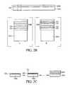
- FIG. 2Aillustrates a transmission line in accordance with a first exemplary embodiment of the invention.
- the embodimentincludes a pair of shield lines 202 - 1 , 202 - 2 depicted on opposing sides of a transmission line 201 .
- the inventionmay include any number of transmission lines 201 between any number of shield lines 202 - 1 , 202 - 2 .
- the transmission line 201 and the shield lines 202 - 1 , 202 - 2are spaced parallel to one another.
- the transmission line 201is spaced between a pair of sandwich layers 204 and 205 .
- the sandwich layers 204 , 205each include a conductive plane 204 A, 205 A and a shield layer 204 B, 205 B.
- the transmission line 201 and the shield lines 202 - 1 , 202 - 2are separated from one another and from the pair of sandwich layers 204 , 205 by an insulating material 206 , which may be an oxide or other low k dielectric.
- an electrical signal transmitted via the transmission line 201will induce a magnetic field surrounding the transmission line 201 .
- a magnetic fieldis illustrated by magnetic field lines 211 .
- the shield lines 202 - 1 , 202 - 2 and the shield layers 204 B, 205 Bprovide magnetic shielding to reduce the amount of magnetically induced noise on neighboring transmission lines (not shown).
- the magnetic fieldis confined in the x and y directions.
- the conductive planes 204 A, 205 A of the sandwich layers 204 and 205 respectively,provide electric field confinement.
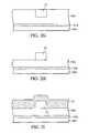
- the formation of the embodiment of FIG. 2Ais described in connection with FIGS. 2B-2K .
- FIG. 2Bshows the initial steps of fabrication of the FIG. 2A structure 200 .
- a first electrically conductive plane 204 Ais formed on a substrate (not shown) by depositing a layer of electrically conductive material using a technique such as evaporation, sputtering, or electroplating.
- the conductive planemay be formed of copper, aluminum, or any other suitable electrically conductive material.
- a shield layer 204 Bis formed on the first conductive plane 204 A. Together, conductive plane 204 A and shield layer 204 B are referred to as a sandwich layer 204 .
- the shield layer 204 Bis formed of shield material.
- shield materialis formed of films of a magnetic material 234 and an insulating material 224 .
- the films of magnetic material 234 and insulating material 224are alternated to form a desired layering pattern.
- the magnetic material 234may be a composite magnetic material 234 .
- the magnetic material 234is itself formed of layers of two or more materials that are alternated to form a desired layering pattern.
- the characteristics of multilayer films including non-magnetic materials, as well as magnetic materials, such as NiFe or Fe,have been shown to have higher effective permeabilities at higher frequencies than simple layers of magnetic materials by themselves. (See generally, M. Senda, “Permeability Measurement of Soft Magnetic Films at High Frequency and Multilayering Effect,” IEEE Translation of J. Magnetics in Japan, Vol. 8, No. 3, pp. 161-168, March 1993).
- the magnetic material 234is formed of alternating films of Ni and Fe, where the layering pattern is a repetitious Ni/Fe structure forming an NiFe film; and the insulating material 224 is SiO 2 .
- the NiFe filmis alternated with a film of SiO 2 in a repetitious NiFe/SiO 2 pattern to form a layer of shield material as shown in FIG. 2B , enlargement a.
- Each film of NiFeis approximately 50 nm thick, and each film of SiO 2 is approximately 100 nm thick.
- the film of magnetic material 234has a structure such that the Fe film does not contact the insulating material 224 .
- the magnetic material 234is Fe and the insulating material 224 is SiO 2 .
- Films of Fe and films of SiO 2are alternated to have a repetitious Fe/SiO 2 structure forming an Fe/SiO 2 film.
- the Fe/SiO 2 filmis further alternated with a film of SiO 2 to have a repetitious (Fe/SiO 2 )/SiO 2 structure forming a layer of shield material as shown in FIG. 2B , enlargement b.
- the film of Fe in the Fe/SiO 2 filmis approximately 7 nm thick
- the film of SiO 2 in the Fe/SiO 2 filmis approximately 2.5 nm thick
- the film of SiO 2 alternated with the Fe/SiO 2 filmis approximately 50 nm thick.
- NiFe thin filmsreadily oxidize when annealed at temperatures of 400° C. in conventional air, and oxidation begins to occur at temperatures as low as 300° C.
- a layering structurewhich also includes SiO 2 , Fe is still oxidized, even when annealing occurs at very low pressures. Oxidation of Fe results in the formation of a metal oxide layer, typically Fe 2 O 3 , which can be as thick as 20 nm. This causes the concentration of Fe in the NiFe layer to decrease and leads to degradation in the properties of the layer.
- PVDPhysical Vapor Deposition
- ALDatomic layer deposition
- ALDis a process for growing semiconductor films based on stepwise formation of individual atomic layers on a substrate. ALD permits uniform film thickness; lower sintering temperatures, if any; effective step coverage; very low pinhole density, or higher density of the deposited films; and potential elimination of gas phase reactions. See M. Herman, “Atomic Layer Epitaxy—12 Years Later,” Vacuum, Vol. 42, Nos. 1/2, pp. 61-66, 1991, which is incorporated herein by reference.
- the shield layer 204 Bis formed by ALD.
- monolayers of Ni and Feare alternatively deposited until the NiFe film reaches a desired thickness.
- FIG. 2Cillustrates formation of a layer of shield material on the conductive plane 204 A to Ni and Fe reactants.
- a monolayer 220 of Niis deposited over the conductive plane 204 A.
- a monolayer 221 of Feis deposited over the monolayer 220 of Ni.
- Monolayers 220 and 221 of Ni and Fe respectively,are alternatively deposited until the NiFe film has reached a desired thickness.
- a monolayer of Niis on top to reduce the oxidation of Fe.
- monolayers of SiO 2are similarly deposited to a desired thickness.
- the ALD processis then repeated until the shield layer 204 B has a desired thickness.
- FIG. 2Benlargement a, illustrates the layering structure of shield material where NiFe is the magnetic material 234 and SiO 2 is the insulating material 224 .
- a number of NiFe films 234are alternated with a number of SiO 2 films 224 to create a layer of shield material with a desired thickness, yielding an NiFe/SiO 2 structure.
- Enlargement b, FIG. 2Billustrates an embodiment where the shield material has an (Fe/SiO 2 )/SiO 2 structure.
- shield materialis formed of alternating films of magnetic material 234 and insulating material 224 by ALD as described in connection with FIGS. 2B and 2C .
- the shield material for this embodiment, and for the embodiments described belowpreferably has an NiFe/SiO 2 or an (Fe/SiO 2 )/SiO 2 structure as described in connection with FIGS. 2B and 2C . Therefore, the fabrication of structures formed of shield material will be described more generally henceforth.
- a first insulating layer 206 Ais formed over the shield layer 204 B.
- the insulating layer 206 Amay be an oxide or other low k dielectric and may be formed by conventional methods, such as chemical vapor deposition (CVD).
- FIG. 2Edepicts an opening 21 formed by conventional techniques in insulating layer 206 A where a transmission line 201 ( FIG. 2A ) is to be formed.
- FIG. 2Fdepicts a layer 25 of electrically conductive material deposited over the insulating layer 206 A filling opening 21 .
- the electrically conductive layer 25may be formed by conventional techniques such as evaporation, sputtering, or electroplating.
- the electrically conductive layer 25may be formed of copper, aluminum, or any other suitable electrically conductive material.
- FIG. 2Gdepicts removal of the excess conductive material leaving only the portion of the conductive material filling opening 21 ( FIG. 2E ) to form a transmission line 201 .
- the excess conductive materialmay be removed by conducting a chemical mechanical polish (CMP) step.
- FIG. 2Hdepicts performance of an etchback step to remove a portion of the first insulating layer 206 A from the sides of transmission line 201 , fully exposing both lateral sides of transmission line 201 .
- transmission line 201may be formed over the first insulating layer 206 A using optical lithography followed by an additive metallization, such as lift-off evaporation or electroplating to achieve the structure illustrated in FIG. 2 H.
- a layer of shield material 26is formed over first insulating layer 206 A and transmission line 201 . It is again noted that the layer of shield material 26 is formed by ALD as described above in connection with FIGS. 2B and 2C . As illustrated in FIG. 2J , the shield material is patterned and excess shield material is removed to form shield lines 202 - 1 , 202 - 2 on opposing sides of transmission line 201 .
- FIG. 2Kdepicts a second layer of insulating material is formed over the first layer of insulating material 206 A, the transmission line 201 , and the pair of shield lines 202 - 1 , 202 - 2 , to form a single insulating layer 206 .
- Insulating layer 206is over sandwich layer 204 and surrounds the transmission line 201 , and the pair of shield lines 202 - 1 , 202 - 2 .
- a second sandwich layer 205is formed over insulating layer 206 similar to the sandwich layer 204 described in connection with FIGS. 2B and 2C .
- a shield layer 205 Bis formed over insulating layer 206 , followed by the formation of a conductive plane 205 A to achieve the structure 200 depicted in FIG. 2 A.
- the shield layers 204 B and 205 B of sandwich layers 204 and 205 respectivelyare formed on the inside of the conductive planes 204 A and 205 A adjacent to the transmission line 201 .
- the shield layers 204 B and 205 Bmay also be formed on the outside of the conductive planes 204 A and 205 A. In such case, the conductive plane 204 A would be formed over shield layer 204 B and shield layer 205 B would be formed over conductive plane 205 A. Similar modifications may be made to the other embodiments described herein.
- the embodiment shown in FIG. 2Amay be formed without shield layers 204 B and 205 B.
- a first insulating layer 206 Awould be formed over conductive plane 204 A and conductive plane 205 A would be formed directly over insulating layer 206 .
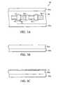
- FIG. 3Aillustrates neighboring transmission lines in accordance with a second exemplary embodiment of the invention.
- a number of transmission lines, 301 - 1 , 301 - 2are interspaced between a number of shield lines 302 - 1 , 302 - 2 .
- a pair of transmission lines 301 - 1 , 301 - 2are shown between a pair of shield lines 302 - 1 , 302 - 2 , but the invention has application to any number of transmission lines between any number of shield lines.
- the transmission lines 301 - 1 , 301 - 2 and the shield lines 302 - 1 , 302 - 2are spaced parallel to one another.
- the transmission lines 301 - 1 , 301 - 2are spaced between a pair of conductive planes 304 A and 305 A.
- the transmission lines 301 - 1 , 301 - 2 and the shield lines 302 - 1 , 302 - 2are separated from one another and from the pair of conductive planes 304 A and 305 A by an insulating layer 306 , which may be an oxide.
- the transmission lines 301 - 1 , 301 - 2include shield layers 315 formed on a number of surfaces thereon.
- the shield layers 315are formed on two surfaces of the transmission lines 301 - 1 , 301 - 2 including opposing sides adjacent to the conductive planes 304 A, 305 A.
- An electrical signal transmitted via the transmission lines 301 - 1 , 301 - 2will induce a magnetic field surrounding the transmission lines 301 - 1 , 301 - 2 .
- Such a magnetic fieldis illustrated by magnetic field lines 311 .
- the shield layers 315formed on a number of surfaces of the transmission lines 301 - 1 , 301 - 2 , and the shield lines 302 - 1 , 302 - 2 provide magnetic shielding to reduce the amount of magnetically induced noise on neighboring transmission lines, e.g. 301 - 1 and 301 - 2 .
- the magnetic field lines 311illustrate this magnetic shielding effect. This embodiment provides for magnetic confinement in all directions.
- FIG. 3A structure 300Formation of the FIG. 3A structure 300 is illustrated by FIGS. 3B-3J .
- a first conductive plane 304 Ais formed on a substrate (not shown) by depositing a layer of electrically conductive material using a technique such as evaporation, sputtering, or electroplating.
- the layer of electrically conductive materialmay be a layer of copper, aluminum, or any other suitable electrically conductive material.
- a first insulating layer 306 Ais formed on the conductive plane 304 A, by conventional methods, such as CVD.
- FIG. 3Cdepicts a first layer of shield material 36 formed over the insulating layer 306 A by ALD.
- the first layer of shield material 36is formed as described above in connection with FIGS. 2B-C .
- FIG. 3Ddepicts a layer of electrically conductive material 33 formed over the first layer of shield material 36 .
- the layer of electrically conductive material 33may be formed using a technique such as evaporation, sputtering, or electroplating a layer of copper, aluminum, or any other suitable electrically conductive material.
- FIG. 3Edepicts the removal of the excess shield material and electrically conductive material by conventional techniques, leaving partially formed transmission lines 301 - 1 , 301 - 2 having a layer of electrically conductive material 33 over a first layer of shield material 36 .
- the first layer of shield material 36forms shield layers 315 ( FIG. 3A ) on a bottom surface of the transmission lines 301 - 1 , 302 - 1 .
- FIG. 3Fa second layer of insulating material 306 B is then formed over the first layer of insulating material 306 A ( FIG. 3E ) and over the partially formed transmission lines 301 - 1 , 301 - 2 to form a single insulating layer 306 B.
- FIG. 3Fdepicts results of a first CMP step to expose the conductive layer 33 of the partially formed transmission lines 301 - 1 , 301 - 2 .
- FIG. 3Gdepicts the insulating layer 306 B patterned to form openings 35 for the formation of shield lines 302 - 1 , 302 - 2 .
- openings 35are formed between and parallel to the partially formed transmission lines 301 - 1 , 301 - 2 .
- FIG. 3Hdepicts the results of an etchback step to partially remove a portion of conductive layer 33 forming openings 36 , which are sufficient to form shield layers 315 on a top surface of the transmission lines 301 - 1 , 301 - 2 .
- a second layer of shield material 37is then formed by ALD over the insulating layer 306 B and over the partially formed transmission lines 301 - 1 and 301 - 2 filling openings 35 and 36 .
- the second layer of shield material 37is formed in the manner described above in connection with FIGS. 2B-2C .
- a second CMP stepis performed ( FIG. 3J ) to remove excess shield material and expose the surface of insulating layer 306 B.
- the shield material filling openings 35forms the shield lines 302 - 1 , 302 - 2 .
- the shield material filling openings 36forms the shield layers 315 on a top surface of transmission lines 301 - 1 , 301 - 2 .
- a third layer of insulating materialis formed over the second insulating layer 306 B, the transmission lines 301 - 1 , 301 - 2 , and the shield lines 302 - 1 , 302 - 2 to create a single insulating layer 306 .
- a second conductive plane 305 Ais formed over the insulating layer 306 to achieve the structure 300 shown in FIG. 3 A.
- forming the pair of conductive planes 304 A and 305 Ais optional, and conductive planes 304 A and 305 A may be omitted.
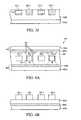
- FIG. 4Aillustrates neighboring transmission lines in accordance with a third exemplary embodiment of the invention.
- a number of transmission lines 401 - 1 , 401 - 2are spaced between a number of electrically conductive lines 402 - 1 , 402 - 2 , which are grounded.
- a pair of transmission lines 401 - 1 , 401 - 2 and a pair of electrically conductive lines 402 - 1 , 402 - 2are shown, but the invention has applicability to any number of transmission lines spaced between any number of electrically conductive lines.
- the transmission lines 401 - 1 , 401 - 2 and the electrically conductive lines 402 - 1 , 402 - 2are spaced parallel to one another.
- the transmission lines 401 - 1 , 401 - 2are spaced between a pair of sandwich layers 404 and 405 .
- the electrically conductive lines 401 - 1 , 401 - 2include shield layers 415 formed on a number of surfaces thereon.
- the shield layers 415are formed on two surfaces of the conductive lines 401 - 1 , 401 - 2 , including opposing sides adjacent to the transmission lines 401 - 1 , 401 - 2 .
- An electrical signal transmitted via the transmission lines 401 - 1 , 401 - 2will induce a magnetic field surrounding the transmission lines 401 - 1 , 401 - 2 .
- Such a magnetic fieldis illustrated by magnetic field lines 411 .
- the shield layers 415 on the electrically conductive lines 402 - 1 , 402 - 2 and the shield layers 404 B, 405 B of the sandwich layers 404 , 405 respectivelyprovide magnetic shielding to reduce the amount of magnetically induced noise on neighboring transmission lines, e.g. 401 - 1 and 401 - 2 .
- the magnetic field lines 411illustrate this magnetic shielding effect.
- the conductive planes 404 A, 405 A of the sandwich layers 404 , 405 respectively, and the electrically conductive lines 402 - 1 , 402 - 2provide electric field confinement. In the embodiment of FIG. 4A , both the electric and magnetic fields are confined in the x and y directions.
- the formation of the FIG. 4A structure 400will be described in connection with FIGS. 4B-4E .
- a first insulating layer 406 Ais formed over a sandwich layer 404 , as described in connection with FIGS. 2B-2D above.
- transmission lines 401 - 1 , 401 - 2 and electrically conductive lines 402 - 1 , 402 - 2are formed of an electrically conductive material over the insulating layer 406 A by conventional methods, such as optical lithography followed by an additive metallization, such as lift-off evaporation or electroplating.
- the transmission lines 401 - 1 , 401 - 2 and the electrically conductive lines 402 - 1 , 402 - 2may be formed of copper, aluminum, or any other suitable electrically conductive material.
- the transmission lines 401 - 1 , 401 - 2may transmit a signal, whereas the electrically conductive lines 402 - 1 , 402 - 2 are grounded ( FIG. 4A ) and do not transmit a signal.
- a layer of shield material 46is formed over the transmission lines 401 - 1 , 401 - 2 , the electrically conductive lines 402 - 1 , 402 - 2 , and the insulating layer 406 A.
- a facet etch stepis conducted to remove the shield material from the surfaces of the transmission lines 401 - 1 , 401 - 2 , the electrically conductive lines 402 - 1 , 402 - 2 , and the insulating layer 406 A.
- Shield materialremains on lateral sides of the transmission lines 401 - 1 , 401 - 2 and electrically conductive lines 402 - 1 , 402 - 2 , as shown in FIG. 4 D.
- FIG. 4Edepicts the removal of excess shield material on transmission lines 401 - 1 and 401 - 2 by known techniques.
- the structure 400is completed as described above in connection with FIG. 2K.
- a second insulating layer 406is formed over the transmission lines 401 - 1 , 401 - 2 , the electrically conductive lines 402 - 1 , 402 - 2 , and the first insulating layer 406 A, to form a single insulating layer 406 ; and a sandwich layer 405 is formed over the insulating layer 406 .
- the structure 400 of FIG. 4Ais achieved.
- FIG. 5Aillustrates neighboring transmission lines in accordance with a fourth exemplary embodiment of the invention.
- a number of transmission lines 501 - 1 , 501 - 2are spaced between a number of electrically conductive lines 502 - 1 , 502 - 2 , which are grounded.
- a pair of transmission lines 501 - 1 , 501 - 2 and a pair of electrically conductive lines 502 - 1 , 502 - 2are shown, but the invention has applicability to any number of transmission lines spaced between any number of electrically conductive lines.
- the transmission lines 501 - 1 , 501 - 2 and the electrically conductive lines 502 - 1 , 502 - 2are spaced parallel to one another.
- the transmission lines 501 - 1 , 501 - 2are spaced between a conductive plane 504 A and a sandwich layer 505 .
- the transmission lines 501 - 1 , 501 - 2 and the electrically conductive lines 502 - 1 , 502 - 2include shield layers 515 formed on a number of surfaces thereon.
- shield layers 515are formed on three surfaces of the transmission lines 501 - 1 , 501 - 2 and the electrically conductive lines 502 - 1 , 502 - 2 .
- the three surfacesinclude opposing sides adjacent to the neighboring electrically conductive lines 502 - 1 , 502 - 2 or transmission lines 501 - 1 , 501 - 2 respectively, and on a side adjacent to the conductive plane 504 A.
- An electrical signal transmitted via the transmission lines 501 - 1 , 501 - 2will induce a magnetic field surrounding the transmission lines 501 - 1 , 501 - 2 .
- a magnetic fieldis illustrated by magnetic field lines 511 .
- the shield layers 515 formed on a number of surfaces of the transmission lines 501 - 1 , 501 - 2 and the electrically conductive lines 502 - 1 , 502 - 2 , and the shield layer 505 B of sandwich layer 505provide magnetic shielding to reduce the amount of magnetically induced noise on neighboring transmission lines, e.g. 501 - 1 and 501 - 2 .
- the magnetic field lines 511illustrate this magnetic shielding effect.
- conductive planes 504 A, 505 A and the electrically conductive lines 502 - 1 , 502 - 2provide electric field confinement.
- FIG. 5A structure 500will be described in connection with FIGS. 5B-5E .
- a first insulating layer 506 A having openings 51 for the formation of transmission lines and electrically conductive linesis formed over a conductive plane 504 A.
- the formation of the structure illustrated in FIG. 5Bis conducted similarly to that described in connection with FIGS. 2B-2E , except that the formation of a shield layer over the conductive plane 504 A is omitted.
- a layer of shield material 56is formed by ALD over the first insulating layer 506 A and on the sides and bottoms of openings 51 to a desired thickness, but not filling openings 51 .
- the layer of shield material 56 on the sides and bottoms of openings 51will form the shield layers 515 on the three surfaces of the transmission lines 501 - 1 , 501 - 2 and the electrically conductive lines 502 - 1 , 502 - 2 .
- FIG. 5Ddepicts a layer of electrically conductive material 55 formed over the shield layer 56 filling the openings 51 .
- the layer of electrically conductive material 55may be formed by evaporation, sputtering, or electroplating, and may be a layer of copper, aluminum, or any other suitable electrically conductive material.
- FIG. 5Edepicts the results of a CMP step to remove excess conductive material and excess shield material, leaving transmission lines 501 - 1 , 502 - 1 and electrically conductive lines 502 - 1 , 502 - 2 , both having shield layers 515 formed on three sides thereof.
- the structure 500 of the embodiment shown in FIG. 5Amay then be completed as described in connection with FIG. 3J , except that a sandwich layer 505 is formed over the insulating layer 506 . Otherwise stated, a shield layer 505 B is formed between the insulating layer 506 and the conductive plane 505 A. Thereby, the structure 500 shown in FIG. 5A is achieved.
- FIG. 5Aillustrates an embodiment that is easy to manufacture.
- FIG. 6Ashows a very similar alternate configuration to that shown in FIG. 5 A.
- the number of transmission lines 601 - 1 , 601 - 2do not have shield layers formed thereon.
- FIG. 7depicts another very similar alternate configuration.
- the electrically conductive lines 602 - 1 , 602 - 2do not have shield layers formed thereon.
- FIG. 6Aillustrates neighboring transmission lines in accordance with a fifth embodiment of the invention.
- a number of transmission lines 601 - 1 , 601 - 2are spaced between a number of electrically conductive lines 602 - 1 , 602 - 2 , which are shown grounded.
- a pair of transmission lines 601 - 1 , 601 - 2 and a pair of electrically conductive lines 602 - 1 , 602 - 2are shown, but the invention has applicability to any number of transmission lines spaced between any number of electrically conductive lines.
- the transmission lines 601 - 1 , 601 - 2 and the electrically conductive lines 602 - 1 , 602 - 2are spaced parallel to one another.
- the transmission lines 601 - 1 , 601 - 2are spaced between a conductive plane 604 A and a sandwich layer 605 . Further, in this embodiment, the transmission lines 601 - 1 , 601 - 2 include shield layers 615 formed on a number of surfaces thereon. Preferably, shield layers 615 are formed on three surfaces of the transmission lines 601 - 1 , 601 - 2 , including opposing sides adjacent to the electrically conductive lines 602 - 1 , 602 - 2 , and on a side adjacent to the conductive plane 604 A.
- An electrical signal transmitted via the transmission lines 601 - 1 , 601 - 2will induce a magnetic field surrounding the transmission lines 601 - 1 , 601 - 2 .
- a magnetic fieldis illustrated by magnetic field lines 611 .
- the shield layers 615 on the transmission lines 601 - 1 , 601 - 2 and the shield layer 605 B of sandwich layer 605provide magnetic shielding to reduce the amount of magnetically induced noise on neighboring transmission lines, e.g. 601 - 1 and 601 - 2 .
- the magnetic field lines 611illustrate this magnetic shielding effect.
- FIG. 6A structure 600is described in connection with FIGS. 6B-6E .
- FIG. 6Bthere is a conductive plane 604 A below a first layer of insulating material 606 A.
- the transmission lines 601 - 1 , 601 - 2are formed having shield layers 615 on lateral sides thereof and on a side thereof adjacent to the conductive plane 604 A.
- the structure illustrated in FIG. 6Bis formed similarly to that of the structure illustrated in FIG. 5E , except that only transmission lines 601 - 1 , 601 - 2 are formed.
- openings 61are formed in the insulating layer 606 A where electrically conductive lines 602 - 1 , 602 - 2 are to be formed.
- FIG. 6Ddepicts a layer of electrically conductive material deposited over the transmission lines 601 - 1 , 601 - 2 and the insulating layer 606 A, filling the openings 61 to form electrically conductive lines 602 - 1 , 602 - 2 .
- the layer of electrically conductive material 65may be formed by evaporation, sputtering, or electroplating, and may be a layer of copper, aluminum, or any other suitable electrically conductive material.
- a CMP stepis performed removing the excess conductive material and exposing the surfaces of the insulating layer 606 A, the transmission lines 601 - 1 , 601 - 2 , and the electrically conductive lines 602 - 1 , 602 - 2 , as shown in FIG. 6 E.
- the structure 600may be completed as described in connection with FIG. 3J , except that a sandwich layer 605 is formed over the insulating layer 606 . Otherwise stated, a shield layer 605 B is formed between the insulating layer 606 and the conductive plane 605 A. Thereby, the structure 600 depicted in FIG. 6A is achieved.
- FIG. 7illustrates neighboring transmission lines in accordance with a sixth embodiment of the invention.
- a number of transmission lines 701 - 1 , 701 - 2are spaced between a number of electrically conductive lines 702 - 1 , 702 - 2 , which are grounded.
- a pair of transmission lines 701 - 1 , 701 - 2 and a pair of electrically conductive lines 702 - 1 , 702 - 2are shown, but the invention has applicability to any number of transmission lines spaced between any number of electrically conductive lines.
- the transmission lines 701 - 1 , 701 - 2 and the electrically conductive lines 702 - 1 , 702 - 2are spaced parallel to one another.
- the transmission lines 701 - 1 , 701 - 2are spaced between sandwich layers 704 and 705 .
- the electrically conductive lines 702 - 1 , 702 - 2include shield layers 715 formed on a number of surfaces thereof.
- shield layers 715are formed on three surfaces of the electrically conductive lines 702 - 1 , 702 - 2 , including opposing sides adjacent to the transmission lines 701 - 1 , 702 , and on a side adjacent to the sandwich layer 704 .
- an electrical signal transmitted via the transmission lines 701 - 1 , 701 - 2will induce a magnetic field surrounding the transmission lines 701 - 1 , 701 - 2 .
- Such a magnetic fieldis illustrated by magnetic field lines 711 .
- the magnetic field lines 711illustrate this magnetic shielding effect.
- the conductive planes 704 A, 705 A and the number of electrically conductive lines 702 - 1 , 702 - 2provide electric field confinement.
- FIG. 7 having a structure 700is easy to manufacture, and is formed as described in connection with FIGS. 6B-6E with minor differences: a sandwich layer 704 is formed over the substrate (not shown), and the shield layers 715 are formed on the electrically conductive lines 702 - 1 , 702 - 1 , instead of on the transmission lines 701 - 1 , 701 - 2 .
- FIG. 7is a configuration similar to that of FIG. 6A , but allows for more space to be used for the transmission lines 701 - 1 , 701 - 2 , since they are not covered by shield material.
- the conductive planes described in connection with the different embodimentsmay be independently coupled to a ground or power supply bus. Further, the insulating layer described in connection with the different embodiments may be an oxide layer or other low k dielectric.
- FIG. 8is a block diagram of a system employing a transmission line circuit in accordance with a seventh exemplary embodiment of the invention.
- the system 800uses current signaling.
- the system 800includes a low output impedance driver 810 .
- the low output impedance driver 810is coupled to a transmission line circuit 820 .
- the transmission line circuit 820is a transmission line circuit such as any one of the transmission line circuits described above in connection with FIGS. 2A-7 .
- the system 800includes a termination circuit 830 having a termination impedance that is matched to the impedance of the transmission line circuit 820 .
- FIG. 9is a block diagram of a system employing an interconnection structure in accordance with an eighth exemplary embodiment of the invention.
- the system 900includes an integrated circuit 910 .
- the integrated circuit 910includes a transmission line circuit such as any one of the transmission line circuits described and presented above with reference to FIGS. 2A-7 .
- the structure 200 of FIG. 2Ais included in the integrated circuit 910 .
- the system 900includes a processor 920 that is operatively coupled to the integrated circuit 910 .
- the processor 920is coupled to the integrated circuit 910 through a system bus 930 .
- FIG. 10is a block diagram of a system employing an interconnection structure in accordance with a ninth exemplary embodiment of the invention
- FIG. 10depicts a processor-based system 1000 utilizing a transmission line circuit such as any one of the transmission line circuits described above in connection with FIGS. 2A-7 .
- bus 1060 coupling the CPU 1002 with the bus 1020contains a transmission line structure 200 , as depicted in FIG. 2 A.
- the processor-based system 1000may be a computer system, a process control system or any other system employing a processor and associated memory.
- the system 1000includes a central processing unit (CPU) 1002 , e.g., a microprocessor, that communicates with the RAM 1012 and an I/O device 1008 over a bus 1020 .
- CPUcentral processing unit
- the bus 1020may be a series of buses and bridges commonly used in a processor-based system, but for convenience purposes only, the bus 1020 has been illustrated as a single bus.
- the processor-based system 1000also includes read-only memory (ROM) 1014 and may include peripheral devices such as a floppy disk drive 1004 and a compact disk (CD) ROM drive 1006 that also communicates with the CPU 1002 over the bus 1020 as is well known in the art.
- ROMread-only memory
- CDcompact disk
- inductive couplingcan be minimized by: (i) magnetic shields above and below transmission lines, and/or (ii) magnetic shields between transmission lines.
- These magnetic shieldsmay be: (i) manufactured using ALD techniques, where thin layers of the magnetic material are alternated by thin layers of insulators, on the order of 5 nanometers (nm), which can only be formed effectively by employing ALD techniques; (ii) formed so that the magnetic material deposited does not require high sintering or annealing temperatures; (iii) formed so that the layering structure prevents oxidation of the magnetic material; and (iv) able to provide good surface coverage with improved density and therefore superior magnetic properties.
Landscapes
- Physics & Mathematics (AREA)
- Engineering & Computer Science (AREA)
- Microelectronics & Electronic Packaging (AREA)
- Condensed Matter Physics & Semiconductors (AREA)
- General Physics & Mathematics (AREA)
- Computer Hardware Design (AREA)
- Power Engineering (AREA)
- Electromagnetism (AREA)
- Health & Medical Sciences (AREA)
- Toxicology (AREA)
- Semiconductor Integrated Circuits (AREA)
Abstract
Description
Claims (93)
Priority Applications (2)
| Application Number | Priority Date | Filing Date | Title |
|---|---|---|---|
| US10/443,021US6970053B2 (en) | 2003-05-22 | 2003-05-22 | Atomic layer deposition (ALD) high permeability layered magnetic films to reduce noise in high speed interconnection |
| US11/063,132US7154354B2 (en) | 2003-05-22 | 2005-02-22 | High permeability layered magnetic films to reduce noise in high speed interconnection |
Applications Claiming Priority (1)
| Application Number | Priority Date | Filing Date | Title |
|---|---|---|---|
| US10/443,021US6970053B2 (en) | 2003-05-22 | 2003-05-22 | Atomic layer deposition (ALD) high permeability layered magnetic films to reduce noise in high speed interconnection |
Related Child Applications (1)
| Application Number | Title | Priority Date | Filing Date |
|---|---|---|---|
| US11/063,132ContinuationUS7154354B2 (en) | 2003-05-22 | 2005-02-22 | High permeability layered magnetic films to reduce noise in high speed interconnection |
Publications (2)
| Publication Number | Publication Date |
|---|---|
| US20040233010A1 US20040233010A1 (en) | 2004-11-25 |
| US6970053B2true US6970053B2 (en) | 2005-11-29 |
Family
ID=33450329
Family Applications (2)
| Application Number | Title | Priority Date | Filing Date |
|---|---|---|---|
| US10/443,021Expired - LifetimeUS6970053B2 (en) | 2003-05-22 | 2003-05-22 | Atomic layer deposition (ALD) high permeability layered magnetic films to reduce noise in high speed interconnection |
| US11/063,132Expired - LifetimeUS7154354B2 (en) | 2003-05-22 | 2005-02-22 | High permeability layered magnetic films to reduce noise in high speed interconnection |
Family Applications After (1)
| Application Number | Title | Priority Date | Filing Date |
|---|---|---|---|
| US11/063,132Expired - LifetimeUS7154354B2 (en) | 2003-05-22 | 2005-02-22 | High permeability layered magnetic films to reduce noise in high speed interconnection |
Country Status (1)
| Country | Link |
|---|---|
| US (2) | US6970053B2 (en) |
Cited By (23)
| Publication number | Priority date | Publication date | Assignee | Title |
|---|---|---|---|---|
| US20030174529A1 (en)* | 2002-03-13 | 2003-09-18 | Micron Technology, Inc. | High permeability layered films to reduce noise in high speed interconnects |
| US20050006727A1 (en)* | 2002-03-13 | 2005-01-13 | Micron Technology, Inc. | High permeability composite films to reduce noise in high speed interconnects |
| US20050030780A1 (en)* | 2002-02-06 | 2005-02-10 | Infineon Technologies Ag | Memory cell |
| US20070047310A1 (en)* | 2005-08-30 | 2007-03-01 | Micron Technology, Inc. | NAND memory device and programming methods |
| US20080121976A1 (en)* | 2006-08-03 | 2008-05-29 | Micron Technology, Inc. | Non-volatile memory cell devices and methods |
| US20080121969A1 (en)* | 2006-08-03 | 2008-05-29 | Micron Technology, Inc. | Non-volatile memory cell device and methods |
| US7410917B2 (en) | 2002-12-04 | 2008-08-12 | Micron Technology, Inc. | Atomic layer deposited Zr-Sn-Ti-O films using TiI4 |
| US7410910B2 (en) | 2005-08-31 | 2008-08-12 | Micron Technology, Inc. | Lanthanum aluminum oxynitride dielectric films |
| US7446368B2 (en) | 2001-08-30 | 2008-11-04 | Micron Technology, Inc. | Deposition of metal oxide and/or low asymmetrical tunnel barrier interpoly insulators |
| US20090109734A1 (en)* | 2007-10-26 | 2009-04-30 | Micron Technology, Inc. | Non-volatile sram cell |
| US7554829B2 (en) | 1999-07-30 | 2009-06-30 | Micron Technology, Inc. | Transmission lines for CMOS integrated circuits |
| US7560793B2 (en) | 2002-05-02 | 2009-07-14 | Micron Technology, Inc. | Atomic layer deposition and conversion |
| US7560395B2 (en) | 2005-01-05 | 2009-07-14 | Micron Technology, Inc. | Atomic layer deposited hafnium tantalum oxide dielectrics |
| US7572695B2 (en) | 2005-05-27 | 2009-08-11 | Micron Technology, Inc. | Hafnium titanium oxide films |
| US7588988B2 (en) | 2004-08-31 | 2009-09-15 | Micron Technology, Inc. | Method of forming apparatus having oxide films formed using atomic layer deposition |
| US7611959B2 (en) | 2002-12-04 | 2009-11-03 | Micron Technology, Inc. | Zr-Sn-Ti-O films |
| US7662729B2 (en) | 2005-04-28 | 2010-02-16 | Micron Technology, Inc. | Atomic layer deposition of a ruthenium layer to a lanthanide oxide dielectric layer |
| US7670646B2 (en) | 2002-05-02 | 2010-03-02 | Micron Technology, Inc. | Methods for atomic-layer deposition |
| US7692222B2 (en) | 2006-11-07 | 2010-04-06 | Raytheon Company | Atomic layer deposition in the formation of gate structures for III-V semiconductor |
| US7719065B2 (en) | 2004-08-26 | 2010-05-18 | Micron Technology, Inc. | Ruthenium layer for a dielectric layer containing a lanthanide oxide |
| US8501563B2 (en) | 2005-07-20 | 2013-08-06 | Micron Technology, Inc. | Devices with nanocrystals and methods of formation |
| US20160029477A1 (en)* | 2013-02-27 | 2016-01-28 | Nec Corporation | Wiring substrate, semiconductor device, printed board, and method for producing wiring substrate |
| US9627501B2 (en) | 2005-08-30 | 2017-04-18 | Micron Technology, Inc. | Graded dielectric structures |
Families Citing this family (26)
| Publication number | Priority date | Publication date | Assignee | Title |
|---|---|---|---|---|
| US6852167B2 (en) | 2001-03-01 | 2005-02-08 | Micron Technology, Inc. | Methods, systems, and apparatus for uniform chemical-vapor depositions |
| US8026161B2 (en) | 2001-08-30 | 2011-09-27 | Micron Technology, Inc. | Highly reliable amorphous high-K gate oxide ZrO2 |
| US7068544B2 (en) | 2001-08-30 | 2006-06-27 | Micron Technology, Inc. | Flash memory with low tunnel barrier interpoly insulators |
| US6900122B2 (en) | 2001-12-20 | 2005-05-31 | Micron Technology, Inc. | Low-temperature grown high-quality ultra-thin praseodymium gate dielectrics |
| US7101770B2 (en)* | 2002-01-30 | 2006-09-05 | Micron Technology, Inc. | Capacitive techniques to reduce noise in high speed interconnections |
| US7135421B2 (en) | 2002-06-05 | 2006-11-14 | Micron Technology, Inc. | Atomic layer-deposited hafnium aluminum oxide |
| US7221017B2 (en) | 2002-07-08 | 2007-05-22 | Micron Technology, Inc. | Memory utilizing oxide-conductor nanolaminates |
| US7221586B2 (en) | 2002-07-08 | 2007-05-22 | Micron Technology, Inc. | Memory utilizing oxide nanolaminates |
| US6921702B2 (en) | 2002-07-30 | 2005-07-26 | Micron Technology Inc. | Atomic layer deposited nanolaminates of HfO2/ZrO2 films as gate dielectrics |
| US7199023B2 (en) | 2002-08-28 | 2007-04-03 | Micron Technology, Inc. | Atomic layer deposited HfSiON dielectric films wherein each precursor is independendently pulsed |
| US7192892B2 (en) | 2003-03-04 | 2007-03-20 | Micron Technology, Inc. | Atomic layer deposited dielectric layers |
| US7183186B2 (en) | 2003-04-22 | 2007-02-27 | Micro Technology, Inc. | Atomic layer deposited ZrTiO4 films |
| US7601649B2 (en) | 2004-08-02 | 2009-10-13 | Micron Technology, Inc. | Zirconium-doped tantalum oxide films |
| US7494939B2 (en) | 2004-08-31 | 2009-02-24 | Micron Technology, Inc. | Methods for forming a lanthanum-metal oxide dielectric layer |
| US7374964B2 (en) | 2005-02-10 | 2008-05-20 | Micron Technology, Inc. | Atomic layer deposition of CeO2/Al2O3 films as gate dielectrics |
| US7683445B2 (en)* | 2005-02-24 | 2010-03-23 | Everspin Technologies, Inc. | Enhanced permeability device structures and method |
| US7545662B2 (en)* | 2005-03-25 | 2009-06-09 | Taiwan Semiconductor Manufacturing Co., Ltd. | Method and system for magnetic shielding in semiconductor integrated circuit |
| US7544596B2 (en) | 2005-08-30 | 2009-06-09 | Micron Technology, Inc. | Atomic layer deposition of GdScO3 films as gate dielectrics |
| US8071476B2 (en) | 2005-08-31 | 2011-12-06 | Micron Technology, Inc. | Cobalt titanium oxide dielectric films |
| US7709402B2 (en) | 2006-02-16 | 2010-05-04 | Micron Technology, Inc. | Conductive layers for hafnium silicon oxynitride films |
| US7563730B2 (en) | 2006-08-31 | 2009-07-21 | Micron Technology, Inc. | Hafnium lanthanide oxynitride films |
| US7759237B2 (en)* | 2007-06-28 | 2010-07-20 | Micron Technology, Inc. | Method of forming lutetium and lanthanum dielectric structures |
| KR101120508B1 (en)* | 2007-08-22 | 2012-02-29 | (주) 와이팜 | A layout structure for reducing an interference phenomenon |
| US9912448B2 (en)* | 2012-02-13 | 2018-03-06 | Sentinel Connector Systems, Inc. | Testing apparatus for a high speed communications jack and methods of operating the same |
| US10103494B2 (en)* | 2014-05-08 | 2018-10-16 | Apple Inc. | Connector system impedance matching |
| US20250006647A1 (en)* | 2023-06-29 | 2025-01-02 | International Business Machines Corporation | Crosstalk noise reduction by high permeability insulator |
Citations (71)
| Publication number | Priority date | Publication date | Assignee | Title |
|---|---|---|---|---|
| US3478230A (en) | 1967-04-17 | 1969-11-11 | United Aircraft Corp | Thermomagnetic generation of power in a superconductor |
| US3676718A (en) | 1971-03-26 | 1972-07-11 | Bell Telephone Labor Inc | Supercurrent structures utilizing mobil flux vortices |
| US3816673A (en) | 1971-01-25 | 1974-06-11 | Kokusai Denshin Denwa Co Ltd | Coaxial cable including at least one repeater |
| US4308421A (en) | 1978-01-18 | 1981-12-29 | Virginia Plastics Company | EMF Controlled multi-conductor cable |
| US4372032A (en) | 1979-09-04 | 1983-02-08 | The United States Of America As Represented By The Secretary Of The Navy | Normally off InP field effect transistor making process |
| US4640871A (en) | 1984-09-12 | 1987-02-03 | Sony Corporation | Magnetic material having high permeability in the high frequency range |
| US4749888A (en) | 1984-01-25 | 1988-06-07 | Agency Of Industrial Science & Technology | Josephson transmission line device |
| US4933743A (en) | 1989-03-11 | 1990-06-12 | Fairchild Semiconductor Corporation | High performance interconnect system for an integrated circuit |
| US4962476A (en) | 1988-07-26 | 1990-10-09 | Nec Corporation | Semiconductor memory device having bit lines less liable to have influences of the adjacent bit lines |
| US5019728A (en) | 1990-09-10 | 1991-05-28 | Ncr Corporation | High speed CMOS backpanel transceiver |
| US5128962A (en) | 1989-06-16 | 1992-07-07 | Texas Instruments Incorporated | Line interface circuit and a method of testing such a circuit |
| US5135889A (en) | 1991-12-09 | 1992-08-04 | Micron Technology, Inc. | Method for forming a shielding structure for decoupling signal traces in a semiconductor |
| US5165046A (en) | 1989-11-06 | 1992-11-17 | Micron Technology, Inc. | High speed CMOS driver circuit |
| US5223808A (en) | 1992-02-25 | 1993-06-29 | Hughes Aircraft Company | Planar ferrite phase shifter |
| US5352998A (en) | 1992-10-09 | 1994-10-04 | Mitsubishi Denki Kabushiki Kaisha | Microwave integrated circuit having a passive circuit substrate mounted on a semiconductor circuit substrate |
| US5363550A (en) | 1992-12-23 | 1994-11-15 | International Business Machines Corporation | Method of Fabricating a micro-coaxial wiring structure |
| US5450026A (en) | 1994-07-27 | 1995-09-12 | At&T Corp. | Current mode driver for differential bus |
| US5510758A (en) | 1993-04-07 | 1996-04-23 | Matsushita Electric Industrial Co., Ltd. | Multilayer microstrip wiring board with a semiconductor device mounted thereon via bumps |
| US5521536A (en) | 1993-08-06 | 1996-05-28 | Hitachi, Ltd. | Integrated circuit device having different signal transfer circuits for wirings with different lengths |
| US5619159A (en) | 1991-01-10 | 1997-04-08 | Fujitsu Limited | Signal processing device and a method for transmitting signal |
| US5656548A (en) | 1993-09-30 | 1997-08-12 | Kopin Corporation | Method for forming three dimensional processor using transferred thin film circuits |
| US5729047A (en) | 1996-03-25 | 1998-03-17 | Micron Technology, Inc. | Method and structure for providing signal isolation and decoupling in an integrated circuit device |
| US5772153A (en) | 1995-10-17 | 1998-06-30 | Abaunza; John T. | Aircraft icing sensors |
| US5811984A (en) | 1995-10-05 | 1998-09-22 | The Regents Of The University Of California | Current mode I/O for digital circuits |
| US5880601A (en) | 1994-06-13 | 1999-03-09 | Hitachi, Ltd. | Signal receiving circuit and digital signal processing system |
| US5910684A (en) | 1995-11-03 | 1999-06-08 | Micron Technology, Inc. | Integrated circuitry |
| US6075383A (en) | 1995-04-28 | 2000-06-13 | Siemens Aktiengesellschaft | GTL output amplifier for coupling an input signal present at the input into a transmission line present at the output |
| US6133621A (en) | 1998-10-15 | 2000-10-17 | Stmicroelectronics S.R.L. | Integrated shielded electric connection |
| US6143616A (en) | 1997-08-22 | 2000-11-07 | Micron Technology, Inc. | Methods of forming coaxial integrated circuitry interconnect lines |
| US20010000428A1 (en) | 1999-02-23 | 2001-04-26 | Abadeer Wagdi W. | Termination resistance independent system for impedance matching in high speed input-output chip interfacing |
| US6226599B1 (en) | 1997-03-05 | 2001-05-01 | Fujitsu Limted | Electromagnetic wave analyzer apparatus |
| US6255852B1 (en) | 1999-02-09 | 2001-07-03 | Micron Technology, Inc. | Current mode signal interconnects and CMOS amplifier |
| US6281042B1 (en) | 1998-08-31 | 2001-08-28 | Micron Technology, Inc. | Structure and method for a high performance electronic packaging assembly |
| US6350649B1 (en)* | 2000-10-30 | 2002-02-26 | Samsung Electronics Co., Ltd. | Bit line landing pad and borderless contact on bit line stud with etch stop layer and manufacturing method thereof |
| US6355561B1 (en) | 2000-11-21 | 2002-03-12 | Micron Technology, Inc. | ALD method to improve surface coverage |
| US6373740B1 (en) | 1999-07-30 | 2002-04-16 | Micron Technology, Inc. | Transmission lines for CMOS integrated circuits |
| US6420778B1 (en) | 2001-06-01 | 2002-07-16 | Aralight, Inc. | Differential electrical transmission line structures employing crosstalk compensation and related methods |
| US6433408B1 (en) | 1999-01-08 | 2002-08-13 | Nec Corporation | Highly integrated circuit including transmission lines which have excellent characteristics |
| US6461436B1 (en) | 2001-10-15 | 2002-10-08 | Micron Technology, Inc. | Apparatus and process of improving atomic layer deposition chamber performance |
| US20030045082A1 (en) | 2001-08-30 | 2003-03-06 | Micron Technology, Inc. | Atomic layer deposition of metal oxide and/or low asymmetrical tunnel barrier interploy insulators |
| US6541353B1 (en) | 2000-08-31 | 2003-04-01 | Micron Technology, Inc. | Atomic layer doping apparatus and method |
| US6545338B1 (en) | 1999-10-28 | 2003-04-08 | Koninklijke Philips Electronics N.V. | Methods for implementing co-axial interconnect lines in a CMOS process for high speed RF and microwave applications |
| US6551893B1 (en) | 2001-11-27 | 2003-04-22 | Micron Technology, Inc. | Atomic layer deposition of capacitor dielectric |
| US6555858B1 (en) | 2000-11-15 | 2003-04-29 | Motorola, Inc. | Self-aligned magnetic clad write line and its method of formation |
| US6569757B1 (en) | 1999-10-28 | 2003-05-27 | Philips Electronics North America Corporation | Methods for forming co-axial interconnect lines in a CMOS process for high speed applications |
| US20030142569A1 (en) | 2002-01-30 | 2003-07-31 | Micron Technology, Inc. | Capacitive techniques to reduce noise in high speed interconnections |
| US20030176053A1 (en) | 2002-03-13 | 2003-09-18 | Micron Technology, Inc. | High permeability thin films and patterned thin films to reduce noise in high speed interconnections |
| US20030176023A1 (en) | 2002-03-13 | 2003-09-18 | Micron Technology, Inc. | High permeability composite films to reduce noise in high speed interconnects |
| US20030174529A1 (en) | 2002-03-13 | 2003-09-18 | Micron Technology, Inc. | High permeability layered films to reduce noise in high speed interconnects |
| US20030207540A1 (en) | 2002-05-02 | 2003-11-06 | Micron Technology, Inc. | Atomic layer-deposited laaio3 films for gate dielectrics |
| US20030207593A1 (en) | 2002-05-02 | 2003-11-06 | Micron Technology, Inc. | Atomic layer deposition and conversion |
| US20030207032A1 (en) | 2002-05-02 | 2003-11-06 | Micron Technology, Inc. | Methods, systems, and apparatus for atomic-layer deposition of aluminum oxides in integrated circuits |
| US6656835B2 (en) | 2001-06-21 | 2003-12-02 | Micron Technology, Inc. | Process for low temperature atomic layer deposition of Rh |
| US20030227033A1 (en) | 2002-06-05 | 2003-12-11 | Micron Technology, Inc. | Atomic layer-deposited HfA1O3 films for gate dielectrics |
| US6673701B1 (en) | 2002-08-27 | 2004-01-06 | Micron Technology, Inc. | Atomic layer deposition methods |
| US20040023461A1 (en) | 2002-07-30 | 2004-02-05 | Micron Technology, Inc. | Atomic layer deposited nanolaminates of HfO2/ZrO2 films as gate dielectrics |
| US6692898B2 (en) | 2001-01-24 | 2004-02-17 | Infineon Technologies Ag | Self-aligned conductive line for cross-point magnetic memory integrated circuits |
| US20040036129A1 (en) | 2002-08-22 | 2004-02-26 | Micron Technology, Inc. | Atomic layer deposition of CMOS gates with variable work functions |
| US6730367B2 (en) | 2002-03-05 | 2004-05-04 | Micron Technology, Inc. | Atomic layer deposition method with point of use generated reactive gas species |
| US6730163B2 (en) | 2002-03-14 | 2004-05-04 | Micron Technology, Inc. | Aluminum-containing material and atomic layer deposition methods |
| US20040110348A1 (en) | 2002-12-04 | 2004-06-10 | Micron Technology, Inc. | Atomic layer deposited Zr-Sn-Ti-O films using TiI4 |
| US20040110391A1 (en) | 2002-12-04 | 2004-06-10 | Micron Technology, Inc. | Atomic layer deposited Zr-Sn-Ti-O films |
| US6764941B2 (en)* | 2000-10-30 | 2004-07-20 | Samsung Electronics Co., Ltd. | Bit line landing pad and borderless contact on bit line stud with localized etch stop layer and manufacturing method thereof |
| US6764919B2 (en)* | 2002-12-20 | 2004-07-20 | Motorola, Inc. | Method for providing a dummy feature and structure thereof |
| US6784045B1 (en)* | 2003-08-22 | 2004-08-31 | Lsi Logic Corporation | Microchannel formation for fuses, interconnects, capacitors, and inductors |
| US6787463B2 (en) | 2002-04-11 | 2004-09-07 | Micron Technology, Inc. | Chemical vapor deposition methods, and atomic layer deposition method |
| US6787906B1 (en)* | 2000-10-30 | 2004-09-07 | Samsung Electronics Co., Ltd. | Bit line pad and borderless contact on bit line stud with localized etch stop layer formed in an undermined region |
| US20040175882A1 (en) | 2003-03-04 | 2004-09-09 | Micron Technology, Inc. | Atomic layer deposited dielectric layers |
| US20040214399A1 (en) | 2003-04-22 | 2004-10-28 | Micron Technology, Inc. | Atomic layer deposited ZrTiO4 films |
| US20040217410A1 (en) | 2002-08-26 | 2004-11-04 | Micron Technology, Inc. | Enhanced atomic layer deposition |
| US20040224527A1 (en) | 2002-08-15 | 2004-11-11 | Micron Technology, Inc. | Atomic layer deposition methods |
Family Cites Families (8)
| Publication number | Priority date | Publication date | Assignee | Title |
|---|---|---|---|---|
| US6224690B1 (en) | 1995-12-22 | 2001-05-01 | International Business Machines Corporation | Flip-Chip interconnections using lead-free solders |
| JP2001201521A (en) | 2000-01-18 | 2001-07-27 | Agilent Technologies Japan Ltd | Current detecting device and impedance measuring apparatus and power measuring device |
| US6727105B1 (en) | 2000-02-28 | 2004-04-27 | Hewlett-Packard Development Company, L.P. | Method of fabricating an MRAM device including spin dependent tunneling junction memory cells |
| US6515352B1 (en)* | 2000-09-25 | 2003-02-04 | Micron Technology, Inc. | Shielding arrangement to protect a circuit from stray magnetic fields |
| US6461949B1 (en)* | 2001-03-29 | 2002-10-08 | Macronix International Co. Ltd. | Method for fabricating a nitride read-only-memory (NROM) |
| US6603080B2 (en) | 2001-09-27 | 2003-08-05 | Andrew Corporation | Circuit board having ferrite powder containing layer |
| US6756237B2 (en) | 2002-03-25 | 2004-06-29 | Brown University Research Foundation | Reduction of noise, and optimization of magnetic field sensitivity and electrical properties in magnetic tunnel junction devices |
| US6940462B2 (en) | 2003-09-19 | 2005-09-06 | Harris Corporation | Broadband dipole antenna to be worn by a user and associated methods |
- 2003
- 2003-05-22USUS10/443,021patent/US6970053B2/ennot_activeExpired - Lifetime
- 2005
- 2005-02-22USUS11/063,132patent/US7154354B2/ennot_activeExpired - Lifetime
Patent Citations (96)
| Publication number | Priority date | Publication date | Assignee | Title |
|---|---|---|---|---|
| US3478230A (en) | 1967-04-17 | 1969-11-11 | United Aircraft Corp | Thermomagnetic generation of power in a superconductor |
| US3816673A (en) | 1971-01-25 | 1974-06-11 | Kokusai Denshin Denwa Co Ltd | Coaxial cable including at least one repeater |
| US3676718A (en) | 1971-03-26 | 1972-07-11 | Bell Telephone Labor Inc | Supercurrent structures utilizing mobil flux vortices |
| US4308421A (en) | 1978-01-18 | 1981-12-29 | Virginia Plastics Company | EMF Controlled multi-conductor cable |
| US4372032A (en) | 1979-09-04 | 1983-02-08 | The United States Of America As Represented By The Secretary Of The Navy | Normally off InP field effect transistor making process |
| US4749888A (en) | 1984-01-25 | 1988-06-07 | Agency Of Industrial Science & Technology | Josephson transmission line device |
| US4640871A (en) | 1984-09-12 | 1987-02-03 | Sony Corporation | Magnetic material having high permeability in the high frequency range |
| US4962476A (en) | 1988-07-26 | 1990-10-09 | Nec Corporation | Semiconductor memory device having bit lines less liable to have influences of the adjacent bit lines |
| US4933743A (en) | 1989-03-11 | 1990-06-12 | Fairchild Semiconductor Corporation | High performance interconnect system for an integrated circuit |
| US5128962A (en) | 1989-06-16 | 1992-07-07 | Texas Instruments Incorporated | Line interface circuit and a method of testing such a circuit |
| US5165046A (en) | 1989-11-06 | 1992-11-17 | Micron Technology, Inc. | High speed CMOS driver circuit |
| US5019728A (en) | 1990-09-10 | 1991-05-28 | Ncr Corporation | High speed CMOS backpanel transceiver |
| US5619159A (en) | 1991-01-10 | 1997-04-08 | Fujitsu Limited | Signal processing device and a method for transmitting signal |
| US5135889A (en) | 1991-12-09 | 1992-08-04 | Micron Technology, Inc. | Method for forming a shielding structure for decoupling signal traces in a semiconductor |
| US5223808A (en) | 1992-02-25 | 1993-06-29 | Hughes Aircraft Company | Planar ferrite phase shifter |
| US5352998A (en) | 1992-10-09 | 1994-10-04 | Mitsubishi Denki Kabushiki Kaisha | Microwave integrated circuit having a passive circuit substrate mounted on a semiconductor circuit substrate |
| US5363550A (en) | 1992-12-23 | 1994-11-15 | International Business Machines Corporation | Method of Fabricating a micro-coaxial wiring structure |
| US5510758A (en) | 1993-04-07 | 1996-04-23 | Matsushita Electric Industrial Co., Ltd. | Multilayer microstrip wiring board with a semiconductor device mounted thereon via bumps |
| US5521536A (en) | 1993-08-06 | 1996-05-28 | Hitachi, Ltd. | Integrated circuit device having different signal transfer circuits for wirings with different lengths |
| US5656548A (en) | 1993-09-30 | 1997-08-12 | Kopin Corporation | Method for forming three dimensional processor using transferred thin film circuits |
| US5880601A (en) | 1994-06-13 | 1999-03-09 | Hitachi, Ltd. | Signal receiving circuit and digital signal processing system |
| US5450026A (en) | 1994-07-27 | 1995-09-12 | At&T Corp. | Current mode driver for differential bus |
| US6075383A (en) | 1995-04-28 | 2000-06-13 | Siemens Aktiengesellschaft | GTL output amplifier for coupling an input signal present at the input into a transmission line present at the output |
| US5811984A (en) | 1995-10-05 | 1998-09-22 | The Regents Of The University Of California | Current mode I/O for digital circuits |
| US5772153A (en) | 1995-10-17 | 1998-06-30 | Abaunza; John T. | Aircraft icing sensors |
| US5910684A (en) | 1995-11-03 | 1999-06-08 | Micron Technology, Inc. | Integrated circuitry |
| US6022787A (en) | 1996-03-25 | 2000-02-08 | Micron Technology, Inc. | Method of making a structure for providing signal isolation and decoupling in an integrated circuit device |
| US5729047A (en) | 1996-03-25 | 1998-03-17 | Micron Technology, Inc. | Method and structure for providing signal isolation and decoupling in an integrated circuit device |
| US6226599B1 (en) | 1997-03-05 | 2001-05-01 | Fujitsu Limted | Electromagnetic wave analyzer apparatus |
| US6143616A (en) | 1997-08-22 | 2000-11-07 | Micron Technology, Inc. | Methods of forming coaxial integrated circuitry interconnect lines |
| US6313531B1 (en) | 1997-08-22 | 2001-11-06 | Micron Technology, Inc. | Coaxial integrated circuitry interconnect lines, and integrated circuitry |
| US6570248B1 (en) | 1998-08-31 | 2003-05-27 | Micron Technology, Inc. | Structure and method for a high-performance electronic packaging assembly |
| US6281042B1 (en) | 1998-08-31 | 2001-08-28 | Micron Technology, Inc. | Structure and method for a high performance electronic packaging assembly |
| US6133621A (en) | 1998-10-15 | 2000-10-17 | Stmicroelectronics S.R.L. | Integrated shielded electric connection |
| US6433408B1 (en) | 1999-01-08 | 2002-08-13 | Nec Corporation | Highly integrated circuit including transmission lines which have excellent characteristics |
| US6600339B2 (en) | 1999-02-09 | 2003-07-29 | Micron Technology, Inc. | Current mode signal interconnects and CMOS amplifier |
| US6737887B2 (en) | 1999-02-09 | 2004-05-18 | Micron Technology, Inc. | Current mode signal interconnects and CMOS amplifier |
| US6255852B1 (en) | 1999-02-09 | 2001-07-03 | Micron Technology, Inc. | Current mode signal interconnects and CMOS amplifier |
| US20010000428A1 (en) | 1999-02-23 | 2001-04-26 | Abadeer Wagdi W. | Termination resistance independent system for impedance matching in high speed input-output chip interfacing |
| US6373740B1 (en) | 1999-07-30 | 2002-04-16 | Micron Technology, Inc. | Transmission lines for CMOS integrated circuits |
| US20020145901A1 (en) | 1999-07-30 | 2002-10-10 | Micron Technology, Inc. | Novel transmission lines for CMOS integrated circuits |
| US6569757B1 (en) | 1999-10-28 | 2003-05-27 | Philips Electronics North America Corporation | Methods for forming co-axial interconnect lines in a CMOS process for high speed applications |
| US6545338B1 (en) | 1999-10-28 | 2003-04-08 | Koninklijke Philips Electronics N.V. | Methods for implementing co-axial interconnect lines in a CMOS process for high speed RF and microwave applications |
| US6746934B2 (en) | 2000-08-31 | 2004-06-08 | Micron Technology, Inc. | Atomic layer doping apparatus and method |
| US6541353B1 (en) | 2000-08-31 | 2003-04-01 | Micron Technology, Inc. | Atomic layer doping apparatus and method |
| US6350649B1 (en)* | 2000-10-30 | 2002-02-26 | Samsung Electronics Co., Ltd. | Bit line landing pad and borderless contact on bit line stud with etch stop layer and manufacturing method thereof |
| US6764941B2 (en)* | 2000-10-30 | 2004-07-20 | Samsung Electronics Co., Ltd. | Bit line landing pad and borderless contact on bit line stud with localized etch stop layer and manufacturing method thereof |
| US6787906B1 (en)* | 2000-10-30 | 2004-09-07 | Samsung Electronics Co., Ltd. | Bit line pad and borderless contact on bit line stud with localized etch stop layer formed in an undermined region |
| US6555858B1 (en) | 2000-11-15 | 2003-04-29 | Motorola, Inc. | Self-aligned magnetic clad write line and its method of formation |
| US6355561B1 (en) | 2000-11-21 | 2002-03-12 | Micron Technology, Inc. | ALD method to improve surface coverage |
| US6692898B2 (en) | 2001-01-24 | 2004-02-17 | Infineon Technologies Ag | Self-aligned conductive line for cross-point magnetic memory integrated circuits |
| US6420778B1 (en) | 2001-06-01 | 2002-07-16 | Aralight, Inc. | Differential electrical transmission line structures employing crosstalk compensation and related methods |
| US6656835B2 (en) | 2001-06-21 | 2003-12-02 | Micron Technology, Inc. | Process for low temperature atomic layer deposition of Rh |
| US20030045082A1 (en) | 2001-08-30 | 2003-03-06 | Micron Technology, Inc. | Atomic layer deposition of metal oxide and/or low asymmetrical tunnel barrier interploy insulators |
| US6461436B1 (en) | 2001-10-15 | 2002-10-08 | Micron Technology, Inc. | Apparatus and process of improving atomic layer deposition chamber performance |
| US6551893B1 (en) | 2001-11-27 | 2003-04-22 | Micron Technology, Inc. | Atomic layer deposition of capacitor dielectric |
| US20050023650A1 (en) | 2002-01-30 | 2005-02-03 | Micron Technology, Inc. | Capacitive techniques to reduce noise in high speed interconnections |
| US20030142569A1 (en) | 2002-01-30 | 2003-07-31 | Micron Technology, Inc. | Capacitive techniques to reduce noise in high speed interconnections |
| US6730367B2 (en) | 2002-03-05 | 2004-05-04 | Micron Technology, Inc. | Atomic layer deposition method with point of use generated reactive gas species |
| US6846738B2 (en) | 2002-03-13 | 2005-01-25 | Micron Technology, Inc. | High permeability composite films to reduce noise in high speed interconnects |
| US20030176052A1 (en) | 2002-03-13 | 2003-09-18 | Micron Technology, Inc. | High permeability thin films and patterned thin films to reduce noise in high speed interconnections |
| US20050017327A1 (en) | 2002-03-13 | 2005-01-27 | Micron Technology, Inc. | High permeability composite films to reduce noise in high speed interconnects |
| US20030174529A1 (en) | 2002-03-13 | 2003-09-18 | Micron Technology, Inc. | High permeability layered films to reduce noise in high speed interconnects |
| US20030176053A1 (en) | 2002-03-13 | 2003-09-18 | Micron Technology, Inc. | High permeability thin films and patterned thin films to reduce noise in high speed interconnections |
| US6844256B2 (en) | 2002-03-13 | 2005-01-18 | Micron Technology, Inc. | High permeability composite films to reduce noise in high speed interconnects |
| US20050006727A1 (en) | 2002-03-13 | 2005-01-13 | Micron Technology, Inc. | High permeability composite films to reduce noise in high speed interconnects |
| US6787888B2 (en) | 2002-03-13 | 2004-09-07 | Micron Technology, Inc. | High permeability composite films to reduce noise in high speed interconnects |
| US20050007817A1 (en) | 2002-03-13 | 2005-01-13 | Micron Technology, Inc. | High permeability composite films to reduce noise in high speed interconnects |
| US6852613B2 (en) | 2002-03-13 | 2005-02-08 | Micron Technology Inc. | High permeability thin films and patterned thin films to reduce noise in high speed interconnections |
| US20030176050A1 (en) | 2002-03-13 | 2003-09-18 | Micron Technology Inc. | High permeability thin films and patterned thin films to reduce noise in high speed interconnections |
| US20030176025A1 (en) | 2002-03-13 | 2003-09-18 | Micron Technology, Inc. | High permeability composite films to reduce noise in high speed interconnects |
| US20030173652A1 (en) | 2002-03-13 | 2003-09-18 | Micron Technology, Inc. | High permeability thin films and patterned thin films to reduce noise in high speed interconnections |
| US6833317B2 (en) | 2002-03-13 | 2004-12-21 | Micron Technology, Inc. | High permeability composite films to reduce noise in high speed interconnects |
| US6815804B2 (en) | 2002-03-13 | 2004-11-09 | Micron Technology, Inc. | High permeability composite films to reduce noise in high speed interconnects |
| US20030173653A1 (en) | 2002-03-13 | 2003-09-18 | Micron Technology, Inc. | High permeability thin films and patterned thin films to reduce noise in high speed interconnections |
| US6794735B2 (en) | 2002-03-13 | 2004-09-21 | Micron Technology, Inc. | High permeability composite films to reduce noise in high speed interconnects |
| US20030176023A1 (en) | 2002-03-13 | 2003-09-18 | Micron Technology, Inc. | High permeability composite films to reduce noise in high speed interconnects |
| US6730163B2 (en) | 2002-03-14 | 2004-05-04 | Micron Technology, Inc. | Aluminum-containing material and atomic layer deposition methods |
| US6787463B2 (en) | 2002-04-11 | 2004-09-07 | Micron Technology, Inc. | Chemical vapor deposition methods, and atomic layer deposition method |
| US20040164357A1 (en) | 2002-05-02 | 2004-08-26 | Micron Technology, Inc. | Atomic layer-deposited LaAIO3 films for gate dielectrics |
| US20030207540A1 (en) | 2002-05-02 | 2003-11-06 | Micron Technology, Inc. | Atomic layer-deposited laaio3 films for gate dielectrics |
| US20030207593A1 (en) | 2002-05-02 | 2003-11-06 | Micron Technology, Inc. | Atomic layer deposition and conversion |
| US20030207032A1 (en) | 2002-05-02 | 2003-11-06 | Micron Technology, Inc. | Methods, systems, and apparatus for atomic-layer deposition of aluminum oxides in integrated circuits |
| US20030227033A1 (en) | 2002-06-05 | 2003-12-11 | Micron Technology, Inc. | Atomic layer-deposited HfA1O3 films for gate dielectrics |
| US20040023461A1 (en) | 2002-07-30 | 2004-02-05 | Micron Technology, Inc. | Atomic layer deposited nanolaminates of HfO2/ZrO2 films as gate dielectrics |
| US20040224527A1 (en) | 2002-08-15 | 2004-11-11 | Micron Technology, Inc. | Atomic layer deposition methods |
| US20040036129A1 (en) | 2002-08-22 | 2004-02-26 | Micron Technology, Inc. | Atomic layer deposition of CMOS gates with variable work functions |
| US20040140513A1 (en) | 2002-08-22 | 2004-07-22 | Micron Technology, Inc. | Atomic layer deposition of CMOS gates with variable work functions |
| US20040217410A1 (en) | 2002-08-26 | 2004-11-04 | Micron Technology, Inc. | Enhanced atomic layer deposition |
| US6673701B1 (en) | 2002-08-27 | 2004-01-06 | Micron Technology, Inc. | Atomic layer deposition methods |
| US20040110348A1 (en) | 2002-12-04 | 2004-06-10 | Micron Technology, Inc. | Atomic layer deposited Zr-Sn-Ti-O films using TiI4 |
| US20040110391A1 (en) | 2002-12-04 | 2004-06-10 | Micron Technology, Inc. | Atomic layer deposited Zr-Sn-Ti-O films |
| US6764919B2 (en)* | 2002-12-20 | 2004-07-20 | Motorola, Inc. | Method for providing a dummy feature and structure thereof |
| US20040175882A1 (en) | 2003-03-04 | 2004-09-09 | Micron Technology, Inc. | Atomic layer deposited dielectric layers |
| US20040214399A1 (en) | 2003-04-22 | 2004-10-28 | Micron Technology, Inc. | Atomic layer deposited ZrTiO4 films |
| US6784045B1 (en)* | 2003-08-22 | 2004-08-31 | Lsi Logic Corporation | Microchannel formation for fuses, interconnects, capacitors, and inductors |
Non-Patent Citations (17)
Cited By (59)
| Publication number | Priority date | Publication date | Assignee | Title |
|---|---|---|---|---|
| US7869242B2 (en) | 1999-07-30 | 2011-01-11 | Micron Technology, Inc. | Transmission lines for CMOS integrated circuits |
| US7554829B2 (en) | 1999-07-30 | 2009-06-30 | Micron Technology, Inc. | Transmission lines for CMOS integrated circuits |
| US7476925B2 (en) | 2001-08-30 | 2009-01-13 | Micron Technology, Inc. | Atomic layer deposition of metal oxide and/or low asymmetrical tunnel barrier interploy insulators |
| US7446368B2 (en) | 2001-08-30 | 2008-11-04 | Micron Technology, Inc. | Deposition of metal oxide and/or low asymmetrical tunnel barrier interpoly insulators |
| US20050030780A1 (en)* | 2002-02-06 | 2005-02-10 | Infineon Technologies Ag | Memory cell |
| US7327016B2 (en) | 2002-03-13 | 2008-02-05 | Micron Technology, Inc. | High permeability composite films to reduce noise in high speed interconnects |
| US20050007817A1 (en)* | 2002-03-13 | 2005-01-13 | Micron Technology, Inc. | High permeability composite films to reduce noise in high speed interconnects |
| US20030174529A1 (en)* | 2002-03-13 | 2003-09-18 | Micron Technology, Inc. | High permeability layered films to reduce noise in high speed interconnects |
| US20050017327A1 (en)* | 2002-03-13 | 2005-01-27 | Micron Technology, Inc. | High permeability composite films to reduce noise in high speed interconnects |
| US7335968B2 (en) | 2002-03-13 | 2008-02-26 | Micron Technology, Inc. | High permeability composite films to reduce noise in high speed interconnects |
| US7375414B2 (en) | 2002-03-13 | 2008-05-20 | Micron Technology, Inc. | High permeability layered films to reduce noise in high speed interconnects |
| US7829979B2 (en)* | 2002-03-13 | 2010-11-09 | Micron Technology, Inc. | High permeability layered films to reduce noise in high speed interconnects |
| US20070045817A1 (en)* | 2002-03-13 | 2007-03-01 | Micron Technology, Inc. | High permeability layered films to reduce noise in high speed interconnects |
| US7391637B2 (en) | 2002-03-13 | 2008-06-24 | Micron Technology, Inc. | Semiconductor memory device with high permeability composite films to reduce noise in high speed interconnects |
| US7483286B2 (en) | 2002-03-13 | 2009-01-27 | Micron Technology, Inc. | Semiconductor memory device with high permeability lines interposed between adjacent transmission lines |
| US20050006727A1 (en)* | 2002-03-13 | 2005-01-13 | Micron Technology, Inc. | High permeability composite films to reduce noise in high speed interconnects |
| US7670646B2 (en) | 2002-05-02 | 2010-03-02 | Micron Technology, Inc. | Methods for atomic-layer deposition |
| US7560793B2 (en) | 2002-05-02 | 2009-07-14 | Micron Technology, Inc. | Atomic layer deposition and conversion |
| US7589029B2 (en) | 2002-05-02 | 2009-09-15 | Micron Technology, Inc. | Atomic layer deposition and conversion |
| US7923381B2 (en) | 2002-12-04 | 2011-04-12 | Micron Technology, Inc. | Methods of forming electronic devices containing Zr-Sn-Ti-O films |
| US7410917B2 (en) | 2002-12-04 | 2008-08-12 | Micron Technology, Inc. | Atomic layer deposited Zr-Sn-Ti-O films using TiI4 |
| US8445952B2 (en) | 2002-12-04 | 2013-05-21 | Micron Technology, Inc. | Zr-Sn-Ti-O films |
| US7611959B2 (en) | 2002-12-04 | 2009-11-03 | Micron Technology, Inc. | Zr-Sn-Ti-O films |
| US7719065B2 (en) | 2004-08-26 | 2010-05-18 | Micron Technology, Inc. | Ruthenium layer for a dielectric layer containing a lanthanide oxide |
| US8558325B2 (en) | 2004-08-26 | 2013-10-15 | Micron Technology, Inc. | Ruthenium for a dielectric containing a lanthanide |
| US8907486B2 (en) | 2004-08-26 | 2014-12-09 | Micron Technology, Inc. | Ruthenium for a dielectric containing a lanthanide |
| US7588988B2 (en) | 2004-08-31 | 2009-09-15 | Micron Technology, Inc. | Method of forming apparatus having oxide films formed using atomic layer deposition |
| US8541276B2 (en) | 2004-08-31 | 2013-09-24 | Micron Technology, Inc. | Methods of forming an insulating metal oxide |
| US8154066B2 (en) | 2004-08-31 | 2012-04-10 | Micron Technology, Inc. | Titanium aluminum oxide films |
| US7602030B2 (en) | 2005-01-05 | 2009-10-13 | Micron Technology, Inc. | Hafnium tantalum oxide dielectrics |
| US8278225B2 (en) | 2005-01-05 | 2012-10-02 | Micron Technology, Inc. | Hafnium tantalum oxide dielectrics |
| US7560395B2 (en) | 2005-01-05 | 2009-07-14 | Micron Technology, Inc. | Atomic layer deposited hafnium tantalum oxide dielectrics |
| US8524618B2 (en) | 2005-01-05 | 2013-09-03 | Micron Technology, Inc. | Hafnium tantalum oxide dielectrics |
| US7662729B2 (en) | 2005-04-28 | 2010-02-16 | Micron Technology, Inc. | Atomic layer deposition of a ruthenium layer to a lanthanide oxide dielectric layer |
| US7572695B2 (en) | 2005-05-27 | 2009-08-11 | Micron Technology, Inc. | Hafnium titanium oxide films |
| US7700989B2 (en) | 2005-05-27 | 2010-04-20 | Micron Technology, Inc. | Hafnium titanium oxide films |
| US8501563B2 (en) | 2005-07-20 | 2013-08-06 | Micron Technology, Inc. | Devices with nanocrystals and methods of formation |
| US8921914B2 (en) | 2005-07-20 | 2014-12-30 | Micron Technology, Inc. | Devices with nanocrystals and methods of formation |
| US7751242B2 (en) | 2005-08-30 | 2010-07-06 | Micron Technology, Inc. | NAND memory device and programming methods |
| US20100265772A1 (en)* | 2005-08-30 | 2010-10-21 | Roohparvar Frankie F | Nand memory device and programming methods |
| US7701762B2 (en) | 2005-08-30 | 2010-04-20 | Micron Technology, Inc. | NAND memory device and programming methods |
| US20070153579A1 (en)* | 2005-08-30 | 2007-07-05 | Micron Technology, Inc. | NAND memory device and programming methods |
| US20070047310A1 (en)* | 2005-08-30 | 2007-03-01 | Micron Technology, Inc. | NAND memory device and programming methods |
| US7952924B2 (en) | 2005-08-30 | 2011-05-31 | Micron Technology, Inc. | NAND memory device and programming methods |
| US9627501B2 (en) | 2005-08-30 | 2017-04-18 | Micron Technology, Inc. | Graded dielectric structures |
| US7410910B2 (en) | 2005-08-31 | 2008-08-12 | Micron Technology, Inc. | Lanthanum aluminum oxynitride dielectric films |
| US7531869B2 (en) | 2005-08-31 | 2009-05-12 | Micron Technology, Inc. | Lanthanum aluminum oxynitride dielectric films |
| US20090263962A1 (en)* | 2006-08-03 | 2009-10-22 | Micron Technology, Inc. | Non-volatile memory cell device and methods |
| US8268692B2 (en) | 2006-08-03 | 2012-09-18 | Micron Technology, Inc. | Non-volatile memory cell devices and methods |
| US20110233641A1 (en)* | 2006-08-03 | 2011-09-29 | Micron Technology, Inc. | Non-volatile memory cell devices and methods |
| US7955935B2 (en) | 2006-08-03 | 2011-06-07 | Micron Technology, Inc. | Non-volatile memory cell devices and methods |
| US7897470B2 (en) | 2006-08-03 | 2011-03-01 | Micron Technology, Inc. | Non-volatile memory cell device and methods |
| US20080121976A1 (en)* | 2006-08-03 | 2008-05-29 | Micron Technology, Inc. | Non-volatile memory cell devices and methods |
| US20080121969A1 (en)* | 2006-08-03 | 2008-05-29 | Micron Technology, Inc. | Non-volatile memory cell device and methods |
| US7560769B2 (en) | 2006-08-03 | 2009-07-14 | Micron Technology, Inc. | Non-volatile memory cell device and methods |
| US7692222B2 (en) | 2006-11-07 | 2010-04-06 | Raytheon Company | Atomic layer deposition in the formation of gate structures for III-V semiconductor |
| US7791941B2 (en) | 2007-10-26 | 2010-09-07 | Micron Technology, Inc. | Non-volatile SRAM cell |
| US20090109734A1 (en)* | 2007-10-26 | 2009-04-30 | Micron Technology, Inc. | Non-volatile sram cell |
| US20160029477A1 (en)* | 2013-02-27 | 2016-01-28 | Nec Corporation | Wiring substrate, semiconductor device, printed board, and method for producing wiring substrate |
Also Published As
| Publication number | Publication date |
|---|---|
| US20050140462A1 (en) | 2005-06-30 |
| US20040233010A1 (en) | 2004-11-25 |
| US7154354B2 (en) | 2006-12-26 |
Similar Documents
| Publication | Publication Date | Title |
|---|---|---|
| US6970053B2 (en) | Atomic layer deposition (ALD) high permeability layered magnetic films to reduce noise in high speed interconnection | |
| TWI464840B (en) | Method for forming suspended transmission line structure in rear stage process | |
| US6492244B1 (en) | Method and semiconductor structure for implementing buried dual rail power distribution and integrated decoupling capacitance for silicon on insulator (SOI) devices | |
| TW461108B (en) | Semiconductor device | |
| US6373740B1 (en) | Transmission lines for CMOS integrated circuits | |
| US6812109B2 (en) | Integrated decoupling capacitors | |
| US7208836B2 (en) | Integrated circuitry and a semiconductor processing method of forming a series of conductive lines | |
| US9478508B1 (en) | Microwave integrated circuit (MMIC) damascene electrical interconnect for microwave energy transmission | |
| US6426543B1 (en) | Semiconductor device including high-frequency circuit with inductor | |
| US7030455B2 (en) | Integrated electromagnetic shielding device | |
| KR20010020476A (en) | Ultra high-speed chip interconnect using free-space dielectrics | |
| JPH09162354A (en) | Integrated inductor structure and its manufacture | |
| US20060131702A1 (en) | Novel transmission lines for CMOS integrated circuits | |
| JP3219067B2 (en) | Integrated circuit | |
| KR20040111583A (en) | A multi-layer inductor formed in a semiconductor substrate and having a core of ferromagnetic material | |
| CN109545776B (en) | Shielding in Integrated Circuits | |
| US20150332925A1 (en) | Semiconductor structures having low resistance paths throughout a wafer | |
| WO2018065833A1 (en) | Superconducting electronic integrated circuit | |
| US12062712B2 (en) | Terahertz capable integrated circuit | |
| JPH0677339A (en) | Semiconductor device and its manufacture |
Legal Events
| Date | Code | Title | Description |
|---|---|---|---|
| AS | Assignment | Owner name:MICRON TECHNOLOGY, INC., IDAHO Free format text:ASSIGNMENT OF ASSIGNORS INTEREST;ASSIGNORS:AKRAM, SALMAN;AHN, KEI Y.;FORBES, LEONARD;REEL/FRAME:014107/0762;SIGNING DATES FROM 20030325 TO 20030425 | |
| FEPP | Fee payment procedure | Free format text:PAYOR NUMBER ASSIGNED (ORIGINAL EVENT CODE: ASPN); ENTITY STATUS OF PATENT OWNER: LARGE ENTITY | |
| STCF | Information on status: patent grant | Free format text:PATENTED CASE | |
| CC | Certificate of correction | ||
| FPAY | Fee payment | Year of fee payment:4 | |
| FPAY | Fee payment | Year of fee payment:8 | |
| AS | Assignment | Owner name:U.S. BANK NATIONAL ASSOCIATION, AS COLLATERAL AGENT, CALIFORNIA Free format text:SECURITY INTEREST;ASSIGNOR:MICRON TECHNOLOGY, INC.;REEL/FRAME:038669/0001 Effective date:20160426 Owner name:U.S. BANK NATIONAL ASSOCIATION, AS COLLATERAL AGEN Free format text:SECURITY INTEREST;ASSIGNOR:MICRON TECHNOLOGY, INC.;REEL/FRAME:038669/0001 Effective date:20160426 | |
| AS | Assignment | Owner name:MORGAN STANLEY SENIOR FUNDING, INC., AS COLLATERAL AGENT, MARYLAND Free format text:PATENT SECURITY AGREEMENT;ASSIGNOR:MICRON TECHNOLOGY, INC.;REEL/FRAME:038954/0001 Effective date:20160426 Owner name:MORGAN STANLEY SENIOR FUNDING, INC., AS COLLATERAL Free format text:PATENT SECURITY AGREEMENT;ASSIGNOR:MICRON TECHNOLOGY, INC.;REEL/FRAME:038954/0001 Effective date:20160426 | |
| FPAY | Fee payment | Year of fee payment:12 | |
| AS | Assignment | Owner name:U.S. BANK NATIONAL ASSOCIATION, AS COLLATERAL AGENT, CALIFORNIA Free format text:CORRECTIVE ASSIGNMENT TO CORRECT THE REPLACE ERRONEOUSLY FILED PATENT #7358718 WITH THE CORRECT PATENT #7358178 PREVIOUSLY RECORDED ON REEL 038669 FRAME 0001. ASSIGNOR(S) HEREBY CONFIRMS THE SECURITY INTEREST;ASSIGNOR:MICRON TECHNOLOGY, INC.;REEL/FRAME:043079/0001 Effective date:20160426 Owner name:U.S. BANK NATIONAL ASSOCIATION, AS COLLATERAL AGEN Free format text:CORRECTIVE ASSIGNMENT TO CORRECT THE REPLACE ERRONEOUSLY FILED PATENT #7358718 WITH THE CORRECT PATENT #7358178 PREVIOUSLY RECORDED ON REEL 038669 FRAME 0001. ASSIGNOR(S) HEREBY CONFIRMS THE SECURITY INTEREST;ASSIGNOR:MICRON TECHNOLOGY, INC.;REEL/FRAME:043079/0001 Effective date:20160426 | |
| AS | Assignment | Owner name:JPMORGAN CHASE BANK, N.A., AS COLLATERAL AGENT, ILLINOIS Free format text:SECURITY INTEREST;ASSIGNORS:MICRON TECHNOLOGY, INC.;MICRON SEMICONDUCTOR PRODUCTS, INC.;REEL/FRAME:047540/0001 Effective date:20180703 Owner name:JPMORGAN CHASE BANK, N.A., AS COLLATERAL AGENT, IL Free format text:SECURITY INTEREST;ASSIGNORS:MICRON TECHNOLOGY, INC.;MICRON SEMICONDUCTOR PRODUCTS, INC.;REEL/FRAME:047540/0001 Effective date:20180703 | |
| AS | Assignment | Owner name:MICRON TECHNOLOGY, INC., IDAHO Free format text:RELEASE BY SECURED PARTY;ASSIGNOR:U.S. BANK NATIONAL ASSOCIATION, AS COLLATERAL AGENT;REEL/FRAME:047243/0001 Effective date:20180629 | |
| AS | Assignment | Owner name:MICRON TECHNOLOGY, INC., IDAHO Free format text:RELEASE BY SECURED PARTY;ASSIGNOR:MORGAN STANLEY SENIOR FUNDING, INC., AS COLLATERAL AGENT;REEL/FRAME:050937/0001 Effective date:20190731 | |
| AS | Assignment | Owner name:MICRON TECHNOLOGY, INC., IDAHO Free format text:RELEASE BY SECURED PARTY;ASSIGNOR:JPMORGAN CHASE BANK, N.A., AS COLLATERAL AGENT;REEL/FRAME:051028/0001 Effective date:20190731 Owner name:MICRON SEMICONDUCTOR PRODUCTS, INC., IDAHO Free format text:RELEASE BY SECURED PARTY;ASSIGNOR:JPMORGAN CHASE BANK, N.A., AS COLLATERAL AGENT;REEL/FRAME:051028/0001 Effective date:20190731 |