US6969978B2 - DC-DC converter with reduced electromagnetic interference - Google Patents
DC-DC converter with reduced electromagnetic interferenceDownload PDFInfo
- Publication number
- US6969978B2 US6969978B2US10/389,849US38984903AUS6969978B2US 6969978 B2US6969978 B2US 6969978B2US 38984903 AUS38984903 AUS 38984903AUS 6969978 B2US6969978 B2US 6969978B2
- Authority
- US
- United States
- Prior art keywords
- random number
- pseudo random
- variable frequency
- output
- power supply
- Prior art date
- Legal status (The legal status is an assumption and is not a legal conclusion. Google has not performed a legal analysis and makes no representation as to the accuracy of the status listed.)
- Expired - Lifetime
Links
Images


Classifications
- H—ELECTRICITY
- H04—ELECTRIC COMMUNICATION TECHNIQUE
- H04B—TRANSMISSION
- H04B15/00—Suppression or limitation of noise or interference
- H04B15/02—Reducing interference from electric apparatus by means located at or near the interfering apparatus
- H—ELECTRICITY
- H02—GENERATION; CONVERSION OR DISTRIBUTION OF ELECTRIC POWER
- H02M—APPARATUS FOR CONVERSION BETWEEN AC AND AC, BETWEEN AC AND DC, OR BETWEEN DC AND DC, AND FOR USE WITH MAINS OR SIMILAR POWER SUPPLY SYSTEMS; CONVERSION OF DC OR AC INPUT POWER INTO SURGE OUTPUT POWER; CONTROL OR REGULATION THEREOF
- H02M3/00—Conversion of DC power input into DC power output
- H02M3/02—Conversion of DC power input into DC power output without intermediate conversion into AC
- H02M3/04—Conversion of DC power input into DC power output without intermediate conversion into AC by static converters
- H02M3/10—Conversion of DC power input into DC power output without intermediate conversion into AC by static converters using discharge tubes with control electrode or semiconductor devices with control electrode
- H02M3/145—Conversion of DC power input into DC power output without intermediate conversion into AC by static converters using discharge tubes with control electrode or semiconductor devices with control electrode using devices of a triode or transistor type requiring continuous application of a control signal
- H02M3/155—Conversion of DC power input into DC power output without intermediate conversion into AC by static converters using discharge tubes with control electrode or semiconductor devices with control electrode using devices of a triode or transistor type requiring continuous application of a control signal using semiconductor devices only
- H02M3/156—Conversion of DC power input into DC power output without intermediate conversion into AC by static converters using discharge tubes with control electrode or semiconductor devices with control electrode using devices of a triode or transistor type requiring continuous application of a control signal using semiconductor devices only with automatic control of output voltage or current, e.g. switching regulators
- H—ELECTRICITY
- H03—ELECTRONIC CIRCUITRY
- H03K—PULSE TECHNIQUE
- H03K7/00—Modulating pulses with a continuously-variable modulating signal
- H03K7/08—Duration or width modulation ; Duty cycle modulation
- H—ELECTRICITY
- H03—ELECTRONIC CIRCUITRY
- H03K—PULSE TECHNIQUE
- H03K7/00—Modulating pulses with a continuously-variable modulating signal
- H03K7/10—Combined modulation, e.g. rate modulation and amplitude modulation
- H—ELECTRICITY
- H04—ELECTRIC COMMUNICATION TECHNIQUE
- H04B—TRANSMISSION
- H04B15/00—Suppression or limitation of noise or interference
- H04B15/02—Reducing interference from electric apparatus by means located at or near the interfering apparatus
- H04B15/04—Reducing interference from electric apparatus by means located at or near the interfering apparatus the interference being caused by substantially sinusoidal oscillations, e.g. in a receiver or in a tape-recorder
- H—ELECTRICITY
- H02—GENERATION; CONVERSION OR DISTRIBUTION OF ELECTRIC POWER
- H02M—APPARATUS FOR CONVERSION BETWEEN AC AND AC, BETWEEN AC AND DC, OR BETWEEN DC AND DC, AND FOR USE WITH MAINS OR SIMILAR POWER SUPPLY SYSTEMS; CONVERSION OF DC OR AC INPUT POWER INTO SURGE OUTPUT POWER; CONTROL OR REGULATION THEREOF
- H02M1/00—Details of apparatus for conversion
- H02M1/44—Circuits or arrangements for compensating for electromagnetic interference in converters or inverters
- H—ELECTRICITY
- H04—ELECTRIC COMMUNICATION TECHNIQUE
- H04B—TRANSMISSION
- H04B2215/00—Reducing interference at the transmission system level
- H04B2215/064—Reduction of clock or synthesizer reference frequency harmonics
- H04B2215/067—Reduction of clock or synthesizer reference frequency harmonics by modulation dispersion
Definitions
- the present inventionis related to a DC-DC converter and specifically a switching regulator DC-DC converter with an oscillator whose frequency changes to reduce electromagnetic interference.
- Mobile terminalssuch as cellular phones have become ubiquitous in modern society. Mobile terminals rely on sending an electromagnetic signal through the air to a base station and receiving electromagnetic signals through the air from the base station.
- An unfortunate side effect of the convenience of this wireless communicationis that the signal-carrying electromagnetic radiation that forms the backbone of the communication may interfere with other electronic devices. This phenomenon is known variously as electromagnetic interference (EMI) or electromagnetic compatibility (EMC).
- EMIelectromagnetic interference
- EMCelectromagnetic compatibility
- the FCChas promulgated standards for emissions that limit how much radiation may be radiated within certain frequency bands.
- the various communication protocols used by mobile terminalsmay impose more restrictive limitations with specific attention paid to side band transmission levels.
- Annex A of the GSM 05.05 version 8.5.1, released 1999indicates that the maximum allowed signal for spurious side band signals is the larger of ⁇ 60 dBc or ⁇ 36 dBm. This measurement is to be averaged over at least two hundred transmit power cycles.
- a common method to implement a DC-DC converteruses a switching power supply that has a switch that opens and closes at a predetermined frequency according to a clock signal. Such switching power supplies exhibit a periodic ripple in their output at the switching frequency. If the DC-DC converter is used to provide a Vcc supply voltage to a saturated power amplifier, this ripple may mix with the radio frequency carrier to generate spurious side band signals.
- the present inventionminimizes spurious emissions by spreading the frequency at which an oscillator in a switching power supply operates.
- the present inventionrepresents a modification to a switching power supply that can be used in a myriad of mobile terminals, although it is especially well suited for use with Global System for Mobile Communications (GSM) compatible mobile terminals.
- GSMGlobal System for Mobile Communications
- the present inventionspreads the frequency of the oscillator, in a first embodiment, by providing a multi-bit shift register that outputs a pseudo random number, in effect forming a pseudo random number generator.
- This pseudo random numberis provided to a pair of digital to analog converters (DACs).
- One DACcontrols and turns on a variable current source such that a current is provided corresponding to the pseudo random number.
- the other DACcontrols and turns on a variable current sink such that a current is drawn corresponding to the pseudo random number.
- a capacitoris selectively connected to either the current source or the current sink by a switch. When the capacitor is connected to the current source, the capacitor is charged. When the capacitor is connected to the current sink, the capacitor is discharged. The rate of charging and discharging is set by the current that flows as determined by the pseudo random number.
- the voltage across the capacitoris measured by two comparators that determine if the voltage has risen above or fallen below predetermined set points. If the voltage has passed out of the range generated by the set points, one of the comparators will trigger a flip-flop causing a clock signal to be generated. This changes the position of the switch, causing the capacitor to switch from charge to discharge or vice versa. Thus, if the capacitor was charging and the voltage exceeded the set point, the flip-flop would be triggered and the switch would move so that the capacitor was connected to the current sink DAC. The capacitor then begins discharging until the comparator detects that the voltage is below the predefined set point and the flip-flop is triggered again.
- the signal from the flip-flopforms a clock signal for the shift register.
- the clock signalis divided by a predetermined number before being passed to the shift register such that the pseudo random number changes only after a predetermined number of signals from the flip-flop.
- a new pseudo random numberis generated approximately once every four milliseconds.
- the clock signal from the flip-flopacts as the square wave for the switch in the power train portion of the DC-DC converter.
- This square wavemay be modified by a control function in the DC-DC converter if needed or desired.
- a pseudo random number generatorselectively controls an amount of capacitance used in a switching power supply.
- a switching power supplyis formed from a plurality of addressable capacitors. The output of the pseudo random number generator determines if a given capacitor is turned on or “activated” so that it can be charged or discharged.
- a single DAC and a single capacitorare used with current mirrors to reflect the current into the current source and current sink.
- This embodimentuses more current than the first embodiment, but has the advantage of taking up less space.
- a single DACis used with a pair of capacitors.
- One capacitorcharges while the other discharges.
- a flip-floptoggles state. The change in state of the flip-flop changes three switches so that the capacitor that was charging now discharges, and the capacitor that was discharging now charges.
- a comparatorswitches to the charging capacitor.
- FIG. 1illustrates a conventional exemplary communication system that may incorporate the present invention
- FIG. 2illustrates a block diagram of a portion of the electronics within a typical mobile terminal
- FIG. 3illustrates a block diagram of a typical switching DC-DC converter
- FIG. 4illustrates a block diagram of a first exemplary embodiment of the switching power supply of the present invention
- FIGS. 5A and 5Billustrate a flow chart showing operation of the embodiment of FIG. 4 in use
- FIG. 6illustrates a block diagram of a second exemplary embodiment of the switching power supply of the present invention
- FIGS. 7A and 7Billustrates a flow chart showing the embodiment of FIG. 6 in use
- FIG. 8illustrates a block diagram of a third exemplary embodiment of the switching power supply of the present invention.
- FIGS. 9A and 9Billustrates a flow chart showing operation of the embodiment of FIG. 8 in use
- FIG. 10illustrates a block diagram of a fourth exemplary embodiment of the switching power supply of the present invention.
- FIGS. 11A and 11Billustrates a flow chart showing operation of the embodiment of FIG. 10 .
- a mobile terminalsuch as mobile terminals 10 in FIG. 1 operate in a GSM communication environment 12 .
- mobile terminals 10communicate with base stations 14 through mobile terminal antennas 16 and base station antennas 18 as is well understood.
- the mobile terminal 10comprises a battery 20 which powers the components of the mobile terminal 10 and in particular powers a power amplifier (PA) 22 . Because the power amplifier 22 may not operate at the voltage level of the battery 20 , a DC-DC converter 24 may be positioned between the battery 20 and the power amplifier 22 to convert the output of the battery (VBAT) to a suitable voltage (Vcc) for the power amplifier 22 .
- PApower amplifier
- Vccsuitable voltage
- the power amplifier 22is part of a transmitter chain within the mobile terminal 10 .
- the mobile terminal 10may include a conventional control system 26 that controls an input/output (I/O) interface 28 that accepts user supplied inputs such as a voice signal and converts them to an electric signal for processing.
- the control system 26passes the signal representative of the voice of the user to a baseband processor (BBP) 30 which performs preliminary processing steps on the signal to condition the signal for transmission.
- BBP 30may receive the signals directly from the input/output interface 28 , as is well understood.
- the signalis then passed to a transceiver (Tx/Rx) 32 where the signal is converted to a radio frequency signal by mixing the signal with a carrier signal as is well understood.
- the radio frequency signalis then passed to the power amplifier 22 to boost the signal strength to a level appropriate for transmission.
- the boosted signalpasses through a switch 34 and to the antenna 16 for transmission.
- the mobile terminal antenna 16receives signals from the base station antenna 18 and passes the received signals through the switch 34 to the transceiver 32 .
- the transceiver 32converts the received signal from a radio frequency signal to a baseband signal before passing the baseband signal to the baseband processor 30 as is well understood.
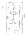
- FIG. 3A more detailed schematic of a typical DC-DC converter 24 is illustrated in FIG. 3 .
- the DC-DC converteris, in the illustrated embodiment, a Buck converter 24 A.
- the Buck converter 24 Aincludes an oscillator (OSC) 36 , a converter control system 38 , and a power train 40 .
- the converter control system 38in this example includes an error amplifier 42 and a modulator 44 .
- the oscillator 36outputs a saw-tooth voltage waveform derived from the voltage on an internal capacitor (not illustrated). In the example, the saw-tooth wave form ramps up and ramps down. Other oscillators 36 may provide a ramp up followed by a rapid return. Regardless of the particular wave form, the voltage is fed to the modulator 44 where it is compared to an error voltage signal 46 from the error amplifier 42 .
- the converter control system 38operates according to a pulse width modulation scheme as is well understood, although other arrangements are possible and applicable to the present invention.
- the error amplifier 42 of the converter control system 38compares a feedback signal 48 to a voltage reference (VREF 1 ) and generates the error voltage signal 46 .
- the feedback signal 48may be conditioned by phase compensation circuitry 49 for stability purposes.
- the error voltage signal 46provides the threshold level used by the modulator 44 in processing the signal from the oscillator 36 to generate a signal 50 . When the signal from the oscillator 36 is above the threshold determined by the error voltage signal 46 , the signal 50 provided to the power train 40 is low.
- the power train 40receives a high signal.
- the signal 50 driving the power train 40is a square wave with a duty cycle determined by the level of the error voltage signal.
- the power train 40includes an inductor 52 , a capacitor 54 , plus two switches 56 , 58 .
- the switches 56 , 58are, in the illustrated embodiment a p-channel FET and an N-channel FET respectively as is well understood for a typical buck topology.
- the square wave signal 50turns the switches 56 , 58 on and off. When the signal 50 is low, switch 56 is ON and switch 58 is OFF. This presents a voltage close to the voltage from the battery 20 to the inductor 52 causing an increase in current and storing energy in the inductor 52 's magnetic field. Current is supplied to the power amplifier 22 and to the capacitor 54 . When the signal 50 is high, switch 56 is OFF and switch 58 is ON.
- the present inventionlies in the oscillator 36 and is illustrated variously in FIGS. 4 , 6 , 8 , and 10 with accompanying flow charts in FIGS. 5A , 5 B, 7 A, 7 B, 9 A, 9 B, 11 A, and 11 B.
- the present inventionperiodically varies the frequency at which the oscillator 36 operates thus periodically changing the frequency of any ripple that appears in Vcc. Since the frequency of the ripple changes, the location in the frequency spectrum of the spurs changes. By moving the location of the spurs in the frequency spectrum, the energy at any given frequency is reduced, thereby helping meet the side band emissions requirements.
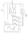
- the oscillator 36includes a pseudo random number generator 60 and a clock generation circuit 62 .
- the pseudo random number generator 60includes a seven bit shift register 64 with a most significant bit (MSB) output 66 and a least significant bit (LSB) output 68 .
- Two outputs(which in the exemplary embodiment are the MSB output 66 and the next most significant bit output 70 ) are directed to an exclusive OR (XOR) gate 72 .
- the output of the XOR gate 72is fed back into an input of the shift register 64 , thereby causing the shift register 64 to count in a pseudo random fashion and thus output a pseudo random number.
- Thisis known as a linear feedback shift register (LFSR) and is well known in the art.
- LFSRlinear feedback shift register
- Other pseudo random number generators 60could also be used if needed or desired.
- the number of bits in the shift registermay vary from embodiment to embodiment as needed or desired.
- the clock generation circuit 62includes a first digital to analog converter (DAC) 74 and a second digital to analog converter (DAC) 76 .
- the DACs 74 , 76translate the digital signal from the pseudo random number generator 60 into an analog setting that controls variable current sources 78 , 80 respectively. That is, the amount of current that flows through the current sources 78 , 80 is varied by the DACs 74 , 76 .
- the current sources 78 , 80are selectively connected to a capacitor C 1 by a switch 82 .
- the first current source 78is connected to a reference voltage supply (VREF 2 ) 84 and thus provides current to the capacitor C 1 when connected thereto, while the second current source 80 is connected to ground and thus acts as a current sink for the capacitor C 1 when connected thereto.
- VREF 2reference voltage supply
- a voltageis present at node 86 corresponding to the charge on the capacitor C 1 .
- the voltage at node 86has a saw tooth voltage waveform due to the current that flows into and out of the capacitor C 1 .
- This voltage at node 86is presented to comparators 88 , 90 .
- First comparator 88compares the voltage at node 86 to a predefined voltage level Vtop and second comparator 90 compares the voltage at node 86 to a predefined voltage level Vbot. If the voltage at node 86 exceeds Vtop, the first comparator 88 sends a signal to a flip-flop 92 . If the voltage at node 86 dips below Vbot, the second comparator 90 sends a signal to the flip-flop 92 .
- the act of sending a signal to the flip-flop 92 from either comparator 88 or 90causes a clock pulse (CLK 1 ) to be output by the flip-flop 92 .
- This clock pulsecontrols the switch 82 and is further directed to a divide by N element (/N) 94 .
- the divide by N element 94may have a counter which counts the pulses received in CLK 1 and determines if N pulses have been received. Once N pulses have been received, the divide by N element 94 outputs a pulse (CLK 2 ) which is received by the shift register 64 at clock input (CLK 2 ) 96 .
- CLK 2clock input
- the divide by N element 94effectively divides CLK 1 by N to arrive at CLK 2 .
- the receipt of the CLK 2 signalcauses the shift register to perform a “count” and change the pseudo random number being output.
- the value of N in the divide by N element 94is such that the pseudo random number output by the shift register changes approximately once every four milliseconds. Since a clock pulse is usually emitted from the flip-flop 92 approximately every four microseconds, N is in the neighborhood of 1000. Having the pseudo random number change approximately once every four milliseconds happens to correspond to the frequency of the transmission bursts in the GSM protocol and the measurement standard propounded under the GSM protocol. Likewise, this time period allows the transient response of the DC-DC converter 24 to settle between changes of the pseudo random number.
- a signal derived from the capacitor voltage 86is sent from the oscillator 36 to the converter control system 38 as needed or determined by the converter control system 38 .
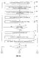
- FIGS. 5A and 5BA flow chart of the present invention in use is presented in FIGS. 5A and 5B .
- the processis continuous as long as the mobile terminal 10 is in the transmit mode, so the choice of a starting point is arbitrary. However, for the purposes of explanation, the process begins when the shift register 64 receives a CLK 2 signal at the clock input 96 (block 100 ) in FIG. 5A .
- the shift register 64increments the count to a new pseudo random number (block 102 ).
- the new pseudo random numbersets the DACs 74 , 76 and thus the current level through the current sources 78 , 80 (block 104 ).
- the switch 82moves to the current source 78 (block 106 ).
- the capacitor C 1charges based on the DAC 74 setting (block 108 ).
- the comparator 88determines if the voltage on the capacitor C 1 as measured at node 86 is greater than Vtop (block 110 ). If the answer is no, the capacitor C 1 continues to charge. If the answer is yes, the comparator 88 sets the flip-flop 92 (block 112 ). As a result of the signal to the flip-flop 92 , the flip-flop 92 generates a CLK 2 signal (block 114 ).
- the CLK 2 signal from the flip-flop 92moves the switch 82 to the current source 80 which sinks current (block 116 ).
- the CLK 2 signal from the flip-flop 92also travels to the divide by N element 94 .
- the divide by N element 94determines if the number of pulses in the CLK 2 signal since the last change in the pseudo random number divided by N is greater than 1 (block 118 ). If the answer is yes, N pulses have been received by the divide by N element 94 since the last change in the pseudo random number, the divide by N element 94 sends a CLK 2 signal to the clock input 96 of the shift register 64 , and the process repeats.
- the comparator 90determines if the voltage on the capacitor C 1 as measured at node 86 is less than Vbot (block 122 ). If the answer is no, the capacitor C 1 continues to discharge. If the answer is yes, the comparator 90 resets the flip-flop 92 (block 124 ). As a result of the signal to the flip-flop 92 , the flip-flop 92 generates a CLK 2 signal (block 126 ). The CLK 2 signal moves the switch 82 to the current source 78 (block 128 ). The CLK 2 signal from the flip-flop 92 also travels to the divide by N element 94 .
- the divide by N element 94determines if the number of pulses in the CLK 2 signal since the last change in the pseudo random number divided by N is greater than 1 (block 130 ). If the answer is yes, N pulses have been received by the divide by N element 94 since the last change in the pseudo random number, the divide by N element 94 sends a CLK 2 signal to the clock input 96 of the shift register 64 and the process repeats. If however, the answer to block 130 is no, fewer than N pulses have been received by divide by N element 94 since the last change in pseudo random number, then divide by N element 94 increments a count and the capacitor C 1 charges based on the setting for first DAC 74 (block 108 ) ( FIG. 5A ).
- the pseudo random number generator 60may take a number of different forms.
- the clock generation circuit 62may take a number of different forms. Other embodiments of the clock generation circuit 62 are set forth below.
- the pseudo random number generator (PNG) 60outputs the pseudo random number, which in turn controls switches 152 , 154 , 156 .
- the switches 152 , 154 , 156selectively activate capacitors C 2 , C 3 , and C 4 respective to node 158 .
- the pseudo random number output by the pseudo random number generator 60maps which capacitors are activated.
- the pseudo random number generator 60used a seven bit register, there might be seven capacitors, with each bit mapping to a capacitor.
- a varactorcould be used in place of a plurality of capacitors, and the amount of capacitance would be set by the pseudo random number.
- the capacitors C 2 , C 3 , and C 4may be physically connected to the node regardless of the position of the switches 152 , 154 , 156 , but the capacitors C 2 , C 3 , and C 4 are effectively open circuits until the switches 152 , 154 , and 156 are closed.
- “activate” or “activated”means that the corresponding switch is closed and the capacitor completes a circuit.
- Node 158acts like the node 86 in the first embodiment and is the point from which measurements are made by comparators 88 , 90 to trigger the flip-flop 92 .
- the saw-tooth signal at node 158may be used by the modulator 44 ( FIG. 3 ).
- the flip-flop 92generates the CLK 2 signal as previously described which may go to a divide by N element (not shown in FIG. 6 ) and a switch 160 .
- the switch 160selectively connects the node 158 to one of the current sources 162 or 164 .
- the current source 162charges the capacitors that are activated by the switches 152 , 154 , 156 when the current source 162 is connected to node 158 by the switch 160 .
- the current source 164discharges the capacitors C 2 , C 3 , and C 4 that are activated when the current source 164 is connected to node 158 by the switch 160 .
- this embodimentvaries the capacitance as a function of the output of the pseudo random number generator 60 . Varying the capacitance effectively changes the period of the charging and discharging as effectively as changing the current levels that do the charging and discharging.
- FIGS. 7A and 7BA flow chart illustrating the functionality of the second embodiment is presented in FIGS. 7A and 7B . Again, because of the continuous nature of the process, the starting point is somewhat arbitrary.
- the pseudo random number generator (PNG) 60outputs a new pseudo random number (PN) (block 200 ).
- the PNdetermines which of the capacitors are activated, and the switches 152 , 154 , 156 are opened or closed based on the PN (block 202 ).
- the switch 160also moves to complete the circuit with the current source 162 (block 204 ). The current flows through the current source 162 into the activated capacitors, and the activated capacitors charge (block 206 ).
- the voltage at node 158is presented to the comparators 88 and 90 and a determination is made as to whether the voltage at node 158 is greater than Vtop (block 208 ). If the answer is no, the activated capacitors continue to charge. If the answer to block 208 is yes, the voltage at node 158 is greater than Vtop, then the comparator 88 sets the flip-flop 92 (block 210 ). The flip-flop 92 generates a pulse in the CLK 2 signal (block 212 ). The CLK 2 signal pulse causes the switch 160 to move to current source 164 (block 214 ). The current source 164 draws current out of the activated capacitors and the activated capacitors discharge (block 216 ).
- the comparator 90determines if the voltage at node 158 is less than Vbot (block 218 ). If the answer is no, the capacitors continue to discharge. If the answer to block 218 is yes, the voltage at node 158 has dropped below Vbot, then the comparator 90 resets the flip-flop 92 (block 220 ) as illustrated in FIG. 7B . The flip-flop generates a pulse in the CLK 2 signal (block 222 ).
- a determinationmay be made as to whether it is time to change the PN (block 224 ). This may be done through the divide by N element 94 (not shown in FIG. 6 ) or other technique as needed or desired. Further, the determination may be made at various locations in the flow chart, although only one is illustrated. In the embodiment illustrated, if the determination is negative, then the switch 160 is moved to current source 162 (block 204 ) and the process continues; otherwise, a new PN may be generated (block 200 ).
- a third embodimentis illustrated in FIG. 8 .
- the PNG 60outputs a pseudo random number to a DAC 250 that in turn controls a variable current source 252 .
- the variable current source 252outputs a current that is mirrored from a first Field Effect Transistor (FET) 254 to a second FET 256 and a third FET 258 .
- FETField Effect Transistor
- the current mirrored into the second FET 256forces a current to exist in a fourth FET 260 .
- the current in the fourth FET 260is mirrored into a fifth FET 262 . While FETs are illustrated, other current mirroring mechanisms could also be used.
- the third FET 258acts as a current sink and the fifth FET 262 acts as a current source for the capacitor C 1 depending on the position of the switch 264 .
- This embodimenthas the advantage of taking up less space in a semiconductor than the two DAC arrangement of FIG. 4 , but at the expense of wasted current.
- the comparators 88 , 90measure the voltage at node 266 and set and reset the flip-flop 92 much as previously described.
- the flip-flop 92generates a CLK 2 signal, whose pulses move the switch 264 and periodically cause a new pseudo random number to be generated by the PNG 60 .
- the saw-tooth signal on the capacitor C 1 at node 266may be used by the modulator 44 ( FIG. 3 ) as previously explained.
- FIGS. 9A and 9BA flow chart of the operation of the embodiment of FIG. 8 appears in FIGS. 9A and 9B .
- the pseudo random number generator (PNG)outputs a new pseudo random number (PN) (block 300 ).
- the DAC 250receives the PN and sets the current level for the variable current source 252 (block 302 ).
- the currentpasses through the current source 252 and is mirrored about by the various FETs (block 304 ).
- the switch 264moves to FET 262 (block 306 ).
- the capacitor C 1charges (block 308 ).
- the comparator 88determines if the voltage at node 266 is greater than Vtop (block 310 ). If the answer to the inquiry at block 310 is no, then the capacitor C 1 continues to charge. If the answer to the inquiry at block 310 is yes, the voltage at node 266 is greater than Vtop, then the comparator 88 sets the flip-flop 92 (block 312 ). The flip-flop 92 generates a pulse in the CLK 2 signal (block 314 ).
- the pulse in the CLK 2 signalcauses the switch 264 to move to the FET 258 (block 316 ).
- the capacitor C 1now discharges through FET 258 (block 318 ) as illustrated in FIG. 9B .
- the comparator 90determines if the voltage at node 266 is less than Vbot (block 320 ). If the answer to the inquiry at block 320 is no, then the capacitor C 1 continues to discharge. If, however, the answer to the inquiry at block 320 is yes, the voltage at node 266 is less than Vbot, then the comparator 90 resets the flip-flop 92 (block 322 ).
- the flip-flop 92generates a pulse in the CLK 2 signal (block 324 ). It should be appreciated that periodically a determination may be made as to whether it is time to change the PN (block 326 ). This may be done through the divide by N element 94 (not shown in FIG. 8 ) or other technique as needed or desired. Further, the determination may be made at various locations in the flow chart, although only one is illustrated. In the embodiment illustrated, if the determination is negative, then the switch 264 may move to the FET 262 (block 306 ) and the capacitor C 1 charges (block 308 ); otherwise, a new PN may be generated (block 300 ).
- a fourth embodimentis illustrated in FIG. 10 .
- the PNG 60outputs a pseudo random number that is passed to a DAC 350 .
- the DAC 350controls a variable current source 352 that alternately charges two capacitors C 5 and C 6 .
- a comparator 354compares VREF to the voltage at node 356 .
- the voltage at node 356is set by the position of the switch 358 and the positions of the switches 360 , 362 .
- the comparator 354outputs a signal to the flip-flop 92 which generates a CLK 2 signal for use by the PNG 60 .
- the saw-tooth voltage at node 356may be used by the modulator 44 ( FIG. 3 ) as previously explained.
- C 6is charging from the variable current source 352 and C 5 is discharging.
- C 5is charging and C 6 is discharging.
- the position of switch 358determines if the voltage at node 356 is the voltage on C 5 or the voltage on C 6 .
- the flip-flop 92 and the state thereofcontrol the switch settings for the switches 358 , 360 , and 362 .
- the voltage seen by the comparator 354is a rising ramp followed by a rapid drop as the other discharged capacitor is switched in and then a rising ramp as that capacitor is charged. Note that this circuit may need a start-up or watch dog monitor since a non-oscillating mode does exist.
- the functionality of the embodiment of FIG. 10is set forth as a flow chart in FIGS. 11A and 11B .
- the PNG 60outputs a new PN (block 400 ).
- the DAC 350receives the PN and sets the current level of the variable current source 352 (block 402 ). Current flows through the variable current source 352 to the capacitor C 6 (block 404 ). The capacitor C 6 charges (block 406 ). Meanwhile, the switch 362 closes the loop for capacitor C 5 , and capacitor C 5 discharges (block 408 ).
- the comparator 354determines if the voltage at node 356 is greater than VREF (block 410 ). If the answer is no, then the capacitor C 6 continues to charge and the capacitor C 5 continues to discharge. If, however, the answer to the inquiry at block 410 is yes, the voltage at node 356 is greater than VREF, then the comparator 354 clocks the flip-flop 92 (block 412 ). The flip-flop 92 generates a pulse in the CLK 2 signal (block 414 ). Further, the flip-flop 92 toggles the switches 358 , 360 , 362 (block 416 ).
- the comparatordetermines if the voltage at node 356 is greater than VREF (block 424 ). If the answer is no, then the capacitor C 5 continues to charge (block 420 ). If the answer to the inquiry at block 424 is yes, then the comparator clocks the flip-flop 92 (block 426 ). The flip-flop 92 generates a pulse in the CLK 2 signal (block 428 ) and toggles the switches 358 , 360 , and 362 (block 430 ).
- a determinationmay be made as to whether it is time to change the PN (block 432 ). This may be done through the divide by N element 94 (not shown in FIG. 10 ) or other technique as needed or desired. Further, the determination may be made at various locations in the flow chart, although only one is illustrated. If it is not time for a new PN, the process repeats from block 404 . If it is time for a new PN, the process repeats from block 400 .
- comparators 88 , 90are used throughout the exemplary embodiments, it is also possible to use inverter gates therefore.
- the ratio of the top and bottom transistor sizemay be skewed to change the logic threshold.
Landscapes
- Engineering & Computer Science (AREA)
- Computer Networks & Wireless Communication (AREA)
- Signal Processing (AREA)
- Power Engineering (AREA)
- Dc-Dc Converters (AREA)
- Noise Elimination (AREA)
Abstract
Description
Claims (14)
Priority Applications (3)
| Application Number | Priority Date | Filing Date | Title |
|---|---|---|---|
| US10/389,849US6969978B2 (en) | 2003-03-17 | 2003-03-17 | DC-DC converter with reduced electromagnetic interference |
| EP04719717.3AEP1604446B1 (en) | 2003-03-17 | 2004-03-11 | Dc-dc converter with reduced electromagnetic interference |
| PCT/US2004/007307WO2004084392A2 (en) | 2003-03-17 | 2004-03-11 | Dc-dc converter with reduced electromagnetic interference |
Applications Claiming Priority (1)
| Application Number | Priority Date | Filing Date | Title |
|---|---|---|---|
| US10/389,849US6969978B2 (en) | 2003-03-17 | 2003-03-17 | DC-DC converter with reduced electromagnetic interference |
Publications (2)
| Publication Number | Publication Date |
|---|---|
| US20040183511A1 US20040183511A1 (en) | 2004-09-23 |
| US6969978B2true US6969978B2 (en) | 2005-11-29 |
Family
ID=32987446
Family Applications (1)
| Application Number | Title | Priority Date | Filing Date |
|---|---|---|---|
| US10/389,849Expired - LifetimeUS6969978B2 (en) | 2003-03-17 | 2003-03-17 | DC-DC converter with reduced electromagnetic interference |
Country Status (3)
| Country | Link |
|---|---|
| US (1) | US6969978B2 (en) |
| EP (1) | EP1604446B1 (en) |
| WO (1) | WO2004084392A2 (en) |
Cited By (123)
| Publication number | Priority date | Publication date | Assignee | Title |
|---|---|---|---|---|
| US20050206361A1 (en)* | 2004-03-17 | 2005-09-22 | Denso Corporation | DC-DC converter for boosting input voltage at variable frequency |
| US20050243581A1 (en)* | 2004-04-30 | 2005-11-03 | Franz-Otto Witte | Direct current voltage transformer |
| US20060119422A1 (en)* | 2004-11-02 | 2006-06-08 | Satoshi Sakurai | Semiconductor device including current control circuit of reference current source |
| US20060152953A1 (en)* | 2005-01-10 | 2006-07-13 | Sangbeom Park | Variable start-up circuit for switching regulators |
| US20060255812A1 (en)* | 2005-05-06 | 2006-11-16 | Agere Systems Incorporated | Low-power switch state detection circuit and method and mobile telephone device incorporating the same |
| US20070139105A1 (en)* | 2005-06-10 | 2007-06-21 | Rf Micro Devices, Inc. | Doherty amplifier configuration for a collector controlled power amplifier |
| US20070170931A1 (en)* | 2006-01-20 | 2007-07-26 | Snyder Warren S | Successive approximate capacitance measurement circuit |
| US7253643B1 (en) | 2006-07-19 | 2007-08-07 | Cypress Semiconductor Corporation | Uninterrupted radial capacitive sense interface |
| US7307485B1 (en)* | 2005-11-14 | 2007-12-11 | Cypress Semiconductor Corporation | Capacitance sensor using relaxation oscillators |
| US7330071B1 (en) | 2005-10-19 | 2008-02-12 | Rf Micro Devices, Inc. | High efficiency radio frequency power amplifier having an extended dynamic range |
| US20080157831A1 (en)* | 2006-12-28 | 2008-07-03 | Taiwan Semiconductor Manufacturing Co., Ltd. | Clock generation with reduced electromagnetic interference for DC-DC converters |
| US20080157894A1 (en)* | 2005-04-26 | 2008-07-03 | Dan Ion Hariton | Method and apparatus for frequency modulating a periodic signal of varying duty cycle |
| US20090009194A1 (en)* | 2007-07-03 | 2009-01-08 | Cypress Semiconductor Corporation | Normalizing capacitive sensor array signals |
| US7721609B2 (en) | 2006-03-31 | 2010-05-25 | Cypress Semiconductor Corporation | Method and apparatus for sensing the force with which a button is pressed |
| US7737724B2 (en) | 2007-04-17 | 2010-06-15 | Cypress Semiconductor Corporation | Universal digital block interconnection and channel routing |
| US7761845B1 (en) | 2002-09-09 | 2010-07-20 | Cypress Semiconductor Corporation | Method for parameterizing a user module |
| US7765095B1 (en) | 2000-10-26 | 2010-07-27 | Cypress Semiconductor Corporation | Conditional branching in an in-circuit emulation system |
| US7770113B1 (en) | 2001-11-19 | 2010-08-03 | Cypress Semiconductor Corporation | System and method for dynamically generating a configuration datasheet |
| US7774190B1 (en) | 2001-11-19 | 2010-08-10 | Cypress Semiconductor Corporation | Sleep and stall in an in-circuit emulation system |
| US20100253305A1 (en)* | 2007-03-12 | 2010-10-07 | Melanson John L | Switching power converter control with spread spectrum based electromagnetic interference reduction |
| US7825688B1 (en) | 2000-10-26 | 2010-11-02 | Cypress Semiconductor Corporation | Programmable microcontroller architecture(mixed analog/digital) |
| US7844437B1 (en) | 2001-11-19 | 2010-11-30 | Cypress Semiconductor Corporation | System and method for performing next placements and pruning of disallowed placements for programming an integrated circuit |
| US7893724B2 (en) | 2004-03-25 | 2011-02-22 | Cypress Semiconductor Corporation | Method and circuit for rapid alignment of signals |
| US7928712B1 (en)* | 2007-06-01 | 2011-04-19 | Rf Micro Devices, Inc. | Low noise fast dithering switching power supply |
| US20110095734A1 (en)* | 2007-01-22 | 2011-04-28 | Power Integrations, Inc. | Cascaded pfc and resonant mode power converters |
| US20110134670A1 (en)* | 2007-01-22 | 2011-06-09 | Power Integrations, Inc. | Control arrangement for a pfc power converter |
| US8026739B2 (en) | 2007-04-17 | 2011-09-27 | Cypress Semiconductor Corporation | System level interconnect with programmable switching |
| US8040321B2 (en) | 2006-07-10 | 2011-10-18 | Cypress Semiconductor Corporation | Touch-sensor with shared capacitive sensors |
| US8040266B2 (en) | 2007-04-17 | 2011-10-18 | Cypress Semiconductor Corporation | Programmable sigma-delta analog-to-digital converter |
| US8040142B1 (en) | 2006-03-31 | 2011-10-18 | Cypress Semiconductor Corporation | Touch detection techniques for capacitive touch sense systems |
| US8049569B1 (en) | 2007-09-05 | 2011-11-01 | Cypress Semiconductor Corporation | Circuit and method for improving the accuracy of a crystal-less oscillator having dual-frequency modes |
| US8058937B2 (en) | 2007-01-30 | 2011-11-15 | Cypress Semiconductor Corporation | Setting a discharge rate and a charge rate of a relaxation oscillator circuit |
| US8069428B1 (en) | 2001-10-24 | 2011-11-29 | Cypress Semiconductor Corporation | Techniques for generating microcontroller configuration information |
| US8069436B2 (en) | 2004-08-13 | 2011-11-29 | Cypress Semiconductor Corporation | Providing hardware independence to automate code generation of processing device firmware |
| US8069405B1 (en) | 2001-11-19 | 2011-11-29 | Cypress Semiconductor Corporation | User interface for efficiently browsing an electronic document using data-driven tabs |
| US8067948B2 (en) | 2006-03-27 | 2011-11-29 | Cypress Semiconductor Corporation | Input/output multiplexer bus |
| US8078894B1 (en) | 2007-04-25 | 2011-12-13 | Cypress Semiconductor Corporation | Power management architecture, method and configuration system |
| US8078970B1 (en) | 2001-11-09 | 2011-12-13 | Cypress Semiconductor Corporation | Graphical user interface with user-selectable list-box |
| US8085067B1 (en) | 2005-12-21 | 2011-12-27 | Cypress Semiconductor Corporation | Differential-to-single ended signal converter circuit and method |
| US8085100B2 (en) | 2005-02-04 | 2011-12-27 | Cypress Semiconductor Corporation | Poly-phase frequency synthesis oscillator |
| US8089289B1 (en) | 2007-07-03 | 2012-01-03 | Cypress Semiconductor Corporation | Capacitive field sensor with sigma-delta modulator |
| US8089288B1 (en) | 2006-11-16 | 2012-01-03 | Cypress Semiconductor Corporation | Charge accumulation capacitance sensor with linear transfer characteristic |
| US8089472B2 (en) | 2006-05-26 | 2012-01-03 | Cypress Semiconductor Corporation | Bidirectional slider with delete function |
| US8089461B2 (en) | 2005-06-23 | 2012-01-03 | Cypress Semiconductor Corporation | Touch wake for electronic devices |
| US8092083B2 (en) | 2007-04-17 | 2012-01-10 | Cypress Semiconductor Corporation | Temperature sensor with digital bandgap |
| US8103496B1 (en) | 2000-10-26 | 2012-01-24 | Cypress Semicondutor Corporation | Breakpoint control in an in-circuit emulation system |
| US8103497B1 (en) | 2002-03-28 | 2012-01-24 | Cypress Semiconductor Corporation | External interface for event architecture |
| US8120408B1 (en) | 2005-05-05 | 2012-02-21 | Cypress Semiconductor Corporation | Voltage controlled oscillator delay cell and method |
| US8130025B2 (en) | 2007-04-17 | 2012-03-06 | Cypress Semiconductor Corporation | Numerical band gap |
| US8144126B2 (en) | 2007-05-07 | 2012-03-27 | Cypress Semiconductor Corporation | Reducing sleep current in a capacitance sensing system |
| US8145149B2 (en) | 2010-06-17 | 2012-03-27 | R2 Semiconductor, Inc | Operating a voltage regulator at a switching frequency selected to reduce spurious signals |
| US8149048B1 (en) | 2000-10-26 | 2012-04-03 | Cypress Semiconductor Corporation | Apparatus and method for programmable power management in a programmable analog circuit block |
| US8160864B1 (en) | 2000-10-26 | 2012-04-17 | Cypress Semiconductor Corporation | In-circuit emulator and pod synchronized boot |
| US8169238B1 (en) | 2007-07-03 | 2012-05-01 | Cypress Semiconductor Corporation | Capacitance to frequency converter |
| US8176296B2 (en) | 2000-10-26 | 2012-05-08 | Cypress Semiconductor Corporation | Programmable microcontroller architecture |
| US20120161728A1 (en)* | 2010-12-27 | 2012-06-28 | Analog Devices, Inc. | Switching voltage regulators with hysteretic control for enhanced mode-transition speed and stability |
| US8248051B2 (en) | 2008-06-19 | 2012-08-21 | Power Integrations, Inc. | Power factor correction converter control offset |
| US8274799B2 (en) | 2007-01-22 | 2012-09-25 | Power Integrations, Inc. | Control arrangement for a resonant mode power converter |
| US8286125B2 (en) | 2004-08-13 | 2012-10-09 | Cypress Semiconductor Corporation | Model for a hardware device-independent method of defining embedded firmware for programmable systems |
| US8321174B1 (en) | 2008-09-26 | 2012-11-27 | Cypress Semiconductor Corporation | System and method to measure capacitance of capacitive sensor array |
| US8358142B2 (en) | 2008-02-27 | 2013-01-22 | Cypress Semiconductor Corporation | Methods and circuits for measuring mutual and self capacitance |
| US8402313B1 (en) | 2002-05-01 | 2013-03-19 | Cypress Semiconductor Corporation | Reconfigurable testing system and method |
| CN101657958B (en)* | 2007-01-22 | 2013-05-22 | 电力集成公司 | Control Arrangement for Resonant Mode Power Converter |
| US8487912B1 (en) | 2008-02-01 | 2013-07-16 | Cypress Semiconductor Corporation | Capacitive sense touch device with hysteresis threshold |
| US8487639B1 (en) | 2008-11-21 | 2013-07-16 | Cypress Semiconductor Corporation | Receive demodulator for capacitive sensing |
| US8493351B2 (en) | 2006-03-30 | 2013-07-23 | Cypress Semiconductor Corporation | Apparatus and method for reducing average scan rate to detect a conductive object on a sensing device |
| US8515361B2 (en) | 2010-04-20 | 2013-08-20 | Rf Micro Devices, Inc. | Frequency correction of a programmable frequency oscillator by propagation delay compensation |
| US8525798B2 (en) | 2008-01-28 | 2013-09-03 | Cypress Semiconductor Corporation | Touch sensing |
| US8533677B1 (en) | 2001-11-19 | 2013-09-10 | Cypress Semiconductor Corporation | Graphical user interface for dynamically reconfiguring a programmable device |
| US8538355B2 (en) | 2010-04-19 | 2013-09-17 | Rf Micro Devices, Inc. | Quadrature power amplifier architecture |
| US8537121B2 (en) | 2006-05-26 | 2013-09-17 | Cypress Semiconductor Corporation | Multi-function slider in touchpad |
| US8542061B2 (en) | 2010-04-20 | 2013-09-24 | Rf Micro Devices, Inc. | Charge pump based power amplifier envelope power supply and bias power supply |
| US8559898B2 (en) | 2010-04-20 | 2013-10-15 | Rf Micro Devices, Inc. | Embedded RF PA temperature compensating bias transistor |
| US8565694B2 (en) | 2010-04-20 | 2013-10-22 | Rf Micro Devices, Inc. | Split current current digital-to-analog converter (IDAC) for dynamic device switching (DDS) of an RF PA stage |
| US8570052B1 (en) | 2008-02-27 | 2013-10-29 | Cypress Semiconductor Corporation | Methods and circuits for measuring mutual and self capacitance |
| US8570053B1 (en) | 2007-07-03 | 2013-10-29 | Cypress Semiconductor Corporation | Capacitive field sensor with sigma-delta modulator |
| US8571492B2 (en) | 2010-04-20 | 2013-10-29 | Rf Micro Devices, Inc. | DC-DC converter current sensing |
| US8699973B2 (en) | 2010-04-20 | 2014-04-15 | Rf Micro Devices, Inc. | PA bias power supply efficiency optimization |
| US8706063B2 (en) | 2010-04-20 | 2014-04-22 | Rf Micro Devices, Inc. | PA envelope power supply undershoot compensation |
| US8712349B2 (en) | 2010-04-20 | 2014-04-29 | Rf Micro Devices, Inc. | Selecting a converter operating mode of a PA envelope power supply |
| US8731498B2 (en) | 2010-04-20 | 2014-05-20 | Rf Micro Devices, Inc. | Temperature correcting an envelope power supply signal for RF PA circuitry |
| US8811920B2 (en) | 2010-04-20 | 2014-08-19 | Rf Micro Devices, Inc. | DC-DC converter semiconductor die structure |
| US8811921B2 (en) | 2010-04-20 | 2014-08-19 | Rf Micro Devices, Inc. | Independent PA biasing of a driver stage and a final stage |
| US8831544B2 (en) | 2010-04-20 | 2014-09-09 | Rf Micro Devices, Inc. | Dynamic device switching (DDS) of an in-phase RF PA stage and a quadrature-phase RF PA stage |
| US8842399B2 (en) | 2010-04-20 | 2014-09-23 | Rf Micro Devices, Inc. | ESD protection of an RF PA semiconductor die using a PA controller semiconductor die |
| US8854019B1 (en) | 2008-09-25 | 2014-10-07 | Rf Micro Devices, Inc. | Hybrid DC/DC power converter with charge-pump and buck converter |
| US8866500B2 (en) | 2009-03-26 | 2014-10-21 | Cypress Semiconductor Corporation | Multi-functional capacitance sensing circuit with a current conveyor |
| US8874050B1 (en) | 2009-05-05 | 2014-10-28 | Rf Micro Devices, Inc. | Saturation correction without using saturation detection and saturation prevention for a power amplifier |
| US8892063B2 (en) | 2010-04-20 | 2014-11-18 | Rf Micro Devices, Inc. | Linear mode and non-linear mode quadrature PA circuitry |
| US8913971B2 (en) | 2010-04-20 | 2014-12-16 | Rf Micro Devices, Inc. | Selecting PA bias levels of RF PA circuitry during a multislot burst |
| US8913967B2 (en) | 2010-04-20 | 2014-12-16 | Rf Micro Devices, Inc. | Feedback based buck timing of a direct current (DC)-DC converter |
| US8942650B2 (en) | 2010-04-20 | 2015-01-27 | Rf Micro Devices, Inc. | RF PA linearity requirements based converter operating mode selection |
| US8942651B2 (en) | 2010-04-20 | 2015-01-27 | Rf Micro Devices, Inc. | Cascaded converged power amplifier |
| US8947157B2 (en) | 2010-04-20 | 2015-02-03 | Rf Micro Devices, Inc. | Voltage multiplier charge pump buck |
| US8958763B2 (en) | 2010-04-20 | 2015-02-17 | Rf Micro Devices, Inc. | PA bias power supply undershoot compensation |
| US8983410B2 (en) | 2010-04-20 | 2015-03-17 | Rf Micro Devices, Inc. | Configurable 2-wire/3-wire serial communications interface |
| US8983407B2 (en) | 2010-04-20 | 2015-03-17 | Rf Micro Devices, Inc. | Selectable PA bias temperature compensation circuitry |
| US8989685B2 (en) | 2010-04-20 | 2015-03-24 | Rf Micro Devices, Inc. | Look-up table based configuration of multi-mode multi-band radio frequency power amplifier circuitry |
| US9008597B2 (en) | 2010-04-20 | 2015-04-14 | Rf Micro Devices, Inc. | Direct current (DC)-DC converter having a multi-stage output filter |
| US9020452B2 (en) | 2010-02-01 | 2015-04-28 | Rf Micro Devices, Inc. | Envelope power supply calibration of a multi-mode radio frequency power amplifier |
| US9030256B2 (en) | 2010-04-20 | 2015-05-12 | Rf Micro Devices, Inc. | Overlay class F choke |
| US9048787B2 (en) | 2010-04-20 | 2015-06-02 | Rf Micro Devices, Inc. | Combined RF detector and RF attenuator with concurrent outputs |
| US9065505B2 (en) | 2012-01-31 | 2015-06-23 | Rf Micro Devices, Inc. | Optimal switching frequency for envelope tracking power supply |
| US9077405B2 (en) | 2010-04-20 | 2015-07-07 | Rf Micro Devices, Inc. | High efficiency path based power amplifier circuitry |
| US9154160B2 (en) | 2006-11-14 | 2015-10-06 | Cypress Semiconductor Corporation | Capacitance to code converter with sigma-delta modulator |
| US9166471B1 (en)* | 2009-03-13 | 2015-10-20 | Rf Micro Devices, Inc. | 3D frequency dithering for DC-to-DC converters used in multi-mode cellular transmitters |
| US9184701B2 (en) | 2010-04-20 | 2015-11-10 | Rf Micro Devices, Inc. | Snubber for a direct current (DC)-DC converter |
| US9214865B2 (en) | 2010-04-20 | 2015-12-15 | Rf Micro Devices, Inc. | Voltage compatible charge pump buck and buck power supplies |
| US9214900B2 (en) | 2010-04-20 | 2015-12-15 | Rf Micro Devices, Inc. | Interference reduction between RF communications bands |
| US9268441B2 (en) | 2011-04-05 | 2016-02-23 | Parade Technologies, Ltd. | Active integrator for a capacitive sense array |
| US9362825B2 (en) | 2010-04-20 | 2016-06-07 | Rf Micro Devices, Inc. | Look-up table based configuration of a DC-DC converter |
| US9417728B2 (en) | 2009-07-28 | 2016-08-16 | Parade Technologies, Ltd. | Predictive touch surface scanning |
| US9448964B2 (en) | 2009-05-04 | 2016-09-20 | Cypress Semiconductor Corporation | Autonomous control in a programmable system |
| US9500686B1 (en) | 2007-06-29 | 2016-11-22 | Cypress Semiconductor Corporation | Capacitance measurement system and methods |
| US9507465B2 (en) | 2006-07-25 | 2016-11-29 | Cypress Semiconductor Corporation | Technique for increasing the sensitivity of capacitive sensor arrays |
| US9553550B2 (en) | 2010-04-20 | 2017-01-24 | Qorvo Us, Inc. | Multiband RF switch ground isolation |
| US9564902B2 (en) | 2007-04-17 | 2017-02-07 | Cypress Semiconductor Corporation | Dynamically configurable and re-configurable data path |
| US9577590B2 (en) | 2010-04-20 | 2017-02-21 | Qorvo Us, Inc. | Dual inductive element charge pump buck and buck power supplies |
| US20170187286A1 (en)* | 2015-12-29 | 2017-06-29 | Texas Instruments Incorporated | Methods and Apparatus for a Low Standby Current DC-DC Power Controller with Improved Transient Response |
| US9766738B1 (en) | 2006-08-23 | 2017-09-19 | Cypress Semiconductor Corporation | Position and usage based prioritization for capacitance sense interface |
| US9900204B2 (en) | 2010-04-20 | 2018-02-20 | Qorvo Us, Inc. | Multiple functional equivalence digital communications interface |
| US20190115986A1 (en)* | 2017-10-18 | 2019-04-18 | Texas Instruments Incorporated | SWITCH MODE DIRECT CURRENT-TO-DIRECT CURRENT (DC-to-DC) CONVERTERS WITH REDUCED SPURIOUS NOISE EMISSION |
| US10656191B2 (en) | 2017-12-18 | 2020-05-19 | Microsoft Technology Licensing, Llc | Capacitance measuring circuit |
Families Citing this family (38)
| Publication number | Priority date | Publication date | Assignee | Title |
|---|---|---|---|---|
| US6701138B2 (en)* | 2001-06-11 | 2004-03-02 | Rf Micro Devices, Inc. | Power amplifier control |
| US7991071B2 (en) | 2002-05-16 | 2011-08-02 | Rf Micro Devices, Inc. | AM to PM correction system for polar modulator |
| US7801244B2 (en)* | 2002-05-16 | 2010-09-21 | Rf Micro Devices, Inc. | Am to AM correction system for polar modulator |
| US6998919B2 (en)* | 2003-10-22 | 2006-02-14 | Rf Micro Devices, Inc. | Temperature compensated power amplifier power control |
| US6980039B1 (en) | 2004-03-03 | 2005-12-27 | Rf Micro Devices, Inc. | DC-DC converter with noise spreading to meet spectral mask requirements |
| US7053713B1 (en) | 2004-06-02 | 2006-05-30 | Rf Micro Devices, Inc. | Multi-phase switching power supply having both voltage and current feedback loops |
| US7274748B1 (en) | 2004-06-02 | 2007-09-25 | Rf Micro Devices, Inc. | AM to FM correction system for a polar modulator |
| US7301400B1 (en) | 2004-06-02 | 2007-11-27 | Rf Micro Devices, Inc. | Multi-phase switching power supply for mobile telephone applications |
| US7551686B1 (en) | 2004-06-23 | 2009-06-23 | Rf Micro Devices, Inc. | Multiple polynomial digital predistortion |
| US7193459B1 (en) | 2004-06-23 | 2007-03-20 | Rf Micro Devices, Inc. | Power amplifier control technique for enhanced efficiency |
| US7109791B1 (en) | 2004-07-09 | 2006-09-19 | Rf Micro Devices, Inc. | Tailored collector voltage to minimize variation in AM to PM distortion in a power amplifier |
| US7132891B1 (en) | 2004-08-17 | 2006-11-07 | Rf Micro Devices, Inc. | Power amplifier control using a switching power supply |
| US7529523B1 (en) | 2004-08-23 | 2009-05-05 | Rf Micro Devices, Inc. | N-th order curve fit for power calibration in a mobile terminal |
| CN100525035C (en)* | 2004-11-16 | 2009-08-05 | 崇贸科技股份有限公司 | Switching control device with frequency hopping characteristic |
| US7167054B1 (en) | 2004-12-02 | 2007-01-23 | Rf Micro Devices, Inc. | Reconfigurable power control for a mobile terminal |
| CN100413191C (en) | 2005-03-30 | 2008-08-20 | 昂宝电子(上海)有限公司 | System and method for controlling switch frequency change in power supply transducer |
| US8224265B1 (en) | 2005-06-13 | 2012-07-17 | Rf Micro Devices, Inc. | Method for optimizing AM/AM and AM/PM predistortion in a mobile terminal |
| US7877060B1 (en) | 2006-02-06 | 2011-01-25 | Rf Micro Devices, Inc. | Fast calibration of AM/PM pre-distortion |
| US7962108B1 (en) | 2006-03-29 | 2011-06-14 | Rf Micro Devices, Inc. | Adaptive AM/PM compensation |
| US7689182B1 (en) | 2006-10-12 | 2010-03-30 | Rf Micro Devices, Inc. | Temperature compensated bias for AM/PM improvement |
| US8009762B1 (en) | 2007-04-17 | 2011-08-30 | Rf Micro Devices, Inc. | Method for calibrating a phase distortion compensated polar modulated radio frequency transmitter |
| EP2370125B1 (en)* | 2008-10-07 | 2019-04-10 | Roche Diabetes Care GmbH | Skin securable drug delivery device with a shock absorbing protective shield |
| US8489042B1 (en) | 2009-10-08 | 2013-07-16 | Rf Micro Devices, Inc. | Polar feedback linearization |
| TW201134079A (en)* | 2010-03-16 | 2011-10-01 | Noveltek Semiconductor Corp | Adjustable frequency generator and related power supply |
| JP5588219B2 (en)* | 2010-05-07 | 2014-09-10 | 株式会社東芝 | Clock generation circuit |
| CN102655706B (en)* | 2012-05-04 | 2015-03-11 | 成都芯源系统有限公司 | Light emitting element driver, control circuit and control method thereof |
| CN103929062B (en)* | 2013-01-11 | 2017-04-12 | 登丰微电子股份有限公司 | DC to DC power conversion circuit |
| US8786361B1 (en)* | 2013-03-08 | 2014-07-22 | Hamilton Sundstrand Corporation | High accuracy analog interface processing circuit |
| US9383761B2 (en)* | 2013-07-11 | 2016-07-05 | Texas Instruments Incorporated | Apparatus and method for multiphase SMPS interleaving |
| CN104638904B (en)* | 2013-11-06 | 2018-01-19 | 意法半导体研发(深圳)有限公司 | Peak-current mode DC DC converters |
| CN105610316A (en)* | 2015-08-14 | 2016-05-25 | 许继电源有限公司 | Frequency jittering circuit |
| US10110126B2 (en)* | 2015-09-04 | 2018-10-23 | Dailog Semiconductor (UK) Limited | Electromagnetic interference (EMI) for pulse frequency modulation (PFM) mode of a switching regulator |
| US10649477B2 (en) | 2017-05-18 | 2020-05-12 | Cypress Semiconductor Corporation | Programmable shunt regulator |
| US10541610B1 (en)* | 2018-08-21 | 2020-01-21 | Texas Instruments Incorporated | Spectral shaping of spread spectrum clocks/frequencies through post processing |
| US10361627B1 (en)* | 2018-09-12 | 2019-07-23 | Texas Instruments Incorporated | Reduction of low frequency noise in a discrete spread spectrum timebase |
| US11569838B2 (en) | 2020-04-09 | 2023-01-31 | Analog Devices International Unlimited Company | High efficiency current source/sink DAC |
| US11405026B2 (en) | 2020-08-12 | 2022-08-02 | Infineon Technologies LLC | Method and circuit for electromagnetic interference (EMI) reduction of analog blocks |
| US11206014B1 (en)* | 2021-04-27 | 2021-12-21 | High Tech Technology Limited | Digital frequency dithering for switched-mode power supplies (SMPS) using triangular, asymmetric cubic, or random cubic spread spectrum oscillators |
Citations (30)
| Publication number | Priority date | Publication date | Assignee | Title |
|---|---|---|---|---|
| US4064414A (en)* | 1977-01-31 | 1977-12-20 | Fbw Enterprises | Apparatus for simulating the light produced by a fire |
| GB2232835A (en) | 1989-04-07 | 1990-12-19 | Chloride Group Plc | A controller for an electrical load. |
| US5608353A (en) | 1995-03-29 | 1997-03-04 | Rf Micro Devices, Inc. | HBT power amplifier |
| US5808453A (en) | 1996-08-21 | 1998-09-15 | Siliconix Incorporated | Synchronous current sharing pulse width modulator |
| US5870296A (en) | 1997-10-14 | 1999-02-09 | Maxim Integrated Products, Inc. | Dual interleaved DC to DC switching circuits realized in an integrated circuit |
| US6130579A (en) | 1999-03-29 | 2000-10-10 | Rf Micro Devices, Inc. | Feed-forward biasing for RF amplifiers |
| US6137274A (en) | 2000-02-02 | 2000-10-24 | National Semiconductor Corporation | Switching DC-to-DC converter and conversion method with current sharing between paralleled channels |
| US6191656B1 (en) | 1999-07-23 | 2001-02-20 | Rf Micro Devices, Inc. | High efficiency, unilateral dual stage RF amplifier |
| US6229395B1 (en) | 1999-10-01 | 2001-05-08 | Rf Micro Devices, Inc. | Differential transconductance amplifier |
| US6265943B1 (en) | 2000-01-27 | 2001-07-24 | Rf Micro Devices, Inc. | Integrated RF power sensor that compensates for bias changes |
| US6271727B1 (en) | 1999-08-06 | 2001-08-07 | Rf Micro Devices, Inc. | High isolation RF power amplifier with self-bias attenuator |
| US6307364B1 (en) | 1999-08-27 | 2001-10-23 | Rf Micro Devices, Inc. | Power sensor for RF power amplifier |
| US6313705B1 (en) | 1999-12-20 | 2001-11-06 | Rf Micro Devices, Inc. | Bias network for high efficiency RF linear power amplifier |
| US6329809B1 (en) | 1999-08-27 | 2001-12-11 | Rf Micro Devices, Inc. | RF power amplifier output power sensor |
| US6333677B1 (en) | 2000-10-10 | 2001-12-25 | Rf Micro Devices, Inc. | Linear power amplifier bias circuit |
| US6356150B1 (en) | 2000-01-21 | 2002-03-12 | Rf Micro Devices, Inc. | Portable integrated switching power amplifier |
| US6385276B1 (en) | 2001-06-12 | 2002-05-07 | Rf Micro Devices, Inc. | Dual-modulus prescaler |
| US6384433B1 (en) | 2000-03-23 | 2002-05-07 | Rf Micro Devices, Inc. | Voltage variable resistor from HBT epitaxial layers |
| US6387733B1 (en) | 2001-05-22 | 2002-05-14 | Rf Micro Devices, Inc. | Time-based semiconductor material attachment |
| US6392487B1 (en) | 2000-08-02 | 2002-05-21 | Rf Micro Devices, Inc | Variable gain amplifier |
| US6414469B1 (en) | 1998-12-03 | 2002-07-02 | Virginia Tech Intellectual Properties, Inc. | Current sensing and current sharing |
| US6418174B1 (en) | 1999-02-19 | 2002-07-09 | Rf Micro Devices, Inc. | Frequency shift key modulator |
| EP1235335A2 (en) | 2001-02-26 | 2002-08-28 | Hitachi, Ltd. | Electric power converter |
| US6448831B1 (en) | 2001-06-12 | 2002-09-10 | Rf Micro Devices, Inc. | True single-phase flip-flop |
| US6525611B1 (en) | 2001-08-01 | 2003-02-25 | Rf Micro Devices, Inc. | Power amplifier protection |
| US20030054778A1 (en) | 2001-09-14 | 2003-03-20 | Hecht James Burr | Amplifier power detection circuitry |
| US6560452B1 (en) | 2000-11-27 | 2003-05-06 | Rf Micro Devices, Inc. | Oscillator having a transistor formed of a wide bandgap semiconductor material |
| US6566963B1 (en) | 2002-02-07 | 2003-05-20 | Rf Micro Devices, Inc. | Transformer-based low noise variable gain driver amplifier |
| US6701138B2 (en) | 2001-06-11 | 2004-03-02 | Rf Micro Devices, Inc. | Power amplifier control |
| US6734724B1 (en) | 2000-10-06 | 2004-05-11 | Tropian, Inc. | Power control and modulation of switched-mode power amplifiers with one or more stages |
Family Cites Families (1)
| Publication number | Priority date | Publication date | Assignee | Title |
|---|---|---|---|---|
| DE2852676C2 (en)* | 1978-12-06 | 1987-01-29 | SWF Auto-Electric GmbH, 7120 Bietigheim-Bissingen | Switching arrangement for a wiper motor and wiper motor |
- 2003
- 2003-03-17USUS10/389,849patent/US6969978B2/ennot_activeExpired - Lifetime
- 2004
- 2004-03-11EPEP04719717.3Apatent/EP1604446B1/ennot_activeExpired - Lifetime
- 2004-03-11WOPCT/US2004/007307patent/WO2004084392A2/enactiveApplication Filing
Patent Citations (38)
| Publication number | Priority date | Publication date | Assignee | Title |
|---|---|---|---|---|
| US4064414A (en)* | 1977-01-31 | 1977-12-20 | Fbw Enterprises | Apparatus for simulating the light produced by a fire |
| GB2232835A (en) | 1989-04-07 | 1990-12-19 | Chloride Group Plc | A controller for an electrical load. |
| US5608353A (en) | 1995-03-29 | 1997-03-04 | Rf Micro Devices, Inc. | HBT power amplifier |
| US5629648A (en) | 1995-03-29 | 1997-05-13 | Rf Micro Devices, Inc. | HBT power amplifier |
| US5808453A (en) | 1996-08-21 | 1998-09-15 | Siliconix Incorporated | Synchronous current sharing pulse width modulator |
| US5870296A (en) | 1997-10-14 | 1999-02-09 | Maxim Integrated Products, Inc. | Dual interleaved DC to DC switching circuits realized in an integrated circuit |
| USRE38140E1 (en) | 1997-10-14 | 2003-06-10 | Maxim Integrated Products, Inc. | Dual interleaved DC to DC switching circuits realized in an integrated circuit |
| US6414469B1 (en) | 1998-12-03 | 2002-07-02 | Virginia Tech Intellectual Properties, Inc. | Current sensing and current sharing |
| US6418174B1 (en) | 1999-02-19 | 2002-07-09 | Rf Micro Devices, Inc. | Frequency shift key modulator |
| US6285239B1 (en) | 1999-03-29 | 2001-09-04 | Rf Micro Devices, Inc. | Feed-forward biasing for RF amplifiers |
| US6130579A (en) | 1999-03-29 | 2000-10-10 | Rf Micro Devices, Inc. | Feed-forward biasing for RF amplifiers |
| US6191656B1 (en) | 1999-07-23 | 2001-02-20 | Rf Micro Devices, Inc. | High efficiency, unilateral dual stage RF amplifier |
| US6271727B1 (en) | 1999-08-06 | 2001-08-07 | Rf Micro Devices, Inc. | High isolation RF power amplifier with self-bias attenuator |
| US6528983B1 (en) | 1999-08-27 | 2003-03-04 | Rf Micro Devices, Inc. | Power sensor for RF power amplifier |
| US6307364B1 (en) | 1999-08-27 | 2001-10-23 | Rf Micro Devices, Inc. | Power sensor for RF power amplifier |
| US6329809B1 (en) | 1999-08-27 | 2001-12-11 | Rf Micro Devices, Inc. | RF power amplifier output power sensor |
| US6229395B1 (en) | 1999-10-01 | 2001-05-08 | Rf Micro Devices, Inc. | Differential transconductance amplifier |
| US6369657B2 (en) | 1999-12-20 | 2002-04-09 | Rf Micro Devices, Inc. | Bias network for high efficiency RF linear power amplifier |
| US6404287B2 (en) | 1999-12-20 | 2002-06-11 | Rf Micro Devices, Inc. | Bias network for high efficiency RF linear power amplifier |
| US6369656B2 (en) | 1999-12-20 | 2002-04-09 | Rf Micro Devices, Inc. | Bias network for high efficiency RF linear power amplifier |
| US6313705B1 (en) | 1999-12-20 | 2001-11-06 | Rf Micro Devices, Inc. | Bias network for high efficiency RF linear power amplifier |
| US6356150B1 (en) | 2000-01-21 | 2002-03-12 | Rf Micro Devices, Inc. | Portable integrated switching power amplifier |
| US6265943B1 (en) | 2000-01-27 | 2001-07-24 | Rf Micro Devices, Inc. | Integrated RF power sensor that compensates for bias changes |
| US6137274A (en) | 2000-02-02 | 2000-10-24 | National Semiconductor Corporation | Switching DC-to-DC converter and conversion method with current sharing between paralleled channels |
| US6384433B1 (en) | 2000-03-23 | 2002-05-07 | Rf Micro Devices, Inc. | Voltage variable resistor from HBT epitaxial layers |
| US6392487B1 (en) | 2000-08-02 | 2002-05-21 | Rf Micro Devices, Inc | Variable gain amplifier |
| US6734724B1 (en) | 2000-10-06 | 2004-05-11 | Tropian, Inc. | Power control and modulation of switched-mode power amplifiers with one or more stages |
| US6333677B1 (en) | 2000-10-10 | 2001-12-25 | Rf Micro Devices, Inc. | Linear power amplifier bias circuit |
| US6560452B1 (en) | 2000-11-27 | 2003-05-06 | Rf Micro Devices, Inc. | Oscillator having a transistor formed of a wide bandgap semiconductor material |
| EP1235335A2 (en) | 2001-02-26 | 2002-08-28 | Hitachi, Ltd. | Electric power converter |
| US6600295B2 (en)* | 2001-02-26 | 2003-07-29 | Hitachi, Ltd. | Electric power converter with continuous stable noise reduction |
| US6387733B1 (en) | 2001-05-22 | 2002-05-14 | Rf Micro Devices, Inc. | Time-based semiconductor material attachment |
| US6701138B2 (en) | 2001-06-11 | 2004-03-02 | Rf Micro Devices, Inc. | Power amplifier control |
| US6448831B1 (en) | 2001-06-12 | 2002-09-10 | Rf Micro Devices, Inc. | True single-phase flip-flop |
| US6385276B1 (en) | 2001-06-12 | 2002-05-07 | Rf Micro Devices, Inc. | Dual-modulus prescaler |
| US6525611B1 (en) | 2001-08-01 | 2003-02-25 | Rf Micro Devices, Inc. | Power amplifier protection |
| US20030054778A1 (en) | 2001-09-14 | 2003-03-20 | Hecht James Burr | Amplifier power detection circuitry |
| US6566963B1 (en) | 2002-02-07 | 2003-05-20 | Rf Micro Devices, Inc. | Transformer-based low noise variable gain driver amplifier |
Non-Patent Citations (6)
| Title |
|---|
| "Digital Cellular Telecommunications System (Phase 2+); Radio Transmission and Reception (GSM 05.05 Version 8.5.1 Release 1999)," ETSI EN 300 910 v8.5.1, Global System for Mobile Communications (GSM), 2000, no month. |
| Biancomano, Vincent, "Spread-Spectrum Clears Up Designs for DC Power," EETIMES, Oct. 14, 2002, XP002299544. |
| International Search Report for PCT/US2004/007307, mailed Oct. 14, 2004. |
| Kinniment, D. J. and Chester, E. G., "Design of an On-Chip Random Number Generator using Metastability," Proceedings of the European Solid State Circuits Conference, Sep. 24, 2002, pp. 595-598, XP002273019. |
| P. Asbeck, G. Hanington, P.F. Chen, and L.Larson, "Efficiency and Linearity Improvement in Power Amplifiers for Wireless Communications," University of California, San Diego, La Jolla, CA, IEEE 1998, pp. 15-18, no month. |
| Yang, Ken, "Spread-Spectrum DC-DC Converter Combats EMI," Electronic Design, Nov. 5, 2001, pp. 86-88. |
Cited By (179)
| Publication number | Priority date | Publication date | Assignee | Title |
|---|---|---|---|---|
| US10261932B2 (en) | 2000-10-26 | 2019-04-16 | Cypress Semiconductor Corporation | Microcontroller programmable system on a chip |
| US7825688B1 (en) | 2000-10-26 | 2010-11-02 | Cypress Semiconductor Corporation | Programmable microcontroller architecture(mixed analog/digital) |
| US10725954B2 (en) | 2000-10-26 | 2020-07-28 | Monterey Research, Llc | Microcontroller programmable system on a chip |
| US8103496B1 (en) | 2000-10-26 | 2012-01-24 | Cypress Semicondutor Corporation | Breakpoint control in an in-circuit emulation system |
| US10020810B2 (en) | 2000-10-26 | 2018-07-10 | Cypress Semiconductor Corporation | PSoC architecture |
| US8736303B2 (en) | 2000-10-26 | 2014-05-27 | Cypress Semiconductor Corporation | PSOC architecture |
| US8555032B2 (en) | 2000-10-26 | 2013-10-08 | Cypress Semiconductor Corporation | Microcontroller programmable system on a chip with programmable interconnect |
| US7765095B1 (en) | 2000-10-26 | 2010-07-27 | Cypress Semiconductor Corporation | Conditional branching in an in-circuit emulation system |
| US9286254B2 (en) | 2000-10-26 | 2016-03-15 | Cypress Semiconductor Corporation | Microcontroller programmable system on a chip with programmable interconnect |
| US10248604B2 (en) | 2000-10-26 | 2019-04-02 | Cypress Semiconductor Corporation | Microcontroller programmable system on a chip |
| US8149048B1 (en) | 2000-10-26 | 2012-04-03 | Cypress Semiconductor Corporation | Apparatus and method for programmable power management in a programmable analog circuit block |
| US8160864B1 (en) | 2000-10-26 | 2012-04-17 | Cypress Semiconductor Corporation | In-circuit emulator and pod synchronized boot |
| US8176296B2 (en) | 2000-10-26 | 2012-05-08 | Cypress Semiconductor Corporation | Programmable microcontroller architecture |
| US8358150B1 (en) | 2000-10-26 | 2013-01-22 | Cypress Semiconductor Corporation | Programmable microcontroller architecture(mixed analog/digital) |
| US9766650B2 (en) | 2000-10-26 | 2017-09-19 | Cypress Semiconductor Corporation | Microcontroller programmable system on a chip with programmable interconnect |
| US9843327B1 (en) | 2000-10-26 | 2017-12-12 | Cypress Semiconductor Corporation | PSOC architecture |
| US10466980B2 (en) | 2001-10-24 | 2019-11-05 | Cypress Semiconductor Corporation | Techniques for generating microcontroller configuration information |
| US8069428B1 (en) | 2001-10-24 | 2011-11-29 | Cypress Semiconductor Corporation | Techniques for generating microcontroller configuration information |
| US8078970B1 (en) | 2001-11-09 | 2011-12-13 | Cypress Semiconductor Corporation | Graphical user interface with user-selectable list-box |
| US8533677B1 (en) | 2001-11-19 | 2013-09-10 | Cypress Semiconductor Corporation | Graphical user interface for dynamically reconfiguring a programmable device |
| US8069405B1 (en) | 2001-11-19 | 2011-11-29 | Cypress Semiconductor Corporation | User interface for efficiently browsing an electronic document using data-driven tabs |
| US8370791B2 (en) | 2001-11-19 | 2013-02-05 | Cypress Semiconductor Corporation | System and method for performing next placements and pruning of disallowed placements for programming an integrated circuit |
| US7774190B1 (en) | 2001-11-19 | 2010-08-10 | Cypress Semiconductor Corporation | Sleep and stall in an in-circuit emulation system |
| US7844437B1 (en) | 2001-11-19 | 2010-11-30 | Cypress Semiconductor Corporation | System and method for performing next placements and pruning of disallowed placements for programming an integrated circuit |
| US7770113B1 (en) | 2001-11-19 | 2010-08-03 | Cypress Semiconductor Corporation | System and method for dynamically generating a configuration datasheet |
| US8103497B1 (en) | 2002-03-28 | 2012-01-24 | Cypress Semiconductor Corporation | External interface for event architecture |
| US8402313B1 (en) | 2002-05-01 | 2013-03-19 | Cypress Semiconductor Corporation | Reconfigurable testing system and method |
| US7761845B1 (en) | 2002-09-09 | 2010-07-20 | Cypress Semiconductor Corporation | Method for parameterizing a user module |
| US20050206361A1 (en)* | 2004-03-17 | 2005-09-22 | Denso Corporation | DC-DC converter for boosting input voltage at variable frequency |
| US7285939B2 (en)* | 2004-03-17 | 2007-10-23 | Denso Corporation | DC-DC converter for boosting input voltage at variable frequency |
| US7893724B2 (en) | 2004-03-25 | 2011-02-22 | Cypress Semiconductor Corporation | Method and circuit for rapid alignment of signals |
| US7355374B2 (en)* | 2004-04-30 | 2008-04-08 | Micronas Gmbh | Direct current voltage transformer |
| US20050243581A1 (en)* | 2004-04-30 | 2005-11-03 | Franz-Otto Witte | Direct current voltage transformer |
| US8286125B2 (en) | 2004-08-13 | 2012-10-09 | Cypress Semiconductor Corporation | Model for a hardware device-independent method of defining embedded firmware for programmable systems |
| US8069436B2 (en) | 2004-08-13 | 2011-11-29 | Cypress Semiconductor Corporation | Providing hardware independence to automate code generation of processing device firmware |
| US20060119422A1 (en)* | 2004-11-02 | 2006-06-08 | Satoshi Sakurai | Semiconductor device including current control circuit of reference current source |
| US7129684B2 (en)* | 2005-01-10 | 2006-10-31 | Ana Semiconductor | Variable start-up circuit for switching regulators |
| US20060152953A1 (en)* | 2005-01-10 | 2006-07-13 | Sangbeom Park | Variable start-up circuit for switching regulators |
| US8085100B2 (en) | 2005-02-04 | 2011-12-27 | Cypress Semiconductor Corporation | Poly-phase frequency synthesis oscillator |
| US7679464B2 (en)* | 2005-04-26 | 2010-03-16 | Dan Ion Hariton | Method and apparatus for frequency modulating a periodic signal of varying duty cycle |
| US20080157894A1 (en)* | 2005-04-26 | 2008-07-03 | Dan Ion Hariton | Method and apparatus for frequency modulating a periodic signal of varying duty cycle |
| US8120408B1 (en) | 2005-05-05 | 2012-02-21 | Cypress Semiconductor Corporation | Voltage controlled oscillator delay cell and method |
| US20060255812A1 (en)* | 2005-05-06 | 2006-11-16 | Agere Systems Incorporated | Low-power switch state detection circuit and method and mobile telephone device incorporating the same |
| US7834634B2 (en)* | 2005-05-06 | 2010-11-16 | Agere Systems Inc. | Low-power switch state detection circuit and method and mobile telephone incorporating the same |
| US7336127B2 (en) | 2005-06-10 | 2008-02-26 | Rf Micro Devices, Inc. | Doherty amplifier configuration for a collector controlled power amplifier |
| US20070139105A1 (en)* | 2005-06-10 | 2007-06-21 | Rf Micro Devices, Inc. | Doherty amplifier configuration for a collector controlled power amplifier |
| US8089461B2 (en) | 2005-06-23 | 2012-01-03 | Cypress Semiconductor Corporation | Touch wake for electronic devices |
| US7330071B1 (en) | 2005-10-19 | 2008-02-12 | Rf Micro Devices, Inc. | High efficiency radio frequency power amplifier having an extended dynamic range |
| US7307485B1 (en)* | 2005-11-14 | 2007-12-11 | Cypress Semiconductor Corporation | Capacitance sensor using relaxation oscillators |
| US8085067B1 (en) | 2005-12-21 | 2011-12-27 | Cypress Semiconductor Corporation | Differential-to-single ended signal converter circuit and method |
| US20070170931A1 (en)* | 2006-01-20 | 2007-07-26 | Snyder Warren S | Successive approximate capacitance measurement circuit |
| US20080068030A1 (en)* | 2006-01-20 | 2008-03-20 | Snyder Warren S | Successive approximate capacitance measurement circuit |
| US7884621B2 (en) | 2006-01-20 | 2011-02-08 | Cypress Semiconductor Corporation | Successive approximate capacitance measurement circuit |
| US7312616B2 (en)* | 2006-01-20 | 2007-12-25 | Cypress Semiconductor Corporation | Successive approximate capacitance measurement circuit |
| US8067948B2 (en) | 2006-03-27 | 2011-11-29 | Cypress Semiconductor Corporation | Input/output multiplexer bus |
| US8493351B2 (en) | 2006-03-30 | 2013-07-23 | Cypress Semiconductor Corporation | Apparatus and method for reducing average scan rate to detect a conductive object on a sensing device |
| US9152284B1 (en) | 2006-03-30 | 2015-10-06 | Cypress Semiconductor Corporation | Apparatus and method for reducing average scan rate to detect a conductive object on a sensing device |
| US9494627B1 (en) | 2006-03-31 | 2016-11-15 | Monterey Research, Llc | Touch detection techniques for capacitive touch sense systems |
| US8040142B1 (en) | 2006-03-31 | 2011-10-18 | Cypress Semiconductor Corporation | Touch detection techniques for capacitive touch sense systems |
| US8248084B2 (en) | 2006-03-31 | 2012-08-21 | Cypress Semiconductor Corporation | Touch detection techniques for capacitive touch sense systems |
| US7721609B2 (en) | 2006-03-31 | 2010-05-25 | Cypress Semiconductor Corporation | Method and apparatus for sensing the force with which a button is pressed |
| US8089472B2 (en) | 2006-05-26 | 2012-01-03 | Cypress Semiconductor Corporation | Bidirectional slider with delete function |
| US8537121B2 (en) | 2006-05-26 | 2013-09-17 | Cypress Semiconductor Corporation | Multi-function slider in touchpad |
| US8040321B2 (en) | 2006-07-10 | 2011-10-18 | Cypress Semiconductor Corporation | Touch-sensor with shared capacitive sensors |
| US7253643B1 (en) | 2006-07-19 | 2007-08-07 | Cypress Semiconductor Corporation | Uninterrupted radial capacitive sense interface |
| US10133432B2 (en) | 2006-07-25 | 2018-11-20 | Cypress Semiconductor Corporation | Technique for increasing the sensitivity of capacitive sense arrays |
| US9507465B2 (en) | 2006-07-25 | 2016-11-29 | Cypress Semiconductor Corporation | Technique for increasing the sensitivity of capacitive sensor arrays |
| US9766738B1 (en) | 2006-08-23 | 2017-09-19 | Cypress Semiconductor Corporation | Position and usage based prioritization for capacitance sense interface |
| US9154160B2 (en) | 2006-11-14 | 2015-10-06 | Cypress Semiconductor Corporation | Capacitance to code converter with sigma-delta modulator |
| US9166621B2 (en) | 2006-11-14 | 2015-10-20 | Cypress Semiconductor Corporation | Capacitance to code converter with sigma-delta modulator |
| US8089288B1 (en) | 2006-11-16 | 2012-01-03 | Cypress Semiconductor Corporation | Charge accumulation capacitance sensor with linear transfer characteristic |
| US20080157831A1 (en)* | 2006-12-28 | 2008-07-03 | Taiwan Semiconductor Manufacturing Co., Ltd. | Clock generation with reduced electromagnetic interference for DC-DC converters |
| US7579918B2 (en) | 2006-12-28 | 2009-08-25 | Taiwan Semiconductor Manufacturing Co., Ltd. | Clock generator with reduced electromagnetic interference for DC-DC converters |
| US20110134670A1 (en)* | 2007-01-22 | 2011-06-09 | Power Integrations, Inc. | Control arrangement for a pfc power converter |
| US20110095734A1 (en)* | 2007-01-22 | 2011-04-28 | Power Integrations, Inc. | Cascaded pfc and resonant mode power converters |
| US8300429B2 (en) | 2007-01-22 | 2012-10-30 | Power Integrations, Inc. | Cascaded PFC and resonant mode power converters |
| US8284571B2 (en) | 2007-01-22 | 2012-10-09 | Power Integrations, Inc. | Control arrangement for a PFC power converter |
| CN101657958B (en)* | 2007-01-22 | 2013-05-22 | 电力集成公司 | Control Arrangement for Resonant Mode Power Converter |
| US8274799B2 (en) | 2007-01-22 | 2012-09-25 | Power Integrations, Inc. | Control arrangement for a resonant mode power converter |
| US8582319B2 (en) | 2007-01-22 | 2013-11-12 | Power Integrations, Inc. | Control arrangement for a resonant mode power converter |
| US8058937B2 (en) | 2007-01-30 | 2011-11-15 | Cypress Semiconductor Corporation | Setting a discharge rate and a charge rate of a relaxation oscillator circuit |
| US8723438B2 (en)* | 2007-03-12 | 2014-05-13 | Cirrus Logic, Inc. | Switch power converter control with spread spectrum based electromagnetic interference reduction |
| US20100253305A1 (en)* | 2007-03-12 | 2010-10-07 | Melanson John L | Switching power converter control with spread spectrum based electromagnetic interference reduction |
| US8026739B2 (en) | 2007-04-17 | 2011-09-27 | Cypress Semiconductor Corporation | System level interconnect with programmable switching |
| US7737724B2 (en) | 2007-04-17 | 2010-06-15 | Cypress Semiconductor Corporation | Universal digital block interconnection and channel routing |
| US8130025B2 (en) | 2007-04-17 | 2012-03-06 | Cypress Semiconductor Corporation | Numerical band gap |
| US9564902B2 (en) | 2007-04-17 | 2017-02-07 | Cypress Semiconductor Corporation | Dynamically configurable and re-configurable data path |
| US8476928B1 (en) | 2007-04-17 | 2013-07-02 | Cypress Semiconductor Corporation | System level interconnect with programmable switching |
| US8040266B2 (en) | 2007-04-17 | 2011-10-18 | Cypress Semiconductor Corporation | Programmable sigma-delta analog-to-digital converter |
| US8092083B2 (en) | 2007-04-17 | 2012-01-10 | Cypress Semiconductor Corporation | Temperature sensor with digital bandgap |
| US8078894B1 (en) | 2007-04-25 | 2011-12-13 | Cypress Semiconductor Corporation | Power management architecture, method and configuration system |
| US12181943B2 (en) | 2007-05-07 | 2024-12-31 | Cypress Semiconductor Corporation | Reducing sleep current in a capacitance sensing system |
| US8976124B1 (en) | 2007-05-07 | 2015-03-10 | Cypress Semiconductor Corporation | Reducing sleep current in a capacitance sensing system |
| US10788937B2 (en) | 2007-05-07 | 2020-09-29 | Cypress Semiconductor Corporation | Reducing sleep current in a capacitance sensing system |
| US8144126B2 (en) | 2007-05-07 | 2012-03-27 | Cypress Semiconductor Corporation | Reducing sleep current in a capacitance sensing system |
| US7928712B1 (en)* | 2007-06-01 | 2011-04-19 | Rf Micro Devices, Inc. | Low noise fast dithering switching power supply |
| US9500686B1 (en) | 2007-06-29 | 2016-11-22 | Cypress Semiconductor Corporation | Capacitance measurement system and methods |
| US8536902B1 (en)* | 2007-07-03 | 2013-09-17 | Cypress Semiconductor Corporation | Capacitance to frequency converter |
| US8169238B1 (en) | 2007-07-03 | 2012-05-01 | Cypress Semiconductor Corporation | Capacitance to frequency converter |
| USRE46317E1 (en) | 2007-07-03 | 2017-02-21 | Monterey Research, Llc | Normalizing capacitive sensor array signals |
| US20090009194A1 (en)* | 2007-07-03 | 2009-01-08 | Cypress Semiconductor Corporation | Normalizing capacitive sensor array signals |
| US8315832B1 (en) | 2007-07-03 | 2012-11-20 | Cypress Semiconductor Corporation | Normalizing capacitive sensor array signals |
| US11549975B2 (en) | 2007-07-03 | 2023-01-10 | Cypress Semiconductor Corporation | Capacitive field sensor with sigma-delta modulator |
| US10025441B2 (en) | 2007-07-03 | 2018-07-17 | Cypress Semiconductor Corporation | Capacitive field sensor with sigma-delta modulator |
| US8086417B2 (en) | 2007-07-03 | 2011-12-27 | Cypress Semiconductor Corporation | Normalizing capacitive sensor array signals |
| US8089289B1 (en) | 2007-07-03 | 2012-01-03 | Cypress Semiconductor Corporation | Capacitive field sensor with sigma-delta modulator |
| US8570053B1 (en) | 2007-07-03 | 2013-10-29 | Cypress Semiconductor Corporation | Capacitive field sensor with sigma-delta modulator |
| US8049569B1 (en) | 2007-09-05 | 2011-11-01 | Cypress Semiconductor Corporation | Circuit and method for improving the accuracy of a crystal-less oscillator having dual-frequency modes |
| US8525798B2 (en) | 2008-01-28 | 2013-09-03 | Cypress Semiconductor Corporation | Touch sensing |
| US9760192B2 (en) | 2008-01-28 | 2017-09-12 | Cypress Semiconductor Corporation | Touch sensing |
| US8487912B1 (en) | 2008-02-01 | 2013-07-16 | Cypress Semiconductor Corporation | Capacitive sense touch device with hysteresis threshold |
| US8692563B1 (en) | 2008-02-27 | 2014-04-08 | Cypress Semiconductor Corporation | Methods and circuits for measuring mutual and self capacitance |
| US9423427B2 (en) | 2008-02-27 | 2016-08-23 | Parade Technologies, Ltd. | Methods and circuits for measuring mutual and self capacitance |
| US9494628B1 (en) | 2008-02-27 | 2016-11-15 | Parade Technologies, Ltd. | Methods and circuits for measuring mutual and self capacitance |
| US8570052B1 (en) | 2008-02-27 | 2013-10-29 | Cypress Semiconductor Corporation | Methods and circuits for measuring mutual and self capacitance |
| US8358142B2 (en) | 2008-02-27 | 2013-01-22 | Cypress Semiconductor Corporation | Methods and circuits for measuring mutual and self capacitance |
| US8248051B2 (en) | 2008-06-19 | 2012-08-21 | Power Integrations, Inc. | Power factor correction converter control offset |
| US8587280B2 (en) | 2008-06-19 | 2013-11-19 | Power Integrations, Inc. | Power factor correction converter control offset |
| US8854019B1 (en) | 2008-09-25 | 2014-10-07 | Rf Micro Devices, Inc. | Hybrid DC/DC power converter with charge-pump and buck converter |
| US8321174B1 (en) | 2008-09-26 | 2012-11-27 | Cypress Semiconductor Corporation | System and method to measure capacitance of capacitive sensor array |
| US11029795B2 (en) | 2008-09-26 | 2021-06-08 | Cypress Semiconductor Corporation | System and method to measure capacitance of capacitive sensor array |
| US10386969B1 (en) | 2008-09-26 | 2019-08-20 | Cypress Semiconductor Corporation | System and method to measure capacitance of capacitive sensor array |
| US8487639B1 (en) | 2008-11-21 | 2013-07-16 | Cypress Semiconductor Corporation | Receive demodulator for capacitive sensing |
| US8575947B1 (en) | 2008-11-21 | 2013-11-05 | Cypress Semiconductor Corporation | Receive demodulator for capacitive sensing |
| US9166471B1 (en)* | 2009-03-13 | 2015-10-20 | Rf Micro Devices, Inc. | 3D frequency dithering for DC-to-DC converters used in multi-mode cellular transmitters |
| US9442146B2 (en) | 2009-03-26 | 2016-09-13 | Parade Technologies, Ltd. | Multi-mode capacitive sensing device and method with current conveyor |
| US8866500B2 (en) | 2009-03-26 | 2014-10-21 | Cypress Semiconductor Corporation | Multi-functional capacitance sensing circuit with a current conveyor |
| US9448964B2 (en) | 2009-05-04 | 2016-09-20 | Cypress Semiconductor Corporation | Autonomous control in a programmable system |
| US8874050B1 (en) | 2009-05-05 | 2014-10-28 | Rf Micro Devices, Inc. | Saturation correction without using saturation detection and saturation prevention for a power amplifier |
| US9417728B2 (en) | 2009-07-28 | 2016-08-16 | Parade Technologies, Ltd. | Predictive touch surface scanning |
| US9020452B2 (en) | 2010-02-01 | 2015-04-28 | Rf Micro Devices, Inc. | Envelope power supply calibration of a multi-mode radio frequency power amplifier |
| US9031522B2 (en) | 2010-02-01 | 2015-05-12 | Rf Micro Devices, Inc. | Envelope power supply calibration of a multi-mode radio frequency power amplifier |
| US9197182B2 (en) | 2010-02-01 | 2015-11-24 | Rf Micro Devices, Inc. | Envelope power supply calibration of a multi-mode radio frequency power amplifier |
| US8983409B2 (en) | 2010-04-19 | 2015-03-17 | Rf Micro Devices, Inc. | Auto configurable 2/3 wire serial interface |
| US8538355B2 (en) | 2010-04-19 | 2013-09-17 | Rf Micro Devices, Inc. | Quadrature power amplifier architecture |
| US8542061B2 (en) | 2010-04-20 | 2013-09-24 | Rf Micro Devices, Inc. | Charge pump based power amplifier envelope power supply and bias power supply |
| US8942651B2 (en) | 2010-04-20 | 2015-01-27 | Rf Micro Devices, Inc. | Cascaded converged power amplifier |
| US8565694B2 (en) | 2010-04-20 | 2013-10-22 | Rf Micro Devices, Inc. | Split current current digital-to-analog converter (IDAC) for dynamic device switching (DDS) of an RF PA stage |
| US9184701B2 (en) | 2010-04-20 | 2015-11-10 | Rf Micro Devices, Inc. | Snubber for a direct current (DC)-DC converter |
| US9077405B2 (en) | 2010-04-20 | 2015-07-07 | Rf Micro Devices, Inc. | High efficiency path based power amplifier circuitry |
| US9214865B2 (en) | 2010-04-20 | 2015-12-15 | Rf Micro Devices, Inc. | Voltage compatible charge pump buck and buck power supplies |
| US9214900B2 (en) | 2010-04-20 | 2015-12-15 | Rf Micro Devices, Inc. | Interference reduction between RF communications bands |
| US8699973B2 (en) | 2010-04-20 | 2014-04-15 | Rf Micro Devices, Inc. | PA bias power supply efficiency optimization |
| US8706063B2 (en) | 2010-04-20 | 2014-04-22 | Rf Micro Devices, Inc. | PA envelope power supply undershoot compensation |
| US9362825B2 (en) | 2010-04-20 | 2016-06-07 | Rf Micro Devices, Inc. | Look-up table based configuration of a DC-DC converter |
| US9048787B2 (en) | 2010-04-20 | 2015-06-02 | Rf Micro Devices, Inc. | Combined RF detector and RF attenuator with concurrent outputs |
| US9030256B2 (en) | 2010-04-20 | 2015-05-12 | Rf Micro Devices, Inc. | Overlay class F choke |
| US9008597B2 (en) | 2010-04-20 | 2015-04-14 | Rf Micro Devices, Inc. | Direct current (DC)-DC converter having a multi-stage output filter |
| US8989685B2 (en) | 2010-04-20 | 2015-03-24 | Rf Micro Devices, Inc. | Look-up table based configuration of multi-mode multi-band radio frequency power amplifier circuitry |
| US8983407B2 (en) | 2010-04-20 | 2015-03-17 | Rf Micro Devices, Inc. | Selectable PA bias temperature compensation circuitry |
| US8983410B2 (en) | 2010-04-20 | 2015-03-17 | Rf Micro Devices, Inc. | Configurable 2-wire/3-wire serial communications interface |
| US8515361B2 (en) | 2010-04-20 | 2013-08-20 | Rf Micro Devices, Inc. | Frequency correction of a programmable frequency oscillator by propagation delay compensation |
| US8958763B2 (en) | 2010-04-20 | 2015-02-17 | Rf Micro Devices, Inc. | PA bias power supply undershoot compensation |
| US9553550B2 (en) | 2010-04-20 | 2017-01-24 | Qorvo Us, Inc. | Multiband RF switch ground isolation |
| US8947157B2 (en) | 2010-04-20 | 2015-02-03 | Rf Micro Devices, Inc. | Voltage multiplier charge pump buck |
| US9577590B2 (en) | 2010-04-20 | 2017-02-21 | Qorvo Us, Inc. | Dual inductive element charge pump buck and buck power supplies |
| US8559898B2 (en) | 2010-04-20 | 2013-10-15 | Rf Micro Devices, Inc. | Embedded RF PA temperature compensating bias transistor |
| US8712349B2 (en) | 2010-04-20 | 2014-04-29 | Rf Micro Devices, Inc. | Selecting a converter operating mode of a PA envelope power supply |
| US9722492B2 (en) | 2010-04-20 | 2017-08-01 | Qorvo Us, Inc. | Direct current (DC)-DC converter having a multi-stage output filter |
| US8942650B2 (en) | 2010-04-20 | 2015-01-27 | Rf Micro Devices, Inc. | RF PA linearity requirements based converter operating mode selection |
| US8913967B2 (en) | 2010-04-20 | 2014-12-16 | Rf Micro Devices, Inc. | Feedback based buck timing of a direct current (DC)-DC converter |
| US8913971B2 (en) | 2010-04-20 | 2014-12-16 | Rf Micro Devices, Inc. | Selecting PA bias levels of RF PA circuitry during a multislot burst |
| US8571492B2 (en) | 2010-04-20 | 2013-10-29 | Rf Micro Devices, Inc. | DC-DC converter current sensing |
| US8892063B2 (en) | 2010-04-20 | 2014-11-18 | Rf Micro Devices, Inc. | Linear mode and non-linear mode quadrature PA circuitry |
| US9900204B2 (en) | 2010-04-20 | 2018-02-20 | Qorvo Us, Inc. | Multiple functional equivalence digital communications interface |
| US8842399B2 (en) | 2010-04-20 | 2014-09-23 | Rf Micro Devices, Inc. | ESD protection of an RF PA semiconductor die using a PA controller semiconductor die |
| US8831544B2 (en) | 2010-04-20 | 2014-09-09 | Rf Micro Devices, Inc. | Dynamic device switching (DDS) of an in-phase RF PA stage and a quadrature-phase RF PA stage |
| US8731498B2 (en) | 2010-04-20 | 2014-05-20 | Rf Micro Devices, Inc. | Temperature correcting an envelope power supply signal for RF PA circuitry |
| US8811921B2 (en) | 2010-04-20 | 2014-08-19 | Rf Micro Devices, Inc. | Independent PA biasing of a driver stage and a final stage |
| US8811920B2 (en) | 2010-04-20 | 2014-08-19 | Rf Micro Devices, Inc. | DC-DC converter semiconductor die structure |
| US8145149B2 (en) | 2010-06-17 | 2012-03-27 | R2 Semiconductor, Inc | Operating a voltage regulator at a switching frequency selected to reduce spurious signals |
| US20120161728A1 (en)* | 2010-12-27 | 2012-06-28 | Analog Devices, Inc. | Switching voltage regulators with hysteretic control for enhanced mode-transition speed and stability |
| US8593123B2 (en)* | 2010-12-27 | 2013-11-26 | Analog Devices, Inc. | Switching voltage regulators with hysteretic control for enhanced mode-transition speed and stability |
| US9268441B2 (en) | 2011-04-05 | 2016-02-23 | Parade Technologies, Ltd. | Active integrator for a capacitive sense array |
| US9065505B2 (en) | 2012-01-31 | 2015-06-23 | Rf Micro Devices, Inc. | Optimal switching frequency for envelope tracking power supply |
| US9812960B2 (en)* | 2015-12-29 | 2017-11-07 | Texas Instruments Incorporated | Methods and apparatus for a low standby current DC-DC power controller with improved transient response |
| US20170187286A1 (en)* | 2015-12-29 | 2017-06-29 | Texas Instruments Incorporated | Methods and Apparatus for a Low Standby Current DC-DC Power Controller with Improved Transient Response |
| US20190115986A1 (en)* | 2017-10-18 | 2019-04-18 | Texas Instruments Incorporated | SWITCH MODE DIRECT CURRENT-TO-DIRECT CURRENT (DC-to-DC) CONVERTERS WITH REDUCED SPURIOUS NOISE EMISSION |
| US10656191B2 (en) | 2017-12-18 | 2020-05-19 | Microsoft Technology Licensing, Llc | Capacitance measuring circuit |
Also Published As
| Publication number | Publication date |
|---|---|
| EP1604446B1 (en) | 2018-11-07 |
| WO2004084392A2 (en) | 2004-09-30 |
| EP1604446A2 (en) | 2005-12-14 |
| WO2004084392A3 (en) | 2004-12-09 |
| US20040183511A1 (en) | 2004-09-23 |
Similar Documents
| Publication | Publication Date | Title |
|---|---|---|
| US6969978B2 (en) | DC-DC converter with reduced electromagnetic interference | |
| KR102704900B1 (en) | Switching regulator for dynamically changing output voltage and power supply circuit including the same | |
| US6980039B1 (en) | DC-DC converter with noise spreading to meet spectral mask requirements | |
| Kim et al. | A-20 to 30 dBm input power range wireless power system with a MPPT-based reconfigurable 48% efficient RF energy harvester and 82% efficient A4WP wireless power receiver with open-loop delay compensation | |
| TWI427913B (en) | Dynamic selection of the frequency of the oscillating signal of the power converter | |
| US20040090802A1 (en) | Noise suppression in switching power supplies | |
| Nashed et al. | Current-mode hysteretic buck converter with spur-free control for variable switching noise mitigation | |
| US9065385B2 (en) | Spur cancellation in GSM-GPRS-EDGE power amplifiers with DC-DC converters | |
| US20100165675A1 (en) | System and method for controlling variations of switching frequency | |
| US20100264991A1 (en) | Switched capacitor voltage converter for a power amplifier | |
| Park et al. | A triple-mode wireless power-receiving unit with 85.5% system efficiency for A4WP, WPC, and PMA applications | |
| US7301400B1 (en) | Multi-phase switching power supply for mobile telephone applications | |
| US7053713B1 (en) | Multi-phase switching power supply having both voltage and current feedback loops | |
| CN113826323B (en) | Multi-dither profile signal generation | |
| US9166471B1 (en) | 3D frequency dithering for DC-to-DC converters used in multi-mode cellular transmitters | |
| KR102846016B1 (en) | Multi-level DC-DC converter | |
| US7834482B2 (en) | Apparatus and method for generating fine timing from coarse timing source | |
| KR20220050662A (en) | Switching regulator and operating method thereof | |
| US20250023463A1 (en) | Multi-voltage power management integrated circuit | |
| JP2014232941A (en) | Drive circuit for high-frequency signal, method of driving drive circuit for high-frequency signal, and high-frequency signal receiver | |
| US20110058623A1 (en) | System and method for generating a defined pulse | |
| Khalil et al. | Low-ripple PFM buck converter employing background calibration | |
| US8019294B2 (en) | Control circuit and dithering method | |
| KR101042797B1 (en) | Ultra Wide Band Radio Transmitter | |
| CN114287107B (en) | Method and apparatus for voltage regulation using a precharge rail for predictive charging |
Legal Events
| Date | Code | Title | Description |
|---|---|---|---|
| AS | Assignment | Owner name:RF MICRO DEVICES, INC., NORTH CAROLINA Free format text:ASSIGNMENT OF ASSIGNORS INTEREST;ASSIGNOR:DENING, DAVID;REEL/FRAME:013886/0299 Effective date:20030313 | |
| STCF | Information on status: patent grant | Free format text:PATENTED CASE | |
| FPAY | Fee payment | Year of fee payment:4 | |
| AS | Assignment | Owner name:BANK OF AMERICA, N.A., AS ADMINISTRATIVE AGENT, TE Free format text:NOTICE OF GRANT OF SECURITY INTEREST IN PATENTS;ASSIGNOR:RF MICRO DEVICES, INC.;REEL/FRAME:030045/0831 Effective date:20130319 | |
| FPAY | Fee payment | Year of fee payment:8 | |
| AS | Assignment | Owner name:RF MICRO DEVICES, INC., NORTH CAROLINA Free format text:TERMINATION AND RELEASE OF SECURITY INTEREST IN PATENTS (RECORDED 3/19/13 AT REEL/FRAME 030045/0831);ASSIGNOR:BANK OF AMERICA, N.A., AS ADMINISTRATIVE AGENT;REEL/FRAME:035334/0363 Effective date:20150326 | |
| AS | Assignment | Owner name:QORVO US, INC., NORTH CAROLINA Free format text:MERGER;ASSIGNOR:RF MICRO DEVICES, INC.;REEL/FRAME:039196/0941 Effective date:20160330 | |
| FPAY | Fee payment | Year of fee payment:12 |