US6969866B1 - Electrically programmable memory element with improved contacts - Google Patents
Electrically programmable memory element with improved contactsDownload PDFInfo
- Publication number
- US6969866B1 US6969866B1US09/276,273US27627399AUS6969866B1US 6969866 B1US6969866 B1US 6969866B1US 27627399 AUS27627399 AUS 27627399AUS 6969866 B1US6969866 B1US 6969866B1
- Authority
- US
- United States
- Prior art keywords
- memory element
- opening
- conductive material
- memory
- conductive
- Prior art date
- Legal status (The legal status is an assumption and is not a legal conclusion. Google has not performed a legal analysis and makes no representation as to the accuracy of the status listed.)
- Expired - Lifetime
Links
- 239000000463materialSubstances0.000claimsabstractdescription158
- 125000006850spacer groupChemical group0.000claimsabstractdescription73
- 239000004020conductorSubstances0.000claimsdescription38
- 239000012782phase change materialSubstances0.000claimsdescription20
- 239000003989dielectric materialSubstances0.000claimsdescription18
- WFKWXMTUELFFGS-UHFFFAOYSA-NtungstenChemical compound[W]WFKWXMTUELFFGS-UHFFFAOYSA-N0.000claimsdescription11
- 229910052721tungstenInorganic materials0.000claimsdescription11
- 239000010937tungstenSubstances0.000claimsdescription11
- 229910052581Si3N4Inorganic materials0.000claimsdescription8
- 229910052798chalcogenInorganic materials0.000claimsdescription8
- 150000001787chalcogensChemical class0.000claimsdescription8
- NRTOMJZYCJJWKI-UHFFFAOYSA-NTitanium nitrideChemical compound[Ti]#NNRTOMJZYCJJWKI-UHFFFAOYSA-N0.000claimsdescription7
- 229910021420polycrystalline siliconInorganic materials0.000claimsdescription7
- 229920005591polysiliconPolymers0.000claimsdescription7
- OKTJSMMVPCPJKN-UHFFFAOYSA-NCarbonChemical compound[C]OKTJSMMVPCPJKN-UHFFFAOYSA-N0.000claimsdescription5
- 229910052799carbonInorganic materials0.000claimsdescription5
- MAKDTFFYCIMFQP-UHFFFAOYSA-Ntitanium tungstenChemical compound[Ti].[W]MAKDTFFYCIMFQP-UHFFFAOYSA-N0.000claimsdescription5
- RTAQQCXQSZGOHL-UHFFFAOYSA-NTitaniumChemical compound[Ti]RTAQQCXQSZGOHL-UHFFFAOYSA-N0.000claimsdescription4
- UGACIEPFGXRWCH-UHFFFAOYSA-N[Si].[Ti]Chemical compound[Si].[Ti]UGACIEPFGXRWCH-UHFFFAOYSA-N0.000claimsdescription4
- UQZIWOQVLUASCR-UHFFFAOYSA-Nalumane;titaniumChemical compound[AlH3].[Ti]UQZIWOQVLUASCR-UHFFFAOYSA-N0.000claimsdescription4
- 239000010936titaniumSubstances0.000claimsdescription4
- 229910052719titaniumInorganic materials0.000claimsdescription4
- WQJQOUPTWCFRMM-UHFFFAOYSA-Ntungsten disilicideChemical compound[Si]#[W]#[Si]WQJQOUPTWCFRMM-UHFFFAOYSA-N0.000claimsdescription4
- 229910021342tungsten silicideInorganic materials0.000claimsdescription4
- 230000008859changeEffects0.000abstractdescription11
- 239000010410layerSubstances0.000description177
- 238000000034methodMethods0.000description28
- 230000000873masking effectEffects0.000description22
- 239000000203mixtureSubstances0.000description16
- 229910045601alloyInorganic materials0.000description15
- 239000000956alloySubstances0.000description15
- 238000000151depositionMethods0.000description13
- 238000003860storageMethods0.000description13
- 239000000758substrateSubstances0.000description13
- VYPSYNLAJGMNEJ-UHFFFAOYSA-NSilicium dioxideChemical compoundO=[Si]=OVYPSYNLAJGMNEJ-UHFFFAOYSA-N0.000description12
- 229910052751metalInorganic materials0.000description12
- 239000002184metalSubstances0.000description12
- 229910052723transition metalInorganic materials0.000description12
- 238000002955isolationMethods0.000description11
- 230000008569processEffects0.000description11
- 229910005936Ge—SbInorganic materials0.000description9
- 150000003624transition metalsChemical class0.000description9
- 238000004519manufacturing processMethods0.000description8
- 230000002829reductive effectEffects0.000description7
- 230000008021depositionEffects0.000description6
- 229910052710siliconInorganic materials0.000description6
- 235000012239silicon dioxideNutrition0.000description6
- 239000000377silicon dioxideSubstances0.000description6
- XUIMIQQOPSSXEZ-UHFFFAOYSA-NSiliconChemical compound[Si]XUIMIQQOPSSXEZ-UHFFFAOYSA-N0.000description5
- 238000010438heat treatmentMethods0.000description5
- 230000004048modificationEffects0.000description5
- 238000012986modificationMethods0.000description5
- 239000010703siliconSubstances0.000description5
- 229910021341titanium silicideInorganic materials0.000description5
- BOTDANWDWHJENH-UHFFFAOYSA-NTetraethyl orthosilicateChemical compoundCCO[Si](OCC)(OCC)OCCBOTDANWDWHJENH-UHFFFAOYSA-N0.000description4
- 239000005380borophosphosilicate glassSubstances0.000description4
- 239000000470constituentSubstances0.000description4
- 239000004065semiconductorSubstances0.000description4
- HQVNEWCFYHHQES-UHFFFAOYSA-Nsilicon nitrideChemical compoundN12[Si]34N5[Si]62N3[Si]51N64HQVNEWCFYHHQES-UHFFFAOYSA-N0.000description4
- 229910052714telluriumInorganic materials0.000description4
- 229910052787antimonyInorganic materials0.000description3
- 229910052804chromiumInorganic materials0.000description3
- 230000008878couplingEffects0.000description3
- 238000010168coupling processMethods0.000description3
- 238000005859coupling reactionMethods0.000description3
- 230000003247decreasing effectEffects0.000description3
- 238000010586diagramMethods0.000description3
- 229910052742ironInorganic materials0.000description3
- 238000005259measurementMethods0.000description3
- 230000005012migrationEffects0.000description3
- 238000013508migrationMethods0.000description3
- 229910052759nickelInorganic materials0.000description3
- 229910052758niobiumInorganic materials0.000description3
- 229910052763palladiumInorganic materials0.000description3
- 229920002120photoresistant polymerPolymers0.000description3
- 229910052697platinumInorganic materials0.000description3
- 230000004044responseEffects0.000description3
- 229910052711seleniumInorganic materials0.000description3
- 239000007787solidSubstances0.000description3
- 229910052796boronInorganic materials0.000description2
- -1boron ionsChemical class0.000description2
- 238000005229chemical vapour depositionMethods0.000description2
- 230000007423decreaseEffects0.000description2
- 230000005669field effectEffects0.000description2
- 238000002513implantationMethods0.000description2
- 238000007373indentationMethods0.000description2
- 238000009413insulationMethods0.000description2
- 239000012774insulation materialSubstances0.000description2
- 230000002452interceptive effectEffects0.000description2
- 238000005468ion implantationMethods0.000description2
- 229910021421monocrystalline siliconInorganic materials0.000description2
- 230000003287optical effectEffects0.000description2
- 238000000059patterningMethods0.000description2
- 238000012545processingMethods0.000description2
- 238000001228spectrumMethods0.000description2
- 239000010409thin filmSubstances0.000description2
- RYGMFSIKBFXOCR-UHFFFAOYSA-NCopperChemical compound[Cu]RYGMFSIKBFXOCR-UHFFFAOYSA-N0.000description1
- 229910052782aluminiumInorganic materials0.000description1
- XAGFODPZIPBFFR-UHFFFAOYSA-NaluminiumChemical compound[Al]XAGFODPZIPBFFR-UHFFFAOYSA-N0.000description1
- 238000003491arrayMethods0.000description1
- 229910052785arsenicInorganic materials0.000description1
- 230000015572biosynthetic processEffects0.000description1
- 229910052797bismuthInorganic materials0.000description1
- 150000004770chalcogenidesChemical class0.000description1
- 229910052802copperInorganic materials0.000description1
- 239000010949copperSubstances0.000description1
- PMHQVHHXPFUNSP-UHFFFAOYSA-Mcopper(1+);methylsulfanylmethane;bromideChemical compoundBr[Cu].CSCPMHQVHHXPFUNSP-UHFFFAOYSA-M0.000description1
- 238000002425crystallisationMethods0.000description1
- 230000008025crystallizationEffects0.000description1
- 238000013500data storageMethods0.000description1
- 238000005137deposition processMethods0.000description1
- 238000011161developmentMethods0.000description1
- 230000018109developmental processEffects0.000description1
- 230000009977dual effectEffects0.000description1
- 238000005516engineering processMethods0.000description1
- 238000005530etchingMethods0.000description1
- 229910052732germaniumInorganic materials0.000description1
- 238000010348incorporationMethods0.000description1
- 229910052745leadInorganic materials0.000description1
- 230000000670limiting effectEffects0.000description1
- 239000011159matrix materialSubstances0.000description1
- 229910052760oxygenInorganic materials0.000description1
- 229910052698phosphorusInorganic materials0.000description1
- 238000000206photolithographyMethods0.000description1
- 238000005498polishingMethods0.000description1
- 230000008672reprogrammingEffects0.000description1
- 239000011669seleniumSubstances0.000description1
- 239000002356single layerSubstances0.000description1
- 239000007858starting materialSubstances0.000description1
- 239000000126substanceSubstances0.000description1
- 229910052717sulfurInorganic materials0.000description1
- 229910052718tinInorganic materials0.000description1
Images


Classifications
- G—PHYSICS
- G11—INFORMATION STORAGE
- G11C—STATIC STORES
- G11C11/00—Digital stores characterised by the use of particular electric or magnetic storage elements; Storage elements therefor
- G11C11/56—Digital stores characterised by the use of particular electric or magnetic storage elements; Storage elements therefor using storage elements with more than two stable states represented by steps, e.g. of voltage, current, phase, frequency
- G11C11/5678—Digital stores characterised by the use of particular electric or magnetic storage elements; Storage elements therefor using storage elements with more than two stable states represented by steps, e.g. of voltage, current, phase, frequency using amorphous/crystalline phase transition storage elements
- G—PHYSICS
- G11—INFORMATION STORAGE
- G11C—STATIC STORES
- G11C11/00—Digital stores characterised by the use of particular electric or magnetic storage elements; Storage elements therefor
- G11C11/56—Digital stores characterised by the use of particular electric or magnetic storage elements; Storage elements therefor using storage elements with more than two stable states represented by steps, e.g. of voltage, current, phase, frequency
- H—ELECTRICITY
- H10—SEMICONDUCTOR DEVICES; ELECTRIC SOLID-STATE DEVICES NOT OTHERWISE PROVIDED FOR
- H10B—ELECTRONIC MEMORY DEVICES
- H10B63/00—Resistance change memory devices, e.g. resistive RAM [ReRAM] devices
- H10B63/30—Resistance change memory devices, e.g. resistive RAM [ReRAM] devices comprising selection components having three or more electrodes, e.g. transistors
- H—ELECTRICITY
- H10—SEMICONDUCTOR DEVICES; ELECTRIC SOLID-STATE DEVICES NOT OTHERWISE PROVIDED FOR
- H10B—ELECTRONIC MEMORY DEVICES
- H10B63/00—Resistance change memory devices, e.g. resistive RAM [ReRAM] devices
- H10B63/80—Arrangements comprising multiple bistable or multi-stable switching components of the same type on a plane parallel to the substrate, e.g. cross-point arrays
- H10B63/82—Arrangements comprising multiple bistable or multi-stable switching components of the same type on a plane parallel to the substrate, e.g. cross-point arrays the switching components having a common active material layer
- H—ELECTRICITY
- H10—SEMICONDUCTOR DEVICES; ELECTRIC SOLID-STATE DEVICES NOT OTHERWISE PROVIDED FOR
- H10N—ELECTRIC SOLID-STATE DEVICES NOT OTHERWISE PROVIDED FOR
- H10N70/00—Solid-state devices having no potential barriers, and specially adapted for rectifying, amplifying, oscillating or switching
- H10N70/011—Manufacture or treatment of multistable switching devices
- H10N70/061—Shaping switching materials
- H10N70/063—Shaping switching materials by etching of pre-deposited switching material layers, e.g. lithography
- H—ELECTRICITY
- H10—SEMICONDUCTOR DEVICES; ELECTRIC SOLID-STATE DEVICES NOT OTHERWISE PROVIDED FOR
- H10N—ELECTRIC SOLID-STATE DEVICES NOT OTHERWISE PROVIDED FOR
- H10N70/00—Solid-state devices having no potential barriers, and specially adapted for rectifying, amplifying, oscillating or switching
- H10N70/20—Multistable switching devices, e.g. memristors
- H10N70/231—Multistable switching devices, e.g. memristors based on solid-state phase change, e.g. between amorphous and crystalline phases, Ovshinsky effect
- H—ELECTRICITY
- H10—SEMICONDUCTOR DEVICES; ELECTRIC SOLID-STATE DEVICES NOT OTHERWISE PROVIDED FOR
- H10N—ELECTRIC SOLID-STATE DEVICES NOT OTHERWISE PROVIDED FOR
- H10N70/00—Solid-state devices having no potential barriers, and specially adapted for rectifying, amplifying, oscillating or switching
- H10N70/801—Constructional details of multistable switching devices
- H10N70/821—Device geometry
- H10N70/826—Device geometry adapted for essentially vertical current flow, e.g. sandwich or pillar type devices
- H—ELECTRICITY
- H10—SEMICONDUCTOR DEVICES; ELECTRIC SOLID-STATE DEVICES NOT OTHERWISE PROVIDED FOR
- H10N—ELECTRIC SOLID-STATE DEVICES NOT OTHERWISE PROVIDED FOR
- H10N70/00—Solid-state devices having no potential barriers, and specially adapted for rectifying, amplifying, oscillating or switching
- H10N70/801—Constructional details of multistable switching devices
- H10N70/841—Electrodes
- H10N70/8413—Electrodes adapted for resistive heating
- H—ELECTRICITY
- H10—SEMICONDUCTOR DEVICES; ELECTRIC SOLID-STATE DEVICES NOT OTHERWISE PROVIDED FOR
- H10N—ELECTRIC SOLID-STATE DEVICES NOT OTHERWISE PROVIDED FOR
- H10N70/00—Solid-state devices having no potential barriers, and specially adapted for rectifying, amplifying, oscillating or switching
- H10N70/801—Constructional details of multistable switching devices
- H10N70/881—Switching materials
- H10N70/882—Compounds of sulfur, selenium or tellurium, e.g. chalcogenides
- H10N70/8828—Tellurides, e.g. GeSbTe
- G—PHYSICS
- G11—INFORMATION STORAGE
- G11C—STATIC STORES
- G11C13/00—Digital stores characterised by the use of storage elements not covered by groups G11C11/00, G11C23/00, or G11C25/00
- G11C13/0002—Digital stores characterised by the use of storage elements not covered by groups G11C11/00, G11C23/00, or G11C25/00 using resistive RAM [RRAM] elements
- G11C13/0004—Digital stores characterised by the use of storage elements not covered by groups G11C11/00, G11C23/00, or G11C25/00 using resistive RAM [RRAM] elements comprising amorphous/crystalline phase transition cells
Definitions
- the present inventionrelates generally to a uniquely designed solid state, electrically operated memory element. More specifically, the present invention relates to a new structural relationship between the electrical contacts and the memory material which are integral parts of the memory element.
- the Ovonic EEPROMis a proprietary, high performance, non-volatile, thin-film electronic memory device. Its advantages include non-volatile storage of data, potential for high bit density and, consequently, low cost because of its small footprint and simple two-terminal device configuration, long reprogramming cycle life, low programming energies and high speed.
- the Ovonic EEPROMis capable of both analog and digital forms of information storage. Digital storage can be either binary (one bit per memory cell) or multi-state (multiple bits per cell).
- phase change materialsi.e., materials which can be programmed between generally amorphous and generally crystalline states
- phase change materialsi.e., materials which can be programmed between generally amorphous and generally crystalline states
- phase-change materials described in the '591 and '441 patentswere based on changes in local structural order.
- the changes in structural orderwere typically accomodated by atomic migration of certain species within the material.
- Such atomic migration between the amorphous and crystalline statesrequired a time necessary to accomodate the migration, thereby making the programming times and programming energies relatively high.
- the relatively slow (by present standards) programming speedparticularly when programmed in the direction of greater local order (in the direction of increasing crystallization), and the relatively high input energy needed to initiate a change in local order where limitations which prevented the memory cells described in the '591 and '441 patents from widespread use as a direct and universal replacement for present computer memory applications, such as tape, floppy disks, magnetic or optical hard disk drives, solid state disk flash, DRAM, SRAM, and socket flash memory.
- phase change materials and memory cellshaving decreased electrical switching times and programming energies are described in commonly assigned U.S. Pat. No. 5,166,758 to Ovshinsky, the disclosure of which is incorporated by reference herein.
- Other examples of electrical phase change materials and memory cellsare provided in commonly assigned U.S. Pat. Nos. 5,296,716, 5,414,271, 5,359,205, 5,341,328, 5,536,947, 5,534,712, 5,687,112, and 5,825,046 the disclosures of which are all incorporated by reference herein.
- Still further examples of electrical phase change materials and memory cellsare provided in commonly assigned U.S. patent application Ser. Nos. 08/878,870, 09/102,887, and 08/942,000 all of which are incorporated by reference herein.
- the disclosed phase change materialscan be electrically switched between structural states of generally amorphous and generally crystalline local order.
- the materialsmay also be electrically switched between different detectable states of local order across the entire spectrum between completely amorphous and completely crystalline states. That is, the switching of such materials is not required to take place between completely amorphous and completely crystalline states but rather can be switched in incremental steps reflecting either (1) changes of local order, or (2) changes in volume of two or more materials having different local order so as to provide a “gray scale” represented by a multiplicity of conditions of local order spanning the spectrum between the completely amorphous and the completely crystalline states.
- the phase change materialsexhibit different electrical characteristics depending upon its state. For example, in its amorphous state the material exhibits a higher electrical resistivity than it does in its crystalline state.
- phase-change materialsare truly non-volative and will maintain the integrity of the information stored by the memory cell without the need for period refresh signals.
- the subject materialsare preferably directly overwritable so that they can be set to directly to one of a plurality of resistance values without the need to be set to a specific starting or erased resistance value, regardless of the previous resistance value of the material in response to a selected electrical input signal.
- the phase change materialspreferably have a large dynamic range which provide for gray scale storage of multiple bits of binary information in a single cell by mimicking the binary encoded information in analog form and thereby storing multiple bits of binary encoded information as a single resistance value in a single cell.
- An object of the present inventionis to provide a memory element having reduced programming energy. Another object of the present invention is to provide a memory array having reduced cell area.
- an electrically programmable, single-cell memory elementcomprising: a volume of phase-change memory material; and a first and a second contact for supplying an electrical signal to the memory material, the first contact comprising a conductive sidewall spacer.
- an electrically operated memory elementcomprising: a volume of phase-change memory material; and a first and a second contact for supplying an electrical signal to the memory material, the first contact comprising a contact layer having an edge adjacent to the volume of memory material.
- a method of fabricating a non-charge-measurement, electrically operated memory arraycomprising three or less masking steps in addition to the number of masking steps used for a CMOS process flow.
- a method of fabricating a non-charge-storage, electrically operated memory arraycomprising three or less masking steps in addition to the number of masking steps used for a CMOS process flow.
- FIG. 1is cross-section view of a memory device of the present invention comprising conductive sidewall spacers
- FIG. 2is a cross-sectional view of a memory array of the present invention, parallel to the channel length, comprising conductive sidewall spacers;
- FIG. 3is a cross-sectional view of a memory array of the present invention, parallel to the channel width, comprising conductive sidewall spacers;
- FIG. 4is a schematic diagram of a memory array of the present invention.
- FIGS. 5A through 5Oshow schematic cross-sectional views for the sequence of process steps for fabricating the memory array of the present invention
- FIG. 6is a cross-sectional view, through the width of the memory array, of a memory array of the present invention comprising narrowed conductive sidewall spacers;
- FIG. 7is a cross-sectional view of a memory device of the present invention comprising dual-layered conductive sidewall spacers
- FIGS. 8A through 8Eshow schematic cross-sectional views for the sequence of process steps for fabricating a memory device comprising dual-layered conductive sidewall spacers
- FIG. 9is a three-dimensional view of a memory element of the present invention comprising a conductive sidewall spacer formed in a via;
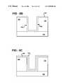
- FIG. 10Ais three-dimensional view of a memory element of the present invention comprising a cup-shaped surface with an open end adjacent to the memory material;
- FIG. 10Bis cross-sectional view of a memory element of the present invention comprising a cup-shaped surface with an open end adjacent to the memory material;
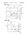
- FIG. 11Ais a three-dimensional view of a memory element having a contact which is a contact layer adjacent to the memory material.
- FIG. 11Bis a cross-sectional view of a memory element having a contact which is a contact layer adjacent to the memory material.
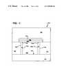
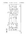
- FIG. 1is a cross-sectional view of a memory device 100 of the present invention formed on a semiconductor substrate 102 .
- the memory device 100comprises two independent single-cell memory elements.
- the first single-cell memory elementcomprises a first contact 130 A, memory material layer 250 , and second contact 270 .
- the second single-cell memory elementcomprises first contact 130 B, memory material layer 250 , and second contact 270 .
- two memory elementsmay share a single continous volume of phase change memory material.
- the insulative layer 260provides for electrical isolation between the memory material 250 and the horizontally disposed section of the second contact 270 .
- the insulative layer 260also provides a thermal blanket keeping heat energy within the memory material layer 250 .
- the dielectric region 140electrically isolates the first contact 130 A from the first contact 130 B.
- the first contacts 130 A,B and the second contact 270supply an electrical signal to the memory material.
- Upper dielectric region 180is deposited on top of the memory device 100 .
- the upper dielectric layer 180comprises borophosphosilicate glass (BPSG).
- the first contacts 130 A,Bare conductive sidewall spacers (also referred to herein as “conductive spacers”) formed along the sidewall surfaces 128 S of the dielectric regions 128 .
- conductive spacersalso referred to herein as “conductive spacers”
- the volume of memory materialis a planar memory material layer 250 that is substantially horizontally disposed and positioned above the conductive sidewall spacers 130 A,B so that the bottom surface of the memory layer 250 is adjacent to the top of each of the conductive spacers 130 A,B (where “top” is defined relative to the substrate).
- the memory materialis adjacent to an edge of the conductive sidewall spacer.
- the memory layer 250is adjacent to the edges 132 A,B of the conductive spacers 130 A,B, respectively.
- the edges 132 A,Bare lateral cross-sections of the conductive spacers 130 A,B.
- the area of contact between the memory material and the conductive spacers 130 A,Bis the area of contact between the memory material and the edges 132 A,B. Hence, the only electrical coupling between the memory material and the conductive spacers 130 A,B is through all or a portion of the edges 132 A,B. The remainder of the conductive spacers 130 A,B is electrically isolated from the memory material by dielectric regions 128 and 140 .
- the memory elements of the present inventionmay be electrically coupled to isolation/selections devices and to addressing lines in order to form a memory array.
- the isolation/addressing devicespermit each discrete memory cell to be read and written to without interfering with information stored in adjacent or remote memory cells of the array.
- the present inventionis not limited to the use of any specific type of isolation/addressing device.
- isolation/addressing devicesinclude field-effect transistors, bipolar junction transistors, and diodes.
- Examples of field-effect transistorsinclude JFET and MOSFET.
- Examples of MOSFETinclude NMOS transistors and PMOS transistors. Furthermore NMOS and PMOS may even be formed on the same chip for CMOS technologies.
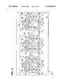
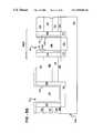
- FIG. 2is a cross-sectional view of a memory array structure 200 comprising the memory device 100 described above.
- Each of the memory elements of memory device 100is electrically coupled to a selection/isolation device which is in the form of an NMOS transistor.
- the memory array 200may be formed on a single crystal silicon semiconductor wafer 102 which is p-doped and which forms a p-substrate for the deposition of the remaining elements of the configuration illustrated.
- the NMOS transistorsinclude n-doped source regions 110 , n-doped drain regions 112 , and gate regions 118 .
- the source regions 110 and the drain regions 112may comprise more than one portion of n-doped material, namely a lightly doped n ⁇ portion and a more heavily doped n+ portion.
- the n-doped source regions 110 and drain regions 112are separated by channel regions 114 .
- the gate regions 118formed above the channel regions 114 , control the flow of current from the source regions to the drain regions through the channel regions 114 .
- the gate regions 118preferably comprise a layer of polysilicon. Separating the gate regions 118 from the channel regions 114 are dielectric regions 116 which are preferably layers of silicon dioxide.
- channel lengthis the distance between source and drain regions.
- the channel lengthis oriented parallel to the current flow between the two regions, which is parallel to the plane of the illustration of FIG. 2 .
- the “length” of the memory arrayis the dimension of the array parallel to the channel length.
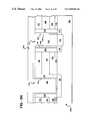
- FIG. 3is a cross-sectional view of the memory array structure 200 parallel to the channel width. The view shows a plurality of conductive sidewall spacers which are electrically isolated from each other by dielectric regions 184 , along the width of the memory array.
- channel stop regions 113are formed in the n-doped drain regions 112 creating two neighboring, electrically isolated drain regions 112 for separate NMOS transistors.
- the channel stop regions 113have a conductivity type opposite that of the source and drain regions 110 , 112 .
- the channel stop regions 113comprises p-doped silicon.
- the channel stop regions 113may be formed by the implantation of boron ions using well known ion implantation techniques.
- metal regions 120are Formed above the gate regions 118 are metal regions 120 which preferably comprise a layer of tungsten silicide. Metal regions 120 are used to deliver the electrical signal to the gate regions 118 .
- the metal regions 120extend across the width of the memory array structure (parallel to the channel width), perpendicular to the plane of the illustration of FIG. 2 and form a first set of addressing lines, in this case the x set of an x-y grid for addressing the individual memory elements of the array.
- the dielectric regions 122Formed above the metal regions 120 are the dielectric regions 122 preferably comprising a layer of silicon dioxide.
- the dielectric regions 122electrically insulates the metal regions 120 from neighboring regions of the memory device.
- the stack of layers 114 , 116 , 118 , 120are collectively referred to as the gate stacks 124 .
- Dielectric regions 128are formed on the sidewall surfaces of the gate stacks 124 .
- Metal lines 190are formed on top of the upper insulation regions 180 and extend across the length of the memory array structure (parallel to the channel length), parallel to the plane of FIG. 2 .
- Metal lines 190form a second set of addressing lines, in this case the y set of an x-y grid for addressing the individual memory cells of the array.
- the metal lines 190may be formed from a conductive material such as aluminum or copper.
- Tungsten plugs 144electrically connect the metal lines 190 to the drain regions 110 . It is noted that in the particular embodiment shown in FIG. 2 , each of the tungsten plugs 144 is shared by two NMOS transistors.
- a layer of titanium silicide(not shown) may be formed on the surface of the silicon substrate to improve the conductivity between the substrate 102 and the conductive sidewall spacers 130 a,b as well as between the substrate 102 and the conductive plugs 144 .
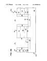
- isolation/addressing devicewhich serves as an isolation/addressing device for that memory element thereby enabling that cell to be read and written without interfering with information stored in other adjacent or remote memory elements of the array.
- the isolation/addressing deviceis an NMOS device.
- the electrical coupling between the memory material 250 , first contact 130 A,B, second contact 270 , isolation transistor, and addressing linesmay be summarized as follows.
- the NMOS transistor gate (gate region 118 )is electrically connected to an x-addressing line (metal region 120 )
- the transistor drain (drain region 110 )is electrically connected to a y-addressing line (metal line 190 via conductive plug 144 )
- the transistor source (source region 112 )is electrically connected to one terminal of a memory element (first contact 130 A or 130 B).
- the other terminal of the memory device (second contact 270 )is electrically coupled to a voltage source Va (not shown in FIG. 2 ).
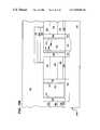
- FIG. 4is a schematic diagram of the memory array illustrating the electrical connections between each of the memory elements 110 , a corresponding field-effect-transistor (FET) 115 , and the X,Y addresssing lines 120 , 190 that are used to selectively set and read the individual memory elements.
- the FETis preferably a MOSFET, and more preferably an NMOS transistor. Alternately, the MOSFET may be a PMOS. It is noted that the x and y addressing lines are connected to external circuitry in a manner well known to those skilled in the art.
- the gate of the FET transistoris connected to one of the addressing lines.
- the drainis connected to a second addressing line.
- source of the transistormay instead be connected to the second addressing line.
- FIGS. 5A–5OAn embodiment of a method for fabricating the memory array structure 200 from FIG. 2 is shown in FIGS. 5A–5O .
- an NMOS transistor array 500 Ais provided.
- FIG. 5Ashows a cross-sectional view of a portion of an NMOS transistor array comprising n-doped regions 110 and 112 formed in a p-doped substrate 102 .
- the transistor arrayincludes gate stacks 104 which include dielectric region 116 , gate region 118 , metal region 120 and dielectric region 122 .
- Dielectric regions 124are formed as insulative sidewall spacers on the sidewall surfaces of the gate stacks 104 .
- Dielectric regions 124are preferably formed from a dielectric material such as TEOS oxide, silicon dioxide, or silicon nitride.
- the thickness of the dielectric regions 124is preferably between about 400 angstroms and 1000 angstroms, more preferably between about about 600 and 800 angstroms, and most preferably about 700 angstroms.
- the spaces between the dielectric regions 124form trenches 170 , 172 extending perpendicular to the plane of the illustration.
- a layer of titanium silicide(not shown) may be formed above the n-doped regions 110 , 112 .
- a dielectric layer 126is conformally deposited onto the NMOS transistor structure 500 A to form the resulting structure 500 B that is shown in FIG. 5B .
- the thickness of the dielectric layer 126is preferably between 100 and 500 angstroms, more preferably between about 150 and about 350 angstoms, and most preferably about 300 angstroms.
- the dielectric layer 126is preferably formed from a material such as TEOS oxide, silicon dioxide, or silicon nitride.
- the structure 500 Bis appropriately masked (i.e., deposition and patterning of photoresist) and anisotropically etched to remove the dielectric layer 126 from the horizontally disposed bottom surface 173 of trench 172 .
- the maskis patterned so that the anisotropic etch removes the dielectric layer 126 from the bottom surface 173 of trench 172 but does not remove the dielectric layer 171 from the bottom surface of trench 170 .
- a cross-sectional view of the mask and the result of the anisotropic etchis shown as structure 500 C in FIG. 5C .
- the first contacts 130 A,B of FIG. 5are formed.
- the first contacts 130 A,Bare formed as conductive sidewall spacers along the sidewall surfaces 126 S of dielectric layers 126 within trench 172 .
- a contact layer 133is conformally deposited onto structure 500 C.
- the resulting structure 500 Dis shown in FIG. 5D .
- the layer 133is desposited on the sidewall surfaces 126 S and bottom surfaces both trenches 170 and 172 (of course, the bottom surface of trench 170 is already covered by a dielectric layer 126 ).
- the conformal depositionmay be done using chemical vapor deposition (CVD) techniques. Other possible deposition methods may be used as long as the sidewall surfaces are covered by the contact layer 133 .
- CVDchemical vapor deposition
- the structure 500 Dis anisotropically etched to form the contuctive sidewall spacers 130 A,B shown in FIG. 5E (structure 500 E)
- the anisotropic etchremoves the contact layer 133 from the horizontally disposed surfaces.
- the contact layers 133 remaining on the sidewall surfaces 126 S of trench 172are referred to herein as “sidewall layers”. These sidewall layers form the conductive sidewall spacers 130 A,B.
- Conductive sidewall spacers 130 A,Bare the first electrical contacts for the memory device 100 .
- the contact layer 133 remaining on the sidewall surfaces 126 S within trench 170will be removed by a later step in the fabrication process.
- the conductive sidewall spacers 130 A,Bwill have a lateral thickness substantially equal to the selected thickness of the contact layer 133 .
- the contact layer 133is deposited so that the resulting conductive sidewall contacts 130 A,B have substantially uniform thickness between about 50 and about 1000 Angstroms, and more preferably between about 100 and about 500 Angstroms.
- the contact layer 133 and the resulting conductive sidewall contacts 130 A,Bmay be formed from any electrically conductive material.
- materialsinclude titanium nitride, titanium aluminum nitride, titantium carbonitride, titanium silicon nitride.
- materialsinclude molydenum, carbon, tungsten, and titanium-tungsten.
- the anisotropic etch which removes the contact layer 133 from the bottom surface of trench 172also removes the titanium silicide layer from the bottom of the same trench 172 thereby electrically isolating conductive sidewall spacer 130 A from conductive sidewall spacer 130 B.
- the titanium silicide at the bottom surface of trench 170is not removed because it is protected from the anisotropic etch by the dielectric layer 126 .
- channel stop region 113is formed in the n-doped drain region 112 creating two neighboring, electrically isolated drain regions 112 .
- the channel stop region 113has a conductivity type opposite that of the source and drain regions 110 , 112 .
- the channel stop region 113comprises p-doped silicon.
- the channel stop region 113may be formed by the implantation of boron ions using well known ion implantation techniques.
- the resulting structure 500 Fis shown in FIG. 5F .
- the structure 500 Fis appropriately masked (via photoresist deposition and patterning) and isotropically etched to remove the remaining contact layer 133 from the sidewalls surfaces 126 s in trench 170 .
- the conductive sidewall spacers 130 A,B in trench 172are protected from the isotropic etch by the photoresist mask. The etch is selected so that it does not remove the dielectric layer 126 from trench 170 .
- a cross-sectional view of the mask and the resulting structure after the isotropic etchis shown as structure 500 G in FIG. 5G .
- FIG. 3is a cross-section view of the memory array through a conductive sidewall spacer ( 130 A or 130 B) and parallel to the width of the memory array.
- FIG. 3shows how the mask and etch may be used to create a plurality of conductive sidewall spacers, having width W, spaced along the width of the memory array.
- the thickness of the layer 140is selected to fill trench 170 and trench 172 .
- the thickness of the layer 140is preferably between about 500 and about 5000 angstroms, and it is more preferably between about 1000 and about 3000 angstroms. Examples of materials which may be used for the dielectric layer 140 include TEOS oxide, silicon dioxide and silicon nitride.
- the structure 500 His chemically mechanically polished (CMP).
- CMPchemically mechanically polished
- the CMP processcontinues at least until the conductive sidewall spacers 130 A,B are exposed.
- the resulting structure, after the CMP is complete,is shown as structure 500 I in FIG. 5I .
- phase change memory material 250is deposited onto structure 500 I.
- a layer of insulation material 260is deposited on top of the phase change memory material 250
- a layer of a conductive material 270is deposited on top of the insulation material 260 .
- the resulting structure 500 Jis shown in FIG. 5J .
- the structure 500 jis masked and layers 250 , 260 , 270 are anisotropically etched to form structure 500 k shown in FIG. 5K .
- Layers 250 , 260 , 270are anisotropically etched away from the top of the trench 170 .
- a layer 280 of conductive materialis conformally deposited on top of structure 500 K to form structure 500 L in FIG. 2L .
- the conductive layer 280is anisotropically etched so that only the sidewall layers 270 B deposited along the sidewall surfaces of layers 250 , 260 , 270 remain.
- the resulting structure 500 Mis shown in FIG. 5M .
- Conductive layers 270 A and 270 Bcollectively form a second contact 290 for the memory device. In the embodiment shown, only a portion of the side layers 280 of the second contact 290 are adjacent to the memory layer 250 .
- the conductive layers 270 A and 270 Bmay all be formed of the same conductive material or they may be formed from different conductive materials.
- Examples of the materials which may be used for conductive layers 270 A and/or 270 Binclude titanium nitride, titanium aluminum nitride, titantium carbonitride, titanium silicon nitride.
- Other examples of materialsinclude molydenum, carbon, tungsten, and titanium-tungsten.
- An upper dielectric layer 180is formed over the semiconductor device structure 500 M to form structure 500 N shown in FIG. 5N .
- the upper dielectric layer 180comprises borophosphosilicate glass (BPSG).
- BPSGborophosphosilicate glass
- the thickness of the upper dielectric layer 180may be between 6,000 and 10,000 angstroms. More preferably the thickness of layer 300 is between 7,000 and 9,000 angstroms, and most preferably about 8,000 angstroms.
- the upper dielectric layer 180is appropriately masked and a selective anisotropic contact etch may be used to form the opening in trench 170 for a conductive plug.
- the selective etchwill etch different dielectric materials at different rates.
- gate stacks 104 and dielectric regions 124are protected during the etch, but the dielectric material 140 is etched away until the silicon substrate 102 (or the titanium silicide layer above the n-doped silicon) is reached.
- the opening in trench 170can be filled with a conductive material, such as tungsten.
- Tungsten plugs 144may be formed by a blanket tungsten deposition and etch-back.
- the conductive lines 190can then be patterned over the tungsten plugs 144 .
- the method of fabrication detailed abovedescribes a way of making a memory array structure using only three masking steps beyond conventional CMOS logic.
- the minimal unit cell area of the memory array structure of the present invention(an embodiment of which is shown in both FIGS. 2 and 3 ) preferably has a cell area which is less then 8F 2 and more preferably less than 6F 2 .
- the method for fabricating the memory array disclosedpreferably requires three or less masking steps masking steps beyond conventional CMOS processing.
- a method for fabricating an electrically operated memory array having a cell area less than 8F 2the method comprising three or less masking steps in addition to the number of masking steps used for a CMOS process flow. Also disclosed is a method for fabricating an electrically operated memory array having a cell area less than 6F 2 , the method comprising three or less masking steps in addition to the number of masking steps used for a CMOS process flow.
- the phase change memory element of the present inventionis a non-charge-measurement memory device so that the fabrication method described above discloses a method for fabricating a non-change-measurement, electrically opererated memory array comprising three or less masking steps in addition to the number of masking steps used for a CMOS process flow.
- phase change memory element of the present inventionis also non-charge-storage memory device so that the fabrication method described above discloses a method for fabricating a non-charge-storage, electrically operated memory array comprising three or less masking steps in addition to the number of masking steps used for a CMOS process flow.
- the following tableis a comparison of the phase-change memory array of the present invention compared to DRAM, SRAM, FLASH memory, and Ferroelectric memory with respective to (1) cell area, and (2) the number masking steps needed in addition to the number of masking steps used for a CMOS process flow.
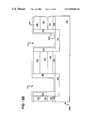
- the conductive sidewall spacers 130 A,Bmay be modified by narrowing their width (i.e. their dimension parallel to the channel width) adjacent to the memory material.
- FIG. 6shows a cross-sectional view of the conductive sidewall spacer 130 A,B parallel to the channel width.
- the top surfaces of the conductive spacers 130 A,Bhave been appropriately etched to form narrowed, protruding columns 188 adjacent to the memory material (the columns protrude toward the memory layer 250 ).
- the height of the columns as well as the extent of taperingmay be controlled so as to adjust both the width as well as the cross-sectional area of the conductive sidewall spacer adjacent to the memory material.
- the width and cross-sectional areacan be made to be the smallest adjacent to the memory material.
- the narrowed conductive sidewall spacers 130 A,B of FIG. 6may be made by forming oxide spacers over the conductive spacers 130 A,B of FIG. 3 at those positions where a narrowed width is desired.
- the oxide spacersmay be used as masks for anisotropic or isotropic etches which will etch the exposed sections of the conductive spacer but leave those sections of the conductive spacer underlying the mask.
- the shape of the conductive sidewall spacers as well as their orientation with respect to the memory materialalso decreases the amount of heat energy transferred back into the conductive spacer from the memory material back.
- each of the first contacts 130 A,Bis a conductive sidewall spacer formed from a single layer of conductive material.
- the conductive spacermay be formed by the conformal deposition of a single contact layer onto a sidewall surface followed by an anisotropic etch of the contact layer.
- the conductive sidewall spacersmay be formed as a multi-layered conductive spacer from more than one contact layer.
- the conductive sidewall spacers of the present inventionmay be formed from one or more, two or more, three or more contact layers.
- the memory device 300 shown in FIG. 7is an alternate embodiment of the memory device of the present invention wherein each of the first contacts 130 a,b is a conductive sidewall spacer formed from two contact layers. Like the memory device 100 shown in FIG. 1 , the memory device 300 comprises two memory elements.
- FIGS. 8A–8Gshows how the memory device 300 may be fabricated.
- a substrate 102 and dielectric layer 128forming a trench 172 with sidewall surfaces 128 S and bottom surface 106 .
- the trench 172extends perpendicular to the plane of the illustration.
- a first contact layer 332is conformally deposited onto the top surface of layer 128 and into the trench 172 , covering trench sidewall surfaces 128 S and trench bottom surface 106 .
- a second contact layer 334is then conformally deposited onto the first contact layer 332 .
- both the first and second contact layers 332 , 334are anisotropically etched to remove the horizontally disposed portions of these layers.
- first sidewall layers 342The remaining portions of the first contact layer 332 , after the anisotropic etch, are referred to as the first sidewall layers 342 .
- the remaining portions of the second contact layer 334are referred to as the second sidewall layers 344 .
- the first sidewall layer 342 and the second sidewall layer 344form a dual-layered conductive sidewall spacer. It is noted that the first sidewall layer, while substantially formed on the sidewall surface 128 S has a small “foot” region 343 formed on the bottom surface 106 .
- the lateral thickness of the first sidewall layer 342is substantially equal to the selected thickness of the first contact layer 342 .
- the thickness of the first contact layer 332is selected so that first sidewall layer 342 may have a substantially uniform thickness between about 50 and about 1000 Angstroms, and preferably it will have a substantially uniform thickness between about 100 and about 500 Angstroms.
- the laterial thickness of the second sidewall layer 344is substantially equal to the selected thickness of the second contact layer 334 .
- the thickness of the second contact layer 334is selected so that the second sidewall layer 344 may have a substantially uniform thickness between about 50 and about 1000 Angstroms, and preferably it will have a substantially uniform thickness between about 100 and about 500 Angstroms.
- a dielectric layer 350is deposited onto the structure, filling the trench 172 .
- the top of the structureis then chemically mechanically polished (CMP) so as to planarize the top surface and expose the top edges 346 , 348 of the first and second sidewall layers 342 and 344 , respectively.
- CMPchemically mechanically polished
- the edges 346 , 348are cross-sections of the thicknesses of the first and second sidewall layers.
- the edges 346 , 348are lateral cross-sections of the first and second sidewall layers 342 , 344 , respectively.
- the first sidewall layers 342are selectively etched so that the top edges 346 are etched below the top edges 348 of the adjacent second sidewall layer creating indentations in the first sidewall layers 342 .
- a dielectric layer 360may then be deposited over the structure so as to fill these indentations.
- the dielectric layer 360may be formed of TEOS oxide, silicon dioxide, or silicon nitride.
- the structureis again chemically mechanically polished to planarize the top surface and ensure that the top edges 348 of the second sidewall layer 344 is exposed.
- Memory layer 250 , insulation layer 260 , and conductive layer 270are deposited as described above to form the structure shown in FIG. 7 .
- top edge 348 of the second sidewall layer 344is adjacent to the memory material and makes contact with the memory material.
- the top edge 346 of the first sidewall layer 342is remote to the memory material and does not make contact with the memory material.
- the top edge 346 of the first contact layer 342is physically separated from the memory material by the dielectric material 360 .
- the area of contact between the dual-layered conductive sidewall spacers 330 A,B and the memory material 250is the area of contact between the top edge 348 of the second sidewall layer 344 and the memory material 250 .
- the first sidewall layers 342are not contiguous with the memory material 250 and are only indirectly electrically coupled to the memory material 250 through the second sidewall layers 344 .
- the materials for the first and second sidewall layers 342 , 344are preferably selected so that the electrical resistivity of the first sidewall layer 342 is less than the electrical resistivity of the second sidewall layer 344 .
- first sidewall layer 342examples include titanium tungsten, tungsten silicide, tungsten, molydenum, and N+ doped polysilicon, and titanium nitride.
- the first sidewall layer 342may have a thickness between about 50 angstoms and 300 angstroms, and preferably between about 100 angstroms and 200 angstroms.
- the second sidewall layer 344preferably has a resisitivity which is greater than the resistivity of the first sidewall layer.
- materials which may be used for the second sidewall layerinclude titanium nitride, titanium carbonitride, titantium aluminum nitride, titanium siliconitride, carbon, N ⁇ doped polysilicon, and forms of titanium nitride.
- the second sidewall layer 132may have a thickness between about 50 angstroms and 300 angstroms, and preferably between about 100 angstroms and 200 angstroms.
- the dual-layered conductive sidewall spacers 330 A,Bmay be thought of as having a first segment L 1 extending from substrate 102 to edge 346 of first sidewall layer 342 , and a second segment L 2 extending from edge 346 to edge 348 of second sidewall layer 344 (adjacent to the memory material).
- first sidewall layer 342electrically shunts (provides a parallel or alternative electrical path for) the second sidewall layer 344 .
- the first and second sidewall layersare electrically in parallel so current can pass through either layer. Since the resistivity of the first sidewall layer is less than the resistivity of the second sidewall layer, most of the electrical current will pass through the first sidewall layer. Segment L 1 thus provides a low resistance current path.
- segment L 2For segment L 2 , all of the electrical current must pass through the more resistive second sidewall layer. Segment L 2 thus provides a high resistance current path. (It is noted that the resistivity of segment L 2 is higher than that of L 1 when the resistivities of the two sidewall layers are not the same.) Since the resistance of the segment L 2 is greater than that of L 1 most of the Joule heating within the dual layered conductive sidewall spacer will occur in section L 2 adjacent to the memory material. This provides for more efficient heating of the memory material.
- the first electrical contacts of each of the memory elementsare conductive sidewall spacers formed by depositing one or more contact layers onto the sidewall surfaces of a trench.
- the conductive sidewall spacersmay be formed by conformally depositing one or more contact layers onto the sidewall surface or surfaces of a via hole.
- the via holemay be round, square, rectangular or irregularly shaped.
- the conductive sidewall spacersmay also be formed by conformally depositing one or more contact layers onto the sidewall surfaces of a pillar or mesa.
- FIG. 9shows a three-dimensional view of a memory structure comprising a first contact 400 , a layer of memory material 250 , and a second contact 410 .
- the first contact 400is a conductive sidewall spacer formed by conformally depositing a contact layer into a round via and then anisotropically etching the contact layer to remove the horizontally disposed surfaces. The remaining portion on the sidewall surface of the via is the tubular shaped conductive sidewall spacer 400 .
- the remaining space in the viais filled with a dielectric material and the structure is then chemically mechanically polished to expose the conductive sidewall spacer.
- a layer of memory materialis deposited onto the top of the structure so that the bottom surface of the memory material makes contact with the annular top edge of the conductive sidewall spacer.
- a layer of conductive materialis deposited on top of the memory material to form a second contact.
- the conductive sidewall spacer 400has a annular top edge 402
- the thickness of the conductive sidewall spacer 400 , and the thickness of the annular top edge 402is substantially equal to the thickness of the conformally deposited contact layer.
- the edge 402is a lateral cross-section of the conductive spacer 400 .
- the area of contact between the conductive spacer 400 and the memory material 250is the area of contact between the memory layer 250 and the annular edge 402 . If the entire edge 402 makes contact with the memory layer, then the area of contact is an annular ring. The area of contact is proportional to the thickness of the edge which is substantially equal to the thickness of the deposited contact layer. Hence, the area of contact can thus be reduced by controlling the deposition process of the contact layer and the size of the effective electrode area of the memory device shown in FIG. 9 may be reduced beyond that permitted by the resolution of photolithography.
- the first contact 400 shown in FIG. 9is formed as the conductive sidewall spacer 400 having a tubular shape with two open ends.
- the contactmay be formed as a cup-shaped shell 450 having the three-dimensional view shown in FIG. 10 a and the cross-sectional view shown in FIG. 10 b .
- the contact 450has edge 460 which is adjacent to the memory material.
- the area of contact between the contact 450 and the memory material 250is the area of contact between the edge 460 and the memory material 250 .
- the cup-like shell 450may be formed by depositing a contact layer into a via, filling the remainder of the via with a dielectric, and chemically mechanically polishing the surface to planarize the surface and expose the top edge 460 of the contact 450 .
- the layers 250 and 410may then be deposited.
- the area of contact between the contact 450 and the memory materialis the region of contact between the edge 460 and the memory material. If the entire edge makes contact with the memory material then the area of contact is in the form of an annular ring.
- an electrically programmable memory elementcomprising a volume of phase change memory material, a first electrical contact, and second electrical contact, where the first contact comprises a contact layer having an edge adjacent to the volume of phase change memory material.
- the contact layeris not restricted to any specific orientation or conformation.
- the contact layermay be substantially vertically disposed.
- the contact layermay be substantially vertically disposed, for example, by forming the first contact as a conductive sidewall spacer on a substantially vertically disposed sidewall surface.
- the contact layermay be substantially horizontally disposed.
- the contact layermay be substantially horizontally disposed by depositing the contact layer onto a substantially horizontally disposed subtrate.
- FIG. 11Ashows a three-dimensional view of an alternate embodiment of a memory element of the present invention formed on a single crystal silicon semiconductor substrate wafer 102 .
- the memory element 600comprises the volume of memory material 250 , a first electrical contact 610 which is electrically coupled to the memory material 250 , and a second electrical contact which is electrically coupled to the memory material and which is spacedly disposed from the first contact 610 .
- FIG. 11Bis a cross-sectional view of the same memory device 600 .
- the first contactis a contact layer 610 which is substantially horizontally disposed onto the substrate 102 .
- the contact layerhas an edge 612 which is adjacent to the volume of memory material 250 .
- the area of contact between the memory material 250 and the contact layer 610is the area of contact between the memory material 250 and edge 612 . (As shown, in this embodiment the edge, is a cross-sectional slice parallel to the thickness).
- the area of contact between the contact layer 610 and the memory material 250is proportional to the thickness of the contact layer 610 . It is noted that electrical coupling between the memory material and the contact layer 610 is by way of all or a portion of the edge 612 .
- the remainder of the volume of memory material 250is electrically isolated from the first contact 610 by the dielectric material 628 .
- the edge 612encircles a cross-sectional slice of the volume of memory material 250 .
- “encircles”means that the edge 612 passes completely around a cross-sectional slice of the volume of memory material 250 .
- the memory elementmay be structured so that the edge only partially encircles a cross-sectional slice of the volume of memory material 250 .
- the cross-sectional sliceis substantially parallel to the plane of the substrate 102 , however, other orientations are also possible.
- the second contactmay be as a layer of conductive material and is preferably formed as a thin-film layer.
- the second contact 620is a conductive layer 620 that is deposited on top of the memory material 250 so that the bottom surface of the conductive layer 620 is adjacent to the top surface of memory material 250 .
- an electrically programmable, single-cell memory elementcomprising a volume of phase-change memory material; and a first and a second contact for supplying an electrical signal to the memory material where at least one of the contacts is adapted to maximize the current density adjacent to the memory material and to minimize the thermal energy flowing from the memory material to the contact.
- phase-change memory material used in the memory elements and memory arrays of the present inventionmay be any phase-change memory material known in the art. Specific materials are described in U.S. Pat. Nos. 5,166,758, 5,296,716, 5,414,271, 5,359,205, 5,341,328, 5,536,947, 5,534,712, 5,687,112, and 5,825,046 the disclosures of which are all incorporated by reference herein.
- the phase change materialsare preferably directly overwritable so that they can be set directly to one of a plurality of resistance values without the need to be set to a specific starting or erased resistance value, regardless of the previous resistance value of the material in response to a selected electrical input signal.
- the phase change materialspreferably have a large dynamic range which provide for gray scale storage of multiple bits of binary information in a single cell by mimicking the binary encoded information in analog form and thereby storing multiple bits of binary encoded information as a single resistance value in a single cell.
- phase change materialsmay have a dynamic range of electrical resistance values with the ability to be set directly to one of a plurality of resistance values within the dynamic range without the need to be set to a specific starting or erased resistance value, regardless of the previous resistance value of the material in response to a selected electrical input signal.
- the volume of memory material defining a single-cell memory elementmay have a dynamic range of resistance which provides for two distinct detectable levels of electrical resistance values, thereby providing for single-bit data storage capabilities.
- the volume of memory material defining a single-cell memory elementmay have at least three distinct detectable levels of electrical resistance values and thus be capable of storing more than one bit of binary information, thereby providing the memory element with multibit storage capabilities.
- the volume of memory material defining a single-cell memory elementmay have at least four distinct detectable levels of electrical resistance values so that the dynamic range and the multibit capabilities provide storage for at least two bits of binary information in a single-cell memory element.
- the dynamic range of resistanceprovides for at least sixteen distinct detectable levels of electrical resistance values so that the dynamic range and the multibit capabilities provide storage for at least four bits of binary information in a single-cell memory element.
- the phase change memory materialsmay be formed from a plurality of atomic elements, each of which is present throughout the entire volume of memory material.
- the memory materialincludes at least one chalcogen element.
- the chalcogen elementsare selected from the group consisting of Te, Se, and mixtures or alloys thereof. More preferably, the memory material includes a mixture of Te and Se.
- the memory materialmay further include at least one element selected from the group consisting of Ge, Sb, Bi, Pb, Sn, As, S, Si, P, O, and mixtures or alloys thereof.
- the memory materialmay include at least one transition metal element.
- transition metalas used herein includes elements 21 to 30 , 39 to 48 , 57 and 72 to 80 .
- the one or more transition metal elementsare selected from the group consisting of Cr, Fe, Ni, Nb, Pd, Pt and mixtures or alloys thereof.
- compositions in the highly resistive state of the class of TeGeSb materials which meet the criteria of the present inventionare generally characterized by substantially reduced concentrations of Te relative to that present in prior art electrically erasable memory materials.
- the average concentration of Te in the as deposited materialswas well below 70%, typically below about 60% and ranged in general from as low as about 23% up to about 58% Te and most preferably about 40% to 58% Te.
- Concentrations of Gewere above about 5% and ranged from a low of about 8% to about 30% average in the material, remaining generally below 50%.
- the remainder of the principal constituent elements in this compositionwas Sb.
- the percentages givenare atomic percentages which total 100% of the atoms of the constituent elements.
- this compositionmay be characterized as Te a Ge b Sb 100-(a+b) .
- the memory material of the present inventionincludes at least one chalcogen and may include at least one transition metal element.
- the memory materials which include transition metalsare elementally modified forms of the memory materials in the Te—Ge—Sb ternary system. That is, the elementally modified memory materials constitute modified forms of the Te—Ge—Sb memory alloys. This elemental modification is achieved by the incorporation of transition metals into the basic Te—Ge—Sb ternary system, with or without an additional chalcogen element, such as Se. Generally the elementally modified memory materials fall into two categories.
- the first categoryis a phase-change memory material which includes Te, Ge, Sb and a transition metal, in the ratio (Te a Ge b Sb 100-(a+b) ) c TM 100-c where the subscripts are in atomic percentages which total 100% of the constituent elements, wherein TM is one or more transition metals, a and b are as set forth herein above for the basic Te—Ge—Sb ternary system and c is between about 90% and about 99.99%.
- the transition metalpreferably include Cr, Fe, Ni, Nb, Pd, Pt and mixtures or alloys thereof.
- the second categoryis a phase-change memory material which includes Te, Ge, Sb, Se and a transition metal, in the ratio (Te a Ge b Sb 100-(a+b) ) c TM d Se 100-(c+d) where the subscripts are in atomic percentages which total 100% of the constituent elements, TM is one or more transition metals, a and b are as set forth hereinabove for the basic Te—Ge—Sb ternary system, c is between about 90% and 99.5% and d is between about 0.01% and 10%.
- the transition metalcan preferably include Cr, Fe, Ni, Pd, Pt, Nb, and mixtures or alloys thereof.
- the memory elements of the instant patent applicationpossess substantially non-volatile set resistance values. However, if the resistance value does, under some circumstances, drift from its original set value, “compositional modification”, described hereinafter, may be used to compensate for this drift.
- the term “non-volatile”will refer to the condition in which the set resistance value remains substantially constant for archival time periods.
- softwareincluding the feedback system discussed hereinafter
- drift of the resistance value of the memory elementscan, if left unimpeded, hinder gray scale storage of information, it is desirable to minimize drift.
- compositional modificationis defined herein to include any means of compositionally modifying the volume of memory material to yield substantially stable values of resistance, including the addition of band gap widening elements to increase the inherent resistance of the material.
- One example of compositional modificationis to include graded compositional inhomogeneities with respect to thickness.
- the volume of memory materialmay be graded from a first Te—Ge—Sb alloy to a second Te—Ge—Sb alloy of differing composition.
- the compositional gradingmay take any form which reduces set resistance value drift and need not be limited to a first and second alloy of the same alloy system. Also, the grading can be accomplished with more than two alloys.
- the gradingcan be uniform and continuous or it can also be non-uniform or non-continuous.
- a specific example of compositional grading which results in reduced resistance value driftincludes a uniform and continuous grading of Ge 14 Sb 29 Te 57 at one surface to Ge 22 Sb 22 Te 56 at the opposite surface.
- the volume of memory materialmay be formed of a plurality of discrete, relatively thin layers of differing composition.
- the volume of memory materialmay include one or more pairs of layers, each one of which is formed of a different Te—Ge—Sb alloy.
- Te—Ge—Sb alloyany combination of layers which results in substantially reduced resistance value drift can be employed.
- the layersmay be of similar thickness or they may be of differing thickness. Any number of layers may be used and multiple layers of the same alloy may be present in the volume of memory material, either contiguous or remote from one another. Also, layers of any number of differing alloy composition may be used.
- a specific example of compositional layeringis a volume of memory material which includes alternating layer pairs of Ge 14 Sb 29 Te 57 and Ge 22 Sb 22 Te 56 .
- compositional inhomogeneity to reduce resistance driftis accomplished by combining compositional grading and compositional layering. More particularly, the aforementioned compositional grading may be combined with any of the above described compositional layering to form a stable volume of memory material.
- Exemplary volumes of memory material which employ this combinationare: (1) a volume of memory material which includes a discrete layer of Ge 22 Sb 22 Te 56 followed by a graded composition of Ge 14 Sb 29 Te 57 and Ge 22 Sb 22 Te 56 and (2) a volume of memory material which includes a discrete layer of Ge 14 Sb 29 Te 57 and a graded composition of Ge 14 Sb 29 Te 57 and Ge 22 Sb 22 Te 56 .
Landscapes
- Engineering & Computer Science (AREA)
- Computer Hardware Design (AREA)
- Manufacturing & Machinery (AREA)
- Chemical & Material Sciences (AREA)
- Crystallography & Structural Chemistry (AREA)
- Semiconductor Memories (AREA)
Abstract
Description
| TABLE | |||
| (1) Cell Area | (2) Masking Steps | ||
| DRAM | 8F2 | 6–9 | |
| SRAM | |||
| 4T | 40F2 | 5 | |
| 6T | 80F2 | 0 | |
| FLASH | 8F2 | 5 | |
| FERROELECTRIC | 8F2 | 3 | |
| 6F | 2 | 2–4 | |
Claims (33)
Priority Applications (37)
| Application Number | Priority Date | Filing Date | Title |
|---|---|---|---|
| US09/276,273US6969866B1 (en) | 1997-10-01 | 1999-03-25 | Electrically programmable memory element with improved contacts |
| KR10-2001-7012157AKR100441692B1 (en) | 1999-03-25 | 2000-03-22 | Electrically programmable memory element with improved contacts |
| MXPA01009609AMXPA01009609A (en) | 1999-03-25 | 2000-03-22 | ELECTRICALLY PROGRAMMABLE MEMORY ELEMENT WITH IMPROVED CONTACTS. |
| EP00916621AEP1171920B1 (en) | 1999-03-25 | 2000-03-22 | Electrically programmable memory element with improved contacts |
| BR0009308-4ABR0009308A (en) | 1999-03-25 | 2000-03-22 | Memory element |
| CNB008080437ACN1210819C (en) | 1999-03-25 | 2000-03-22 | Electrically programmable memory element with improved contacts |
| DE60032129TDE60032129T2 (en) | 1999-03-25 | 2000-03-22 | ELECTRICALLY PROGRAMMABLE STORAGE ELEMENT WITH IMPROVED CONTACTS |
| AU37699/00AAU3769900A (en) | 1999-03-25 | 2000-03-22 | Electrically programmable memory element with improved contacts |
| CA002367365ACA2367365A1 (en) | 1999-03-25 | 2000-03-22 | Electrically programmable memory element with improved contacts |
| PCT/US2000/007666WO2000057498A1 (en) | 1999-03-25 | 2000-03-22 | Electrically programmable memory element with improved contacts |
| EP06023789AEP1760797A1 (en) | 1999-03-25 | 2000-03-22 | Electrically programmable memory element with improved contacts |
| JP2000607287AJP4558950B2 (en) | 1999-03-25 | 2000-03-22 | Electrically programmable memory device with improved junction |
| TW089105608ATW475262B (en) | 1999-03-25 | 2000-04-21 | Electrically programmable memory element with improved contacts |
| US09/677,957US6617192B1 (en) | 1997-10-01 | 2000-10-03 | Electrically programmable memory element with multi-regioned contact |
| US09/813,267US6943365B2 (en) | 1999-03-25 | 2001-03-20 | Electrically programmable memory element with reduced area of contact and method for making same |
| US09/891,157US6750079B2 (en) | 1999-03-25 | 2001-06-26 | Method for making programmable resistance memory element |
| US09/921,038US6815705B2 (en) | 1999-03-25 | 2001-08-02 | Electrically programmable memory element with raised pore |
| NO20014633ANO20014633D0 (en) | 1999-03-25 | 2001-09-24 | Electrically programmable memory element with improved contacts |
| US10/269,048US20030075778A1 (en) | 1997-10-01 | 2002-10-10 | Programmable resistance memory element and method for making same |
| US10/649,562US6764897B2 (en) | 1997-10-01 | 2003-08-26 | Method of making programmable resistance memory element |
| US10/799,265US7407829B2 (en) | 1997-10-01 | 2004-03-12 | Electrically programmable memory element with improved contacts |
| US10/801,414US6927093B2 (en) | 1999-03-25 | 2004-03-16 | Method for making programmable resistance memory element |
| US10/848,999US7023009B2 (en) | 1997-10-01 | 2004-05-19 | Electrically programmable memory element with improved contacts |
| US10/891,970US7576350B2 (en) | 1997-10-01 | 2004-07-15 | Programmable resistance memory element with multi-regioned contact |
| US10/981,826US7253429B2 (en) | 1999-03-25 | 2004-11-05 | Electrically programmable memory element |
| US11/122,367US20050201136A1 (en) | 1999-03-25 | 2005-05-05 | Electrically programmable memory element with reduced area of contact and method for making same |
| US11/221,627US7092286B2 (en) | 1999-03-25 | 2005-09-08 | Electrically programmable memory element with reduced area of contact |
| US11/287,833US20060110846A1 (en) | 1997-10-01 | 2005-11-28 | Electrically programmable memory element with improved contacts |
| US11/394,433US7473574B2 (en) | 1997-10-01 | 2006-04-01 | Memory element with improved contacts |
| US11/495,927US7902536B2 (en) | 1999-03-25 | 2006-07-28 | Memory device and method of making same |
| US11/503,606US20060274575A1 (en) | 1999-03-25 | 2006-08-14 | Electrically programmable memory element with reduced area of contact |
| US11/602,923US7723715B2 (en) | 1999-03-25 | 2006-11-21 | Memory device and method of making same |
| US12/069,046US7833823B2 (en) | 1997-10-01 | 2008-02-07 | Programmable resistance memory element and method for making same |
| US12/152,330US7952087B2 (en) | 1999-03-25 | 2008-05-14 | Phase change device with offset contact |
| US12/290,353US20090057645A1 (en) | 1997-10-01 | 2008-10-30 | Memory element with improved contacts |
| US12/944,312US8089059B2 (en) | 1997-10-01 | 2010-11-11 | Programmable resistance memory element |
| US13/039,952US8581223B2 (en) | 1999-03-25 | 2011-03-03 | Memory device and method of making same |
Applications Claiming Priority (2)
| Application Number | Priority Date | Filing Date | Title |
|---|---|---|---|
| US94200097A | 1997-10-01 | 1997-10-01 | |
| US09/276,273US6969866B1 (en) | 1997-10-01 | 1999-03-25 | Electrically programmable memory element with improved contacts |
Related Parent Applications (2)
| Application Number | Title | Priority Date | Filing Date |
|---|---|---|---|
| US94200097AContinuation-In-Part | 1997-10-01 | 1997-10-01 | |
| US62031800AContinuation-In-Part | 1997-10-01 | 2000-07-22 |
Related Child Applications (8)
| Application Number | Title | Priority Date | Filing Date |
|---|---|---|---|
| US62031800AContinuation-In-Part | 1997-10-01 | 2000-07-22 | |
| US09/813,267Continuation-In-PartUS6943365B2 (en) | 1999-03-25 | 2001-03-20 | Electrically programmable memory element with reduced area of contact and method for making same |
| US09/891,157Continuation-In-PartUS6750079B2 (en) | 1999-03-25 | 2001-06-26 | Method for making programmable resistance memory element |
| US09/921,038Continuation-In-PartUS6815705B2 (en) | 1999-03-25 | 2001-08-02 | Electrically programmable memory element with raised pore |
| US10/269,048Continuation-In-PartUS20030075778A1 (en) | 1997-10-01 | 2002-10-10 | Programmable resistance memory element and method for making same |
| US10/799,265ContinuationUS7407829B2 (en) | 1997-10-01 | 2004-03-12 | Electrically programmable memory element with improved contacts |
| US10/848,999Continuation-In-PartUS7023009B2 (en) | 1997-10-01 | 2004-05-19 | Electrically programmable memory element with improved contacts |
| US11/287,833ContinuationUS20060110846A1 (en) | 1997-10-01 | 2005-11-28 | Electrically programmable memory element with improved contacts |
Publications (1)
| Publication Number | Publication Date |
|---|---|
| US6969866B1true US6969866B1 (en) | 2005-11-29 |
Family
ID=26957891
Family Applications (3)
| Application Number | Title | Priority Date | Filing Date |
|---|---|---|---|
| US09/276,273Expired - LifetimeUS6969866B1 (en) | 1997-10-01 | 1999-03-25 | Electrically programmable memory element with improved contacts |
| US10/799,265Expired - Fee RelatedUS7407829B2 (en) | 1997-10-01 | 2004-03-12 | Electrically programmable memory element with improved contacts |
| US11/287,833AbandonedUS20060110846A1 (en) | 1997-10-01 | 2005-11-28 | Electrically programmable memory element with improved contacts |
Family Applications After (2)
| Application Number | Title | Priority Date | Filing Date |
|---|---|---|---|
| US10/799,265Expired - Fee RelatedUS7407829B2 (en) | 1997-10-01 | 2004-03-12 | Electrically programmable memory element with improved contacts |
| US11/287,833AbandonedUS20060110846A1 (en) | 1997-10-01 | 2005-11-28 | Electrically programmable memory element with improved contacts |
Country Status (1)
| Country | Link |
|---|---|
| US (3) | US6969866B1 (en) |
Cited By (119)
| Publication number | Priority date | Publication date | Assignee | Title |
|---|---|---|---|---|
| US20030219924A1 (en)* | 2001-12-05 | 2003-11-27 | Stmicroelectronics S.R.L. | Small area contact region, high efficiency phase change memory cell and fabrication method thereof |
| US20040211953A1 (en)* | 2003-01-15 | 2004-10-28 | Stmicroelectronics S.R.L. | Sublithographic contact structure, in particular for a phase change memory cell, and fabrication process thereof |
| US20040234895A1 (en)* | 2003-05-23 | 2004-11-25 | Lee Jung-Hyun | Semiconductor memory device and method of fabricating the same |
| US20050001284A1 (en)* | 2001-12-05 | 2005-01-06 | Stmicroelectronics S.R.L. | Self-aligned process for manufacturing a phase change memory cell and phase change memory cell thereby manufactured |
| US20050031484A1 (en)* | 2003-07-03 | 2005-02-10 | Mitsubishi Materials Corporation | Phase change recording film having high electric resistance and sputtering target for forming phase change recording film |
| US20050045919A1 (en)* | 2003-08-27 | 2005-03-03 | Nec Corporation | Semiconductor device |
| US20050152208A1 (en)* | 2002-02-20 | 2005-07-14 | Stmicroelectronics S.R.L. | Phase change memory cell and manufacturing method thereof using minitrenches |
| US20050191804A1 (en)* | 2004-03-01 | 2005-09-01 | Taiwan Semiconductor Manufacturing Co., Ltd. | Method for forming a reduced active area in a phase change memory structure |
| US20050255665A1 (en)* | 2002-02-20 | 2005-11-17 | Stmicroelectronics S.R.I | Manufacturing method of a contact structure and phase change memory cell with elimination of double contacts |
| US20060001164A1 (en)* | 2004-06-30 | 2006-01-05 | Chang Heon Y | Phase-change random access memory device and method for manufacturing the same |
| US20060049391A1 (en)* | 2002-02-20 | 2006-03-09 | Stmicroelectronics S.R.L. | Sublithographic contact structure, phase change memory cell with optimized heater shape, and manufacturing method thereof |
| US20060286709A1 (en)* | 2005-06-17 | 2006-12-21 | Macronix International Co., Ltd. | Manufacturing methods for thin film fuse phase change ram |
| US20070051936A1 (en)* | 2005-04-08 | 2007-03-08 | Stmicroelectronics S.R.I. | Phase change memory cell with tubular heater and manufacturing method thereof |
| US20070148814A1 (en)* | 2005-12-22 | 2007-06-28 | Stmicroelectronics S.R.L. | Process for manufacturing a phase change memory array in Cu-damascene technology and phase change memory array thereby manufactured |
| US20070258279A1 (en)* | 2004-01-26 | 2007-11-08 | Macronix International Co., Ltd. | Thin film phase-change memory |
| US20070281420A1 (en)* | 2006-05-30 | 2007-12-06 | Macronix International Co., Ltd. | Resistor random access memory cell with reduced active area and reduced contact areas |
| US20070278529A1 (en)* | 2006-05-30 | 2007-12-06 | Macronix International Co., Ltd. | Resistor random access memory cell with l-shaped electrode |
| US20070298535A1 (en)* | 2006-06-27 | 2007-12-27 | Macronix International Co., Ltd. | Memory Cell With Memory Material Insulation and Manufacturing Method |
| US20080089104A1 (en)* | 2006-09-28 | 2008-04-17 | Hiroyasu Tanaka | Semiconductor memory device and method for fabricating semiconductor memory device |
| US20080096341A1 (en)* | 2006-10-24 | 2008-04-24 | Macronix International Co., Ltd. | Method for Manufacturing a Resistor Random Access Memory with Reduced Active Area and Reduced Contact Areas |
| US7385235B2 (en)* | 2002-08-09 | 2008-06-10 | Macronix International Co., Ltd. | Spacer chalcogenide memory device |
| US20080142776A1 (en)* | 2006-12-15 | 2008-06-19 | Harald Seidl | Phase change random access memory device with transistor, and method for fabricating a memory device |
| WO2008088615A3 (en)* | 2006-11-21 | 2008-09-18 | Ovonyx Inc | Memory device and method of making same |
| US20080246014A1 (en)* | 2007-04-03 | 2008-10-09 | Macronix International Co., Ltd. | Memory Structure with Reduced-Size Memory Element Between Memory Material Portions |
| US20080258125A1 (en)* | 2007-04-17 | 2008-10-23 | Micron Technology, Inc. | Resistive memory cell fabrication methods and devices |
| US7459717B2 (en) | 2005-11-28 | 2008-12-02 | Macronix International Co., Ltd. | Phase change memory cell and manufacturing method |
| US20080308784A1 (en)* | 2007-06-18 | 2008-12-18 | Oh Gyu-Hwan | Variable resistance non-volatile memory cells and methods of fabricating same |
| US7473576B2 (en) | 2006-12-06 | 2009-01-06 | Macronix International Co., Ltd. | Method for making a self-converged void and bottom electrode for memory cell |
| US7476587B2 (en) | 2006-12-06 | 2009-01-13 | Macronix International Co., Ltd. | Method for making a self-converged memory material element for memory cell |
| US20090026437A1 (en)* | 2007-07-25 | 2009-01-29 | Yudong Kim | Copper compatible chalcogenide phase change memory with adjustable threshold voltage |
| US20090032794A1 (en)* | 2007-08-01 | 2009-02-05 | Industrial Technology Research Institute | Phase change memory device and fabrication method thereof |
| CN100502084C (en)* | 2006-08-22 | 2009-06-17 | 旺宏电子股份有限公司 | Thin film phase change cell with thermal insulation layer and method of making same |
| US7560337B2 (en)* | 2006-01-09 | 2009-07-14 | Macronix International Co., Ltd. | Programmable resistive RAM and manufacturing method |
| US7569844B2 (en) | 2007-04-17 | 2009-08-04 | Macronix International Co., Ltd. | Memory cell sidewall contacting side electrode |
| US7599217B2 (en) | 2005-11-22 | 2009-10-06 | Macronix International Co., Ltd. | Memory cell device and manufacturing method |
| US7619311B2 (en) | 2007-02-02 | 2009-11-17 | Macronix International Co., Ltd. | Memory cell device with coplanar electrode surface and method |
| CN100573952C (en)* | 2006-05-09 | 2009-12-23 | 旺宏电子股份有限公司 | Bridge resistance random access memory element using single contact structure and method |
| US7639527B2 (en) | 2008-01-07 | 2009-12-29 | Macronix International Co., Ltd. | Phase change memory dynamic resistance test and manufacturing methods |
| US7642123B2 (en) | 2005-11-15 | 2010-01-05 | Macronix International Co., Ltd. | Thermally insulated phase change memory manufacturing method |
| US7642125B2 (en) | 2007-09-14 | 2010-01-05 | Macronix International Co., Ltd. | Phase change memory cell in via array with self-aligned, self-converged bottom electrode and method for manufacturing |
| US7646631B2 (en) | 2007-12-07 | 2010-01-12 | Macronix International Co., Ltd. | Phase change memory cell having interface structures with essentially equal thermal impedances and manufacturing methods |
| US7688619B2 (en) | 2005-11-28 | 2010-03-30 | Macronix International Co., Ltd. | Phase change memory cell and manufacturing method |
| US20100084625A1 (en)* | 2008-10-02 | 2010-04-08 | Guy Wicker | Memory Device |
| US20100091558A1 (en)* | 2008-10-10 | 2010-04-15 | Macronix International Co., Ltd. | Dielectric-Sandwiched Pillar Memory Device |
| US7701750B2 (en) | 2008-05-08 | 2010-04-20 | Macronix International Co., Ltd. | Phase change device having two or more substantial amorphous regions in high resistance state |
| US7719913B2 (en) | 2008-09-12 | 2010-05-18 | Macronix International Co., Ltd. | Sensing circuit for PCRAM applications |
| CN101226951B (en)* | 2007-01-18 | 2010-06-02 | 旺宏电子股份有限公司 | Resistive random access memory |
| US7741636B2 (en) | 2006-01-09 | 2010-06-22 | Macronix International Co., Ltd. | Programmable resistive RAM and manufacturing method |
| US7772581B2 (en) | 2006-09-11 | 2010-08-10 | Macronix International Co., Ltd. | Memory device having wide area phase change element and small electrode contact area |
| US7777215B2 (en) | 2007-07-20 | 2010-08-17 | Macronix International Co., Ltd. | Resistive memory structure with buffer layer |
| US7786460B2 (en) | 2005-11-15 | 2010-08-31 | Macronix International Co., Ltd. | Phase change memory device and manufacturing method |
| US7785920B2 (en) | 2006-07-12 | 2010-08-31 | Macronix International Co., Ltd. | Method for making a pillar-type phase change memory element |
| US7791057B2 (en) | 2008-04-22 | 2010-09-07 | Macronix International Co., Ltd. | Memory cell having a buried phase change region and method for fabricating the same |
| US7825398B2 (en) | 2008-04-07 | 2010-11-02 | Macronix International Co., Ltd. | Memory cell having improved mechanical stability |
| US7855378B2 (en) | 2007-05-02 | 2010-12-21 | Powerchip Semiconductor Crop. | Phase change memory devices and methods for fabricating the same |
| US7863655B2 (en) | 2006-10-24 | 2011-01-04 | Macronix International Co., Ltd. | Phase change memory cells with dual access devices |
| US7869270B2 (en) | 2008-12-29 | 2011-01-11 | Macronix International Co., Ltd. | Set algorithm for phase change memory cell |
| US7867815B2 (en) | 2005-11-16 | 2011-01-11 | Macronix International Co., Ltd. | Spacer electrode small pin phase change RAM and manufacturing method |
| US7879643B2 (en) | 2008-01-18 | 2011-02-01 | Macronix International Co., Ltd. | Memory cell with memory element contacting an inverted T-shaped bottom electrode |
| US7879645B2 (en) | 2008-01-28 | 2011-02-01 | Macronix International Co., Ltd. | Fill-in etching free pore device |
| US7884343B2 (en) | 2007-02-14 | 2011-02-08 | Macronix International Co., Ltd. | Phase change memory cell with filled sidewall memory element and method for fabricating the same |
| US7894254B2 (en) | 2009-07-15 | 2011-02-22 | Macronix International Co., Ltd. | Refresh circuitry for phase change memory |
| US7903447B2 (en) | 2006-12-13 | 2011-03-08 | Macronix International Co., Ltd. | Method, apparatus and computer program product for read before programming process on programmable resistive memory cell |
| US7903457B2 (en) | 2008-08-19 | 2011-03-08 | Macronix International Co., Ltd. | Multiple phase change materials in an integrated circuit for system on a chip application |
| US7910906B2 (en) | 2006-10-04 | 2011-03-22 | Macronix International Co., Ltd. | Memory cell device with circumferentially-extending memory element |
| US7919766B2 (en) | 2007-10-22 | 2011-04-05 | Macronix International Co., Ltd. | Method for making self aligning pillar memory cell device |
| US7923285B2 (en) | 2005-12-27 | 2011-04-12 | Macronix International, Co. Ltd. | Method for forming self-aligned thermal isolation cell for a variable resistance memory array |
| US7932506B2 (en) | 2008-07-22 | 2011-04-26 | Macronix International Co., Ltd. | Fully self-aligned pore-type memory cell having diode access device |
| US7933139B2 (en) | 2009-05-15 | 2011-04-26 | Macronix International Co., Ltd. | One-transistor, one-resistor, one-capacitor phase change memory |
| US7956344B2 (en) | 2007-02-27 | 2011-06-07 | Macronix International Co., Ltd. | Memory cell with memory element contacting ring-shaped upper end of bottom electrode |
| US7968876B2 (en) | 2009-05-22 | 2011-06-28 | Macronix International Co., Ltd. | Phase change memory cell having vertical channel access transistor |
| US7978509B2 (en) | 2007-08-02 | 2011-07-12 | Macronix International Co., Ltd. | Phase change memory with dual word lines and source lines and method of operating same |
| US7993962B2 (en) | 2005-11-15 | 2011-08-09 | Macronix International Co., Ltd. | I-shaped phase change memory cell |
| US20110193048A1 (en)* | 2007-06-18 | 2011-08-11 | Samsung Electronics Co., Ltd. | Non-volatile memory device having bottom electrode |
| US8030635B2 (en) | 2009-01-13 | 2011-10-04 | Macronix International Co., Ltd. | Polysilicon plug bipolar transistor for phase change memory |
| US8030634B2 (en) | 2008-03-31 | 2011-10-04 | Macronix International Co., Ltd. | Memory array with diode driver and method for fabricating the same |
| US8036014B2 (en) | 2008-11-06 | 2011-10-11 | Macronix International Co., Ltd. | Phase change memory program method without over-reset |
| US8064248B2 (en) | 2009-09-17 | 2011-11-22 | Macronix International Co., Ltd. | 2T2R-1T1R mix mode phase change memory array |
| US8062833B2 (en) | 2005-12-30 | 2011-11-22 | Macronix International Co., Ltd. | Chalcogenide layer etching method |
| US8064247B2 (en) | 2009-01-14 | 2011-11-22 | Macronix International Co., Ltd. | Rewritable memory device based on segregation/re-absorption |
| US8067260B1 (en)* | 2005-07-29 | 2011-11-29 | Micron Technology, Inc. | Fabricating sub-lithographic contacts |
| US8077505B2 (en) | 2008-05-07 | 2011-12-13 | Macronix International Co., Ltd. | Bipolar switching of phase change device |
| US8084760B2 (en) | 2009-04-20 | 2011-12-27 | Macronix International Co., Ltd. | Ring-shaped electrode and manufacturing method for same |
| US8084842B2 (en) | 2008-03-25 | 2011-12-27 | Macronix International Co., Ltd. | Thermally stabilized electrode structure |
| US8089137B2 (en) | 2009-01-07 | 2012-01-03 | Macronix International Co., Ltd. | Integrated circuit memory with single crystal silicon on silicide driver and manufacturing method |
| US8097871B2 (en) | 2009-04-30 | 2012-01-17 | Macronix International Co., Ltd. | Low operational current phase change memory structures |
| US8107283B2 (en) | 2009-01-12 | 2012-01-31 | Macronix International Co., Ltd. | Method for setting PCRAM devices |
| US8110430B2 (en) | 2005-11-21 | 2012-02-07 | Macronix International Co., Ltd. | Vacuum jacket for phase change memory element |
| US8110822B2 (en) | 2009-07-15 | 2012-02-07 | Macronix International Co., Ltd. | Thermal protect PCRAM structure and methods for making |
| US8134857B2 (en) | 2008-06-27 | 2012-03-13 | Macronix International Co., Ltd. | Methods for high speed reading operation of phase change memory and device employing same |
| US8158965B2 (en) | 2008-02-05 | 2012-04-17 | Macronix International Co., Ltd. | Heating center PCRAM structure and methods for making |
| US8173987B2 (en) | 2009-04-27 | 2012-05-08 | Macronix International Co., Ltd. | Integrated circuit 3D phase change memory array and manufacturing method |
| US8178405B2 (en) | 2006-12-28 | 2012-05-15 | Macronix International Co., Ltd. | Resistor random access memory cell device |
| US8178386B2 (en) | 2007-09-14 | 2012-05-15 | Macronix International Co., Ltd. | Phase change memory cell array with self-converged bottom electrode and method for manufacturing |
| US8178387B2 (en) | 2009-10-23 | 2012-05-15 | Macronix International Co., Ltd. | Methods for reducing recrystallization time for a phase change material |
| US8198619B2 (en) | 2009-07-15 | 2012-06-12 | Macronix International Co., Ltd. | Phase change memory cell structure |
| US8238149B2 (en) | 2009-06-25 | 2012-08-07 | Macronix International Co., Ltd. | Methods and apparatus for reducing defect bits in phase change memory |
| US8310864B2 (en) | 2010-06-15 | 2012-11-13 | Macronix International Co., Ltd. | Self-aligned bit line under word line memory array |
| US8324605B2 (en) | 2008-10-02 | 2012-12-04 | Macronix International Co., Ltd. | Dielectric mesh isolated phase change structure for phase change memory |
| US8350316B2 (en) | 2009-05-22 | 2013-01-08 | Macronix International Co., Ltd. | Phase change memory cells having vertical channel access transistor and memory plane |
| US8363463B2 (en) | 2009-06-25 | 2013-01-29 | Macronix International Co., Ltd. | Phase change memory having one or more non-constant doping profiles |
| US8395935B2 (en) | 2010-10-06 | 2013-03-12 | Macronix International Co., Ltd. | Cross-point self-aligned reduced cell size phase change memory |
| US8406033B2 (en) | 2009-06-22 | 2013-03-26 | Macronix International Co., Ltd. | Memory device and method for sensing and fixing margin cells |
| US8415651B2 (en) | 2008-06-12 | 2013-04-09 | Macronix International Co., Ltd. | Phase change memory cell having top and bottom sidewall contacts |
| US8467238B2 (en) | 2010-11-15 | 2013-06-18 | Macronix International Co., Ltd. | Dynamic pulse operation for phase change memory |
| US8497705B2 (en) | 2010-11-09 | 2013-07-30 | Macronix International Co., Ltd. | Phase change device for interconnection of programmable logic device |
| US8664689B2 (en) | 2008-11-07 | 2014-03-04 | Macronix International Co., Ltd. | Memory cell access device having a pn-junction with polycrystalline plug and single-crystal semiconductor regions |
| US8729521B2 (en) | 2010-05-12 | 2014-05-20 | Macronix International Co., Ltd. | Self aligned fin-type programmable memory cell |
| US8809829B2 (en) | 2009-06-15 | 2014-08-19 | Macronix International Co., Ltd. | Phase change memory having stabilized microstructure and manufacturing method |
| US8907316B2 (en) | 2008-11-07 | 2014-12-09 | Macronix International Co., Ltd. | Memory cell access device having a pn-junction with polycrystalline and single crystal semiconductor regions |
| US8933536B2 (en) | 2009-01-22 | 2015-01-13 | Macronix International Co., Ltd. | Polysilicon pillar bipolar transistor with self-aligned memory element |
| US8987700B2 (en) | 2011-12-02 | 2015-03-24 | Macronix International Co., Ltd. | Thermally confined electrode for programmable resistance memory |
| US9336879B2 (en) | 2014-01-24 | 2016-05-10 | Macronix International Co., Ltd. | Multiple phase change materials in an integrated circuit for system on a chip application |
| US9559113B2 (en) | 2014-05-01 | 2017-01-31 | Macronix International Co., Ltd. | SSL/GSL gate oxide in 3D vertical channel NAND |
| US9672906B2 (en) | 2015-06-19 | 2017-06-06 | Macronix International Co., Ltd. | Phase change memory with inter-granular switching |
| CN109136880A (en)* | 2017-09-11 | 2019-01-04 | 株式会社国际电气 | Manufacturing method, substrate processing device and the recording medium of semiconductor devices |
| US11456413B2 (en) | 2020-11-27 | 2022-09-27 | International Business Machines Corporation | In-situ drift-mitigation liner for pillar cell PCM |
| US11641741B2 (en) | 2020-09-09 | 2023-05-02 | Micron Technology, Inc. | Microelectronic devices with tiered blocks separated by progressively spaced slits, and related methods and systems |
| US11723196B2 (en) | 2020-10-05 | 2023-08-08 | Micron Technology, Inc. | Microelectronic devices with support pillars spaced along a slit region between pillar array blocks, and related systems |
Families Citing this family (8)
| Publication number | Priority date | Publication date | Assignee | Title |
|---|---|---|---|---|
| KR100900080B1 (en)* | 2001-05-07 | 2009-06-01 | 어드밴스드 마이크로 디바이시즈, 인코포레이티드 | Memory device having self-assembled polymer film and manufacturing method thereof |
| US7161167B2 (en)* | 2003-08-04 | 2007-01-09 | Intel Corporation | Lateral phase change memory |
| DE602005018744D1 (en)* | 2005-04-08 | 2010-02-25 | St Microelectronics Srl | Lateral phase change memory |
| US7982284B2 (en)* | 2006-06-28 | 2011-07-19 | Infineon Technologies Ag | Semiconductor component including an isolation structure and a contact to the substrate |
| US7405964B2 (en)* | 2006-07-27 | 2008-07-29 | Qimonda North America Corp. | Integrated circuit to identify read disturb condition in memory cell |
| KR100791477B1 (en)* | 2006-08-08 | 2008-01-03 | 삼성전자주식회사 | Phase change memory unit, manufacturing method thereof, phase change memory device including same and manufacturing method thereof |
| US7705424B2 (en)* | 2007-05-15 | 2010-04-27 | Taiwan Semiconductor Manufacturing Company, Ltd. | Phase change memory |
| US10937832B2 (en)* | 2018-06-21 | 2021-03-02 | Macronix International Co., Ltd. | 3D memory with confined cell |
Citations (9)
| Publication number | Priority date | Publication date | Assignee | Title |
|---|---|---|---|---|
| US5414271A (en)* | 1991-01-18 | 1995-05-09 | Energy Conversion Devices, Inc. | Electrically erasable memory elements having improved set resistance stability |
| US5687112A (en)* | 1996-04-19 | 1997-11-11 | Energy Conversion Devices, Inc. | Multibit single cell memory element having tapered contact |
| US5714768A (en)* | 1995-10-24 | 1998-02-03 | Energy Conversion Devices, Inc. | Second-layer phase change memory array on top of a logic device |
| US6031287A (en)* | 1997-06-18 | 2000-02-29 | Micron Technology, Inc. | Contact structure and memory element incorporating the same |
| US6064084A (en)* | 1996-10-15 | 2000-05-16 | Fujitsu Limited | Semiconductor device having a reliable contact structure |
| US6194746B1 (en)* | 1996-03-01 | 2001-02-27 | Micron Technology, Inc. | Vertical diode structures with low series resistance |
| US6258707B1 (en)* | 1999-01-07 | 2001-07-10 | International Business Machines Corporation | Triple damascence tungsten-copper interconnect structure |
| US6307264B1 (en)* | 1995-09-14 | 2001-10-23 | Canon Kabushiki Kaisha | Semiconductor device, active matrix substrate and process for production thereof |
| US6423621B2 (en)* | 1996-10-02 | 2002-07-23 | Micron Technology, Inc. | Controllable ovonic phase-change semiconductor memory device and methods of fabricating the same |
Family Cites Families (2)
| Publication number | Priority date | Publication date | Assignee | Title |
|---|---|---|---|---|
| JP3166221B2 (en)* | 1991-07-23 | 2001-05-14 | 日本電気株式会社 | Semiconductor device and manufacturing method thereof |
| JPH05283362A (en)* | 1992-04-03 | 1993-10-29 | Sony Corp | Method of forming multilayer wiring |
- 1999
- 1999-03-25USUS09/276,273patent/US6969866B1/ennot_activeExpired - Lifetime
- 2004
- 2004-03-12USUS10/799,265patent/US7407829B2/ennot_activeExpired - Fee Related
- 2005
- 2005-11-28USUS11/287,833patent/US20060110846A1/ennot_activeAbandoned
Patent Citations (9)
| Publication number | Priority date | Publication date | Assignee | Title |
|---|---|---|---|---|
| US5414271A (en)* | 1991-01-18 | 1995-05-09 | Energy Conversion Devices, Inc. | Electrically erasable memory elements having improved set resistance stability |
| US6307264B1 (en)* | 1995-09-14 | 2001-10-23 | Canon Kabushiki Kaisha | Semiconductor device, active matrix substrate and process for production thereof |
| US5714768A (en)* | 1995-10-24 | 1998-02-03 | Energy Conversion Devices, Inc. | Second-layer phase change memory array on top of a logic device |
| US6194746B1 (en)* | 1996-03-01 | 2001-02-27 | Micron Technology, Inc. | Vertical diode structures with low series resistance |
| US5687112A (en)* | 1996-04-19 | 1997-11-11 | Energy Conversion Devices, Inc. | Multibit single cell memory element having tapered contact |
| US6423621B2 (en)* | 1996-10-02 | 2002-07-23 | Micron Technology, Inc. | Controllable ovonic phase-change semiconductor memory device and methods of fabricating the same |
| US6064084A (en)* | 1996-10-15 | 2000-05-16 | Fujitsu Limited | Semiconductor device having a reliable contact structure |
| US6031287A (en)* | 1997-06-18 | 2000-02-29 | Micron Technology, Inc. | Contact structure and memory element incorporating the same |
| US6258707B1 (en)* | 1999-01-07 | 2001-07-10 | International Business Machines Corporation | Triple damascence tungsten-copper interconnect structure |
Cited By (195)
| Publication number | Priority date | Publication date | Assignee | Title |
|---|---|---|---|---|
| US20030219924A1 (en)* | 2001-12-05 | 2003-11-27 | Stmicroelectronics S.R.L. | Small area contact region, high efficiency phase change memory cell and fabrication method thereof |
| US7227171B2 (en) | 2001-12-05 | 2007-06-05 | Stmicroelectronics S.R.L. | Small area contact region, high efficiency phase change memory cell and fabrication method thereof |
| US20070057341A9 (en)* | 2001-12-05 | 2007-03-15 | Stmicroelectronics S.R.L. | Self-aligned process for manufacturing a phase change memory cell and phase change memory cell thereby manufactured |
| US20050001284A1 (en)* | 2001-12-05 | 2005-01-06 | Stmicroelectronics S.R.L. | Self-aligned process for manufacturing a phase change memory cell and phase change memory cell thereby manufactured |
| US20060049391A1 (en)* | 2002-02-20 | 2006-03-09 | Stmicroelectronics S.R.L. | Sublithographic contact structure, phase change memory cell with optimized heater shape, and manufacturing method thereof |
| US7402455B2 (en) | 2002-02-20 | 2008-07-22 | Stmicroelectronics S.R.L. | Manufacturing method of a contact structure and phase change memory cell with elimination of double contacts |
| US20050152208A1 (en)* | 2002-02-20 | 2005-07-14 | Stmicroelectronics S.R.L. | Phase change memory cell and manufacturing method thereof using minitrenches |
| US7372166B2 (en) | 2002-02-20 | 2008-05-13 | Stmicroelectronics S.R.L. | Sublithographic contact structure, phase change memory cell with optimized heater shape, and manufacturing method thereof |
| US20050255665A1 (en)* | 2002-02-20 | 2005-11-17 | Stmicroelectronics S.R.I | Manufacturing method of a contact structure and phase change memory cell with elimination of double contacts |
| US9876166B2 (en) | 2002-02-20 | 2018-01-23 | Micron Technology, Inc. | Phase change memory cell and manufacturing method thereof using minitrenches |
| US7993957B2 (en) | 2002-02-20 | 2011-08-09 | Micron Technology, Inc. | Phase change memory cell and manufacturing method thereof using minitrenches |
| US7385235B2 (en)* | 2002-08-09 | 2008-06-10 | Macronix International Co., Ltd. | Spacer chalcogenide memory device |
| US20060284160A1 (en)* | 2003-01-15 | 2006-12-21 | Stmicroelectronics S.R.L. | Sublithographic contact structure, in particular for a phase change memory cell, and fabrication process thereof |
| US20040211953A1 (en)* | 2003-01-15 | 2004-10-28 | Stmicroelectronics S.R.L. | Sublithographic contact structure, in particular for a phase change memory cell, and fabrication process thereof |
| US7122824B2 (en) | 2003-01-15 | 2006-10-17 | Stmicroelectronics S.R.L. | Sublithographic contact structure, in particular for a phase change memory cell, and fabrication process thereof |
| US7618840B2 (en) | 2003-01-15 | 2009-11-17 | Stmicroelectronics S.R.L. | Sublithographic contact structure, in particular for a phase change memory cell, and fabrication process thereof |
| US7501307B2 (en) | 2003-05-23 | 2009-03-10 | Samsung Electronics Co., Ltd. | Method of fabricating semiconductor memory device |
| US7164147B2 (en)* | 2003-05-23 | 2007-01-16 | Samsung Electronics Co., Ltd. | Semiconductor memory device and method of fabricating the same |
| US20040234895A1 (en)* | 2003-05-23 | 2004-11-25 | Lee Jung-Hyun | Semiconductor memory device and method of fabricating the same |
| US20070108433A1 (en)* | 2003-05-23 | 2007-05-17 | Samsung Electronics Co., Ltd. | Semiconductor memory device and method of fabricating the same |
| US20050031484A1 (en)* | 2003-07-03 | 2005-02-10 | Mitsubishi Materials Corporation | Phase change recording film having high electric resistance and sputtering target for forming phase change recording film |
| US20110007554A1 (en)* | 2003-08-27 | 2011-01-13 | Nec Corporation | Semiconductor device |
| US20050045919A1 (en)* | 2003-08-27 | 2005-03-03 | Nec Corporation | Semiconductor device |
| US8084768B2 (en) | 2003-08-27 | 2011-12-27 | Nec Corporation | Semiconductor device |
| US20090001348A1 (en)* | 2003-08-27 | 2009-01-01 | Nec Corporation | Semiconductor device |
| US7825408B2 (en) | 2003-08-27 | 2010-11-02 | Nec Corporation | Semiconductor device |
| US7425720B2 (en)* | 2003-08-27 | 2008-09-16 | Nec Corporation | Semiconductor device |
| US20070258279A1 (en)* | 2004-01-26 | 2007-11-08 | Macronix International Co., Ltd. | Thin film phase-change memory |
| US7561463B2 (en)* | 2004-01-26 | 2009-07-14 | Macronix International Co., Ltd. | Thin film phase-change memory |
| US7858980B2 (en)* | 2004-03-01 | 2010-12-28 | Taiwan Semiconductor Manufacturing Co., Ltd. | Reduced active area in a phase change memory structure |
| US20110059590A1 (en)* | 2004-03-01 | 2011-03-10 | Taiwan Semiconductor Manufacturing Company | Method for forming a reduced active area in a phase change memory structure |
| US20050191804A1 (en)* | 2004-03-01 | 2005-09-01 | Taiwan Semiconductor Manufacturing Co., Ltd. | Method for forming a reduced active area in a phase change memory structure |
| US8153471B2 (en)* | 2004-03-01 | 2012-04-10 | Taiwan Semiconductor Manufacturing Co., Ltd | Method for forming a reduced active area in a phase change memory structure |
| US7262502B2 (en)* | 2004-06-30 | 2007-08-28 | Hynix Semiconductor Inc. | Phase-change random access memory device and method for manufacturing the same |
| US20060001164A1 (en)* | 2004-06-30 | 2006-01-05 | Chang Heon Y | Phase-change random access memory device and method for manufacturing the same |
| US7439536B2 (en)* | 2005-04-08 | 2008-10-21 | Fabio Pellizzer | Phase change memory cell with tubular heater and manufacturing method thereof |
| US20070051936A1 (en)* | 2005-04-08 | 2007-03-08 | Stmicroelectronics S.R.I. | Phase change memory cell with tubular heater and manufacturing method thereof |
| US7514288B2 (en)* | 2005-06-17 | 2009-04-07 | Macronix International Co., Ltd. | Manufacturing methods for thin film fuse phase change ram |
| US20060286709A1 (en)* | 2005-06-17 | 2006-12-21 | Macronix International Co., Ltd. | Manufacturing methods for thin film fuse phase change ram |
| US8067260B1 (en)* | 2005-07-29 | 2011-11-29 | Micron Technology, Inc. | Fabricating sub-lithographic contacts |
| US7786460B2 (en) | 2005-11-15 | 2010-08-31 | Macronix International Co., Ltd. | Phase change memory device and manufacturing method |
| US7642123B2 (en) | 2005-11-15 | 2010-01-05 | Macronix International Co., Ltd. | Thermally insulated phase change memory manufacturing method |
| US8008114B2 (en) | 2005-11-15 | 2011-08-30 | Macronix International Co., Ltd. | Phase change memory device and manufacturing method |
| US7993962B2 (en) | 2005-11-15 | 2011-08-09 | Macronix International Co., Ltd. | I-shaped phase change memory cell |
| US7867815B2 (en) | 2005-11-16 | 2011-01-11 | Macronix International Co., Ltd. | Spacer electrode small pin phase change RAM and manufacturing method |
| US8110430B2 (en) | 2005-11-21 | 2012-02-07 | Macronix International Co., Ltd. | Vacuum jacket for phase change memory element |
| US7599217B2 (en) | 2005-11-22 | 2009-10-06 | Macronix International Co., Ltd. | Memory cell device and manufacturing method |
| US7902538B2 (en) | 2005-11-28 | 2011-03-08 | Macronix International Co., Ltd. | Phase change memory cell with first and second transition temperature portions |
| US7459717B2 (en) | 2005-11-28 | 2008-12-02 | Macronix International Co., Ltd. | Phase change memory cell and manufacturing method |
| US7688619B2 (en) | 2005-11-28 | 2010-03-30 | Macronix International Co., Ltd. | Phase change memory cell and manufacturing method |
| US7929340B2 (en) | 2005-11-28 | 2011-04-19 | Macronix International Co., Ltd. | Phase change memory cell and manufacturing method |
| US20070148814A1 (en)* | 2005-12-22 | 2007-06-28 | Stmicroelectronics S.R.L. | Process for manufacturing a phase change memory array in Cu-damascene technology and phase change memory array thereby manufactured |
| US7606056B2 (en) | 2005-12-22 | 2009-10-20 | Stmicroelectronics S.R.L. | Process for manufacturing a phase change memory array in Cu-damascene technology and phase change memory array thereby manufactured |
| US7923285B2 (en) | 2005-12-27 | 2011-04-12 | Macronix International, Co. Ltd. | Method for forming self-aligned thermal isolation cell for a variable resistance memory array |
| US8062833B2 (en) | 2005-12-30 | 2011-11-22 | Macronix International Co., Ltd. | Chalcogenide layer etching method |
| US8178388B2 (en) | 2006-01-09 | 2012-05-15 | Macronix International Co., Ltd. | Programmable resistive RAM and manufacturing method |
| US8158963B2 (en) | 2006-01-09 | 2012-04-17 | Macronix International Co., Ltd. | Programmable resistive RAM and manufacturing method |
| US7741636B2 (en) | 2006-01-09 | 2010-06-22 | Macronix International Co., Ltd. | Programmable resistive RAM and manufacturing method |
| US7560337B2 (en)* | 2006-01-09 | 2009-07-14 | Macronix International Co., Ltd. | Programmable resistive RAM and manufacturing method |
| CN100573952C (en)* | 2006-05-09 | 2009-12-23 | 旺宏电子股份有限公司 | Bridge resistance random access memory element using single contact structure and method |
| US20070278529A1 (en)* | 2006-05-30 | 2007-12-06 | Macronix International Co., Ltd. | Resistor random access memory cell with l-shaped electrode |
| US20110012084A1 (en)* | 2006-05-30 | 2011-01-20 | Macronix International Co., Ltd. | Resistor random access memory cell with reduced active area and reduced contact areas |
| US20070281420A1 (en)* | 2006-05-30 | 2007-12-06 | Macronix International Co., Ltd. | Resistor random access memory cell with reduced active area and reduced contact areas |
| CN100550462C (en)* | 2006-05-30 | 2009-10-14 | 旺宏电子股份有限公司 | Resistive random access memory cell with L-shaped electrodes |
| US7820997B2 (en)* | 2006-05-30 | 2010-10-26 | Macronix International Co., Ltd. | Resistor random access memory cell with reduced active area and reduced contact areas |
| US8039392B2 (en) | 2006-05-30 | 2011-10-18 | Macronix International Co., Ltd. | Resistor random access memory cell with reduced active area and reduced contact areas |
| US8080440B2 (en) | 2006-05-30 | 2011-12-20 | Macronix International Co., Ltd. | Resistor random access memory cell with L-shaped electrode |
| CN101083298B (en)* | 2006-05-30 | 2010-06-09 | 旺宏电子股份有限公司 | Resistive random access memory cell with reduced active area and contact area |
| US7732800B2 (en) | 2006-05-30 | 2010-06-08 | Macronix International Co., Ltd. | Resistor random access memory cell with L-shaped electrode |
| US20070298535A1 (en)* | 2006-06-27 | 2007-12-27 | Macronix International Co., Ltd. | Memory Cell With Memory Material Insulation and Manufacturing Method |
| US7696506B2 (en) | 2006-06-27 | 2010-04-13 | Macronix International Co., Ltd. | Memory cell with memory material insulation and manufacturing method |
| US7785920B2 (en) | 2006-07-12 | 2010-08-31 | Macronix International Co., Ltd. | Method for making a pillar-type phase change memory element |
| CN100502084C (en)* | 2006-08-22 | 2009-06-17 | 旺宏电子股份有限公司 | Thin film phase change cell with thermal insulation layer and method of making same |
| US7964437B2 (en) | 2006-09-11 | 2011-06-21 | Macronix International Co., Ltd. | Memory device having wide area phase change element and small electrode contact area |
| US7772581B2 (en) | 2006-09-11 | 2010-08-10 | Macronix International Co., Ltd. | Memory device having wide area phase change element and small electrode contact area |
| US20080089104A1 (en)* | 2006-09-28 | 2008-04-17 | Hiroyasu Tanaka | Semiconductor memory device and method for fabricating semiconductor memory device |
| US7808816B2 (en)* | 2006-09-28 | 2010-10-05 | Kabushiki Kaisha Toshiba | Semiconductor memory device and method for fabricating semiconductor memory device |
| US7910906B2 (en) | 2006-10-04 | 2011-03-22 | Macronix International Co., Ltd. | Memory cell device with circumferentially-extending memory element |
| US20080096341A1 (en)* | 2006-10-24 | 2008-04-24 | Macronix International Co., Ltd. | Method for Manufacturing a Resistor Random Access Memory with Reduced Active Area and Reduced Contact Areas |
| US8110456B2 (en) | 2006-10-24 | 2012-02-07 | Macronix International Co., Ltd. | Method for making a self aligning memory device |
| US7527985B2 (en)* | 2006-10-24 | 2009-05-05 | Macronix International Co., Ltd. | Method for manufacturing a resistor random access memory with reduced active area and reduced contact areas |
| US7863655B2 (en) | 2006-10-24 | 2011-01-04 | Macronix International Co., Ltd. | Phase change memory cells with dual access devices |
| WO2008088615A3 (en)* | 2006-11-21 | 2008-09-18 | Ovonyx Inc | Memory device and method of making same |
| US7476587B2 (en) | 2006-12-06 | 2009-01-13 | Macronix International Co., Ltd. | Method for making a self-converged memory material element for memory cell |
| US7749854B2 (en) | 2006-12-06 | 2010-07-06 | Macronix International Co., Ltd. | Method for making a self-converged memory material element for memory cell |
| US7473576B2 (en) | 2006-12-06 | 2009-01-06 | Macronix International Co., Ltd. | Method for making a self-converged void and bottom electrode for memory cell |
| US7638359B2 (en) | 2006-12-06 | 2009-12-29 | Macronix International Co., Ltd. | Method for making a self-converged void and bottom electrode for memory cell |
| US7903447B2 (en) | 2006-12-13 | 2011-03-08 | Macronix International Co., Ltd. | Method, apparatus and computer program product for read before programming process on programmable resistive memory cell |
| US8188569B2 (en)* | 2006-12-15 | 2012-05-29 | Qimonda Ag | Phase change random access memory device with transistor, and method for fabricating a memory device |
| US20080142776A1 (en)* | 2006-12-15 | 2008-06-19 | Harald Seidl | Phase change random access memory device with transistor, and method for fabricating a memory device |
| US8178405B2 (en) | 2006-12-28 | 2012-05-15 | Macronix International Co., Ltd. | Resistor random access memory cell device |
| CN101226951B (en)* | 2007-01-18 | 2010-06-02 | 旺宏电子股份有限公司 | Resistive random access memory |
| US7972895B2 (en) | 2007-02-02 | 2011-07-05 | Macronix International Co., Ltd. | Memory cell device with coplanar electrode surface and method |
| US7619311B2 (en) | 2007-02-02 | 2009-11-17 | Macronix International Co., Ltd. | Memory cell device with coplanar electrode surface and method |
| US8263960B2 (en) | 2007-02-14 | 2012-09-11 | Macronix International Co., Ltd. | Phase change memory cell with filled sidewall memory element and method for fabricating the same |
| US7884343B2 (en) | 2007-02-14 | 2011-02-08 | Macronix International Co., Ltd. | Phase change memory cell with filled sidewall memory element and method for fabricating the same |
| US7956344B2 (en) | 2007-02-27 | 2011-06-07 | Macronix International Co., Ltd. | Memory cell with memory element contacting ring-shaped upper end of bottom electrode |
| US7786461B2 (en) | 2007-04-03 | 2010-08-31 | Macronix International Co., Ltd. | Memory structure with reduced-size memory element between memory material portions |
| US20080246014A1 (en)* | 2007-04-03 | 2008-10-09 | Macronix International Co., Ltd. | Memory Structure with Reduced-Size Memory Element Between Memory Material Portions |
| US7875493B2 (en) | 2007-04-03 | 2011-01-25 | Macronix International Co., Ltd. | Memory structure with reduced-size memory element between memory material portions |
| US9172040B2 (en) | 2007-04-17 | 2015-10-27 | Micron Technology, Inc. | Resistive memory cell fabrication methods and devices |
| US8193521B2 (en) | 2007-04-17 | 2012-06-05 | Micron Technology, Inc. | Resistive memory cell fabrication methods and devices |
| US20100230654A1 (en)* | 2007-04-17 | 2010-09-16 | Jun Liu | Resistive memory cell fabrication methods and devices |
| US7569844B2 (en) | 2007-04-17 | 2009-08-04 | Macronix International Co., Ltd. | Memory cell sidewall contacting side electrode |
| US8835893B2 (en) | 2007-04-17 | 2014-09-16 | Micron Technology, Inc. | Resistive memory cell fabrication methods and devices |
| US20080258125A1 (en)* | 2007-04-17 | 2008-10-23 | Micron Technology, Inc. | Resistive memory cell fabrication methods and devices |
| US7745231B2 (en)* | 2007-04-17 | 2010-06-29 | Micron Technology, Inc. | Resistive memory cell fabrication methods and devices |
| US7855378B2 (en) | 2007-05-02 | 2010-12-21 | Powerchip Semiconductor Crop. | Phase change memory devices and methods for fabricating the same |
| US8138490B2 (en) | 2007-06-18 | 2012-03-20 | Samsung Electronics Co., Ltd. | Variable resistance non-volatile memory cells and methods of fabricating same |
| US8237149B2 (en) | 2007-06-18 | 2012-08-07 | Samsung Electronics Co., Ltd. | Non-volatile memory device having bottom electrode |
| US7759159B2 (en) | 2007-06-18 | 2010-07-20 | Samsung Electronics Co., Ltd. | Variable resistance non-volatile memory cells and methods of fabricating same |
| US20100243982A1 (en)* | 2007-06-18 | 2010-09-30 | Samsung Electronics Co., Ltd. | Variable resistance non-volatile memory cells and methods of fabricating same |
| US20080308784A1 (en)* | 2007-06-18 | 2008-12-18 | Oh Gyu-Hwan | Variable resistance non-volatile memory cells and methods of fabricating same |
| US20110193048A1 (en)* | 2007-06-18 | 2011-08-11 | Samsung Electronics Co., Ltd. | Non-volatile memory device having bottom electrode |
| US7943920B2 (en) | 2007-07-20 | 2011-05-17 | Macronix International Co., Ltd. | Resistive memory structure with buffer layer |
| US7777215B2 (en) | 2007-07-20 | 2010-08-17 | Macronix International Co., Ltd. | Resistive memory structure with buffer layer |
| US9203024B2 (en)* | 2007-07-25 | 2015-12-01 | Intel Corporation | Copper compatible chalcogenide phase change memory with adjustable threshold voltage |
| US20090026437A1 (en)* | 2007-07-25 | 2009-01-29 | Yudong Kim | Copper compatible chalcogenide phase change memory with adjustable threshold voltage |
| US20090032794A1 (en)* | 2007-08-01 | 2009-02-05 | Industrial Technology Research Institute | Phase change memory device and fabrication method thereof |
| US7978509B2 (en) | 2007-08-02 | 2011-07-12 | Macronix International Co., Ltd. | Phase change memory with dual word lines and source lines and method of operating same |
| US8143612B2 (en) | 2007-09-14 | 2012-03-27 | Marconix International Co., Ltd. | Phase change memory cell in via array with self-aligned, self-converged bottom electrode and method for manufacturing |
| US8860111B2 (en) | 2007-09-14 | 2014-10-14 | Macronix International Co., Ltd. | Phase change memory cell array with self-converged bottom electrode and method for manufacturing |
| US8178386B2 (en) | 2007-09-14 | 2012-05-15 | Macronix International Co., Ltd. | Phase change memory cell array with self-converged bottom electrode and method for manufacturing |
| US7642125B2 (en) | 2007-09-14 | 2010-01-05 | Macronix International Co., Ltd. | Phase change memory cell in via array with self-aligned, self-converged bottom electrode and method for manufacturing |
| US7919766B2 (en) | 2007-10-22 | 2011-04-05 | Macronix International Co., Ltd. | Method for making self aligning pillar memory cell device |
| US8222071B2 (en) | 2007-10-22 | 2012-07-17 | Macronix International Co., Ltd. | Method for making self aligning pillar memory cell device |
| US7893418B2 (en) | 2007-12-07 | 2011-02-22 | Macronix International Co., Ltd. | Phase change memory cell having interface structures with essentially equal thermal impedances and manufacturing methods |
| US7646631B2 (en) | 2007-12-07 | 2010-01-12 | Macronix International Co., Ltd. | Phase change memory cell having interface structures with essentially equal thermal impedances and manufacturing methods |
| US7639527B2 (en) | 2008-01-07 | 2009-12-29 | Macronix International Co., Ltd. | Phase change memory dynamic resistance test and manufacturing methods |
| US7879643B2 (en) | 2008-01-18 | 2011-02-01 | Macronix International Co., Ltd. | Memory cell with memory element contacting an inverted T-shaped bottom electrode |
| US7879645B2 (en) | 2008-01-28 | 2011-02-01 | Macronix International Co., Ltd. | Fill-in etching free pore device |
| US8158965B2 (en) | 2008-02-05 | 2012-04-17 | Macronix International Co., Ltd. | Heating center PCRAM structure and methods for making |
| US8084842B2 (en) | 2008-03-25 | 2011-12-27 | Macronix International Co., Ltd. | Thermally stabilized electrode structure |
| US8030634B2 (en) | 2008-03-31 | 2011-10-04 | Macronix International Co., Ltd. | Memory array with diode driver and method for fabricating the same |
| US7825398B2 (en) | 2008-04-07 | 2010-11-02 | Macronix International Co., Ltd. | Memory cell having improved mechanical stability |
| US7791057B2 (en) | 2008-04-22 | 2010-09-07 | Macronix International Co., Ltd. | Memory cell having a buried phase change region and method for fabricating the same |
| US8077505B2 (en) | 2008-05-07 | 2011-12-13 | Macronix International Co., Ltd. | Bipolar switching of phase change device |
| US7701750B2 (en) | 2008-05-08 | 2010-04-20 | Macronix International Co., Ltd. | Phase change device having two or more substantial amorphous regions in high resistance state |
| US8059449B2 (en) | 2008-05-08 | 2011-11-15 | Macronix International Co., Ltd. | Phase change device having two or more substantial amorphous regions in high resistance state |
| US8415651B2 (en) | 2008-06-12 | 2013-04-09 | Macronix International Co., Ltd. | Phase change memory cell having top and bottom sidewall contacts |
| US8134857B2 (en) | 2008-06-27 | 2012-03-13 | Macronix International Co., Ltd. | Methods for high speed reading operation of phase change memory and device employing same |
| US7932506B2 (en) | 2008-07-22 | 2011-04-26 | Macronix International Co., Ltd. | Fully self-aligned pore-type memory cell having diode access device |
| US7903457B2 (en) | 2008-08-19 | 2011-03-08 | Macronix International Co., Ltd. | Multiple phase change materials in an integrated circuit for system on a chip application |
| US8315088B2 (en) | 2008-08-19 | 2012-11-20 | Macronix International Co., Ltd. | Multiple phase change materials in an integrated circuit for system on a chip application |
| US7719913B2 (en) | 2008-09-12 | 2010-05-18 | Macronix International Co., Ltd. | Sensing circuit for PCRAM applications |
| US20100084625A1 (en)* | 2008-10-02 | 2010-04-08 | Guy Wicker | Memory Device |
| US8324605B2 (en) | 2008-10-02 | 2012-12-04 | Macronix International Co., Ltd. | Dielectric mesh isolated phase change structure for phase change memory |
| US7897954B2 (en) | 2008-10-10 | 2011-03-01 | Macronix International Co., Ltd. | Dielectric-sandwiched pillar memory device |
| US20100091558A1 (en)* | 2008-10-10 | 2010-04-15 | Macronix International Co., Ltd. | Dielectric-Sandwiched Pillar Memory Device |
| US8036014B2 (en) | 2008-11-06 | 2011-10-11 | Macronix International Co., Ltd. | Phase change memory program method without over-reset |
| US8907316B2 (en) | 2008-11-07 | 2014-12-09 | Macronix International Co., Ltd. | Memory cell access device having a pn-junction with polycrystalline and single crystal semiconductor regions |
| US8664689B2 (en) | 2008-11-07 | 2014-03-04 | Macronix International Co., Ltd. | Memory cell access device having a pn-junction with polycrystalline plug and single-crystal semiconductor regions |
| US8094488B2 (en) | 2008-12-29 | 2012-01-10 | Macronix International Co., Ltd. | Set algorithm for phase change memory cell |
| US7869270B2 (en) | 2008-12-29 | 2011-01-11 | Macronix International Co., Ltd. | Set algorithm for phase change memory cell |
| US8089137B2 (en) | 2009-01-07 | 2012-01-03 | Macronix International Co., Ltd. | Integrated circuit memory with single crystal silicon on silicide driver and manufacturing method |
| US8107283B2 (en) | 2009-01-12 | 2012-01-31 | Macronix International Co., Ltd. | Method for setting PCRAM devices |
| US8030635B2 (en) | 2009-01-13 | 2011-10-04 | Macronix International Co., Ltd. | Polysilicon plug bipolar transistor for phase change memory |
| US8237144B2 (en) | 2009-01-13 | 2012-08-07 | Macronix International Co., Ltd. | Polysilicon plug bipolar transistor for phase change memory |
| US8064247B2 (en) | 2009-01-14 | 2011-11-22 | Macronix International Co., Ltd. | Rewritable memory device based on segregation/re-absorption |
| US8933536B2 (en) | 2009-01-22 | 2015-01-13 | Macronix International Co., Ltd. | Polysilicon pillar bipolar transistor with self-aligned memory element |
| US8084760B2 (en) | 2009-04-20 | 2011-12-27 | Macronix International Co., Ltd. | Ring-shaped electrode and manufacturing method for same |
| US8173987B2 (en) | 2009-04-27 | 2012-05-08 | Macronix International Co., Ltd. | Integrated circuit 3D phase change memory array and manufacturing method |
| US8916845B2 (en) | 2009-04-30 | 2014-12-23 | Macronix International Co., Ltd. | Low operational current phase change memory structures |
| US8097871B2 (en) | 2009-04-30 | 2012-01-17 | Macronix International Co., Ltd. | Low operational current phase change memory structures |
| US7933139B2 (en) | 2009-05-15 | 2011-04-26 | Macronix International Co., Ltd. | One-transistor, one-resistor, one-capacitor phase change memory |
| US8350316B2 (en) | 2009-05-22 | 2013-01-08 | Macronix International Co., Ltd. | Phase change memory cells having vertical channel access transistor and memory plane |
| US7968876B2 (en) | 2009-05-22 | 2011-06-28 | Macronix International Co., Ltd. | Phase change memory cell having vertical channel access transistor |
| US8313979B2 (en) | 2009-05-22 | 2012-11-20 | Macronix International Co., Ltd. | Phase change memory cell having vertical channel access transistor |
| US8624236B2 (en) | 2009-05-22 | 2014-01-07 | Macronix International Co., Ltd. | Phase change memory cell having vertical channel access transistor |
| US8809829B2 (en) | 2009-06-15 | 2014-08-19 | Macronix International Co., Ltd. | Phase change memory having stabilized microstructure and manufacturing method |
| US8406033B2 (en) | 2009-06-22 | 2013-03-26 | Macronix International Co., Ltd. | Memory device and method for sensing and fixing margin cells |
| US8238149B2 (en) | 2009-06-25 | 2012-08-07 | Macronix International Co., Ltd. | Methods and apparatus for reducing defect bits in phase change memory |
| US8363463B2 (en) | 2009-06-25 | 2013-01-29 | Macronix International Co., Ltd. | Phase change memory having one or more non-constant doping profiles |
| US8228721B2 (en) | 2009-07-15 | 2012-07-24 | Macronix International Co., Ltd. | Refresh circuitry for phase change memory |
| US8110822B2 (en) | 2009-07-15 | 2012-02-07 | Macronix International Co., Ltd. | Thermal protect PCRAM structure and methods for making |
| US8779408B2 (en) | 2009-07-15 | 2014-07-15 | Macronix International Co., Ltd. | Phase change memory cell structure |
| US7894254B2 (en) | 2009-07-15 | 2011-02-22 | Macronix International Co., Ltd. | Refresh circuitry for phase change memory |
| US8198619B2 (en) | 2009-07-15 | 2012-06-12 | Macronix International Co., Ltd. | Phase change memory cell structure |
| US8064248B2 (en) | 2009-09-17 | 2011-11-22 | Macronix International Co., Ltd. | 2T2R-1T1R mix mode phase change memory array |
| US8178387B2 (en) | 2009-10-23 | 2012-05-15 | Macronix International Co., Ltd. | Methods for reducing recrystallization time for a phase change material |
| US8853047B2 (en) | 2010-05-12 | 2014-10-07 | Macronix International Co., Ltd. | Self aligned fin-type programmable memory cell |
| US8729521B2 (en) | 2010-05-12 | 2014-05-20 | Macronix International Co., Ltd. | Self aligned fin-type programmable memory cell |
| US8310864B2 (en) | 2010-06-15 | 2012-11-13 | Macronix International Co., Ltd. | Self-aligned bit line under word line memory array |
| US8395935B2 (en) | 2010-10-06 | 2013-03-12 | Macronix International Co., Ltd. | Cross-point self-aligned reduced cell size phase change memory |
| US8497705B2 (en) | 2010-11-09 | 2013-07-30 | Macronix International Co., Ltd. | Phase change device for interconnection of programmable logic device |
| US8467238B2 (en) | 2010-11-15 | 2013-06-18 | Macronix International Co., Ltd. | Dynamic pulse operation for phase change memory |
| US8987700B2 (en) | 2011-12-02 | 2015-03-24 | Macronix International Co., Ltd. | Thermally confined electrode for programmable resistance memory |
| US9336879B2 (en) | 2014-01-24 | 2016-05-10 | Macronix International Co., Ltd. | Multiple phase change materials in an integrated circuit for system on a chip application |
| US9559113B2 (en) | 2014-05-01 | 2017-01-31 | Macronix International Co., Ltd. | SSL/GSL gate oxide in 3D vertical channel NAND |
| US9672906B2 (en) | 2015-06-19 | 2017-06-06 | Macronix International Co., Ltd. | Phase change memory with inter-granular switching |
| CN109136880A (en)* | 2017-09-11 | 2019-01-04 | 株式会社国际电气 | Manufacturing method, substrate processing device and the recording medium of semiconductor devices |
| US20190081238A1 (en)* | 2017-09-11 | 2019-03-14 | Kokusai Electric Corporation | Method of manufacturing semiconductor device |
| US11641741B2 (en) | 2020-09-09 | 2023-05-02 | Micron Technology, Inc. | Microelectronic devices with tiered blocks separated by progressively spaced slits, and related methods and systems |
| US11723196B2 (en) | 2020-10-05 | 2023-08-08 | Micron Technology, Inc. | Microelectronic devices with support pillars spaced along a slit region between pillar array blocks, and related systems |
| US11456413B2 (en) | 2020-11-27 | 2022-09-27 | International Business Machines Corporation | In-situ drift-mitigation liner for pillar cell PCM |
Also Published As
| Publication number | Publication date |
|---|---|
| US20060110846A1 (en) | 2006-05-25 |
| US7407829B2 (en) | 2008-08-05 |
| US20040245603A1 (en) | 2004-12-09 |
Similar Documents
| Publication | Publication Date | Title |
|---|---|---|
| US6969866B1 (en) | Electrically programmable memory element with improved contacts | |
| US7023009B2 (en) | Electrically programmable memory element with improved contacts | |
| EP1171920B1 (en) | Electrically programmable memory element with improved contacts | |
| US7414258B2 (en) | Spacer electrode small pin phase change memory RAM and manufacturing method | |
| US6972428B2 (en) | Programmable resistance memory element | |
| US7993962B2 (en) | I-shaped phase change memory cell | |
| US7566646B2 (en) | Three dimensional programmable device and method for fabricating the same | |
| US6613604B2 (en) | Method for making small pore for use in programmable resistance memory element | |
| US9064794B2 (en) | Integrated circuit including vertical diode | |
| US6733956B2 (en) | Method for making programmable resistance memory element | |
| US7365354B2 (en) | Programmable resistance memory element and method for making same | |
| US7745812B2 (en) | Integrated circuit including vertical diode | |
| US7579210B1 (en) | Planar segmented contact |
Legal Events
| Date | Code | Title | Description |
|---|---|---|---|
| AS | Assignment | Owner name:ENERGY CONVERSION DEVICES, INC., MICHIGAN Free format text:ASSIGNMENT OF ASSIGNORS INTEREST;ASSIGNORS:LOWREY, TYLER;OVSHINSKY, STANFORD R.;WICKER, GUY C.;AND OTHERS;REEL/FRAME:009976/0234 Effective date:19990525 | |
| AS | Assignment | Owner name:OVONYX, INC., IDAHO Free format text:ASSIGNMENT OF ASSIGNORS INTEREST;ASSIGNOR:ENERGY CONVERSION DEVICES, INC.;REEL/FRAME:012569/0602 Effective date:20020114 | |
| AS | Assignment | Owner name:OVONYX, INC., IOWA Free format text:CHANGE OF ASSIGNEE'S ADDRESS;ASSIGNORS:LOWREY, TYLER;OVISHINSKY, STANFORD R.;WICKER, GUY C.;AND OTHERS;REEL/FRAME:012989/0633 Effective date:20020214 | |
| FEPP | Fee payment procedure | Free format text:PAYOR NUMBER ASSIGNED (ORIGINAL EVENT CODE: ASPN); ENTITY STATUS OF PATENT OWNER: LARGE ENTITY | |
| STCF | Information on status: patent grant | Free format text:PATENTED CASE | |
| FPAY | Fee payment | Year of fee payment:4 | |
| FPAY | Fee payment | Year of fee payment:8 | |
| AS | Assignment | Owner name:CARLOW INNOVATIONS LLC, VIRGINIA Free format text:ASSIGNMENT OF ASSIGNORS INTEREST;ASSIGNOR:OVONYX, INC.;REEL/FRAME:037244/0954 Effective date:20150731 | |
| AS | Assignment | Owner name:OVONYX MEMORY TECHNOLOGY, LLC, VIRGINIA Free format text:CHANGE OF NAME;ASSIGNOR:CARLOW INNOVATIONS, LLC;REEL/FRAME:039379/0077 Effective date:20160708 | |
| FPAY | Fee payment | Year of fee payment:12 |