US6969635B2 - Methods for depositing, releasing and packaging micro-electromechanical devices on wafer substrates - Google Patents
Methods for depositing, releasing and packaging micro-electromechanical devices on wafer substratesDownload PDFInfo
- Publication number
- US6969635B2 US6969635B2US10/005,308US530801AUS6969635B2US 6969635 B2US6969635 B2US 6969635B2US 530801 AUS530801 AUS 530801AUS 6969635 B2US6969635 B2US 6969635B2
- Authority
- US
- United States
- Prior art keywords
- wafer
- wafers
- bonding
- getter
- assembly
- Prior art date
- Legal status (The legal status is an assumption and is not a legal conclusion. Google has not performed a legal analysis and makes no representation as to the accuracy of the status listed.)
- Expired - Lifetime, expires
Links
Images


Classifications
- B—PERFORMING OPERATIONS; TRANSPORTING
- B81—MICROSTRUCTURAL TECHNOLOGY
- B81C—PROCESSES OR APPARATUS SPECIALLY ADAPTED FOR THE MANUFACTURE OR TREATMENT OF MICROSTRUCTURAL DEVICES OR SYSTEMS
- B81C1/00—Manufacture or treatment of devices or systems in or on a substrate
- B81C1/00015—Manufacture or treatment of devices or systems in or on a substrate for manufacturing microsystems
- B81C1/00214—Processes for the simultaneaous manufacturing of a network or an array of similar microstructural devices
- B—PERFORMING OPERATIONS; TRANSPORTING
- B81—MICROSTRUCTURAL TECHNOLOGY
- B81B—MICROSTRUCTURAL DEVICES OR SYSTEMS, e.g. MICROMECHANICAL DEVICES
- B81B7/00—Microstructural systems; Auxiliary parts of microstructural devices or systems
- B81B7/0032—Packages or encapsulation
- B81B7/0077—Other packages not provided for in groups B81B7/0035 - B81B7/0074
- B—PERFORMING OPERATIONS; TRANSPORTING
- B81—MICROSTRUCTURAL TECHNOLOGY
- B81C—PROCESSES OR APPARATUS SPECIALLY ADAPTED FOR THE MANUFACTURE OR TREATMENT OF MICROSTRUCTURAL DEVICES OR SYSTEMS
- B81C1/00—Manufacture or treatment of devices or systems in or on a substrate
- B81C1/00015—Manufacture or treatment of devices or systems in or on a substrate for manufacturing microsystems
- B81C1/00261—Processes for packaging MEMS devices
- B81C1/00333—Aspects relating to packaging of MEMS devices, not covered by groups B81C1/00269 - B81C1/00325
- B—PERFORMING OPERATIONS; TRANSPORTING
- B81—MICROSTRUCTURAL TECHNOLOGY
- B81C—PROCESSES OR APPARATUS SPECIALLY ADAPTED FOR THE MANUFACTURE OR TREATMENT OF MICROSTRUCTURAL DEVICES OR SYSTEMS
- B81C1/00—Manufacture or treatment of devices or systems in or on a substrate
- B81C1/00865—Multistep processes for the separation of wafers into individual elements
- B81C1/00896—Temporary protection during separation into individual elements
- B—PERFORMING OPERATIONS; TRANSPORTING
- B81—MICROSTRUCTURAL TECHNOLOGY
- B81C—PROCESSES OR APPARATUS SPECIALLY ADAPTED FOR THE MANUFACTURE OR TREATMENT OF MICROSTRUCTURAL DEVICES OR SYSTEMS
- B81C1/00—Manufacture or treatment of devices or systems in or on a substrate
- B81C1/00865—Multistep processes for the separation of wafers into individual elements
- B81C1/00904—Multistep processes for the separation of wafers into individual elements not provided for in groups B81C1/00873 - B81C1/00896
- B—PERFORMING OPERATIONS; TRANSPORTING
- B82—NANOTECHNOLOGY
- B82Y—SPECIFIC USES OR APPLICATIONS OF NANOSTRUCTURES; MEASUREMENT OR ANALYSIS OF NANOSTRUCTURES; MANUFACTURE OR TREATMENT OF NANOSTRUCTURES
- B82Y30/00—Nanotechnology for materials or surface science, e.g. nanocomposites
- G—PHYSICS
- G02—OPTICS
- G02B—OPTICAL ELEMENTS, SYSTEMS OR APPARATUS
- G02B26/00—Optical devices or arrangements for the control of light using movable or deformable optical elements
- G02B26/08—Optical devices or arrangements for the control of light using movable or deformable optical elements for controlling the direction of light
- G02B26/0816—Optical devices or arrangements for the control of light using movable or deformable optical elements for controlling the direction of light by means of one or more reflecting elements
- G02B26/0833—Optical devices or arrangements for the control of light using movable or deformable optical elements for controlling the direction of light by means of one or more reflecting elements the reflecting element being a micromechanical device, e.g. a MEMS mirror, DMD
- H—ELECTRICITY
- H01—ELECTRIC ELEMENTS
- H01L—SEMICONDUCTOR DEVICES NOT COVERED BY CLASS H10
- H01L24/00—Arrangements for connecting or disconnecting semiconductor or solid-state bodies; Methods or apparatus related thereto
- H01L24/93—Batch processes
- H01L24/95—Batch processes at chip-level, i.e. with connecting carried out on a plurality of singulated devices, i.e. on diced chips
- H01L24/97—Batch processes at chip-level, i.e. with connecting carried out on a plurality of singulated devices, i.e. on diced chips the devices being connected to a common substrate, e.g. interposer, said common substrate being separable into individual assemblies after connecting
- B—PERFORMING OPERATIONS; TRANSPORTING
- B81—MICROSTRUCTURAL TECHNOLOGY
- B81B—MICROSTRUCTURAL DEVICES OR SYSTEMS, e.g. MICROMECHANICAL DEVICES
- B81B2201/00—Specific applications of microelectromechanical systems
- B81B2201/04—Optical MEMS
- B81B2201/042—Micromirrors, not used as optical switches
- B—PERFORMING OPERATIONS; TRANSPORTING
- B81—MICROSTRUCTURAL TECHNOLOGY
- B81C—PROCESSES OR APPARATUS SPECIALLY ADAPTED FOR THE MANUFACTURE OR TREATMENT OF MICROSTRUCTURAL DEVICES OR SYSTEMS
- B81C2203/00—Forming microstructural systems
- B81C2203/01—Packaging MEMS
- B81C2203/0118—Bonding a wafer on the substrate, i.e. where the cap consists of another wafer
- H—ELECTRICITY
- H01—ELECTRIC ELEMENTS
- H01L—SEMICONDUCTOR DEVICES NOT COVERED BY CLASS H10
- H01L2224/00—Indexing scheme for arrangements for connecting or disconnecting semiconductor or solid-state bodies and methods related thereto as covered by H01L24/00
- H01L2224/01—Means for bonding being attached to, or being formed on, the surface to be connected, e.g. chip-to-package, die-attach, "first-level" interconnects; Manufacturing methods related thereto
- H01L2224/42—Wire connectors; Manufacturing methods related thereto
- H01L2224/47—Structure, shape, material or disposition of the wire connectors after the connecting process
- H01L2224/48—Structure, shape, material or disposition of the wire connectors after the connecting process of an individual wire connector
- H01L2224/4805—Shape
- H01L2224/4809—Loop shape
- H01L2224/48091—Arched
- H—ELECTRICITY
- H01—ELECTRIC ELEMENTS
- H01L—SEMICONDUCTOR DEVICES NOT COVERED BY CLASS H10
- H01L2224/00—Indexing scheme for arrangements for connecting or disconnecting semiconductor or solid-state bodies and methods related thereto as covered by H01L24/00
- H01L2224/93—Batch processes
- H01L2224/95—Batch processes at chip-level, i.e. with connecting carried out on a plurality of singulated devices, i.e. on diced chips
- H01L2224/97—Batch processes at chip-level, i.e. with connecting carried out on a plurality of singulated devices, i.e. on diced chips the devices being connected to a common substrate, e.g. interposer, said common substrate being separable into individual assemblies after connecting
- H—ELECTRICITY
- H01—ELECTRIC ELEMENTS
- H01L—SEMICONDUCTOR DEVICES NOT COVERED BY CLASS H10
- H01L2924/00—Indexing scheme for arrangements or methods for connecting or disconnecting semiconductor or solid-state bodies as covered by H01L24/00
- H01L2924/01—Chemical elements
- H01L2924/01005—Boron [B]
- H—ELECTRICITY
- H01—ELECTRIC ELEMENTS
- H01L—SEMICONDUCTOR DEVICES NOT COVERED BY CLASS H10
- H01L2924/00—Indexing scheme for arrangements or methods for connecting or disconnecting semiconductor or solid-state bodies as covered by H01L24/00
- H01L2924/01—Chemical elements
- H01L2924/01006—Carbon [C]
- H—ELECTRICITY
- H01—ELECTRIC ELEMENTS
- H01L—SEMICONDUCTOR DEVICES NOT COVERED BY CLASS H10
- H01L2924/00—Indexing scheme for arrangements or methods for connecting or disconnecting semiconductor or solid-state bodies as covered by H01L24/00
- H01L2924/01—Chemical elements
- H01L2924/01013—Aluminum [Al]
- H—ELECTRICITY
- H01—ELECTRIC ELEMENTS
- H01L—SEMICONDUCTOR DEVICES NOT COVERED BY CLASS H10
- H01L2924/00—Indexing scheme for arrangements or methods for connecting or disconnecting semiconductor or solid-state bodies as covered by H01L24/00
- H01L2924/01—Chemical elements
- H01L2924/01018—Argon [Ar]
- H—ELECTRICITY
- H01—ELECTRIC ELEMENTS
- H01L—SEMICONDUCTOR DEVICES NOT COVERED BY CLASS H10
- H01L2924/00—Indexing scheme for arrangements or methods for connecting or disconnecting semiconductor or solid-state bodies as covered by H01L24/00
- H01L2924/01—Chemical elements
- H01L2924/01019—Potassium [K]
- H—ELECTRICITY
- H01—ELECTRIC ELEMENTS
- H01L—SEMICONDUCTOR DEVICES NOT COVERED BY CLASS H10
- H01L2924/00—Indexing scheme for arrangements or methods for connecting or disconnecting semiconductor or solid-state bodies as covered by H01L24/00
- H01L2924/01—Chemical elements
- H01L2924/0102—Calcium [Ca]
- H—ELECTRICITY
- H01—ELECTRIC ELEMENTS
- H01L—SEMICONDUCTOR DEVICES NOT COVERED BY CLASS H10
- H01L2924/00—Indexing scheme for arrangements or methods for connecting or disconnecting semiconductor or solid-state bodies as covered by H01L24/00
- H01L2924/01—Chemical elements
- H01L2924/01023—Vanadium [V]
- H—ELECTRICITY
- H01—ELECTRIC ELEMENTS
- H01L—SEMICONDUCTOR DEVICES NOT COVERED BY CLASS H10
- H01L2924/00—Indexing scheme for arrangements or methods for connecting or disconnecting semiconductor or solid-state bodies as covered by H01L24/00
- H01L2924/01—Chemical elements
- H01L2924/01027—Cobalt [Co]
- H—ELECTRICITY
- H01—ELECTRIC ELEMENTS
- H01L—SEMICONDUCTOR DEVICES NOT COVERED BY CLASS H10
- H01L2924/00—Indexing scheme for arrangements or methods for connecting or disconnecting semiconductor or solid-state bodies as covered by H01L24/00
- H01L2924/01—Chemical elements
- H01L2924/01033—Arsenic [As]
- H—ELECTRICITY
- H01—ELECTRIC ELEMENTS
- H01L—SEMICONDUCTOR DEVICES NOT COVERED BY CLASS H10
- H01L2924/00—Indexing scheme for arrangements or methods for connecting or disconnecting semiconductor or solid-state bodies as covered by H01L24/00
- H01L2924/01—Chemical elements
- H01L2924/01039—Yttrium [Y]
- H—ELECTRICITY
- H01—ELECTRIC ELEMENTS
- H01L—SEMICONDUCTOR DEVICES NOT COVERED BY CLASS H10
- H01L2924/00—Indexing scheme for arrangements or methods for connecting or disconnecting semiconductor or solid-state bodies as covered by H01L24/00
- H01L2924/01—Chemical elements
- H01L2924/01049—Indium [In]
- H—ELECTRICITY
- H01—ELECTRIC ELEMENTS
- H01L—SEMICONDUCTOR DEVICES NOT COVERED BY CLASS H10
- H01L2924/00—Indexing scheme for arrangements or methods for connecting or disconnecting semiconductor or solid-state bodies as covered by H01L24/00
- H01L2924/01—Chemical elements
- H01L2924/01054—Xenon [Xe]
- H—ELECTRICITY
- H01—ELECTRIC ELEMENTS
- H01L—SEMICONDUCTOR DEVICES NOT COVERED BY CLASS H10
- H01L2924/00—Indexing scheme for arrangements or methods for connecting or disconnecting semiconductor or solid-state bodies as covered by H01L24/00
- H01L2924/01—Chemical elements
- H01L2924/01058—Cerium [Ce]
- H—ELECTRICITY
- H01—ELECTRIC ELEMENTS
- H01L—SEMICONDUCTOR DEVICES NOT COVERED BY CLASS H10
- H01L2924/00—Indexing scheme for arrangements or methods for connecting or disconnecting semiconductor or solid-state bodies as covered by H01L24/00
- H01L2924/01—Chemical elements
- H01L2924/01072—Hafnium [Hf]
- H—ELECTRICITY
- H01—ELECTRIC ELEMENTS
- H01L—SEMICONDUCTOR DEVICES NOT COVERED BY CLASS H10
- H01L2924/00—Indexing scheme for arrangements or methods for connecting or disconnecting semiconductor or solid-state bodies as covered by H01L24/00
- H01L2924/01—Chemical elements
- H01L2924/01074—Tungsten [W]
- H—ELECTRICITY
- H01—ELECTRIC ELEMENTS
- H01L—SEMICONDUCTOR DEVICES NOT COVERED BY CLASS H10
- H01L2924/00—Indexing scheme for arrangements or methods for connecting or disconnecting semiconductor or solid-state bodies as covered by H01L24/00
- H01L2924/01—Chemical elements
- H01L2924/01077—Iridium [Ir]
- H—ELECTRICITY
- H01—ELECTRIC ELEMENTS
- H01L—SEMICONDUCTOR DEVICES NOT COVERED BY CLASS H10
- H01L2924/00—Indexing scheme for arrangements or methods for connecting or disconnecting semiconductor or solid-state bodies as covered by H01L24/00
- H01L2924/01—Chemical elements
- H01L2924/01079—Gold [Au]
- H—ELECTRICITY
- H01—ELECTRIC ELEMENTS
- H01L—SEMICONDUCTOR DEVICES NOT COVERED BY CLASS H10
- H01L2924/00—Indexing scheme for arrangements or methods for connecting or disconnecting semiconductor or solid-state bodies as covered by H01L24/00
- H01L2924/01—Chemical elements
- H01L2924/01082—Lead [Pb]
- H—ELECTRICITY
- H01—ELECTRIC ELEMENTS
- H01L—SEMICONDUCTOR DEVICES NOT COVERED BY CLASS H10
- H01L2924/00—Indexing scheme for arrangements or methods for connecting or disconnecting semiconductor or solid-state bodies as covered by H01L24/00
- H01L2924/013—Alloys
- H01L2924/0132—Binary Alloys
- H01L2924/01322—Eutectic Alloys, i.e. obtained by a liquid transforming into two solid phases
- H—ELECTRICITY
- H01—ELECTRIC ELEMENTS
- H01L—SEMICONDUCTOR DEVICES NOT COVERED BY CLASS H10
- H01L2924/00—Indexing scheme for arrangements or methods for connecting or disconnecting semiconductor or solid-state bodies as covered by H01L24/00
- H01L2924/049—Nitrides composed of metals from groups of the periodic table
- H01L2924/0495—5th Group
- H01L2924/04953—TaN
- H—ELECTRICITY
- H01—ELECTRIC ELEMENTS
- H01L—SEMICONDUCTOR DEVICES NOT COVERED BY CLASS H10
- H01L2924/00—Indexing scheme for arrangements or methods for connecting or disconnecting semiconductor or solid-state bodies as covered by H01L24/00
- H01L2924/095—Indexing scheme for arrangements or methods for connecting or disconnecting semiconductor or solid-state bodies as covered by H01L24/00 with a principal constituent of the material being a combination of two or more materials provided in the groups H01L2924/013 - H01L2924/0715
- H01L2924/097—Glass-ceramics, e.g. devitrified glass
- H01L2924/09701—Low temperature co-fired ceramic [LTCC]
- H—ELECTRICITY
- H01—ELECTRIC ELEMENTS
- H01L—SEMICONDUCTOR DEVICES NOT COVERED BY CLASS H10
- H01L2924/00—Indexing scheme for arrangements or methods for connecting or disconnecting semiconductor or solid-state bodies as covered by H01L24/00
- H01L2924/10—Details of semiconductor or other solid state devices to be connected
- H01L2924/102—Material of the semiconductor or solid state bodies
- H01L2924/1025—Semiconducting materials
- H01L2924/10251—Elemental semiconductors, i.e. Group IV
- H01L2924/10253—Silicon [Si]
- H—ELECTRICITY
- H01—ELECTRIC ELEMENTS
- H01L—SEMICONDUCTOR DEVICES NOT COVERED BY CLASS H10
- H01L2924/00—Indexing scheme for arrangements or methods for connecting or disconnecting semiconductor or solid-state bodies as covered by H01L24/00
- H01L2924/10—Details of semiconductor or other solid state devices to be connected
- H01L2924/102—Material of the semiconductor or solid state bodies
- H01L2924/1025—Semiconducting materials
- H01L2924/1026—Compound semiconductors
- H01L2924/1032—III-V
- H01L2924/10329—Gallium arsenide [GaAs]
- H—ELECTRICITY
- H01—ELECTRIC ELEMENTS
- H01L—SEMICONDUCTOR DEVICES NOT COVERED BY CLASS H10
- H01L2924/00—Indexing scheme for arrangements or methods for connecting or disconnecting semiconductor or solid-state bodies as covered by H01L24/00
- H01L2924/10—Details of semiconductor or other solid state devices to be connected
- H01L2924/11—Device type
- H01L2924/12—Passive devices, e.g. 2 terminal devices
- H01L2924/1203—Rectifying Diode
- H01L2924/12036—PN diode
- H—ELECTRICITY
- H01—ELECTRIC ELEMENTS
- H01L—SEMICONDUCTOR DEVICES NOT COVERED BY CLASS H10
- H01L2924/00—Indexing scheme for arrangements or methods for connecting or disconnecting semiconductor or solid-state bodies as covered by H01L24/00
- H01L2924/10—Details of semiconductor or other solid state devices to be connected
- H01L2924/11—Device type
- H01L2924/12—Passive devices, e.g. 2 terminal devices
- H01L2924/1204—Optical Diode
- H01L2924/12042—LASER
- H—ELECTRICITY
- H01—ELECTRIC ELEMENTS
- H01L—SEMICONDUCTOR DEVICES NOT COVERED BY CLASS H10
- H01L2924/00—Indexing scheme for arrangements or methods for connecting or disconnecting semiconductor or solid-state bodies as covered by H01L24/00
- H01L2924/10—Details of semiconductor or other solid state devices to be connected
- H01L2924/11—Device type
- H01L2924/12—Passive devices, e.g. 2 terminal devices
- H01L2924/1204—Optical Diode
- H01L2924/12044—OLED
- H—ELECTRICITY
- H01—ELECTRIC ELEMENTS
- H01L—SEMICONDUCTOR DEVICES NOT COVERED BY CLASS H10
- H01L2924/00—Indexing scheme for arrangements or methods for connecting or disconnecting semiconductor or solid-state bodies as covered by H01L24/00
- H01L2924/10—Details of semiconductor or other solid state devices to be connected
- H01L2924/11—Device type
- H01L2924/14—Integrated circuits
- H01L2924/143—Digital devices
- H01L2924/1433—Application-specific integrated circuit [ASIC]
- H—ELECTRICITY
- H01—ELECTRIC ELEMENTS
- H01L—SEMICONDUCTOR DEVICES NOT COVERED BY CLASS H10
- H01L2924/00—Indexing scheme for arrangements or methods for connecting or disconnecting semiconductor or solid-state bodies as covered by H01L24/00
- H01L2924/15—Details of package parts other than the semiconductor or other solid state devices to be connected
- H01L2924/151—Die mounting substrate
- H01L2924/156—Material
- H01L2924/15786—Material with a principal constituent of the material being a non metallic, non metalloid inorganic material
- H01L2924/15787—Ceramics, e.g. crystalline carbides, nitrides or oxides
- H—ELECTRICITY
- H01—ELECTRIC ELEMENTS
- H01L—SEMICONDUCTOR DEVICES NOT COVERED BY CLASS H10
- H01L2924/00—Indexing scheme for arrangements or methods for connecting or disconnecting semiconductor or solid-state bodies as covered by H01L24/00
- H01L2924/19—Details of hybrid assemblies other than the semiconductor or other solid state devices to be connected
- H01L2924/1901—Structure
- H01L2924/1904—Component type
- H01L2924/19041—Component type being a capacitor
- H—ELECTRICITY
- H01—ELECTRIC ELEMENTS
- H01L—SEMICONDUCTOR DEVICES NOT COVERED BY CLASS H10
- H01L2924/00—Indexing scheme for arrangements or methods for connecting or disconnecting semiconductor or solid-state bodies as covered by H01L24/00
- H01L2924/19—Details of hybrid assemblies other than the semiconductor or other solid state devices to be connected
- H01L2924/1901—Structure
- H01L2924/1904—Component type
- H01L2924/19042—Component type being an inductor
- H—ELECTRICITY
- H01—ELECTRIC ELEMENTS
- H01L—SEMICONDUCTOR DEVICES NOT COVERED BY CLASS H10
- H01L2924/00—Indexing scheme for arrangements or methods for connecting or disconnecting semiconductor or solid-state bodies as covered by H01L24/00
- H01L2924/30—Technical effects
- H01L2924/301—Electrical effects
- H01L2924/3025—Electromagnetic shielding
Definitions
- MEMSmicro-electromechanical devices
- accelerometersDC relay and RF switches
- optical cross connects and optical switchesmicrolenses, reflectors and beam splitters
- filtersoscillators and antenna system components
- variable capacitors and inductorsvariable capacitors and inductors
- switched banks of filtersresonant comb-drives and resonant beams
- micromirror arraysfor direct view and projection displays.
- processes for making the various MEMS devicesmay vary, they all share the need for high throughput manufacturing (e.g. forming multiple MEMS devices on a single substrate without damage to the microstructures formed on the substrate).
- the present inventionis in the field of MEMS, and in particular in the field of methods for making micro electromechanical devices on a wafer.
- the subject matter of the present inventionis related to manufacturing of multiple MEMS devices on a wafer, releasing the MEMS structures by removing a sacrificial material, bonding the wafer to another wafer, singulating the wafer assembly, and packaging each wafer assembly portion with one or more MEMS devices thereon, without damaging the MEMS microstructures thereon. More particularly, the invention relates to a method for making a MEMS device where a final release step is performed just prior to a wafer bonding step to protect the MEMS device from contamination, physical contact, or other deleterious external events.
- a getter or molecular scavengercan be applied to one or both of the wafers before bonding, as can a stiction reducing agent. Except for coating of the MEMS structures to reduce stiction, it is preferred (though not required) that the MEMS structures are not altered physically or chemically (including depositing additional layers or cleaning) between release and wafer bonding.
- Gale et al.propose using a vacuum fixture with a plurality of headspaces above the mirrors to prevent contact with the mirrors.
- the headspacesare evacuated through vacuum ports and the backside of the wafer is ground down to partially sawn kerfs in order to separate the devices. Then the separated devices and the vacuum fixture are washed to remove any debris from the separation operation. The devices with mirrors exposed are finally ready for packaging.
- tapeis aligned and applied to the wafer, covering the partially sawed areas.
- the waferis broken and the tape is treated with UV light to weaken it and then is peeled away.
- the individual devices with exposed mirrorsmust then be carefully picked and placed off of the saw frame and packaged.
- U.S. Pat. No. 5,872,046 to Kaeriyama et al.discloses partially fabricating a micromirror structure on a semiconductor wafer, followed by coating the wafer with a protective layer. Then, streets are sawed in the wafer (defining the individual dies), which is followed by cleaning the wafer with a solution of an alkyl glycol and HF. Further processing includes acoustically vibrating the wafer in deionized water. Finally the mirrors are released and the wafer broken along the streets.
- a methodis provided where the mirror elements on the wafer are released (the sacrificial layer is removed) followed by bonding the wafer to another wafer, which is in turn followed by scribing, scoring, cutting, grinding or otherwise separating the wafer into individual dies.
- a method for forming a MEMS devicecomprising providing a first wafer, providing a second wafer, forming a sacrificial layer on the first or second wafer, forming a plurality of MEMS elements on the sacrificial layer, releasing the plurality of MEMS devices by etching away the sacrificial layer, mixing one or more spacer elements into an adhesive or providing one or more spacer elements separately from the adhesive for separating the wafers during and after bonding, applying the adhesive to one or both of the first and second wafers, bonding the first and second wafers together with the spacer elements therebetween so that the first and second wafers are held together in a spaced apart relationship as a wafer assembly, singulating the wafer assembly into individual dies, and packaging each die.
- a method for making a spatial light modulatorcomprises providing a first wafer; providing a second wafer; forming circuitry and a plurality of electrodes on or in the first wafer; forming a plurality of deflectable elements on or in either the first or second wafer; bonding the first and second wafers together to form a wafer assembly; and separating the wafer assembly into individual wafer assembly dies.
- a method for forming a MEMS devicecomprises: providing a first wafer; providing a second wafer; providing a sacrificial layer on or in the first or second wafer; forming a plurality of MEMS elements on the sacrificial layer; releasing the plurality of MEMS devices by etching away the sacrificial layer; mixing one or more spacer elements into an adhesive or providing one or more spacer elements separately from the adhesive for separating the wafers during and after bonding; applying the adhesive to one or both of the first and second wafers; bonding the first and second wafers together with the spacer elements therebetween so that the first and second wafers are held together in a spaced apart relationship as a wafer assembly; and singulating the wafer assembly into individual dies.
- a method for making a MEMS devicecomprising: providing a first wafer; providing a second wafer; forming circuitry and a plurality of electrodes on or in the first wafer; forming a plurality of deflectable elements on or in either the first or second wafer; applying an adhesion reducing agent and/or a getter to one or both of the wafers; aligning the first and second wafers; bonding the first and second wafers together to form a wafer assembly; and separating the wafer assembly into individual wafer assembly dies.
- a method for making a MEMS devicecomprising: providing a wafer; providing a plurality of substrates that are transmissive to visible light, each smaller than said wafer, each substrate having a frame portion that is not transmissive to visible light; forming circuitry and a plurality of electrodes on or in the wafer; forming a plurality of deflectable elements on or in the wafer; aligning the substrates with the wafer; bonding the substrates and wafer together to form a wafer assembly; and separating the wafer assembly into individual wafer assembly dies.
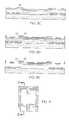
- FIGS. 1A to 1 Eare cross sectional views illustrating one method for forming micromirrors
- FIG. 2is a top view of a micromirror showing line 1 — 1 for taking the cross section for FIGS. 1A to 1 E;
- FIGS. 3A to 3 Eare cross sectional views illustrating the same method as in FIGS. 1A to 1 E but taken along a different cross section;
- FIG. 4is a top view of a mirror showing line 3 — 3 for taking the cross section for FIGS. 3A to 3 E;
- FIG. 5is an isometric view of the assembly of two substrates, one with micromirrors, the other with circuitry and electrodes;
- FIG. 6is a cross sectional view of the assembled device in use
- FIG. 7is a flow chart of one method of the invention.
- FIG. 8is a top view of a wafer substrate having multiple die areas
- FIGS. 9A to 9 Eare step-by-step views of the assembly of the device.
- FIGS. 10A and 10Bare top views of two wafers that will be joined together and then singulated;
- FIGS. 10C and 10Dare views of light transmissive substrates ( FIG. 10A ) for bonding to a wafer ( 10 D);
- FIG. 11Ais a cross sectional view taken along line 11 — 11 of FIG. 10 upon alignment of the two wafers of FIGS. 10A and 10B , but prior to bonding, whereas FIG. 11B is the same cross sectional view after bonding of the two wafers, but prior to singulation;
- FIG. 12is an isometric view of a singulated wafer assembly die held on a package substrate.
- MEMS movable elementse.g. mirrors
- a wafer substratee.g. a light transmissive substrate or a substrate comprising CMOS or other circuitry
- light transmissiveit is meant that the material will be transmissive to light at least in operation of the device (The material could temporarily have a light blocking layer on it to improve the ability to handle the substrate during manufacture, or a partial light blocking layer for decreasing light scatter during use. Regardless, a portion of the substrate, for visible light applications, is preferably transmissive to visible light during use so that light can pass into the device, be reflected by the mirrors, and pass back out of the device. Of course, not all embodiments will use a light transmissive substrate).
- waferit is meant any substrate on which multiple microstructures or microstructure arrays are to be formed and which allows for being divided into dies, each die having one or more microstructures thereon.
- each dieis one device or product to be packaged and sold separately.
- Forming multiple “products” or dies on a larger substrate or waferallows for lower and faster manufacturing costs as compared to forming each die separately.
- the waferscan be any size or shape, though it is preferred that the wafers be the conventional round or substantially round wafers (e.g. 4′′, 6′′ or 12′′ in diameter) so as to allow for manufacture in a standard foundry.
- FIGS. 1A to 1 Eshow a manufacturing process for a micromechanical mirror structure.
- a substratesuch as glass (e.g. 1737F), quartz, PyrexTM, sapphire, (or silicon alone or with circuitry thereon) etc.
- the cross section of FIGS. 1A-Eis taken along line 1 — 1 of FIG. 2 . Because this cross section is taken along the hinge of the movable element, an optional block layer 12 can be provided to block light (incident through the light transmissive substrate during use) from reflecting off of the hinge and potentially causing diffraction and lowering the contrast ratio (if the substrate is transparent).
- a sacrificial layer 14such as amorphous silicon, is deposited.
- the thickness of the sacrificial layercan be wide ranging depending upon the movable element/mirror size and desired tilt angle, though a thickness of from 500 ⁇ to 50,000 ⁇ , preferably around 5000 ⁇ is preferred.
- the sacrificial layercould be a polymer or polyimide (or even polysilicon, silicon nitride, silicon dioxide, etc. depending upon the materials selected to be resistant to the etchant, and the etchant selected).
- a lithography step followed by a sacrificial layer etchforms holes 16 a,b in the sacrificial silicon, which can be any suitable size, though preferably having a diameter of from 0.1 to 1.5 um, more preferably around 0.7+/ ⁇ 0.25 um.
- the etchingis performed down to the glass/quartz substrate or down to the block layer if present. Preferably if the glass/quartz layer is etched, it is in an amount less than 2000 ⁇ .
- a first layer 18is deposited by chemical vapor deposition.
- the materialis silicon nitride or silicon oxide deposited by LPCVD or PECVD, however polysilicon, silicon carbide or an organic compound could be deposited at this point—or Al, CoSiNx, TiSiNx, TaSiNx and other ternary and higher compounds as set forth in U.S. patent application Ser. No. 09/910,537 filed Jul. 20, 2001, and Ser. No. 60/300,533 filed Jun. 22, 2001 both to Reid and incorporated herein by reference (of course the sacrificial layer and etchant should be adapted to the material used).
- the thickness of this first layercan vary depending upon the movable element size and desired amount of stiffness of the element, however in one embodiment the layer has a thickness of from 100 to 3200 ⁇ , more preferably around 1100 ⁇ .
- the first layerundergoes lithography and etching so as to form gaps between adjacent movable elements on the order of from 0.1 to 25 um, preferably around 1 to 2 um.
- a second layer 20(the “hinge” layer) is deposited as can be seen in FIG. 1 D.
- “hinge layer”it is meant the layer that defines that portion of the device that flexes to allow movement of the device.
- the hinge layercan be disposed only for defining the hinge, or for defining the hinge and other areas such as the mirror. In any case, the reinforcing material is removed prior to depositing the hinge material.
- the material for the second (hinge) layercan be the same (e.g.
- silicon nitrideas the first layer or different (silicon oxide, silicon carbide, polysilicon, or Al, CoSiNx, TiSiNx, TaSiNx or other ternary and higher compounds) and can be deposited by chemical vapor deposition as for the first layer.
- the thickness of the second/hinge layercan be greater or less than the first, depending upon the stiffness of the movable element, the flexibility of the hinge desired, the material used, etc.
- the second layerhas a thickness of from 50 ⁇ to 2100 ⁇ , and preferably around 500 ⁇ .
- the first layeris deposited by PECVD and the second layer by LPCVD.
- a reflective and conductive layer 22is deposited.
- the reflective/conductive materialcan be gold, aluminum or other metal, or an alloy of more than one metal though it is preferably aluminum deposited by PVD.
- the thickness of the metal layercan be from 50 to 2000 ⁇ , preferably around 500 ⁇ . It is also possible to deposit separate reflective and conductive layers.
- An optional metal passivation layer(not shown) can be added, e.g. a 10 to 1100 ⁇ silicon oxide layer deposited by PECVD. Then, photoresist patterning on the metal layer is followed by etching through the metal layer with a suitable metal etchant.
- a chlorine (or bromine) chemistrycan be used (e.g.
- both the first and second layersare deposited in the area defining the movable (mirror) element, whereas the second layer, in the absence of the first layer, is deposited in the area of the hinge.
- a plurality of layerscould be provided in place of single layer 18 in FIG. 1C , and a plurality of layers could be provided in place of layer 20 and in place of layer 22 .
- layers 20 and 22could be a single layer, e.g.
- the reinforcing layeris removed in the area of the hinge, followed by depositing the hinge layer and patterning both reinforcing and hinge layer together.
- This joint patterning of the reinforcing layer and hinge layercan be done with the same etchant (e.g. if the two layers are of the same material) or consecutively with different etchants.
- the reinforcing and hinge layerscan be etched with a chlorine chemistry or a fluorine (or other halide) chemistry (e.g. a plasma/RIE etch with F 2 , CF 4 , CHF 3 , C 3 F 8 , CH 2 F 2 , C 2 F 6 , SF 6 , etc.
- the reinforcing layer and the hinge layercan be deposited before the first (reinforcing) and/or second (hinge) layer. Whether deposited prior to the hinge material or prior to both the hinge material and the reinforcing material, it is preferable that the metal be patterned (e.g. removed in the hinge area) prior to depositing and patterning the hinge material.
- FIGS. 3A to 3 Eillustrate the same process taken along a different cross section (cross section 3 — 3 in FIG. 4 ) and show the optional block layer 12 deposited on the light transmissive substrate 10 , followed by the sacrificial layer 14 , layers 18 , 20 and the metal layer 22 .
- the cross sections in FIGS. 1A to 1 E and 3 A to 3 Eare taken along substantially square mirrors in FIGS. 2 and 4 respectively.
- the mirrorsneed not be square but can have other shapes that may decrease diffraction and increase the contrast ratio.
- Such mirrorsare disclosed in U.S. provisional patent application 60/229,246 to Ilkov et al., the subject matter of which is incorporated herein by reference.
- the mirror hingescan be torsion hinges as illustrated in this provisional application.
- a silicon dioxide sacrificial layercould be used and removed with HF (or HF/HCl), or a silicon sacrificial could be removed with ClF3 or BrF3.
- a PSG sacrificial layercould be removed with buffered HF, or an organic sacrificial such as polyimide could be removed in a dry plasma oxygen release step.
- the etchant and sacrificial materialshould be selected depending upon the structural material to be used.
- PVD and CVDare referred to above, other thin film deposition methods could be used for depositing the layers, including spin-on, sputtering, anodization, oxidation, electroplating and evaporation.
- FIGS. 1E and 3Eshow the microstructures in their released state. As can be seen in FIG. 1E , posts 2 hold the released microstructure on substrate 10 .
- each mirrorcan be formed in the same plane as the mirror element (and/or formed as part of the same deposition step) as set forth above, they can also be formed separated from and parallel to the mirror element in a different plane and as part of a separate processing step.
- This superimposed type of hingeis disclosed in FIGS. 11 and 12 of the previously-mentioned U.S. Pat. No. 6,046,840, and in more detail in U.S. patent application “A Deflectable Spatial Light Modulator Having Superimposed Hinge and Deflectable Element” to Huibers et al. filed Aug. 3, 2000, the subject matter of which being incorporated herein.
- the second or “lower” substrate (the backplane) diecontains a large array of electrodes on a top metal layer of the die. Each electrode electrostatically controls one pixel (one micromirror on the upper optically transmissive substrate) of the microdisplay. The voltage on each electrode on the surface of the backplane determines whether its corresponding microdisplay pixel is optically ‘on’ or ‘off,’ forming a visible image on the microdisplay. Details of the backplane and methods for producing a pulse-width-modulated grayscale or color image are disclosed in U.S.
- the display pixels themselvesare binary, always either fully ‘on’ or fully ‘off,’ and so the backplane design is purely digital. Though the micromirrors could be operated in analog mode, no analog capability is necessary.
- the backplane's I/O and control logicpreferably run at a voltage compatible with standard logic levels, e.g. 5V or 3.3V. To maximize the voltage available to drive the pixels, the backplane's array circuitry may run from a separate supply, preferably at a higher voltage.
- One embodiment of the backplanecan be fabricated in a foundry 5V logic process.
- the mirror electrodescan run at 0-5V or as high above 5V as reliability allows.
- the backplanecould also be fabricated in a higher-voltage process such as a foundry Flash memory process using that process's high-voltage devices.
- the backplanecould also be constructed in a high-voltage process with larger-geometry transistors capable of operating at 12V or more.
- a higher voltage backplanecan produce an electrode voltage swing significantly higher than the 5-7V that the lower voltage backplane provides, and thus actuate the pixels more robustly.
- each electrodeIn digital mode, it is possible to set each electrode to either state (on/off), and have that state persist until the state of the electrode is written again.
- a RAM-like structurewith one bit per pixel is one architecture that accomplishes this.
- One exampleis an SRAM-based pixel cell.
- Alternate well-known storage elementssuch as latches or DRAM (pass transistor plus capacitor) are also possible. If a dynamic storage element (e.g. a DRAM-like cell) is used, it is desirable that it be shielded from incident light that might otherwise cause leakage.
- the perception of a grayscale or full-color imagewill be produced by modulating pixels rapidly on and off, for example according to the method in the above-mentioned U.S. patent application Ser. No. 09/564,069 to Richards.
- the backplaneallows the array to be written in random-access fashion, though finer granularity than a row-at-a-time is generally not necessary.
- the diecan be illuminated with a 200W or more arc lamp.
- the thermal and photo-carrier effects of thismay result in special layout efforts to make the metal layers as ‘opaque’ as possible over the active circuitry to reflect incident optical energy and minimize photocarrier and thermal effects.
- An on-chip PN diodecould be included for measuring the temperature of the die.
- the resolutionis XGA, 1024 ⁇ 768 pixels, though other resolutions are possible.
- a pixel pitch of from 5 to 24 umis preferred (e.g. 14 um).
- the size of the electrode array itselfis determined by the pixel pitch and resolution.
- a 14 um XGA device's pixel arraywill therefore be 14.336 ⁇ 10.752 mm.
- the upper and lower wafersare finished being processed (e.g. circuitry/electrodes on lower wafer, micromirrors on upper wafer), the upper and lower wafers are joined together. This joining of the two substrates allows micromirrors on one substrate to be positioned proximate to electrodes on the other substrate. This arrangement is illustrated in FIGS. 5 and 6 , which figures will be described further below.
- the method for the assembly of the wafers and separation of the wafer assembly into individual diesis similar in some ways to the method for assembly of a liquid crystal device as disclosed in U.S. Pat. No. 5,963,289 to Stefanov et al, “Asymmetrical Scribe and Separation Method of Manufacturing Liquid Crystal Devices on Silicon Wafers”, which is hereby incorporated by reference.
- Many bonding methodsare possible such as adhesive bonding (e.g. epoxy, silicone, low K material or other adhesive—described further herein), anodic bonding, compression bonding (e.g. with gold or indium) metal eutectic bonding, solder bonding, fusion bonding, or other wafer bonding processes known in the art.
- the upper and lower waferare made of the same or different materials (silicon, glass, dielectric, multilayer wafer, etc.), they can first be inspected (step 30 in the flow chart of FIG. 7 ) for visual defects, scratches, particles, etc. After inspection, the wafers can be processed through industry standard cleaning processes (step 32 ). These include scrubbing, brushing or ultrasonic cleaning in a solvent, surfactant solution, and/or de-ionized (DI) water.
- DIde-ionized
- the mirrorsare preferably released at this point (step 34 ). Releasing immediately prior to the application of epoxy or bonding is preferable (except for an optional stiction treatment between release and bonding).
- the releasecan be in an atmosphere of xenon difluoride and an optional diluent (e.g. nitrogen and/or helium).
- an optional diluente.g. nitrogen and/or helium
- other etchantscould be used, including interhalogens such as bromine trifluoride and bromine trichloride.
- the releaseis preferably a spontaneous chemical etch which does not require plasma or other external energy to etch the silicon sacrificial layer(s).
- the remainder of the deviceis treated for stiction (step 36 ) by applying an anti-stiction layer (e.g. a self assembled monolayer).
- an anti-stiction layere.g. a self assembled monolayer.
- the layeris preferably formed by placing the device in a liquid or gas silane, preferably a halosilane, and most preferably a chlorosilane.
- silanesare known in the art for their ability to provide anti-stiction for MEMS structures, including the various trichlorsilanes set forth in “Self Assembled Monolayers as Anti-Stiction Coatings for MEMS: Characteristics and Recent Developments”, Maboudian et al., as well as other unfluorinated (or partially or fully fluorinated) alkyl trichlorosilanes, preferably those with a carbon chain of at least 10 carbons, and preferably partially or fully fluorinated. (Tridecafluoro-1,1,2,2-tetrahydro-octyl)trichlorosilane available from Gelest, Inc. is one example.
- spacersare mixed into sealant material (step 38 ).
- Spacers in the form of spheres or rodsare typically dispensed and dispersed between the wafers to provide cell gap control and uniformity and space for mirror deflection. Spacers can be dispensed in the gasket area of the display and therefore mixed into the gasket seal material prior to seal dispensing. This is achieved through normal agitated mixing processes.
- the final target for the gap between the upper and lower wafersis preferably from 1 to 10 um, though other gaps are possible depending upon the MEMS device being formed. This of course depends upon the type of MEMS structure being encapsulated and whether it was surface or bulk micromachined.
- the spheres or rodscan be made of glass or plastic, preferably an elastically deforming material.
- spacer pillarscan be fabricated on at least one of the substrates.
- pillars/spacersare provided only at the side of the array.
- pillars/spacerscan be fabricated in the array itself.
- Other bonding agents with or without spacerscould be used, including anodic bonding or metal compression bonding with a patterned eutectic or metal.
- a gasket seal materialcan then be dispensed (step 40 ) on the bottom substrate in a desired pattern, usually in one of two industry standard methods including automated controlled liquid dispensing through a syringe and printing (screen, offset, or roller).
- automated controlled liquid dispensingthrough a syringe and printing (screen, offset, or roller).
- a syringeWhen using a syringe, it is moved along X-Y coordinates relative to the parts.
- the syringe tipis constrained to be just above the part with the gasket material forced through the needle by positive pressure.
- Positive pressureis provided either by a mechanical plunger forced by a gear driven configuration and/or by an air piston and/or pressed through the use of an auger.
- This dispensing methodprovides the highest resolution and process control but provides less throughput.
- the two wafersare aligned (step 42 ).
- Alignment of the opposing electrodes or active viewing areasrequires registration of substrate fiducials on opposite substrates. This task is usually accomplished with the aid of video cameras with lens magnification.
- the machinesrange in complexity from manual to fully automated with pattern recognition capability. Whatever the level of sophistication, they accomplish the following process: 1. Dispense a very small amount of a UV curable adhesive at locations near the perimeter and off of all functional devices in the array; 2. Align the fiducials of the opposing substrates within the equipment capability; and 3. Press substrates and UV tack for fixing the wafer to wafer alignment through the remaining bonding process (e.g., curing of the internal epoxy).
- the final cell gapcan be set by pressing (step 44 ) the previously tacked laminates in a UV or thermal press.
- a UV pressa common procedure would have the substrates loaded into a press where at least one or both of the press platens are quartz, in order to allow UV radiation from a UV lamp to pass unabated to the gasket seal epoxy.
- Exposure time and flux ratesare process parameters determined by the equipment and adhesive materials.
- Thermally cured epoxiesrequire that the top and bottom platens of a thermal press be heated. The force that can be generated between the press platens is typically many pounds. With thermally cured epoxies, after the initial press the arrays are typically transferred to a stacked press fixture where they can continue to be pressed and post-cured for 4-8 hours.
- the assemblycan be separated into individual dies (step 46 ). Silicon substrate and glass scribes are placed on the respective substrates in an offset relationship at least along one direction. The units are then separated, resulting in each unit having a bond pad ledge on one side and a glass electrical contact ledge on an opposite side.
- the partsmay be separated from the array by any of the following methods.
- the order in which the array (glass first) substrate is scribedis important when conventional solid state cameras are used for viewing and alignment in a scribe machine. This constraint exists unless special infrared viewing cameras are installed which make the silicon transparent and therefore permits viewing of front surface metal fiducials.
- the scribe toolis aligned with the scribe fiducials and processed.
- the resultant scribe lines in the glassare used as reference marks to align the silicon substrate scribe lanes. These scribe lanes may be coincident with the glass substrate scribes or uniformly offset.
- the partsare then separated from the array by venting the scribes on both substrates. Automatic breaking is done by commercially available guillotine or fulcrum breaking machines. The parts can also be separated by hand.
- Separationmay also by done by glass scribing and partial sawing of the silicon substrate.
- Sawingrequires an additional step at gasket dispense. Sawing is done in the presence of a high-pressure jet of water. Moisture must not be allowed in the area of the fill port or damage of the MEMS structures could occur. Therefore, at gasket dispense, an additional gasket bead must be dispensed around the perimeter of the wafer.
- the end of each scribe/saw lanemust be initially left open, to let air vent during the align and press processes. After the array has been pressed and the gasket material cured, the vents are then closed using either the gasket or end-seal material.
- the glassis then aligned and scribed as described above. Sawing of the wafer is done from the backside of the silicon where the saw streets are aligned relative to the glass scribe lanes described above. The wafer is then sawed to a depth of 50%-90% of its thickness. The parts are then separated as described above.
- both the glass and silicon substratesmay be partially sawed prior to part separation.
- vent and seal processes as described abovesaw lanes are aligned to fiducials on the glass substrates.
- the glassis sawed to a depth between 50% and 95% of its thickness.
- the silicon substrateis sawed and the parts separated as described above.
- each die area 3(having a length A and a height B) comprises one or more (preferably released) microstructures.
- each diepreferably has at least 1000 movable mirrors, and more likely between 1 and 6 million movable elements.
- the microstructureis a DC relay or RF MEMS switch (or even mirrors for an optical switch) there will likely be far fewer than millions of microstructures, more likely less than 100 or even less than 10 (or even a single structure).
- the die areasthemselves can be made smaller in most cases.
- the die areasneed not be rectangular, though this shape aids in epoxy deposition and singulation.
- each die area 3 a to 3 dcomprises one or more microstructures which have already been released in a suitable etchant.
- epoxycan be applied in the form of beads 31 a to 31 d along each side of the die area, or as beads 32 a to 32 d at each corner of the die area.
- epoxy ribbons 33 a and 33 bcould be applied along two sides of each die, or a single ribbon 34 could be applied substantially surrounding an entire die.
- the dienot be fully surrounded with an epoxy gasket as this will prevent air or other gas from escaping when the two wafers are pressed together during a full or partial epoxy cure.
- a common epoxy application methodthroughout the entire wafer (the different types of applications in FIG. 9B are for illustrations purposes only).
- the areas in which epoxy is appliedcan first have a sacrificial material deposited in that area (preferably in an area larger than the bead or band of epoxy due to expansion of the epoxy under compression).
- the sacrificial materialcould also be applied to the entire wafer except in areas having microstructures thereon.
- a conductive epoxy(or other adhesive) could be used in order to make electrical contact between the wafer having circuitry and electrodes and the wafer having MEMS thereon.
- the sealing wafer 25 and the lower substrate wafer 5 with microstructures (and optionally circuitry)are brought into contact with each other.
- the final gap between the two waferscan be any size that allows the two wafers to be held together and singulated uniformly. Because gasket beads will expand upon application of pressure (thus taking up valuable real estate on a wafer with densely positioned die areas), it is preferable that the gap size be larger than 1 um, and preferably greater than 10 um.
- the gap sizecan be regulated by providing microfabricated spacers or spacers mixed in with the epoxy (e.g. 25 um spacers). However, spacers may not be necessary depending upon the type of microstructure and the amount of pressure applied.
- FIG. 9Dshows the first wafer 5 and sealing wafer 25 bonded together.
- Horizontal and vertical score or partial saw lines 21 a and 21 bare provided on both the sealing wafer 25 and the first (lower) wafer 5 (lines not shown on wafer 5 ).
- the score lines on the two wafersare offset slightly from each other at least in one of the (horizontal or vertical). This offset scoring or partial sawing allows for ledges on each die when the wafer is completely singulated into individual dies (see FIG. 9 E).
- Electrical connections 4 on ledge 6 on die 3 callow for electrical testing of the die prior to removal of the sealing wafer portion. Should the die fail the electrical testing of the microstructures, the sealing wafer need not be removed and the entire die can be discarded.
- FIG. 5a top perspective view of a portion of a bonded wafer assembly die 10 is illustrated.
- the mirror shapes illustrated in FIGS. 1-5are exemplary, as many other mirror structures are possible, such as set forth in U.S. patent application Ser. No. 09/732,445 to Ilkov et al. filed Dec. 7, 2000, incorporated herein by reference.
- the pixel cells 54 , 54 a , 54 b and 54 chave a pixel pitch of, for example, 12 microns. “Pixel pitch” is defined as the distance between like portions of neighboring pixel cells.
- Reflective deflectable elementse.g., mirrors 48 , 48 a , 48 b and 48 c ), each corresponding to a respective pixel cell 54 , 54 a , 54 b and 54 c , are attached to the lower surface 14 of the optically transmissive substrate 52 in an undeflected position.
- mirrors 48 , 48 a , 48 b and 48 care visible through optically transmissive substrate 52 in FIG. 5 .
- light blocking aperture layers 56if present, between the mirrors 48 , 48 a , 48 b or 48 c and the optically transmissive substrate 52 , are represented only by dashed lines so as to show underlying hinges 50 , 50 a , 50 b and 50 c .
- the distance separating neighboring mirrorsmay be, for example, 0.5 microns or less.
- the optically transmissive substrate 52is made of materials which can withstand subsequent processing temperatures.
- the optically transmissive substrate 52may be, for example, a 4 inch quartz wafer 500 microns thick. Such quartz wafers are widely available from, for example, Hoya Corporation U.S.A at 960 Rincon Circle, San Jose, Calif. 95131.
- the substratecan be glass such as Corning 1737 or Corning Eagle2000 or other suitable optically transmissive substrate.
- the substrateis transmissive to visible light, and can be display grade glass.
- the light transmissive substrate 52is bonded to e.g. a MOS-type substrate 62 in spaced apart relation due to spacers 44 .
- a plurality of electrodes 63are disposed adjacent a plurality of micromirrors 64 (mirrors simplified and only 9 illustrated for convenience) for electrostatically deflecting the micromirrors.
- An incoming light beam 65 awill be reflected by a non-deflected mirror at the same angle as it is incident, but will be deflected “vertically” as outgoing light beam 65 b when the mirror is deflected.
- a color sequencerwheel or prism
- the method for forming micromirrors as set forth aboveis but one example of many methods for forming many different MEMS devices (whether with or without an electrical component), in accordance with the present invention.
- the electrical component of the final MEMS deviceis formed on a separate wafer than the micromirrors in the above example, it is also possible to form the circuitry and micromechanical structures monolithically on the same substrate.
- the method for forming the MEMS structurescould be similar to that described in FIGS. 1-4 if the microstructures are micromirrors (with the difference being that the mirrors are formed on the substrate after forming circuitry and electrodes). Or, other methods for forming circuitry and micromirrors monolithically on the same substrate as known in the art could be used.
- FIGS. 10A and 10Bshow two wafers that will be joined together and then singulated.
- FIG. 10Ais a top view of a light transmissive cover wafer (having a mask area, getter area, lubricant area and compression metal bonding area)
- FIG. 10Bis an illustration of such a monolithically formed mirror array (e.g. for a spatial light modulator) on a bottom semiconductor wafer (along with a metal area for compression bonding).
- a plurality of mirror arrays 71 a to 71 eare formed on a “bottom” wafer 70 (e.g. a silicon wafer).
- a metal for compression bondingis applied (areas 73 a to 73 e ) around each mirror array.
- more arrayscould be formed on the wafer (as shown in FIG. 8 ).
- a “top” wafer 80e.g. glass or quartz—preferably display grade glass
- masks 81 a-ewhich will block visible light around a perimeter area of each die from reaching the mirror arrays after the two wafers are bonded and singulated.
- Also illustrated in FIG. 10Aare areas of lubricant 83 a-e , areas of getter material 85 a-e , and areas of metal for compression bonding 87 a-e . If the wafer of FIG.
- a lubricant on the wafer of FIG. 10Amay be omitted if desired (although multiple applications of lubricants can be provided).
- the lubricant applied to the wafer as a gasket, band or drop on the wafercan be any suitable lubricant, such as the various liquid or solid organic (or hybrid organic-inorganic materials) set forth in U.S. Pat. Nos. 5,694,740 5,512,374, 6,024,801, and 5,939,785, each of these being incorporated herein by reference.
- a trichlorosilane SAMis applied to the entire wafer or large portions of the wafer at least covering the micromechanical elements, and a silicone is applied to the lubricant areas 83 a-e .
- the metal for compression bondingcould be any suitable metal for this purpose such as gold or indium.
- the adhesivecould be any suitable adhesive, such as an epoxy or silicone adhesive, and preferably an adhesive with low outgassing.
- any combination of these elementscould be present (or none at all if the bonding method is other than an adhesive bonding method).
- one or more of the mask, lubricant, getter and bonding materialare present on the “top” wafer 80 prior to bonding.
- the lubricant, getter and bonding materialcould be applied to only the top or bottom wafer or both wafers. In an alternate embodiment, it may be desirable to apply the lubricant and getter to the bottom wafer around the circuitry and electrodes, with bonding material on both wafers.
- the maskor the lubricant or getter
- the bands of lubricant, getter and bonding materialneed not fully encircle the “die area” on the wafer, but could be applied in strips of dots as illustrated in FIG. 9 B.
- the bonding materialdoes not fully encircle the MEMS die area, then, prior to singulation, it is preferred that the bonding material “gap” be filled so as to protect the MEMS devices during singulation (from particulate and/or liquid damage depending upon the singulation method).
- substrates 101 a-dare substrates transmissive to visible light and have thereon masks 81 a-d as well as areas of lubricant 83 a-d , areas of getter material 85 a-d , and areas of bonding material 87 a-d (e.g. gold or indium for metal compression bonding.
- the mask areasare preferably “picture frame” shaped rectangular areas that block the transmission of visible light. This arrangement is desirable for selectively blocking light incident on micromirror arrays formed on the wafer. After bonding the multiple substrates with mask areas to the wafer, the wafer is singulated into wafer assembly portions, followed by packaging such as in FIG. 12 .
- the MEMS waferscould be made of any suitable material, depending upon the final application for the devices, including silicon, glass, quartz, alumina, GaAs, etc. Silicon wafers can typically be processed to include circuitry.
- the “top” wafer of FIG. 10Ais preferably transparent, as mentioned above.
- the mask illustrated in FIG. 10Acan be an absorptive or reflective mask, such as one made from TiN, AlN, or other oxide or nitride compound, or polymers or other suitable materials having sufficient light blocking capabilities.
- This “top” wafercould also incorporate other optical elements, such as lenses, UV or other types of filters or antireflection and/or antiscratch coatings.
- FIG. 11Ais a cross section taken along line 11 — 11 in FIG. 10A (after alignment with bottom wafer 70 in FIG. 10 B), whereas FIG. 10B is the same cross section after bonding (but before singulation).
- FIG. 12is an illustration of a packaged wafer assembly portion after singulation of the bonded wafers. As can be seen in FIG. 12 , a lower substrate 94 is bonded to the upper substrate 93 , with the lower substrate held on a lower packaging substrate 90 .
- Metal areas 96 on lower wafer portion 94will be electrically connected to metal areas 97 on the package substrate 90 .
- This packagingcan be desirable for a monolithic MEMS device where both the circuitry and MEMS elements are on the same substrate, as well as where the MEMS elements are formed on a substrate different from the circuitry.
- epoxycan be applied to the one or both of the upper and lower wafers.
- epoxyis applied to both the circumference of the wafer and completely or substantially surrounding each die/array on the wafer.
- Spacerscan be mixed in the epoxy so as to cause a predetermined amount of separation between the wafers after bonding. Such spacers hold together the upper and lower wafers in spaced-apart relation to each other. The spacers act to hold the upper and lower wafers together and at the same time create a space in which the movable mirror elements can move.
- the spacer layercould comprise walls or protrusions that are micro-fabricated.
- one or more waferscould be bonded between the upper and lower wafers and have portions removed (e.g. by etching) in areas corresponding to each mirror array (thereby providing space for deflection of the movable elements in the array).
- the portions removed in such intermediate waferscould be removed prior to alignment and bonding between the upper and lower wafers, or, the wafer(s) could be etched once bonded to either the upper or lower wafer.
- the spacersare micro-fabricated spacers, they can be formed on the lower wafer, followed by the dispensing of an epoxy, polymer, or other adhesive (e.g. a multi-part epoxy, or a heat or UV-cured adhesive) adjacent to the micro-fabricated spacers.
- the adhesive and spacersneed not be co-located, but could be deposited in different areas on the lower substrate wafer.
- a compression bond materialcould be used that would allow for adhesion of the upper and lower wafers.
- the spacerscould be balls or rods of a predetermined size that are within the adhesive when the adhesive is placed on the lower wafer.
- Spacers provided within the adhesivecan be made of glass or plastic, or even metal so long as the spacers do not interfere with the electrostatic actuation of the movable element in the upper wafer.
- the spacersare preferably from 1 to 250 microns, the size in large part depending upon the size of the movable mirror elements and the desired angle of deflection.
- the spacer size in the direction orthogonal to the plane of the upper and lower wafersis more preferably from 1 to 100 microns, with some applications benefiting from a size in the range of from 1 to 20 microns, or even less than 10 microns.
- a sticking force reducing agentcan be applied to the microstructures (micromirrors, microrelays, etc) on the wafer to reduce adhesion forces upon contact of the microstructures with another layer or structure on the same or opposing substrate.
- adhesion reducing agentsare known, in the present invention the agent is preferably applied to the wafer before wafer bonding (or after wafer bonding but before singulation), rather than to the singulated die or package for the die.
- Various adhesion reducing agentsincluding various trichlorosilanes, and other silanes and siloxanes as known in the art for reducing stiction for micro electromechanical devices, as mentioned elsewhere herein.
- a getter or molecular scavengercan be applied to the wafer prior to wafer bonding as mentioned above.
- the gettercan be a moisture, hydrogen, particle or other getter.
- the getter(s)is applied to the wafer around the released MEMS structures (or around, along or adjacent an array of such structures, e.g. in the case of a micromirror array), of course preferably not being in contact with the released structures.
- a metal oxide or zeolitecan be the material utilized for absorbing and binding water (e.g. StayDry SD800, StayDry SD1000, StayDry HiCap2000—each from Cookson Electronics).
- a combination gettercould be used, such as a moisture and particle getter (StayDry GA2000-2) or a hydrogen and moisture getter (StayDry H2-3000).
- the gettercan be applied to either wafer, and if adhesive bonding is the bonding method, the getter can be applied adjacent the epoxy beads or strips, preferably between the epoxy and the microstructures, and can be applied before or after application of the adhesive (preferably before any adhesive is applied to the wafer(s).
- the method of the present inventioncomprises making a MEMS device, e.g. a spatial light modulator, by providing a first wafer, providing a second wafer, forming circuitry and a plurality of electrodes on the first wafer, forming a plurality of deflectable elements on or in either the first or second wafer, aligning the first and second wafers, bonding the first and second wafers together to form a wafer assembly, separating the wafer assembly into individual dies, and packaging the individual dies.
- Each diecan comprise an array of deflectable reflective elements.
- the reflective elementscorrespond to pixels in a direct-view or projection display.
- the number of reflective elements in each dieis from 6,000 to about 6 million, depending upon the resolution of the display.
- the first waferis preferably glass, borosilicate, tempered glass, quartz or sapphire, or can be a light transmissive wafer of another material.
- the second wafercan be a dielectric or semiconductor wafer, e.g. GaAs or silicon.
- the first and second wafersare bonded together with an adhesive (thought metal or anodic bonding are also possible, depending upon the MEMS structure and the type of micromachining.
- the releasingcan be performed by providing any suitable etchant, including an etchant selected from an interhalogen, a noble gas fluoride, a vapor phase acid, or a gas solvent. And, the releasing is preferably followed by a stiction treatment (e.g. a silane, such as a chlorosilane). Also, a getter can be applied to the wafer before or after the adhesion reducing agent is applied, and before or after an adhesive is applied (if an adhesive bonding method is chosen). Preferably the time from releasing to bonding is less than 12 hours, and preferably less than 6 hours.
- a stiction treatmente.g. a silane, such as a chlorosilane
- a gettercan be applied to the wafer before or after the adhesion reducing agent is applied, and before or after an adhesive is applied (if an adhesive bonding method is chosen).
- the time from releasing to bondingis less than 12 hours, and preferably less than 6 hours.
- each die defining a mirror array(or other MEMS device) is already packaged and sealed from possible contamination, physical damage, etc.
- the mirrorsare still exposed and remain exposed while sent to packaging to finally be enclosed and protected (e.g. under a glass panel).
- the inventionneed not be limited to a direct-view or projection display.
- the inventionis applicable to many different types of MEMS devices, including pressure and acceleration sensors, MEMS switches or other MEMS devices formed and released on a wafer.
- the inventionalso need not be limited to forming the releasable MEMS elements on one wafer and circuitry on another wafer. If both MEMS and circuitry are formed monolithically on the same wafer, a second wafer (glass, silicon or other material) can be attached at the wafer lever following release of the MEMS devices but prior to dividing the wafers into individual dies. This can be particularly useful if the MEMS devices are micromirrors, due to the fragility of such elements.
- MEMS deviceis a mirror
- the particular mirror shapes disclosed in U.S. patent application Ser. No. 09/732,445 to Ilkov et al. filed Dec. 7, 2000could be used.
- the MEMS deviceneed not be a micromirror, but could instead be any MEMS device, including those disclosed in the above applications and in application Ser. No. 60/240,552 to Huibers filed Dec.
Landscapes
- Engineering & Computer Science (AREA)
- Microelectronics & Electronic Packaging (AREA)
- Manufacturing & Machinery (AREA)
- Chemical & Material Sciences (AREA)
- Physics & Mathematics (AREA)
- General Physics & Mathematics (AREA)
- Computer Hardware Design (AREA)
- Nanotechnology (AREA)
- Power Engineering (AREA)
- Optics & Photonics (AREA)
- Composite Materials (AREA)
- Condensed Matter Physics & Semiconductors (AREA)
- Materials Engineering (AREA)
- Crystallography & Structural Chemistry (AREA)
- Mechanical Light Control Or Optical Switches (AREA)
- Micromachines (AREA)
Abstract
Description
Claims (134)
Priority Applications (26)
| Application Number | Priority Date | Filing Date | Title |
|---|---|---|---|
| US10/005,308US6969635B2 (en) | 2000-12-07 | 2001-12-03 | Methods for depositing, releasing and packaging micro-electromechanical devices on wafer substrates |
| US10/099,314US6900072B2 (en) | 2001-03-15 | 2002-03-15 | Method for making a micromechanical device by using a sacrificial substrate |
| PCT/US2002/007761WO2002075794A2 (en) | 2001-03-15 | 2002-03-15 | A method for making a micromechanical device by using a sacrificial substrate |
| US10/167,361US7307775B2 (en) | 2000-12-07 | 2002-06-11 | Methods for depositing, releasing and packaging micro-electromechanical devices on wafer substrates |
| US10/305,631US6952301B2 (en) | 1995-06-19 | 2002-11-26 | Spatial light modulators with light blocking and absorbing areas |
| US10/305,536US6906847B2 (en) | 2000-12-07 | 2002-11-26 | Spatial light modulators with light blocking/absorbing areas |
| US10/402,777US6960305B2 (en) | 1999-10-26 | 2003-03-28 | Methods for forming and releasing microelectromechanical structures |
| US10/930,342US6995034B2 (en) | 2000-12-07 | 2004-08-30 | Methods for depositing, releasing and packaging micro-electromechanical devices on wafer substrates |
| US10/930,450US20050048688A1 (en) | 2000-12-07 | 2004-08-30 | Methods for depositing, releasing and packaging micro-electromechanical devices on wafer substrates |
| US11/070,036US20050139940A1 (en) | 2000-12-07 | 2005-03-01 | Methods for depositing, releasing and packaging microelectromechanical devices on wafer substrates |
| US11/093,550US7198982B2 (en) | 2000-12-07 | 2005-03-29 | Methods for depositing, releasing and packaging micro-electromechanical devices on wafer substrates |
| US11/093,943US6995040B2 (en) | 2000-12-07 | 2005-03-29 | Methods for depositing, releasing and packaging micro-electromechanical devices on wafer substrates |
| US11/094,087US7586668B2 (en) | 2000-12-07 | 2005-03-29 | Methods for depositing, releasing and packaging micro-electromechanical devices on wafer substrates |
| US11/094,086US7629190B2 (en) | 2001-03-15 | 2005-03-29 | Method for making a micromechanical device by using a sacrificial substrate |
| US11/093,927US7449358B2 (en) | 2000-12-07 | 2005-03-29 | Methods for depositing, releasing and packaging micro-electromechanical devices on wafer substrates |
| US11/093,942US20050170557A1 (en) | 2000-12-07 | 2005-03-29 | Methods for depositing, releasing and packaging micro-electromechanical devices on wafer substrates |
| US11/102,204US7286278B2 (en) | 2000-12-07 | 2005-04-07 | Methods for depositing, releasing and packaging micro-electromechanical devices on wafer substrates |
| US11/102,214US20050260793A1 (en) | 2000-12-07 | 2005-04-07 | Methods for depositing, releasing and packaging micro-electromechanical devices on wafer substrates |
| US11/102,295US20050191790A1 (en) | 2000-12-07 | 2005-04-07 | Methods for depositing, releasing and packaging micro-electromechanical devices on wafer substrates |
| US11/102,187US20050179982A1 (en) | 2000-12-07 | 2005-04-07 | Methods for depositing, releasing and packaging micro-electromechanical devices on wafer substrates |
| US11/102,291US20050191789A1 (en) | 2000-12-07 | 2005-04-07 | Methods for depositing, releasing and packaging micro-electromechanical devices on wafer substrates |
| US11/102,108US20050214976A1 (en) | 2000-12-07 | 2005-04-07 | Methods for depositing, releasing and packaging micro-electromechanical devices on wafer substrates |
| US11/102,183US7655492B2 (en) | 2000-12-07 | 2005-04-07 | Methods for depositing, releasing and packaging micro-electromechanical devices on wafer substrates |
| US11/101,939US7573111B2 (en) | 2000-12-07 | 2005-04-07 | Methods for depositing, releasing and packaging micro-electromechanical devices on wafer substrates |
| US11/102,186US7671428B2 (en) | 2000-12-07 | 2005-04-07 | Methods for depositing, releasing and packaging micro-electromechanical devices on wafer substrates |
| US11/954,076US20080096313A1 (en) | 2000-12-07 | 2007-12-11 | Methods for Depositing, Releasing and Packaging Micro-Electromechanical Devices on Wafer Substrates |
Applications Claiming Priority (3)
| Application Number | Priority Date | Filing Date | Title |
|---|---|---|---|
| US25404300P | 2000-12-07 | 2000-12-07 | |
| US27622201P | 2001-03-15 | 2001-03-15 | |
| US10/005,308US6969635B2 (en) | 2000-12-07 | 2001-12-03 | Methods for depositing, releasing and packaging micro-electromechanical devices on wafer substrates |
Related Parent Applications (3)
| Application Number | Title | Priority Date | Filing Date |
|---|---|---|---|
| US09/624,591ContinuationUS6356378B1 (en) | 1995-06-19 | 2000-07-24 | Double substrate reflective spatial light modulator |
| PCT/US2001/024332Continuation-In-PartWO2002012925A2 (en) | 1998-09-24 | 2001-08-03 | Micromirror elements, package for the micromirror elements, and protection system therefor |
| US10343307Continuation-In-Part | 2001-08-03 |
Related Child Applications (24)
| Application Number | Title | Priority Date | Filing Date |
|---|---|---|---|
| US09/637,479Continuation-In-PartUS6396619B1 (en) | 1999-10-26 | 2000-08-11 | Deflectable spatial light modulator having stopping mechanisms |
| US10/043,703Continuation-In-PartUS6538800B2 (en) | 1995-06-19 | 2002-01-09 | Reflective spatial light modulator with deflectable elements formed on a light transmissive substrate |
| US10/099,314Continuation-In-PartUS6900072B2 (en) | 2001-03-15 | 2002-03-15 | Method for making a micromechanical device by using a sacrificial substrate |
| US10/167,361Continuation-In-PartUS7307775B2 (en) | 2000-12-07 | 2002-06-11 | Methods for depositing, releasing and packaging micro-electromechanical devices on wafer substrates |
| US10/305,536Continuation-In-PartUS6906847B2 (en) | 2000-12-07 | 2002-11-26 | Spatial light modulators with light blocking/absorbing areas |
| US10/402,777Continuation-In-PartUS6960305B2 (en) | 1999-10-26 | 2003-03-28 | Methods for forming and releasing microelectromechanical structures |
| US10/930,450DivisionUS20050048688A1 (en) | 2000-12-07 | 2004-08-30 | Methods for depositing, releasing and packaging micro-electromechanical devices on wafer substrates |
| US10/930,342ContinuationUS6995034B2 (en) | 2000-12-07 | 2004-08-30 | Methods for depositing, releasing and packaging micro-electromechanical devices on wafer substrates |
| US11/070,036ContinuationUS20050139940A1 (en) | 2000-12-07 | 2005-03-01 | Methods for depositing, releasing and packaging microelectromechanical devices on wafer substrates |
| US11/093,927ContinuationUS7449358B2 (en) | 2000-12-07 | 2005-03-29 | Methods for depositing, releasing and packaging micro-electromechanical devices on wafer substrates |
| US11/093,550ContinuationUS7198982B2 (en) | 2000-12-07 | 2005-03-29 | Methods for depositing, releasing and packaging micro-electromechanical devices on wafer substrates |
| US11/094,086Continuation-In-PartUS7629190B2 (en) | 2001-03-15 | 2005-03-29 | Method for making a micromechanical device by using a sacrificial substrate |
| US11/094,087ContinuationUS7586668B2 (en) | 2000-12-07 | 2005-03-29 | Methods for depositing, releasing and packaging micro-electromechanical devices on wafer substrates |
| US11/093,943ContinuationUS6995040B2 (en) | 2000-12-07 | 2005-03-29 | Methods for depositing, releasing and packaging micro-electromechanical devices on wafer substrates |
| US11/093,942ContinuationUS20050170557A1 (en) | 2000-12-07 | 2005-03-29 | Methods for depositing, releasing and packaging micro-electromechanical devices on wafer substrates |
| US11/102,214ContinuationUS20050260793A1 (en) | 2000-12-07 | 2005-04-07 | Methods for depositing, releasing and packaging micro-electromechanical devices on wafer substrates |
| US11/102,183ContinuationUS7655492B2 (en) | 2000-12-07 | 2005-04-07 | Methods for depositing, releasing and packaging micro-electromechanical devices on wafer substrates |
| US11/102,187ContinuationUS20050179982A1 (en) | 2000-12-07 | 2005-04-07 | Methods for depositing, releasing and packaging micro-electromechanical devices on wafer substrates |
| US11/102,291ContinuationUS20050191789A1 (en) | 2000-12-07 | 2005-04-07 | Methods for depositing, releasing and packaging micro-electromechanical devices on wafer substrates |
| US11/102,204ContinuationUS7286278B2 (en) | 2000-12-07 | 2005-04-07 | Methods for depositing, releasing and packaging micro-electromechanical devices on wafer substrates |
| US11/101,939ContinuationUS7573111B2 (en) | 2000-12-07 | 2005-04-07 | Methods for depositing, releasing and packaging micro-electromechanical devices on wafer substrates |
| US11/102,108ContinuationUS20050214976A1 (en) | 2000-12-07 | 2005-04-07 | Methods for depositing, releasing and packaging micro-electromechanical devices on wafer substrates |
| US11/102,186ContinuationUS7671428B2 (en) | 2000-12-07 | 2005-04-07 | Methods for depositing, releasing and packaging micro-electromechanical devices on wafer substrates |
| US11/102,295ContinuationUS20050191790A1 (en) | 2000-12-07 | 2005-04-07 | Methods for depositing, releasing and packaging micro-electromechanical devices on wafer substrates |
Publications (2)
| Publication Number | Publication Date |
|---|---|
| US20030054588A1 US20030054588A1 (en) | 2003-03-20 |
| US6969635B2true US6969635B2 (en) | 2005-11-29 |
Family
ID=26674189
Family Applications (18)
| Application Number | Title | Priority Date | Filing Date |
|---|---|---|---|
| US10/005,308Expired - LifetimeUS6969635B2 (en) | 1995-06-19 | 2001-12-03 | Methods for depositing, releasing and packaging micro-electromechanical devices on wafer substrates |
| US10/099,314Expired - LifetimeUS6900072B2 (en) | 2001-03-15 | 2002-03-15 | Method for making a micromechanical device by using a sacrificial substrate |
| US11/070,036AbandonedUS20050139940A1 (en) | 2000-12-07 | 2005-03-01 | Methods for depositing, releasing and packaging microelectromechanical devices on wafer substrates |
| US11/093,943Expired - LifetimeUS6995040B2 (en) | 2000-12-07 | 2005-03-29 | Methods for depositing, releasing and packaging micro-electromechanical devices on wafer substrates |
| US11/093,927Expired - LifetimeUS7449358B2 (en) | 2000-12-07 | 2005-03-29 | Methods for depositing, releasing and packaging micro-electromechanical devices on wafer substrates |
| US11/094,087Expired - LifetimeUS7586668B2 (en) | 2000-12-07 | 2005-03-29 | Methods for depositing, releasing and packaging micro-electromechanical devices on wafer substrates |
| US11/094,086Expired - LifetimeUS7629190B2 (en) | 2001-03-15 | 2005-03-29 | Method for making a micromechanical device by using a sacrificial substrate |
| US11/093,942AbandonedUS20050170557A1 (en) | 2000-12-07 | 2005-03-29 | Methods for depositing, releasing and packaging micro-electromechanical devices on wafer substrates |
| US11/093,550Expired - LifetimeUS7198982B2 (en) | 2000-12-07 | 2005-03-29 | Methods for depositing, releasing and packaging micro-electromechanical devices on wafer substrates |
| US11/102,204Expired - LifetimeUS7286278B2 (en) | 2000-12-07 | 2005-04-07 | Methods for depositing, releasing and packaging micro-electromechanical devices on wafer substrates |
| US11/102,295AbandonedUS20050191790A1 (en) | 2000-12-07 | 2005-04-07 | Methods for depositing, releasing and packaging micro-electromechanical devices on wafer substrates |
| US11/101,939Expired - LifetimeUS7573111B2 (en) | 2000-12-07 | 2005-04-07 | Methods for depositing, releasing and packaging micro-electromechanical devices on wafer substrates |
| US11/102,183Expired - LifetimeUS7655492B2 (en) | 2000-12-07 | 2005-04-07 | Methods for depositing, releasing and packaging micro-electromechanical devices on wafer substrates |
| US11/102,186Expired - Fee RelatedUS7671428B2 (en) | 2000-12-07 | 2005-04-07 | Methods for depositing, releasing and packaging micro-electromechanical devices on wafer substrates |
| US11/102,291AbandonedUS20050191789A1 (en) | 2000-12-07 | 2005-04-07 | Methods for depositing, releasing and packaging micro-electromechanical devices on wafer substrates |
| US11/102,214AbandonedUS20050260793A1 (en) | 2000-12-07 | 2005-04-07 | Methods for depositing, releasing and packaging micro-electromechanical devices on wafer substrates |
| US11/102,187AbandonedUS20050179982A1 (en) | 2000-12-07 | 2005-04-07 | Methods for depositing, releasing and packaging micro-electromechanical devices on wafer substrates |
| US11/102,108AbandonedUS20050214976A1 (en) | 2000-12-07 | 2005-04-07 | Methods for depositing, releasing and packaging micro-electromechanical devices on wafer substrates |
Family Applications After (17)
| Application Number | Title | Priority Date | Filing Date |
|---|---|---|---|
| US10/099,314Expired - LifetimeUS6900072B2 (en) | 2001-03-15 | 2002-03-15 | Method for making a micromechanical device by using a sacrificial substrate |
| US11/070,036AbandonedUS20050139940A1 (en) | 2000-12-07 | 2005-03-01 | Methods for depositing, releasing and packaging microelectromechanical devices on wafer substrates |
| US11/093,943Expired - LifetimeUS6995040B2 (en) | 2000-12-07 | 2005-03-29 | Methods for depositing, releasing and packaging micro-electromechanical devices on wafer substrates |
| US11/093,927Expired - LifetimeUS7449358B2 (en) | 2000-12-07 | 2005-03-29 | Methods for depositing, releasing and packaging micro-electromechanical devices on wafer substrates |
| US11/094,087Expired - LifetimeUS7586668B2 (en) | 2000-12-07 | 2005-03-29 | Methods for depositing, releasing and packaging micro-electromechanical devices on wafer substrates |
| US11/094,086Expired - LifetimeUS7629190B2 (en) | 2001-03-15 | 2005-03-29 | Method for making a micromechanical device by using a sacrificial substrate |
| US11/093,942AbandonedUS20050170557A1 (en) | 2000-12-07 | 2005-03-29 | Methods for depositing, releasing and packaging micro-electromechanical devices on wafer substrates |
| US11/093,550Expired - LifetimeUS7198982B2 (en) | 2000-12-07 | 2005-03-29 | Methods for depositing, releasing and packaging micro-electromechanical devices on wafer substrates |
| US11/102,204Expired - LifetimeUS7286278B2 (en) | 2000-12-07 | 2005-04-07 | Methods for depositing, releasing and packaging micro-electromechanical devices on wafer substrates |
| US11/102,295AbandonedUS20050191790A1 (en) | 2000-12-07 | 2005-04-07 | Methods for depositing, releasing and packaging micro-electromechanical devices on wafer substrates |
| US11/101,939Expired - LifetimeUS7573111B2 (en) | 2000-12-07 | 2005-04-07 | Methods for depositing, releasing and packaging micro-electromechanical devices on wafer substrates |
| US11/102,183Expired - LifetimeUS7655492B2 (en) | 2000-12-07 | 2005-04-07 | Methods for depositing, releasing and packaging micro-electromechanical devices on wafer substrates |
| US11/102,186Expired - Fee RelatedUS7671428B2 (en) | 2000-12-07 | 2005-04-07 | Methods for depositing, releasing and packaging micro-electromechanical devices on wafer substrates |
| US11/102,291AbandonedUS20050191789A1 (en) | 2000-12-07 | 2005-04-07 | Methods for depositing, releasing and packaging micro-electromechanical devices on wafer substrates |
| US11/102,214AbandonedUS20050260793A1 (en) | 2000-12-07 | 2005-04-07 | Methods for depositing, releasing and packaging micro-electromechanical devices on wafer substrates |
| US11/102,187AbandonedUS20050179982A1 (en) | 2000-12-07 | 2005-04-07 | Methods for depositing, releasing and packaging micro-electromechanical devices on wafer substrates |
| US11/102,108AbandonedUS20050214976A1 (en) | 2000-12-07 | 2005-04-07 | Methods for depositing, releasing and packaging micro-electromechanical devices on wafer substrates |
Country Status (2)
| Country | Link |
|---|---|
| US (18) | US6969635B2 (en) |
| WO (1) | WO2002075794A2 (en) |
Cited By (72)
| Publication number | Priority date | Publication date | Assignee | Title |
|---|---|---|---|---|
| US20030155643A1 (en)* | 2002-02-19 | 2003-08-21 | Freidhoff Carl B. | Thin film encapsulation of MEMS devices |
| US20030211650A1 (en)* | 2000-02-01 | 2003-11-13 | Analog Devices, Inc. | Process for wafer level treatment to reduce stiction and passivate micromachined surfaces and compounds used therefor |
| US20050124159A1 (en)* | 2002-02-14 | 2005-06-09 | Edvard Kalvesten | Deflectable microstructure and method of manufacturing the same through bonding of wafers |
| US20050233498A1 (en)* | 2002-04-29 | 2005-10-20 | Texas Instruments Inc. | MEMS device wafer-level package |
| US20050238282A1 (en)* | 2002-08-01 | 2005-10-27 | Nikon Corporation | Three-demensional structure element and method of manufacturing the element, optical switch, and micro device |
| US20060113618A1 (en)* | 2004-11-26 | 2006-06-01 | Reboa Paul F | Microelectronic device with anti-stiction coating |
| US20060189098A1 (en)* | 2005-02-23 | 2006-08-24 | Cree, Inc. | Substrate removal process for high light extraction LEDs |
| US7235750B1 (en)* | 2005-01-31 | 2007-06-26 | United States Of America As Represented By The Secretary Of The Air Force | Radio frequency MEMS switch contact metal selection |
| US20070200222A1 (en)* | 2006-02-27 | 2007-08-30 | Texas Instruments Incorporated | Semiconductor device and method of fabrication |
| US7271945B2 (en) | 2005-02-23 | 2007-09-18 | Pixtronix, Inc. | Methods and apparatus for actuating displays |
| US7304785B2 (en) | 2005-02-23 | 2007-12-04 | Pixtronix, Inc. | Display methods and apparatus |
| US7304786B2 (en) | 2005-02-23 | 2007-12-04 | Pixtronix, Inc. | Methods and apparatus for bi-stable actuation of displays |
| US20080062500A1 (en)* | 2005-02-23 | 2008-03-13 | Pixtronix, Inc. | Methods and apparatus for spatial light modulation |
| US20080151353A1 (en)* | 2006-12-21 | 2008-06-26 | Texas Instruments Inc. | package frame for microelectromechanical devices and a packaged microelectromechanical device using the same |
| US20080151345A1 (en)* | 2006-12-26 | 2008-06-26 | Zhou Tiansheng | Micro-electro-mechanical-system micromirrors for high fill factor arrays and method therefore |
| US20080158635A1 (en)* | 2005-02-23 | 2008-07-03 | Pixtronix, Inc. | Display apparatus and methods for manufacture thereof |
| US7405852B2 (en) | 2005-02-23 | 2008-07-29 | Pixtronix, Inc. | Display apparatus and methods for manufacture thereof |
| US20080180783A1 (en)* | 2007-01-25 | 2008-07-31 | Li-Ming Wang | Critical dimension control for photolithography for microelectromechanical systems devices |
| US20080311690A1 (en)* | 2007-04-04 | 2008-12-18 | Qualcomm Mems Technologies, Inc. | Eliminate release etch attack by interface modification in sacrificial layers |
| US20090002804A1 (en)* | 2007-06-29 | 2009-01-01 | Qualcomm Mems Technologies, Inc. | Electromechanical device treatment with water vapor |
| US7502159B2 (en) | 2005-02-23 | 2009-03-10 | Pixtronix, Inc. | Methods and apparatus for actuating displays |
| US20090109515A1 (en)* | 2007-10-30 | 2009-04-30 | Spatial Photonics, Inc. | Encapsulated spatial light modulator having large active area |
| US20090154329A1 (en)* | 2007-12-13 | 2009-06-18 | International Business Machines Corporation | Scanning system for a probe storage device |
| US20090154328A1 (en)* | 2007-12-13 | 2009-06-18 | International Business Machines Corporation | Scanning system for a probe storage device |
| US20090151152A1 (en)* | 2007-12-13 | 2009-06-18 | International Business Machines Corporation | Method of forming an actuating mechanism for a probe storage system |
| US20090154327A1 (en)* | 2007-12-13 | 2009-06-18 | International Business Machines Corporation | Probe storage device |
| US20090244678A1 (en)* | 2005-02-23 | 2009-10-01 | Pixtronix, Inc. | Display apparatus and methods for manufacture thereof |
| US20090255705A1 (en)* | 2008-04-11 | 2009-10-15 | Micron Technology, Inc. | Method of Creating Alignment/Centering Guides for Small Diameter, High Density Through-Wafer Via Die Stacking |
| US7616368B2 (en) | 2005-02-23 | 2009-11-10 | Pixtronix, Inc. | Light concentrating reflective display methods and apparatus |
| US7675665B2 (en) | 2005-02-23 | 2010-03-09 | Pixtronix, Incorporated | Methods and apparatus for actuating displays |
| US20100110518A1 (en)* | 2008-10-27 | 2010-05-06 | Pixtronix, Inc. | Mems anchors |
| US7742016B2 (en) | 2005-02-23 | 2010-06-22 | Pixtronix, Incorporated | Display methods and apparatus |
| US7746529B2 (en) | 2005-02-23 | 2010-06-29 | Pixtronix, Inc. | MEMS display apparatus |
| US7755582B2 (en) | 2005-02-23 | 2010-07-13 | Pixtronix, Incorporated | Display methods and apparatus |
| US20100181652A1 (en)* | 2009-01-16 | 2010-07-22 | Honeywell International Inc. | Systems and methods for stiction reduction in mems devices |
| US7777318B2 (en) | 2007-07-24 | 2010-08-17 | Northrop Grumman Systems Corporation | Wafer level packaging integrated hydrogen getter |
| US7839356B2 (en) | 2005-02-23 | 2010-11-23 | Pixtronix, Incorporated | Display methods and apparatus |
| US20100302617A1 (en)* | 2009-06-01 | 2010-12-02 | Zhou Tiansheng | Mems micromirror and micromirror array |
| US20100306993A1 (en)* | 2007-11-20 | 2010-12-09 | Board Of Regents, The University Of Texas System | Method and Apparatus for Detethering Mesoscale, Microscale, and Nanoscale Components and Devices |
| US7851239B2 (en) | 2008-06-05 | 2010-12-14 | Qualcomm Mems Technologies, Inc. | Low temperature amorphous silicon sacrificial layer for controlled adhesion in MEMS devices |
| US7852546B2 (en) | 2007-10-19 | 2010-12-14 | Pixtronix, Inc. | Spacers for maintaining display apparatus alignment |
| US20110001232A1 (en)* | 2005-09-14 | 2011-01-06 | Htc Beteiligungs Gmbh | Flip-Chip Module and Method for the Production Thereof |
| US7876489B2 (en) | 2006-06-05 | 2011-01-25 | Pixtronix, Inc. | Display apparatus with optical cavities |
| US20110063713A1 (en)* | 2009-09-17 | 2011-03-17 | Qualcomm Mems Technologies, Inc. | Anti-stiction electrode |
| US7920317B2 (en) | 2008-08-04 | 2011-04-05 | Pixtronix, Inc. | Display with controlled formation of bubbles |
| US7944603B2 (en) | 2006-04-19 | 2011-05-17 | Qualcomm Mems Technologies, Inc. | Microelectromechanical device and method utilizing a porous surface |
| DE102010003488A1 (en) | 2010-03-30 | 2011-10-06 | Ihp Gmbh - Innovations For High Performance Microelectronics / Leibniz-Institut Für Innovative Mikroelektronik | Method for manufacturing integrated micro-electromechanical system component of flux sensor, involves achieving mechanical mobility of structural elements by removal of layer portions of layer stack of substrate rear side |
| US8159428B2 (en) | 2005-02-23 | 2012-04-17 | Pixtronix, Inc. | Display methods and apparatus |
| US8248560B2 (en) | 2008-04-18 | 2012-08-21 | Pixtronix, Inc. | Light guides and backlight systems incorporating prismatic structures and light redirectors |
| US8262274B2 (en) | 2006-10-20 | 2012-09-11 | Pitronix, Inc. | Light guides and backlight systems incorporating light redirectors at varying densities |
| US8310442B2 (en) | 2005-02-23 | 2012-11-13 | Pixtronix, Inc. | Circuits for controlling display apparatus |
| US8363379B2 (en) | 2010-08-18 | 2013-01-29 | International Business Machines Corporation | Altering capacitance of MIM capacitor having reactive layer therein |
| US8482496B2 (en) | 2006-01-06 | 2013-07-09 | Pixtronix, Inc. | Circuits for controlling MEMS display apparatus on a transparent substrate |
| US8520285B2 (en) | 2008-08-04 | 2013-08-27 | Pixtronix, Inc. | Methods for manufacturing cold seal fluid-filled display apparatus |
| US8519945B2 (en) | 2006-01-06 | 2013-08-27 | Pixtronix, Inc. | Circuits for controlling display apparatus |
| US8526096B2 (en) | 2006-02-23 | 2013-09-03 | Pixtronix, Inc. | Mechanical light modulators with stressed beams |
| US8749538B2 (en) | 2011-10-21 | 2014-06-10 | Qualcomm Mems Technologies, Inc. | Device and method of controlling brightness of a display based on ambient lighting conditions |
| US9036231B2 (en) | 2010-10-20 | 2015-05-19 | Tiansheng ZHOU | Micro-electro-mechanical systems micromirrors and micromirror arrays |
| US9082353B2 (en) | 2010-01-05 | 2015-07-14 | Pixtronix, Inc. | Circuits for controlling display apparatus |
| US9087486B2 (en) | 2005-02-23 | 2015-07-21 | Pixtronix, Inc. | Circuits for controlling display apparatus |
| US9134552B2 (en) | 2013-03-13 | 2015-09-15 | Pixtronix, Inc. | Display apparatus with narrow gap electrostatic actuators |
| US9135868B2 (en) | 2005-02-23 | 2015-09-15 | Pixtronix, Inc. | Direct-view MEMS display devices and methods for generating images thereon |
| US9170421B2 (en) | 2013-02-05 | 2015-10-27 | Pixtronix, Inc. | Display apparatus incorporating multi-level shutters |
| US9176318B2 (en) | 2007-05-18 | 2015-11-03 | Pixtronix, Inc. | Methods for manufacturing fluid-filled MEMS displays |
| US9183812B2 (en) | 2013-01-29 | 2015-11-10 | Pixtronix, Inc. | Ambient light aware display apparatus |
| US9229222B2 (en) | 2005-02-23 | 2016-01-05 | Pixtronix, Inc. | Alignment methods in fluid-filled MEMS displays |
| US9261694B2 (en) | 2005-02-23 | 2016-02-16 | Pixtronix, Inc. | Display apparatus and methods for manufacture thereof |
| US9291813B2 (en) | 2010-12-20 | 2016-03-22 | Pixtronix, Inc. | Systems and methods for MEMS light modulator arrays with reduced acoustic emission |
| US9385634B2 (en) | 2012-01-26 | 2016-07-05 | Tiansheng ZHOU | Rotational type of MEMS electrostatic actuator |
| US9398666B2 (en) | 2010-03-11 | 2016-07-19 | Pixtronix, Inc. | Reflective and transflective operation modes for a display device |
| US20170370783A1 (en)* | 2016-06-24 | 2017-12-28 | The Regents Of The University Of Michigan | Nanoscale Temperature Sensor |
| US10551613B2 (en) | 2010-10-20 | 2020-02-04 | Tiansheng ZHOU | Micro-electro-mechanical systems micromirrors and micromirror arrays |
Families Citing this family (302)
| Publication number | Priority date | Publication date | Assignee | Title |
|---|---|---|---|---|
| US7550794B2 (en)* | 2002-09-20 | 2009-06-23 | Idc, Llc | Micromechanical systems device comprising a displaceable electrode and a charge-trapping layer |
| US7297471B1 (en) | 2003-04-15 | 2007-11-20 | Idc, Llc | Method for manufacturing an array of interferometric modulators |
| US6046840A (en)* | 1995-06-19 | 2000-04-04 | Reflectivity, Inc. | Double substrate reflective spatial light modulator with self-limiting micro-mechanical elements |
| US6849471B2 (en) | 2003-03-28 | 2005-02-01 | Reflectivity, Inc. | Barrier layers for microelectromechanical systems |
| US6969635B2 (en)* | 2000-12-07 | 2005-11-29 | Reflectivity, Inc. | Methods for depositing, releasing and packaging micro-electromechanical devices on wafer substrates |
| US6529310B1 (en)* | 1998-09-24 | 2003-03-04 | Reflectivity, Inc. | Deflectable spatial light modulator having superimposed hinge and deflectable element |
| US6960305B2 (en)* | 1999-10-26 | 2005-11-01 | Reflectivity, Inc | Methods for forming and releasing microelectromechanical structures |
| US6942811B2 (en)* | 1999-10-26 | 2005-09-13 | Reflectivity, Inc | Method for achieving improved selectivity in an etching process |
| US7019376B2 (en)* | 2000-08-11 | 2006-03-28 | Reflectivity, Inc | Micromirror array device with a small pitch size |
| US6812061B1 (en)* | 2001-01-17 | 2004-11-02 | Innovative Micro Technology | Method and apparatus for assembling an array of micro-devices |
| US6947195B2 (en)* | 2001-01-18 | 2005-09-20 | Ricoh Company, Ltd. | Optical modulator, optical modulator manufacturing method, light information processing apparatus including optical modulator, image formation apparatus including optical modulator, and image projection and display apparatus including optical modulator |
| US6943429B1 (en)* | 2001-03-08 | 2005-09-13 | Amkor Technology, Inc. | Wafer having alignment marks extending from a first to a second surface of the wafer |
| US6869861B1 (en) | 2001-03-08 | 2005-03-22 | Amkor Technology, Inc. | Back-side wafer singulation method |
| US6800210B2 (en)* | 2001-05-22 | 2004-10-05 | Reflectivity, Inc. | Method for making a micromechanical device by removing a sacrificial layer with multiple sequential etchants |
| JP2003005101A (en)* | 2001-06-26 | 2003-01-08 | Seiko Epson Corp | Light modulation device and method of manufacturing the same |
| US7106491B2 (en)* | 2001-12-28 | 2006-09-12 | Texas Instruments Incorporated | Split beam micromirror |
| US6835616B1 (en)* | 2002-01-29 | 2004-12-28 | Cypress Semiconductor Corporation | Method of forming a floating metal structure in an integrated circuit |
| US6831772B2 (en)* | 2002-02-01 | 2004-12-14 | Analog Devices, Inc. | Optical mirror module |
| US7026235B1 (en) | 2002-02-07 | 2006-04-11 | Cypress Semiconductor Corporation | Dual-damascene process and associated floating metal structures |
| US6794119B2 (en) | 2002-02-12 | 2004-09-21 | Iridigm Display Corporation | Method for fabricating a structure for a microelectromechanical systems (MEMS) device |
| US6965468B2 (en)* | 2003-07-03 | 2005-11-15 | Reflectivity, Inc | Micromirror array having reduced gap between adjacent micromirrors of the micromirror array |
| US7027200B2 (en)* | 2002-03-22 | 2006-04-11 | Reflectivity, Inc | Etching method used in fabrications of microstructures |
| GB2387026A (en)* | 2002-03-28 | 2003-10-01 | Zarlink Semiconductor Ltd | Method of coating contact holes in MEMS and micro-machining applications |
| KR101037142B1 (en) | 2002-04-19 | 2011-05-26 | 일렉트로 사이언티픽 인더스트리즈, 아이엔씨 | Program-controlled dicing of substrate using pulse laser |
| US20040069742A1 (en)* | 2002-06-19 | 2004-04-15 | Pan Shaoher X. | Fabrication of a reflective spatial light modulator |
| US7034984B2 (en)* | 2002-06-19 | 2006-04-25 | Miradia Inc. | Fabrication of a high fill ratio reflective spatial light modulator with hidden hinge |
| US20040004753A1 (en)* | 2002-06-19 | 2004-01-08 | Pan Shaoher X. | Architecture of a reflective spatial light modulator |
| US7206110B2 (en)* | 2002-06-19 | 2007-04-17 | Miradia Inc. | Memory cell dual protection |
| US20030234994A1 (en)* | 2002-06-19 | 2003-12-25 | Pan Shaoher X. | Reflective spatial light modulator |
| US6992810B2 (en)* | 2002-06-19 | 2006-01-31 | Miradia Inc. | High fill ratio reflective spatial light modulator with hidden hinge |
| US6777258B1 (en) | 2002-06-28 | 2004-08-17 | Silicon Light Machines, Inc. | Conductive etch stop for etching a sacrificial layer |
| US7045381B1 (en) | 2002-06-28 | 2006-05-16 | Silicon Light Machines Corporation | Conductive etch stop for etching a sacrificial layer |
| US7153440B2 (en)* | 2002-09-12 | 2006-12-26 | Pts Corporation | Surfactant-enhanced protection of micromechanical components from galvanic degradation |
| US7781850B2 (en)* | 2002-09-20 | 2010-08-24 | Qualcomm Mems Technologies, Inc. | Controlling electromechanical behavior of structures within a microelectromechanical systems device |
| EP1556325A4 (en) | 2002-09-20 | 2007-09-19 | Integrated Dna Tech Inc | Anthraquinone quencher dyes, their methods of preparation and use |
| DE10246101B4 (en)* | 2002-10-02 | 2005-12-01 | Infineon Technologies Ag | Method for producing a housing for a chip with a micromechanical structure |
| US20060113639A1 (en)* | 2002-10-15 | 2006-06-01 | Sehat Sutardja | Integrated circuit including silicon wafer with annealed glass paste |
| US7791424B2 (en)* | 2002-10-15 | 2010-09-07 | Marvell World Trade Ltd. | Crystal oscillator emulator |
| US7768360B2 (en)* | 2002-10-15 | 2010-08-03 | Marvell World Trade Ltd. | Crystal oscillator emulator |
| US7301408B2 (en) | 2002-10-15 | 2007-11-27 | Marvell World Trade Ltd. | Integrated circuit with low dielectric loss packaging material |
| US7760039B2 (en)* | 2002-10-15 | 2010-07-20 | Marvell World Trade Ltd. | Crystal oscillator emulator |
| US6972881B1 (en) | 2002-11-21 | 2005-12-06 | Nuelight Corp. | Micro-electro-mechanical switch (MEMS) display panel with on-glass column multiplexers using MEMS as mux elements |
| US20040118621A1 (en)* | 2002-12-18 | 2004-06-24 | Curtis Marc D. | Live hydraulics for utility vehicles |
| US7042622B2 (en)* | 2003-10-30 | 2006-05-09 | Reflectivity, Inc | Micromirror and post arrangements on substrates |
| DE10308860B4 (en)* | 2003-02-27 | 2007-09-06 | X-Fab Semiconductor Foundries Ag | Method for separating semiconductor wafers with exposed micromechanical structures into chips |
| US6914323B2 (en)* | 2003-03-20 | 2005-07-05 | Honeywell International Inc. | Methods and apparatus for attaching getters to MEMS device housings |
| JP2004312666A (en)* | 2003-03-25 | 2004-11-04 | Fuji Photo Film Co Ltd | Solid-state imaging device and method for manufacturing solid-state imaging device |
| US6913942B2 (en) | 2003-03-28 | 2005-07-05 | Reflectvity, Inc | Sacrificial layers for use in fabrications of microelectromechanical devices |
| US8766745B1 (en) | 2007-07-25 | 2014-07-01 | Hrl Laboratories, Llc | Quartz-based disk resonator gyro with ultra-thin conductive outer electrodes and method of making same |
| US7994877B1 (en) | 2008-11-10 | 2011-08-09 | Hrl Laboratories, Llc | MEMS-based quartz hybrid filters and a method of making the same |
| TW570896B (en)* | 2003-05-26 | 2004-01-11 | Prime View Int Co Ltd | A method for fabricating an interference display cell |
| TWI275168B (en)* | 2003-06-06 | 2007-03-01 | Sanyo Electric Co | Semiconductor device and method for making the same |
| TWI223855B (en)* | 2003-06-09 | 2004-11-11 | Taiwan Semiconductor Mfg | Method for manufacturing reflective spatial light modulator mirror devices |
| US7221495B2 (en)* | 2003-06-24 | 2007-05-22 | Idc Llc | Thin film precursor stack for MEMS manufacturing |
| CN100392512C (en)* | 2003-06-30 | 2008-06-04 | 高通Mems科技公司 | Structure releasing arrangement and method for preparing same |
| US6980347B2 (en)* | 2003-07-03 | 2005-12-27 | Reflectivity, Inc | Micromirror having reduced space between hinge and mirror plate of the micromirror |
| US20050012197A1 (en)* | 2003-07-15 | 2005-01-20 | Smith Mark A. | Fluidic MEMS device |
| JP4427989B2 (en)* | 2003-07-22 | 2010-03-10 | 富士ゼロックス株式会社 | Manufacturing method of microstructure |
| US8619352B2 (en)* | 2003-07-29 | 2013-12-31 | Silicon Quest Kabushiki-Kaisha | Projection display system using laser light source |
| TWI251712B (en)* | 2003-08-15 | 2006-03-21 | Prime View Int Corp Ltd | Interference display plate |
| TW593127B (en)* | 2003-08-18 | 2004-06-21 | Prime View Int Co Ltd | Interference display plate and manufacturing method thereof |
| TWI231865B (en)* | 2003-08-26 | 2005-05-01 | Prime View Int Co Ltd | An interference display cell and fabrication method thereof |
| TWI232333B (en)* | 2003-09-03 | 2005-05-11 | Prime View Int Co Ltd | Display unit using interferometric modulation and manufacturing method thereof |
| US7645704B2 (en)* | 2003-09-17 | 2010-01-12 | Texas Instruments Incorporated | Methods and apparatus of etch process control in fabrications of microstructures |
| TW593126B (en) | 2003-09-30 | 2004-06-21 | Prime View Int Co Ltd | A structure of a micro electro mechanical system and manufacturing the same |
| US7303645B2 (en)* | 2003-10-24 | 2007-12-04 | Miradia Inc. | Method and system for hermetically sealing packages for optics |
| US6930367B2 (en)* | 2003-10-31 | 2005-08-16 | Robert Bosch Gmbh | Anti-stiction technique for thin film and wafer-bonded encapsulated microelectromechanical systems |
| US8194305B2 (en)* | 2003-11-01 | 2012-06-05 | Silicon Quest Kabushiki-Kaisha | Package for micromirror device |
| US20050106774A1 (en)* | 2003-11-13 | 2005-05-19 | Dmitri Simonian | Surface processes in fabrications of microstructures |
| US7026695B2 (en)* | 2003-11-19 | 2006-04-11 | Miradia Inc. | Method and apparatus to reduce parasitic forces in electro-mechanical systems |
| EP1533270A1 (en)* | 2003-11-21 | 2005-05-25 | Asulab S.A. | Method to test the hermeticity of a sealed cavity micromechanical device and the device to be so tested |
| US7514012B2 (en)* | 2004-01-27 | 2009-04-07 | Texas Instruments Incorporated | Pre-oxidization of deformable elements of microstructures |
| GB0402131D0 (en) | 2004-01-30 | 2004-03-03 | Isis Innovation | Delivery method |
| TWI233170B (en)* | 2004-02-05 | 2005-05-21 | United Microelectronics Corp | Ultra-thin wafer level stack packaging method and structure using thereof |
| US7101724B2 (en)* | 2004-02-20 | 2006-09-05 | Wireless Mems, Inc. | Method of fabricating semiconductor devices employing at least one modulation doped quantum well structure and one or more etch stop layers for accurate contact formation |
| US7060895B2 (en)* | 2004-05-04 | 2006-06-13 | Idc, Llc | Modifying the electro-mechanical behavior of devices |
| US7449284B2 (en) | 2004-05-11 | 2008-11-11 | Miradia Inc. | Method and structure for fabricating mechanical mirror structures using backside alignment techniques |
| US20050255666A1 (en)* | 2004-05-11 | 2005-11-17 | Miradia Inc. | Method and structure for aligning mechanical based device to integrated circuits |
| US7164520B2 (en) | 2004-05-12 | 2007-01-16 | Idc, Llc | Packaging for an interferometric modulator |
| US7205176B2 (en)* | 2004-05-24 | 2007-04-17 | Taiwan Semiconductor Manufacturing Company | Surface MEMS mirrors with oxide spacers |
| US7787170B2 (en) | 2004-06-15 | 2010-08-31 | Texas Instruments Incorporated | Micromirror array assembly with in-array pillars |
| US7042619B1 (en) | 2004-06-18 | 2006-05-09 | Miradia Inc. | Mirror structure with single crystal silicon cross-member |
| US7378287B2 (en)* | 2004-06-23 | 2008-05-27 | Texas Instruments Incorporated | Wafer matching methods for use in assembling micromirror array devices |
| US7113322B2 (en)* | 2004-06-23 | 2006-09-26 | Reflectivity, Inc | Micromirror having offset addressing electrode |
| US7183215B2 (en)* | 2004-07-21 | 2007-02-27 | Hewlett-Packard Development Company, L.P. | Etching with electrostatically attracted ions |
| US7068417B2 (en)* | 2004-07-28 | 2006-06-27 | Miradia Inc. | Method and apparatus for a reflective spatial light modulator with a flexible pedestal |
| US7521363B2 (en)* | 2004-08-09 | 2009-04-21 | Analog Devices, Inc. | MEMS device with non-standard profile |
| US7239774B1 (en)* | 2004-08-13 | 2007-07-03 | Lightconnect, Inc. | Optical steering element and method |
| US7186587B2 (en)* | 2004-09-20 | 2007-03-06 | Advanced Semiconductor Engineering | Singulation method used in image sensor packaging process and support for use therein |
| US7405861B2 (en)* | 2004-09-27 | 2008-07-29 | Idc, Llc | Method and device for protecting interferometric modulators from electrostatic discharge |
| US20060076634A1 (en)* | 2004-09-27 | 2006-04-13 | Lauren Palmateer | Method and system for packaging MEMS devices with incorporated getter |
| US7373026B2 (en)* | 2004-09-27 | 2008-05-13 | Idc, Llc | MEMS device fabricated on a pre-patterned substrate |
| US7184202B2 (en)* | 2004-09-27 | 2007-02-27 | Idc, Llc | Method and system for packaging a MEMS device |
| US20060065366A1 (en)* | 2004-09-27 | 2006-03-30 | Cummings William J | Portable etch chamber |
| US7161730B2 (en)* | 2004-09-27 | 2007-01-09 | Idc, Llc | System and method for providing thermal compensation for an interferometric modulator display |
| US20060067650A1 (en)* | 2004-09-27 | 2006-03-30 | Clarence Chui | Method of making a reflective display device using thin film transistor production techniques |
| US7429334B2 (en) | 2004-09-27 | 2008-09-30 | Idc, Llc | Methods of fabricating interferometric modulators by selectively removing a material |
| US7259449B2 (en)* | 2004-09-27 | 2007-08-21 | Idc, Llc | Method and system for sealing a substrate |
| US7701631B2 (en)* | 2004-09-27 | 2010-04-20 | Qualcomm Mems Technologies, Inc. | Device having patterned spacers for backplates and method of making the same |
| US20060065622A1 (en)* | 2004-09-27 | 2006-03-30 | Floyd Philip D | Method and system for xenon fluoride etching with enhanced efficiency |
| US20060076631A1 (en)* | 2004-09-27 | 2006-04-13 | Lauren Palmateer | Method and system for providing MEMS device package with secondary seal |
| US20060066932A1 (en)* | 2004-09-27 | 2006-03-30 | Clarence Chui | Method of selective etching using etch stop layer |
| US7369296B2 (en)* | 2004-09-27 | 2008-05-06 | Idc, Llc | Device and method for modifying actuation voltage thresholds of a deformable membrane in an interferometric modulator |
| US7492502B2 (en)* | 2004-09-27 | 2009-02-17 | Idc, Llc | Method of fabricating a free-standing microstructure |
| US20060077126A1 (en)* | 2004-09-27 | 2006-04-13 | Manish Kothari | Apparatus and method for arranging devices into an interconnected array |
| US7692839B2 (en)* | 2004-09-27 | 2010-04-06 | Qualcomm Mems Technologies, Inc. | System and method of providing MEMS device with anti-stiction coating |
| US7424198B2 (en) | 2004-09-27 | 2008-09-09 | Idc, Llc | Method and device for packaging a substrate |
| US7916103B2 (en) | 2004-09-27 | 2011-03-29 | Qualcomm Mems Technologies, Inc. | System and method for display device with end-of-life phenomena |
| US8124434B2 (en)* | 2004-09-27 | 2012-02-28 | Qualcomm Mems Technologies, Inc. | Method and system for packaging a display |
| US7553684B2 (en)* | 2004-09-27 | 2009-06-30 | Idc, Llc | Method of fabricating interferometric devices using lift-off processing techniques |
| US7417783B2 (en)* | 2004-09-27 | 2008-08-26 | Idc, Llc | Mirror and mirror layer for optical modulator and method |
| US7668415B2 (en)* | 2004-09-27 | 2010-02-23 | Qualcomm Mems Technologies, Inc. | Method and device for providing electronic circuitry on a backplate |
| US7405924B2 (en)* | 2004-09-27 | 2008-07-29 | Idc, Llc | System and method for protecting microelectromechanical systems array using structurally reinforced back-plate |
| US7550912B2 (en)* | 2004-09-27 | 2009-06-23 | Idc, Llc | Method and system for maintaining partial vacuum in display device |
| US7349136B2 (en)* | 2004-09-27 | 2008-03-25 | Idc, Llc | Method and device for a display having transparent components integrated therein |
| US7446926B2 (en)* | 2004-09-27 | 2008-11-04 | Idc, Llc | System and method of providing a regenerating protective coating in a MEMS device |
| US7573547B2 (en)* | 2004-09-27 | 2009-08-11 | Idc, Llc | System and method for protecting micro-structure of display array using spacers in gap within display device |
| US7684104B2 (en) | 2004-09-27 | 2010-03-23 | Idc, Llc | MEMS using filler material and method |
| US7368803B2 (en)* | 2004-09-27 | 2008-05-06 | Idc, Llc | System and method for protecting microelectromechanical systems array using back-plate with non-flat portion |
| US7158279B2 (en)* | 2004-10-19 | 2007-01-02 | Texas Instruments Incorporated | Spatial light modulators with non-uniform pixels |
| US7092143B2 (en)* | 2004-10-19 | 2006-08-15 | Reflectivity, Inc | Micromirror array device and a method for making the same |
| US7355677B2 (en)* | 2004-12-09 | 2008-04-08 | Asml Netherlands B.V. | System and method for an improved illumination system in a lithographic apparatus |
| US7172921B2 (en)* | 2005-01-03 | 2007-02-06 | Miradia Inc. | Method and structure for forming an integrated spatial light modulator |
| US8207004B2 (en)* | 2005-01-03 | 2012-06-26 | Miradia Inc. | Method and structure for forming a gyroscope and accelerometer |
| US7307773B2 (en)* | 2005-01-04 | 2007-12-11 | Hewlett-Packard Development Company, L.P. | Micro-optoelectromechanical system packages for a light modulator and methods of making the same |
| US7199918B2 (en)* | 2005-01-07 | 2007-04-03 | Miradia Inc. | Electrical contact method and structure for deflection devices formed in an array configuration |
| US7142349B2 (en)* | 2005-01-07 | 2006-11-28 | Miradia Inc. | Method and structure for reducing parasitic influences of deflection devices on spatial light modulators |
| TW200628877A (en)* | 2005-02-04 | 2006-08-16 | Prime View Int Co Ltd | Method of manufacturing optical interference type color display |
| US7153768B2 (en)* | 2005-02-10 | 2006-12-26 | Taiwan Semiconductor Manufacturing Co. | Backside coating for MEMS wafer |
| CA2795302C (en)* | 2005-02-23 | 2015-06-23 | Pixtronix, Inc. | Methods and apparatus for actuating displays |
| US7408250B2 (en)* | 2005-04-05 | 2008-08-05 | Texas Instruments Incorporated | Micromirror array device with compliant adhesive |
| DE102005015584B4 (en)* | 2005-04-05 | 2010-09-02 | Litef Gmbh | Method for producing a micromechanical component |
| US7449355B2 (en)* | 2005-04-27 | 2008-11-11 | Robert Bosch Gmbh | Anti-stiction technique for electromechanical systems and electromechanical device employing same |
| US8498309B2 (en)* | 2005-05-18 | 2013-07-30 | Intel Corporation | Data transport module |
| US7349140B2 (en)* | 2005-05-31 | 2008-03-25 | Miradia Inc. | Triple alignment substrate method and structure for packaging devices |
| US7298539B2 (en)* | 2005-06-01 | 2007-11-20 | Miradia Inc. | Co-planar surface and torsion device mirror structure and method of manufacture for optical displays |
| US7202989B2 (en) | 2005-06-01 | 2007-04-10 | Miradia Inc. | Method and device for fabricating a release structure to facilitate bonding of mirror devices onto a substrate |
| US20060278942A1 (en)* | 2005-06-14 | 2006-12-14 | Innovative Micro Technology | Antistiction MEMS substrate and method of manufacture |
| US7190508B2 (en) | 2005-06-15 | 2007-03-13 | Miradia Inc. | Method and structure of patterning landing pad structures for spatial light modulators |
| US7184195B2 (en) | 2005-06-15 | 2007-02-27 | Miradia Inc. | Method and structure reducing parasitic influences of deflection devices in an integrated spatial light modulator |
| KR20080041663A (en) | 2005-07-22 | 2008-05-13 | 콸콤 인코포레이티드 | Supporting structures for MEMS devices and methods thereof |
| EP2495212A3 (en) | 2005-07-22 | 2012-10-31 | QUALCOMM MEMS Technologies, Inc. | Mems devices having support structures and methods of fabricating the same |
| US7417307B2 (en)* | 2005-07-29 | 2008-08-26 | Hewlett-Packard Development Company, L.P. | System and method for direct-bonding of substrates |
| DE102005040789B4 (en)* | 2005-08-29 | 2014-12-24 | Robert Bosch Gmbh | Manufacturing method for a micromechanical component with anodically bonded cap |
| US7303935B2 (en)* | 2005-09-08 | 2007-12-04 | Teledyne Licensing, Llc | High temperature microelectromechanical (MEM) devices and fabrication method |
| US7364276B2 (en)* | 2005-09-16 | 2008-04-29 | Eastman Kodak Company | Continuous ink jet apparatus with integrated drop action devices and control circuitry |
| US7348216B2 (en)* | 2005-10-04 | 2008-03-25 | International Business Machines Corporation | Rework process for removing residual UV adhesive from C4 wafer surfaces |
| US7502158B2 (en) | 2005-10-13 | 2009-03-10 | Miradia Inc. | Method and structure for high fill factor spatial light modulator with integrated spacer layer |
| US7630114B2 (en) | 2005-10-28 | 2009-12-08 | Idc, Llc | Diffusion barrier layer for MEMS devices |
| US7723812B2 (en)* | 2005-11-23 | 2010-05-25 | Miradia, Inc. | Preferentially deposited lubricant to prevent anti-stiction in micromechanical systems |
| US7561334B2 (en)* | 2005-12-20 | 2009-07-14 | Qualcomm Mems Technologies, Inc. | Method and apparatus for reducing back-glass deflection in an interferometric modulator display device |
| US7795061B2 (en) | 2005-12-29 | 2010-09-14 | Qualcomm Mems Technologies, Inc. | Method of creating MEMS device cavities by a non-etching process |
| US7382515B2 (en)* | 2006-01-18 | 2008-06-03 | Qualcomm Mems Technologies, Inc. | Silicon-rich silicon nitrides as etch stops in MEMS manufacture |
| US20070170528A1 (en)* | 2006-01-20 | 2007-07-26 | Aaron Partridge | Wafer encapsulated microelectromechanical structure and method of manufacturing same |
| US7442577B1 (en)* | 2006-02-14 | 2008-10-28 | United States Of America As Represented By The Director, National Security Agency The United | Method of fabricating a patterned device using sacrificial spacer layer |
| US7547568B2 (en)* | 2006-02-22 | 2009-06-16 | Qualcomm Mems Technologies, Inc. | Electrical conditioning of MEMS device and insulating layer thereof |
| US7516661B2 (en)* | 2006-02-23 | 2009-04-14 | Honeywell International Inc. | Z offset MEMS device |
| DE102006008584A1 (en)* | 2006-02-24 | 2007-09-06 | Atmel Germany Gmbh | Manufacturing process for integrated piezo components |
| US7450295B2 (en)* | 2006-03-02 | 2008-11-11 | Qualcomm Mems Technologies, Inc. | Methods for producing MEMS with protective coatings using multi-component sacrificial layers |
| US7807547B2 (en)* | 2006-03-28 | 2010-10-05 | Innovative Micro Technology | Wafer bonding material with embedded rigid particles |
| US20070228156A1 (en)* | 2006-03-28 | 2007-10-04 | Household Corporation | Interoperability facilitator |
| US7643203B2 (en)* | 2006-04-10 | 2010-01-05 | Qualcomm Mems Technologies, Inc. | Interferometric optical display system with broadband characteristics |
| WO2007120887A2 (en)* | 2006-04-13 | 2007-10-25 | Qualcomm Mems Technologies, Inc | Packaging a mems device using a frame |
| US7527996B2 (en) | 2006-04-19 | 2009-05-05 | Qualcomm Mems Technologies, Inc. | Non-planar surface structures and process for microelectromechanical systems |
| US7711239B2 (en) | 2006-04-19 | 2010-05-04 | Qualcomm Mems Technologies, Inc. | Microelectromechanical device and method utilizing nanoparticles |
| US7623287B2 (en) | 2006-04-19 | 2009-11-24 | Qualcomm Mems Technologies, Inc. | Non-planar surface structures and process for microelectromechanical systems |
| US7369292B2 (en)* | 2006-05-03 | 2008-05-06 | Qualcomm Mems Technologies, Inc. | Electrode and interconnect materials for MEMS devices |
| US20070273954A1 (en) | 2006-05-24 | 2007-11-29 | Texas Instruments Incorporated | Hinge assembly for a digital micromirror device |
| US7405863B2 (en) | 2006-06-01 | 2008-07-29 | Qualcomm Mems Technologies, Inc. | Patterning of mechanical layer in MEMS to reduce stresses at supports |
| US7321457B2 (en)* | 2006-06-01 | 2008-01-22 | Qualcomm Incorporated | Process and structure for fabrication of MEMS device having isolated edge posts |
| US8067258B2 (en)* | 2006-06-05 | 2011-11-29 | Applied Microstructures, Inc. | Protective thin films for use during fabrication of semiconductors, MEMS, and microstructures |
| KR100846569B1 (en)* | 2006-06-14 | 2008-07-15 | 매그나칩 반도체 유한회사 | Package of MEMS element and manufacturing method thereof |
| EP2029473A2 (en)* | 2006-06-21 | 2009-03-04 | Qualcomm Incorporated | Method for packaging an optical mems device |
| DE102006032047A1 (en)* | 2006-07-10 | 2008-01-24 | Schott Ag | Optoelectronic component e.g. image signal-detecting component, manufacturing method for e.g. digital fixed image camera, involves positioning components either one by one or in groups relative to position of associated components of wafer |
| US7674662B2 (en)* | 2006-07-19 | 2010-03-09 | Applied Materials, Inc. | Process for making thin film field effect transistors using zinc oxide |
| KR100833407B1 (en) | 2006-07-28 | 2008-05-28 | 주식회사 풍산마이크로텍 | Low Temperature Copper Wafer Bonding Method Using High Pressure Hydrogen Heat Treatment |
| US7763546B2 (en) | 2006-08-02 | 2010-07-27 | Qualcomm Mems Technologies, Inc. | Methods for reducing surface charges during the manufacture of microelectromechanical systems devices |
| US7566664B2 (en)* | 2006-08-02 | 2009-07-28 | Qualcomm Mems Technologies, Inc. | Selective etching of MEMS using gaseous halides and reactive co-etchants |
| US7555824B2 (en)* | 2006-08-09 | 2009-07-07 | Hrl Laboratories, Llc | Method for large scale integration of quartz-based devices |
| JP5270349B2 (en)* | 2006-08-25 | 2013-08-21 | セミコンダクター・コンポーネンツ・インダストリーズ・リミテッド・ライアビリティ・カンパニー | Semiconductor device and manufacturing method thereof |
| US7675162B2 (en)* | 2006-10-03 | 2010-03-09 | Innovative Micro Technology | Interconnect structure using through wafer vias and method of fabrication |
| US20080083818A1 (en)* | 2006-10-06 | 2008-04-10 | Asml Netherlands B.V. | Measuring the bonding of bonded substrates |
| CN101573792B (en)* | 2006-11-02 | 2012-11-21 | 明锐有限公司 | Preferentially deposited lubricant to prevent anti-stiction in micromechanical systems |
| DE102006053211A1 (en)* | 2006-11-11 | 2008-05-15 | Schott Ag | Enclosed electronic and/or opto-electronic component producing method, involves separating interconnection substrate along predetermined trace within frame, so that interconnection substrate is divided into individual components |
| US20080128901A1 (en)* | 2006-11-30 | 2008-06-05 | Peter Zurcher | Micro-electro-mechanical systems device and integrated circuit device integrated in a three-dimensional semiconductor structure |
| US7706042B2 (en)* | 2006-12-20 | 2010-04-27 | Qualcomm Mems Technologies, Inc. | MEMS device and interconnects for same |
| US7491581B2 (en)* | 2006-12-22 | 2009-02-17 | Honeywell International Inc. | Dicing technique for flip-chip USP wafers |
| WO2008088892A2 (en)* | 2007-01-19 | 2008-07-24 | Pixtronix, Inc. | Sensor-based feedback for display apparatus |
| WO2008093704A1 (en)* | 2007-01-31 | 2008-08-07 | Seiko Instruments Inc. | Display |
| EP1967317A1 (en)* | 2007-03-07 | 2008-09-10 | Fujitsu Limited | Method for separating a workpiece and laser processing apparatus |
| US7880952B2 (en)* | 2007-05-03 | 2011-02-01 | Silicon Quest Kabushiki-Kaisha | Mirror device with an anti-stiction layer |
| US7719752B2 (en) | 2007-05-11 | 2010-05-18 | Qualcomm Mems Technologies, Inc. | MEMS structures, methods of fabricating MEMS components on separate substrates and assembly of same |
| US7799612B2 (en)* | 2007-06-25 | 2010-09-21 | Spansion Llc | Process applying die attach film to singulated die |
| US7696062B2 (en) | 2007-07-25 | 2010-04-13 | Northrop Grumman Systems Corporation | Method of batch integration of low dielectric substrates with MMICs |
| US10266398B1 (en) | 2007-07-25 | 2019-04-23 | Hrl Laboratories, Llc | ALD metal coatings for high Q MEMS structures |
| EP2183780A4 (en) | 2007-08-02 | 2010-07-28 | Applied Materials Inc | THIN FILM TRANSISTORS USING THIN FILM SEMICONDUCTOR MATERIALS |
| US20090081828A1 (en)* | 2007-09-26 | 2009-03-26 | Northrop Grumman Systems Corporation | MEMS Fabrication Method |
| US20090085202A1 (en)* | 2007-09-27 | 2009-04-02 | Bing Dang | Methods and Apparatus for Assembling Integrated Circuit Device Utilizing a Thin Si Interposer |
| JP2009090429A (en)* | 2007-10-10 | 2009-04-30 | Disco Abrasive Syst Ltd | Micromachine device processing method |
| TW200919593A (en)* | 2007-10-18 | 2009-05-01 | Asia Pacific Microsystems Inc | Elements and modules with micro caps and wafer level packaging method thereof |
| US9220678B2 (en) | 2007-12-24 | 2015-12-29 | The University Of Queensland | Coating method |
| US20090185909A1 (en)* | 2008-01-22 | 2009-07-23 | Sunonwealth Electric Machine Industry Co., Ltd. | Self-assembly micro blade |
| US8151640B1 (en) | 2008-02-05 | 2012-04-10 | Hrl Laboratories, Llc | MEMS on-chip inertial navigation system with error correction |
| WO2009097660A1 (en)* | 2008-02-07 | 2009-08-13 | The University Of Queensland | Patch production |
| US7802356B1 (en) | 2008-02-21 | 2010-09-28 | Hrl Laboratories, Llc | Method of fabricating an ultra thin quartz resonator component |
| US7888758B2 (en)* | 2008-03-12 | 2011-02-15 | Aptina Imaging Corporation | Method of forming a permanent carrier and spacer wafer for wafer level optics and associated structure |
| US8980066B2 (en)* | 2008-03-14 | 2015-03-17 | Applied Materials, Inc. | Thin film metal oxynitride semiconductors |
| US8143093B2 (en)* | 2008-03-20 | 2012-03-27 | Applied Materials, Inc. | Process to make metal oxide thin film transistor array with etch stopping layer |
| US7879698B2 (en)* | 2008-03-24 | 2011-02-01 | Applied Materials, Inc. | Integrated process system and process sequence for production of thin film transistor arrays using doped or compounded metal oxide semiconductor |
| AU2009250341A1 (en) | 2008-05-23 | 2009-11-26 | The University Of Queensland | Analyte detection using a needle projection patch |
| US20090311849A1 (en)* | 2008-06-17 | 2009-12-17 | International Business Machines Corporation | Methods of separating integrated circuit chips fabricated on a wafer |
| US20090323170A1 (en)* | 2008-06-30 | 2009-12-31 | Qualcomm Mems Technologies, Inc. | Groove on cover plate or substrate |
| US8258511B2 (en) | 2008-07-02 | 2012-09-04 | Applied Materials, Inc. | Thin film transistors using multiple active channel layers |
| US20100020382A1 (en)* | 2008-07-22 | 2010-01-28 | Qualcomm Mems Technologies, Inc. | Spacer for mems device |
| DE102008042350A1 (en)* | 2008-09-25 | 2010-04-01 | Robert Bosch Gmbh | Micromechanical component and method for its production |
| WO2010071918A1 (en) | 2008-12-22 | 2010-07-01 | The University Of Queensland | Patch production |
| US8410690B2 (en)* | 2009-02-13 | 2013-04-02 | Qualcomm Mems Technologies, Inc. | Display device with desiccant |
| CN101692441B (en)* | 2009-04-16 | 2012-04-11 | 旭丽电子(广州)有限公司 | Printed circuit board packaging structure |
| CN102640294B (en)* | 2009-09-24 | 2014-12-17 | 应用材料公司 | Methods of fabricating metal oxide or metal oxynitride TFTs using wet process for source-drain metal etch |
| US8840763B2 (en)* | 2009-09-28 | 2014-09-23 | Applied Materials, Inc. | Methods for stable process in a reactive sputtering process using zinc or doped zinc target |
| US9064716B2 (en)* | 2009-09-30 | 2015-06-23 | Virtium Technology, Inc. | Stacking devices at finished package level |
| US8176607B1 (en) | 2009-10-08 | 2012-05-15 | Hrl Laboratories, Llc | Method of fabricating quartz resonators |
| US8379392B2 (en)* | 2009-10-23 | 2013-02-19 | Qualcomm Mems Technologies, Inc. | Light-based sealing and device packaging |
| US8912711B1 (en) | 2010-06-22 | 2014-12-16 | Hrl Laboratories, Llc | Thermal stress resistant resonator, and a method for fabricating same |
| WO2012006677A1 (en) | 2010-07-14 | 2012-01-19 | The University Of Queensland | Patch applying apparatus |
| TWI417969B (en)* | 2010-07-21 | 2013-12-01 | Lextar Electronics Corp | Method for transfering chip and apparatus for transfering chip |
| US9478428B2 (en)* | 2010-10-05 | 2016-10-25 | Skyworks Solutions, Inc. | Apparatus and methods for shielding a plasma etcher electrode |
| US20120083129A1 (en) | 2010-10-05 | 2012-04-05 | Skyworks Solutions, Inc. | Apparatus and methods for focusing plasma |
| FR2967302B1 (en)* | 2010-11-09 | 2012-12-21 | Commissariat Energie Atomique | ENCAPSULATION STRUCTURE OF A MICRO-DEVICE COMPRISING A GETTER MATERIAL |
| EP2455332B1 (en)* | 2010-11-19 | 2014-02-12 | Imec | Method for producing temporary cap on a MEMS device |
| US8905293B2 (en) | 2010-12-09 | 2014-12-09 | Taiwan Semiconductor Manufacturing Company, Ltd. | Self-removal anti-stiction coating for bonding process |
| US9640574B2 (en)* | 2010-12-30 | 2017-05-02 | Stmicroelectronics Pte. Ltd. | Image sensor circuit, system, and method |
| CN102738013B (en)* | 2011-04-13 | 2016-04-20 | 精材科技股份有限公司 | Chip package and manufacturing method thereof |
| CN103503137B (en) | 2011-05-09 | 2016-04-13 | 惠普发展公司,有限责任合伙企业 | The chip architecture of bonding |
| US9213181B2 (en)* | 2011-05-20 | 2015-12-15 | Pixtronix, Inc. | MEMS anchor and spacer structure |
| US8754424B2 (en) | 2011-08-29 | 2014-06-17 | Micron Technology, Inc. | Discontinuous patterned bonds for semiconductor devices and associated systems and methods |
| US8742570B2 (en)* | 2011-09-09 | 2014-06-03 | Qualcomm Mems Technologies, Inc. | Backplate interconnect with integrated passives |
| US9000556B2 (en) | 2011-10-07 | 2015-04-07 | International Business Machines Corporation | Lateral etch stop for NEMS release etch for high density NEMS/CMOS monolithic integration |
| EP2765927B1 (en) | 2011-10-12 | 2021-02-24 | Vaxxas Pty Limited | Delivery device |
| KR101774757B1 (en)* | 2011-10-13 | 2017-09-07 | 한국전자통신연구원 | Gas Sensor, Method of Making and Using The Same |
| JP5644745B2 (en)* | 2011-12-05 | 2014-12-24 | 豊田合成株式会社 | Semiconductor light emitting element and light emitting device |
| US20130199831A1 (en)* | 2012-02-06 | 2013-08-08 | Christopher Morris | Electromagnetic field assisted self-assembly with formation of electrical contacts |
| US20140043216A1 (en)* | 2012-08-10 | 2014-02-13 | Qualcomm Mems Technologies, Inc. | Boron nitride antistiction films and methods for forming same |
| US9110354B2 (en)* | 2012-09-20 | 2015-08-18 | Palo Alto Research Center Incorporated | Steerable illumination source for a compact camera |
| TWI476877B (en)* | 2012-10-15 | 2015-03-11 | Win Semiconductors Corp | Structure and method for air cavity packaging |
| JP6182909B2 (en)* | 2013-03-05 | 2017-08-23 | 株式会社リコー | Method for manufacturing organic EL light emitting device |
| US9250074B1 (en) | 2013-04-12 | 2016-02-02 | Hrl Laboratories, Llc | Resonator assembly comprising a silicon resonator and a quartz resonator |
| US10230458B2 (en)* | 2013-06-10 | 2019-03-12 | Nxp Usa, Inc. | Optical die test interface with separate voltages for adjacent electrodes |
| US9261556B2 (en) | 2013-06-10 | 2016-02-16 | Freescale Semiconductor, Inc. | Optical wafer and die probe testing |
| US9091820B2 (en) | 2013-06-10 | 2015-07-28 | Freescale Semiconductor, Inc. | Communication system die stack |
| US9766409B2 (en) | 2013-06-10 | 2017-09-19 | Nxp Usa, Inc. | Optical redundancy |
| US9094135B2 (en) | 2013-06-10 | 2015-07-28 | Freescale Semiconductor, Inc. | Die stack with optical TSVs |
| US9442254B2 (en) | 2013-06-10 | 2016-09-13 | Freescale Semiconductor, Inc. | Method and apparatus for beam control with optical MEMS beam waveguide |
| US9435952B2 (en) | 2013-06-10 | 2016-09-06 | Freescale Semiconductor, Inc. | Integration of a MEMS beam with optical waveguide and deflection in two dimensions |
| US9810843B2 (en) | 2013-06-10 | 2017-11-07 | Nxp Usa, Inc. | Optical backplane mirror |
| US9599470B1 (en) | 2013-09-11 | 2017-03-21 | Hrl Laboratories, Llc | Dielectric high Q MEMS shell gyroscope structure |
| CN104716056B (en)* | 2013-12-17 | 2018-04-13 | 中芯国际集成电路制造(上海)有限公司 | A kind of wafer bonding method |
| JP2015149649A (en)* | 2014-02-07 | 2015-08-20 | 株式会社東芝 | Millimeter-wave band semiconductor package and millimeter-wave band semiconductor device |
| JP2015149650A (en)* | 2014-02-07 | 2015-08-20 | 株式会社東芝 | Millimeter-wave band semiconductor package and millimeter-wave band semiconductor device |
| CN103818869B (en)* | 2014-02-20 | 2015-11-18 | 东南大学 | Internet of Things radio-frequency receiving-transmitting assembly clamped fishbone beam vibration electromagnetism self-powered microsensor |
| US9977097B1 (en) | 2014-02-21 | 2018-05-22 | Hrl Laboratories, Llc | Micro-scale piezoelectric resonating magnetometer |
| US9991863B1 (en) | 2014-04-08 | 2018-06-05 | Hrl Laboratories, Llc | Rounded and curved integrated tethers for quartz resonators |
| JP6310803B2 (en)* | 2014-07-29 | 2018-04-11 | ルネサスエレクトロニクス株式会社 | Manufacturing method of semiconductor device |
| US10308505B1 (en) | 2014-08-11 | 2019-06-04 | Hrl Laboratories, Llc | Method and apparatus for the monolithic encapsulation of a micro-scale inertial navigation sensor suite |
| US20160140685A1 (en)* | 2014-11-17 | 2016-05-19 | Pixtronix, Inc. | Display including sensors |
| US10031191B1 (en) | 2015-01-16 | 2018-07-24 | Hrl Laboratories, Llc | Piezoelectric magnetometer capable of sensing a magnetic field in multiple vectors |
| US11147954B2 (en) | 2015-02-02 | 2021-10-19 | Vaxxas Pty Limited | Microprojection array applicator and method |
| JP6507780B2 (en)* | 2015-03-26 | 2019-05-08 | セイコーエプソン株式会社 | Electro-optical device, method of manufacturing electro-optical device, and electronic apparatus |
| JP2016184068A (en)* | 2015-03-26 | 2016-10-20 | セイコーエプソン株式会社 | Electro-optic device, method for manufacturing electro-optic device, and electronic apparatus |
| WO2017045031A1 (en) | 2015-09-18 | 2017-03-23 | Vaxxas Pty Limited | Microprojection arrays with microprojections having large surface area profiles |
| WO2017052905A1 (en)* | 2015-09-22 | 2017-03-30 | Applied Materials, Inc. | Apparatus and method for selective deposition |
| EP3355981A4 (en) | 2015-09-28 | 2019-05-22 | Vaxxas Pty Limited | MICROAILLY NETWORK HAVING IMPROVED SKIN PENETRATION PROPERTIES AND ASSOCIATED METHODS |
| US10304813B2 (en)* | 2015-11-05 | 2019-05-28 | Innolux Corporation | Display device having a plurality of bank structures |
| US10110198B1 (en) | 2015-12-17 | 2018-10-23 | Hrl Laboratories, Llc | Integrated quartz MEMS tuning fork resonator/oscillator |
| US10175307B1 (en) | 2016-01-15 | 2019-01-08 | Hrl Laboratories, Llc | FM demodulation system for quartz MEMS magnetometer |
| CN107577043B (en)* | 2016-07-04 | 2021-10-08 | 爱德华·帕克奇亚恩 | MEMS light modulator for display |
| CN107799386B (en) | 2016-09-06 | 2020-04-28 | 中芯国际集成电路制造(北京)有限公司 | Semiconductor device and method of manufacturing the same |
| CN107799388B (en)* | 2016-09-06 | 2020-07-31 | 中芯国际集成电路制造(北京)有限公司 | Semiconductor device and method for manufacturing the same |
| US10192850B1 (en) | 2016-09-19 | 2019-01-29 | Sitime Corporation | Bonding process with inhibited oxide formation |
| CN106517082B (en)* | 2016-11-14 | 2017-11-03 | 北方电子研究院安徽有限公司 | A kind of graphical preparation method of MEMS getters |
| US10081536B2 (en)* | 2016-12-14 | 2018-09-25 | Texas Instruments Incorporated | Gasses for increasing yield and reliability of MEMS devices |
| CN108573886B (en)* | 2017-03-08 | 2020-11-27 | 中芯国际集成电路制造(上海)有限公司 | Crystal edge deviation detection method and system and machine |
| WO2018176102A1 (en) | 2017-03-31 | 2018-10-04 | Vaxxas Pty Limited | Device and method for coating surfaces |
| WO2018227246A1 (en) | 2017-06-13 | 2018-12-20 | Vaxxas Pty Limited | Quality control of substrate coatings |
| CA3071680A1 (en) | 2017-08-04 | 2019-02-07 | Vaxxas Pty Limited | Compact high mechanical energy storage and low trigger force actuator for the delivery of microprojection array patches (map) |
| US10582146B2 (en)* | 2017-10-31 | 2020-03-03 | Texas Instruments Incorporated | Projector having stacked optical layers |
| US11062933B2 (en)* | 2018-07-17 | 2021-07-13 | Intel Corporation | Die placement and coupling apparatus |
| US11043378B2 (en) | 2018-11-13 | 2021-06-22 | Tokyo Electron Limited | Systems and methods for inhibiting detectivity, metal particle contamination, and film growth on wafers |
| CN109407331B (en)* | 2019-01-08 | 2021-09-17 | 京东方科技集团股份有限公司 | Stereoscopic display device, stereoscopic display panel and preparation method thereof |
| WO2020159856A1 (en)* | 2019-01-28 | 2020-08-06 | Amerasia International Technology, Inc. | Semiconductor wafer processing system and method |
| CN110190010B (en)* | 2019-05-17 | 2024-04-23 | 福建兆元光电有限公司 | Semiconductor wafer dicing device and dicing method |
| TW202522690A (en)* | 2019-05-24 | 2025-06-01 | 加拿大商弗瑞爾公司 | Selective release and transfer of micro devices |
| CN110164948B (en) | 2019-06-13 | 2021-12-28 | 京东方科技集团股份有限公司 | Pixel defining layer, manufacturing method and display panel |
| CN110419562B (en)* | 2019-09-02 | 2022-08-16 | 四川长虹电器股份有限公司 | Radio frequency unfreezing device capable of changing area of access parallel plate |
| US12160084B2 (en) | 2019-10-15 | 2024-12-03 | Texas Instruments Incorporated | MEMS-based phase spatial light modulating architecture |
| US20230006127A1 (en)* | 2019-11-25 | 2023-01-05 | Aita Bio Inc. | Micropump and method of fabricating the same |
| US12339437B2 (en) | 2019-12-12 | 2025-06-24 | Texas Instruments Incorporated | Bias voltage adjustment for a phase light modulator |
| CN111312797A (en)* | 2020-04-02 | 2020-06-19 | 武汉华星光电半导体显示技术有限公司 | A display panel and method of making the same |
| CN112320751A (en)* | 2020-11-11 | 2021-02-05 | 中国科学院上海技术物理研究所 | Micro-mirror structure, forming method, micro-mirror array and detector |
| CN114148986B (en)* | 2021-11-08 | 2025-02-07 | 歌尔微电子股份有限公司 | Micro-electromechanical system sensor, manufacturing method thereof and electronic device |
| US20240329387A1 (en)* | 2023-03-28 | 2024-10-03 | Advanced Semiconductor Engineering, Inc. | Optical package |
| US20250210590A1 (en)* | 2023-12-22 | 2025-06-26 | SD Optics, Inc. | Asic integrated mems device with exposed bond pads from bottom attached asic and making the same |
Citations (65)
| Publication number | Priority date | Publication date | Assignee | Title |
|---|---|---|---|---|
| US4178077A (en) | 1975-08-27 | 1979-12-11 | U.S. Philips Corporation | Electrostatically controlled picture display device |
| US4190488A (en) | 1978-08-21 | 1980-02-26 | International Business Machines Corporation | Etching method using noble gas halides |
| US4310380A (en) | 1980-04-07 | 1982-01-12 | Bell Telephone Laboratories, Incorporated | Plasma etching of silicon |
| US4498953A (en) | 1983-07-27 | 1985-02-12 | At&T Bell Laboratories | Etching techniques |
| US4740410A (en) | 1987-05-28 | 1988-04-26 | The Regents Of The University Of California | Micromechanical elements and methods for their fabrication |
| US4789426A (en) | 1987-01-06 | 1988-12-06 | Harris Corp. | Process for performing variable selectivity polysilicon etch |
| US5293511A (en) | 1993-03-16 | 1994-03-08 | Texas Instruments Incorporated | Package for a semiconductor device |
| US5330301A (en) | 1990-03-22 | 1994-07-19 | Surface Technology Systems Limited | Loading mechanisms |
| US5527744A (en) | 1993-01-07 | 1996-06-18 | Texas Instruments Incorporated | Wafer method for breaking a semiconductor |
| US5579179A (en) | 1994-06-22 | 1996-11-26 | Daewoo Electronics Co., Ltd. | Method for manufacturing an array of thin film actuated mirrors |
| US5606452A (en) | 1994-11-14 | 1997-02-25 | Daewoo Electronics Co., Ltd. | Array of thin film actuated mirrors and method for the manufacture thereof |
| US5637517A (en) | 1995-05-26 | 1997-06-10 | Daewoo Electronics Co., Ltd. | Method for forming array of thin film actuated mirrors |
| US5672242A (en) | 1996-01-31 | 1997-09-30 | Integrated Device Technology, Inc. | High selectivity nitride to oxide etch process |
| US5677785A (en) | 1995-04-21 | 1997-10-14 | Daewoo Electronics Co., Ltd. | Method for forming an array of thin film actuated mirrors |
| US5690839A (en) | 1994-05-04 | 1997-11-25 | Daewoo Electronics Co., Ltd. | Method for forming an array of thin film actuated mirrors |
| US5702569A (en) | 1995-08-30 | 1997-12-30 | Daewoo Electronics, Co., Ltd. | Method for manufacturing a thin film actuated mirror having a stable elastic member |
| US5706122A (en) | 1995-08-22 | 1998-01-06 | Daewoo Electronics Co., Ltd. | Method for the formation of a thin film actuated mirror array |
| EP0822582A2 (en) | 1996-08-01 | 1998-02-04 | Surface Technology Systems Limited | Method of surface treatment of semiconductor substrates |
| EP0822584A2 (en) | 1996-08-01 | 1998-02-04 | Surface Technology Systems Limited | Method of surface treatment of semiconductor substrates |
| US5726480A (en) | 1995-01-27 | 1998-03-10 | The Regents Of The University Of California | Etchants for use in micromachining of CMOS Microaccelerometers and microelectromechanical devices and method of making the same |
| US5735026A (en) | 1993-07-21 | 1998-04-07 | Daewoo Electronics Co., Ltd. | Method for the manufacture of an electrodisplacive actuator array |
| EP0838839A2 (en) | 1996-09-27 | 1998-04-29 | Surface Technology Systems Limited | Plasma processing apparatus |
| US5753073A (en) | 1996-01-31 | 1998-05-19 | Integrated Device Technology, Inc. | High selectivity nitride to oxide etch process |
| US5774256A (en) | 1994-12-19 | 1998-06-30 | Daewoo Electronics Co., Ltd. | Method for manufacturing an array of thin film actuated mirrors |
| US5789264A (en) | 1996-03-27 | 1998-08-04 | Daewoo Electronics Co., Ltd. | Method for manufacturing a thin film actuated mirror having a flat light reflecting surface |
| US5822109A (en) | 1996-05-23 | 1998-10-13 | Daewoo Electronics Co., Ltd. | Method for manufacturing a thin film actuated mirror array |
| US5834163A (en) | 1995-08-22 | 1998-11-10 | Daewoo Electronics Co., Ltd. | Method for forming an electrical connection in a thin film actuated mirror |
| US5835293A (en) | 1993-11-16 | 1998-11-10 | Daewoo Electronics Co., Ltd. | Array of thin film actuated mirrors for use in an optical projection system and method for the manufacture thereof |
| US5835256A (en)* | 1995-06-19 | 1998-11-10 | Reflectivity, Inc. | Reflective spatial light modulator with encapsulated micro-mechanical elements |
| EP0878824A2 (en) | 1997-05-13 | 1998-11-18 | Surface Technology Systems Limited | Method and apparatus for etching a workpiece |
| US5841569A (en) | 1994-07-21 | 1998-11-24 | Daewoo Electronics Co., Ltd. | Method of manufacturing an array of thin film actuated mirrors |
| US5859724A (en) | 1995-12-22 | 1999-01-12 | Daewoo Electronics Co., Ltd. | Method for the manufacture of a short-circuit free actuated mirror array |
| US5872046A (en) | 1996-04-10 | 1999-02-16 | Texas Instruments Incorporated | Method of cleaning wafer after partial saw |
| US5877889A (en) | 1996-08-30 | 1999-03-02 | Daewoo Electronics Co., Ltd. | Method for the manufacture of a thin film actuated mirror array |
| US5900998A (en) | 1993-10-29 | 1999-05-04 | Daewoo Electronics Co., Ltd. | Thin film actuated mirror array and method for the manufacture thereof |
| US5915168A (en) | 1996-08-29 | 1999-06-22 | Harris Corporation | Lid wafer bond packaging and micromachining |
| US5917645A (en) | 1997-03-28 | 1999-06-29 | Daewoo Electronics Co., Ltd. | Thin film actuated mirror array in an optical projection system and method for manufacturing the same |
| US5920422A (en) | 1995-12-19 | 1999-07-06 | Daewoo Electronics Co., Ltd. | Method for manufacturing an actuated mirror array having an optimum optical efficiency |
| US5930025A (en) | 1996-05-29 | 1999-07-27 | Daewoo Electronics Co., Ltd. | Array of thin film actuated mirrors and method for the manufacture thereof |
| US5937271A (en) | 1997-05-23 | 1999-08-10 | Daewoo Electronics Co., Inc. | Method for manufacturing a thin film actuated mirror array |
| US5963289A (en) | 1997-10-27 | 1999-10-05 | S Vision | Asymmetrical scribe and separation method of manufacturing liquid crystal devices on silicon wafers |
| US5991064A (en) | 1996-06-29 | 1999-11-23 | Daewoo Electronics Co., Ltd. | Thin film actuated mirror array and a method for the manufacture thereof |
| US6046840A (en)* | 1995-06-19 | 2000-04-04 | Reflectivity, Inc. | Double substrate reflective spatial light modulator with self-limiting micro-mechanical elements |
| US6072236A (en) | 1996-03-07 | 2000-06-06 | Micron Technology, Inc. | Micromachined chip scale package |
| US6104525A (en) | 1997-04-29 | 2000-08-15 | Daewoo Electronics Co., Ltd. | Array of thin film actuated mirrors and method for the manufacture thereof |
| US6136390A (en) | 1996-12-11 | 2000-10-24 | Daewoo Electronics Co., Ltd. | Method for manufacturing a thin film actuatable mirror array having an enhanced structural integrity |
| US6165885A (en) | 1995-08-02 | 2000-12-26 | International Business Machines Corporation | Method of making components with solder balls |
| WO2001010718A1 (en) | 1999-08-05 | 2001-02-15 | The Regents Of The University Of California | A wafer-level micro-cap package and method of manufacturing the same |
| US6204080B1 (en) | 1997-10-31 | 2001-03-20 | Daewoo Electronics Co., Ltd. | Method for manufacturing thin film actuated mirror array in an optical projection system |
| US6203715B1 (en) | 1999-01-19 | 2001-03-20 | Daewoo Electronics Co., Ltd. | Method for the manufacture of a thin film actuated mirror array |
| WO2001020671A1 (en) | 1999-09-17 | 2001-03-22 | Motorola, Inc. | Semiconductor wafer level package |
| EP1097901A2 (en) | 1999-11-04 | 2001-05-09 | Samsung Electronics Co., Ltd. | Method of fabricating micro electro mechanical system structure which can be vacuum-packaged at wafer level |
| US6232150B1 (en) | 1998-12-03 | 2001-05-15 | The Regents Of The University Of Michigan | Process for making microstructures and microstructures made thereby |
| JP2001129800A (en) | 1999-11-04 | 2001-05-15 | Japan Science & Technology Corp | Substrate with feedthrough and manufacturing method thereof |
| EP1101730A2 (en) | 1999-11-15 | 2001-05-23 | JDS Uniphase Inc. | Encapsulation process for microelectromechanical structures |
| JP2001144117A (en) | 1999-10-04 | 2001-05-25 | Texas Instr Inc <Ti> | Improved mems wafer-level package |
| US6252229B1 (en) | 1998-07-10 | 2001-06-26 | Boeing North American, Inc. | Sealed-cavity microstructure and microbolometer and associated fabrication methods |
| US6287940B1 (en) | 1999-08-02 | 2001-09-11 | Honeywell International Inc. | Dual wafer attachment process |
| US6303986B1 (en) | 1998-07-29 | 2001-10-16 | Silicon Light Machines | Method of and apparatus for sealing an hermetic lid to a semiconductor die |
| US20010034076A1 (en) | 2000-02-01 | 2001-10-25 | Analog Devices, Inc. | Process for wafer level treatment to reduce stiction and passivate micromachined surfaces and compounds used therefor |
| US6323550B1 (en) | 1995-06-06 | 2001-11-27 | Analog Devices, Inc. | Package for sealing an integrated circuit die |
| EP1167281A2 (en) | 2000-06-22 | 2002-01-02 | Samsung Electronics Co. Ltd. | Chip scale surface-mountable packaging method for electronic and MEMS devices |
| WO2002012116A2 (en) | 2000-08-03 | 2002-02-14 | Analog Devices, Inc. | Bonded wafer optical mems process |
| US6353492B2 (en) | 1997-08-27 | 2002-03-05 | The Microoptical Corporation | Method of fabrication of a torsional micro-mechanical mirror system |
| US20030008477A1 (en)* | 1999-04-21 | 2003-01-09 | Silicon Genesis Corporation | Smoothing method for cleaved films made using a release layer |
Family Cites Families (216)
| Publication number | Priority date | Publication date | Assignee | Title |
|---|---|---|---|---|
| US7372A (en)* | 1850-05-14 | Stovepipe | ||
| US22207A (en)* | 1858-11-30 | Peter vande sande | ||
| US34076A (en)* | 1862-01-07 | Improvement in straw and hay cutters | ||
| US3553364A (en)* | 1968-03-15 | 1971-01-05 | Texas Instruments Inc | Electromechanical light valve |
| US3600798A (en)* | 1969-02-25 | 1971-08-24 | Texas Instruments Inc | Process for fabricating a panel array of electromechanical light valves |
| US3886310A (en)* | 1973-08-22 | 1975-05-27 | Westinghouse Electric Corp | Electrostatically deflectable light valve with improved diffraction properties |
| US3896338A (en)* | 1973-11-01 | 1975-07-22 | Westinghouse Electric Corp | Color video display system comprising electrostatically deflectable light valves |
| US4229081A (en)* | 1978-06-26 | 1980-10-21 | The United States Of America As Represented By The Secretary Of The Army | Electro-mechanical image converter |
| CH633902A5 (en)* | 1980-03-11 | 1982-12-31 | Centre Electron Horloger | LIGHT MODULATION DEVICE. |
| US4592628A (en) | 1981-07-01 | 1986-06-03 | International Business Machines | Mirror array light valve |
| CH641315B (en)* | 1981-07-02 | Centre Electron Horloger | MINIATURE SHUTTER DISPLAY DEVICE. | |
| US4492435A (en)* | 1982-07-02 | 1985-01-08 | Xerox Corporation | Multiple array full width electro mechanical modulator |
| US4753764A (en)* | 1982-09-24 | 1988-06-28 | Sumitomo Electric Industries, Ltd. | Manufacturing method for fiber reinforced silicon ceramics sintered body |
| US4573764A (en)* | 1983-12-30 | 1986-03-04 | North American Philips Consumer Electronics Corp. | Rear projection screen |
| US4710732A (en) | 1984-07-31 | 1987-12-01 | Texas Instruments Incorporated | Spatial light modulator and method |
| US4566935A (en) | 1984-07-31 | 1986-01-28 | Texas Instruments Incorporated | Spatial light modulator and method |
| US5096279A (en) | 1984-08-31 | 1992-03-17 | Texas Instruments Incorporated | Spatial light modulator and method |
| US5061049A (en)* | 1984-08-31 | 1991-10-29 | Texas Instruments Incorporated | Spatial light modulator and method |
| US4662746A (en)* | 1985-10-30 | 1987-05-05 | Texas Instruments Incorporated | Spatial light modulator and method |
| US4596992A (en)* | 1984-08-31 | 1986-06-24 | Texas Instruments Incorporated | Linear spatial light modulator and printer |
| US4615595A (en) | 1984-10-10 | 1986-10-07 | Texas Instruments Incorporated | Frame addressed spatial light modulator |
| US4679900A (en) | 1986-06-05 | 1987-07-14 | North American Philips Corporation | Bulk diffuser for a projection television screen |
| US5084807A (en)* | 1986-08-22 | 1992-01-28 | U.S. Philips Corporation | Illumination system for LCD projection television |
| US4701020A (en)* | 1986-09-18 | 1987-10-20 | North American Philips Consumer Electronics Corp. | Rear projection screen with improved luminance uniformity |
| NL8700135A (en)* | 1987-01-21 | 1988-08-16 | Philips Nv | TRANSPARENT PROJECTION SCREEN AND TRANSPARENT PROJECTION SYSTEM EQUIPPED WITH SUCH A SCREEN. |
| US4879602A (en) | 1987-09-04 | 1989-11-07 | New York Institute Of Technology | Electrode patterns for solid state light modulator |
| US4878122A (en)* | 1987-09-04 | 1989-10-31 | New York Institute Of Technology | Light modulator video display apparatus |
| US4956619A (en) | 1988-02-19 | 1990-09-11 | Texas Instruments Incorporated | Spatial light modulator |
| JPH01301178A (en)* | 1988-05-30 | 1989-12-05 | Mitsubishi Electric Corp | Manufacturing and assembly method of semiconductor acceleration sensor |
| US5028939A (en) | 1988-08-23 | 1991-07-02 | Texas Instruments Incorporated | Spatial light modulator system |
| US5103302A (en)* | 1989-01-20 | 1992-04-07 | Hitachi, Ltd. | Optical system for projection type image display device |
| JPH0823449B2 (en) | 1989-04-07 | 1996-03-06 | 株式会社田熊総合研究所 | Heat storage type electric hot water / steam generator |
| US5162897A (en) | 1989-08-02 | 1992-11-10 | Hitachi, Ltd. | Projection type stereoscopic image display system |
| US6348907B1 (en)* | 1989-08-22 | 2002-02-19 | Lawson A. Wood | Display apparatus with digital micromirror device |
| CA2025197C (en)* | 1989-10-19 | 1998-04-21 | Michael H. Kelley | Method and system for dynamically controlling the operation of a program |
| US5041851A (en) | 1989-12-21 | 1991-08-20 | Texas Instruments Incorporated | Spatial light modulator printer and method of operation |
| EP0467048B1 (en)* | 1990-06-29 | 1995-09-20 | Texas Instruments Incorporated | Field-updated deformable mirror device |
| US5216537A (en)* | 1990-06-29 | 1993-06-01 | Texas Instruments Incorporated | Architecture and process for integrating DMD with control circuit substrates |
| JP2963526B2 (en) | 1990-10-30 | 1999-10-18 | 株式会社日立製作所 | Transmissive projection screen, method of manufacturing the same, overhead projector and projection television set |
| US5416514A (en) | 1990-12-27 | 1995-05-16 | North American Philips Corporation | Single panel color projection video display having control circuitry for synchronizing the color illumination system with reading/writing of the light valve |
| US5548347A (en)* | 1990-12-27 | 1996-08-20 | Philips Electronics North America Corporation | Single panel color projection video display having improved scanning |
| US5410370A (en) | 1990-12-27 | 1995-04-25 | North American Philips Corporation | Single panel color projection video display improved scanning |
| EP0492721B1 (en) | 1990-12-27 | 1997-03-12 | Koninklijke Philips Electronics N.V. | Color display device and circuitry for addressing the light valve of said device |
| US5076661A (en) | 1991-01-23 | 1991-12-31 | North American Philips Corp. | Rear projection screen |
| US5064277A (en) | 1991-01-28 | 1991-11-12 | Eastman Kodak Company | Operation of a light modulator of the planar electrode type |
| JPH0595046A (en)* | 1991-10-02 | 1993-04-16 | Matsushita Electric Works Ltd | Dicing method for board where sensor is already formed |
| KR960007892B1 (en) | 1992-02-29 | 1996-06-15 | 강진구 | Rear Projection Projection Lens Unit for TV |
| US6219015B1 (en) | 1992-04-28 | 2001-04-17 | The Board Of Directors Of The Leland Stanford, Junior University | Method and apparatus for using an array of grating light valves to produce multicolor optical images |
| JP3388780B2 (en)* | 1992-06-19 | 2003-03-24 | 株式会社日立製作所 | Rear projection type image display device |
| US5659374A (en) | 1992-10-23 | 1997-08-19 | Texas Instruments Incorporated | Method of repairing defective pixels |
| US5289287A (en)* | 1992-10-29 | 1994-02-22 | North American Philips Corporation | Dockable LCD TV projector convertable between front and rear projection |
| US5420655A (en)* | 1992-12-16 | 1995-05-30 | North American Philips Corporation | Color projection system employing reflective display devices and prism illuminators |
| EP0610665B1 (en) | 1993-01-11 | 1997-09-10 | Texas Instruments Incorporated | Pixel control circuitry for spatial light modulator |
| JPH06301066A (en) | 1993-03-23 | 1994-10-28 | Daewoo Electron Co Ltd | Mirror array and its manufacture |
| US5860225A (en)* | 1993-04-16 | 1999-01-19 | Breeze Technology | Self-ventilating footwear |
| US5708521A (en)* | 1993-05-04 | 1998-01-13 | Daewoo Electronics Co., Ltd. | Actuated mirror array for use in optical projection system |
| US5537159A (en) | 1993-05-27 | 1996-07-16 | Sony Corporation | Interpolation method and apparatus for improving registration adjustment in a projection television |
| US5445559A (en)* | 1993-06-24 | 1995-08-29 | Texas Instruments Incorporated | Wafer-like processing after sawing DMDs |
| US5489952A (en)* | 1993-07-14 | 1996-02-06 | Texas Instruments Incorporated | Method and device for multi-format television |
| US5510824A (en)* | 1993-07-26 | 1996-04-23 | Texas Instruments, Inc. | Spatial light modulator array |
| US5526172A (en)* | 1993-07-27 | 1996-06-11 | Texas Instruments Incorporated | Microminiature, monolithic, variable electrical signal processor and apparatus including same |
| US5453778A (en) | 1993-07-30 | 1995-09-26 | Texas Instruments Incorporated | Method and apparatus for spatial modulation in the cross-process direction |
| US5386250A (en)* | 1993-08-09 | 1995-01-31 | Philips Electronics North America Corp. | Two-source illumination system |
| US5581272A (en) | 1993-08-25 | 1996-12-03 | Texas Instruments Incorporated | Signal generator for controlling a spatial light modulator |
| US5552925A (en)* | 1993-09-07 | 1996-09-03 | John M. Baker | Electro-micro-mechanical shutters on transparent substrates |
| US5457493A (en) | 1993-09-15 | 1995-10-10 | Texas Instruments Incorporated | Digital micro-mirror based image simulation system |
| KR970003465B1 (en)* | 1993-09-28 | 1997-03-18 | 대우전자 주식회사 | Manufacturing method of optical path control device |
| US5449062A (en)* | 1993-10-15 | 1995-09-12 | Valiant Machine & Tool, Inc. | Lift and carry conveyor |
| CN1053312C (en) | 1993-10-21 | 2000-06-07 | 皇家菲利浦电子有限公司 | Image projection device and lamp control system used therein |
| JP3262435B2 (en)* | 1993-12-28 | 2002-03-04 | キヤノン株式会社 | External device connected to image forming apparatus and control method therefor |
| US5448314A (en) | 1994-01-07 | 1995-09-05 | Texas Instruments | Method and apparatus for sequential color imaging |
| JPH07209594A (en) | 1994-01-25 | 1995-08-11 | Fujitsu Ltd | Spatial light modulator for stereoscopic display |
| US5442414A (en) | 1994-05-10 | 1995-08-15 | U. S. Philips Corporation | High contrast illumination system for video projector |
| US5428408A (en)* | 1994-05-26 | 1995-06-27 | Philips Electronics North America Corporation | Color correction system for projection video system utilizing multiple light sources |
| KR100400114B1 (en) | 1994-06-01 | 2003-12-31 | 코닌클리케 필립스 일렉트로닉스 엔.브이. | Video projection device with high efficiency lighting devices and such devices |
| US5499062A (en) | 1994-06-23 | 1996-03-12 | Texas Instruments Incorporated | Multiplexed memory timing with block reset and secondary memory |
| US5504504A (en) | 1994-07-13 | 1996-04-02 | Texas Instruments Incorporated | Method of reducing the visual impact of defects present in a spatial light modulator display |
| WO1996004582A1 (en) | 1994-08-04 | 1996-02-15 | Rank Brimar Limited | Display system |
| JPH08106735A (en) | 1994-10-04 | 1996-04-23 | Sony Corp | Reproducing device |
| US5611611A (en)* | 1994-10-05 | 1997-03-18 | Hitachi, Ltd. | Rear projection type display system |
| US5680156A (en)* | 1994-11-02 | 1997-10-21 | Texas Instruments Incorporated | Memory architecture for reformatting and storing display data in standard TV and HDTV systems |
| KR960016527A (en) | 1994-10-31 | 1996-05-22 | 윌리엄 이. 힐러 | Digital micromirror device |
| US5703728A (en) | 1994-11-02 | 1997-12-30 | Texas Instruments Incorporated | Support post architecture for micromechanical devices |
| US5796442A (en) | 1994-11-02 | 1998-08-18 | Texas Instruments Incorporated | Multi-format television reciever |
| US5650881A (en) | 1994-11-02 | 1997-07-22 | Texas Instruments Incorporated | Support post architecture for micromechanical devices |
| KR100213281B1 (en) | 1994-10-31 | 1999-08-02 | 전주범 | Light Path Control |
| US5757411A (en)* | 1994-11-02 | 1998-05-26 | Texas Instruments Incorporated | Method and apparatus for ameliorating the effects of misalignment between two or more arrays of imaging elements |
| KR0147939B1 (en)* | 1994-11-11 | 1998-09-15 | 배순훈 | Pixel correction apparatus of projector |
| KR0149215B1 (en) | 1994-11-11 | 1998-10-15 | 배순훈 | Pixel driving circuit |
| US5552924A (en) | 1994-11-14 | 1996-09-03 | Texas Instruments Incorporated | Micromechanical device having an improved beam |
| US5592188A (en) | 1995-01-04 | 1997-01-07 | Texas Instruments Incorporated | Method and system for accentuating intense white display areas in sequential DMD video systems |
| US5717513A (en) | 1995-01-10 | 1998-02-10 | Texas Instruments Incorporated | Unsticking mirror elements of digital micromirror device |
| US5905545A (en) | 1995-01-27 | 1999-05-18 | Texas Instruments Incorporated | Full-color projection display system using two light modulators |
| US6011607A (en)* | 1995-02-15 | 2000-01-04 | Semiconductor Energy Laboratory Co., | Active matrix display with sealing material |
| US5579151A (en)* | 1995-02-17 | 1996-11-26 | Texas Instruments Incorporated | Spatial light modulator |
| US5696619A (en) | 1995-02-27 | 1997-12-09 | Texas Instruments Incorporated | Micromechanical device having an improved beam |
| US5610438A (en)* | 1995-03-08 | 1997-03-11 | Texas Instruments Incorporated | Micro-mechanical device with non-evaporable getter |
| US5719695A (en)* | 1995-03-31 | 1998-02-17 | Texas Instruments Incorporated | Spatial light modulator with superstructure light shield |
| US5706061A (en) | 1995-03-31 | 1998-01-06 | Texas Instruments Incorporated | Spatial light image display system with synchronized and modulated light source |
| US5535047A (en)* | 1995-04-18 | 1996-07-09 | Texas Instruments Incorporated | Active yoke hidden hinge digital micromirror device |
| US5754217A (en)* | 1995-04-19 | 1998-05-19 | Texas Instruments Incorporated | Printing system and method using a staggered array spatial light modulator having masked mirror elements |
| TW305943B (en)* | 1995-04-21 | 1997-05-21 | Daewoo Electronics Co Ltd | |
| US5777589A (en) | 1995-04-26 | 1998-07-07 | Texas Instruments Incorporated | Color display system with spatial light modulator(s) having color-to-color variations in data sequencing |
| US5657036A (en) | 1995-04-26 | 1997-08-12 | Texas Instruments Incorporated | Color display system with spatial light modulator(s) having color-to color variations for split reset |
| US5784190A (en)* | 1995-04-27 | 1998-07-21 | John M. Baker | Electro-micro-mechanical shutters on transparent substrates |
| US5680180A (en) | 1995-05-08 | 1997-10-21 | Texas Instruments Incorporated | Color balance compensation for digital display system with color wheel |
| US5668572A (en) | 1995-05-26 | 1997-09-16 | Texas Instruments Incorporated | Color temperature compensation for digital display system with color wheel |
| US5629794A (en)* | 1995-05-31 | 1997-05-13 | Texas Instruments Incorporated | Spatial light modulator having an analog beam for steering light |
| US5841579A (en) | 1995-06-07 | 1998-11-24 | Silicon Light Machines | Flat diffraction grating light valve |
| US5798743A (en) | 1995-06-07 | 1998-08-25 | Silicon Light Machines | Clear-behind matrix addressing for display systems |
| US5629801A (en)* | 1995-06-07 | 1997-05-13 | Silicon Light Machines | Diffraction grating light doubling collection system |
| US6002452A (en) | 1995-06-08 | 1999-12-14 | Texas Instruments Incorporated | Sequential color display system with spoke synchronous frame rate conversion |
| US6969635B2 (en)* | 2000-12-07 | 2005-11-29 | Reflectivity, Inc. | Methods for depositing, releasing and packaging micro-electromechanical devices on wafer substrates |
| US5959598A (en) | 1995-07-20 | 1999-09-28 | The Regents Of The University Of Colorado | Pixel buffer circuits for implementing improved methods of displaying grey-scale or color images |
| KR0178734B1 (en) | 1995-07-31 | 1999-05-01 | 김광호 | Projection screen of rear view projection tv |
| JP3381181B2 (en) | 1995-09-29 | 2003-02-24 | ソニー株式会社 | LCD rear projection TV |
| US5661591A (en) | 1995-09-29 | 1997-08-26 | Texas Instruments Incorporated | Optical switch having an analog beam for steering light |
| JP3659271B2 (en)* | 1995-10-03 | 2005-06-15 | ソニー株式会社 | Rear projection video device |
| KR0164180B1 (en)* | 1995-10-27 | 1999-01-15 | 배순훈 | Optical system for projector |
| US5999306A (en)* | 1995-12-01 | 1999-12-07 | Seiko Epson Corporation | Method of manufacturing spatial light modulator and electronic device employing it |
| JP3785663B2 (en)* | 1995-12-01 | 2006-06-14 | セイコーエプソン株式会社 | LIGHT MODULATION DEVICE, ITS MANUFACTURING METHOD, AND ELECTRONIC DEVICE USING THE LIGHT MODULATION DEVICE |
| US5654775A (en) | 1995-12-27 | 1997-08-05 | Philips Electronics North America Corporation | Three lamp, three light valve projection system |
| US5745217A (en)* | 1996-03-29 | 1998-04-28 | Eastman Kodak Company | System for detecting, coding, avoiding, and removing defects on a photosensitive web |
| US5936758A (en)* | 1996-04-12 | 1999-08-10 | Texas Instruments Incorporated | Method of passivating a micromechanical device within a hermetic package |
| US5939785A (en) | 1996-04-12 | 1999-08-17 | Texas Instruments Incorporated | Micromechanical device including time-release passivant |
| DE29614692U1 (en)* | 1996-04-30 | 1996-10-24 | Balzers Prozess Systeme Vertriebs- und Service GmbH, 81245 München | Color wheel and imaging device with a color wheel |
| US5866469A (en)* | 1996-06-13 | 1999-02-02 | Boeing North American, Inc. | Method of anodic wafer bonding |
| US5774196A (en)* | 1996-06-13 | 1998-06-30 | Texas Instruments Incorporated | Method and apparatus of aligning color modulation data to color wheel filter segments |
| US5815641A (en) | 1996-06-27 | 1998-09-29 | Texas Instruments Incorporated | Spatial light modulator with improved peak white performance |
| US5872880A (en)* | 1996-08-12 | 1999-02-16 | Ronald S. Maynard | Hybrid-optical multi-axis beam steering apparatus |
| US5795049A (en) | 1996-08-27 | 1998-08-18 | In Focus Systems, Inc. | Image projection system |
| US5815220A (en) | 1996-08-30 | 1998-09-29 | Texas Instruments Incorporated | Color demodulation for digital television |
| US5771116A (en)* | 1996-10-21 | 1998-06-23 | Texas Instruments Incorporated | Multiple bias level reset waveform for enhanced DMD control |
| US6064404A (en)* | 1996-11-05 | 2000-05-16 | Silicon Light Machines | Bandwidth and frame buffer size reduction in a digital pulse-width-modulated display system |
| US6008785A (en) | 1996-11-28 | 1999-12-28 | Texas Instruments Incorporated | Generating load/reset sequences for spatial light modulator |
| US6071616A (en)* | 1996-12-05 | 2000-06-06 | Texas Instruments Incorporated | Opaque low reflecting coating aperture on glass |
| US6219113B1 (en)* | 1996-12-17 | 2001-04-17 | Matsushita Electric Industrial Co., Ltd. | Method and apparatus for driving an active matrix display panel |
| US5949568A (en) | 1996-12-30 | 1999-09-07 | Daewoo Electronics Co., Ltd. | Array of thin film actuated mirrors having a levelling member |
| WO1998033327A1 (en) | 1997-01-23 | 1998-07-30 | Daewoo Electronics Co., Ltd. | Thin film actuated mirror array in an optical projection system and method for manufacturing the same |
| EP0856585A1 (en)* | 1997-01-29 | 1998-08-05 | Introgene B.V. | A conditional replication and expression system |
| KR19980069199A (en) | 1997-02-27 | 1998-10-26 | 배순훈 | Thin film type optical path adjusting device and its manufacturing method which can improve the light efficiency |
| US5982553A (en) | 1997-03-20 | 1999-11-09 | Silicon Light Machines | Display device incorporating one-dimensional grating light-valve array |
| US5923995A (en)* | 1997-04-18 | 1999-07-13 | National Semiconductor Corporation | Methods and apparatuses for singulation of microelectromechanical systems |
| US6405600B1 (en)* | 1997-04-28 | 2002-06-18 | The United States Of America As Represented By The Secretary Of The Navy | Test specimen design incorporating multiple fracture sites and multiple strain state material fractures |
| DE69806846T2 (en)* | 1997-05-08 | 2002-12-12 | Texas Instruments Inc., Dallas | Improvements for spatial light modulators |
| WO1998052069A1 (en)* | 1997-05-16 | 1998-11-19 | University Of Michigan | Method for improving the spatial resolution of a compton camera |
| US6306564B1 (en)* | 1997-05-27 | 2001-10-23 | Tokyo Electron Limited | Removal of resist or residue from semiconductors using supercritical carbon dioxide |
| US5815303A (en) | 1997-06-26 | 1998-09-29 | Xerox Corporation | Fault tolerant projective display having redundant light modulators |
| US5774254A (en)* | 1997-06-26 | 1998-06-30 | Xerox Corporation | Fault tolerant light modulator display system |
| US5914803A (en)* | 1997-07-01 | 1999-06-22 | Daewoo Electronics Co., Ltd. | Thin film actuated mirror array in an optical projection system and method for manufacturing the same |
| US6088474A (en)* | 1997-07-23 | 2000-07-11 | Texas Instruments Incorporated | Inspection system for micromechanical devices |
| DE19739299A1 (en)* | 1997-09-08 | 1999-03-11 | Agfa Gevaert Ag | White light-insensitive, thermally imageable material and process for the production of printing forms for offset printing |
| US5930050A (en)* | 1997-10-21 | 1999-07-27 | Texas Instruments Incorporated | Anamorphic lens for providing wide-screen images generated by a spatial light modulator |
| US6088102A (en) | 1997-10-31 | 2000-07-11 | Silicon Light Machines | Display apparatus including grating light-valve array and interferometric optical system |
| US6028690A (en)* | 1997-11-26 | 2000-02-22 | Texas Instruments Incorporated | Reduced micromirror mirror gaps for improved contrast ratio |
| DE19757109A1 (en) | 1997-12-20 | 1999-06-24 | Eastman Kodak Co | Digital projector with an optical system to compensate for the optical path length difference |
| US5845981A (en) | 1997-12-29 | 1998-12-08 | Philips Electronics North America Corporation | Multi-color-band scrolling across single-panel light valve |
| US5892623A (en)* | 1997-12-29 | 1999-04-06 | Philips Electronics North America | Mutli-color-band light source |
| US6926952B1 (en)* | 1998-01-13 | 2005-08-09 | 3M Innovative Properties Company | Anti-reflective polymer constructions and method for producing same |
| KR100313851B1 (en)* | 1998-04-10 | 2001-12-12 | 윤종용 | Micromirror device for image display apparatus |
| US5993007A (en) | 1998-04-21 | 1999-11-30 | Samsung Electronics Co., Ltd. | Reflection type projector |
| US6084626A (en) | 1998-04-29 | 2000-07-04 | Eastman Kodak Company | Grating modulator array |
| JPH11320968A (en)* | 1998-05-13 | 1999-11-24 | Ricoh Microelectronics Co Ltd | Optical image forming method and apparatus, imaging system and exposing unit for lithography |
| US6282010B1 (en)* | 1998-05-14 | 2001-08-28 | Texas Instruments Incorporated | Anti-reflective coatings for spatial light modulators |
| US6004912A (en)* | 1998-06-05 | 1999-12-21 | Silicon Light Machines | Vapor phase low molecular weight lubricants |
| US6295154B1 (en)* | 1998-06-05 | 2001-09-25 | Texas Instruments Incorporated | Optical switching apparatus |
| US6130770A (en) | 1998-06-23 | 2000-10-10 | Silicon Light Machines | Electron gun activated grating light valve |
| US6101036A (en) | 1998-06-23 | 2000-08-08 | Silicon Light Machines | Embossed diffraction grating alone and in combination with changeable image display |
| US5967636A (en) | 1998-08-19 | 1999-10-19 | In Focus Systems, Inc. | Color wheel synchronization apparatus and method |
| US6204085B1 (en)* | 1998-09-15 | 2001-03-20 | Texas Instruments Incorporated | Reduced deformation of micromechanical devices through thermal stabilization |
| US6523961B2 (en)* | 2000-08-30 | 2003-02-25 | Reflectivity, Inc. | Projection system and mirror elements for improved contrast ratio in spatial light modulators |
| US5991079A (en) | 1998-10-14 | 1999-11-23 | Eastman Kodak Company | Method of making a light modulator |
| US6014257A (en) | 1998-10-14 | 2000-01-11 | Eastman Kodak Company | Light modulator |
| US6061166A (en)* | 1998-10-15 | 2000-05-09 | Eastman Kodak Company | Diffractive light modulator |
| US6034807A (en)* | 1998-10-28 | 2000-03-07 | Memsolutions, Inc. | Bistable paper white direct view display |
| US6031652A (en)* | 1998-11-30 | 2000-02-29 | Eastman Kodak Company | Bistable light modulator |
| US6067183A (en)* | 1998-12-09 | 2000-05-23 | Eastman Kodak Company | Light modulator with specific electrode configurations |
| US6144481A (en)* | 1998-12-18 | 2000-11-07 | Eastman Kodak Company | Method and system for actuating electro-mechanical ribbon elements in accordance to a data stream |
| US6038057A (en)* | 1998-12-18 | 2000-03-14 | Eastman Kodak Company | Method and system for actuating electro-mechanical ribbon elements in accordance to a data stream |
| JP4365920B2 (en)* | 1999-02-02 | 2009-11-18 | キヤノン株式会社 | Separation method and semiconductor substrate manufacturing method |
| US6962830B1 (en)* | 1999-03-09 | 2005-11-08 | The Regents Of The University Of California | Global mechanical stop |
| US6469830B1 (en)* | 1999-04-01 | 2002-10-22 | Honeywell Inc. | Display screen and method of manufacture therefor |
| US6456281B1 (en) | 1999-04-02 | 2002-09-24 | Sun Microsystems, Inc. | Method and apparatus for selective enabling of Addressable display elements |
| US6359669B1 (en)* | 1999-09-17 | 2002-03-19 | Rockwell Collins, Inc. | Flat panel displays having an edge texture |
| KR100311032B1 (en) | 1999-10-29 | 2001-11-02 | 윤종용 | Micro-mirror device for displaying image |
| US6469821B2 (en)* | 1999-12-28 | 2002-10-22 | Texas Instruments Incorporated | Micromirror structures for orthogonal illumination |
| US20020071169A1 (en)* | 2000-02-01 | 2002-06-13 | Bowers John Edward | Micro-electro-mechanical-system (MEMS) mirror device |
| US6753638B2 (en)* | 2000-02-03 | 2004-06-22 | Calient Networks, Inc. | Electrostatic actuator for micromechanical systems |
| US6387778B1 (en) | 2000-02-11 | 2002-05-14 | Seagate Technology Llc | Breakable tethers for microelectromechanical system devices utilizing reactive ion etching lag |
| US6288842B1 (en)* | 2000-02-22 | 2001-09-11 | 3M Innovative Properties | Sheeting with composite image that floats |
| US6388661B1 (en)* | 2000-05-03 | 2002-05-14 | Reflectivity, Inc. | Monochrome and color digital display systems and methods |
| KR100332967B1 (en) | 2000-05-10 | 2002-04-19 | 윤종용 | Method for manufacturing digital micro-mirror device(DMD) package |
| US6383833B1 (en) | 2000-05-23 | 2002-05-07 | Silverbrook Research Pty Ltd. | Method of fabricating devices incorporating microelectromechanical systems using at least one UV curable tape |
| US6337760B1 (en)* | 2000-07-17 | 2002-01-08 | Reflectivity, Inc. | Encapsulated multi-directional light beam steering device |
| DE60126849T2 (en) | 2000-08-03 | 2007-11-08 | Texas Instruments Inc., Dallas | Isolated die wafers with micromirrors |
| US7057246B2 (en)* | 2000-08-23 | 2006-06-06 | Reflectivity, Inc | Transition metal dielectric alloy materials for MEMS |
| US7006275B2 (en)* | 2000-08-30 | 2006-02-28 | Reflectivity, Inc | Packaged micromirror array for a projection display |
| US6403403B1 (en)* | 2000-09-12 | 2002-06-11 | The Aerospace Corporation | Diode isolated thin film fuel cell array addressing method |
| US6681063B1 (en)* | 2000-11-16 | 2004-01-20 | Computer Optics Inc | Low voltage micro-mirror array light beam switch |
| US6762868B2 (en)* | 2000-11-16 | 2004-07-13 | Texas Instruments Incorporated | Electro-optical package with drop-in aperture |
| US6995034B2 (en)* | 2000-12-07 | 2006-02-07 | Reflectivity, Inc | Methods for depositing, releasing and packaging micro-electromechanical devices on wafer substrates |
| JP4560958B2 (en)* | 2000-12-21 | 2010-10-13 | 日本テキサス・インスツルメンツ株式会社 | Micro electro mechanical system |
| US6584470B2 (en)* | 2001-03-01 | 2003-06-24 | Intelliseek, Inc. | Multi-layered semiotic mechanism for answering natural language questions using document retrieval combined with information extraction |
| AUPR534201A0 (en)* | 2001-05-30 | 2001-06-21 | Unisearch Limited | High efficiency silicon light emitting device |
| US6665110B2 (en) | 2001-12-31 | 2003-12-16 | Texas Instruments Incorporated | Diagonal to rectangular pixel mapping for spatial light modulator |
| US6788416B2 (en)* | 2002-05-22 | 2004-09-07 | Texas Instruments Incorporated | Method and apparatus for dynamic DMD testing |
| US6831750B2 (en)* | 2002-05-31 | 2004-12-14 | Texas Instruments Incorporated | Method and apparatus for using spatial patterns for measuring mirror tilt angles in digital mirror devices |
| US7005310B2 (en)* | 2002-08-14 | 2006-02-28 | Renesas Technology Corporation | Manufacturing method of solid-state image sensing device |
| US7095494B2 (en)* | 2002-08-29 | 2006-08-22 | Texas Instruments Incorporated | Method and apparatus for measuring temporal response characteristics of digital mirror devices |
| US6806557B2 (en)* | 2002-09-30 | 2004-10-19 | Motorola, Inc. | Hermetically sealed microdevices having a single crystalline silicon getter for maintaining vacuum |
| JP2004146413A (en)* | 2002-10-22 | 2004-05-20 | Sumitomo Electric Ind Ltd | Semiconductor element storage package and semiconductor device |
| KR100548554B1 (en)* | 2003-03-04 | 2006-02-02 | 주식회사 하이닉스반도체 | Test Vehicle Ball Grid Array Package |
| TWI223422B (en)* | 2003-07-24 | 2004-11-01 | Advanced Semiconductor Eng | Micromachine package and method for manufacturing the same |
| US7303645B2 (en)* | 2003-10-24 | 2007-12-04 | Miradia Inc. | Method and system for hermetically sealing packages for optics |
| US20050093134A1 (en)* | 2003-10-30 | 2005-05-05 | Terry Tarn | Device packages with low stress assembly process |
| US7265027B2 (en)* | 2005-06-14 | 2007-09-04 | Miradia Inc. | Bond method and structure using selective application of spin on glass |
- 2001
- 2001-12-03USUS10/005,308patent/US6969635B2/ennot_activeExpired - Lifetime
- 2002
- 2002-03-15WOPCT/US2002/007761patent/WO2002075794A2/ennot_activeApplication Discontinuation
- 2002-03-15USUS10/099,314patent/US6900072B2/ennot_activeExpired - Lifetime
- 2005
- 2005-03-01USUS11/070,036patent/US20050139940A1/ennot_activeAbandoned
- 2005-03-29USUS11/093,943patent/US6995040B2/ennot_activeExpired - Lifetime
- 2005-03-29USUS11/093,927patent/US7449358B2/ennot_activeExpired - Lifetime
- 2005-03-29USUS11/094,087patent/US7586668B2/ennot_activeExpired - Lifetime
- 2005-03-29USUS11/094,086patent/US7629190B2/ennot_activeExpired - Lifetime
- 2005-03-29USUS11/093,942patent/US20050170557A1/ennot_activeAbandoned
- 2005-03-29USUS11/093,550patent/US7198982B2/ennot_activeExpired - Lifetime
- 2005-04-07USUS11/102,204patent/US7286278B2/ennot_activeExpired - Lifetime
- 2005-04-07USUS11/102,295patent/US20050191790A1/ennot_activeAbandoned
- 2005-04-07USUS11/101,939patent/US7573111B2/ennot_activeExpired - Lifetime
- 2005-04-07USUS11/102,183patent/US7655492B2/ennot_activeExpired - Lifetime
- 2005-04-07USUS11/102,186patent/US7671428B2/ennot_activeExpired - Fee Related
- 2005-04-07USUS11/102,291patent/US20050191789A1/ennot_activeAbandoned
- 2005-04-07USUS11/102,214patent/US20050260793A1/ennot_activeAbandoned
- 2005-04-07USUS11/102,187patent/US20050179982A1/ennot_activeAbandoned
- 2005-04-07USUS11/102,108patent/US20050214976A1/ennot_activeAbandoned
Patent Citations (72)
| Publication number | Priority date | Publication date | Assignee | Title |
|---|---|---|---|---|
| US4178077A (en) | 1975-08-27 | 1979-12-11 | U.S. Philips Corporation | Electrostatically controlled picture display device |
| US4309242A (en) | 1975-08-27 | 1982-01-05 | U.S. Philips Corporation | Method of manufacturing an electrostatically controlled picture display device |
| US4190488A (en) | 1978-08-21 | 1980-02-26 | International Business Machines Corporation | Etching method using noble gas halides |
| US4310380A (en) | 1980-04-07 | 1982-01-12 | Bell Telephone Laboratories, Incorporated | Plasma etching of silicon |
| US4498953A (en) | 1983-07-27 | 1985-02-12 | At&T Bell Laboratories | Etching techniques |
| US4789426A (en) | 1987-01-06 | 1988-12-06 | Harris Corp. | Process for performing variable selectivity polysilicon etch |
| US4740410A (en) | 1987-05-28 | 1988-04-26 | The Regents Of The University Of California | Micromechanical elements and methods for their fabrication |
| US5330301A (en) | 1990-03-22 | 1994-07-19 | Surface Technology Systems Limited | Loading mechanisms |
| US5527744A (en) | 1993-01-07 | 1996-06-18 | Texas Instruments Incorporated | Wafer method for breaking a semiconductor |
| US5293511A (en) | 1993-03-16 | 1994-03-08 | Texas Instruments Incorporated | Package for a semiconductor device |
| US5735026A (en) | 1993-07-21 | 1998-04-07 | Daewoo Electronics Co., Ltd. | Method for the manufacture of an electrodisplacive actuator array |
| US5900998A (en) | 1993-10-29 | 1999-05-04 | Daewoo Electronics Co., Ltd. | Thin film actuated mirror array and method for the manufacture thereof |
| US5835293A (en) | 1993-11-16 | 1998-11-10 | Daewoo Electronics Co., Ltd. | Array of thin film actuated mirrors for use in an optical projection system and method for the manufacture thereof |
| US5690839A (en) | 1994-05-04 | 1997-11-25 | Daewoo Electronics Co., Ltd. | Method for forming an array of thin film actuated mirrors |
| US5579179A (en) | 1994-06-22 | 1996-11-26 | Daewoo Electronics Co., Ltd. | Method for manufacturing an array of thin film actuated mirrors |
| US5841569A (en) | 1994-07-21 | 1998-11-24 | Daewoo Electronics Co., Ltd. | Method of manufacturing an array of thin film actuated mirrors |
| US5606452A (en) | 1994-11-14 | 1997-02-25 | Daewoo Electronics Co., Ltd. | Array of thin film actuated mirrors and method for the manufacture thereof |
| US5774256A (en) | 1994-12-19 | 1998-06-30 | Daewoo Electronics Co., Ltd. | Method for manufacturing an array of thin film actuated mirrors |
| US5726480A (en) | 1995-01-27 | 1998-03-10 | The Regents Of The University Of California | Etchants for use in micromachining of CMOS Microaccelerometers and microelectromechanical devices and method of making the same |
| US5677785A (en) | 1995-04-21 | 1997-10-14 | Daewoo Electronics Co., Ltd. | Method for forming an array of thin film actuated mirrors |
| US5637517A (en) | 1995-05-26 | 1997-06-10 | Daewoo Electronics Co., Ltd. | Method for forming array of thin film actuated mirrors |
| US6323550B1 (en) | 1995-06-06 | 2001-11-27 | Analog Devices, Inc. | Package for sealing an integrated circuit die |
| US5835256A (en)* | 1995-06-19 | 1998-11-10 | Reflectivity, Inc. | Reflective spatial light modulator with encapsulated micro-mechanical elements |
| US6046840A (en)* | 1995-06-19 | 2000-04-04 | Reflectivity, Inc. | Double substrate reflective spatial light modulator with self-limiting micro-mechanical elements |
| US6165885A (en) | 1995-08-02 | 2000-12-26 | International Business Machines Corporation | Method of making components with solder balls |
| US5834163A (en) | 1995-08-22 | 1998-11-10 | Daewoo Electronics Co., Ltd. | Method for forming an electrical connection in a thin film actuated mirror |
| US5706122A (en) | 1995-08-22 | 1998-01-06 | Daewoo Electronics Co., Ltd. | Method for the formation of a thin film actuated mirror array |
| US5702569A (en) | 1995-08-30 | 1997-12-30 | Daewoo Electronics, Co., Ltd. | Method for manufacturing a thin film actuated mirror having a stable elastic member |
| US5920422A (en) | 1995-12-19 | 1999-07-06 | Daewoo Electronics Co., Ltd. | Method for manufacturing an actuated mirror array having an optimum optical efficiency |
| US5859724A (en) | 1995-12-22 | 1999-01-12 | Daewoo Electronics Co., Ltd. | Method for the manufacture of a short-circuit free actuated mirror array |
| US5753073A (en) | 1996-01-31 | 1998-05-19 | Integrated Device Technology, Inc. | High selectivity nitride to oxide etch process |
| US5672242A (en) | 1996-01-31 | 1997-09-30 | Integrated Device Technology, Inc. | High selectivity nitride to oxide etch process |
| US6072236A (en) | 1996-03-07 | 2000-06-06 | Micron Technology, Inc. | Micromachined chip scale package |
| US20010007372A1 (en) | 1996-03-07 | 2001-07-12 | Salman Akram | Micromachined chip scale package |
| US6207548B1 (en) | 1996-03-07 | 2001-03-27 | Micron Technology, Inc. | Method for fabricating a micromachined chip scale package |
| US5789264A (en) | 1996-03-27 | 1998-08-04 | Daewoo Electronics Co., Ltd. | Method for manufacturing a thin film actuated mirror having a flat light reflecting surface |
| US5872046A (en) | 1996-04-10 | 1999-02-16 | Texas Instruments Incorporated | Method of cleaning wafer after partial saw |
| US5822109A (en) | 1996-05-23 | 1998-10-13 | Daewoo Electronics Co., Ltd. | Method for manufacturing a thin film actuated mirror array |
| US5930025A (en) | 1996-05-29 | 1999-07-27 | Daewoo Electronics Co., Ltd. | Array of thin film actuated mirrors and method for the manufacture thereof |
| US5991064A (en) | 1996-06-29 | 1999-11-23 | Daewoo Electronics Co., Ltd. | Thin film actuated mirror array and a method for the manufacture thereof |
| EP0822584A2 (en) | 1996-08-01 | 1998-02-04 | Surface Technology Systems Limited | Method of surface treatment of semiconductor substrates |
| EP0822582A2 (en) | 1996-08-01 | 1998-02-04 | Surface Technology Systems Limited | Method of surface treatment of semiconductor substrates |
| US6051503A (en) | 1996-08-01 | 2000-04-18 | Surface Technology Systems Limited | Method of surface treatment of semiconductor substrates |
| US5915168A (en) | 1996-08-29 | 1999-06-22 | Harris Corporation | Lid wafer bond packaging and micromachining |
| US5877889A (en) | 1996-08-30 | 1999-03-02 | Daewoo Electronics Co., Ltd. | Method for the manufacture of a thin film actuated mirror array |
| EP0838839A2 (en) | 1996-09-27 | 1998-04-29 | Surface Technology Systems Limited | Plasma processing apparatus |
| US6136390A (en) | 1996-12-11 | 2000-10-24 | Daewoo Electronics Co., Ltd. | Method for manufacturing a thin film actuatable mirror array having an enhanced structural integrity |
| US5917645A (en) | 1997-03-28 | 1999-06-29 | Daewoo Electronics Co., Ltd. | Thin film actuated mirror array in an optical projection system and method for manufacturing the same |
| US6104525A (en) | 1997-04-29 | 2000-08-15 | Daewoo Electronics Co., Ltd. | Array of thin film actuated mirrors and method for the manufacture thereof |
| EP0878824A2 (en) | 1997-05-13 | 1998-11-18 | Surface Technology Systems Limited | Method and apparatus for etching a workpiece |
| US5937271A (en) | 1997-05-23 | 1999-08-10 | Daewoo Electronics Co., Inc. | Method for manufacturing a thin film actuated mirror array |
| US6353492B2 (en) | 1997-08-27 | 2002-03-05 | The Microoptical Corporation | Method of fabrication of a torsional micro-mechanical mirror system |
| US5963289A (en) | 1997-10-27 | 1999-10-05 | S Vision | Asymmetrical scribe and separation method of manufacturing liquid crystal devices on silicon wafers |
| US6204080B1 (en) | 1997-10-31 | 2001-03-20 | Daewoo Electronics Co., Ltd. | Method for manufacturing thin film actuated mirror array in an optical projection system |
| US20010022207A1 (en) | 1998-07-10 | 2001-09-20 | Hays Kenneth Maxwell | Method for fabricating a sealed-cavity microstructure |
| US6252229B1 (en) | 1998-07-10 | 2001-06-26 | Boeing North American, Inc. | Sealed-cavity microstructure and microbolometer and associated fabrication methods |
| US6303986B1 (en) | 1998-07-29 | 2001-10-16 | Silicon Light Machines | Method of and apparatus for sealing an hermetic lid to a semiconductor die |
| US6232150B1 (en) | 1998-12-03 | 2001-05-15 | The Regents Of The University Of Michigan | Process for making microstructures and microstructures made thereby |
| US6203715B1 (en) | 1999-01-19 | 2001-03-20 | Daewoo Electronics Co., Ltd. | Method for the manufacture of a thin film actuated mirror array |
| US20030008477A1 (en)* | 1999-04-21 | 2003-01-09 | Silicon Genesis Corporation | Smoothing method for cleaved films made using a release layer |
| US6287940B1 (en) | 1999-08-02 | 2001-09-11 | Honeywell International Inc. | Dual wafer attachment process |
| WO2001010718A1 (en) | 1999-08-05 | 2001-02-15 | The Regents Of The University Of California | A wafer-level micro-cap package and method of manufacturing the same |
| WO2001020671A1 (en) | 1999-09-17 | 2001-03-22 | Motorola, Inc. | Semiconductor wafer level package |
| JP2001144117A (en) | 1999-10-04 | 2001-05-25 | Texas Instr Inc <Ti> | Improved mems wafer-level package |
| JP2001196484A (en) | 1999-11-04 | 2001-07-19 | Samsung Electronics Co Ltd | Method of fabricating MEMS structure capable of wafer-level vacuum packaging |
| JP2001129800A (en) | 1999-11-04 | 2001-05-15 | Japan Science & Technology Corp | Substrate with feedthrough and manufacturing method thereof |
| EP1097901A2 (en) | 1999-11-04 | 2001-05-09 | Samsung Electronics Co., Ltd. | Method of fabricating micro electro mechanical system structure which can be vacuum-packaged at wafer level |
| EP1101730A2 (en) | 1999-11-15 | 2001-05-23 | JDS Uniphase Inc. | Encapsulation process for microelectromechanical structures |
| US20010034076A1 (en) | 2000-02-01 | 2001-10-25 | Analog Devices, Inc. | Process for wafer level treatment to reduce stiction and passivate micromachined surfaces and compounds used therefor |
| EP1167281A2 (en) | 2000-06-22 | 2002-01-02 | Samsung Electronics Co. Ltd. | Chip scale surface-mountable packaging method for electronic and MEMS devices |
| WO2002012116A2 (en) | 2000-08-03 | 2002-02-14 | Analog Devices, Inc. | Bonded wafer optical mems process |
| WO2002012116A3 (en) | 2000-08-03 | 2002-04-04 | Analog Devices Inc | Bonded wafer optical mems process |
Non-Patent Citations (75)
| Title |
|---|
| Balaji Sridharan, et al., Post-Packaging Release a New Concept for Surface Micromachined Devices, Mechanical and Aerospace Engineering Department, 4 pgs. |
| Bharat Shivkumar, et al., Microrivets for Mems Packaging:Concept, Fabrication, and Strength Testing, Journal of Microelectroomechanical Systems, vol. 6, No. 3, Sep. 1997, pp. 217-224. |
| Bradley K. Smith, et al., Thin Telflon-Like Films for MEMS: Film Properties and Reliability Studies, 1998, pp. 114-124. |
| C.Carraro, et al., Selective Metallization of Silicon Micromechanical Devices, 2002, pp. 2583-2588. |
| C.G. Khan Malek, et al., Adhesion Promotion BetweenPoly(Methylmethacrylate) and Metallic Surfaces for Liga Evaluated by Shear Stress Measurements, 1998, pp. 3543-3546. |
| C.H Mastrangelo, Adhesion-Related Failure Mechanisms in Micromechanical Devices, 1997, pp. 223-238. |
| Christine Kallmayer, et al., A New Approach to VHIP Size Package Using Meniscus Soldering and FPC-Bonding, IEEE Transactions on Components Packaging and Manufacturing Technology-Part C., vol. 21, No. 1., Jan. 1998, pp. 51-56. |
| Daniel Flamm, et al., XEF2 and F-Atom Reactions with SI: Their Significance for Plasma Etching, 1983 5 pgs. |
| Donna Cowell Senft, et al., Friction and Wear in Surface Micromachined Tribological Test Devices, pp. 31-38. |
| Espinosa et al., "Identification of Residual Stress State in an RF-MEMS Device", MTS Systems Corporation white paper (May 2000). |
| Franka et al., "Solder Bump Technology: Present and Future", Semiconductor Fabtech (May 1995). |
| G. Blink, et al., Wafer Bonding with an Adhesive Coating, Part of the SPIE Conference on Micromachined Devices and Components IV, Santa Clara, California ,Sep. 1998, pp. 50-61. |
| George M. Whitesides, Unconventional Methods and Unconvential Materials for Microfabrication, 1997, pp. 23-24. |
| Glenn et al., "Packaging Microscopic Machines", Machine Design (Dec. 7, 2000). |
| H. F. Winters, et al., The Etching of Silicon with XEF2 Vapor, 1979, pp. 70-73. |
| H. Zarrad, et al., Optimization of Lubricants for Silica Micromotors, 1995, pp. 598-600. |
| H. Zarrad, et al., The Use of Long-Chain Molecules for the Lubrication of Micromechanisms, 1993, pp. 222-224. |
| Harold F. Winters, Etch Products from the Reaction of XEF2 with SIO2, SI3N4, SIC, and SI in the Presence of Ion Bombardment, 1983, pp. 927-931. |
| Harsh et al., "Flip-Chip Assembly for Si-Based MEMS", Proceedings of the 1999 IEEE International Conference on Microelectromechanical Systems (MEMS '99), Orlando, FL (Jan. 17-21, 1999), pp. 273-278. |
| Hideki Takagi, et al., Room Temperature Silicon Wafer Direct Bonding in Vacuum By Ar Beam Irradiation, Mechanical Engineering Laboratory, AIST. MITI., 6 Pgs. |
| In-Byeong Kang, et al., The Application of Anisotropic Conductive Films for Realisation of Interconnects in Micromechanical Structures, SPIE vol. 3321, pp. 233-238. |
| In-Ha Sung, et al., Micro/Nano-Tribological Characteristics of Self-Assembled Monolayer and its Application in Nano-Structure Fabrication, pp. 808-818. |
| Irwin et al., "Quick Prototyping of Flip Chip Assembly with MEMS", University of Colorado at Boulder white paper (Jul. 17, 2000). |
| Irwin et al., "Quick Prototyping of Flip-Chip Assembly with MEMS", portions of slide presentation from the NSF Center for Advanced Manufacturing and Packaging of Microwave, Optical and Digital Electronics at the University of Colorado at Boulder (1998). |
| J.A. Walker, et al., A Silicon Optical Modulator with 5 MHZ Operation for Fiber-in-the-Loop Applications, 1995, pp. 285-288. |
| Joachim Kloeser, et al., Low Cost Bumping by Stencil Printing: Process Qualification for 200 UM Pitch, 1998 International Symposium on Microelectronics, 11 Pgs. |
| K. Komvopoulos, Surface Engineering and Microtribology for Microelectromechanical Systems, 1996, pp. 305-327. |
| K. Komvopoulos, Surface Texturing and Chemical Treatment Methods for Reducing High Adhesion Forces at Micromachine Interfaces, 1998, pp. 106-122. |
| Keren Deng, et al., Performance Impact of Monolayer Coating of Polysilicon Micromotors, 1995, pp. 368-373. |
| Kyu-Ho Hwang, et al., Design and Fabrication of the Thin-Film Micromirror Array-Actuated for Large Projection Displays, Nov. 1998, pp. S467-S470. |
| Lee et al., "High-Q Tunable Capacitors and Multi-way Switches Using MEMS for Milimeter-Wave Applications", portions of slide presentation from the NSF Center for Advanced Manufacturing and Packaging of Microwave, Optical and Digital Electronics at the University of Colorado at Boulder (Sep. 1998). |
| Lee et al., "Use of Foundry Services to Prototype MEMS for Milimeter-wave Applications", portions of slide presentation from the NSF Center for Advanced Manufacturing and Packaging of Microwave, Optical and Digital Electronics at the University of Colorado at Boulder (1998). |
| Luxbacher, T., "Spray Coating for MEMS, Interconnect & Advanced Packaging Applications", HDI Magazine (May 1999) (abstract only). |
| M. J. M. Vugts, et al., SI/XEF2 Etching: Temperature Dependence, 1996, pp. 2765-2774. |
| M. Lemieux, et al., Tribological Properties of Chemically Modified MEMS, pp. 1181-1182. |
| M.P. de Boer, et al., Adhesion, Adhesion Hysteresis and Friction in MEMS Under Controlled Humidity Ambients, 1998, pp. 127-129. |
| M.P. de Boer, et al., Measuring and Modeling Electrostatic Adhesion in Micromachines, 1997, pp. 229-232. |
| Masao Segawa, et al., A CMOS Inage Sensoer Module Applied for a Digital Still Camera Utilizing the Tab on Glass (TOG) Bonding Method, IEEE Transactions on Advanced Packaging, vol. 22., No. 2. |
| Matthew G. Hankins, et al., Vapor Deposition of Amino-Functionalized Self-Assembled Monolayers on MEMS, 2003, pp. 238-247. |
| Michael H. Beggans, et al., Optical Pressure Sensor Head Fabrication Using Ultra-Thin Silicon Wafer Anodic Bonding, Part of the Symposium on Design, Test, and Microfabrication of MEMS and MOEMS, 10 Pgs. |
| Michael R. Houston, et al., Ammonim Fluoride Anti-Stiction Treatments for Polysilicon Microstructures, 1995, pp. 210-214. |
| Michael R. Houston, et al., Self-Assembled Monolayer Films as Durable Anti-Stiction Coatings for Polysilicon Microstructures, 1996, pp. 42-47. |
| Michel M. Maharbiz, et al., Batch Micropackaging by Conpression-Bonded Wafer-Wafer Transfer, Microassembly Technologies, Inc, 8 Pgs. |
| Moore, D., "Automation Requirements for Die Bonding Process", Electronics Engineer (Jul. 2000). |
| N.D. Shinn, et al., Origins of Viscoelastic Dissipation in Self-Assembled Organic Monolayers, 1998, pp. 169-175. |
| Niels Tas, et al., Stiction in Surface Micromaching, 1996, pp. 385-397. |
| P.F. Man, et al., Elimination of Post-Release Adhesion in Microstructures Using Thin Conformal Fluorocarbon Films, 1997, pp. 55-60. |
| P.R. Scheeper, et al., Investigation of Attractive Forces Between Pecvd Silicon Nitride Microstructures and an Oxidized Silicon Substrate, 1992, pp. 231-239. |
| PCT-WO 00/52740, Filing date Mar. 6, 2000. |
| PCT-WO 98/05605, Filing date Jul. 17, 1997. |
| PCT-WO 98/13856, Filing date Sep. 22, 1997. |
| PCT-WO 98/32163, Filing date Jan. 22, 1998. |
| PCT-WO 99/01887, Filing date Jul. 6, 1998. |
| PCT-WO 99/03313, Filing date Jul. 8, 1998. |
| PCT-WO 99/49506, Filing date Mar. 16, 1999. |
| Raj B. Apte, et al., Deformable Grating Light Valves for High Resolution Displays, 1994, pp. 1-6. |
| Roya Maboudian, Anti-Stiction Coating for Surface Micromachines, 1998. pp. 108-113. |
| Roya Maboudian, et al., Critical Review: Adhesion in Surface Micromechanical Structures, 1997. pp. 1-20. |
| Roya Maboudian, et al., Stiction Reduction Processing for Surface Micromachines, 1997, pp. 215-221. |
| S. Mubassar Ali, et al., Use of Thermal Cyeling to Reduce Adhesion of OTS Coated MEMS Cantilevers, 2003, pp. 151-162. |
| Sonja van der Groen, et al., CMOS Compatible Wafer Scale Adhesive Bonding for Circuit Transfer, International Conference on Solid- State Sensors and Actuators, Chicago, Jun. 16-19, 1997, pp. 629-632. |
| Steven A. Henck, Lubrication of Digital Micromirror Devices, 1997, pp. 239-247. |
| T. P Glenn, et al., Designing MEMS into Systems:Packaging Issues, http://www.ecnmag.com, 4 Pgs. |
| Tom Glenn, et al., Packaging Microscopic Machines, Machine Design, Dec. 7, 2000. |
| Tsau, C., "Wafer-Level Packaging", MIT Microsystems Technology Laboratories Annual Report (May 2000), p. 49. |
| U. Gosele, et al., Wafer Bonding for Microsystems Technologies, Sensors and Actuators 74 (1999) pp. 161-168. |
| U. Streller, et al., Selectivity in Dry Etching of SI (100) with XEF2 and VUV Light, 1996, pp. 341-346. |
| Uthara Srinivasan et al., Self-Assembled Fluorocarbon Film for Enhanced Striction Reduction, 1997, pp. 1399-1402. |
| Uthara Srinivasan, et al., Alkyltrichlorosilane-Based Self-Assembled Monolayer Films for Stiction Reduction in Silicon Micromachines, 1998, pp. 252-260. |
| Uthara Srinivasan, et al., Lubrication of Polysilicon Micromechanisms with Self-Assembled Monolayers, 1998, pp. 156-161. |
| W. Robert Ashurst, et al., Wafer Level Anti-Stiction Coatings for MEMS, 2003, pp. 213-221. |
| Xenon Difluoride Etching System, 1999, 3 pgs. |
| Xenon Difluoride Isotropic Etch System, Seeing is Believing, STS, 4 pgs. |
| Xuan-Qi Wang, et al., Gas-Phase Silicon Etching with Bromine Trifluoride, 1997, pp. 1505-1508. |
| Zhao Yapui, Stiction and Anti-Stiction in MEMS and NEMS, 2002, pp. 1-10. |
Cited By (135)
| Publication number | Priority date | Publication date | Assignee | Title |
|---|---|---|---|---|
| US20030211650A1 (en)* | 2000-02-01 | 2003-11-13 | Analog Devices, Inc. | Process for wafer level treatment to reduce stiction and passivate micromachined surfaces and compounds used therefor |
| US7364942B2 (en)* | 2000-02-01 | 2008-04-29 | Analog Devices, Inc. | Process for wafer level treatment to reduce stiction and passivate micromachined surfaces and compounds used therefor |
| US7220614B2 (en)* | 2000-02-01 | 2007-05-22 | Analog Devices, Inc. | Process for wafer level treatment to reduce stiction and passivate micromachined surfaces and compounds used therefor |
| US20070196945A1 (en)* | 2000-02-01 | 2007-08-23 | Analog Devices, Inc. | Process for wafer level treatment to reduce stiction and passivate micromachined surfaces and compounds used therefor |
| US20050124159A1 (en)* | 2002-02-14 | 2005-06-09 | Edvard Kalvesten | Deflectable microstructure and method of manufacturing the same through bonding of wafers |
| US7172911B2 (en)* | 2002-02-14 | 2007-02-06 | Silex Microsystems Ab | Deflectable microstructure and method of manufacturing the same through bonding of wafers |
| US7638429B2 (en)* | 2002-02-19 | 2009-12-29 | Northrop Grumman Corporation | Thin film encapsulation of MEMS devices |
| US20030155643A1 (en)* | 2002-02-19 | 2003-08-21 | Freidhoff Carl B. | Thin film encapsulation of MEMS devices |
| US20050233498A1 (en)* | 2002-04-29 | 2005-10-20 | Texas Instruments Inc. | MEMS device wafer-level package |
| US7466018B2 (en) | 2002-04-29 | 2008-12-16 | Texas Instruments Incorporated | MEMS device wafer-level package |
| US7226810B2 (en) | 2002-04-29 | 2007-06-05 | Texas Instruments Incorporated | MEMS device wafer-level package |
| US20070228540A1 (en)* | 2002-04-29 | 2007-10-04 | Texas Instruments Incorporated | MEMS Device Wafer-Level Package |
| US20050238282A1 (en)* | 2002-08-01 | 2005-10-27 | Nikon Corporation | Three-demensional structure element and method of manufacturing the element, optical switch, and micro device |
| US7298015B2 (en)* | 2002-08-01 | 2007-11-20 | Nikon Corporation | Three-dimensional structure element and method of manufacturing the element, optical switch, and micro device |
| US7758912B2 (en) | 2004-11-26 | 2010-07-20 | Hewlett-Packard Development Company, L.P. | Anti-stiction coating |
| US20060113618A1 (en)* | 2004-11-26 | 2006-06-01 | Reboa Paul F | Microelectronic device with anti-stiction coating |
| US20080063790A1 (en)* | 2004-11-26 | 2008-03-13 | Reboa Paul F | Microelectronic Device with Anti-Stiction Coating |
| US7309902B2 (en)* | 2004-11-26 | 2007-12-18 | Hewlett-Packard Development Company, L.P. | Microelectronic device with anti-stiction coating |
| US7235750B1 (en)* | 2005-01-31 | 2007-06-26 | United States Of America As Represented By The Secretary Of The Air Force | Radio frequency MEMS switch contact metal selection |
| US7551344B2 (en) | 2005-02-23 | 2009-06-23 | Pixtronix, Inc. | Methods for manufacturing displays |
| US7742215B2 (en) | 2005-02-23 | 2010-06-22 | Pixtronix, Inc. | Methods and apparatus for spatial light modulation |
| US7304786B2 (en) | 2005-02-23 | 2007-12-04 | Pixtronix, Inc. | Methods and apparatus for bi-stable actuation of displays |
| US7365897B2 (en) | 2005-02-23 | 2008-04-29 | Pixtronix, Inc. | Methods and apparatus for spatial light modulation |
| US8159428B2 (en) | 2005-02-23 | 2012-04-17 | Pixtronix, Inc. | Display methods and apparatus |
| US20080151357A1 (en)* | 2005-02-23 | 2008-06-26 | Pixtronix, Inc. | Methods and apparatus for spatial light modulation |
| US8310442B2 (en) | 2005-02-23 | 2012-11-13 | Pixtronix, Inc. | Circuits for controlling display apparatus |
| US20080158635A1 (en)* | 2005-02-23 | 2008-07-03 | Pixtronix, Inc. | Display apparatus and methods for manufacture thereof |
| US20080158636A1 (en)* | 2005-02-23 | 2008-07-03 | Pixtronix, Inc. | Methods and apparatus for spatial light modulation |
| US7405852B2 (en) | 2005-02-23 | 2008-07-29 | Pixtronix, Inc. | Display apparatus and methods for manufacture thereof |
| US7999994B2 (en) | 2005-02-23 | 2011-08-16 | Pixtronix, Inc. | Display apparatus and methods for manufacture thereof |
| US7417782B2 (en) | 2005-02-23 | 2008-08-26 | Pixtronix, Incorporated | Methods and apparatus for spatial light modulation |
| US7932111B2 (en)* | 2005-02-23 | 2011-04-26 | Cree, Inc. | Substrate removal process for high light extraction LEDs |
| US7460290B2 (en) | 2005-02-23 | 2008-12-02 | Pixtronix, Inc. | Methods and apparatus for spatial light modulation |
| US7304785B2 (en) | 2005-02-23 | 2007-12-04 | Pixtronix, Inc. | Display methods and apparatus |
| US7927654B2 (en) | 2005-02-23 | 2011-04-19 | Pixtronix, Inc. | Methods and apparatus for spatial light modulation |
| US8519923B2 (en) | 2005-02-23 | 2013-08-27 | Pixtronix, Inc. | Display methods and apparatus |
| US7502159B2 (en) | 2005-02-23 | 2009-03-10 | Pixtronix, Inc. | Methods and apparatus for actuating displays |
| US9559252B2 (en) | 2005-02-23 | 2017-01-31 | Cree, Inc. | Substrate removal process for high light extraction LEDs |
| US9530344B2 (en) | 2005-02-23 | 2016-12-27 | Snaptrack, Inc. | Circuits for controlling display apparatus |
| US9500853B2 (en) | 2005-02-23 | 2016-11-22 | Snaptrack, Inc. | MEMS-based display apparatus |
| US9336732B2 (en) | 2005-02-23 | 2016-05-10 | Pixtronix, Inc. | Circuits for controlling display apparatus |
| US9274333B2 (en) | 2005-02-23 | 2016-03-01 | Pixtronix, Inc. | Alignment methods in fluid-filled MEMS displays |
| US9087486B2 (en) | 2005-02-23 | 2015-07-21 | Pixtronix, Inc. | Circuits for controlling display apparatus |
| US20090244678A1 (en)* | 2005-02-23 | 2009-10-01 | Pixtronix, Inc. | Display apparatus and methods for manufacture thereof |
| US9261694B2 (en) | 2005-02-23 | 2016-02-16 | Pixtronix, Inc. | Display apparatus and methods for manufacture thereof |
| US7616368B2 (en) | 2005-02-23 | 2009-11-10 | Pixtronix, Inc. | Light concentrating reflective display methods and apparatus |
| US7619806B2 (en) | 2005-02-23 | 2009-11-17 | Pixtronix, Inc. | Methods and apparatus for spatial light modulation |
| US7636189B2 (en) | 2005-02-23 | 2009-12-22 | Pixtronix, Inc. | Display methods and apparatus |
| US7271945B2 (en) | 2005-02-23 | 2007-09-18 | Pixtronix, Inc. | Methods and apparatus for actuating displays |
| US7675665B2 (en) | 2005-02-23 | 2010-03-09 | Pixtronix, Incorporated | Methods and apparatus for actuating displays |
| US9229222B2 (en) | 2005-02-23 | 2016-01-05 | Pixtronix, Inc. | Alignment methods in fluid-filled MEMS displays |
| US7729037B2 (en) | 2005-02-23 | 2010-06-01 | Pixtronix, Inc. | Methods and apparatus for spatial light modulation |
| US20060189098A1 (en)* | 2005-02-23 | 2006-08-24 | Cree, Inc. | Substrate removal process for high light extraction LEDs |
| US20080062500A1 (en)* | 2005-02-23 | 2008-03-13 | Pixtronix, Inc. | Methods and apparatus for spatial light modulation |
| US7742016B2 (en) | 2005-02-23 | 2010-06-22 | Pixtronix, Incorporated | Display methods and apparatus |
| US7746529B2 (en) | 2005-02-23 | 2010-06-29 | Pixtronix, Inc. | MEMS display apparatus |
| US7755582B2 (en) | 2005-02-23 | 2010-07-13 | Pixtronix, Incorporated | Display methods and apparatus |
| US9135868B2 (en) | 2005-02-23 | 2015-09-15 | Pixtronix, Inc. | Direct-view MEMS display devices and methods for generating images thereon |
| US9158106B2 (en) | 2005-02-23 | 2015-10-13 | Pixtronix, Inc. | Display methods and apparatus |
| US7839356B2 (en) | 2005-02-23 | 2010-11-23 | Pixtronix, Incorporated | Display methods and apparatus |
| US9177523B2 (en) | 2005-02-23 | 2015-11-03 | Pixtronix, Inc. | Circuits for controlling display apparatus |
| US20110001232A1 (en)* | 2005-09-14 | 2011-01-06 | Htc Beteiligungs Gmbh | Flip-Chip Module and Method for the Production Thereof |
| US8026583B2 (en)* | 2005-09-14 | 2011-09-27 | Htc Beteiligungs Gmbh | Flip-chip module and method for the production thereof |
| US8519945B2 (en) | 2006-01-06 | 2013-08-27 | Pixtronix, Inc. | Circuits for controlling display apparatus |
| US8482496B2 (en) | 2006-01-06 | 2013-07-09 | Pixtronix, Inc. | Circuits for controlling MEMS display apparatus on a transparent substrate |
| US9128277B2 (en) | 2006-02-23 | 2015-09-08 | Pixtronix, Inc. | Mechanical light modulators with stressed beams |
| US8526096B2 (en) | 2006-02-23 | 2013-09-03 | Pixtronix, Inc. | Mechanical light modulators with stressed beams |
| US7449765B2 (en)* | 2006-02-27 | 2008-11-11 | Texas Instruments Incorporated | Semiconductor device and method of fabrication |
| US20070200222A1 (en)* | 2006-02-27 | 2007-08-30 | Texas Instruments Incorporated | Semiconductor device and method of fabrication |
| US7944603B2 (en) | 2006-04-19 | 2011-05-17 | Qualcomm Mems Technologies, Inc. | Microelectromechanical device and method utilizing a porous surface |
| US7876489B2 (en) | 2006-06-05 | 2011-01-25 | Pixtronix, Inc. | Display apparatus with optical cavities |
| US8545084B2 (en) | 2006-10-20 | 2013-10-01 | Pixtronix, Inc. | Light guides and backlight systems incorporating light redirectors at varying densities |
| US8262274B2 (en) | 2006-10-20 | 2012-09-11 | Pitronix, Inc. | Light guides and backlight systems incorporating light redirectors at varying densities |
| US8138588B2 (en) | 2006-12-21 | 2012-03-20 | Texas Instruments Incorporated | Package stiffener and a packaged device using the same |
| US20080151353A1 (en)* | 2006-12-21 | 2008-06-26 | Texas Instruments Inc. | package frame for microelectromechanical devices and a packaged microelectromechanical device using the same |
| US7911672B2 (en) | 2006-12-26 | 2011-03-22 | Zhou Tiansheng | Micro-electro-mechanical-system micromirrors for high fill factor arrays and method therefore |
| US20080151345A1 (en)* | 2006-12-26 | 2008-06-26 | Zhou Tiansheng | Micro-electro-mechanical-system micromirrors for high fill factor arrays and method therefore |
| US20080180783A1 (en)* | 2007-01-25 | 2008-07-31 | Li-Ming Wang | Critical dimension control for photolithography for microelectromechanical systems devices |
| US20080311690A1 (en)* | 2007-04-04 | 2008-12-18 | Qualcomm Mems Technologies, Inc. | Eliminate release etch attack by interface modification in sacrificial layers |
| US8222066B2 (en) | 2007-04-04 | 2012-07-17 | Qualcomm Mems Technologies, Inc. | Eliminate release etch attack by interface modification in sacrificial layers |
| US9176318B2 (en) | 2007-05-18 | 2015-11-03 | Pixtronix, Inc. | Methods for manufacturing fluid-filled MEMS displays |
| US20090002804A1 (en)* | 2007-06-29 | 2009-01-01 | Qualcomm Mems Technologies, Inc. | Electromechanical device treatment with water vapor |
| US7738158B2 (en) | 2007-06-29 | 2010-06-15 | Qualcomm Mems Technologies, Inc. | Electromechanical device treatment with water vapor |
| US7777318B2 (en) | 2007-07-24 | 2010-08-17 | Northrop Grumman Systems Corporation | Wafer level packaging integrated hydrogen getter |
| US7852546B2 (en) | 2007-10-19 | 2010-12-14 | Pixtronix, Inc. | Spacers for maintaining display apparatus alignment |
| US20090109515A1 (en)* | 2007-10-30 | 2009-04-30 | Spatial Photonics, Inc. | Encapsulated spatial light modulator having large active area |
| US20100306993A1 (en)* | 2007-11-20 | 2010-12-09 | Board Of Regents, The University Of Texas System | Method and Apparatus for Detethering Mesoscale, Microscale, and Nanoscale Components and Devices |
| US8739398B2 (en)* | 2007-11-20 | 2014-06-03 | Board Of Regents, The University Of Texas System | Method and apparatus for detethering mesoscale, microscale, and nanoscale components and devices |
| US7876663B2 (en) | 2007-12-13 | 2011-01-25 | International Business Machines Corporation | Scanning system for a probe storage device |
| US20090154328A1 (en)* | 2007-12-13 | 2009-06-18 | International Business Machines Corporation | Scanning system for a probe storage device |
| US20090151152A1 (en)* | 2007-12-13 | 2009-06-18 | International Business Machines Corporation | Method of forming an actuating mechanism for a probe storage system |
| US20090154327A1 (en)* | 2007-12-13 | 2009-06-18 | International Business Machines Corporation | Probe storage device |
| US7913376B2 (en) | 2007-12-13 | 2011-03-29 | International Business Machines Corporation | Method of forming an actuating mechanism for a probe storage system |
| US7792010B2 (en)* | 2007-12-13 | 2010-09-07 | International Business Machines Corporation | Scanning system for a probe storage device |
| US7864653B2 (en) | 2007-12-13 | 2011-01-04 | International Business Machines Corporation | Probe storage device |
| US20090154329A1 (en)* | 2007-12-13 | 2009-06-18 | International Business Machines Corporation | Scanning system for a probe storage device |
| US20090255705A1 (en)* | 2008-04-11 | 2009-10-15 | Micron Technology, Inc. | Method of Creating Alignment/Centering Guides for Small Diameter, High Density Through-Wafer Via Die Stacking |
| US9136259B2 (en)* | 2008-04-11 | 2015-09-15 | Micron Technology, Inc. | Method of creating alignment/centering guides for small diameter, high density through-wafer via die stacking |
| US8441602B2 (en) | 2008-04-18 | 2013-05-14 | Pixtronix, Inc. | Light guides and backlight systems incorporating prismatic structures and light redirectors |
| US9243774B2 (en) | 2008-04-18 | 2016-01-26 | Pixtronix, Inc. | Light guides and backlight systems incorporating prismatic structures and light redirectors |
| US8248560B2 (en) | 2008-04-18 | 2012-08-21 | Pixtronix, Inc. | Light guides and backlight systems incorporating prismatic structures and light redirectors |
| US7851239B2 (en) | 2008-06-05 | 2010-12-14 | Qualcomm Mems Technologies, Inc. | Low temperature amorphous silicon sacrificial layer for controlled adhesion in MEMS devices |
| US8891152B2 (en) | 2008-08-04 | 2014-11-18 | Pixtronix, Inc. | Methods for manufacturing cold seal fluid-filled display apparatus |
| US7920317B2 (en) | 2008-08-04 | 2011-04-05 | Pixtronix, Inc. | Display with controlled formation of bubbles |
| US8520285B2 (en) | 2008-08-04 | 2013-08-27 | Pixtronix, Inc. | Methods for manufacturing cold seal fluid-filled display apparatus |
| US8599463B2 (en) | 2008-10-27 | 2013-12-03 | Pixtronix, Inc. | MEMS anchors |
| US8169679B2 (en) | 2008-10-27 | 2012-05-01 | Pixtronix, Inc. | MEMS anchors |
| US20100110518A1 (en)* | 2008-10-27 | 2010-05-06 | Pixtronix, Inc. | Mems anchors |
| US9116344B2 (en) | 2008-10-27 | 2015-08-25 | Pixtronix, Inc. | MEMS anchors |
| US9182587B2 (en) | 2008-10-27 | 2015-11-10 | Pixtronix, Inc. | Manufacturing structure and process for compliant mechanisms |
| US20100181652A1 (en)* | 2009-01-16 | 2010-07-22 | Honeywell International Inc. | Systems and methods for stiction reduction in mems devices |
| US9086571B2 (en) | 2009-06-01 | 2015-07-21 | Tiansheng ZHOU | MEMS optical device |
| US20100302617A1 (en)* | 2009-06-01 | 2010-12-02 | Zhou Tiansheng | Mems micromirror and micromirror array |
| US8472105B2 (en) | 2009-06-01 | 2013-06-25 | Tiansheng ZHOU | MEMS micromirror and micromirror array |
| US8238018B2 (en) | 2009-06-01 | 2012-08-07 | Zhou Tiansheng | MEMS micromirror and micromirror array |
| US20110063713A1 (en)* | 2009-09-17 | 2011-03-17 | Qualcomm Mems Technologies, Inc. | Anti-stiction electrode |
| US8115989B2 (en) | 2009-09-17 | 2012-02-14 | Qualcomm Mems Technologies, Inc. | Anti-stiction electrode |
| US9400382B2 (en) | 2010-01-05 | 2016-07-26 | Pixtronix, Inc. | Circuits for controlling display apparatus |
| US9082353B2 (en) | 2010-01-05 | 2015-07-14 | Pixtronix, Inc. | Circuits for controlling display apparatus |
| US9398666B2 (en) | 2010-03-11 | 2016-07-19 | Pixtronix, Inc. | Reflective and transflective operation modes for a display device |
| DE102010003488A1 (en) | 2010-03-30 | 2011-10-06 | Ihp Gmbh - Innovations For High Performance Microelectronics / Leibniz-Institut Für Innovative Mikroelektronik | Method for manufacturing integrated micro-electromechanical system component of flux sensor, involves achieving mechanical mobility of structural elements by removal of layer portions of layer stack of substrate rear side |
| US9013857B2 (en) | 2010-08-18 | 2015-04-21 | International Business Machines Corporation | Altering capacitance of MIM capacitor having reactive layer therein |
| US9299765B2 (en) | 2010-08-18 | 2016-03-29 | Globalfoundries Inc. | Altering capacitance of MIM capacitor having reactive layer therein |
| US8363379B2 (en) | 2010-08-18 | 2013-01-29 | International Business Machines Corporation | Altering capacitance of MIM capacitor having reactive layer therein |
| US9036231B2 (en) | 2010-10-20 | 2015-05-19 | Tiansheng ZHOU | Micro-electro-mechanical systems micromirrors and micromirror arrays |
| US11927741B2 (en) | 2010-10-20 | 2024-03-12 | Preciseley Microtechnology Corp. | Micro-electro-mechanical systems micromirrors and micromirror arrays |
| US11567312B2 (en) | 2010-10-20 | 2023-01-31 | Preciseley Microtechnology Corp. | Micro-electro-mechanical systems micromirrors and micromirror arrays |
| US10551613B2 (en) | 2010-10-20 | 2020-02-04 | Tiansheng ZHOU | Micro-electro-mechanical systems micromirrors and micromirror arrays |
| US9291813B2 (en) | 2010-12-20 | 2016-03-22 | Pixtronix, Inc. | Systems and methods for MEMS light modulator arrays with reduced acoustic emission |
| US8749538B2 (en) | 2011-10-21 | 2014-06-10 | Qualcomm Mems Technologies, Inc. | Device and method of controlling brightness of a display based on ambient lighting conditions |
| US9385634B2 (en) | 2012-01-26 | 2016-07-05 | Tiansheng ZHOU | Rotational type of MEMS electrostatic actuator |
| US9183812B2 (en) | 2013-01-29 | 2015-11-10 | Pixtronix, Inc. | Ambient light aware display apparatus |
| US9170421B2 (en) | 2013-02-05 | 2015-10-27 | Pixtronix, Inc. | Display apparatus incorporating multi-level shutters |
| US9134552B2 (en) | 2013-03-13 | 2015-09-15 | Pixtronix, Inc. | Display apparatus with narrow gap electrostatic actuators |
| US20170370783A1 (en)* | 2016-06-24 | 2017-12-28 | The Regents Of The University Of Michigan | Nanoscale Temperature Sensor |
Also Published As
| Publication number | Publication date |
|---|---|
| US20050170614A1 (en) | 2005-08-04 |
| US6995040B2 (en) | 2006-02-07 |
| US20050181532A1 (en) | 2005-08-18 |
| US7655492B2 (en) | 2010-02-02 |
| US20050214976A1 (en) | 2005-09-29 |
| US7286278B2 (en) | 2007-10-23 |
| US7573111B2 (en) | 2009-08-11 |
| US20070001247A1 (en) | 2007-01-04 |
| US20050139940A1 (en) | 2005-06-30 |
| US7198982B2 (en) | 2007-04-03 |
| US20050260792A1 (en) | 2005-11-24 |
| US20050191789A1 (en) | 2005-09-01 |
| US6900072B2 (en) | 2005-05-31 |
| US20050170557A1 (en) | 2005-08-04 |
| US7586668B2 (en) | 2009-09-08 |
| US20020132389A1 (en) | 2002-09-19 |
| US20050170547A1 (en) | 2005-08-04 |
| WO2002075794A2 (en) | 2002-09-26 |
| US20050173711A1 (en) | 2005-08-11 |
| US20050179982A1 (en) | 2005-08-18 |
| US7449358B2 (en) | 2008-11-11 |
| WO2002075794A3 (en) | 2002-11-14 |
| US20030054588A1 (en) | 2003-03-20 |
| US20050170546A1 (en) | 2005-08-04 |
| US20050260793A1 (en) | 2005-11-24 |
| US20050191790A1 (en) | 2005-09-01 |
| US20050170540A1 (en) | 2005-08-04 |
| US20050180686A1 (en) | 2005-08-18 |
| US7671428B2 (en) | 2010-03-02 |
| US7629190B2 (en) | 2009-12-08 |
Similar Documents
| Publication | Publication Date | Title |
|---|---|---|
| US6969635B2 (en) | Methods for depositing, releasing and packaging micro-electromechanical devices on wafer substrates | |
| US7307775B2 (en) | Methods for depositing, releasing and packaging micro-electromechanical devices on wafer substrates | |
| US6958846B2 (en) | Spatial light modulators with light absorbing areas | |
| US6906847B2 (en) | Spatial light modulators with light blocking/absorbing areas | |
| US6844959B2 (en) | Spatial light modulators with light absorbing areas | |
| US6995034B2 (en) | Methods for depositing, releasing and packaging micro-electromechanical devices on wafer substrates | |
| US7405860B2 (en) | Spatial light modulators with light blocking/absorbing areas | |
| US6952301B2 (en) | Spatial light modulators with light blocking and absorbing areas | |
| KR20050016540A (en) | Methods for depositing, releasing and packaging micro-electromechanical devices on wafer substrates |
Legal Events
| Date | Code | Title | Description |
|---|---|---|---|
| AS | Assignment | Owner name:REFLECTIVITY, INC., CALIFORNIA Free format text:ASSIGNMENT OF ASSIGNORS INTEREST;ASSIGNORS:PATEL, SATYADEV R.;HUIBERS, ANDREW G.;CHIANG, STEVE S.;REEL/FRAME:012824/0297 Effective date:20011212 | |
| AS | Assignment | Owner name:VENTURE LENDING & LEASING IV, INC.,CALIFORNIA Free format text:ASSIGNMENT OF ASSIGNORS INTEREST;ASSIGNOR:REFLECTIVITY, INC.;REEL/FRAME:016800/0574 Effective date:20050616 Owner name:VENTURE LENDING & LEASING IV, INC., CALIFORNIA Free format text:ASSIGNMENT OF ASSIGNORS INTEREST;ASSIGNOR:REFLECTIVITY, INC.;REEL/FRAME:016800/0574 Effective date:20050616 | |
| STCF | Information on status: patent grant | Free format text:PATENTED CASE | |
| AS | Assignment | Owner name:TEXAS INSTRUMENTS INCORPORATED,TEXAS Free format text:ASSIGNMENT OF ASSIGNORS INTEREST;ASSIGNOR:REFLECTIVITY, INC.;REEL/FRAME:017897/0553 Effective date:20060629 Owner name:TEXAS INSTRUMENTS INCORPORATED, TEXAS Free format text:ASSIGNMENT OF ASSIGNORS INTEREST;ASSIGNOR:REFLECTIVITY, INC.;REEL/FRAME:017897/0553 Effective date:20060629 | |
| AS | Assignment | Owner name:REFLECTIVITY, INC.,CALIFORNIA Free format text:RELEASE BY SECURED PARTY;ASSIGNOR:VENTURE LENDING & LEASING IV, INC.;REEL/FRAME:017906/0887 Effective date:20060629 Owner name:REFLECTIVITY, INC., CALIFORNIA Free format text:RELEASE BY SECURED PARTY;ASSIGNOR:VENTURE LENDING & LEASING IV, INC.;REEL/FRAME:017906/0887 Effective date:20060629 | |
| FEPP | Fee payment procedure | Free format text:PAT HOLDER NO LONGER CLAIMS SMALL ENTITY STATUS, ENTITY STATUS SET TO UNDISCOUNTED (ORIGINAL EVENT CODE: STOL); ENTITY STATUS OF PATENT OWNER: LARGE ENTITY | |
| REFU | Refund | Free format text:REFUND - SURCHARGE, PETITION TO ACCEPT PYMT AFTER EXP, UNINTENTIONAL (ORIGINAL EVENT CODE: R2551); ENTITY STATUS OF PATENT OWNER: LARGE ENTITY | |
| FPAY | Fee payment | Year of fee payment:4 | |
| FPAY | Fee payment | Year of fee payment:8 | |
| FPAY | Fee payment | Year of fee payment:12 |