US6968220B2 - RF receiver with power off control - Google Patents
RF receiver with power off controlDownload PDFInfo
- Publication number
- US6968220B2 US6968220B2US09/973,593US97359301AUS6968220B2US 6968220 B2US6968220 B2US 6968220B2US 97359301 AUS97359301 AUS 97359301AUS 6968220 B2US6968220 B2US 6968220B2
- Authority
- US
- United States
- Prior art keywords
- receiver
- capacitor
- oscillator
- control voltage
- frequency
- Prior art date
- Legal status (The legal status is an assumption and is not a legal conclusion. Google has not performed a legal analysis and makes no representation as to the accuracy of the status listed.)
- Expired - Fee Related, expires
Links
- 239000003990capacitorSubstances0.000claimsabstractdescription41
- 230000003321amplificationEffects0.000claimsdescription6
- 238000003199nucleic acid amplification methodMethods0.000claimsdescription6
- 230000002123temporal effectEffects0.000claimsdescription2
- 230000003247decreasing effectEffects0.000description2
- 238000000034methodMethods0.000description2
- 239000010453quartzSubstances0.000description2
- VYPSYNLAJGMNEJ-UHFFFAOYSA-Nsilicon dioxideInorganic materialsO=[Si]=OVYPSYNLAJGMNEJ-UHFFFAOYSA-N0.000description2
- 238000010586diagramMethods0.000description1
Images


Classifications
- H—ELECTRICITY
- H04—ELECTRIC COMMUNICATION TECHNIQUE
- H04W—WIRELESS COMMUNICATION NETWORKS
- H04W52/00—Power management, e.g. Transmission Power Control [TPC] or power classes
- H04W52/02—Power saving arrangements
- H04W52/0209—Power saving arrangements in terminal devices
- H04W52/0261—Power saving arrangements in terminal devices managing power supply demand, e.g. depending on battery level
- H04W52/0274—Power saving arrangements in terminal devices managing power supply demand, e.g. depending on battery level by switching on or off the equipment or parts thereof
- H04W52/028—Power saving arrangements in terminal devices managing power supply demand, e.g. depending on battery level by switching on or off the equipment or parts thereof switching on or off only a part of the equipment circuit blocks
- G—PHYSICS
- G01—MEASURING; TESTING
- G01S—RADIO DIRECTION-FINDING; RADIO NAVIGATION; DETERMINING DISTANCE OR VELOCITY BY USE OF RADIO WAVES; LOCATING OR PRESENCE-DETECTING BY USE OF THE REFLECTION OR RERADIATION OF RADIO WAVES; ANALOGOUS ARRANGEMENTS USING OTHER WAVES
- G01S19/00—Satellite radio beacon positioning systems; Determining position, velocity or attitude using signals transmitted by such systems
- G01S19/01—Satellite radio beacon positioning systems transmitting time-stamped messages, e.g. GPS [Global Positioning System], GLONASS [Global Orbiting Navigation Satellite System] or GALILEO
- G01S19/13—Receivers
- G01S19/34—Power consumption
- H—ELECTRICITY
- H04—ELECTRIC COMMUNICATION TECHNIQUE
- H04B—TRANSMISSION
- H04B1/00—Details of transmission systems, not covered by a single one of groups H04B3/00 - H04B13/00; Details of transmission systems not characterised by the medium used for transmission
- H04B1/06—Receivers
- H04B1/16—Circuits
- H04B1/1607—Supply circuits
- H04B1/1615—Switching on; Switching off, e.g. remotely
- H—ELECTRICITY
- H02—GENERATION; CONVERSION OR DISTRIBUTION OF ELECTRIC POWER
- H02J—CIRCUIT ARRANGEMENTS OR SYSTEMS FOR SUPPLYING OR DISTRIBUTING ELECTRIC POWER; SYSTEMS FOR STORING ELECTRIC ENERGY
- H02J9/00—Circuit arrangements for emergency or stand-by power supply, e.g. for emergency lighting
- H02J9/005—Circuit arrangements for emergency or stand-by power supply, e.g. for emergency lighting using a power saving mode
- Y—GENERAL TAGGING OF NEW TECHNOLOGICAL DEVELOPMENTS; GENERAL TAGGING OF CROSS-SECTIONAL TECHNOLOGIES SPANNING OVER SEVERAL SECTIONS OF THE IPC; TECHNICAL SUBJECTS COVERED BY FORMER USPC CROSS-REFERENCE ART COLLECTIONS [XRACs] AND DIGESTS
- Y02—TECHNOLOGIES OR APPLICATIONS FOR MITIGATION OR ADAPTATION AGAINST CLIMATE CHANGE
- Y02B—CLIMATE CHANGE MITIGATION TECHNOLOGIES RELATED TO BUILDINGS, e.g. HOUSING, HOUSE APPLIANCES OR RELATED END-USER APPLICATIONS
- Y02B70/00—Technologies for an efficient end-user side electric power management and consumption
- Y02B70/30—Systems integrating technologies related to power network operation and communication or information technologies for improving the carbon footprint of the management of residential or tertiary loads, i.e. smart grids as climate change mitigation technology in the buildings sector, including also the last stages of power distribution and the control, monitoring or operating management systems at local level
- Y—GENERAL TAGGING OF NEW TECHNOLOGICAL DEVELOPMENTS; GENERAL TAGGING OF CROSS-SECTIONAL TECHNOLOGIES SPANNING OVER SEVERAL SECTIONS OF THE IPC; TECHNICAL SUBJECTS COVERED BY FORMER USPC CROSS-REFERENCE ART COLLECTIONS [XRACs] AND DIGESTS
- Y02—TECHNOLOGIES OR APPLICATIONS FOR MITIGATION OR ADAPTATION AGAINST CLIMATE CHANGE
- Y02D—CLIMATE CHANGE MITIGATION TECHNOLOGIES IN INFORMATION AND COMMUNICATION TECHNOLOGIES [ICT], I.E. INFORMATION AND COMMUNICATION TECHNOLOGIES AIMING AT THE REDUCTION OF THEIR OWN ENERGY USE
- Y02D30/00—Reducing energy consumption in communication networks
- Y02D30/70—Reducing energy consumption in communication networks in wireless communication networks
- Y—GENERAL TAGGING OF NEW TECHNOLOGICAL DEVELOPMENTS; GENERAL TAGGING OF CROSS-SECTIONAL TECHNOLOGIES SPANNING OVER SEVERAL SECTIONS OF THE IPC; TECHNICAL SUBJECTS COVERED BY FORMER USPC CROSS-REFERENCE ART COLLECTIONS [XRACs] AND DIGESTS
- Y04—INFORMATION OR COMMUNICATION TECHNOLOGIES HAVING AN IMPACT ON OTHER TECHNOLOGY AREAS
- Y04S—SYSTEMS INTEGRATING TECHNOLOGIES RELATED TO POWER NETWORK OPERATION, COMMUNICATION OR INFORMATION TECHNOLOGIES FOR IMPROVING THE ELECTRICAL POWER GENERATION, TRANSMISSION, DISTRIBUTION, MANAGEMENT OR USAGE, i.e. SMART GRIDS
- Y04S20/00—Management or operation of end-user stationary applications or the last stages of power distribution; Controlling, monitoring or operating thereof
- Y04S20/20—End-user application control systems
Definitions
- the inventionrelates to a radio frequency receiver according to the preamble of the independent claim.
- the problem to be solved by the present inventionis to provide an RF receiver of the type mentioned above that maintains its settings while being switched off without requiring additional complicated circuitry.
- the radio receiveris manifested by the features that it comprises circuit elements a setting of which is controlled by at least one control voltage, a control unit for switching off the circuit elements during power-off periods, and a storage for storing the control voltage while the circuit elements are switched off, wherein the storage comprises a storage capacitor storing the control voltage.
- the radio frequency receivercomprises a frequency downconverter for downconverting an incoming signal to an intermediate frequency, an oscillator circuit being connected to the downconverter, a frequency of said oscillator being controlled by a control voltage, a control unit for switching off the oscillator during power-off periods, and a capacitor for storing the control voltage while the oscillator is switched off.
- the corresponding control voltageis stored in a storage capacitor. This obviates the need for providing a digital memory and a D/A-converter. Since the control voltage needs not be converted to digital information and back, circuitry remains simple and power consumption is reduced.
- a discharge time of the capacitor during switch-offshould be much larger than a typical switch-off time.
- an electronic switchcan be provided for disconnecting the capacitor from at least part of the circuit elements while they are switched off.
- an active hold circuitcan be used for maintaining the voltage over the capacitor.
- the technology described hereis particularly useful for RF receivers.
- RF receiversusually comprise down-converters, where the incoming signal is mixed to a reference frequency.
- the reference frequencyis usually generated by a VCO in a PLL. If such a circuit is switched off and back on, it requires some time to regain stable reference frequency unless the voltage controlling the VCO is stored.
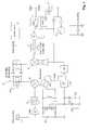
- FIG. 1shows a circuit diagram of an RF receiver
- FIG. 2part of the automatic gain control circuit
- FIG. 3part of the PLL circuit.
- a preferred embodiment of the inventionis an RF-receiver shown in FIG. 1 .
- the receiver shown hereis used for receiving the signal of GPS satellites at 1575.42 MHz, but the same technique can be applied to other type of radio receivers, in particular for digital signals.
- the receivercomprises an antenna 1 with low noise amplifier 2 and an input filter 3 .
- the signal from input filter 3is fed to a frequency mixer 4 , which mixes the carrier at 1575.42 MHz with a frequency of 1554.96 MHz to generate a downconverted first IF signal at 20.46 MHz.
- the first IF signalis filtered in a first IF filter 5 and fed to a second mixer 6 , where it is mixed with a frequency of 16.368 MHz to generate a second downconverted IF signal at 4.092 MHz.
- the second IF signalis fed through a second IF filter 7 and to a adjustable amplifier 8 .
- adjustable amplifier 9The output of adjustable amplifier 9 is fed to an A/D-converter 9 which generates a digital value of two bits SGN and MAG giving the sign and magnitude of the signal.
- the magnitude bitis analyzed by an adjustable gain control (AGC) 10 to set the gain of adjustable amplifier 8 .
- AGCadjustable gain control
- AGC 10The design of AGC 10 is shown in FIG. 2 . It comprises a switch control unit 20 controlling a switch 21 . In a first state, switch 21 connects a capacitor C 1 via a current source 22 to the positive supply voltage Vdd. In a second state, switch 21 connects capacitor C 1 via a current source 23 to the negative supply voltage or ground. In a thirds state, switch 23 is in high impedance state. The voltage U 1 over C 1 is fed as a control voltage to the high impedance input of a buffer 24 , the output of which controls amplifier 8 , wherein a lower voltage U 1 corresponds to a higher amplification in amplifier 8 .
- switch 21In normal operation, if MAG is 1, switch 21 is in its first state and, if MAG is 0, switch 21 is in its second state, i.e. the voltage over capacitor C 1 is proportional to the average value of MAG. If the average value of MAG is large, voltage U 1 increases, thereby decreasing the amplification of adjustable amplifier 8 and vice versa. The gain loop is adjusted such that it tries to hold MAG at an average value of 0.33, thereby holding the average signal strength at a desired value.
- the circuit of FIG. 1further comprises a Quartz oscillator 11 operating at 16.368 MHz. It generates the reference frequency for second mixer 6 . Furthermore, it provides a frequency base for a PLL.
- the PLLcomprises a phase and frequency comparator 12 for comparing the Quartz oscillator frequency divided by 16 to the PLL's frequency divided by 1520.
- the output of comparator 12is fed to a low pass filter comprising storage capacitors C 2 , C 3 , the voltage U 2 over which is the control voltage for the resonance frequency of a tank circuit 13 of a VCO 14 .
- the VCO's frequencyis kept at 1554.96 MHz, the reference frequency for first mixer 4 .
- FIG. 3The design of the part of the PLL that drives capacitors C 2 , C 3 is shown in FIG. 3 . It comprises a switch control unit 26 controlling a switch 27 . In a first state, switch 27 connects capacitors C 2 , C 3 via a current source 29 to the positive supply voltage Vdd. In a second state, switch 27 connects capacitors C 2 , C 3 via a current source 30 to the negative supply voltage or ground. In a third state, switch 27 is in high impedance state. If the comparator finds that the VCO's frequency is too low, switch 27 is primarily set to its first state, thereby increasing voltage U 2 over the capacitors, while, if the VCO's frequency is too high and for decreasing voltage U 2 , switch 27 is primarily in its second state.
- the circuit of FIG. 1comprises a control or power save unit 15 .
- the purpose of this power save unitis to temporarily switch off the circuits of the RF receiver for conservation of power.
- the position and length of the switch-off periodscan e.g. be selected according to a known temporal structure of the incoming signal or according to requirements of the user of the RF receiver.
- Power save unit 15switches off power supply to mixers 4 , 6 , amplifiers 2 , 8 , ADC 9 and AGC 10 , as well as to the PLL (comparator 12 , VCO 14 and frequency dividers) by issuing a control signal PWR SAVE.
- Typical power-off periodsmay e.g. have a duration between 1 ms and several seconds.
- the start-up time of the receiverwould be limited by the time it takes for the circuit to re-establish its dynamic settings. These settings are the amplification of adjustable amplifier 8 as well as the frequency of the PLL.
- the circuit of FIG. 1is designed to store these settings as control voltages U 1 , U 2 over the capacitors C 1 and C 2 or C 3 . While power is off, the load impedance offered by the circuits to these capacitors is high enough to make the discharge time of the capacitors much longer than a typical power-off period.
- a typical power-off periodis e.g. limited by a few seconds, while the discharge time is e.g. 100 times as large.
- capacitors C 1 , C 2 and C 3serve two purposes. First they act as low pass filters or integraters in their corresponding feed-back loops (ACG and PLL), second they store the setting of the loop during power-off.
- switches 21 and 27are both set to their third, high impedance state while the signal PWR SAVE indicates that the circuit is switched off.
- the capacities of the capacitorscan be increased where possible.
- active hold circuitscan be used to maintain the voltage of the capacitors during power-off periods.
- the storage capacitorcan e.g. be arranged in the negative feedback loop between the amplifier output and its inverting input.
- the LNA 2 , the frequency mixers 4 , 6 , the filters 5 , 7 , the amplifier 8 and the AGC 10form the analogue section of the receiver of FIG. 1 .
- the settings of this sectionare stored during power-off periods by saving the control voltages for the amplifier 8 and the VCO.
- the circuitBy storing the control voltages in the capacitors, the circuit can be switched back on quickly because its settings are maintained.
- the principle described herecan be used in other electronic circuits having settings that can be controlled by control voltages.
- the control voltagescan be stored in suitable capacitors while power is shut down.
- the technique shown hereis especially suited for PLL circuits in any application or for storing the amplification setting or setpoint of an adjustable RF or LF amplifier. It can also be used for storing the settings of any feedback loops.
- power save unit 15is controlled automatically, i.e. the time and duration of the switch-off periods are not directly determined by the user.
- power save unit 15could also be controlled by the user directly.
Landscapes
- Engineering & Computer Science (AREA)
- Computer Networks & Wireless Communication (AREA)
- Signal Processing (AREA)
- Radar, Positioning & Navigation (AREA)
- Remote Sensing (AREA)
- General Physics & Mathematics (AREA)
- Physics & Mathematics (AREA)
- Circuits Of Receivers In General (AREA)
- Stabilization Of Oscillater, Synchronisation, Frequency Synthesizers (AREA)
- Control Of Amplification And Gain Control (AREA)
- Selective Calling Equipment (AREA)
- Burglar Alarm Systems (AREA)
- Superheterodyne Receivers (AREA)
- Power Conversion In General (AREA)
Abstract
Description
Claims (23)
Applications Claiming Priority (2)
| Application Number | Priority Date | Filing Date | Title |
|---|---|---|---|
| EP00810933AEP1198068B1 (en) | 2000-10-10 | 2000-10-10 | Electronic circuit and RF receiver with power save control |
| EPEP-00810933.2 | 2000-10-10 |
Publications (2)
| Publication Number | Publication Date |
|---|---|
| US20020077074A1 US20020077074A1 (en) | 2002-06-20 |
| US6968220B2true US6968220B2 (en) | 2005-11-22 |
Family
ID=8174962
Family Applications (1)
| Application Number | Title | Priority Date | Filing Date |
|---|---|---|---|
| US09/973,593Expired - Fee RelatedUS6968220B2 (en) | 2000-10-10 | 2001-10-09 | RF receiver with power off control |
Country Status (6)
| Country | Link |
|---|---|
| US (1) | US6968220B2 (en) |
| EP (1) | EP1198068B1 (en) |
| JP (1) | JP3995440B2 (en) |
| AT (1) | ATE393496T1 (en) |
| CA (1) | CA2357499A1 (en) |
| DE (1) | DE60038679T2 (en) |
Cited By (5)
| Publication number | Priority date | Publication date | Assignee | Title |
|---|---|---|---|---|
| US20050176462A1 (en)* | 2004-02-06 | 2005-08-11 | Kenichi Kawasaki | Systems and methods for reducing power consumption in a receiver |
| US20050221790A1 (en)* | 2004-04-05 | 2005-10-06 | Persico Charles J | Power saving mode for receiver circuit blocks based on transmitter activity |
| US20090213912A1 (en)* | 2007-11-27 | 2009-08-27 | Nemerix Sa | Multipath mitigation gnss receiver |
| WO2008084474A3 (en)* | 2007-01-11 | 2010-02-04 | Audiodent Israel Ltd. | Low power radio frequency receiver |
| US20140184444A1 (en)* | 2012-12-28 | 2014-07-03 | Fujitsu Mobile Communications Limited | Communication device and switching method |
Families Citing this family (12)
| Publication number | Priority date | Publication date | Assignee | Title |
|---|---|---|---|---|
| FI113817B (en)* | 2002-05-27 | 2004-06-15 | Nokia Corp | Improved circuit arrangement for a phase lock, integrated circuit with a phase lock, method utilizing a phase lock and terminal in a cellular network |
| US7184799B1 (en)* | 2003-05-14 | 2007-02-27 | Marvell International Ltd. | Method and apparatus for reducing wake up time of a powered down device |
| US7724846B2 (en)* | 2003-06-05 | 2010-05-25 | Broadcom Corporation | Method and apparatus for mitigating interference in a satellite signal receiver |
| US7551132B2 (en)* | 2004-07-02 | 2009-06-23 | Nemerix Sa | GPS receiver with fast acquisition time |
| ATE521904T1 (en) | 2003-07-03 | 2011-09-15 | Qualcomm Inc | GPS RECEIVER WITH SHORT DETECTION TIME |
| JP4658050B2 (en)* | 2003-09-02 | 2011-03-23 | サーフ テクノロジー インコーポレイテッド | Signal processing system for satellite positioning signals |
| US7962362B2 (en)* | 2004-08-11 | 2011-06-14 | Canadian Bank Note Company, Limited | Promoting customer loyalty |
| US7522898B2 (en)* | 2005-06-01 | 2009-04-21 | Wilinx Corporation | High frequency synthesizer circuits and methods |
| WO2007068661A1 (en) | 2005-12-16 | 2007-06-21 | Nemerix Sa | Signal processor and signal processing method |
| US9151846B2 (en) | 2005-12-16 | 2015-10-06 | Qualcomm Incorporated | Signal processor and signal processing method |
| EP1903346A1 (en) | 2006-09-21 | 2008-03-26 | Nemerix SA | Memory reduction in GNSS receiver |
| EP1916535B1 (en) | 2006-10-26 | 2015-11-18 | Qualcomm Incorporated | GNSS receiver with cross-correlation rejection |
Citations (18)
| Publication number | Priority date | Publication date | Assignee | Title |
|---|---|---|---|---|
| US4011514A (en)* | 1974-05-06 | 1977-03-08 | Unitech Przedsiebiorstwo Techniczno-Hand-Lowe | Memory circuit for tuning of an electronically tuned receiver to a preselected station |
| US4340973A (en)* | 1979-09-29 | 1982-07-20 | Nippon Electric Co., Ltd. | Selective calling receiver including a voltage converter with low power consumption |
| US4380832A (en) | 1980-07-31 | 1983-04-19 | Nippon Electric Co., Ltd. | Portable radio communication device having signal processing circuit with presetting function |
| US4511923A (en)* | 1980-11-14 | 1985-04-16 | Texas Instruments Incorporated | Method for tuning the input stage of a receiver to a desired receiving frequency and circuit arrangement for carrying out the method |
| US4590611A (en)* | 1983-02-04 | 1986-05-20 | Deutsche Thomson-Brandt Gmbh | Tuner for communications equipment |
| US4631737A (en) | 1984-12-06 | 1986-12-23 | Motorola, Inc. | Self biasing direct coupled data limiter |
| US4866261A (en) | 1987-01-02 | 1989-09-12 | Motorola, Inc. | Data limiter having current controlled response time |
| US4893094A (en)* | 1989-03-13 | 1990-01-09 | Motorola, Inc. | Frequency synthesizer with control of start-up battery saving operations |
| US4929851A (en) | 1989-01-23 | 1990-05-29 | Motorola, Inc. | Data limiter for a radio pager |
| US4956711A (en)* | 1983-12-27 | 1990-09-11 | Deutsche Thompson-Brandt Gmbh | Automatic balancing system for communications receiver apparatus |
| US5128632A (en)* | 1991-05-16 | 1992-07-07 | Motorola, Inc. | Adaptive lock time controller for a frequency synthesizer and method therefor |
| US5201063A (en)* | 1988-12-28 | 1993-04-06 | Astec International Ltd. | Setting of electronic circuits in a radio telephone |
| US5448756A (en)* | 1992-07-02 | 1995-09-05 | Motorola, Inc. | High frequency battery saver for a radio receiver |
| US6223061B1 (en)* | 1997-07-25 | 2001-04-24 | Cleveland Medical Devices Inc. | Apparatus for low power radio communications |
| US6463050B1 (en)* | 1997-10-28 | 2002-10-08 | Nec Corporation | Power saving method and apparatus for radio base station |
| US6532357B1 (en)* | 1998-08-07 | 2003-03-11 | Matsushita Electric Industrial Co., Ltd. | Radio communication device and transmission power control method for radio communication device |
| US6658240B1 (en)* | 1998-08-17 | 2003-12-02 | Telefonaktiebolaget Lm Ericsson | Multiband frequency generation device and related method |
| US6697436B1 (en)* | 1999-07-13 | 2004-02-24 | Pmc-Sierra, Inc. | Transmission antenna array system with predistortion |
Family Cites Families (2)
| Publication number | Priority date | Publication date | Assignee | Title |
|---|---|---|---|---|
| US4521918A (en)* | 1980-11-10 | 1985-06-04 | General Electric Company | Battery saving frequency synthesizer arrangement |
| CH677298A5 (en)* | 1989-04-17 | 1991-04-30 | Koechler Erika Fa | Frequency synthesiser circuit for portable radio receiver - has switch interrupting voltage to frequency divider and phase detector for reduced battery requirement |
- 2000
- 2000-10-10ATAT00810933Tpatent/ATE393496T1/ennot_activeIP Right Cessation
- 2000-10-10DEDE60038679Tpatent/DE60038679T2/ennot_activeExpired - Lifetime
- 2000-10-10EPEP00810933Apatent/EP1198068B1/ennot_activeExpired - Lifetime
- 2001
- 2001-09-19CACA002357499Apatent/CA2357499A1/ennot_activeAbandoned
- 2001-10-09USUS09/973,593patent/US6968220B2/ennot_activeExpired - Fee Related
- 2001-10-09JPJP2001311180Apatent/JP3995440B2/ennot_activeExpired - Fee Related
Patent Citations (18)
| Publication number | Priority date | Publication date | Assignee | Title |
|---|---|---|---|---|
| US4011514A (en)* | 1974-05-06 | 1977-03-08 | Unitech Przedsiebiorstwo Techniczno-Hand-Lowe | Memory circuit for tuning of an electronically tuned receiver to a preselected station |
| US4340973A (en)* | 1979-09-29 | 1982-07-20 | Nippon Electric Co., Ltd. | Selective calling receiver including a voltage converter with low power consumption |
| US4380832A (en) | 1980-07-31 | 1983-04-19 | Nippon Electric Co., Ltd. | Portable radio communication device having signal processing circuit with presetting function |
| US4511923A (en)* | 1980-11-14 | 1985-04-16 | Texas Instruments Incorporated | Method for tuning the input stage of a receiver to a desired receiving frequency and circuit arrangement for carrying out the method |
| US4590611A (en)* | 1983-02-04 | 1986-05-20 | Deutsche Thomson-Brandt Gmbh | Tuner for communications equipment |
| US4956711A (en)* | 1983-12-27 | 1990-09-11 | Deutsche Thompson-Brandt Gmbh | Automatic balancing system for communications receiver apparatus |
| US4631737A (en) | 1984-12-06 | 1986-12-23 | Motorola, Inc. | Self biasing direct coupled data limiter |
| US4866261A (en) | 1987-01-02 | 1989-09-12 | Motorola, Inc. | Data limiter having current controlled response time |
| US5201063A (en)* | 1988-12-28 | 1993-04-06 | Astec International Ltd. | Setting of electronic circuits in a radio telephone |
| US4929851A (en) | 1989-01-23 | 1990-05-29 | Motorola, Inc. | Data limiter for a radio pager |
| US4893094A (en)* | 1989-03-13 | 1990-01-09 | Motorola, Inc. | Frequency synthesizer with control of start-up battery saving operations |
| US5128632A (en)* | 1991-05-16 | 1992-07-07 | Motorola, Inc. | Adaptive lock time controller for a frequency synthesizer and method therefor |
| US5448756A (en)* | 1992-07-02 | 1995-09-05 | Motorola, Inc. | High frequency battery saver for a radio receiver |
| US6223061B1 (en)* | 1997-07-25 | 2001-04-24 | Cleveland Medical Devices Inc. | Apparatus for low power radio communications |
| US6463050B1 (en)* | 1997-10-28 | 2002-10-08 | Nec Corporation | Power saving method and apparatus for radio base station |
| US6532357B1 (en)* | 1998-08-07 | 2003-03-11 | Matsushita Electric Industrial Co., Ltd. | Radio communication device and transmission power control method for radio communication device |
| US6658240B1 (en)* | 1998-08-17 | 2003-12-02 | Telefonaktiebolaget Lm Ericsson | Multiband frequency generation device and related method |
| US6697436B1 (en)* | 1999-07-13 | 2004-02-24 | Pmc-Sierra, Inc. | Transmission antenna array system with predistortion |
Cited By (6)
| Publication number | Priority date | Publication date | Assignee | Title |
|---|---|---|---|---|
| US20050176462A1 (en)* | 2004-02-06 | 2005-08-11 | Kenichi Kawasaki | Systems and methods for reducing power consumption in a receiver |
| US20050221790A1 (en)* | 2004-04-05 | 2005-10-06 | Persico Charles J | Power saving mode for receiver circuit blocks based on transmitter activity |
| US7283851B2 (en)* | 2004-04-05 | 2007-10-16 | Qualcomm Incorporated | Power saving mode for receiver circuit blocks based on transmitter activity |
| WO2008084474A3 (en)* | 2007-01-11 | 2010-02-04 | Audiodent Israel Ltd. | Low power radio frequency receiver |
| US20090213912A1 (en)* | 2007-11-27 | 2009-08-27 | Nemerix Sa | Multipath mitigation gnss receiver |
| US20140184444A1 (en)* | 2012-12-28 | 2014-07-03 | Fujitsu Mobile Communications Limited | Communication device and switching method |
Also Published As
| Publication number | Publication date |
|---|---|
| CA2357499A1 (en) | 2002-04-10 |
| DE60038679T2 (en) | 2009-05-07 |
| EP1198068B1 (en) | 2008-04-23 |
| ATE393496T1 (en) | 2008-05-15 |
| JP3995440B2 (en) | 2007-10-24 |
| EP1198068A1 (en) | 2002-04-17 |
| DE60038679D1 (en) | 2008-06-05 |
| JP2002185347A (en) | 2002-06-28 |
| US20020077074A1 (en) | 2002-06-20 |
Similar Documents
| Publication | Publication Date | Title |
|---|---|---|
| US6968220B2 (en) | RF receiver with power off control | |
| US8036619B2 (en) | Oscillator having controllable bias modes and power consumption | |
| US6741127B2 (en) | High-frequency amplifier circuit and radio communication apparatus using same | |
| US6963736B2 (en) | Method for receiving a radio frequency (RF) signal and RF receiver | |
| US20100056097A1 (en) | Low power radio frequency receiver | |
| US8781539B1 (en) | Method and apparatus for reducing wake up time of a powered down device | |
| US6788161B2 (en) | Integrated oscillator circuit that inhibits noise generated by biasing circuitry | |
| US20120142283A1 (en) | Wireless communication apparatus | |
| US6757028B2 (en) | Television tuner for reducing power consumption and video device using the television tuner | |
| US20020079977A1 (en) | Oscillator and communication apparatus using the same | |
| US9112508B2 (en) | Adaptive powered local oscillator generator circuit and related method | |
| JP2001036349A (en) | Pll detecting circuit | |
| JPH05167465A (en) | Receiver | |
| US5939911A (en) | Frequency prescaler method and apparatus responsive to low input drive levels | |
| US5483687A (en) | Operational transconductance amplifier track and hold system | |
| KR100575985B1 (en) | Sleep Mode Control Device and Method for Direct Conversion in Wireless Communication System | |
| JP2866843B1 (en) | FHSS wireless LAN transceiver | |
| JP2657137B2 (en) | Control unit for radio receiving circuit | |
| US20140155009A1 (en) | Crystal control scheme to improve performance of a receiver | |
| JP3504847B2 (en) | DBS tuner for satellite broadcasting reception | |
| JPH08125561A (en) | Tuner | |
| JP2004274420A (en) | Front end for broadcast reception | |
| JP2000349662A (en) | Radio communication unit | |
| JP2005033352A (en) | Transmitting circuit | |
| JP2004350029A (en) | Broadcast receiver |
Legal Events
| Date | Code | Title | Description |
|---|---|---|---|
| AS | Assignment | Owner name:T CHIP SEMICONDUCTOR SA, SWITZERLAND Free format text:ASSIGNMENT OF ASSIGNORS INTEREST;ASSIGNOR:PIAZZA, FRANCESCO;REEL/FRAME:012642/0155 Effective date:20011128 | |
| AS | Assignment | Owner name:NEMERIX SA, SWITZERLAND Free format text:AUCTION;ASSIGNOR:T CHIP SEMICONDUCTOR SA;REEL/FRAME:015474/0129 Effective date:20021219 | |
| CC | Certificate of correction | ||
| FEPP | Fee payment procedure | Free format text:PAYOR NUMBER ASSIGNED (ORIGINAL EVENT CODE: ASPN); ENTITY STATUS OF PATENT OWNER: LARGE ENTITY | |
| FEPP | Fee payment procedure | Free format text:PAYER NUMBER DE-ASSIGNED (ORIGINAL EVENT CODE: RMPN); ENTITY STATUS OF PATENT OWNER: LARGE ENTITY Free format text:PAYOR NUMBER ASSIGNED (ORIGINAL EVENT CODE: ASPN); ENTITY STATUS OF PATENT OWNER: LARGE ENTITY | |
| FPAY | Fee payment | Year of fee payment:4 | |
| AS | Assignment | Owner name:QUALCOMM INCORPORATED, CALIFORNIA Free format text:ASSIGNMENT OF ASSIGNORS INTEREST;ASSIGNOR:NEMERIX, SA;REEL/FRAME:022746/0424 Effective date:20090430 Owner name:QUALCOMM INCORPORATED,CALIFORNIA Free format text:ASSIGNMENT OF ASSIGNORS INTEREST;ASSIGNOR:NEMERIX, SA;REEL/FRAME:022746/0424 Effective date:20090430 | |
| FPAY | Fee payment | Year of fee payment:8 | |
| REMI | Maintenance fee reminder mailed | ||
| LAPS | Lapse for failure to pay maintenance fees | Free format text:PATENT EXPIRED FOR FAILURE TO PAY MAINTENANCE FEES (ORIGINAL EVENT CODE: EXP.) | |
| STCH | Information on status: patent discontinuation | Free format text:PATENT EXPIRED DUE TO NONPAYMENT OF MAINTENANCE FEES UNDER 37 CFR 1.362 | |
| FP | Lapsed due to failure to pay maintenance fee | Effective date:20171122 |