US6967885B2 - Concurrent refresh mode with distributed row address counters in an embedded DRAM - Google Patents
Concurrent refresh mode with distributed row address counters in an embedded DRAMDownload PDFInfo
- Publication number
- US6967885B2 US6967885B2US10/757,846US75784604AUS6967885B2US 6967885 B2US6967885 B2US 6967885B2US 75784604 AUS75784604 AUS 75784604AUS 6967885 B2US6967885 B2US 6967885B2
- Authority
- US
- United States
- Prior art keywords
- memory
- refresh
- array
- memory array
- word address
- Prior art date
- Legal status (The legal status is an assumption and is not a legal conclusion. Google has not performed a legal analysis and makes no representation as to the accuracy of the status listed.)
- Expired - Lifetime
Links
- 230000015654memoryEffects0.000claimsabstractdescription178
- 238000003491arrayMethods0.000claimsabstractdescription29
- 239000004065semiconductorSubstances0.000claimsdescription23
- 230000008878couplingEffects0.000claimsdescription7
- 238000010168coupling processMethods0.000claimsdescription7
- 238000005859coupling reactionMethods0.000claimsdescription7
- 230000003213activating effectEffects0.000claimsdescription6
- 239000011159matrix materialSubstances0.000claimsdescription6
- 230000000977initiatory effectEffects0.000claims1
- 230000037431insertionEffects0.000abstract1
- 238000003780insertionMethods0.000abstract1
- 238000013461designMethods0.000description9
- 230000006870functionEffects0.000description9
- 230000014759maintenance of locationEffects0.000description8
- 238000000034methodMethods0.000description7
- 238000013459approachMethods0.000description5
- 230000004913activationEffects0.000description3
- 230000004048modificationEffects0.000description3
- 238000012986modificationMethods0.000description3
- 238000011161developmentMethods0.000description2
- 230000009977dual effectEffects0.000description2
- 238000005516engineering processMethods0.000description2
- 230000006872improvementEffects0.000description2
- 238000013507mappingMethods0.000description2
- 208000032750Device leakageDiseases0.000description1
- 230000008901benefitEffects0.000description1
- 238000004891communicationMethods0.000description1
- 238000007796conventional methodMethods0.000description1
- 238000010586diagramMethods0.000description1
- 230000008569processEffects0.000description1
- 230000009467reductionEffects0.000description1
- 239000000849selective androgen receptor modulatorSubstances0.000description1
- 230000003068static effectEffects0.000description1
- 238000012546transferMethods0.000description1
- 230000007704transitionEffects0.000description1
Images


Classifications
- G—PHYSICS
- G11—INFORMATION STORAGE
- G11C—STATIC STORES
- G11C11/00—Digital stores characterised by the use of particular electric or magnetic storage elements; Storage elements therefor
- G11C11/21—Digital stores characterised by the use of particular electric or magnetic storage elements; Storage elements therefor using electric elements
- G11C11/34—Digital stores characterised by the use of particular electric or magnetic storage elements; Storage elements therefor using electric elements using semiconductor devices
- G11C11/40—Digital stores characterised by the use of particular electric or magnetic storage elements; Storage elements therefor using electric elements using semiconductor devices using transistors
- G11C11/401—Digital stores characterised by the use of particular electric or magnetic storage elements; Storage elements therefor using electric elements using semiconductor devices using transistors forming cells needing refreshing or charge regeneration, i.e. dynamic cells
- G11C11/406—Management or control of the refreshing or charge-regeneration cycles
- G11C11/40618—Refresh operations over multiple banks or interleaving
- G—PHYSICS
- G11—INFORMATION STORAGE
- G11C—STATIC STORES
- G11C11/00—Digital stores characterised by the use of particular electric or magnetic storage elements; Storage elements therefor
- G11C11/21—Digital stores characterised by the use of particular electric or magnetic storage elements; Storage elements therefor using electric elements
- G11C11/34—Digital stores characterised by the use of particular electric or magnetic storage elements; Storage elements therefor using electric elements using semiconductor devices
- G11C11/40—Digital stores characterised by the use of particular electric or magnetic storage elements; Storage elements therefor using electric elements using semiconductor devices using transistors
- G11C11/401—Digital stores characterised by the use of particular electric or magnetic storage elements; Storage elements therefor using electric elements using semiconductor devices using transistors forming cells needing refreshing or charge regeneration, i.e. dynamic cells
- G11C11/406—Management or control of the refreshing or charge-regeneration cycles
- G—PHYSICS
- G11—INFORMATION STORAGE
- G11C—STATIC STORES
- G11C2207/00—Indexing scheme relating to arrangements for writing information into, or reading information out from, a digital store
- G11C2207/10—Aspects relating to interfaces of memory device to external buses
- G11C2207/104—Embedded memory devices, e.g. memories with a processing device on the same die or ASIC memory designs
Definitions
- This inventionis generally related to an embedded dynamic random access memory (embedded DRAM), and more particularly, to a concurrent refresh mode and design which employs distributed row address counters integrated in each DRAM.
- embedded DRAMembedded dynamic random access memory
- Improvements in semiconductor technologyhave enabled the design of processors having performance exceeding 1 Giga Hz.
- the system performanceis often constrained by the performance of its memory.
- the presence of this drawbackhas created a potentially strong demand for high performance embedded DRAMs to help the processor achieve the necessary speed.
- FIG. 1there are shown simulated sensing signals illustrating the aforementioned assertions.
- a conventional array device 52 A(not shown) having a 2.5 V wordline boosted voltage (VPP) and supported by a long bitline coupling 256 cells (256 b/BL) is compared to the plot referenced (B), wherein a logic array device 22 A (not shown) powered by a 1.5V VPP is supported by a short bitline coupled to 64 cells.
- the sensing signalis extracted by changing the signal development time (tSIG), i.e., the time to develop a signal on the bitline when a wordline is activated over a random access cycle time (tRC) in a grounded sensing scheme.
- tSIGsignal development time
- tRCrandom access cycle time
- the logic array device 22 Ais enabled by approximately 30% more current than that applicable to the corresponding array device 52 A, approximately 80 mV of the sensing voltage can be achieved even for a 3.2 ns random access cycle time.
- employing a logic array device 22 Arequires a reduction in the data retention time to a value as small as 64 ⁇ s. The shorter retention time greatly reduces the memory availability, particularly for a large density memory because all the memory cells need to be refreshed within a given retention time to maintain the data bits.
- a 4 Mb memory having 8K wordlinesrequires 8K refresh cycles within 64 ⁇ s. This, in turn, requires at least one refresh command every 8 ns, resulting in the memory being unavailable for an 8 ns random cycle memory.
- a concurrent refresh modeis typically used, as described, e.g., in U.S. Pat. No. 4,185,323 issued to Johnson et al.
- FIG. 2is a block representation of a semiconductor memory chip 200 consisting of a plurality of DRAM memory banks 210 .
- Each memory bank 210consists of a plurality of DRAM memory cells (not shown) arranged in a two-dimensional matrix configuration, well known in the art, and which, accordingly, will not be discussed further.
- a memory access operationread, write, or refresh operation
- the DRAM banke.g., 210 i
- the DRAM bankbecomes unavailable for a random access cycle time tRC.
- other DRAM bankse.g., 210 j
- the memory availabilitygreatly improves by concurrently performing a refresh operation while enabling a memory access operation.
- There are two known methods for enabling a concurrent refresh mode in a semiconductor memorythe details of which will be discussed hereinafter, as explained hereinafter with reference to FIGS. 3 and 4 .
- FIG. 3illustrates a first method to enable a concurrent refresh mode in a conventional static random access memory (SRAM) buffer. Details of this approach are described, e.g., in U.S. Pat. No. 5,999,474, issued to Leung et al.
- Semiconductor memory chip 300consists of a plurality of DRAM banks ( 310 DRAM), each consisting of a plurality of memory cells arranged in a two dimensional array configuration. Accessing bank 310 DRAM- 310 j while concurrently refreshing at least one other bank 310 DRAM- 310 k is possible as long as the accessed bank and the refreshed bank differ from one another.
- SRAMstatic random access memory
- memory chip 300is enhanced by adding an SRAM bank ( 310 SRAM), featuring a dual port function that allows receiving and transferring data within a clock cycle.
- the access operation of the DRAM banks ( 310 DRAM) and SLAM ( 310 SRAM)are controlled by the TAG memory ( 310 TAG), while the memory access of the memory chip 300 is enabled by a read or write command (not shown), a bank address (XBADD), and a word address (XWADD), wherein XBADD and XWADD identify one of the DRAM banks ( 310 DRAM) and the appropriate wordline within the selected DRAM banks.
- wordline ( 320 TAG) in the TAG memory ( 310 TAG) and the wordlines ( 320 s ) in SRAM bank ( 310 SRAM)are activated by decoding the word address (XWADD).
- XWADDword address
- Thisenables reading out data in the memory cells ( 330 TAG) in within the TAG memory ( 310 TAG) and data in the memory cells ( 330 s ) within the SRAM buffer ( 310 SRAM).
- the read data bits ( 330 TAG) of the TAG memory ( 310 TAG)defines the bank address (TBADD) which, in turn, identifies the corresponding DRAM bank for the data bits ( 330 s ) currently read from the SRAM buffer ( 310 SRAM).
- the data bits ( 330 s )are the ones that are requested by the memory access command, since the data bits ( 330 s ) were previously copied from the corresponding DRAM bank to the SRAM buffer ( 310 SRAM). Therefore, no DRAM bank access is necessary, and the read data bits from the SRAM buffer ( 310 SRAM) are read am from the XDATA pins.
- the TAG memory ( 310 TAG)control the DRAM banks ( 310 DRAM) as follows.
- the data bits ( 330 s ) in the SRAM buffer ( 310 SRAM)are stored back in DRAM bank ( 310 i ), where the wordline 320 i is same as the wordline address of 320 s (Direct Mapping). This allows data bits to be transferred from the SRAM memory cells ( 330 s ) to the DRAM memory cells ( 330 i ). Concurrent with the bank address input (XBADD), the corresponding DRAM bank ( 310 j ) is activated for a read operation.
- the cell's data bits ( 330 j ) in the corresponding DRAM bank ( 310 j )are read out, where wordline 320 j coincides with the wordline address of 320 s (Direct Mapping). They are read am from the XDATA pins.
- the cell's data bits ( 330 j )are also stored in the cells ( 330 s ) of the SRAM buffer ( 310 SRAM) TBADD is therefore updated to identify the DRAM bank 310 j for a future memory access command.
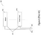
- FIG. 4illustrates the second method that enables a simultaneous refresh by utilizing a concurrent function for the DRAM.
- Semiconductor memory chip 400consists of a plurality of DRAM banks 410 ( 410 i through 410 j ), each of which is controlled by the corresponding address and command ports ( 420 i through 420 j ). Therefore, any two or more banks can be activated concurrently.
- memory bank 410 iremains in the read mode while still enabling a refresh operation for memory bank 410 j .
- this approachrequires a complex refresh system management to avoid a bank access contention caused by the concurrent function.
- This inventiondescribes a concurrent refresh mode, wherein the embedded DRAM enables a simultaneous memory access and refreshes the operations by way of a simple system modification.
- the concurrent refresh modeis realized by allowing the unselected memory array to be refreshed only by a refresh bank select port.
- macro row address counters integrated in each banktrack the wordline address within the corresponding banks. This greatly reduces the complexity of managing the refresh address in a concurrent refresh mode, since the in-macro refresh counter in each bank maintains independently the wordline refreshed.
- the system improvement that employs this concurrent refresh methodis achieved solely by managing the bank access contention.
- the present inventionis particularly advantageous for a multi-bank system having a short retention DRAM, since the refresh management can be integrated within the existing multi-bank management system. As long as the bank contention is managed, 100% of memory availability can be realized.
- a semiconductor memoryconsisting of two or more memory arrays, wherein each of the two arrays is coupled to a row address counter to generate a first word address within each array when a refresh command is given, while enabling at least one more array to be in a memory access mode.
- a semiconductor memorythat includes: i) a plurality of memory arrays, each of which comprises a plurality of memory cells arranged in a matrix and controlled by a row address counter uniquely assigned to each of the memory arrays, the row address counter generating a first word address; and ii) means for enabling a refresh operation in the memory cells, the memory cells being identified by the first word address when a refresh command is issued to a corresponding memory array.
- FIG. 1shows two plots representing simulated sensing signals generated from two 256 b/BL and 64 b/BL DRAM arrays that illustrate the conventional shift from a data retention driven design to a memory availability driven design.
- FIG. 2shows a block diagram representing a multi-bank DRAM memory device to illustrate how the memory availability improves by applying a prior art concurrent performance of a refresh operation while enabling the memory access.
- FIG. 3illustrates a prior art method to enable a concurrent refresh mode in memory chip 300 which has been is enhanced by adding an SRAM, and which features a dual port function to receive and transfer data within one clock cycle.
- FIG. 4is shows another conventional method that enables a concurrent refresh mode by utilizing a simultaneous function for a DRAM, wherein by way of the simultaneous function, the memory bank remains in the read mode while still enabling a refresh operation for the memory bank.
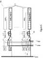
- FIG. 5illustrates a memory architecture applicable to a concurrent refresh mode with distributed row address counters, in accordance with the present invention.
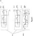
- FIG. 6shows a transistor level schematic of the row address counter integrated in each bank of the DRAM, according to present invention.
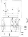
- FIG. 7shows a detailed bank architecture, consisting of a core, row address and switching elements, according to present invention.
- FIG. 5there is shown a memory architecture provided with the inventive concurrent refresh mode with distributed row address counters.
- the present embodimentassumes an embedded DRAM macro.
- the inventionis also applicable to a stand-alone DRAM.
- the DRAM macroemploys a flexible multi-bank protocol having 16 independent bank select ports BSEL 0-15 , each controlling a corresponding array of BANK 0-15 .
- BSEL 0-15may be implemented as a four bit bank address vector that identifies one array of BANK 0-15 .
- itfurther includes 16 refresh bank select ports RBSEL 0-15 , each controlling the corresponding array as a bank independently from the memory access operation.
- the basic concept of the present inventionis not a concurrent refresh mode, but the introduction of distributed row address counters integrated in each bank to achieve a greater simplification of the refresh management at the system level.
- Each arrayincludes a row address counter RAC (e.g., 520 ) that identifies the word address WRAC 0-6 for a concurrent refresh mode.
- Each arrayfurther includes a switch 530 to selectively couple either the word address WADD 0-6 or the word address WRAC 0-6 to the row decoder (not shown) of the array bank (BANK).
- the word address WADD 0-6 issued by bank select signal BSELis coupled to the row decoder (not shown) in array 510 via switch 530 . This allows the corresponding wordline (not shown) in the array 510 to be activated according to the word address WADD 0-6 .
- the word address (WRAC 0-6 ) from counter RAC 520is coupled to the row decoder (not shown) in the array by way of switch 530 .
- BSELi.e., BSEL 0
- RBESLi.e., RBSEL 0
- a memory access of an arrayi.e., BANK 0
- the wordline activation within the selected refresh banki.e. BANK 0
- avoiding a bank contentionis a well known design practice for a multi-bank memory system. Assuming that each array consists of 128 wordlines, data will be maintained as long as 128 refresh commands are issued for each bank within the retention time. This results in an almost total memory utilization by properly managing RBSEL.
- the bankmay be activated in a staggered manner for each bank-to-bank access time cycle (tRRD), while concurrently refreshing other arrays for each tRRD. Access contention between the accessed bank and the refreshed bank can be avoided as long as the activation of the same bank is longer than the random access cycle time (tRC).
- activating a subsequent bankeither by BSELn and RBSELn must be longer than tRC.
- This managementis much simpler than the existing concurrent refresh management with corresponding address and command ports.
- No refresh address management for the selected refresh bankis necessary.
- two or more memory arraysmay be simultaneously refreshed while enabling the memory access for each clock cycle. This is advantageously realized by simultaneously activating a plurality of the refresh bank control signals RBSEL 0-15 .
- the distributed RAC counter approachrequires controlling RBSEL for the corresponding refreshed bank without establishing communication between the address port and the respective control circuitry. This results in a current saving as large as 10 mA assuming a seven address bus transition, each having a 1.5 pF capacitance operating at 1 GHz frequency.
- the current saving advantageis further improved as the memory speed and density increase.
- FIG. 6is a transistor level schematic of the row address counter 520 integrated in each bank (BANK).
- the row address counterincludes seven counter logic elements, 610 — 0 to 610 — 6 , each generating a corresponding address bits WRAC 0-6 .
- Each counter logic elemente.g., 610 — 0
- Each counter logic elementconsists of two CMOS pass gates 622 and 624 , two CMOS latches 626 and 628 , and two inverters 620 and 630 .
- the refresh enable signal RBSEL shown in FIG. 5is coupled to the NMOS gate for CMOS pass gate 622 , and PMOS gate for CMOS pass gate 624 .
- RBSELis inverted by inverter 620 and coupled to the PMOS gate of CMOS pass gate 622 and NMOS gate of CMOS pass gate 624 . Therefore, as long as signal RBSEL is at low, CMOS pass gate 624 couples node N 2 to node N 3 , and subsequently to node N 4 . CMOS pass gate 622 remains off, isolating node N 0 from N 4 . The output of WRAC 0 (coupling to N 4 ) from the counter logic element 610 — 0 therefore follows node N 1 . When the signal RBSEL switches to high to enable a concurrent refresh mode, CMOS pass gates 622 and 624 switch on and off, respectively.
- WRAC 0maintains the state at the original value set by CMOS latch 628 .
- the state of node N 1is flipped by coupling node N 0 to node N 1 , (Note: because node N 0 is in the inverted state from WRAC 0 ).
- CMOS pass gates 622 and 624turn off and on, respectively, allowing bit WRAC 0 to flip and follow node N 1 , which has been already updated.
- the bit WRAC 0is flipped at each RBSEL cycle, and acts as the least significant address bit of the row address counter 520 .
- CMOS pass gate 622 in element 610 — nis coupled to the counter output N 4 in the element 610 — n ⁇ 1, where n is an integer from 1 to 6. This allows bits WRAC 1 . . . , WRAC 6 to flip over, respectively, every 2, 4, 8, 16, 32, and 64 RBSEL cycles, creating a seven bit counter to generate a refresh address within each array.
- FIG. 7shows a more detailed bank architecture consisting of array 510 , row address counter (RAC 520 ), and seven bit switching elements 530 .
- the arrayincludes a plurality of memory cells 715 arranged in a two-dimensional matrix as a cell array.
- the cell arrayis supported by row decoders 720 and bitline sense amplifiers 725 .
- the word address for a concurrent refresh mode and a memory access modeare supported by the word address WRAC 0 , . . . , WRAC 6 and the word address WADD 0 , . . . , WADD 6 , respectively.
- the selectionis realized by the seven switching elements 530 , each coupling either WADD or WRAC to the row decoder 720 .
- the bank select signal BSELswitches to high, activating the NMOS 732 in each switching element 530 .
- the WADD bitremains even after BSEL is switched to low by CMOS latch 736 .
- the refresh bank select signal RBSELswitches to high, activating NMOS 734 in each switching element 730 .
- Latching the word address in switching element 530allows the word address WADD 0 , . . . , WADD 6 to activate other banks during a multi-bank operation without waiting for the completion of the corresponding bank operation.
- a concurrent refresh operationmay be issued for each bank activation cycle.
- the first and second arraysare activated for refresh and memory access operations. Then, without waiting for the completion of the first and second memory array operation, the memory access operation for the third bank is enabled, while concurrently issuing the refresh operation for the forth array.
- the wordline WLis activated by row decoder 720 .
- the decoding bitsare determined by the address bits transferred from the seven bit switching elements 530 , as previously discussed.
- the wordlineswitches to high, the data bits in the cells 715 are read and written through bitline BL.
- Differential BL pairsare advantageously coupled to bitline sense amplifiers 725 , amplifying the small signal read from the cells 715 .
- the sense amplifiersare used for writing back the data bits to the cells ( 715 ), which is well know and which, therefore, will not be discussed.
Landscapes
- Engineering & Computer Science (AREA)
- Microelectronics & Electronic Packaging (AREA)
- Computer Hardware Design (AREA)
- Dram (AREA)
Abstract
Description
Claims (16)
Priority Applications (4)
| Application Number | Priority Date | Filing Date | Title |
|---|---|---|---|
| US10/757,846US6967885B2 (en) | 2004-01-15 | 2004-01-15 | Concurrent refresh mode with distributed row address counters in an embedded DRAM |
| TW094100085ATWI330368B (en) | 2004-01-15 | 2005-01-03 | An embedded dram performing concurrent refresh mode with distributed row address counters |
| JP2005007728AJP4524194B2 (en) | 2004-01-15 | 2005-01-14 | Simultaneous refresh mode with distributed row address counter in embedded DRAM |
| CNB200510002155XACN100485806C (en) | 2004-01-15 | 2005-01-14 | Concurrent refresh mode embedded DRAM with distributed row address counters |
Applications Claiming Priority (1)
| Application Number | Priority Date | Filing Date | Title |
|---|---|---|---|
| US10/757,846US6967885B2 (en) | 2004-01-15 | 2004-01-15 | Concurrent refresh mode with distributed row address counters in an embedded DRAM |
Publications (2)
| Publication Number | Publication Date |
|---|---|
| US20050157577A1 US20050157577A1 (en) | 2005-07-21 |
| US6967885B2true US6967885B2 (en) | 2005-11-22 |
Family
ID=34749423
Family Applications (1)
| Application Number | Title | Priority Date | Filing Date |
|---|---|---|---|
| US10/757,846Expired - LifetimeUS6967885B2 (en) | 2004-01-15 | 2004-01-15 | Concurrent refresh mode with distributed row address counters in an embedded DRAM |
Country Status (4)
| Country | Link |
|---|---|
| US (1) | US6967885B2 (en) |
| JP (1) | JP4524194B2 (en) |
| CN (1) | CN100485806C (en) |
| TW (1) | TWI330368B (en) |
Cited By (18)
| Publication number | Priority date | Publication date | Assignee | Title |
|---|---|---|---|---|
| US20050162960A1 (en)* | 2004-01-28 | 2005-07-28 | Nec Electronics Corporation | Semiconductor integrated circuit device |
| US20060044912A1 (en)* | 2004-08-31 | 2006-03-02 | Byoung-Sul Kim | Method and apparatus for refreshing memory device |
| US20070086258A1 (en)* | 2005-10-17 | 2007-04-19 | Freebern Margaret C | Directed auto-refresh for a dynamic random access memory |
| US20070211549A1 (en)* | 2006-03-09 | 2007-09-13 | Fujitsu Limited | Semiconductor memory, memory system, and operation method of semiconductor memory |
| US20070230264A1 (en)* | 2006-03-30 | 2007-10-04 | Fujitsu Limited | Dynamic semiconductor memory reducing the frequency of occurrence of refresh command request and refresh control method thereof |
| US20080253212A1 (en)* | 2007-04-10 | 2008-10-16 | Masahisa Iida | Semiconductor memory device |
| US20090193187A1 (en)* | 2008-01-25 | 2009-07-30 | International Business Machines Corporation | Design structure for an embedded dram having multi-use refresh cycles |
| US20090193186A1 (en)* | 2008-01-25 | 2009-07-30 | Barth Jr John E | Embedded dram having multi-use refresh cycles |
| CN101266833B (en)* | 2007-03-16 | 2011-04-06 | 富士通半导体股份有限公司 | Semiconductor memory, memory controller, system, and operating method of semiconductor memory |
| US20110093763A1 (en)* | 2008-06-17 | 2011-04-21 | Nxp B.V. | Electrical circuit comprising a dynamic random access memory (dram) with concurrent refresh and read or write, and method to perform concurent |
| US20110107022A1 (en)* | 2009-11-05 | 2011-05-05 | Honeywell International Inc. | Reducing power consumption for dynamic memories using distributed refresh control |
| US20110141836A1 (en)* | 2009-12-16 | 2011-06-16 | Innovative Silicon Isi Sa | Techniques for reducing impact of array disturbs in a semiconductor memory device |
| US8244972B2 (en) | 2010-06-24 | 2012-08-14 | International Business Machines Corporation | Optimizing EDRAM refresh rates in a high performance cache architecture |
| US8953403B1 (en)* | 2013-08-09 | 2015-02-10 | SK Hynix Inc. | Semiconductor memory device |
| US9104581B2 (en) | 2010-06-24 | 2015-08-11 | International Business Machines Corporation | eDRAM refresh in a high performance cache architecture |
| US9318185B2 (en) | 2014-02-25 | 2016-04-19 | Samsung Electronics Co., Ltd. | Memory module and memory system including the same |
| US20220270662A1 (en)* | 2021-02-25 | 2022-08-25 | Samsung Electronics Co., Ltd. | Memory device and operating method thereof |
| US12315548B2 (en) | 2022-07-22 | 2025-05-27 | Micron Technology, Inc. | Bank selection for refreshing |
Families Citing this family (16)
| Publication number | Priority date | Publication date | Assignee | Title |
|---|---|---|---|---|
| JP4745169B2 (en)* | 2005-09-16 | 2011-08-10 | 株式会社東芝 | Semiconductor memory device |
| US8660234B2 (en) | 2008-07-31 | 2014-02-25 | International Business Machines Corporation | RAM based implementation for scalable, reliable high speed event counters |
| WO2011060570A1 (en)* | 2009-11-17 | 2011-05-26 | 华为技术有限公司 | High-speed counter processing method and counter |
| WO2012074724A1 (en)* | 2010-12-03 | 2012-06-07 | Rambus Inc. | Memory refresh method and devices |
| KR20130042079A (en)* | 2011-10-18 | 2013-04-26 | 에스케이하이닉스 주식회사 | Refresh control circuit and method of semiconductor apparatus |
| US8854091B2 (en) | 2011-11-28 | 2014-10-07 | Rambus Inc. | Integrated circuit comprising fractional clock multiplication circuitry |
| TWI498889B (en)* | 2012-03-26 | 2015-09-01 | Etron Technology Inc | Memory and method of refreshing a memory |
| KR20140139848A (en) | 2013-05-28 | 2014-12-08 | 에스케이하이닉스 주식회사 | Circuit for detecting address, memory system including the same and method for detecting address |
| KR102163983B1 (en)* | 2013-11-07 | 2020-10-12 | 에스케이하이닉스 주식회사 | Semiconduct memory device |
| KR20150128087A (en)* | 2014-05-08 | 2015-11-18 | 에스케이하이닉스 주식회사 | Semeconductor apparatus with preventing refresh error and memory system using the same |
| US20160141020A1 (en)* | 2014-11-18 | 2016-05-19 | Mediatek Inc. | Static random access memory free from write disturb and testing method thereof |
| US9728245B2 (en) | 2015-02-28 | 2017-08-08 | Intel Corporation | Precharging and refreshing banks in memory device with bank group architecture |
| US10223409B2 (en)* | 2015-10-20 | 2019-03-05 | International Business Machines Corporation | Concurrent bulk processing of tree-based data structures |
| US9928895B2 (en)* | 2016-02-03 | 2018-03-27 | Samsung Electronics Co., Ltd. | Volatile memory device and electronic device comprising refresh information generator, information providing method thereof, and refresh control method thereof |
| CN107885669B (en)* | 2017-11-09 | 2021-06-04 | 上海华力微电子有限公司 | Distributed storage block access circuit |
| US10261692B1 (en) | 2017-12-20 | 2019-04-16 | Winbond Electronics Corp. | Non-volatile memory and erase controlling method thereof |
Citations (3)
| Publication number | Priority date | Publication date | Assignee | Title |
|---|---|---|---|---|
| US5555527A (en)* | 1993-12-15 | 1996-09-10 | Matsushita Electric Industrial Co., Ltd. | Semiconductor memory, moving-picture storing memory, moving-picture storing apparatus, moving-picture displaying apparatus, static-picture storing memory, and electronic notebook |
| US6563757B2 (en)* | 2001-01-16 | 2003-05-13 | Matsushita Electric Industrial Co., Ltd. | Semiconductor memory device |
| US6819617B2 (en)* | 2001-05-07 | 2004-11-16 | Samsung Electronics Co., Ltd. | System and method for performing partial array self-refresh operation in a semiconductor memory device |
- 2004
- 2004-01-15USUS10/757,846patent/US6967885B2/ennot_activeExpired - Lifetime
- 2005
- 2005-01-03TWTW094100085Apatent/TWI330368B/ennot_activeIP Right Cessation
- 2005-01-14CNCNB200510002155XApatent/CN100485806C/ennot_activeExpired - Lifetime
- 2005-01-14JPJP2005007728Apatent/JP4524194B2/ennot_activeExpired - Fee Related
Patent Citations (3)
| Publication number | Priority date | Publication date | Assignee | Title |
|---|---|---|---|---|
| US5555527A (en)* | 1993-12-15 | 1996-09-10 | Matsushita Electric Industrial Co., Ltd. | Semiconductor memory, moving-picture storing memory, moving-picture storing apparatus, moving-picture displaying apparatus, static-picture storing memory, and electronic notebook |
| US6563757B2 (en)* | 2001-01-16 | 2003-05-13 | Matsushita Electric Industrial Co., Ltd. | Semiconductor memory device |
| US6819617B2 (en)* | 2001-05-07 | 2004-11-16 | Samsung Electronics Co., Ltd. | System and method for performing partial array self-refresh operation in a semiconductor memory device |
Cited By (33)
| Publication number | Priority date | Publication date | Assignee | Title |
|---|---|---|---|---|
| US7570535B2 (en)* | 2004-01-28 | 2009-08-04 | Nec Electronics Corporation | Semiconductor integrated circuit device having memory macros and logic cores on board |
| US20050162960A1 (en)* | 2004-01-28 | 2005-07-28 | Nec Electronics Corporation | Semiconductor integrated circuit device |
| US20060044912A1 (en)* | 2004-08-31 | 2006-03-02 | Byoung-Sul Kim | Method and apparatus for refreshing memory device |
| US20070086258A1 (en)* | 2005-10-17 | 2007-04-19 | Freebern Margaret C | Directed auto-refresh for a dynamic random access memory |
| US7330391B2 (en)* | 2005-10-17 | 2008-02-12 | Infineon Technologies Ag | Memory having directed auto-refresh |
| US20070211549A1 (en)* | 2006-03-09 | 2007-09-13 | Fujitsu Limited | Semiconductor memory, memory system, and operation method of semiconductor memory |
| US7911866B2 (en) | 2006-03-09 | 2011-03-22 | Fujitsu Semiconductor Limited | Semiconductor memory for automatic executing refresh operations |
| CN101047025B (en)* | 2006-03-30 | 2010-04-21 | 富士通微电子株式会社 | Dynamic semiconductor memory and refresh control method thereof |
| US7630268B2 (en)* | 2006-03-30 | 2009-12-08 | Fujitsu Microelectronics Limited | Dynamic semiconductor memory reducing the frequency of occurrence of refresh command request and refresh control method thereof |
| US20070230264A1 (en)* | 2006-03-30 | 2007-10-04 | Fujitsu Limited | Dynamic semiconductor memory reducing the frequency of occurrence of refresh command request and refresh control method thereof |
| CN101266833B (en)* | 2007-03-16 | 2011-04-06 | 富士通半导体股份有限公司 | Semiconductor memory, memory controller, system, and operating method of semiconductor memory |
| US7692993B2 (en) | 2007-04-10 | 2010-04-06 | Panasonic Corporation | Semiconductor memory device |
| US20080253212A1 (en)* | 2007-04-10 | 2008-10-16 | Masahisa Iida | Semiconductor memory device |
| US20090193186A1 (en)* | 2008-01-25 | 2009-07-30 | Barth Jr John E | Embedded dram having multi-use refresh cycles |
| US20090193187A1 (en)* | 2008-01-25 | 2009-07-30 | International Business Machines Corporation | Design structure for an embedded dram having multi-use refresh cycles |
| US20110093763A1 (en)* | 2008-06-17 | 2011-04-21 | Nxp B.V. | Electrical circuit comprising a dynamic random access memory (dram) with concurrent refresh and read or write, and method to perform concurent |
| US20110107022A1 (en)* | 2009-11-05 | 2011-05-05 | Honeywell International Inc. | Reducing power consumption for dynamic memories using distributed refresh control |
| US8347027B2 (en) | 2009-11-05 | 2013-01-01 | Honeywell International Inc. | Reducing power consumption for dynamic memories using distributed refresh control |
| KR101825232B1 (en) | 2009-12-16 | 2018-02-02 | 마이크론 테크놀로지, 인크. | Techniques for reducing impact of array disturbs in a semiconductor memory device |
| CN102656638A (en)* | 2009-12-16 | 2012-09-05 | 美光科技公司 | Techniques for reducing impact of array disturbs in a semiconductor memory device |
| US8310893B2 (en)* | 2009-12-16 | 2012-11-13 | Micron Technology, Inc. | Techniques for reducing impact of array disturbs in a semiconductor memory device |
| US20110141836A1 (en)* | 2009-12-16 | 2011-06-16 | Innovative Silicon Isi Sa | Techniques for reducing impact of array disturbs in a semiconductor memory device |
| CN102656638B (en)* | 2009-12-16 | 2015-08-19 | 美光科技公司 | For reducing the technology of the impact of array interference in semiconductor memory system |
| US9104581B2 (en) | 2010-06-24 | 2015-08-11 | International Business Machines Corporation | eDRAM refresh in a high performance cache architecture |
| US9189415B2 (en) | 2010-06-24 | 2015-11-17 | International Business Machines Corporation | EDRAM refresh in a high performance cache architecture |
| US8560767B2 (en) | 2010-06-24 | 2013-10-15 | International Business Machines Corporation | Optimizing EDRAM refresh rates in a high performance cache architecture |
| US8244972B2 (en) | 2010-06-24 | 2012-08-14 | International Business Machines Corporation | Optimizing EDRAM refresh rates in a high performance cache architecture |
| US8953403B1 (en)* | 2013-08-09 | 2015-02-10 | SK Hynix Inc. | Semiconductor memory device |
| US20150043293A1 (en)* | 2013-08-09 | 2015-02-12 | SK Hynix Inc. | Semiconductor memory device |
| US9318185B2 (en) | 2014-02-25 | 2016-04-19 | Samsung Electronics Co., Ltd. | Memory module and memory system including the same |
| US20220270662A1 (en)* | 2021-02-25 | 2022-08-25 | Samsung Electronics Co., Ltd. | Memory device and operating method thereof |
| US12020738B2 (en)* | 2021-02-25 | 2024-06-25 | Samsung Electronics Co., Ltd. | Memory device and operating method thereof |
| US12315548B2 (en) | 2022-07-22 | 2025-05-27 | Micron Technology, Inc. | Bank selection for refreshing |
Also Published As
| Publication number | Publication date |
|---|---|
| TW200539179A (en) | 2005-12-01 |
| US20050157577A1 (en) | 2005-07-21 |
| CN1641791A (en) | 2005-07-20 |
| JP4524194B2 (en) | 2010-08-11 |
| JP2005203092A (en) | 2005-07-28 |
| CN100485806C (en) | 2009-05-06 |
| TWI330368B (en) | 2010-09-11 |
Similar Documents
| Publication | Publication Date | Title |
|---|---|---|
| US6967885B2 (en) | Concurrent refresh mode with distributed row address counters in an embedded DRAM | |
| US5748554A (en) | Memory and method for sensing sub-groups of memory elements | |
| US6809979B1 (en) | Complete refresh scheme for 3T dynamic random access memory cells | |
| US6958507B2 (en) | Semiconductor memory pipeline buffer | |
| US6335904B1 (en) | Semiconductor memory system, and access control method for semiconductor memory and semiconductor memory | |
| CN1307647C (en) | Dynamic random access memory, memory device and method for executing read command | |
| US20090083479A1 (en) | Multiport semiconductor memory device and associated refresh method | |
| KR100902125B1 (en) | Dram for low power consumption and driving method thereof | |
| US20040017691A1 (en) | Multiple subarray DRAM having a single shared sense amplifier | |
| JPH041955B2 (en) | ||
| US7177216B2 (en) | Twin-cell bit line sensing configuration | |
| US6023428A (en) | Integrated circuit device having a memory array with segmented bit lines and method of operation | |
| JP3913451B2 (en) | Semiconductor memory device | |
| US5898638A (en) | Latching wordline driver for multi-bank memory | |
| US6545936B1 (en) | Pipeline structure of memory for high-fast row-cycle | |
| US6728159B2 (en) | Flexible multibanking interface for embedded memory applications | |
| US7002874B1 (en) | Dual word line mode for DRAMs | |
| US6667919B1 (en) | Semiconductor memory device and test method thereof using row compression test mode | |
| US20030061446A1 (en) | Multi-way set associative cache memory | |
| KR20090005786A (en) | Multipath-accessible semiconductor memory device with memory usage expansion function and memory usage expansion method accordingly | |
| JP2000156078A (en) | Semiconductor storage device | |
| KR100442225B1 (en) | Semiconductor memory device capable of reading at high speed | |
| US6046958A (en) | Latching wordline driver for multi-bank memory | |
| US12423001B2 (en) | Memory device and operating method thereof | |
| KR100361862B1 (en) | Semiconductor memory device and sensing current reduction method |
Legal Events
| Date | Code | Title | Description |
|---|---|---|---|
| AS | Assignment | Owner name:INTERNATIONAL BUSINESS MACHINES CORPORATION, NEW Y Free format text:ASSIGNMENT OF ASSIGNORS INTEREST;ASSIGNORS:BARTH, JOHN E., JR.;KIRIHATA, TOSHIAKI;PARRIES, PAUL C.;REEL/FRAME:014900/0130 Effective date:20040114 | |
| FEPP | Fee payment procedure | Free format text:PAYOR NUMBER ASSIGNED (ORIGINAL EVENT CODE: ASPN); ENTITY STATUS OF PATENT OWNER: LARGE ENTITY | |
| STCF | Information on status: patent grant | Free format text:PATENTED CASE | |
| FPAY | Fee payment | Year of fee payment:4 | |
| REMI | Maintenance fee reminder mailed | ||
| FPAY | Fee payment | Year of fee payment:8 | |
| SULP | Surcharge for late payment | Year of fee payment:7 | |
| AS | Assignment | Owner name:GLOBALFOUNDRIES U.S. 2 LLC, NEW YORK Free format text:ASSIGNMENT OF ASSIGNORS INTEREST;ASSIGNOR:INTERNATIONAL BUSINESS MACHINES CORPORATION;REEL/FRAME:036550/0001 Effective date:20150629 | |
| AS | Assignment | Owner name:GLOBALFOUNDRIES INC., CAYMAN ISLANDS Free format text:ASSIGNMENT OF ASSIGNORS INTEREST;ASSIGNORS:GLOBALFOUNDRIES U.S. 2 LLC;GLOBALFOUNDRIES U.S. INC.;REEL/FRAME:036779/0001 Effective date:20150910 | |
| FPAY | Fee payment | Year of fee payment:12 | |
| AS | Assignment | Owner name:WILMINGTON TRUST, NATIONAL ASSOCIATION, DELAWARE Free format text:SECURITY AGREEMENT;ASSIGNOR:GLOBALFOUNDRIES INC.;REEL/FRAME:049490/0001 Effective date:20181127 | |
| AS | Assignment | Owner name:MARVELL INTERNATIONAL LTD., BERMUDA Free format text:ASSIGNMENT OF ASSIGNORS INTEREST;ASSIGNOR:GLOBALFOUNDRIES, INC.;REEL/FRAME:051061/0681 Effective date:20191105 | |
| AS | Assignment | Owner name:CAVIUM INTERNATIONAL, CAYMAN ISLANDS Free format text:ASSIGNMENT OF ASSIGNORS INTEREST;ASSIGNOR:MARVELL INTERNATIONAL LTD.;REEL/FRAME:052918/0001 Effective date:20191231 | |
| AS | Assignment | Owner name:MARVELL ASIA PTE, LTD., SINGAPORE Free format text:ASSIGNMENT OF ASSIGNORS INTEREST;ASSIGNOR:CAVIUM INTERNATIONAL;REEL/FRAME:053475/0001 Effective date:20191231 | |
| AS | Assignment | Owner name:GLOBALFOUNDRIES INC., CAYMAN ISLANDS Free format text:RELEASE BY SECURED PARTY;ASSIGNOR:WILMINGTON TRUST, NATIONAL ASSOCIATION;REEL/FRAME:054636/0001 Effective date:20201117 |