US6967779B2 - Micro-lens array with precisely aligned aperture mask and methods of producing same - Google Patents
Micro-lens array with precisely aligned aperture mask and methods of producing sameDownload PDFInfo
- Publication number
- US6967779B2 US6967779B2US10/452,238US45223803AUS6967779B2US 6967779 B2US6967779 B2US 6967779B2US 45223803 AUS45223803 AUS 45223803AUS 6967779 B2US6967779 B2US 6967779B2
- Authority
- US
- United States
- Prior art keywords
- mask material
- mask
- micro
- aperture
- lens
- Prior art date
- Legal status (The legal status is an assumption and is not a legal conclusion. Google has not performed a legal analysis and makes no representation as to the accuracy of the status listed.)
- Expired - Fee Related
Links
- 238000000034methodMethods0.000titleclaimsabstractdescription130
- 239000000463materialSubstances0.000claimsabstractdescription131
- 230000008569processEffects0.000claimsabstractdescription44
- 239000000758substrateSubstances0.000claimsdescription64
- 230000005670electromagnetic radiationEffects0.000claimsdescription39
- 230000005855radiationEffects0.000claimsdescription27
- 230000007246mechanismEffects0.000claimsdescription19
- 238000004519manufacturing processMethods0.000claimsdescription14
- 238000010521absorption reactionMethods0.000claimsdescription9
- 229910052751metalInorganic materials0.000claimsdescription7
- 239000002184metalSubstances0.000claimsdescription7
- 239000000126substanceSubstances0.000claimsdescription7
- 229910052782aluminiumInorganic materials0.000claimsdescription5
- 230000008859changeEffects0.000claimsdescription5
- 229910052804chromiumInorganic materials0.000claimsdescription5
- 230000008602contractionEffects0.000claimsdescription5
- 229910052802copperInorganic materials0.000claimsdescription5
- 150000004767nitridesChemical class0.000claimsdescription5
- -1oxidesChemical class0.000claimsdescription5
- 229920000642polymerPolymers0.000claimsdescription5
- 150000004771selenidesChemical class0.000claimsdescription5
- 229910052715tantalumInorganic materials0.000claimsdescription5
- 150000004772telluridesChemical class0.000claimsdescription5
- 229910052719titaniumInorganic materials0.000claimsdescription5
- 229910052725zincInorganic materials0.000claimsdescription5
- 229910052726zirconiumInorganic materials0.000claimsdescription5
- 239000011195cermetSubstances0.000claims3
- 229910044991metal oxideInorganic materials0.000claims3
- 150000004706metal oxidesChemical class0.000claims3
- 230000008878couplingEffects0.000claims2
- 238000010168coupling processMethods0.000claims2
- 238000005859coupling reactionMethods0.000claims2
- RWSOTUBLDIXVET-UHFFFAOYSA-NDihydrogen sulfideChemical compoundSRWSOTUBLDIXVET-UHFFFAOYSA-N0.000claims1
- 229940101532metedDrugs0.000claims1
- 230000003287optical effectEffects0.000description13
- 230000015572biosynthetic processEffects0.000description6
- 239000004417polycarbonateSubstances0.000description6
- 229920000515polycarbonatePolymers0.000description6
- 238000000059patterningMethods0.000description5
- 238000003491arrayMethods0.000description4
- 230000008901benefitEffects0.000description4
- 238000009835boilingMethods0.000description4
- 150000002739metalsChemical class0.000description4
- 229920002972Acrylic fiberPolymers0.000description3
- 239000000853adhesiveSubstances0.000description3
- 230000001070adhesive effectEffects0.000description3
- 230000000873masking effectEffects0.000description3
- 230000004048modificationEffects0.000description3
- 238000012986modificationMethods0.000description3
- OKTJSMMVPCPJKN-UHFFFAOYSA-NCarbonChemical compound[C]OKTJSMMVPCPJKN-UHFFFAOYSA-N0.000description2
- 239000004593EpoxySubstances0.000description2
- 229910052799carbonInorganic materials0.000description2
- 239000011248coating agentSubstances0.000description2
- 238000000576coating methodMethods0.000description2
- 238000004891communicationMethods0.000description2
- 238000000151depositionMethods0.000description2
- 238000004049embossingMethods0.000description2
- 238000010438heat treatmentMethods0.000description2
- 150000001247metal acetylidesChemical class0.000description2
- 239000000203mixtureSubstances0.000description2
- 229920003229poly(methyl methacrylate)Polymers0.000description2
- 239000004926polymethyl methacrylateSubstances0.000description2
- 239000011347resinSubstances0.000description2
- 229920005989resinPolymers0.000description2
- 230000003595spectral effectEffects0.000description2
- 229910052720vanadiumInorganic materials0.000description2
- 230000008016vaporizationEffects0.000description2
- 230000004075alterationEffects0.000description1
- 230000000903blocking effectEffects0.000description1
- 238000006243chemical reactionMethods0.000description1
- 238000005229chemical vapour depositionMethods0.000description1
- 230000000694effectsEffects0.000description1
- 238000005516engineering processMethods0.000description1
- 239000011521glassSubstances0.000description1
- 230000008018meltingEffects0.000description1
- 238000002844meltingMethods0.000description1
- 230000003647oxidationEffects0.000description1
- 238000007254oxidation reactionMethods0.000description1
- 230000000737periodic effectEffects0.000description1
- 239000004033plasticSubstances0.000description1
- 229920003023plasticPolymers0.000description1
- 238000007639printingMethods0.000description1
- 210000001747pupilAnatomy0.000description1
- 239000004065semiconductorSubstances0.000description1
- 238000004544sputter depositionMethods0.000description1
- 239000012780transparent materialSubstances0.000description1
- 238000001771vacuum depositionMethods0.000description1
Images


Classifications
- G—PHYSICS
- G02—OPTICS
- G02B—OPTICAL ELEMENTS, SYSTEMS OR APPARATUS
- G02B3/00—Simple or compound lenses
- G02B3/0006—Arrays
- G02B3/0012—Arrays characterised by the manufacturing method
- B—PERFORMING OPERATIONS; TRANSPORTING
- B29—WORKING OF PLASTICS; WORKING OF SUBSTANCES IN A PLASTIC STATE IN GENERAL
- B29D—PRODUCING PARTICULAR ARTICLES FROM PLASTICS OR FROM SUBSTANCES IN A PLASTIC STATE
- B29D11/00—Producing optical elements, e.g. lenses or prisms
- B29D11/00009—Production of simple or compound lenses
- B29D11/00278—Lenticular sheets
- B—PERFORMING OPERATIONS; TRANSPORTING
- B29—WORKING OF PLASTICS; WORKING OF SUBSTANCES IN A PLASTIC STATE IN GENERAL
- B29D—PRODUCING PARTICULAR ARTICLES FROM PLASTICS OR FROM SUBSTANCES IN A PLASTIC STATE
- B29D11/00—Producing optical elements, e.g. lenses or prisms
- B29D11/00009—Production of simple or compound lenses
- B29D11/00365—Production of microlenses
- G—PHYSICS
- G02—OPTICS
- G02B—OPTICAL ELEMENTS, SYSTEMS OR APPARATUS
- G02B3/00—Simple or compound lenses
- G02B3/0006—Arrays
- G02B3/0037—Arrays characterized by the distribution or form of lenses
- G02B3/005—Arrays characterized by the distribution or form of lenses arranged along a single direction only, e.g. lenticular sheets
- G—PHYSICS
- G02—OPTICS
- G02B—OPTICAL ELEMENTS, SYSTEMS OR APPARATUS
- G02B3/00—Simple or compound lenses
- G02B3/0006—Arrays
- G02B3/0037—Arrays characterized by the distribution or form of lenses
- G02B3/0056—Arrays characterized by the distribution or form of lenses arranged along two different directions in a plane, e.g. honeycomb arrangement of lenses
- G—PHYSICS
- G02—OPTICS
- G02B—OPTICAL ELEMENTS, SYSTEMS OR APPARATUS
- G02B5/00—Optical elements other than lenses
- G02B5/18—Diffraction gratings
- G02B5/1876—Diffractive Fresnel lenses; Zone plates; Kinoforms
- G02B5/188—Plurality of such optical elements formed in or on a supporting substrate
- G02B5/1885—Arranged as a periodic array
- G—PHYSICS
- G03—PHOTOGRAPHY; CINEMATOGRAPHY; ANALOGOUS TECHNIQUES USING WAVES OTHER THAN OPTICAL WAVES; ELECTROGRAPHY; HOLOGRAPHY
- G03B—APPARATUS OR ARRANGEMENTS FOR TAKING PHOTOGRAPHS OR FOR PROJECTING OR VIEWING THEM; APPARATUS OR ARRANGEMENTS EMPLOYING ANALOGOUS TECHNIQUES USING WAVES OTHER THAN OPTICAL WAVES; ACCESSORIES THEREFOR
- G03B21/00—Projectors or projection-type viewers; Accessories therefor
- G03B21/54—Accessories
- G03B21/56—Projection screens
- G03B21/60—Projection screens characterised by the nature of the surface
- G03B21/62—Translucent screens
- G03B21/625—Lenticular translucent screens
Definitions
- the present inventionrelates to lenses, and particularly relates to micro-lens arrays.
- Micro-lens arrayshave found increasing application in a wide variety of fields, from ophthalmology through displays. Individual lenses, or lenslets, in the arrays can have sizes ranging from 1 ⁇ m to 10 mm in diameter.
- micro-lens arraysin which a mask or field stop is aligned with the lenses.
- the maskmay include a plurality of apertures that are aligned with the individual lenses in the array.
- the purpose of such a maskmay include reducing crosstalk or interference between the images created by each lenslet, or modifying or improving the optical characteristics and performance of the lenslets by altering the affective aperture.
- Maskscan also be useful in reducing reflected light and improving the contrast of the images created by the array.
- Alternative methodsinvolve applying mask material to the lens array using an adhesive cured by exposure to ultraviolet light.
- An object of the inventionis to solve at least the above problems and/or disadvantages and to provide at least the advantages described hereinafter.
- Another object of the inventionis to provide a lenslet of a micro-lens array with an aligned aperture.
- Another object of the inventionis to provide a plurality of lenslets with a plurality of aligned apertures, the plurality of lenslets forming a micro-lens array.
- Another object of the inventionis to provide a micro-lens array with a mask including aligned apertures attached thereto.
- Another object of the inventionis to provide a micro-lens array on a first substrate, and a mask having apertures on a second substrate that is attached to the first substrate, with the apertures aligned with corresponding lenslets in the micro-lens array.
- Another object of the inventionis to provide a method of manufacturing a lenslet of a micro-lens array with an aligned aperture.
- Another object of the inventionis to provide a method of manufacturing a micro-lens array on a first substrate, and a mask having apertures on a second substrate that is attached to the first substrate, with the apertures aligned with corresponding lenslets in the micro-lens array.
- Another object of the inventionis to provide a method of manufacturing a micro-lens array with a mask including aligned apertures attached thereto.
- a method of fabricating a lens with an aligned aperturecomprising attaching a mask material to a lens, and projecting electromagnetic radiation onto the mask material with the lens, wherein the intensity of the electromagnetic radiation and the mask material are chosen so that an aperture is formed in the mask material by the electromagnetic radiation via a non-ablative process.
- a method of fabricating a micro-lens array with an aligned aperture maskcomprising providing a first substrate, forming a micro-lens array on a first surface of the first substrate, wherein the micro-lens array comprises a plurality of lenslets, applying a mask material to a second surface of the first substrate, and projecting electromagnetic radiation onto the mask material with each lenslet, wherein the intensity of the electromagnetic radiation and the mask material are chosen so that apertures are formed in the mask material by the electromagnetic radiation via a non-ablative process.
- a method of fabricating a micro-lens array with an aligned aperture maskcomprising providing a first substrate, forming a micro-lens array on a first surface of the first substrate, wherein the micro-lens array comprises a plurality of lenslets, applying a mask material to a first surface of a second substrate, attaching a second surface of the first substrate with the first surface of the second substrate, and projecting electromagnetic radiation onto the mask material with each lenslet, wherein the intensity of the electromagnetic radiation and the mask material are chosen so that apertures are formed in the mask material by the electromagnetic radiation via a non-ablative process.
- an optical systemcomprising a lens and an aperture mask in optical communication with the lens, wherein the aperture mask comprises an aperture aligned with the lens, that is formed with a non-ablative process.
- FIG. 1is a perspective view of lenslets in a micro-lens array
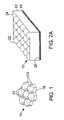
- FIG. 2Ais a perspective view of a micro-lens array with an aligned aperture mask, in accordance with one preferred embodiment of the present invention
- FIG. 2Bis a cross-sectional view of the micro-lens array with aligned aperture mask embodiment of FIG. 2A , in accordance with the present invention
- FIG. 2Cis a plan view of the aperture mask used in the embodiment of FIGS. 2A and 2B , in accordance with the present invention.
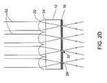
- FIG. 2Dis a cross-sectional view of the micro-lens array with aligned aperture mask embodiment of FIGS. 2A–2C , showing how light propagates through the micro-lens array/aperture mask combination, in accordance with the present invention
- FIG. 2Eis a perspective view of a micro-lens array with an aligned aperture mask, in accordance with the present invention.
- FIG. 2Fis a plan view of the aperture mask used in the embodiment of FIG. 2E , in accordance with the present invention.
- FIG. 3Ais a perspective view of a micro-lens array with an aligned aperture mask, in accordance with a second preferred embodiment of the present invention.
- FIG. 3Bis a cross-sectional view of the micro-lens array with aligned aperture mask embodiment of FIG. 3A , in accordance with the present invention
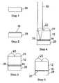
- FIGS. 4A–4Dare cross-sectional views of steps in one preferred method of fabricating a micro-lens array/aperture mask, in accordance with the present invention.
- FIGS. 5A–5Eare cross-sectional views of steps in another preferred method of fabricating a micro-lens array/aperture mask, in accordance with the present invention.
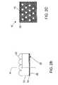
- FIG. 6is a plan view of a mask portion corresponding to a single lenslet section of a micro-lens array before an aperture is formed, in accordance with the present invention.
- FIG. 7is a plan view of a mask portion corresponding to a single lenslet section of a micro-lens array after an aperture is formed, in accordance with the present invention.
- a micro-lens array 10 made up of an assembly of lenslets 22is shown.
- the lenslets 22may be formed by “stamping” or embossing lens material 15 .
- stampingbroadly covers the process of forming shapes on a photopolymer, and curing the photopolymer material, and “stamper” broadly covers any tool used to form such shapes.
- each of the lenslets 22has a spherical sector or a like-rounded projecting portion, and a periphery 23 .
- the projecting portion of the lensletsmay be of any shape, including ellipsoidal, toroidal or aspherical.
- Each lenslet 22may be hexagonal in shape at its periphery 23 , or other shapes besides hexagonal could be used for the periphery 23 of each lenslet.
- the periphery 23defines the lenslets 22 as being only partially spherical or partially rounded surfaces. For example, lenslets 22 may form hemispheres. Lenslets 22 may be spaced at periodic or random intervals across the surface of the substrate 12 .
- the micro-lens array 10includes lenslets 22 that are formed on or attached to a substrate 12 , which has first and second surfaces, 24 and 26 , respectively.
- the lenslets 22 and the substrate 12are shown as separate elements, it should be appreciated that the substrate 12 could be the lens material 15 from which the lens array 10 is formed, as shown in the lens array 10 of FIG. 1 .
- Possible spacing patterns of the lenslets 22include having at least some of the lenslets 22 abutting one another, separating at least some of the lenslets 22 by a prescribed distance, and/or having at least some of the lenslets 22 overlap each other.
- the lenslets 22can each have similar focal lengths, or their focal lengths can vary from one another in a prescribed manner.
- each of the lenslets 22may include virtually any lens geometry known in the art which may be attached to or formed on the surface of the planar substrate 12 .
- the first and second surfaces, 24 and 26 , of the substrate 12are typically parallel to one another.
- the overall form of the planar substrate 12may be disk-like or sheet-like, although virtually any geometric form can be used.
- the planar substrate 12is typically made of glass or plastic, although any transparent material suitable for micro-lens structures known in the art may be employed.
- each lenslet 22will typically have an optical axis A, and the optical axis will typically be orthogonal to a planar surface of the substrate 12 .
- the typical micro-lens array 10is generally configured so that the optical axes A of all the lenslets 22 are parallel to one another, this need not be the case. Other configurations are possible, depending on the application.
- the aperture mask 16is preferably formed from a material that is compatible with a non-ablative aperture formation process, as will be explained in more detail below.
- Preferred mask 16 materialsinclude carbides, such as TiC, metals (e.g., Al, Cr, Cu, Zn, Se, Fe) alone or in combination with their oxides, high temperature metals (e.g., Ti, Ta, Zr, V), nitrides, oxides, selenides, tellurides, and carbon. Cermets and mixtures of these materials may also be used.
- Preferred mask 16 materialsmay also include polymers, organic black materials, and other substances substantially opaque to the electromagnetic radiation to be transmitted by the micro-lens array 10 .
- Typical thicknesses of the mask 16are on the order of 0.5 to 100 absorption lengths, depending on the desired optical properties, although other thicknesses may be used.
- the aperture mask 16includes a plurality of apertures 32 .
- the aperture mask 16preferably has one aperture 32 for each lenslet 22 in the micro-lens array 10 , with each aperture 32 precisely aligned with its respective lenslet 22 so that light input to a lenslet 22 is focused through its corresponding aperture 32 .
- FIG. 2Cis a plan view of the aperture mask 16 , showing the spaced apertures 32 in the aperture mask 16 .
- a micro-lens array 10 with an aligned aperture mask 16is shown with light 52 projected therethrough.
- the lenslet 22when light 52 is directed through a lenslet 22 , the lenslet 22 focuses and directs the light 52 so that at least a portion of it propagates through the aperture 32 .
- the light 52may be further affected by the corresponding aperture 32 . Consequently, after passing through the lenslet 22 , the light 52 can be further modified by the aperture 32 .
- Such modificationsinclude blocking a portion of the light 52 , as well as reducing cross-talk between light 52 input to multiple lenslets 22 .
- a lenticular micro-lens array 11is shown.
- the lenticular micro-lens array 11includes a substrate 12 with a top surface 24 and a bottom surface 25 . Attached to the top surface 24 are lenticular lenslets 23 consisting of linear lens structures.
- the bottom surface 25 of the substrate 12has an aperture mask 17 .
- the aperture mask 17has apertures 33 which are aligned with each corresponding lenslet 23 .
- FIG. 2Fa plan view of the mask side of the lenticular lens array is shown.
- the lenticular lens arrayincludes the mask 17 with the apertures 33 .
- the apertures 33 of the lenticular lens arrayincludes substantially linear openings in the mask 17 .
- the apertures 33run along the substrate 12 substantially in alignment with each corresponding lenslet 23 .
- FIGS. 3A and 3Billustrate a second preferred embodiment of the invention is shown.
- the embodiment of FIGS. 3A and 3Bis similar to the embodiment of FIGS. 2A–2D , with the addition of a substrate 28 that is attached to the aperture mask 16 .
- the substrate 28may also be reflective, partially reflective or diffusive to the electromagnetic radiation that will be input to the micro-lens array 10 .
- the substrate 28may provide mechanical support to the micro-lens array 10 , protect the aperture mask 16 and/or filter, polarize or otherwise modify light projected by the lenslets 22 through the apertures 32 .
- FIGS. 4A–4Dare cross-sectional views of steps in one preferred method of fabricating the micro-lens array/aperture mask of the present invention. For illustrative purposes, cross-sectional views showing the formation of two lenslets and corresponding apertures are shown.
- An initial step of the methodis forming the micro-lens array ( FIG. 4A ), which includes providing a substrate 12 made of, for example, a polycarbonate or acrylic plastic thick enough to provide a desired level of mechanical stability.
- a material from which the micro-lens array is to be replicated on a surface 24 of the transparent substrate 12is then applied to the substrate 12 (not shown). This material may be, for example, a photopolymer epoxy, a polycarbonate, or PMMA resin.
- This materialis then patterned to form the individual lenses 22 in the micro-lens array.
- This patterning stepmay be performed by any one of a variety of methods.
- the patterning stepmay be performed in accordance with a stamping operation performed by a master, which contains the lens pattern thereon.
- the patterning stepmay also be performed by embossing or other techniques.
- a second stepincludes coating a second surface 16 of the substrate 12 with a thin layer 16 of masking material.
- the thickness of this layermay vary with the material employed, but a thickness of from 0.5 to 100 absorption lengths has been found to be preferable.
- Coating techniquesinclude e-beam vacuum deposition, sputtering, chemical vapor deposition, as well as other film-deposition techniques.
- preferred masking materialsinclude carbides, such as TiC, metals (e.g., Al, Cr, Cu, Zn, Se, Fe) alone or in combination with their oxides, high temperature metals (e.g., Ti, Ta, Zr, V), nitrides, oxides, selenides, tellurides, and carbon.
- Cermets and mixtures of these materialsmay also be used.
- Preferred masking materialsmay also include polymers, organic black materials, and other substances substantially opaque to the electromagnetic radiation to be transmitted by the micro-lens array 10 .
- any substance substantially opaque to the electromagnetic radiation to be transmitted by the micro-lens array and that is compatible with a non-ablative aperture formation processmay be used.
- a third stepincludes forming apertures 32 in mask layer 16 which are aligned with respective lenslets 22 . This is preferably performed by directing pulsed laser radiation or similarly intense electromagnetic radiation 62 through the curved surface of each lenslet 22 , which focuses the radiation 62 to an area 42 on the mask layer 16 .
- the electromagnetic radiation 62is preferably pulsed with energy sufficient to form an aperture by means of a non-ablative process, but preferably not so much energy so as to vaporize the material or degrade the desired optical properties of the lenslets 22 and/or the associated substrates.
- a typical range for pulseswould include irradiance levels above 0.1 mJ/cm 2 and pulse widths shorter than 1 ms, however, the precise combination of irradiance and pulse widths required will depend on many parameters, including the type of material used for the mask layer 16 the thickness of the mask layer and the precise positioning of the aperture. For example, for a mask layer 16 made of TiC material with a thickness in the range of 0.5 to 100 absorption lengths, a combination of pulses with irradiances of 1 mJ/cm 2 to 5 mJ/cm 2 and pulse widths on the order of 10 ns have proven effective.
- the optimum wavelengths of the electromagnetic radiation 62 usedwill depend on the spectral absorption properties of the material used for the mask layer 16 .
- a mask layer 16 made of TiCa wide range of wavelengths, from infrared through ultraviolet have proven effective.
- the apertures 32may be formed one at a time by serially illuminating each lenslet 22 in the micro-lens array with the pulsed laser radiation, or other electromagnetic radiation. Alternatively, they may also be formed by simultaneously illuminating two or more of the lenslets 22 , using either separate electromagnetic beams (e.g., separate pulsed laser beams) or a single electromagnetic beam (e.g., a single pulsed laser beam) that has been spatially expanded to cover two or more of the lenslets 22 .
- separate electromagnetic beamse.g., separate pulsed laser beams
- a single electromagnetic beame.g., a single pulsed laser beam
- the thickness of the substrate 12can determine whether the mask layer 16 lies at the focal point of the lenslet 22 .
- the size of the irradiated area 42and therefore the size of the aperture, may be changed.
- the smallest aperture 32 that can be formed by the lensletis achieved by adjusting the thickness of the substrate 12 so that the mask layer 16 lies at the focal plane of the lenslet 22 .
- the aperture sizeis dictated by the diffraction limited spot size of the radiation at the focal plane and any aberrations that may be present.
- non-ablative processis used to describe a process in which apertures are patterned in a mask layer by depositing sufficient electromagnetic energy at desired points on the mask layer so that at least one of the following mechanisms takes place: (1) a “contraction” mechanism in which the mask layer material heats up and contracts to form an aperture without vaporizing or ablating the mask layer material; (2) a “phase change” mechanism in which the mask layer material undergoes a phase change into a form which is substantially transparent to radiation at desired predetermined wavelengths; (3) a “mechanical deformation” mechanism in which the mask layer material undergoes mechanical deformation; and/or (4) a “chemical” mechanism in which the mask layer material undergoes a chemical transformation, such as oxidation.
- the mask layer materialis preferably heated to a point in which the surface tension of the mask layer material overcomes the strength of the mask layer material. This results in the mask layer material “pulling back” or contracting to form a clear aperture, with rolled back material at the perimeter of the aperture. Depending on the mask layer material, it may not be necessary to heat the mask layer area where the aperture is to be formed to the melting point of the mask layer material.
- the non-ablative process used in the present inventionexhibits many benefits over traditional ablative processes. If an ablative process were to be used to create the apertures, the mask layer material would have to be heated to the material's boiling temperature. In order to achieve these high temperatures, a very high power laser with very short laser pulses would have to be used. Lasers that produce pulse widths of less than 1 ns, and typically pico-second pulses, are needed for ablative processes. These types of lasers are expensive, difficult to work with, and have limited wavelength ranges.
- mask layer materials with relatively low boiling temperatureswould need to be used in order to avoid heating the surrounding areas (e.g., the substrate and lenslets) to the point where these areas would be damaged. This would effectively limit the choice of materials for the mask layer.
- the non-ablative process used in the present inventiondoes not require that the mask layer material be heated to the material's boiling point. Accordingly, a much wider selection of materials can be used in the present invention, including many high temperature materials, as listed above. In addition, a wider selection of radiation sources may be used with the non-ablative process used in the present invention.
- An optional fifth stepincludes attaching a substrate 28 of polycarbonate or other material to the mask layer 16 preferably with an optical adhesive.
- the substrate 28may be optically active and/or may merely serve to protect the mask layer 16 and provide additional mechanical support to the micro-lens array.
- FIGS. 5A–5Eare cross-sectional views of steps in a second preferred method of fabricating the micro-lens array/aperture mask of the present invention.
- An initial step of the method( FIG. 5A ), a substrate is provided that is made of, for example, polycarbonate or acrylic plastic thick enough to provide a desired level of mechanical stability.
- the substrate 28is preferably optically transparent to the electromagnetic radiation that will be input to the completed micro-lens array.
- a second stepincludes applying a mask layer 16 to the substrate 28 using techniques similar to those discussed above in connection with the method of FIGS. 4A–4D .
- a third stepinvolves forming the micro-lens array, which includes providing a substrate 12 made of, for example, a polycarbonate or acrylic plastic thick enough to provide a desired level of mechanical stability.
- the substrate 12is preferably attached to the mask layer 16 with an optical adhesive.
- a material from which the micro-lens array is to be replicated on a surface 24 of the transparent substrate 12is then applied to the substrate 12 (not shown).
- This materialmay be, for example, a photopolymer epoxy, a polycarbonate, or PMMA resin.
- This materialis then patterned to form the individual lenses 22 in the micro-lens array.
- This patterning stepmay be performed by any one of a variety of methods. Preferably, the patterning step is performed in accordance with a stamping operation performed by a master, which contains the lens pattern thereon.
- a fourth stepincludes forming apertures 32 in mask layer 16 which are aligned with respective lenslets 22 . As discussed above, this is preferably performed by directing pulsed laser radiation or similarly intense electromagnetic radiation 62 through the curved surface of each lenslet 22 , which focuses the radiation 62 to an area 42 on the mask layer 16 .
- the electromagnetic radiation 62is preferably pulsed with energy sufficient to form an aperture by means of a non-ablative process, but preferably not so much energy as to vaporize the material or degrade the desired optical properties of the lenslets 22 and/or the associated substrates.
- a typical range for pulseswould include irradiance levels above 0.1 mJ/cm 2 and pulse widths shorter than 1 ms, however, the precise combination of irradiance and pulse widths required will depend on many parameters, including the type of material used for the mask layer 16 the thickness of the mask layer and the precise positioning of the aperture. For example, for a mask layer 16 made of TiC material with a thickness in the range of 0.5 to 100 absorption lengths, a combination of pulses with irradiances of 1 mJ/cm 2 to 5 mJ/cm 2 and pulse widths on the order of 10 ns have proven effective.
- the optimum wavelengths of the electromagnetic radiation 62 usedwill depend on the spectral absorption properties of the material used for the mask layer 16 .
- a mask layer 16 made of TiCa wide range of wavelengths, from infrared through ultraviolet have proven effective.
- the apertures 32may be formed one at a time by serially illuminating each lenslet 22 in the micro-lens array with the pulsed laser radiation, or other electromagnetic radiation. Alternatively, they may also be formed by simultaneously illuminating two or more of the lenslets 22 , using either separate electromagnetic beams (e.g., separate pulsed laser beams) or a single electromagnetic beam (e.g., a single pulsed laser beam) that has been spatially expanded to cover two or more of the lenslets 22 .
- separate electromagnetic beamse.g., separate pulsed laser beams
- a single electromagnetic beame.g., a single pulsed laser beam
- the thickness of the substrate 12can determine whether the mask layer 16 lies at the focal plane of the lenslet 22 .
- the size of the irradiated area 42and therefore the size of the aperture, may be changed.
- the smallest aperture 32 that can be formed by the lensletis achieved by adjusting the thickness of the substrate 12 so that the mask layer 16 lies at the focal plane of the lenslet 22 .
- the aperture sizeis dictated by the diffraction limited spot size of the radiation at the focal plane.
- non-ablative processis used herein to describe a process in which apertures are formed or patterned in the mask layer, preferably without vaporizing or ablating the mask layer material. Use of such a process is of particular importance in the fabrication method of FIGS. 5A–5E , since the mask layer 16 is positioned between other layers of material (e.g., the two substrates 12 and 28 ). An ablative process is particularly inappropriate for this embodiment.
- FIGS. 5 and 6are plan views of a mask portion corresponding to a single lenslet section of a micro-lens array before and after an aperture is formed, respectively.
- the electromagnetic radiationhas been focused onto an area 42 on the mask layer 16 .
- the energy delivered to the area 42is controlled so as to initiate a non-ablative aperture formation process.
- an amount of electromagnetic energyis deposited at desired areas on the mask layer 16 sufficient to melt the mask layer material and cause it to contract to form an aperture 32 , as shown in FIG. 7 .
- the shape of the aperture 32will depend on the spatial profile of that portion of the electromagnetic radiation that deposits the required amount of energy on the mask layer 16 .
- the aperture 32 shown in FIG. 7is generally circular in shape, any other aperture shape can be produced while still falling within the scope of the present invention, including, but not limited to, square, rectangular, polygonal and elliptical shapes.
Landscapes
- Physics & Mathematics (AREA)
- General Physics & Mathematics (AREA)
- Optics & Photonics (AREA)
- Engineering & Computer Science (AREA)
- Manufacturing & Machinery (AREA)
- Health & Medical Sciences (AREA)
- Ophthalmology & Optometry (AREA)
- Mechanical Engineering (AREA)
- Laser Beam Processing (AREA)
- Optical Elements Other Than Lenses (AREA)
Abstract
Description
Claims (75)
Priority Applications (7)
| Application Number | Priority Date | Filing Date | Title |
|---|---|---|---|
| US10/452,238US6967779B2 (en) | 1998-04-15 | 2003-06-03 | Micro-lens array with precisely aligned aperture mask and methods of producing same |
| AU2004248570AAU2004248570C1 (en) | 2003-06-03 | 2004-06-02 | Micro-lens array with precisely aligned aperture mask and methods of producing same |
| JP2006515117AJP2007526491A (en) | 2003-06-03 | 2004-06-02 | Microlens array with precisely aligned aperture mask and method of manufacturing the same |
| CA002527602ACA2527602A1 (en) | 2003-06-03 | 2004-06-02 | Micro-lens array with precisely aligned aperture mask and methods of producing same |
| KR1020057023035AKR20060038382A (en) | 2003-06-03 | 2004-06-02 | Microlens array with precisely aligned aperture mask and manufacturing method thereof |
| PCT/US2004/017449WO2004111706A2 (en) | 2003-06-03 | 2004-06-02 | Micro-lens array with precisely aligned aperture mask and methods of producing same |
| EP04754126AEP1629316A4 (en) | 2003-06-03 | 2004-06-02 | Micro-lens array with precisely aligned aperture mask and methods of producing same |
Applications Claiming Priority (4)
| Application Number | Priority Date | Filing Date | Title |
|---|---|---|---|
| US6090698A | 1998-04-15 | 1998-04-15 | |
| US09/521,236US6483612B2 (en) | 1998-04-15 | 2000-04-05 | Projection screen apparatus including holographic optical element |
| US10/120,785US6788460B2 (en) | 1998-04-15 | 2002-04-12 | Projection screen apparatus |
| US10/452,238US6967779B2 (en) | 1998-04-15 | 2003-06-03 | Micro-lens array with precisely aligned aperture mask and methods of producing same |
Related Parent Applications (1)
| Application Number | Title | Priority Date | Filing Date |
|---|---|---|---|
| US10/120,785Continuation-In-PartUS6788460B2 (en) | 1993-05-12 | 2002-04-12 | Projection screen apparatus |
Publications (2)
| Publication Number | Publication Date |
|---|---|
| US20040017612A1 US20040017612A1 (en) | 2004-01-29 |
| US6967779B2true US6967779B2 (en) | 2005-11-22 |
Family
ID=33551266
Family Applications (1)
| Application Number | Title | Priority Date | Filing Date |
|---|---|---|---|
| US10/452,238Expired - Fee RelatedUS6967779B2 (en) | 1998-04-15 | 2003-06-03 | Micro-lens array with precisely aligned aperture mask and methods of producing same |
Country Status (7)
| Country | Link |
|---|---|
| US (1) | US6967779B2 (en) |
| EP (1) | EP1629316A4 (en) |
| JP (1) | JP2007526491A (en) |
| KR (1) | KR20060038382A (en) |
| AU (1) | AU2004248570C1 (en) |
| CA (1) | CA2527602A1 (en) |
| WO (1) | WO2004111706A2 (en) |
Cited By (74)
| Publication number | Priority date | Publication date | Assignee | Title |
|---|---|---|---|---|
| US20050254132A1 (en)* | 2004-05-14 | 2005-11-17 | Ali M Z | Methods for producing a black matrix on a lenticular lens |
| US20060164729A1 (en)* | 2004-02-12 | 2006-07-27 | Bright View Technologies, Inc. | Front-projection screens including reflecting layers and optically absorbing layers having apertures therein, and methods of fabricating the same |
| US20060256442A1 (en)* | 2005-05-10 | 2006-11-16 | Seiko Epson Corporation | Microlens, optical plate, diffusing plate, light guide plate, backlight, projection screen, projection system, electro-optical device, electronic apparatus, and method for manufacturing a microlens |
| US20070035154A1 (en)* | 2005-01-31 | 2007-02-15 | Edscha Cabrio-Dachsysteme Gmbh | Top for a convertible vehicle |
| US20070127129A1 (en)* | 2005-12-07 | 2007-06-07 | Bright View Technologies, Inc. | Optically transparent electromagnetic interference (EMI) shields for direct-view displays |
| US20070127098A1 (en)* | 2005-12-07 | 2007-06-07 | Bright View Technologies, Inc. | Contrast enhancement films for direct-view displays and fabrication methods therefor |
| US20070195406A1 (en)* | 2006-02-22 | 2007-08-23 | Wood Robert L | Screens, microstructure templates, and methods of forming the same |
| US20070237490A1 (en)* | 2006-03-22 | 2007-10-11 | Francis Mark Reininger | Fiber coupled artificial compound eye |
| US20070253058A1 (en)* | 2006-05-01 | 2007-11-01 | Bright View Technologies, Inc. | Brightness enhancement structures including optical microstructures to provide elliptical diffusion patterns and methods of fabricating and operating the same |
| US20070258149A1 (en)* | 2006-05-08 | 2007-11-08 | Bright View Technologies, Inc. | Methods and Apparatus for Processing a Pulsed Laser Beam to Create Apertures Through Microlens Arrays, and Products Produced Thereby |
| US20070292770A1 (en)* | 2006-06-15 | 2007-12-20 | The Boeing Company | Photolithographic method and apparatus employing a polychromatic mask |
| US20080084611A1 (en)* | 2006-10-05 | 2008-04-10 | Bright View Technologies, Inc. | Methods and Apparatus for Creating Apertures Through Microlens Arrays Using Curved Cradles, and Products Produced Thereby |
| US20080211991A1 (en)* | 2007-02-09 | 2008-09-04 | Bright View Technologies, Inc. | High contrast liquid crystal displays |
| US20080218853A1 (en)* | 2007-03-06 | 2008-09-11 | Ostendo Technologies, Inc. | Micro-structure based screen system for use in rear projection array display systems |
| US7561323B2 (en) | 2004-09-27 | 2009-07-14 | Idc, Llc | Optical films for directing light towards active areas of displays |
| US7587109B1 (en) | 2008-09-02 | 2009-09-08 | Spectral Imaging Laboratory | Hybrid fiber coupled artificial compound eye |
| US7603001B2 (en) | 2006-02-17 | 2009-10-13 | Qualcomm Mems Technologies, Inc. | Method and apparatus for providing back-lighting in an interferometric modulator display device |
| US7630123B2 (en) | 2004-09-27 | 2009-12-08 | Qualcomm Mems Technologies, Inc. | Method and device for compensating for color shift as a function of angle of view |
| US7710636B2 (en) | 2004-09-27 | 2010-05-04 | Qualcomm Mems Technologies, Inc. | Systems and methods using interferometric optical modulators and diffusers |
| US7710632B2 (en) | 2004-09-27 | 2010-05-04 | Qualcomm Mems Technologies, Inc. | Display device having an array of spatial light modulators with integrated color filters |
| US7719747B2 (en) | 2004-09-27 | 2010-05-18 | Qualcomm Mems Technologies, Inc. | Method and post structures for interferometric modulation |
| US7777954B2 (en) | 2007-01-30 | 2010-08-17 | Qualcomm Mems Technologies, Inc. | Systems and methods of providing a light guiding layer |
| US7808706B2 (en) | 2004-02-12 | 2010-10-05 | Tredegar Newco, Inc. | Light management films for displays |
| US7806547B2 (en) | 2006-07-14 | 2010-10-05 | Light Prescriptions Innovators, Llc | Brightness-enhancing film |
| US7807488B2 (en) | 2004-09-27 | 2010-10-05 | Qualcomm Mems Technologies, Inc. | Display element having filter material diffused in a substrate of the display element |
| US7813026B2 (en) | 2004-09-27 | 2010-10-12 | Qualcomm Mems Technologies, Inc. | System and method of reducing color shift in a display |
| US7845841B2 (en) | 2006-08-28 | 2010-12-07 | Qualcomm Mems Technologies, Inc. | Angle sweeping holographic illuminator |
| US7855824B2 (en) | 2004-03-06 | 2010-12-21 | Qualcomm Mems Technologies, Inc. | Method and system for color optimization in a display |
| US7864395B2 (en) | 2006-10-27 | 2011-01-04 | Qualcomm Mems Technologies, Inc. | Light guide including optical scattering elements and a method of manufacture |
| US7898521B2 (en) | 2004-09-27 | 2011-03-01 | Qualcomm Mems Technologies, Inc. | Device and method for wavelength filtering |
| US7907319B2 (en) | 1995-11-06 | 2011-03-15 | Qualcomm Mems Technologies, Inc. | Method and device for modulating light with optical compensation |
| US7911428B2 (en) | 2004-09-27 | 2011-03-22 | Qualcomm Mems Technologies, Inc. | Method and device for manipulating color in a display |
| US20110069249A1 (en)* | 2009-09-21 | 2011-03-24 | Coretronic Corporation | Backlight module and liquid crystal display apparatus |
| US20110085241A1 (en)* | 2009-10-13 | 2011-04-14 | Purchase Ken G | Transmissive optical microstructure substrates that produce visible patterns |
| US7928928B2 (en) | 2004-09-27 | 2011-04-19 | Qualcomm Mems Technologies, Inc. | Apparatus and method for reducing perceived color shift |
| US8004743B2 (en) | 2006-04-21 | 2011-08-23 | Qualcomm Mems Technologies, Inc. | Method and apparatus for providing brightness control in an interferometric modulator (IMOD) display |
| US8040588B2 (en) | 2004-09-27 | 2011-10-18 | Qualcomm Mems Technologies, Inc. | System and method of illuminating interferometric modulators using backlighting |
| US8040589B2 (en) | 2008-02-12 | 2011-10-18 | Qualcomm Mems Technologies, Inc. | Devices and methods for enhancing brightness of displays using angle conversion layers |
| US8045252B2 (en) | 2004-02-03 | 2011-10-25 | Qualcomm Mems Technologies, Inc. | Spatial light modulator with integrated optical compensation structure |
| US8049951B2 (en) | 2008-04-15 | 2011-11-01 | Qualcomm Mems Technologies, Inc. | Light with bi-directional propagation |
| US8061882B2 (en) | 2006-10-06 | 2011-11-22 | Qualcomm Mems Technologies, Inc. | Illumination device with built-in light coupler |
| US8068710B2 (en) | 2007-12-07 | 2011-11-29 | Qualcomm Mems Technologies, Inc. | Decoupled holographic film and diffuser |
| US8111446B2 (en) | 2004-09-27 | 2012-02-07 | Qualcomm Mems Technologies, Inc. | Optical films for controlling angular characteristics of displays |
| US20120091703A1 (en)* | 2009-04-06 | 2012-04-19 | Reserve Bank Of Australia | Security document with an optically variable image and method of manufacture |
| US8193441B2 (en) | 2007-12-17 | 2012-06-05 | Qualcomm Mems Technologies, Inc. | Photovoltaics with interferometric ribbon masks |
| US8231257B2 (en) | 2009-01-13 | 2012-07-31 | Qualcomm Mems Technologies, Inc. | Large area light panel and screen |
| US8300304B2 (en) | 2008-02-12 | 2012-10-30 | Qualcomm Mems Technologies, Inc. | Integrated front light diffuser for reflective displays |
| US8348489B2 (en) | 2008-01-30 | 2013-01-08 | Qualcomm Mems Technologies, Inc. | Thin illumination system |
| US8362987B2 (en) | 2004-09-27 | 2013-01-29 | Qualcomm Mems Technologies, Inc. | Method and device for manipulating color in a display |
| US8368981B2 (en) | 2006-10-10 | 2013-02-05 | Qualcomm Mems Technologies, Inc. | Display device with diffractive optics |
| US8393777B2 (en) | 2005-07-28 | 2013-03-12 | Light Prescriptions Innovators, Llc | Etendue-conserving illumination-optics for backlights and frontlights |
| US8402647B2 (en) | 2010-08-25 | 2013-03-26 | Qualcomm Mems Technologies Inc. | Methods of manufacturing illumination systems |
| US20130100647A1 (en)* | 2010-06-30 | 2013-04-25 | 3M Innovative Properties Company | Light directing film |
| US8576489B2 (en) | 2010-08-02 | 2013-11-05 | Spectral Imaging Laboratory | Multihybrid artificial compound eye with varied ommatidia |
| US8670171B2 (en) | 2010-10-18 | 2014-03-11 | Qualcomm Mems Technologies, Inc. | Display having an embedded microlens array |
| US8674616B2 (en) | 2008-10-10 | 2014-03-18 | Qualcomm Mems Technologies, Inc. | Distributed illumination system |
| US8721149B2 (en) | 2008-01-30 | 2014-05-13 | Qualcomm Mems Technologies, Inc. | Illumination device having a tapered light guide |
| US8848294B2 (en) | 2010-05-20 | 2014-09-30 | Qualcomm Mems Technologies, Inc. | Method and structure capable of changing color saturation |
| US8872085B2 (en) | 2006-10-06 | 2014-10-28 | Qualcomm Mems Technologies, Inc. | Display device having front illuminator with turning features |
| US8902484B2 (en) | 2010-12-15 | 2014-12-02 | Qualcomm Mems Technologies, Inc. | Holographic brightness enhancement film |
| US8928967B2 (en) | 1998-04-08 | 2015-01-06 | Qualcomm Mems Technologies, Inc. | Method and device for modulating light |
| US8971675B2 (en) | 2006-01-13 | 2015-03-03 | Qualcomm Mems Technologies, Inc. | Interconnect structure for MEMS device |
| US8979349B2 (en) | 2009-05-29 | 2015-03-17 | Qualcomm Mems Technologies, Inc. | Illumination devices and methods of fabrication thereof |
| US9019183B2 (en) | 2006-10-06 | 2015-04-28 | Qualcomm Mems Technologies, Inc. | Optical loss structure integrated in an illumination apparatus |
| US9025235B2 (en) | 2002-12-25 | 2015-05-05 | Qualcomm Mems Technologies, Inc. | Optical interference type of color display having optical diffusion layer between substrate and electrode |
| US9110289B2 (en) | 1998-04-08 | 2015-08-18 | Qualcomm Mems Technologies, Inc. | Device for modulating light with multiple electrodes |
| DE102015010077A1 (en) | 2015-08-07 | 2017-02-09 | Karlsruher Institut für Technologie | Method for producing optoelectronically active components |
| WO2018070977A1 (en)* | 2016-10-10 | 2018-04-19 | Halliburton Energy Services, Inc. | Optical interface with surface coating |
| US20190063909A1 (en)* | 2016-03-23 | 2019-02-28 | Enplas Corporation | Marker |
| US10270947B2 (en) | 2016-09-15 | 2019-04-23 | Microsoft Technology Licensing, Llc | Flat digital image sensor |
| USD874715S1 (en) | 2018-03-07 | 2020-02-04 | Myotek Holdings, Inc. | LED spot lamp lens |
| US10838255B2 (en) | 2014-10-07 | 2020-11-17 | Corning Incorporated | Direct view display device and light unit for direct view display device |
| US11148230B2 (en)* | 2017-11-01 | 2021-10-19 | Samsung Display Co., Ltd. | Method of manufacturing deposition mask |
| US11911852B2 (en)* | 2016-02-08 | 2024-02-27 | Primes GmbH Meßtechnik für die Produktion mit Laserstrahlung | Analysis of laser beams in systems for a generative manufacturing process |
Families Citing this family (20)
| Publication number | Priority date | Publication date | Assignee | Title |
|---|---|---|---|---|
| US7116404B2 (en)* | 2004-06-30 | 2006-10-03 | Asml Netherlands B.V | Lithographic apparatus and device manufacturing method |
| KR100623014B1 (en)* | 2004-08-28 | 2006-09-19 | 엘지전자 주식회사 | Micromatrix array sheet with black matrix and manufacturing method |
| US7433122B2 (en)* | 2004-11-12 | 2008-10-07 | Infocus Corporation | Front-projection screen with subsurface diffusion targets |
| US20060131683A1 (en)* | 2004-12-17 | 2006-06-22 | Eastman Kodak Company | Microlens array |
| KR100624462B1 (en)* | 2005-03-04 | 2006-09-19 | 삼성전자주식회사 | Method of manufacturing patterned record carrier |
| US7092166B1 (en) | 2005-04-25 | 2006-08-15 | Bright View Technologies, Inc. | Microlens sheets having multiple interspersed anamorphic microlens arrays |
| KR100796597B1 (en)* | 2006-07-14 | 2008-01-21 | 삼성에스디아이 주식회사 | Laser irradiation apparatus and manufacturing method of organic light emitting device using same |
| US7800825B2 (en)* | 2006-12-04 | 2010-09-21 | 3M Innovative Properties Company | User interface including composite images that float |
| DE102007056402A1 (en)* | 2007-11-23 | 2009-05-28 | Osram Gesellschaft mit beschränkter Haftung | Optical component and lighting device |
| JP5629965B2 (en)* | 2008-07-01 | 2014-11-26 | 凸版印刷株式会社 | Image forming body manufacturing method and laminate |
| DE102012220570B4 (en)* | 2012-11-12 | 2022-07-14 | Osram Gmbh | PROJECTION ARRANGEMENT |
| KR102100285B1 (en)* | 2013-09-26 | 2020-04-13 | 엘지디스플레이 주식회사 | Method Of Manufacturing Maskless Exposure Apparatus |
| WO2016077309A2 (en)* | 2014-11-12 | 2016-05-19 | Corning Incorporated | Contrast enhancement sheet and display device comprising the same |
| CN107479315A (en)* | 2016-06-08 | 2017-12-15 | 深圳市光峰光电技术有限公司 | A kind of movie theatre viewing system |
| DE102016010383B4 (en) | 2016-08-30 | 2019-02-21 | Preh Gmbh | Method for producing a lenticular sheet layer construction |
| DE102016119880A1 (en)* | 2016-10-19 | 2018-04-19 | HELLA GmbH & Co. KGaA | Lighting device for vehicles |
| FR3084207B1 (en)* | 2018-07-19 | 2021-02-19 | Isorg | OPTICAL SYSTEM AND ITS MANUFACTURING PROCESS |
| WO2021255596A1 (en)* | 2020-06-17 | 2021-12-23 | 3M Innovative Properties Company | Optical construction including lens film and mask layer |
| CN114545532A (en)* | 2020-11-18 | 2022-05-27 | 深圳市光鉴科技有限公司 | Mask-embedded microlens array and method of use |
| US12399059B2 (en) | 2020-12-18 | 2025-08-26 | 3M Innovative Properties Company | Optical construction including lens film and mask |
Citations (84)
| Publication number | Priority date | Publication date | Assignee | Title |
|---|---|---|---|---|
| US1942841A (en) | 1931-01-19 | 1934-01-09 | Shimizu Takeo | Daylight screen |
| US3893748A (en) | 1973-11-30 | 1975-07-08 | Eastman Kodak Co | Low scintillation, multi-component projection screen |
| US4076384A (en) | 1975-05-02 | 1978-02-28 | Agfa-Gevaert, A.G. | Rear-projection viewing screen |
| US4083626A (en) | 1975-04-04 | 1978-04-11 | Fuji Photo Film Co., Ltd. | Rear projection screens |
| US4172219A (en) | 1975-03-15 | 1979-10-23 | Agfa-Gevaert, A.G. | Daylight projection screen and method and apparatus for making the same |
| US4268118A (en) | 1979-09-05 | 1981-05-19 | Minnesota Mining And Manufacturing Company | Sheeting useful as a projection screen |
| US4418986A (en) | 1981-04-07 | 1983-12-06 | Mitsubishi Rayon Co., Ltd. | Rear projection screen |
| US4490010A (en) | 1982-06-10 | 1984-12-25 | Dai Nippon Insatsu Kabushiki Kaisha | Rear projection screen |
| US4523849A (en) | 1982-02-11 | 1985-06-18 | The United States Of America As Represented By The United States Department Of Energy | Front lighted optical tooling method and apparatus |
| US4666248A (en) | 1985-12-20 | 1987-05-19 | U. S. Philips Corporation | Rear-projection screen |
| US4773731A (en) | 1987-08-28 | 1988-09-27 | North American Philips Corp. | One-piece projection screen |
| US4799137A (en) | 1987-03-24 | 1989-01-17 | Minnesota Mining And Manufacturing Company | Reflective film |
| US4874228A (en) | 1987-03-24 | 1989-10-17 | Minnesota Mining And Manufacturing Company | Back-lit display |
| US4961642A (en) | 1988-07-18 | 1990-10-09 | Hitachi, Ltd. | Projection type display device for monitoring at short distance |
| US4969732A (en) | 1988-02-25 | 1990-11-13 | Thorn Emi Plc | Display device |
| US4982214A (en) | 1988-05-07 | 1991-01-01 | Canon Kabushiki Kaisha | Focusing screen |
| US5054885A (en) | 1988-10-11 | 1991-10-08 | Minnesota Mining And Manfuacturing Company | Light fixture including a partially collimated beam of light and reflective prisms having peaks lying on a curved surface |
| JPH03243932A (en) | 1990-02-22 | 1991-10-30 | Canon Inc | Rear projection receiver |
| EP0488590A1 (en) | 1990-11-30 | 1992-06-03 | THORN EMI plc | Display device |
| US5122905A (en) | 1989-06-20 | 1992-06-16 | The Dow Chemical Company | Relective polymeric body |
| US5166824A (en) | 1990-10-30 | 1992-11-24 | Hitachi, Ltd. | Rear projection screen and manufacturing method therefor as well as molding die for shaping rear projection screen, overhead projector and projection television set |
| US5190370A (en) | 1991-08-21 | 1993-03-02 | Minnesota Mining And Manufacturing Company | High aspect ratio lighting element |
| US5193015A (en) | 1989-10-05 | 1993-03-09 | Thorn Emi Plc | Cholesteric liquid crystal screen which reflects substantially all of the projected light |
| US5223869A (en) | 1990-02-20 | 1993-06-29 | Canon Kabushiki Kaisha | Projector |
| JPH05313153A (en) | 1992-05-11 | 1993-11-26 | Canon Inc | Liquid crystal panel and its manufacture |
| US5333072A (en) | 1992-12-31 | 1994-07-26 | Minnesota Mining And Manufacturing Company | Reflective liquid crystal display overhead projection system using a reflective linear polarizer and a fresnel lens |
| US5337106A (en) | 1993-06-09 | 1994-08-09 | Kowa Company, Ltd. | Liquid-crystal image director for single-lens-reflex camera |
| US5337179A (en) | 1992-07-27 | 1994-08-09 | Hodges Marvin P | Flexible controllable optical surface and method of making the same |
| WO1994029768A1 (en) | 1993-06-15 | 1994-12-22 | Durand Limited | Randomised mask for a diffusing screen |
| US5381309A (en) | 1993-09-30 | 1995-01-10 | Honeywell Inc. | Backlit display with enhanced viewing properties |
| US5404076A (en) | 1990-10-25 | 1995-04-04 | Fusion Systems Corporation | Lamp including sulfur |
| EP0657769A1 (en) | 1993-12-10 | 1995-06-14 | Koninklijke Philips Electronics N.V. | Image projection system |
| US5442482A (en) | 1990-05-21 | 1995-08-15 | Johnson; William N. H. | Microlens screens, photopolymerisable materials and artifacts utilising the same |
| US5453859A (en) | 1993-06-03 | 1995-09-26 | Matsushita Electric Industrial Co., Ltd. | Polarization beam splitter and projection display apparatus |
| US5467154A (en) | 1992-02-20 | 1995-11-14 | Kopin Corporation | Projection monitor |
| WO1995034832A1 (en) | 1992-12-15 | 1995-12-21 | Thomson-Csf | Holographic projection screen and method for its production |
| US5486949A (en) | 1989-06-20 | 1996-01-23 | The Dow Chemical Company | Birefringent interference polarizer |
| US5496668A (en) | 1992-12-22 | 1996-03-05 | Wisconsin Alumni Research Foundation | Formation of microstructures using a preformed photoresist sheet |
| US5504391A (en) | 1992-01-29 | 1996-04-02 | Fusion Systems Corporation | Excimer lamp with high pressure fill |
| US5557343A (en) | 1994-01-28 | 1996-09-17 | Matsushita Electric Industrial, Co., Ltd. | Optical system including a reflecting polarizer for a rear projection picture display apparatus |
| US5563738A (en) | 1993-09-03 | 1996-10-08 | Jenmar Visual Systems | Light transmitting and dispersing filter having low reflectance |
| US5615045A (en) | 1992-12-25 | 1997-03-25 | Sony Corporation | Screen of projection display |
| US5626800A (en) | 1995-02-03 | 1997-05-06 | Minnesota Mining And Manufacturing Company | Prevention of groove tip deformation in brightness enhancement film |
| US5642226A (en) | 1995-01-18 | 1997-06-24 | Rosenthal; Bruce A. | Lenticular optical system |
| US5644431A (en) | 1990-05-18 | 1997-07-01 | University Of Arkansas, N.A. | Directional image transmission sheet and method of making same |
| WO1997027606A1 (en) | 1996-01-26 | 1997-07-31 | Fusion Lighting, Inc. | Microwawe lamp with multi-purpose rotary motor |
| US5657408A (en) | 1994-12-23 | 1997-08-12 | Alliedsignal Inc. | Optical device comprising a plurality of units having at least two geometrically-differentiated tapered optical waveguides therein |
| US5661531A (en) | 1996-01-29 | 1997-08-26 | Rainbow Displays Inc. | Tiled, flat-panel display having invisible seams |
| US5670842A (en) | 1990-10-25 | 1997-09-23 | Fusion Lighting Inc | Method and apparatus for igniting electroeless lamp discharge |
| JPH09258007A (en) | 1996-03-22 | 1997-10-03 | Victor Co Of Japan Ltd | Production of microlens array and production of optical recording medium having microlens array |
| US5688064A (en) | 1996-10-30 | 1997-11-18 | Fusion Lighting, Inc. | Method and apparatus for coupling bulb stem to rotatable motor shaft |
| US5694246A (en) | 1994-01-03 | 1997-12-02 | Omron Corporation | Method of manufacturing lens array |
| US5692820A (en) | 1992-02-20 | 1997-12-02 | Kopin Corporation | Projection monitor |
| JPH1039769A (en) | 1996-07-19 | 1998-02-13 | Toray Ind Inc | Micro lens array sheet |
| JPH10123623A (en) | 1996-10-16 | 1998-05-15 | Casio Comput Co Ltd | Transmission projection screen |
| US5796499A (en) | 1997-02-28 | 1998-08-18 | Polaroid Corporation | Transmission holographic diffuser made and used to effect lateral color constancy in rear screen projection display systems |
| US5801794A (en) | 1994-07-08 | 1998-09-01 | Thomson-Csf | Color display device in which the area of a spherical lens equals the area of a set of RGB sub-pixels |
| JPH10239503A (en) | 1997-02-26 | 1998-09-11 | Sharp Corp | Micro lens array and method of manufacturing the same |
| US5870224A (en) | 1995-10-25 | 1999-02-09 | Toppan Printing Company Limited | Lenticular sheet, rear-projection screen or TV using the same, and fabrication method for said lenticular sheet |
| US5877893A (en) | 1996-03-30 | 1999-03-02 | Samsung Electronics Co., Ltd. | Holographic screen having light absorbers for absorbing ambient light |
| US5877874A (en) | 1995-08-24 | 1999-03-02 | Terrasun L.L.C. | Device for concentrating optical radiation |
| JPH11101902A (en) | 1997-09-25 | 1999-04-13 | Goyo Paper Working Co Ltd | Manufacture of microlens sheet having light-shieldable matrix |
| US5932342A (en) | 1996-11-14 | 1999-08-03 | Nashua Corporation | Optical diffusers obtained by fluid phase mixing of incompatible materials |
| US5933276A (en) | 1994-04-13 | 1999-08-03 | Board Of Trustees, University Of Arkansas, N.A. | Aberration-free directional image window sheet |
| JPH11295504A (en) | 1998-04-10 | 1999-10-29 | Sumitomo Electric Ind Ltd | Fabrication method of flat microlens |
| US6128054A (en)* | 1996-09-06 | 2000-10-03 | Central Research Laboratories Limited | Apparatus for displaying an image |
| US6185038B1 (en) | 1997-09-26 | 2001-02-06 | Matsushita Electric Industrial Co., Ltd. | Rear projection screen with light diffusion sheet and projector using same |
| US6278546B1 (en) | 1999-04-01 | 2001-08-21 | Honeywell International Inc. | Display screen and method of manufacture therefor |
| US6301051B1 (en) | 2000-04-05 | 2001-10-09 | Rockwell Technologies, Llc | High fill-factor microlens array and fabrication method |
| US6317263B1 (en) | 1999-06-18 | 2001-11-13 | 3M Innovative Properties Company | Projection screen using dispersing lens array for asymmetric viewing angle |
| US6335828B1 (en) | 1998-10-26 | 2002-01-01 | Kabushiki Kaisha Toshiba | Micro-lens array sheet |
| US6353500B1 (en) | 1996-11-07 | 2002-03-05 | Franck Guigan | Static screen for animated images |
| US20020034014A1 (en) | 2000-07-31 | 2002-03-21 | Gretton Geoffrey B. | Microlens arrays having high focusing efficiency |
| US20020034710A1 (en) | 2000-07-31 | 2002-03-21 | Rochester Photonics Corporation | Structured screens for controlled spreading of light |
| US6410213B1 (en) | 1998-06-09 | 2002-06-25 | Corning Incorporated | Method for making optical microstructures having profile heights exceeding fifteen microns |
| US20020145797A1 (en) | 2001-02-07 | 2002-10-10 | Sales Tasso R.M. | High-contrast screen with random microlens array |
| US6469830B1 (en) | 1999-04-01 | 2002-10-22 | Honeywell Inc. | Display screen and method of manufacture therefor |
| US6552848B2 (en) | 2000-09-14 | 2003-04-22 | Kuraray Co., Ltd. | Rear projection type screen and method of manufacturing same |
| US6590605B1 (en) | 1998-10-14 | 2003-07-08 | Dimension Technologies, Inc. | Autostereoscopic display |
| US6594079B1 (en) | 1999-08-04 | 2003-07-15 | Agilent Technologies, Inc. | Image screen and method of forming anti-reflective layer thereon |
| US6597502B2 (en) | 1998-02-23 | 2003-07-22 | Dai Nippon Printing Co., Ltd. | Rear projection screen with uniformity of luminance |
| US6639705B2 (en) | 1999-10-18 | 2003-10-28 | Hitachi, Ltd. | Optical film |
| US20040004770A1 (en) | 2001-06-01 | 2004-01-08 | Kazuyoshi Ebina | Micro-lens sheet and projection screen |
| US6829087B2 (en) | 1998-04-15 | 2004-12-07 | Bright View Technologies, Inc. | Micro-lens array based light transmitting screen with tunable gain |
Family Cites Families (4)
| Publication number | Priority date | Publication date | Assignee | Title |
|---|---|---|---|---|
| US4268188A (en)* | 1979-08-06 | 1981-05-19 | Phillips Petroleum Company | Process for reducing possibility of leaching of heavy metals from used petroleum cracking catalyst in land fills |
| JP3470607B2 (en)* | 1998-07-30 | 2003-11-25 | 凸版印刷株式会社 | Method of forming high adhesion light-shielding pattern on lens sheet |
| FR2793043B1 (en)* | 1999-04-29 | 2003-06-06 | Synelec Sa | PROJECTION SCREEN |
| WO2002003136A1 (en)* | 2000-07-03 | 2002-01-10 | Seiko Epson Corporation | Method for manufacturing transmission screen and transmission screen |
- 2003
- 2003-06-03USUS10/452,238patent/US6967779B2/ennot_activeExpired - Fee Related
- 2004
- 2004-06-02WOPCT/US2004/017449patent/WO2004111706A2/enactiveApplication Filing
- 2004-06-02AUAU2004248570Apatent/AU2004248570C1/ennot_activeCeased
- 2004-06-02JPJP2006515117Apatent/JP2007526491A/enactivePending
- 2004-06-02CACA002527602Apatent/CA2527602A1/ennot_activeAbandoned
- 2004-06-02KRKR1020057023035Apatent/KR20060038382A/ennot_activeCeased
- 2004-06-02EPEP04754126Apatent/EP1629316A4/ennot_activeCeased
Patent Citations (94)
| Publication number | Priority date | Publication date | Assignee | Title |
|---|---|---|---|---|
| US1942841A (en) | 1931-01-19 | 1934-01-09 | Shimizu Takeo | Daylight screen |
| US3893748A (en) | 1973-11-30 | 1975-07-08 | Eastman Kodak Co | Low scintillation, multi-component projection screen |
| US4172219A (en) | 1975-03-15 | 1979-10-23 | Agfa-Gevaert, A.G. | Daylight projection screen and method and apparatus for making the same |
| US4083626A (en) | 1975-04-04 | 1978-04-11 | Fuji Photo Film Co., Ltd. | Rear projection screens |
| US4076384A (en) | 1975-05-02 | 1978-02-28 | Agfa-Gevaert, A.G. | Rear-projection viewing screen |
| US4268118A (en) | 1979-09-05 | 1981-05-19 | Minnesota Mining And Manufacturing Company | Sheeting useful as a projection screen |
| US4418986A (en) | 1981-04-07 | 1983-12-06 | Mitsubishi Rayon Co., Ltd. | Rear projection screen |
| US4523849A (en) | 1982-02-11 | 1985-06-18 | The United States Of America As Represented By The United States Department Of Energy | Front lighted optical tooling method and apparatus |
| US4490010A (en) | 1982-06-10 | 1984-12-25 | Dai Nippon Insatsu Kabushiki Kaisha | Rear projection screen |
| US4666248A (en) | 1985-12-20 | 1987-05-19 | U. S. Philips Corporation | Rear-projection screen |
| US4799137A (en) | 1987-03-24 | 1989-01-17 | Minnesota Mining And Manufacturing Company | Reflective film |
| US4874228A (en) | 1987-03-24 | 1989-10-17 | Minnesota Mining And Manufacturing Company | Back-lit display |
| US4773731A (en) | 1987-08-28 | 1988-09-27 | North American Philips Corp. | One-piece projection screen |
| US4969732A (en) | 1988-02-25 | 1990-11-13 | Thorn Emi Plc | Display device |
| US4982214A (en) | 1988-05-07 | 1991-01-01 | Canon Kabushiki Kaisha | Focusing screen |
| US4961642A (en) | 1988-07-18 | 1990-10-09 | Hitachi, Ltd. | Projection type display device for monitoring at short distance |
| US5054885A (en) | 1988-10-11 | 1991-10-08 | Minnesota Mining And Manfuacturing Company | Light fixture including a partially collimated beam of light and reflective prisms having peaks lying on a curved surface |
| US5122906A (en) | 1989-06-20 | 1992-06-16 | The Dow Chemical Company | Thick/very thin multilayer reflective polymeric body |
| US5122905A (en) | 1989-06-20 | 1992-06-16 | The Dow Chemical Company | Relective polymeric body |
| US5612820A (en) | 1989-06-20 | 1997-03-18 | The Dow Chemical Company | Birefringent interference polarizer |
| US5486949A (en) | 1989-06-20 | 1996-01-23 | The Dow Chemical Company | Birefringent interference polarizer |
| US5193015A (en) | 1989-10-05 | 1993-03-09 | Thorn Emi Plc | Cholesteric liquid crystal screen which reflects substantially all of the projected light |
| US5223869A (en) | 1990-02-20 | 1993-06-29 | Canon Kabushiki Kaisha | Projector |
| JPH03243932A (en) | 1990-02-22 | 1991-10-30 | Canon Inc | Rear projection receiver |
| US5644431A (en) | 1990-05-18 | 1997-07-01 | University Of Arkansas, N.A. | Directional image transmission sheet and method of making same |
| US5442482A (en) | 1990-05-21 | 1995-08-15 | Johnson; William N. H. | Microlens screens, photopolymerisable materials and artifacts utilising the same |
| US5670842A (en) | 1990-10-25 | 1997-09-23 | Fusion Lighting Inc | Method and apparatus for igniting electroeless lamp discharge |
| US5606220A (en) | 1990-10-25 | 1997-02-25 | Fusion Systems Corporation | Visible lamp including selenium or sulfur |
| US5682080A (en) | 1990-10-25 | 1997-10-28 | Fusion Lighting, Inc. | Method and apparatus for igniting electrodeless lamp discharge |
| US5404076A (en) | 1990-10-25 | 1995-04-04 | Fusion Systems Corporation | Lamp including sulfur |
| US5166824A (en) | 1990-10-30 | 1992-11-24 | Hitachi, Ltd. | Rear projection screen and manufacturing method therefor as well as molding die for shaping rear projection screen, overhead projector and projection television set |
| EP0488590A1 (en) | 1990-11-30 | 1992-06-03 | THORN EMI plc | Display device |
| US5190370A (en) | 1991-08-21 | 1993-03-02 | Minnesota Mining And Manufacturing Company | High aspect ratio lighting element |
| US5686793A (en) | 1992-01-29 | 1997-11-11 | Fusion Uv Systems, Inc. | Excimer lamp with high pressure fill |
| US5504391A (en) | 1992-01-29 | 1996-04-02 | Fusion Systems Corporation | Excimer lamp with high pressure fill |
| US5467154A (en) | 1992-02-20 | 1995-11-14 | Kopin Corporation | Projection monitor |
| US5692820A (en) | 1992-02-20 | 1997-12-02 | Kopin Corporation | Projection monitor |
| US5473453A (en) | 1992-05-11 | 1995-12-05 | Canon Kabushiki Kaisha | Liquid crystal display with opaque film formed by exposure through microlens |
| JPH05313153A (en) | 1992-05-11 | 1993-11-26 | Canon Inc | Liquid crystal panel and its manufacture |
| US5666176A (en) | 1992-05-11 | 1997-09-09 | Canon Kabushiki Kaisha | Process for producing liquid crystal display panel by photolithography using microlenses |
| US5337179A (en) | 1992-07-27 | 1994-08-09 | Hodges Marvin P | Flexible controllable optical surface and method of making the same |
| WO1995034832A1 (en) | 1992-12-15 | 1995-12-21 | Thomson-Csf | Holographic projection screen and method for its production |
| US5496668A (en) | 1992-12-22 | 1996-03-05 | Wisconsin Alumni Research Foundation | Formation of microstructures using a preformed photoresist sheet |
| US5615045A (en) | 1992-12-25 | 1997-03-25 | Sony Corporation | Screen of projection display |
| US5333072A (en) | 1992-12-31 | 1994-07-26 | Minnesota Mining And Manufacturing Company | Reflective liquid crystal display overhead projection system using a reflective linear polarizer and a fresnel lens |
| US5453859A (en) | 1993-06-03 | 1995-09-26 | Matsushita Electric Industrial Co., Ltd. | Polarization beam splitter and projection display apparatus |
| US5337106A (en) | 1993-06-09 | 1994-08-09 | Kowa Company, Ltd. | Liquid-crystal image director for single-lens-reflex camera |
| US5695895A (en) | 1993-06-15 | 1997-12-09 | Nashua Corporation | Randomised mask for a diffusing screen |
| WO1994029768A1 (en) | 1993-06-15 | 1994-12-22 | Durand Limited | Randomised mask for a diffusing screen |
| US5563738A (en) | 1993-09-03 | 1996-10-08 | Jenmar Visual Systems | Light transmitting and dispersing filter having low reflectance |
| US5381309A (en) | 1993-09-30 | 1995-01-10 | Honeywell Inc. | Backlit display with enhanced viewing properties |
| EP0657769A1 (en) | 1993-12-10 | 1995-06-14 | Koninklijke Philips Electronics N.V. | Image projection system |
| US5573324A (en) | 1993-12-10 | 1996-11-12 | U.S. Philips Corporation | Image projection system |
| US5694246A (en) | 1994-01-03 | 1997-12-02 | Omron Corporation | Method of manufacturing lens array |
| US5557343A (en) | 1994-01-28 | 1996-09-17 | Matsushita Electric Industrial, Co., Ltd. | Optical system including a reflecting polarizer for a rear projection picture display apparatus |
| US5933276A (en) | 1994-04-13 | 1999-08-03 | Board Of Trustees, University Of Arkansas, N.A. | Aberration-free directional image window sheet |
| US5801794A (en) | 1994-07-08 | 1998-09-01 | Thomson-Csf | Color display device in which the area of a spherical lens equals the area of a set of RGB sub-pixels |
| US5657408A (en) | 1994-12-23 | 1997-08-12 | Alliedsignal Inc. | Optical device comprising a plurality of units having at least two geometrically-differentiated tapered optical waveguides therein |
| US5642226A (en) | 1995-01-18 | 1997-06-24 | Rosenthal; Bruce A. | Lenticular optical system |
| US5626800A (en) | 1995-02-03 | 1997-05-06 | Minnesota Mining And Manufacturing Company | Prevention of groove tip deformation in brightness enhancement film |
| US5877874A (en) | 1995-08-24 | 1999-03-02 | Terrasun L.L.C. | Device for concentrating optical radiation |
| US5870224A (en) | 1995-10-25 | 1999-02-09 | Toppan Printing Company Limited | Lenticular sheet, rear-projection screen or TV using the same, and fabrication method for said lenticular sheet |
| WO1997027606A1 (en) | 1996-01-26 | 1997-07-31 | Fusion Lighting, Inc. | Microwawe lamp with multi-purpose rotary motor |
| US5661531A (en) | 1996-01-29 | 1997-08-26 | Rainbow Displays Inc. | Tiled, flat-panel display having invisible seams |
| JPH09258007A (en) | 1996-03-22 | 1997-10-03 | Victor Co Of Japan Ltd | Production of microlens array and production of optical recording medium having microlens array |
| US5877893A (en) | 1996-03-30 | 1999-03-02 | Samsung Electronics Co., Ltd. | Holographic screen having light absorbers for absorbing ambient light |
| JPH1039769A (en) | 1996-07-19 | 1998-02-13 | Toray Ind Inc | Micro lens array sheet |
| US6128054A (en)* | 1996-09-06 | 2000-10-03 | Central Research Laboratories Limited | Apparatus for displaying an image |
| JPH10123623A (en) | 1996-10-16 | 1998-05-15 | Casio Comput Co Ltd | Transmission projection screen |
| US5688064A (en) | 1996-10-30 | 1997-11-18 | Fusion Lighting, Inc. | Method and apparatus for coupling bulb stem to rotatable motor shaft |
| US6353500B1 (en) | 1996-11-07 | 2002-03-05 | Franck Guigan | Static screen for animated images |
| US5932342A (en) | 1996-11-14 | 1999-08-03 | Nashua Corporation | Optical diffusers obtained by fluid phase mixing of incompatible materials |
| JPH10239503A (en) | 1997-02-26 | 1998-09-11 | Sharp Corp | Micro lens array and method of manufacturing the same |
| US5796499A (en) | 1997-02-28 | 1998-08-18 | Polaroid Corporation | Transmission holographic diffuser made and used to effect lateral color constancy in rear screen projection display systems |
| JPH11101902A (en) | 1997-09-25 | 1999-04-13 | Goyo Paper Working Co Ltd | Manufacture of microlens sheet having light-shieldable matrix |
| US6185038B1 (en) | 1997-09-26 | 2001-02-06 | Matsushita Electric Industrial Co., Ltd. | Rear projection screen with light diffusion sheet and projector using same |
| US6597502B2 (en) | 1998-02-23 | 2003-07-22 | Dai Nippon Printing Co., Ltd. | Rear projection screen with uniformity of luminance |
| JPH11295504A (en) | 1998-04-10 | 1999-10-29 | Sumitomo Electric Ind Ltd | Fabrication method of flat microlens |
| US6829087B2 (en) | 1998-04-15 | 2004-12-07 | Bright View Technologies, Inc. | Micro-lens array based light transmitting screen with tunable gain |
| US6410213B1 (en) | 1998-06-09 | 2002-06-25 | Corning Incorporated | Method for making optical microstructures having profile heights exceeding fifteen microns |
| US6590605B1 (en) | 1998-10-14 | 2003-07-08 | Dimension Technologies, Inc. | Autostereoscopic display |
| US6335828B1 (en) | 1998-10-26 | 2002-01-01 | Kabushiki Kaisha Toshiba | Micro-lens array sheet |
| US6278546B1 (en) | 1999-04-01 | 2001-08-21 | Honeywell International Inc. | Display screen and method of manufacture therefor |
| US6469830B1 (en) | 1999-04-01 | 2002-10-22 | Honeywell Inc. | Display screen and method of manufacture therefor |
| US6317263B1 (en) | 1999-06-18 | 2001-11-13 | 3M Innovative Properties Company | Projection screen using dispersing lens array for asymmetric viewing angle |
| US6594079B1 (en) | 1999-08-04 | 2003-07-15 | Agilent Technologies, Inc. | Image screen and method of forming anti-reflective layer thereon |
| US6639705B2 (en) | 1999-10-18 | 2003-10-28 | Hitachi, Ltd. | Optical film |
| US6301051B1 (en) | 2000-04-05 | 2001-10-09 | Rockwell Technologies, Llc | High fill-factor microlens array and fabrication method |
| US20020034710A1 (en) | 2000-07-31 | 2002-03-21 | Rochester Photonics Corporation | Structured screens for controlled spreading of light |
| US20020034014A1 (en) | 2000-07-31 | 2002-03-21 | Gretton Geoffrey B. | Microlens arrays having high focusing efficiency |
| US6552848B2 (en) | 2000-09-14 | 2003-04-22 | Kuraray Co., Ltd. | Rear projection type screen and method of manufacturing same |
| US20020145797A1 (en) | 2001-02-07 | 2002-10-10 | Sales Tasso R.M. | High-contrast screen with random microlens array |
| US6700702B2 (en) | 2001-02-07 | 2004-03-02 | Corning Incorporated | High-contrast screen with random microlens array |
| US20040004770A1 (en) | 2001-06-01 | 2004-01-08 | Kazuyoshi Ebina | Micro-lens sheet and projection screen |
Non-Patent Citations (15)
| Title |
|---|
| "Notification of Transmittal of The International Search Report and the Written Opinion of the International Searching Authority, or the Declaration", "International Search Report" and "Written Opinion of the International Searching Authority", PCT/US04/17399, Mar. 1, 2005. |
| "Notification of Transmittal of The International Search Report and the Written Opinion of the International Searching Authority, or the Declaration", "International Search Report" and "Written Opinion of the International Searching Authority", PCT/US04/17449, Dec. 29, 2004. |
| "Notification of Transmittal of The International Search Report and the Written Opinion of the International Searching Authority, or the Declaration", "International Search Report" and "Written Opinion of the International Searching Authority", PCT/US04/17450, Mar. 21, 2005. |
| European Search Report, EP 96 30 9443, Apr. 21, 1997. |
| Gambogi et al., Advances and Applications of DuPont Holographic Photopolymers, Proceedings of SPIE, vol. 2043, 1993, pp. 2-13. |
| Gambogi et al., Color Holography Using DuPont Holographic Recording Films, Proceedings of SPIE, vol. 2405, 1995, pp. 62-73. |
| Gambogi et al., Diffractive Printing Methods Using Volume Holograms, Proceedings of SPIE, vol. 1914, 1993, pp. 145-154. |
| Gambogi et al., HOE Imaging in DuPont Holographic Photopolymers, Proceedings of SPIE, vol. 2152, 1994, pp. 282-293. |
| Gambogi et al., Holographic Transmission Elements Using Improved Photopolymer Films, Proceedings of SPIE, vol. 1555, 1991, pp. 256-267. |
| J.C. Love et al., "Microscope Projection Photolithography for Rapid Prototyping of Masters with Micron Sized Features for Use in Soft Lithography," Langmuir 2001, vol. 17, pp. 6005-6012. |
| Joubert et al., Dispersive Holographic Microlens Matrix for Single LCD Projection, Proceedings of SPIE, vol. 2650, 1996, pp. 243-252. |
| Parfenov et al., Advances Optical Schemes With Liquid Crystal Image Converters for Display Applications, Proceedings of SPIE, vol. 2650, 1996, pp. 173-179. |
| Popovic et al., Technique for Monolithic Fabrication of Microlens Arrays, Applied Optics, vol. 27, No. 7, Apr. 1, 1998, pp. 1281-1284. |
| Tipton et al., Improved Process of Reflection Holography Replication and Heat Processing, Proceedings of SPIE, vol. 2176, 1994, pp. 172-183. |
| Weber et al., Hologram Recording in DuPont's New Photopolymer Materials, Proceedings of SPIE, vol. 1212, 1990, pp. 30-39. |
Cited By (102)
| Publication number | Priority date | Publication date | Assignee | Title |
|---|---|---|---|---|
| US7907319B2 (en) | 1995-11-06 | 2011-03-15 | Qualcomm Mems Technologies, Inc. | Method and device for modulating light with optical compensation |
| US8928967B2 (en) | 1998-04-08 | 2015-01-06 | Qualcomm Mems Technologies, Inc. | Method and device for modulating light |
| US9110289B2 (en) | 1998-04-08 | 2015-08-18 | Qualcomm Mems Technologies, Inc. | Device for modulating light with multiple electrodes |
| US9025235B2 (en) | 2002-12-25 | 2015-05-05 | Qualcomm Mems Technologies, Inc. | Optical interference type of color display having optical diffusion layer between substrate and electrode |
| US8045252B2 (en) | 2004-02-03 | 2011-10-25 | Qualcomm Mems Technologies, Inc. | Spatial light modulator with integrated optical compensation structure |
| US8111445B2 (en)* | 2004-02-03 | 2012-02-07 | Qualcomm Mems Technologies, Inc. | Spatial light modulator with integrated optical compensation structure |
| US9019590B2 (en) | 2004-02-03 | 2015-04-28 | Qualcomm Mems Technologies, Inc. | Spatial light modulator with integrated optical compensation structure |
| US7262912B2 (en) | 2004-02-12 | 2007-08-28 | Bright View Technologies, Inc. | Front-projection screens including reflecting layers and optically absorbing layers having apertures therein, and methods of fabricating the same |
| US7808706B2 (en) | 2004-02-12 | 2010-10-05 | Tredegar Newco, Inc. | Light management films for displays |
| US20060164729A1 (en)* | 2004-02-12 | 2006-07-27 | Bright View Technologies, Inc. | Front-projection screens including reflecting layers and optically absorbing layers having apertures therein, and methods of fabricating the same |
| US7855824B2 (en) | 2004-03-06 | 2010-12-21 | Qualcomm Mems Technologies, Inc. | Method and system for color optimization in a display |
| US20050254132A1 (en)* | 2004-05-14 | 2005-11-17 | Ali M Z | Methods for producing a black matrix on a lenticular lens |
| US7317577B2 (en)* | 2004-05-14 | 2008-01-08 | Eastman Kodak Company | Methods for producing a black matrix on a lenticular lens |
| US7710636B2 (en) | 2004-09-27 | 2010-05-04 | Qualcomm Mems Technologies, Inc. | Systems and methods using interferometric optical modulators and diffusers |
| US7807488B2 (en) | 2004-09-27 | 2010-10-05 | Qualcomm Mems Technologies, Inc. | Display element having filter material diffused in a substrate of the display element |
| US7911428B2 (en) | 2004-09-27 | 2011-03-22 | Qualcomm Mems Technologies, Inc. | Method and device for manipulating color in a display |
| US7928928B2 (en) | 2004-09-27 | 2011-04-19 | Qualcomm Mems Technologies, Inc. | Apparatus and method for reducing perceived color shift |
| US7813026B2 (en) | 2004-09-27 | 2010-10-12 | Qualcomm Mems Technologies, Inc. | System and method of reducing color shift in a display |
| US8861071B2 (en) | 2004-09-27 | 2014-10-14 | Qualcomm Mems Technologies, Inc. | Method and device for compensating for color shift as a function of angle of view |
| US8416154B2 (en) | 2004-09-27 | 2013-04-09 | Qualcomm Mems Technologies, Inc. | Apparatus and method for reducing perceived color shift |
| US8040588B2 (en) | 2004-09-27 | 2011-10-18 | Qualcomm Mems Technologies, Inc. | System and method of illuminating interferometric modulators using backlighting |
| US8362987B2 (en) | 2004-09-27 | 2013-01-29 | Qualcomm Mems Technologies, Inc. | Method and device for manipulating color in a display |
| US7719747B2 (en) | 2004-09-27 | 2010-05-18 | Qualcomm Mems Technologies, Inc. | Method and post structures for interferometric modulation |
| US7561323B2 (en) | 2004-09-27 | 2009-07-14 | Idc, Llc | Optical films for directing light towards active areas of displays |
| US8111446B2 (en) | 2004-09-27 | 2012-02-07 | Qualcomm Mems Technologies, Inc. | Optical films for controlling angular characteristics of displays |
| US7710632B2 (en) | 2004-09-27 | 2010-05-04 | Qualcomm Mems Technologies, Inc. | Display device having an array of spatial light modulators with integrated color filters |
| US7630123B2 (en) | 2004-09-27 | 2009-12-08 | Qualcomm Mems Technologies, Inc. | Method and device for compensating for color shift as a function of angle of view |
| US7898521B2 (en) | 2004-09-27 | 2011-03-01 | Qualcomm Mems Technologies, Inc. | Device and method for wavelength filtering |
| US7963583B2 (en) | 2005-01-31 | 2011-06-21 | Edscha Cabrio-Dachsysteme Gmbh | Top for a convertible vehicle |
| US20070035154A1 (en)* | 2005-01-31 | 2007-02-15 | Edscha Cabrio-Dachsysteme Gmbh | Top for a convertible vehicle |
| US20060256442A1 (en)* | 2005-05-10 | 2006-11-16 | Seiko Epson Corporation | Microlens, optical plate, diffusing plate, light guide plate, backlight, projection screen, projection system, electro-optical device, electronic apparatus, and method for manufacturing a microlens |
| US8393777B2 (en) | 2005-07-28 | 2013-03-12 | Light Prescriptions Innovators, Llc | Etendue-conserving illumination-optics for backlights and frontlights |
| US20070247684A2 (en)* | 2005-12-07 | 2007-10-25 | Bright View Technologies, Inc. | Contrast enhancement films for direct-view displays and fabrication methods therefor |
| US20070127098A1 (en)* | 2005-12-07 | 2007-06-07 | Bright View Technologies, Inc. | Contrast enhancement films for direct-view displays and fabrication methods therefor |
| US20070127129A1 (en)* | 2005-12-07 | 2007-06-07 | Bright View Technologies, Inc. | Optically transparent electromagnetic interference (EMI) shields for direct-view displays |
| US7502169B2 (en) | 2005-12-07 | 2009-03-10 | Bright View Technologies, Inc. | Contrast enhancement films for direct-view displays and fabrication methods therefor |
| US7420742B2 (en) | 2005-12-07 | 2008-09-02 | Bright View Technologies, Inc. | Optically transparent electromagnetic interference (EMI) shields for direct-view displays |
| US8971675B2 (en) | 2006-01-13 | 2015-03-03 | Qualcomm Mems Technologies, Inc. | Interconnect structure for MEMS device |
| US7603001B2 (en) | 2006-02-17 | 2009-10-13 | Qualcomm Mems Technologies, Inc. | Method and apparatus for providing back-lighting in an interferometric modulator display device |
| US20070195406A1 (en)* | 2006-02-22 | 2007-08-23 | Wood Robert L | Screens, microstructure templates, and methods of forming the same |
| US7376314B2 (en) | 2006-03-22 | 2008-05-20 | Spectral Imaging Laboratory | Fiber coupled artificial compound eye |
| US20070237490A1 (en)* | 2006-03-22 | 2007-10-11 | Francis Mark Reininger | Fiber coupled artificial compound eye |
| US8004743B2 (en) | 2006-04-21 | 2011-08-23 | Qualcomm Mems Technologies, Inc. | Method and apparatus for providing brightness control in an interferometric modulator (IMOD) display |
| US20070253058A1 (en)* | 2006-05-01 | 2007-11-01 | Bright View Technologies, Inc. | Brightness enhancement structures including optical microstructures to provide elliptical diffusion patterns and methods of fabricating and operating the same |
| US20080259461A1 (en)* | 2006-05-08 | 2008-10-23 | Bright View Technologies, Inc. | Methods and apparatus for processing a large area pulsed laser beam to create apertures through microlens arrays |
| US7394594B2 (en) | 2006-05-08 | 2008-07-01 | Bright View Technologies, Inc. | Methods for processing a pulsed laser beam to create apertures through microlens arrays |
| US20070258149A1 (en)* | 2006-05-08 | 2007-11-08 | Bright View Technologies, Inc. | Methods and Apparatus for Processing a Pulsed Laser Beam to Create Apertures Through Microlens Arrays, and Products Produced Thereby |
| US7652822B2 (en) | 2006-05-08 | 2010-01-26 | Bright View Technologies, Inc. | Methods and apparatus for processing a large area pulsed laser beam to create apertures through microlens arrays |
| US20070292770A1 (en)* | 2006-06-15 | 2007-12-20 | The Boeing Company | Photolithographic method and apparatus employing a polychromatic mask |
| US7687205B2 (en)* | 2006-06-15 | 2010-03-30 | The Boeing Company | Photolithographic method and apparatus employing a polychromatic mask |
| US7806547B2 (en) | 2006-07-14 | 2010-10-05 | Light Prescriptions Innovators, Llc | Brightness-enhancing film |
| US7845841B2 (en) | 2006-08-28 | 2010-12-07 | Qualcomm Mems Technologies, Inc. | Angle sweeping holographic illuminator |
| US20080084611A1 (en)* | 2006-10-05 | 2008-04-10 | Bright View Technologies, Inc. | Methods and Apparatus for Creating Apertures Through Microlens Arrays Using Curved Cradles, and Products Produced Thereby |
| US7646538B2 (en) | 2006-10-05 | 2010-01-12 | Bright View Technologies, Inc. | Methods and apparatus for creating apertures through microlens arrays using curved cradles |
| US20080252983A1 (en)* | 2006-10-05 | 2008-10-16 | Bright View Technologies, Inc. | Methods and apparatus for creating apertures through microlens arrays using curved cradles |
| US9019183B2 (en) | 2006-10-06 | 2015-04-28 | Qualcomm Mems Technologies, Inc. | Optical loss structure integrated in an illumination apparatus |
| US8061882B2 (en) | 2006-10-06 | 2011-11-22 | Qualcomm Mems Technologies, Inc. | Illumination device with built-in light coupler |
| US8872085B2 (en) | 2006-10-06 | 2014-10-28 | Qualcomm Mems Technologies, Inc. | Display device having front illuminator with turning features |
| US8368981B2 (en) | 2006-10-10 | 2013-02-05 | Qualcomm Mems Technologies, Inc. | Display device with diffractive optics |
| US7864395B2 (en) | 2006-10-27 | 2011-01-04 | Qualcomm Mems Technologies, Inc. | Light guide including optical scattering elements and a method of manufacture |
| US7777954B2 (en) | 2007-01-30 | 2010-08-17 | Qualcomm Mems Technologies, Inc. | Systems and methods of providing a light guiding layer |
| US8128257B2 (en) | 2007-02-09 | 2012-03-06 | Bright View Technologies Corporation | Curved compact collimating reflectors |
| US20080211991A1 (en)* | 2007-02-09 | 2008-09-04 | Bright View Technologies, Inc. | High contrast liquid crystal displays |
| US20080218853A1 (en)* | 2007-03-06 | 2008-09-11 | Ostendo Technologies, Inc. | Micro-structure based screen system for use in rear projection array display systems |
| US7835079B2 (en) | 2007-03-06 | 2010-11-16 | Ostendo Technologies, Inc. | Micro-structure based screen system for use in rear projection array display systems |
| US8068710B2 (en) | 2007-12-07 | 2011-11-29 | Qualcomm Mems Technologies, Inc. | Decoupled holographic film and diffuser |
| US8798425B2 (en) | 2007-12-07 | 2014-08-05 | Qualcomm Mems Technologies, Inc. | Decoupled holographic film and diffuser |
| US8193441B2 (en) | 2007-12-17 | 2012-06-05 | Qualcomm Mems Technologies, Inc. | Photovoltaics with interferometric ribbon masks |
| US9395479B2 (en) | 2008-01-30 | 2016-07-19 | Qualcomm Mems Technologies, Inc. | Illumination device having a tapered light guide |
| US8721149B2 (en) | 2008-01-30 | 2014-05-13 | Qualcomm Mems Technologies, Inc. | Illumination device having a tapered light guide |
| US9448353B2 (en) | 2008-01-30 | 2016-09-20 | Qualcomm Mems Technologies, Inc. | Illumination device having a tapered light guide |
| US9244212B2 (en) | 2008-01-30 | 2016-01-26 | Qualcomm Mems Technologies, Inc. | Illumination device having a tapered light guide |
| US8348489B2 (en) | 2008-01-30 | 2013-01-08 | Qualcomm Mems Technologies, Inc. | Thin illumination system |
| US8740439B2 (en) | 2008-01-30 | 2014-06-03 | Qualcomm Mems Technologies, Inc. | Thin illumination system |
| US8040589B2 (en) | 2008-02-12 | 2011-10-18 | Qualcomm Mems Technologies, Inc. | Devices and methods for enhancing brightness of displays using angle conversion layers |
| US8300304B2 (en) | 2008-02-12 | 2012-10-30 | Qualcomm Mems Technologies, Inc. | Integrated front light diffuser for reflective displays |
| US8049951B2 (en) | 2008-04-15 | 2011-11-01 | Qualcomm Mems Technologies, Inc. | Light with bi-directional propagation |
| US7587109B1 (en) | 2008-09-02 | 2009-09-08 | Spectral Imaging Laboratory | Hybrid fiber coupled artificial compound eye |
| US8674616B2 (en) | 2008-10-10 | 2014-03-18 | Qualcomm Mems Technologies, Inc. | Distributed illumination system |
| US8439546B2 (en) | 2009-01-13 | 2013-05-14 | Qualcomm Mems Technologies, Inc. | Large area light panel and screen |
| US8231257B2 (en) | 2009-01-13 | 2012-07-31 | Qualcomm Mems Technologies, Inc. | Large area light panel and screen |
| US20120091703A1 (en)* | 2009-04-06 | 2012-04-19 | Reserve Bank Of Australia | Security document with an optically variable image and method of manufacture |
| US8979349B2 (en) | 2009-05-29 | 2015-03-17 | Qualcomm Mems Technologies, Inc. | Illumination devices and methods of fabrication thereof |
| US9121979B2 (en) | 2009-05-29 | 2015-09-01 | Qualcomm Mems Technologies, Inc. | Illumination devices and methods of fabrication thereof |
| US20110069249A1 (en)* | 2009-09-21 | 2011-03-24 | Coretronic Corporation | Backlight module and liquid crystal display apparatus |
| US8310624B2 (en) | 2009-09-21 | 2012-11-13 | Coretronic Corporation | Backlight module and liquid crystal display apparatus |
| US20110085241A1 (en)* | 2009-10-13 | 2011-04-14 | Purchase Ken G | Transmissive optical microstructure substrates that produce visible patterns |
| US8848294B2 (en) | 2010-05-20 | 2014-09-30 | Qualcomm Mems Technologies, Inc. | Method and structure capable of changing color saturation |
| US20130100647A1 (en)* | 2010-06-30 | 2013-04-25 | 3M Innovative Properties Company | Light directing film |
| US9279559B2 (en)* | 2010-06-30 | 2016-03-08 | 3M Innovative Properties Company | Light directing film |
| US8576489B2 (en) | 2010-08-02 | 2013-11-05 | Spectral Imaging Laboratory | Multihybrid artificial compound eye with varied ommatidia |
| US8402647B2 (en) | 2010-08-25 | 2013-03-26 | Qualcomm Mems Technologies Inc. | Methods of manufacturing illumination systems |
| US8670171B2 (en) | 2010-10-18 | 2014-03-11 | Qualcomm Mems Technologies, Inc. | Display having an embedded microlens array |
| US8902484B2 (en) | 2010-12-15 | 2014-12-02 | Qualcomm Mems Technologies, Inc. | Holographic brightness enhancement film |
| US10838255B2 (en) | 2014-10-07 | 2020-11-17 | Corning Incorporated | Direct view display device and light unit for direct view display device |
| DE102015010077A1 (en) | 2015-08-07 | 2017-02-09 | Karlsruher Institut für Technologie | Method for producing optoelectronically active components |
| US11911852B2 (en)* | 2016-02-08 | 2024-02-27 | Primes GmbH Meßtechnik für die Produktion mit Laserstrahlung | Analysis of laser beams in systems for a generative manufacturing process |
| US20190063909A1 (en)* | 2016-03-23 | 2019-02-28 | Enplas Corporation | Marker |
| US10270947B2 (en) | 2016-09-15 | 2019-04-23 | Microsoft Technology Licensing, Llc | Flat digital image sensor |
| WO2018070977A1 (en)* | 2016-10-10 | 2018-04-19 | Halliburton Energy Services, Inc. | Optical interface with surface coating |
| US11148230B2 (en)* | 2017-11-01 | 2021-10-19 | Samsung Display Co., Ltd. | Method of manufacturing deposition mask |
| USD874715S1 (en) | 2018-03-07 | 2020-02-04 | Myotek Holdings, Inc. | LED spot lamp lens |
Also Published As
| Publication number | Publication date |
|---|---|
| CA2527602A1 (en) | 2004-12-23 |
| US20040017612A1 (en) | 2004-01-29 |
| WO2004111706A3 (en) | 2005-03-03 |
| AU2004248570C1 (en) | 2009-03-12 |
| KR20060038382A (en) | 2006-05-03 |
| AU2004248570A1 (en) | 2004-12-23 |
| WO2004111706A2 (en) | 2004-12-23 |
| EP1629316A4 (en) | 2009-07-08 |
| EP1629316A2 (en) | 2006-03-01 |
| AU2004248570B2 (en) | 2008-09-25 |
| JP2007526491A (en) | 2007-09-13 |
Similar Documents
| Publication | Publication Date | Title |
|---|---|---|
| US6967779B2 (en) | Micro-lens array with precisely aligned aperture mask and methods of producing same | |
| US6803540B2 (en) | Method and apparatus for processing three-dimensional structure, method for producing three-dimensional shape product and three-dimensional structure | |
| US7094452B2 (en) | Antireflective member and electronic equipment using same | |
| EP0889855B1 (en) | A laser processing method for a glass substrate, and a diffraction grating obtained thereby | |
| US9707641B2 (en) | Laser micromachining optical elements in a substrate | |
| DE69635126T2 (en) | MICROR LIFTING ELEMENT AND ITS MANUFACTURE | |
| DE69636941T2 (en) | Output power control device, projection display device, infrared sensor and non-contact thermometer | |
| EP0426441B1 (en) | An optical device having a microlens and a process for making microlenses | |
| US7401550B2 (en) | Laser-assisted replication method | |
| KR20070008409A (en) | Method for manufacturing a transmissive screen, apparatus for manufacturing the same and transmissive screen | |
| US6368775B1 (en) | 3-D photo-patterning of refractive index structures in photosensitive thin film materials | |
| US20080061028A1 (en) | Method for producing optical member and method for producing molding die for optical member | |
| JP3455966B2 (en) | Exposure mask | |
| JPH06194502A (en) | Microlens and microlens array and their production | |
| US20070091453A1 (en) | Flat sheet type micro-lens and production method therefor | |
| EP1269225B1 (en) | Selective deposition of material on a substrate according to an interference pattern | |
| JP3555626B2 (en) | Manufacturing method of micro lens | |
| JPH08179106A (en) | Material for optical device, optical device and production of optical device | |
| US6212317B1 (en) | Method of manufacturing color filter and device of manufacturing the same | |
| US6593062B1 (en) | Formation of bulk refractive index structures | |
| JPH07209506A (en) | Microlens array | |
| JPH0529590A (en) | Method of manufacturing solid-state image sensor | |
| JPH06250002A (en) | Microlens, microlens array and their production | |
| JP2005246686A (en) | Thermal transfer apparatus using laser light, thermal transfer method using laser light, and thermal transfer sheet used in these | |
| JPH07218702A (en) | Material for optical device, optical device and production of optical device |
Legal Events
| Date | Code | Title | Description |
|---|---|---|---|
| AS | Assignment | Owner name:BRIGHT VIEW TECHNOLOGIES, INC., NORTH CAROLINA Free format text:ASSIGNMENT OF ASSIGNORS INTEREST;ASSIGNORS:FADEL, EDWARD;FREESE, ROBERT P.;REED, DAVID;AND OTHERS;REEL/FRAME:014143/0656;SIGNING DATES FROM 20030528 TO 20030529 | |
| CC | Certificate of correction | ||
| FPAY | Fee payment | Year of fee payment:4 | |
| FEPP | Fee payment procedure | Free format text:PAT HOLDER NO LONGER CLAIMS SMALL ENTITY STATUS, ENTITY STATUS SET TO UNDISCOUNTED (ORIGINAL EVENT CODE: STOL); ENTITY STATUS OF PATENT OWNER: LARGE ENTITY Free format text:PAYOR NUMBER ASSIGNED (ORIGINAL EVENT CODE: ASPN); ENTITY STATUS OF PATENT OWNER: LARGE ENTITY | |
| AS | Assignment | Owner name:TREDEGAR NEWCO, INC.,VIRGINIA Free format text:ASSIGNMENT OF ASSIGNORS INTEREST;ASSIGNOR:BRIGHT VIEW TECHNOLOGIES, INC.;REEL/FRAME:024023/0442 Effective date:20100203 Owner name:TREDEGAR NEWCO, INC., VIRGINIA Free format text:ASSIGNMENT OF ASSIGNORS INTEREST;ASSIGNOR:BRIGHT VIEW TECHNOLOGIES, INC.;REEL/FRAME:024023/0442 Effective date:20100203 | |
| AS | Assignment | Owner name:BRIGHT VIEW TECHNOLOGIES CORPORATION, VIRGINIA Free format text:CHANGE OF NAME;ASSIGNOR:TREDEGAR NEWCO, INC.;REEL/FRAME:025244/0479 Effective date:20100205 | |
| FPAY | Fee payment | Year of fee payment:8 | |
| REMI | Maintenance fee reminder mailed | ||
| LAPS | Lapse for failure to pay maintenance fees | Free format text:PATENT EXPIRED FOR FAILURE TO PAY MAINTENANCE FEES (ORIGINAL EVENT CODE: EXP.) | |
| STCH | Information on status: patent discontinuation | Free format text:PATENT EXPIRED DUE TO NONPAYMENT OF MAINTENANCE FEES UNDER 37 CFR 1.362 | |
| FP | Lapsed due to failure to pay maintenance fee | Effective date:20171122 |