US6965244B2 - High performance probe system - Google Patents
High performance probe systemDownload PDFInfo
- Publication number
- US6965244B2 US6965244B2US10/142,548US14254802AUS6965244B2US 6965244 B2US6965244 B2US 6965244B2US 14254802 AUS14254802 AUS 14254802AUS 6965244 B2US6965244 B2US 6965244B2
- Authority
- US
- United States
- Prior art keywords
- substrate
- accordance
- probe
- signal path
- pads
- Prior art date
- Legal status (The legal status is an assumption and is not a legal conclusion. Google has not performed a legal analysis and makes no representation as to the accuracy of the status listed.)
- Expired - Lifetime, expires
Links
Images


Classifications
- G—PHYSICS
- G01—MEASURING; TESTING
- G01R—MEASURING ELECTRIC VARIABLES; MEASURING MAGNETIC VARIABLES
- G01R31/00—Arrangements for testing electric properties; Arrangements for locating electric faults; Arrangements for electrical testing characterised by what is being tested not provided for elsewhere
- G01R31/28—Testing of electronic circuits, e.g. by signal tracer
- G01R31/2851—Testing of integrated circuits [IC]
- G01R31/2886—Features relating to contacting the IC under test, e.g. probe heads; chucks
- G01R31/2889—Interfaces, e.g. between probe and tester
- G—PHYSICS
- G01—MEASURING; TESTING
- G01R—MEASURING ELECTRIC VARIABLES; MEASURING MAGNETIC VARIABLES
- G01R1/00—Details of instruments or arrangements of the types included in groups G01R5/00 - G01R13/00 and G01R31/00
- G01R1/02—General constructional details
- G01R1/06—Measuring leads; Measuring probes
- G01R1/067—Measuring probes
- G01R1/073—Multiple probes
- G01R1/07307—Multiple probes with individual probe elements, e.g. needles, cantilever beams or bump contacts, fixed in relation to each other, e.g. bed of nails fixture or probe card
- G01R1/07314—Multiple probes with individual probe elements, e.g. needles, cantilever beams or bump contacts, fixed in relation to each other, e.g. bed of nails fixture or probe card the body of the probe being perpendicular to test object, e.g. bed of nails or probe with bump contacts on a rigid support
- G—PHYSICS
- G01—MEASURING; TESTING
- G01R—MEASURING ELECTRIC VARIABLES; MEASURING MAGNETIC VARIABLES
- G01R1/00—Details of instruments or arrangements of the types included in groups G01R5/00 - G01R13/00 and G01R31/00
- G01R1/02—General constructional details
- G01R1/06—Measuring leads; Measuring probes
- G01R1/067—Measuring probes
- G01R1/073—Multiple probes
- G01R1/07307—Multiple probes with individual probe elements, e.g. needles, cantilever beams or bump contacts, fixed in relation to each other, e.g. bed of nails fixture or probe card
- G01R1/07364—Multiple probes with individual probe elements, e.g. needles, cantilever beams or bump contacts, fixed in relation to each other, e.g. bed of nails fixture or probe card with provisions for altering position, number or connection of probe tips; Adapting to differences in pitch
- G01R1/07378—Multiple probes with individual probe elements, e.g. needles, cantilever beams or bump contacts, fixed in relation to each other, e.g. bed of nails fixture or probe card with provisions for altering position, number or connection of probe tips; Adapting to differences in pitch using an intermediate adapter, e.g. space transformers
- G—PHYSICS
- G01—MEASURING; TESTING
- G01R—MEASURING ELECTRIC VARIABLES; MEASURING MAGNETIC VARIABLES
- G01R31/00—Arrangements for testing electric properties; Arrangements for locating electric faults; Arrangements for electrical testing characterised by what is being tested not provided for elsewhere
- G01R31/28—Testing of electronic circuits, e.g. by signal tracer
- G01R31/317—Testing of digital circuits
- G01R31/3181—Functional testing
- G01R31/319—Tester hardware, i.e. output processing circuits
- G01R31/31903—Tester hardware, i.e. output processing circuits tester configuration
- G01R31/31905—Interface with the device under test [DUT], e.g. arrangements between the test head and the DUT, mechanical aspects, fixture
- Y—GENERAL TAGGING OF NEW TECHNOLOGICAL DEVELOPMENTS; GENERAL TAGGING OF CROSS-SECTIONAL TECHNOLOGIES SPANNING OVER SEVERAL SECTIONS OF THE IPC; TECHNICAL SUBJECTS COVERED BY FORMER USPC CROSS-REFERENCE ART COLLECTIONS [XRACs] AND DIGESTS
- Y10—TECHNICAL SUBJECTS COVERED BY FORMER USPC
- Y10T—TECHNICAL SUBJECTS COVERED BY FORMER US CLASSIFICATION
- Y10T29/00—Metal working
- Y10T29/49—Method of mechanical manufacture
- Y10T29/49002—Electrical device making
- Y10T29/49117—Conductor or circuit manufacturing
Definitions
- the inventionrelates to a system for providing paths suitable for high frequency signals passing between an integrated circuit (IC) test equipment and pads on the surfaces of ICs to be tested.
- ICintegrated circuit
- Integrated circuitsare often tested while still in the form of die on a semiconductor wafer.
- the following U.S. patentsdescribe exemplary probe board assemblies for providing signal paths between an integrated circuit tester and input/output (I/O), power and ground pads on the surfaces of ICs formed on a semiconductor wafer: U.S. Pat. No. 5,974,662 issued Nov. 2, 1999 to Eldridge et al, U.S. Pat. No. 6,064,213 issued May 16, 2000 to Khandros, et al and U.S. Pat. No. 6,218,910 issued Apr. 17, 2001 to Miller.
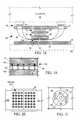
- FIG. 1is a plan view and FIG. 2 is a sectional elevation view of an exemplary prior art probe board assembly 10 for providing signal paths between an integrated circuit tester 12 and ICs 14 formed on a semiconductor wafer 16 .
- Tester 12implements one or more tester channels, each providing a test signal as input to one of ICs 14 or receiving and processing an IC output signal to determine whether the IC output signal is behaving as expected.
- Probe card assembly 10includes a set of pogo pin connectors 26 and a set of three interconnected substrate layers including an interface board 20 , an interposer 22 and a space transformer 24 .
- Pogo pins 28provide signal paths between tester 12 and contact pads 30 on the upper surface of interface board 20 .
- Interface board 20is typically a multiple layer printed circuit board including microstrip and stripline traces for conveying signals horizontally and vias for conveying signals vertically between pads 30 on its planar upper surface and a set of contact pads 32 on its planar lower surface.
- Interposer 22includes one set of spring contacts 34 mounted on its upper surface and a corresponding set of spring contacts 36 mounted on its lower surface. Each spring contact 34 contacts a separate one of the pads 32 on the lower surface of interface board 20 , and each spring contact 36 contacts one of a set of pads 38 on the upper surface of space transformer 24 . Vias passing through interposer 22 provide signal paths between corresponding pairs of spring contacts 34 and 36 .
- Space transformer 24provides signal paths linking spring contacts 36 to a set of probes 40 arranged to contact I/O, power and ground pads 44 on the surfaces of a set of ICs 14 to be tested.
- a chuck 42positions wafer 16 with probes 40 in alignment with IC pads 44 of the ICs 14 to be tested. After one group of ICs 14 have been tested, chuck 42 repositions wafer 16 so that probes 40 access the IC pads 44 of a next group of ICs to be tested.
- probes 40can be implemented as spring contacts formed on the lower surface of space transformer 24 with their tips extending downward to contact IC pads 44 on the surfaces of ICs 14 .
- spring contact type probes 40are attached to the IC's pads 44 with their tips extending upward to contact pads on the lower surface of space transformer 24 .
- a test signal generated by a tester channel implemented within one of circuit boards 18travels through a pogo pin 28 to one of pads 30 on the surface of interface board 20 , and then travels through traces and vias within interface board 20 to one of pads 32 on its lower surface.
- the test signalthen passes through one of spring contacts 34 , through a via within interposer 22 , and through one of spring contacts 36 to one of contacts 38 on the surface of space transformer 24 .
- Traces and vias within space transformer 24then deliver the test signal to a probe 40 which then conveys the test signal to an IC pad 44 on the surface of one of ICs 14 .
- An IC output signal produced at one of IC pads 44follows a similar path in an opposite direction to reach a channel within one of circuit boards 18 .
- interposer 22With its flexible spring contacts 34 and 36 , provides compliant electrical connections between interface board 20 and space transformer 24 .
- Probes 40may be made sufficiently resilient to compensate for any variation in elevation of the IC pads 44 on the upper surfaces of ICs 14 .
- FIG. 2has an expanded vertical scale to more clearly show the various components of probe board assembly 10 .
- the horizontal area over which pogo pins 28 are actually distributedis typically many times larger than the area over which probes 40 are distributed.
- Probe card assembly 10is well adapted for connecting I/O ports of tester channels that are distributed over a relatively wide horizontal area to a set of probes 40 that are aligned to access IC pads 44 that are densely packed into a relatively small horizontal area.
- One problem probe board assembly 10shares to some degree with any interconnect system, is that the signal paths it provides tend to distort and attenuate signals, particularly signals having high frequency components. What is needed is a probe board assembly for providing signal paths between an IC tester and pads on one or more ICs, wherein at least some of the IC pads transmit and receive high frequency signals.
- a system for providing signal paths between an integrated circuit (IC) tester and input/output (I/O), power and ground pads of ICs to be testedincludes a probe board assembly, a flex cable and a set of probes arranged to contact the IC's pads.
- the probe board assemblyincludes one or more substrate layers (which may be rigid) and signal paths through the substrate layer(s) for linking the tester to one set of the probes.
- the flex cableincludes a flexible substrate structurally linked to a layer of the probe board assembly and a set of signal paths through the flexible substrate for linking the tester to another set of the probes.
- FIG. 1is a plan view of a prior art probe board assembly for providing signal paths between an integrated circuit (IC) tester and input/output, power and ground pads on an array of ICs,
- ICintegrated circuit
- FIG. 2is a sectional elevation view of the prior art probe board assembly of FIG. 1 ,
- FIG. 3is a plan view of a probe system in accordance with an exemplary embodiment of the invention for providing signal paths between an IC tester and pads on one or more ICs,
- FIGS. 4 and 5are sectional elevation views the probe system of FIG. 3 .
- FIG. 6is a plan view of the flex cable termination block of FIG. 5 .
- FIG. 7is a plan view of the lower surface of the space transformer of the probe system of FIG. 3 .
- FIG. 8is a sectional elevation view of a probe system in accordance with a second exemplary embodiment of the invention for providing signal paths between an IC tester and pads on one or more ICs,
- FIG. 9is an expanded partial sectional elevation view of the probe system of FIG. 8 .
- FIG. 10is a plan view of the lower surface of the space transformer of the probe system of FIG. 8 .
- FIG. 11is a plan view of the lower surface of a space transformer of a third exemplary embodiment of the invention for providing signal paths between an IC tester and pads on one or more ICs,
- FIG. 12is an expanded partial sectional elevation view of the probe system of FIG. 11 .
- FIG. 13is a sectional elevation view of a probe system in accordance with a fourth exemplary embodiment of the invention for providing signal paths between an IC tester and pads on one or more ICs,
- FIG. 14is a sectional elevation view of a probe system in accordance with a fifth exemplary embodiment of the invention for providing signal paths between an IC tester and IC pads on one or more ICs,
- FIG. 15is an expanded partial sectional elevation view of the probe system of FIG. 14 .
- FIG. 16is a plan view of the lower surface of the space transformer and the flex cables of the probe system of FIG. 14 .
- FIG. 17is an expanded plan view of an area of flex cable of FIG. 16 containing a single substrate island
- FIG. 18is a sectional elevation view of a probe system in accordance with a sixth exemplary embodiment of the invention for providing signal paths between an IC tester and spring contacts formed on pads on one or more ICs,
- FIG. 19is an expanded partial sectional elevation view of the probe system of FIG. 17 .
- FIG. 20is a plan view of the lower surface of the space transformer and the flex cables of the probe system of FIG. 17 ,
- FIG. 21is an expanded plan view of an area of flex cable of FIG. 20 containing a single substrate island
- FIG. 22Ais a side elevation view of a probe system in accordance with a seventh exemplary embodiment of the invention for providing signal paths between an IC tester, remote test equipment and pads on one or more ICs,
- FIG. 22Bis a block diagram illustrating signal paths within the flex cable of FIG. 22A .
- FIG. 23Ais a plan view of a probe system in accordance with an eighth exemplary embodiment of the invention.
- FIG. 23Bis a side elevation view of the probe system of FIG. 23A .
- FIGS. 24A-24Gillustrate steps in an exemplary embodiment of a process for forming probe tips on a flex cable in accordance with the invention.
- the present inventionis directed to a probe board assembly for providing signal paths between an integrated circuit (IC) tester and input/output (I/O), power and ground pads of one or more ICs to be tested either while the ICs are still in the form of die on a semiconductor wafer or after they have been separated from one another.
- ICintegrated circuit
- I/Oinput/output
- the specificationdescribes exemplary embodiments and applications of the invention considered by the applicant(s) to be the best modes of practicing the invention. It is not intended, however, that the invention be limited to the exemplary embodiments described below or to the particular manner in which the embodiments operate.
- FIG. 3is a plan view and FIGS. 4 and 5 are sectional elevation views of a probe system 50 in accordance with an exemplary embodiment of the invention for providing signal paths between an IC tester 52 to I/O, power and ground pads 54 on the surfaces of ICs 56 , for example, while still in the form of die on a semiconductor wafer 58 .
- Vertical dimensions in FIGS. 4 and 5are exaggerated so that the individual components forming probe system 50 may be more easily distinguished.
- Probe system 50includes a probe board assembly 51 having multiple interconnected substrate layers, including an interface board 60 , an interposer 62 and a space transformer 64 .
- Pogo pin connectors 66 within IC tester 52include a set of pogo pins 68 providing signal paths between the tester 52 and contact pads 70 residing in on the upper surface of interface board 60 .
- Interface board 60preferably, though not exclusively, comprises one or more layers of rigid insulating substrate material upon which are formed microstrip and/or stripline traces for conveying signals horizontally and through which are provided vias for conveying signals vertically between the pads 70 on its upper surface and a set of contact pads 72 on its lower surface.
- Interposer 62preferably, though not exclusively, includes a rigid insulating substrate having a set of flexible spring contacts 74 mounted on its upper surface and a corresponding set of flexible spring contacts 76 mounted on its lower surface. Each spring contact 74 contacts a separate one of the pads 72 on the lower surface of interface board 60 , and each spring contact 76 contacts one of a set of pads 78 on the upper surface of space transformer 64 . A set of conductive vias passing though interposer 62 provide signal paths between corresponding pairs of spring contacts 74 and 76 .
- Space transformer 64provides signal paths linking the pads 78 on its upper surface to a set of probes 80 arranged to contact IC pads 54 on the surfaces of a set of ICs 56 to be tested.
- Wafer 58resides on a chuck 82 for positioning wafer 58 so that probes 80 contact the pads 54 of the ICs 56 to be tested. After one group of ICs 56 have been tested, chuck 82 repositions wafer 56 so that probes 80 access the pads 54 of a next group of ICs 56 to be tested.
- interposer 62With its flexible spring contacts 74 , 76 , provides compliant electrical connections between interface board 60 and space transformer 64 .
- Probes 80may be sufficiently resilient to compensate for any variation in elevation of the pads 54 on the upper surfaces of ICs 56 .
- Various types of structurescan be used to implement probes 80 including, for example, wire bond and lithographic spring contacts, needle probes, and cobra probes.
- Spring contactsmay be formed on a pad or other base structure of a substrate in any of a number of ways.
- a spring contactmay be formed by wire bonding a wire to the pad and overcoating the wire with a resilient material, such as disclosed in U.S. Pat. No. 6,336,269 issued Jan. 8, 2002 to Eldridge et al., incorporated herein by reference.
- a spring contactmay be formed lithographically by depositing material in one or more molds formed over the pad and substrate. Examples of such lithographic techniques can be found in U.S. Pat. No.
- spring contactsWhen spring contacts are employed to implement probes 80 , they can be formed on the pads 54 of ICs 56 when space transformer 64 includes pads 81 on its lower planar surface arranged to contact the tips of the spring contacts. Alternatively, spring contact probes 80 may be formed on the pads 81 on the lower planar surface space transformer 64 and arranged so that their tips contact the pads 54 of ICs 54 .
- U.S. Pat. No. 6,064,213, issued May 16, 2000 to Khandros et al.disclose and example of a card assembly designed to contact spring contacts formed on an IC.
- a test, power or ground signal provided at an I/O port of an IC tester 52travels through one of pogo pins 68 to one of pads 70 on the surface of interface board 60 , and then travels through traces and vias within interface board 60 to one of pads 72 on its lower surface.
- the test signalthen passes through one of spring contacts 74 , through a via within interposer 62 , and through one of spring contacts 76 to one of pads 78 on the surface of space transformer 64 . Traces and vias within space transformer 64 then deliver the test signal to one of probes 80 which forwards the test signal to one of IC pads 54 .
- An IC output signal generated at one of IC pads 54follows a similar path in an opposite direction on its way back to an I/O port of a channel within tester 52 .
- probe system 50provides a signal path between IC tester 52 and IC pads 54 suitable for conveying high frequency signals, for example up to approximately 100 GHz in frequency.
- a pogo pin connector 84 mounted on a lower edge of a printed circuit board within IC tester 52provides pogo pins 83 for conveying high frequency signals between a tester channel I/O port and pads 85 formed on an end of a flex cable 86 linked to conductors within the flex cable. Opposite ends of the conductors within flex cable 86 are terminated on the lower surface of space transformer 64 .
- Flex cable 86includes a flexible substrate holding conductors for conveying signals. Various types of well-known flex cables may be used to implement flex cable 86 .
- flex cable 86may include one or more substrate layers of flexible polyimide, teflon, or other dielectric material upon which microstrip and/or strip-line conductors of copper or other conductive material are formed, for example through lithographic techniques, to provide uniform transmission line environments over the entire length of the flex cable.
- a flex cable 86may provide parallel pairs of traces providing paths for high noise immunity differential signals.
- Flex cable 86may alternatively consist of or include one or more coaxial cables and may include other types of transmission lines formed on or within the flexible substrate for providing signal paths through the flex cable.
- FIGS. 4 and 5employ pogo pin connectors 66 or 84 as signal paths between IC tester 52 and probe board 50
- the signal paths between IC tester 52 and probe board 50may be implemented in many other ways, such as for example through coaxial or flex cables or various types of well-known connectors such as SMB, SMP or SMA connectors.
- an upper end of flex cable 86may be encased in epoxy 90 or other suitable insulating material to form a cable termination block 92 .
- the top of termination block 92may be ground to a flat surface to expose ends of the conductors.
- Conductive material deposited on the exposed conductor endsmay provide pads 85 for receiving pogo pins 83 .
- Each termination block 92is suitably held by adhesive within an opening in interface board 60 with the termination block positioned so that the pads 85 on its upper surface reside in same plane on the upper surface of the interface board as pads 70 (FIG. 4 ).
- FIG. 7is an upward-directed plan view of the lower surface of space transformer 64 upon which four flex cables 86 are terminated.
- space transformer 64is depicted as having an array of 36 probe pads 81 on its under surface upon which probes 80 ( FIG. 5 ) may be formed, though in practice space transformer 64 may include a much larger array of pads 81 .
- Exposed lower ends 94 of the conductors provided by flex cables 86are connected (as by solder, wire bonds, conductive adhesive, or other means) to pads 96 on the lower surface of space transformer 64 .
- Traces 98 formed on the lower surface of space transformer 64link some of pads 96 to some of probe pads 81 .
- Upward extending viasmay link other conductors 94 to traces (not shown) formed on higher layers of space transformer 64 .
- the higher layer tracesextend to other vias (not shown) passing downward to other probe pads 81 .
- a signal path between tester 52 and spring contacts 80 provided by pogo pins 83 and flex cable 86 of FIG. 5can have a higher bandwidth than a signal path passing through probe board assembly 51 because most of the higher bandwidth path consists of a highly uniform transmission line environment having evenly distributed impedance. Also the higher bandwidth path includes substantially fewer junctions between dissimilar transmission lines that can cause signal attenuation and distortion. As described above, a signal path through pogo pins 66 (FIG. 4 ), interface board 60 , interposer 62 and space transformer 64 may include 10 or more such junctions. A signal path though pogo pins 83 (FIG. 5 ), flex cable 86 , and traces 96 ( FIG. 7 ) on the lower surface of space transformer 64 includes only three transmission line junctions.
- FIGS. 8-10illustrate another example probe system 100 having much in common with probe system 50 of FIGS. 3-5 and, accordingly, similar reference characters refer to similar structures.
- probe system 100differs from probe board assembly 51 not only because it employs two flex cables 86 instead of four, but also because the lower ends of the conductors within flex cables 86 are coupled to IC pads 54 in a way that bypasses spring contacts 80 .
- flex cable 86includes serpentine substrate fingers 102 containing conductors forming signal paths extending into the area under space transformer 64 occupied by probes 80 . Bypassing various probes 80 A carrying signals between space transformer 64 and various IC pads 54 A, each finger 102 extends over one or more IC pads 54 B that are to transmit or receive high frequency signals via the transmission line(s) included in the finger. Pointed conductive tips 106 formed on the underside of fingers 102 act as probes to provide signal paths between the transmission lines residing within the fingers and the high frequency IC pads 54 B.
- spring contacts 80 Bthat are somewhat shorter than the spring contacts 80 A that carry lower frequency signals to and from IC pads 54 A are bonded to the upper surfaces of flex cable fingers 102 to structurally link each finger 102 to the under surface of space transformer 64 .
- Spring contacts 80 Bdo not carry signals but instead act as flexible structural member for holding fingers 102 in place under space transformer 64 so that their tips 106 , and restricting their range of motion relative to the space transformer so that they are properly aligned with IC pads 54 B.
- the uniform transmission line environments provided by conductors within flex cables 86extend from pogo pins 83 all the way down to the tips 106 acting as probes to contact IC pads 54 B.
- the flex cable termination arrangement of probe system 100eliminates probe 80 and signal paths within space transformer 64 needed by the cable termination arrangement of probe system 50 of FIGS. 5-7 and therefor reduces the number of transmission line junctions in the signal path.
- ICs 56may warm up and expand while they are being tested and thereby may cause IC pads 54 to move vertically and to move apart horizontally.
- Fingers 102are flexible so that tips 106 can move vertically as necessary to allow them to remain in contact with IC pads 54 B.
- Fingers 102preferably extend in a serpentine manner under space transformer 64 as illustrated in FIG. 10 to provide them with longitudinal flexibility to permit tips 54 B to move horizontally relative to one another as necessary to remain in contact with IC pads 54 B.
- Space transformer 64is preferably formed of a ceramic or other substrate material having a coefficient of thermal expansion similar to that of the semiconductor material forming wafer 58 . The temperature of space transformer 64 tends to track that of wafer 58 since it is positioned very close to the wafer.
- probes 80tend to move apart at the same rate as IC pads 54 A so that probes 80 remain in contact with IC pads 54 A. Since the serpentine flex cable fingers 102 have the flexibility to move in the horizontal plane parallel to the plane of the wafer, and since spring contacts 80 B attached to finger 102 above finger tips 54 structurally link fingers 102 to space transformer 64 , finger tips 54 also move in a vertical direction perpendicular to the plane of the wafer surface as necessary to remain in contact with pads 54 B as pads 54 B move apart with increasing wafer temperature.
- FIGS. 11 and 12illustrate another exemplary embodiment of the invention employing an alternative approach for terminating conductors of the flex cables of probe system 100 under space transformer 64 .
- FIG. 11an upward-directed plan view of the undersides of flex cables 86 having fingers 120 extending under space transformer 64 .
- FIG. 12is a partial sectional elevation view of one finger 120 extending between space transformer 64 and an IC 56 . Fingers 120 extend over the IC pads 54 B that are to be accessed by conductors within fingers 120 . Tips 106 on the underside of fingers 120 provide signal paths between I/O pads 54 B and the conductors within fingers 120 . Probes 80 B connected between fingers 120 and pads 81 on the under surface of space transformer 64 do not carry signals, but instead act only as flexible structural members supporting fingers 120 and restricting their range of horizontal motion.
- fingers 120may pass over some contacts 54 C that are to be accessed via spring contacts 80 C attached to and extending downward from pads 81 on the underside of space transformer 64 .
- Lower ends of spring contacts 80 Care attached to upper surfaces of vias 122 extending vertically though flex cable fingers 120 to tips 124 mounted on the under surface of flex cable 86 for contacting IC pads 54 C.
- Lower frequency signalsmay therefore pass between IC pads 54 C and pads 81 on the lower surface of space transformer 64 through probes 80 C, vias 122 and probe tips 124 while higher frequency signals entering or departing IC pads 54 B pass through probe tips 106 and conductors implemented within flex cable fingers 120 .
- Lower frequency signalsmay also pass between pads 81 and IC pads 54 A directly through probes 80 A.
- FIG. 13is a sectional elevation view of a probe system 110 in accordance with another exemplary embodiment of the invention that is a variation on probe system 50 of FIG. 5 , wherein similar reference characters refer to similar structures.
- Probe board assembly 110differs from probe board assembly 50 in that upper ends of conductors within flex cables 86 are terminated on pads 112 formed on the lower surface of interface board 60 . Traces and vias (not shown) formed on and within interface board 60 link pads 112 to the pads 85 on the upper surface of the interface board contacted by pogo pins 83 .
- FIG. 14is a sectional elevation view of a probe system 120 in accordance with another exemplary embodiment of the invention that is a variation on probe system 100 of FIG. 8 , wherein similar reference characters refer to similar structures.
- FIG. 15is an expanded sectional elevation view of the portion of the probe system 120 of FIG. 14 residing between space transformer 64 and ICs 56
- FIG. 16is a plan view looking upward from of wafer 58 toward the under sides of flex cables 86 and space transformer 64 .
- Probe system 120 of FIG. 14differs from probe system 100 in that flex cables 86 extend completely under space transformer 64 as best seen in FIGS. 15 and 16 .
- Probe tips 130 mounted on the lower sides of flex cables 86contact the IC pads 54 .
- Flexible spring contacts 80 attached between pads 81 on the lower surface of space transformer 64 and to pads 132 on the upper surfaces of flex cables 86 above probe tips 130provide support for cables 86 .
- Vias 133 through flex cables 86may link one set of probe tips 130 to the pads 132 above the tips.
- IC tester 52is therefore able to communicate with some IC pads 56 by way of paths extending through probe board 60 , interposer 62 , space transformer 64 , spring contacts 80 , vias 133 and probe tips 130 .
- a second set of probe tips 130 formed on the lower surface of flex cables 86are connected to the signal paths (not shown) provided by flex cable 86 so that IC tester 52 may also communicate with some of IC pads 54 through high frequency signals passing through flex cables 86 and probe tips 130 .
- the spring contacts 80 above the second set of probe tips 130do not convey signals, but they do provide flexible support for the probe tips.
- FIG. 17is an enlarged plan view of area of flex cable 86 holding one of probe tips 130 .
- Parts of the substrate material of flex cable 86are removed to create spaces 134 nearly surrounding an island 138 of flex cable substrate holding probe tip 130 .
- Two (or more) small, flexible serpentine bridges 140 of flex cable substrateremain to link each substrate island 138 to the main expanse of flex cable 86 .
- those signal pathsextend to that set of probe tips 130 through bridges 140 .
- Bridges 140 and the spring contacts 80 connected to flex cable 86 above islands 138also hold tips 130 in position above the IC pads 54 ( FIG. 13 ) they contact.
- IC pads 54are not perfectly co-planar with one another, and they can move both vertically and horizontally as the ICs under test warm up and expand.
- Bridges 140 and the spring contact 80 above each probe tip 130have sufficient flexibility to allow the probe tip 130 to move vertically as necessary to remain in contact an IC pad 54 even though the elevation of the pad may change as the IC wafer begins to warm up.
- the serpentine nature of bridges 140provides them with sufficient flexibility to allow probe tips 130 to also move horizontally relative to one another and relative to the main body of flex cable 86 as necessary to remain in contact with the IC pads 54 when the pads move horizontally during thermal expansion of the ICs under test.
- FIG. 18is a sectional elevation view of a probe system 150 in accordance with another exemplary embodiment of the invention that is a variation on probe system 110 of FIG. 14 , wherein similar reference characters refer to similar structures.
- FIG. 19is an expanded sectional elevation view of the portion of the probe system 150 of FIG. 18 residing between space transformer 64 and ICs 56
- FIG. 20is a plan view looking upward from wafer 58 toward the under sides of flex cables 86 and space transformer 64
- FIG. 20is an enlarged view of a portion of the flex cable 86 of FIG. 20 illustrating a single substrate island 138 linked to flex cable 86 thorough substrate bridges 140 .
- Probe system 150provides signal paths between IC tester of FIG. 18 and spring contacts 152 that are attached to the pads 54 of ICs 56 .
- Probe system 150differs from probe system 110 of FIG. 14 in that in probe system 150 pads 154 on the upper surface of flex cable substrate islands 138 are directly connected by a solder ball array 156 to pads 81 on the lower surface of space transformer 64 . Also a pad 158 , rather than a probe tip, is formed on the lower surface of each flex cable substrate island 138 . Pads 158 are positioned so that they may be contacted by tips of the spring contacts 152 extending upward from the IC pads 54 .
- IC tester 52is therefore able to communicate with some IC pads 56 by way of paths extending through probe board 60 , interposer 62 , space transformer 64 , solder balls 156 vias 133 , pads 158 and spring contacts 152 .
- a second set of pads 158 formed on the lower surfaces of substrate islands 138are connected to the signal paths (not shown) provided by flex cable 86 so that IC tester 52 may also communicate with some of IC pads 54 through high frequency signals passing through flex cables 86 , substrate bridges 140 , pads 158 and spring contacts 152 .
- FIG. 22Aillustrates another exemplary embodiment of the invention, a multiple-layer probe card assembly 160 for providing signal paths between an integrated circuit tester 162 and pads 163 on surfaces of IC dice 164 on a wafer 166 under test. Probe assembly 160 can also provide remote test equipment (not shown) with signal access to IC pads 163 .
- Probe card assembly 160includes a probe board 170 having a set of pads 172 on its upper surface for receiving tips of a set of pogo pin connectors 174 providing signal paths between tester 162 and pads 172 .
- Signal paths extending through one or more flex cables 175interconnect a set of spring contacts 176 and 178 formed on the upper and lower surfaces of flex cable 175 provide signal paths between a set of pads 180 on the lower surface of probe board 170 and a set of pads 182 on an upper surface of a space transformer board 184 .
- a set of probes 186provide signal paths between pads 188 on the lower surface of space transformer 184 and IC pads 163 .
- Probe board 170 and space transformer 184may include single or multiple insulating substrate layers, traces formed on the substrate layers, and vias extending through the substrate layers for conducting signals horizontally and vertically between pads and/or contacts on their upper and lower surfaces.
- Some of spring contacts 178may contact signal paths within flex cables 175 that may extend to probe board 170 .
- Probe board 170links some of its upper surface contacts 172 to the conductors within the flex cable 175 , thereby permitting high frequency or other signals traveling via flex cable 175 to spring contacts 178 and to by-pass transmission line junctions within probe board 170 and between pads 180 and contacts 176 .
- One or more conductors of flex cableS 175may extend to remote equipment (not shown) connected anywhere by any means to a rigid substrate.)
- FIG. 22Bis a block diagram illustrating an exemplary signal routing scheme within flex cable 175 .
- a flex cableincludes a flexible substrate that can be used like a circuit board to hold install small surface mounted devices on a flex cable, including passive devices such as resistors and capacitors and active devices including, for example, integrated circuit switches, multiplexers and the like which can act a signal routing devices.
- FIG. 22Bshows a set of integrated circuit routing switches 191 powered and controlled by signals from one of tester channels for selectively linking the pads 192 on the lower surface of flex cable 175 accessed by spring contacts 178 of FIG. 22A to various other conductors including spring contacts 176 and flex cable conductors leading to tester 162 or to the remote equipment.
- the switching arrangement of FIG. 22Bis useful, for example, when IC tester 162 and other remote test equipment carry out different types of tests at the IC terminals.
- IC tester 162may be adapted to carry out logic tests on ICs 164 while the remote equipment may be adapted to carry out parametric tests on the ICs.
- the remote equipmentmay also supply the power for the ICs being tested.
- Some paths to the remote equipment(such as for example those connected to power supplies) may connect directly to spring contacts 178 so that remote equipment and tester 162 can concurrently access various IC pins during a test.
- more then one IC tester of the same typecan concurrently access the ICs.
- routing switches 191are not needed since each flex cable conductor and each spring contact 176 accesses a separate spring contact 179 .
- the flex cables 175can be easily replaced with flex cables have different signal routing arrangements to accommodate changes in routing patterns resulting in changes to the ICs being tested or to accommodate changes in the test equipment.
- FIG. 23Ais a plan view, of a pair of flex cables 86 passing under a rigid substrate 193 looking upward from a wafer 194 ( FIG. 23B ) being accessed via a set of probes 195 attached either to space transform 193 or to pads on the surface of wafer 194 .
- Probes 195pass through a set of windows 196 in flex cables 86 .
- FIG. 23Bis a sectional elevation view along cut line B—B of FIG. 23 A.
- FIGS. 23A and 23Billustrate an alternative approach to linking some of probes 156 to conductors 197 in flex cable 86 .
- a set of spring contacts 198extending between pads on the upper surface of flex cable 86 linked to conductors 197 through vias 199 passing vertically through flex cable 86 and pads 200 on the lower surface of substrate 193 .
- This type of interconnect arrangementcan be employed in lieu of or in addition to the interconnect arrangements illustrated in FIGS. 7 , 10 , 11 , 15 and 19 .
- FIGS. 24A-24Gillustrate an exemplary process for forming contact tip structures and attaching them to pads of a flex cable so that the cables may be employed in various exemplary embodiments of the invention described herein above.
- a set of pits 210are suitably formed in a substrate 212 of any suitable material such as, for example, a silicon semiconductor wafer using photolithographic etching or any other suitable technique.
- 24C masking material 216such as photoresist is then deposited on the releasing/shorting material 214 to form a set of molds 218 defining shapes of the contact tip structures.
- conductive material 220 that is to form the contact tip structuresis then deposited in the molds.
- the tip structure material 220may be deposited by electroplating or any other known process of depositing material within a pattern masking material.
- the masking material 216is then removed to reveal a set of tips 222 .
- the tip structures 222are then attached to pads 224 on the flex cable 226 using joining material 228 such as, for example, conductive adhesive, solder, brazing material and the like.
- the release/shorting layer 218is then removed, for example by etching, to release the tip structures 230 from substrate 210 shown in FIG. 24 G.
- Releasing/shorting layer 214thus not only facilitates the formation of tips 222 though electroplating, it also provides a base for tips 222 which can be easily etched to release tips 22 from substrate 210 .
- Releasing/shorting layer 214may include one or more layers, with a releasing material layer being formed first and a shorting material layer being formed on the releasing material layer.
- tip structure 230 shown in FIG. 24Gis not critical to the invention and other suitable tip structures of various sizes and shapes can be formed in a similar manner. Additional exemplary tip structures are disclosed in U.S. patent application Ser. No. 08/819,464, filed Mar. 17, 1997, now abandoned, and U.S. patent application Ser. No. 09/189,761, filed Nov. 10, 1998, both incorporated herein by reference.
- FIGS. 7 , 10 , 11 and 15illustrate exemplary embodiments of the invention employing two or four flex cables 86 , it should be understood that the number of flex cables and the number of conductors included in each flex cable can be chosen to suit the requirements of each particular test interconnect application. While pogo pin connectors 66 or 84 ( FIGS.
- FIGS. 4 , 8 , 13 or 14may be used to link flex cables 86 or interface board 60 to tester 52 , other types of connectors known to those of skill in the art may be employed.
- the probe board assemblies illustrated in FIGS. 4 , 8 , 13 and 14are exemplary and may be implemented using more or fewer interconnected substrate layers.
- the interposer 62 shown in FIGS. 5 , 8 , 13 , 14 and 18may be eliminated and the space transfer 64 connected directly to interface board 60 .
- interposer 62 and space transformer 64 of those figuresmay be eliminated when probes 80 are formed directly on interface board 60 .
- the suggested signal frequency ranges for the various types of signal paths through the probe board assembly and flex cableare exemplary and not intended to be limiting.
Landscapes
- Physics & Mathematics (AREA)
- General Physics & Mathematics (AREA)
- Engineering & Computer Science (AREA)
- Computer Hardware Design (AREA)
- Microelectronics & Electronic Packaging (AREA)
- General Engineering & Computer Science (AREA)
- Measuring Leads Or Probes (AREA)
- Testing Or Measuring Of Semiconductors Or The Like (AREA)
Abstract
Description
Claims (52)
Priority Applications (13)
| Application Number | Priority Date | Filing Date | Title |
|---|---|---|---|
| US10/142,548US6965244B2 (en) | 2002-05-08 | 2002-05-08 | High performance probe system |
| US10/430,628US6911835B2 (en) | 2002-05-08 | 2003-05-05 | High performance probe system |
| CNA038103974ACN1653340A (en) | 2002-05-08 | 2003-05-07 | High peformance probe system for testing semiconductor wafers |
| TW092112478ATWI266882B (en) | 2002-05-08 | 2003-05-07 | High performance probe system |
| EP03736564AEP1506414A2 (en) | 2002-05-08 | 2003-05-07 | High peformance probe system for testing semiconductor wafers |
| KR1020047017779AKR100997923B1 (en) | 2002-05-08 | 2003-05-07 | High performance probe systems |
| AU2003237195AAU2003237195A1 (en) | 2002-05-08 | 2003-05-07 | High performance probe system for testing semiconductor wafers |
| PCT/US2003/014490WO2003100446A2 (en) | 2002-05-08 | 2003-05-07 | High performance probe system for testing semiconductor wafers |
| JP2004507852AJP4688095B2 (en) | 2002-05-08 | 2003-05-07 | High performance probe system for testing semiconductor wafers |
| US11/273,889US7227371B2 (en) | 2002-05-08 | 2005-11-14 | High performance probe system |
| US11/758,525US7443181B2 (en) | 2002-05-08 | 2007-06-05 | High performance probe system |
| US12/259,785US7764075B2 (en) | 2002-05-08 | 2008-10-28 | High performance probe system |
| US12/844,126US8614590B2 (en) | 2002-05-08 | 2010-07-27 | High performance probe system |
Applications Claiming Priority (1)
| Application Number | Priority Date | Filing Date | Title |
|---|---|---|---|
| US10/142,548US6965244B2 (en) | 2002-05-08 | 2002-05-08 | High performance probe system |
Related Child Applications (3)
| Application Number | Title | Priority Date | Filing Date |
|---|---|---|---|
| US10/430,628Continuation-In-PartUS6911835B2 (en) | 2002-05-08 | 2003-05-05 | High performance probe system |
| US11/273,889DivisionUS7227371B2 (en) | 2002-05-08 | 2005-11-14 | High performance probe system |
| US11/273,889ContinuationUS7227371B2 (en) | 2002-05-08 | 2005-11-14 | High performance probe system |
Publications (2)
| Publication Number | Publication Date |
|---|---|
| US20040036493A1 US20040036493A1 (en) | 2004-02-26 |
| US6965244B2true US6965244B2 (en) | 2005-11-15 |
Family
ID=31886331
Family Applications (5)
| Application Number | Title | Priority Date | Filing Date |
|---|---|---|---|
| US10/142,548Expired - LifetimeUS6965244B2 (en) | 2002-05-08 | 2002-05-08 | High performance probe system |
| US11/273,889Expired - LifetimeUS7227371B2 (en) | 2002-05-08 | 2005-11-14 | High performance probe system |
| US11/758,525Expired - LifetimeUS7443181B2 (en) | 2002-05-08 | 2007-06-05 | High performance probe system |
| US12/259,785Expired - Fee RelatedUS7764075B2 (en) | 2002-05-08 | 2008-10-28 | High performance probe system |
| US12/844,126Expired - LifetimeUS8614590B2 (en) | 2002-05-08 | 2010-07-27 | High performance probe system |
Family Applications After (4)
| Application Number | Title | Priority Date | Filing Date |
|---|---|---|---|
| US11/273,889Expired - LifetimeUS7227371B2 (en) | 2002-05-08 | 2005-11-14 | High performance probe system |
| US11/758,525Expired - LifetimeUS7443181B2 (en) | 2002-05-08 | 2007-06-05 | High performance probe system |
| US12/259,785Expired - Fee RelatedUS7764075B2 (en) | 2002-05-08 | 2008-10-28 | High performance probe system |
| US12/844,126Expired - LifetimeUS8614590B2 (en) | 2002-05-08 | 2010-07-27 | High performance probe system |
Country Status (1)
| Country | Link |
|---|---|
| US (5) | US6965244B2 (en) |
Cited By (37)
| Publication number | Priority date | Publication date | Assignee | Title |
|---|---|---|---|---|
| US20050142739A1 (en)* | 2002-05-07 | 2005-06-30 | Microfabrica Inc. | Probe arrays and method for making |
| US20050156165A1 (en)* | 1997-01-15 | 2005-07-21 | Formfactor, Inc. | Test assembly including a test die for testing a semiconductor product die |
| US20060046529A1 (en)* | 2004-09-02 | 2006-03-02 | Mcknight Samuel R | High density space transformer and method of fabricating same |
| US20060066332A1 (en)* | 2002-05-08 | 2006-03-30 | Formfactor, Inc. | High performance probe system |
| US20060220228A1 (en)* | 2002-12-18 | 2006-10-05 | Micron Technology, Inc. | Methods and apparatus for a flexible circuit interposer |
| US20060281364A1 (en)* | 2005-06-14 | 2006-12-14 | Honeywell International, Inc. | Area array device test adapter |
| US20070075717A1 (en)* | 2005-09-14 | 2007-04-05 | Touchdown Technologies, Inc. | Lateral interposer contact design and probe card assembly |
| US20070090847A1 (en)* | 2005-10-20 | 2007-04-26 | Mjc Probe Incorporation | Stepped PCB for probe card, probe card having the same and method for clamping the probe card |
| US20080001617A1 (en)* | 2006-06-09 | 2008-01-03 | Octavian Scientific, Inc, | Method and apparatus for fixed-form multi-planar extension of electrical conductors beyond the margins of a substrate |
| US20080180121A1 (en)* | 1993-11-16 | 2008-07-31 | Formfactor, Inc. | Probe card assembly and kit |
| US20090160432A1 (en)* | 2005-07-08 | 2009-06-25 | Formfactor, Inc. | Probe card assembly with an interchangeable probe insert |
| US7944224B2 (en) | 2005-12-07 | 2011-05-17 | Microprobe, Inc. | Low profile probe having improved mechanical scrub and reduced contact inductance |
| US7952377B2 (en) | 2007-04-10 | 2011-05-31 | Microprobe, Inc. | Vertical probe array arranged to provide space transformation |
| US8111080B2 (en) | 2004-05-21 | 2012-02-07 | Microprobe, Inc. | Knee probe having reduced thickness section for control of scrub motion |
| US8203353B2 (en) | 2004-07-09 | 2012-06-19 | Microprobe, Inc. | Probes with offset arm and suspension structure |
| USRE43503E1 (en) | 2006-06-29 | 2012-07-10 | Microprobe, Inc. | Probe skates for electrical testing of convex pad topologies |
| US8230593B2 (en) | 2008-05-29 | 2012-07-31 | Microprobe, Inc. | Probe bonding method having improved control of bonding material |
| USRE44407E1 (en) | 2006-03-20 | 2013-08-06 | Formfactor, Inc. | Space transformers employing wire bonds for interconnections with fine pitch contacts |
| US8723546B2 (en) | 2007-10-19 | 2014-05-13 | Microprobe, Inc. | Vertical guided layered probe |
| US8907689B2 (en) | 2006-10-11 | 2014-12-09 | Microprobe, Inc. | Probe retention arrangement |
| US8988091B2 (en) | 2004-05-21 | 2015-03-24 | Microprobe, Inc. | Multiple contact probes |
| US9097740B2 (en) | 2004-05-21 | 2015-08-04 | Formfactor, Inc. | Layered probes with core |
| US9435855B2 (en) | 2013-11-19 | 2016-09-06 | Teradyne, Inc. | Interconnect for transmitting signals between a device and a tester |
| US9476911B2 (en) | 2004-05-21 | 2016-10-25 | Microprobe, Inc. | Probes with high current carrying capability and laser machining methods |
| US9594114B2 (en) | 2014-06-26 | 2017-03-14 | Teradyne, Inc. | Structure for transmitting signals in an application space between a device under test and test electronics |
| US20170117198A1 (en)* | 2015-10-21 | 2017-04-27 | Joung-yeal Kim | Semiconductor device and semiconductor package comprising the same |
| US9977052B2 (en) | 2016-10-04 | 2018-05-22 | Teradyne, Inc. | Test fixture |
| US10120020B2 (en) | 2016-06-16 | 2018-11-06 | Formfactor Beaverton, Inc. | Probe head assemblies and probe systems for testing integrated circuit devices |
| US10416192B2 (en) | 2003-02-04 | 2019-09-17 | Microfabrica Inc. | Cantilever microprobes for contacting electronic components |
| US10677815B2 (en) | 2018-06-08 | 2020-06-09 | Teradyne, Inc. | Test system having distributed resources |
| US11067658B2 (en)* | 2018-09-13 | 2021-07-20 | Samsung Electronics Co., Ltd. | Probe card inspection wafer, probe card inspection system, and method of inspecting probe card |
| US11262383B1 (en) | 2018-09-26 | 2022-03-01 | Microfabrica Inc. | Probes having improved mechanical and/or electrical properties for making contact between electronic circuit elements and methods for making |
| US11363746B2 (en) | 2019-09-06 | 2022-06-14 | Teradyne, Inc. | EMI shielding for a signal trace |
| US11821918B1 (en) | 2020-04-24 | 2023-11-21 | Microfabrica Inc. | Buckling beam probe arrays and methods for making such arrays including forming probes with lateral positions matching guide plate hole positions |
| US11828775B1 (en) | 2020-05-13 | 2023-11-28 | Microfabrica Inc. | Vertical probe arrays and improved methods for making using temporary or permanent alignment structures for setting or maintaining probe-to-probe relationships |
| US11862901B2 (en) | 2020-12-15 | 2024-01-02 | Teradyne, Inc. | Interposer |
| US20240329085A1 (en)* | 2021-07-28 | 2024-10-03 | Yokowo Co., Ltd. | Probe card |
Families Citing this family (42)
| Publication number | Priority date | Publication date | Assignee | Title |
|---|---|---|---|---|
| US6911835B2 (en)* | 2002-05-08 | 2005-06-28 | Formfactor, Inc. | High performance probe system |
| JP2007024582A (en)* | 2005-07-13 | 2007-02-01 | Agilent Technol Inc | Display panel inspection device and interface used therefor |
| US7352602B2 (en)* | 2005-12-30 | 2008-04-01 | Micron Technology, Inc. | Configurable inputs and outputs for memory stacking system and method |
| TWI600099B (en)* | 2006-07-07 | 2017-09-21 | 川斯拉利特公司 | Methods and apparatus for planar extension of electrical conductors beyond the edges of a substrate |
| US7749778B2 (en)* | 2007-01-03 | 2010-07-06 | International Business Machines Corporation | Addressable hierarchical metal wire test methodology |
| US7580296B2 (en)* | 2007-03-30 | 2009-08-25 | Sandisk 3D Llc | Load management for memory device |
| CA2592901C (en)* | 2007-07-13 | 2012-03-27 | Martin Blouin | Semi-generic in-circuit test fixture |
| KR100998762B1 (en) | 2008-08-25 | 2010-12-07 | 주식회사 코리아 인스트루먼트 | Probe card |
| US8134380B2 (en)* | 2008-11-26 | 2012-03-13 | Taiwan Semiconductor Manufacturing Company, Ltd. | Test probe structure |
| US8073019B2 (en)* | 2009-03-02 | 2011-12-06 | Jian Liu | 810 nm ultra-short pulsed fiber laser |
| JP5379065B2 (en) | 2010-04-21 | 2013-12-25 | 新光電気工業株式会社 | Probe card and manufacturing method thereof |
| US8564319B2 (en) | 2010-06-17 | 2013-10-22 | Taiwan Semiconductor Manufacturing Company, Ltd. | Probe card for simultaneously testing multiple dies |
| US9054632B2 (en)* | 2010-08-06 | 2015-06-09 | First Solar, Inc. | In-process electrical connector |
| US8878560B2 (en)* | 2010-12-30 | 2014-11-04 | Taiwan Semiconductor Manufacturing Company, Ltd. | High frequency probing structure |
| US9244099B2 (en)* | 2011-05-09 | 2016-01-26 | Cascade Microtech, Inc. | Probe head assemblies, components thereof, test systems including the same, and methods of operating the same |
| US10776233B2 (en) | 2011-10-28 | 2020-09-15 | Teradyne, Inc. | Programmable test instrument |
| US9470759B2 (en)* | 2011-10-28 | 2016-10-18 | Teradyne, Inc. | Test instrument having a configurable interface |
| US9759772B2 (en) | 2011-10-28 | 2017-09-12 | Teradyne, Inc. | Programmable test instrument |
| US9974187B2 (en) | 2013-04-22 | 2018-05-15 | Infineon Technologies Austria Ag | Power in lead |
| US9372205B2 (en)* | 2014-01-15 | 2016-06-21 | Taiwan Semiconductor Manufacturing Co., Ltd. | Universal probe card PCB design |
| US10088503B2 (en)* | 2014-02-27 | 2018-10-02 | Taiwan Semiconductor Manufacturing Co., Ltd. | Probe card |
| US10096958B2 (en)* | 2015-09-24 | 2018-10-09 | Spire Manufacturing Inc. | Interface apparatus for semiconductor testing and method of manufacturing same |
| IT201700017061A1 (en)* | 2017-02-15 | 2018-08-15 | Technoprobe Spa | Improved measurement card for high frequency applications |
| IT201700017037A1 (en)* | 2017-02-15 | 2018-08-15 | Technoprobe Spa | Measurement board for high frequency applications |
| IT201800006903A1 (en)* | 2018-07-04 | 2020-01-04 | Measurement board for high frequency applications | |
| TW202501920A (en) | 2018-07-20 | 2025-01-01 | 美商Fci美國有限責任公司 | Connector, connector assembly, interconnection system and method of operating the same |
| CN113491035B (en) | 2019-01-14 | 2024-06-14 | 安费诺有限公司 | Middle plate cable termination assembly |
| TWI861044B (en) | 2019-01-14 | 2024-11-11 | 美商安姆芬諾爾公司 | Interposer, electronic assembly having the same and method for manufacturing the interposer |
| WO2020220012A1 (en)* | 2019-04-26 | 2020-10-29 | Formfactor, Inc. | Probe on carrier architecture for vertical probe arrays |
| IT201900014211A1 (en)* | 2019-08-07 | 2021-02-07 | Technoprobe Spa | Improved vertical probe measuring head |
| TWI838543B (en)* | 2019-08-15 | 2024-04-11 | 旺矽科技股份有限公司 | Probe head that can be used for both high frequency and medium and low frequency signal testing |
| US11150269B2 (en)* | 2019-08-15 | 2021-10-19 | Mpi Corporation | Probe head for high frequency signal test and medium or low frequency signal test at the same time |
| TWI702410B (en)* | 2019-09-20 | 2020-08-21 | 中華精測科技股份有限公司 | Testing device |
| CN113258325A (en) | 2020-01-28 | 2021-08-13 | 富加宜(美国)有限责任公司 | High-frequency middle plate connector |
| KR102857322B1 (en)* | 2020-03-27 | 2025-09-09 | (주)포인트엔지니어링 | Anodic aluminum oxide structure and probe head comprising thereof and probe card comprising thereof |
| KR20210131691A (en)* | 2020-04-24 | 2021-11-03 | (주)포인트엔지니어링 | Laminated anodic oxide structure and guide plate of probe card using the same and probe card comprising thereof |
| US11714105B2 (en)* | 2021-03-30 | 2023-08-01 | Enplas Corporation | Socket and inspection socket |
| TWI810824B (en)* | 2022-02-23 | 2023-08-01 | 研鋐精密電子科技股份有限公司 | Probe card and manufacturing method thereof |
| EP4533106A1 (en)* | 2022-06-03 | 2025-04-09 | FormFactor, Inc. | Abbreviated loopback attenuation |
| JP2024014522A (en)* | 2022-07-22 | 2024-02-01 | 株式会社アドバンテスト | Automatic test equipment and its interface equipment |
| JP2024014520A (en)* | 2022-07-22 | 2024-02-01 | 株式会社アドバンテスト | Automatic test equipment and its interface equipment |
| CN116559571B (en)* | 2023-06-14 | 2024-06-18 | 广东电网有限责任公司 | A method and system for evaluating the aging resistance of cable metal sheath protectors |
Citations (31)
| Publication number | Priority date | Publication date | Assignee | Title |
|---|---|---|---|---|
| EP0259162A2 (en) | 1986-09-05 | 1988-03-09 | Tektronix, Inc. | Integrated circuit probe system |
| US5180977A (en) | 1991-12-02 | 1993-01-19 | Hoya Corporation Usa | Membrane probe contact bump compliancy system |
| US5412866A (en) | 1993-07-01 | 1995-05-09 | Hughes Aircraft Company | Method of making a cast elastomer/membrane test probe assembly |
| US5563521A (en) | 1993-04-29 | 1996-10-08 | Hughes Aircraft Company | Membrane connector with stretch induced micro scrub |
| US5604446A (en) | 1994-09-09 | 1997-02-18 | Tokyo Electron Limited | Probe apparatus |
| US5623213A (en) | 1994-09-09 | 1997-04-22 | Micromodule Systems | Membrane probing of circuits |
| US5672977A (en) | 1994-09-09 | 1997-09-30 | Tokyo Electron Limited | Probe apparatus |
| US5847571A (en) | 1994-09-09 | 1998-12-08 | Micromodule Systems | Membrane probing of circuits |
| US5917707A (en) | 1993-11-16 | 1999-06-29 | Formfactor, Inc. | Flexible contact structure with an electrically conductive shell |
| US5973504A (en) | 1994-10-28 | 1999-10-26 | Kulicke & Soffa Industries, Inc. | Programmable high-density electronic device testing |
| US5974662A (en)* | 1993-11-16 | 1999-11-02 | Formfactor, Inc. | Method of planarizing tips of probe elements of a probe card assembly |
| US6064213A (en)* | 1993-11-16 | 2000-05-16 | Formfactor, Inc. | Wafer-level burn-in and test |
| WO2000075677A1 (en) | 1999-06-07 | 2000-12-14 | Formfactor, Inc. | Segmented contactor |
| WO2001009623A1 (en) | 1999-07-28 | 2001-02-08 | Nanonexus, Inc. | Construction structures and manufacturing processes for integrated circuit wafer probe card assemblies |
| US6218910B1 (en)* | 1999-02-25 | 2001-04-17 | Formfactor, Inc. | High bandwidth passive integrated circuit tester probe card assembly |
| US6255126B1 (en)* | 1998-12-02 | 2001-07-03 | Formfactor, Inc. | Lithographic contact elements |
| US6268015B1 (en) | 1998-12-02 | 2001-07-31 | Formfactor | Method of making and using lithographic contact springs |
| US20010012739A1 (en) | 1997-03-17 | 2001-08-09 | Grube Gary W. | Composite microelectronic spring structure and method for making same |
| WO2001071779A2 (en) | 2000-03-17 | 2001-09-27 | Formfactor, Inc. | Method and apparatus for planarizing a semiconductor contactor |
| US20010044225A1 (en) | 1999-07-30 | 2001-11-22 | Eldridge Benjamin N. | Method for forming microelectronic spring structures on a substrate |
| US6336269B1 (en) | 1993-11-16 | 2002-01-08 | Benjamin N. Eldridge | Method of fabricating an interconnection element |
| US6441315B1 (en) | 1998-11-10 | 2002-08-27 | Formfactor, Inc. | Contact structures with blades having a wiping motion |
| US6456103B1 (en)* | 2000-01-18 | 2002-09-24 | Formfactor, Inc. | Apparatus for reducing power supply noise in an integrated circuit |
| US6482013B2 (en) | 1993-11-16 | 2002-11-19 | Formfactor, Inc. | Microelectronic spring contact element and electronic component having a plurality of spring contact elements |
| US6529027B1 (en)* | 2000-03-23 | 2003-03-04 | Micron Technology, Inc. | Interposer and methods for fabricating same |
| US6539531B2 (en)* | 1999-02-25 | 2003-03-25 | Formfactor, Inc. | Method of designing, fabricating, testing and interconnecting an IC to external circuit nodes |
| US6606575B2 (en)* | 2000-06-20 | 2003-08-12 | Formfactor, Inc. | Cross-correlation timing calibration for wafer-level IC tester interconnect systems |
| US6641430B2 (en)* | 2000-02-14 | 2003-11-04 | Advantest Corp. | Contact structure and production method thereof and probe contact assembly using same |
| US6657455B2 (en)* | 2000-01-18 | 2003-12-02 | Formfactor, Inc. | Predictive, adaptive power supply for an integrated circuit under test |
| US6676438B2 (en)* | 2000-02-14 | 2004-01-13 | Advantest Corp. | Contact structure and production method thereof and probe contact assembly using same |
| US20040036493A1 (en) | 2002-05-08 | 2004-02-26 | Miller Charles A. | High performance probe system |
Family Cites Families (35)
| Publication number | Priority date | Publication date | Assignee | Title |
|---|---|---|---|---|
| JPS59215737A (en) | 1983-05-23 | 1984-12-05 | Hitachi Ltd | High speed signal measurement device |
| JPS60260861A (en) | 1984-06-08 | 1985-12-24 | Hitachi Ltd | probe |
| US4734046A (en)* | 1984-09-21 | 1988-03-29 | International Business Machines Corporation | Coaxial converter with resilient terminal |
| JPS6177286A (en) | 1984-09-21 | 1986-04-19 | インタ−ナショナル ビジネス マシ−ンズ コ−ポレ−ション | Coaxial connector |
| JPS61133876A (en) | 1984-12-04 | 1986-06-21 | Nec Corp | Super high frequency band probe card |
| US4675599A (en) | 1985-06-06 | 1987-06-23 | Automated Electronic Technology, Inc. | Testsite system |
| US4783719A (en) | 1987-01-20 | 1988-11-08 | Hughes Aircraft Company | Test connector for electrical devices |
| JPH07109840B2 (en)* | 1989-03-10 | 1995-11-22 | 松下電器産業株式会社 | Semiconductor IC test apparatus and test method |
| US5148103A (en) | 1990-10-31 | 1992-09-15 | Hughes Aircraft Company | Apparatus for testing integrated circuits |
| KR100196195B1 (en)* | 1991-11-18 | 1999-06-15 | 이노우에 쥰이치 | Probe card |
| JPH06140484A (en) | 1992-10-28 | 1994-05-20 | Nippon Telegr & Teleph Corp <Ntt> | Probe card |
| US5422574A (en) | 1993-01-14 | 1995-06-06 | Probe Technology Corporation | Large scale protrusion membrane for semiconductor devices under test with very high pin counts |
| JP3320517B2 (en) | 1993-09-14 | 2002-09-03 | 松下電器産業株式会社 | Circuit board inspection probe and circuit board inspection system having the same |
| KR100324059B1 (en) | 1994-11-15 | 2002-04-17 | 이고르 와이. 칸드로스 | Interconnection Elements for Microelectronic Components |
| US5546405A (en)* | 1995-07-17 | 1996-08-13 | Advanced Micro Devices, Inc. | Debug apparatus for an automated semiconductor testing system |
| US6060891A (en) | 1997-02-11 | 2000-05-09 | Micron Technology, Inc. | Probe card for semiconductor wafers and method and system for testing wafers |
| US5785794A (en) | 1997-03-05 | 1998-07-28 | Fmc Corporation | Seal roll index |
| JPH1114245A (en) | 1997-06-25 | 1999-01-22 | Sanyo Electric Co Ltd | Heat insulating box body |
| US6573609B2 (en)* | 1997-11-25 | 2003-06-03 | Tessera, Inc. | Microelectronic component with rigid interposer |
| US6246250B1 (en) | 1998-05-11 | 2001-06-12 | Micron Technology, Inc. | Probe card having on-board multiplex circuitry for expanding tester resources |
| CN2351845Y (en) | 1998-11-25 | 1999-12-01 | 富士康(昆山)电脑接插件有限公司 | Cable connector device |
| JP3191791B2 (en) | 1999-01-14 | 2001-07-23 | 日本電気株式会社 | Probe card |
| US6717819B1 (en)* | 1999-06-01 | 2004-04-06 | Amerasia International Technology, Inc. | Solderable flexible adhesive interposer as for an electronic package, and method for making same |
| US7189077B1 (en)* | 1999-07-30 | 2007-03-13 | Formfactor, Inc. | Lithographic type microelectronic spring structures with improved contours |
| JP2001153885A (en) | 1999-11-26 | 2001-06-08 | Micronics Japan Co Ltd | Probe card |
| US6767438B2 (en)* | 2000-06-02 | 2004-07-27 | Seagate Technology Llc | Dual voltage conical ECM electrode |
| US6603323B1 (en)* | 2000-07-10 | 2003-08-05 | Formfactor, Inc. | Closed-grid bus architecture for wafer interconnect structure |
| JP2002217255A (en) | 2001-01-17 | 2002-08-02 | Seiko Epson Corp | Semiconductor measuring equipment |
| US7396236B2 (en)* | 2001-03-16 | 2008-07-08 | Formfactor, Inc. | Wafer level interposer |
| JP2003035725A (en) | 2001-07-25 | 2003-02-07 | Micronics Japan Co Ltd | Electrical connection device |
| US6667631B2 (en) | 2001-12-27 | 2003-12-23 | Stmicroelectronics, Inc. | High temperature probe card |
| US6784674B2 (en)* | 2002-05-08 | 2004-08-31 | Formfactor, Inc. | Test signal distribution system for IC tester |
| US6911835B2 (en)* | 2002-05-08 | 2005-06-28 | Formfactor, Inc. | High performance probe system |
| US6798225B2 (en)* | 2002-05-08 | 2004-09-28 | Formfactor, Inc. | Tester channel to multiple IC terminals |
| US7071715B2 (en)* | 2004-01-16 | 2006-07-04 | Formfactor, Inc. | Probe card configuration for low mechanical flexural strength electrical routing substrates |
- 2002
- 2002-05-08USUS10/142,548patent/US6965244B2/ennot_activeExpired - Lifetime
- 2005
- 2005-11-14USUS11/273,889patent/US7227371B2/ennot_activeExpired - Lifetime
- 2007
- 2007-06-05USUS11/758,525patent/US7443181B2/ennot_activeExpired - Lifetime
- 2008
- 2008-10-28USUS12/259,785patent/US7764075B2/ennot_activeExpired - Fee Related
- 2010
- 2010-07-27USUS12/844,126patent/US8614590B2/ennot_activeExpired - Lifetime
Patent Citations (34)
| Publication number | Priority date | Publication date | Assignee | Title |
|---|---|---|---|---|
| EP0259162A2 (en) | 1986-09-05 | 1988-03-09 | Tektronix, Inc. | Integrated circuit probe system |
| US5180977A (en) | 1991-12-02 | 1993-01-19 | Hoya Corporation Usa | Membrane probe contact bump compliancy system |
| US5563521A (en) | 1993-04-29 | 1996-10-08 | Hughes Aircraft Company | Membrane connector with stretch induced micro scrub |
| US5412866A (en) | 1993-07-01 | 1995-05-09 | Hughes Aircraft Company | Method of making a cast elastomer/membrane test probe assembly |
| US6482013B2 (en) | 1993-11-16 | 2002-11-19 | Formfactor, Inc. | Microelectronic spring contact element and electronic component having a plurality of spring contact elements |
| US5917707A (en) | 1993-11-16 | 1999-06-29 | Formfactor, Inc. | Flexible contact structure with an electrically conductive shell |
| US5974662A (en)* | 1993-11-16 | 1999-11-02 | Formfactor, Inc. | Method of planarizing tips of probe elements of a probe card assembly |
| US6064213A (en)* | 1993-11-16 | 2000-05-16 | Formfactor, Inc. | Wafer-level burn-in and test |
| US6336269B1 (en) | 1993-11-16 | 2002-01-08 | Benjamin N. Eldridge | Method of fabricating an interconnection element |
| US5623213A (en) | 1994-09-09 | 1997-04-22 | Micromodule Systems | Membrane probing of circuits |
| US5672977A (en) | 1994-09-09 | 1997-09-30 | Tokyo Electron Limited | Probe apparatus |
| US5847571A (en) | 1994-09-09 | 1998-12-08 | Micromodule Systems | Membrane probing of circuits |
| US5604446A (en) | 1994-09-09 | 1997-02-18 | Tokyo Electron Limited | Probe apparatus |
| US5973504A (en) | 1994-10-28 | 1999-10-26 | Kulicke & Soffa Industries, Inc. | Programmable high-density electronic device testing |
| US20010012739A1 (en) | 1997-03-17 | 2001-08-09 | Grube Gary W. | Composite microelectronic spring structure and method for making same |
| US6441315B1 (en) | 1998-11-10 | 2002-08-27 | Formfactor, Inc. | Contact structures with blades having a wiping motion |
| US6268015B1 (en) | 1998-12-02 | 2001-07-31 | Formfactor | Method of making and using lithographic contact springs |
| US6255126B1 (en)* | 1998-12-02 | 2001-07-03 | Formfactor, Inc. | Lithographic contact elements |
| US6218910B1 (en)* | 1999-02-25 | 2001-04-17 | Formfactor, Inc. | High bandwidth passive integrated circuit tester probe card assembly |
| US6501343B2 (en)* | 1999-02-25 | 2002-12-31 | Formfactor, Inc. | Integrated circuit tester with high bandwidth probe assembly |
| US6539531B2 (en)* | 1999-02-25 | 2003-03-25 | Formfactor, Inc. | Method of designing, fabricating, testing and interconnecting an IC to external circuit nodes |
| US20030067316A1 (en)* | 1999-02-25 | 2003-04-10 | Formfactor, Inc. | Integrated circuit tester with high bandwidth probe assembly |
| WO2000075677A1 (en) | 1999-06-07 | 2000-12-14 | Formfactor, Inc. | Segmented contactor |
| US6640415B2 (en) | 1999-06-07 | 2003-11-04 | Formfactor, Inc. | Segmented contactor |
| WO2001009623A1 (en) | 1999-07-28 | 2001-02-08 | Nanonexus, Inc. | Construction structures and manufacturing processes for integrated circuit wafer probe card assemblies |
| US20010044225A1 (en) | 1999-07-30 | 2001-11-22 | Eldridge Benjamin N. | Method for forming microelectronic spring structures on a substrate |
| US6657455B2 (en)* | 2000-01-18 | 2003-12-02 | Formfactor, Inc. | Predictive, adaptive power supply for an integrated circuit under test |
| US6456103B1 (en)* | 2000-01-18 | 2002-09-24 | Formfactor, Inc. | Apparatus for reducing power supply noise in an integrated circuit |
| US6641430B2 (en)* | 2000-02-14 | 2003-11-04 | Advantest Corp. | Contact structure and production method thereof and probe contact assembly using same |
| US6676438B2 (en)* | 2000-02-14 | 2004-01-13 | Advantest Corp. | Contact structure and production method thereof and probe contact assembly using same |
| WO2001071779A2 (en) | 2000-03-17 | 2001-09-27 | Formfactor, Inc. | Method and apparatus for planarizing a semiconductor contactor |
| US6529027B1 (en)* | 2000-03-23 | 2003-03-04 | Micron Technology, Inc. | Interposer and methods for fabricating same |
| US6606575B2 (en)* | 2000-06-20 | 2003-08-12 | Formfactor, Inc. | Cross-correlation timing calibration for wafer-level IC tester interconnect systems |
| US20040036493A1 (en) | 2002-05-08 | 2004-02-26 | Miller Charles A. | High performance probe system |
Non-Patent Citations (3)
| Title |
|---|
| U.S. Appl. No. 08/819,464, filed Mar. 17, 1997, Dozier et al. |
| U.S. Appl. No. 09/710,539, filed Nov. 9, 2000, Eldridge et al. |
| U.S. Appl. No. 09/810,874, filed Mar. 16, 2001, Peters et al. |
Cited By (63)
| Publication number | Priority date | Publication date | Assignee | Title |
|---|---|---|---|---|
| US20080180121A1 (en)* | 1993-11-16 | 2008-07-31 | Formfactor, Inc. | Probe card assembly and kit |
| US7616016B2 (en) | 1993-11-16 | 2009-11-10 | Formfactor, Inc. | Probe card assembly and kit |
| US20050156165A1 (en)* | 1997-01-15 | 2005-07-21 | Formfactor, Inc. | Test assembly including a test die for testing a semiconductor product die |
| US7557596B2 (en)* | 1997-01-15 | 2009-07-07 | Formfactor, Inc. | Test assembly including a test die for testing a semiconductor product die |
| US20050142739A1 (en)* | 2002-05-07 | 2005-06-30 | Microfabrica Inc. | Probe arrays and method for making |
| US7764075B2 (en) | 2002-05-08 | 2010-07-27 | Formfactor, Inc. | High performance probe system |
| US8614590B2 (en)* | 2002-05-08 | 2013-12-24 | Charles A. Miller | High performance probe system |
| US7227371B2 (en)* | 2002-05-08 | 2007-06-05 | Formfactor, Inc. | High performance probe system |
| US20110025361A1 (en)* | 2002-05-08 | 2011-02-03 | Formfactor, Inc. | High performance probe system |
| US20070229100A1 (en)* | 2002-05-08 | 2007-10-04 | Formfactor, Inc. | High Performance Probe System |
| US20090134895A1 (en)* | 2002-05-08 | 2009-05-28 | Formfactor, Inc. | High performance probe system |
| US20060066332A1 (en)* | 2002-05-08 | 2006-03-30 | Formfactor, Inc. | High performance probe system |
| US7443181B2 (en)* | 2002-05-08 | 2008-10-28 | Formfactor, Inc. | High performance probe system |
| US7271016B2 (en)* | 2002-12-18 | 2007-09-18 | Micron Technology, Inc. | Methods and apparatus for a flexible circuit interposer |
| US20060220228A1 (en)* | 2002-12-18 | 2006-10-05 | Micron Technology, Inc. | Methods and apparatus for a flexible circuit interposer |
| US10416192B2 (en) | 2003-02-04 | 2019-09-17 | Microfabrica Inc. | Cantilever microprobes for contacting electronic components |
| US10788512B2 (en) | 2003-02-04 | 2020-09-29 | Microfabrica Inc. | Cantilever microprobes for contacting electronic components |
| US9476911B2 (en) | 2004-05-21 | 2016-10-25 | Microprobe, Inc. | Probes with high current carrying capability and laser machining methods |
| US8988091B2 (en) | 2004-05-21 | 2015-03-24 | Microprobe, Inc. | Multiple contact probes |
| US9097740B2 (en) | 2004-05-21 | 2015-08-04 | Formfactor, Inc. | Layered probes with core |
| US9316670B2 (en) | 2004-05-21 | 2016-04-19 | Formfactor, Inc. | Multiple contact probes |
| US8111080B2 (en) | 2004-05-21 | 2012-02-07 | Microprobe, Inc. | Knee probe having reduced thickness section for control of scrub motion |
| US8203353B2 (en) | 2004-07-09 | 2012-06-19 | Microprobe, Inc. | Probes with offset arm and suspension structure |
| US20060046529A1 (en)* | 2004-09-02 | 2006-03-02 | Mcknight Samuel R | High density space transformer and method of fabricating same |
| US7252514B2 (en)* | 2004-09-02 | 2007-08-07 | International Business Machines Corporation | High density space transformer and method of fabricating same |
| US7354305B2 (en)* | 2005-06-14 | 2008-04-08 | Honeywell International Inc. | Area array device test adapter |
| US20060281364A1 (en)* | 2005-06-14 | 2006-12-14 | Honeywell International, Inc. | Area array device test adapter |
| US7898242B2 (en)* | 2005-07-08 | 2011-03-01 | Formfactor, Inc. | Probe card assembly with an interchangeable probe insert |
| US20090160432A1 (en)* | 2005-07-08 | 2009-06-25 | Formfactor, Inc. | Probe card assembly with an interchangeable probe insert |
| US20070075717A1 (en)* | 2005-09-14 | 2007-04-05 | Touchdown Technologies, Inc. | Lateral interposer contact design and probe card assembly |
| US7679382B2 (en)* | 2005-10-20 | 2010-03-16 | Mpi Corporation | Stepped PCB for probe card, probe card having the same and method for clamping the probe card |
| US20070090847A1 (en)* | 2005-10-20 | 2007-04-26 | Mjc Probe Incorporation | Stepped PCB for probe card, probe card having the same and method for clamping the probe card |
| US7944224B2 (en) | 2005-12-07 | 2011-05-17 | Microprobe, Inc. | Low profile probe having improved mechanical scrub and reduced contact inductance |
| US8415963B2 (en) | 2005-12-07 | 2013-04-09 | Microprobe, Inc. | Low profile probe having improved mechanical scrub and reduced contact inductance |
| USRE44407E1 (en) | 2006-03-20 | 2013-08-06 | Formfactor, Inc. | Space transformers employing wire bonds for interconnections with fine pitch contacts |
| US20120139575A1 (en)* | 2006-06-09 | 2012-06-07 | Advanced Inquiry Systems, Inc. | Method and apparatus for multi-planar edge-extended wafer translator |
| US8704544B2 (en)* | 2006-06-09 | 2014-04-22 | Advanced Inquiry Systems, Inc. | Method and apparatus for multi-planar edge-extended wafer translator |
| US7532022B2 (en)* | 2006-06-09 | 2009-05-12 | Advanced Inquiry Systems, Inc. | Apparatus for fixed-form multi-planar extension of electrical conductors beyond the margins of a substrate |
| US20100001749A1 (en)* | 2006-06-09 | 2010-01-07 | Johnson Morgan T | Method and Apparatus For Multi-Planar Edge-Extended Wafer Translator |
| US20080001617A1 (en)* | 2006-06-09 | 2008-01-03 | Octavian Scientific, Inc, | Method and apparatus for fixed-form multi-planar extension of electrical conductors beyond the margins of a substrate |
| USRE43503E1 (en) | 2006-06-29 | 2012-07-10 | Microprobe, Inc. | Probe skates for electrical testing of convex pad topologies |
| US9310428B2 (en) | 2006-10-11 | 2016-04-12 | Formfactor, Inc. | Probe retention arrangement |
| US8907689B2 (en) | 2006-10-11 | 2014-12-09 | Microprobe, Inc. | Probe retention arrangement |
| US9274143B2 (en) | 2007-04-10 | 2016-03-01 | Formfactor, Inc. | Vertical probe array arranged to provide space transformation |
| US8324923B2 (en) | 2007-04-10 | 2012-12-04 | Microprobe, Inc. | Vertical probe array arranged to provide space transformation |
| US7952377B2 (en) | 2007-04-10 | 2011-05-31 | Microprobe, Inc. | Vertical probe array arranged to provide space transformation |
| US8723546B2 (en) | 2007-10-19 | 2014-05-13 | Microprobe, Inc. | Vertical guided layered probe |
| US8230593B2 (en) | 2008-05-29 | 2012-07-31 | Microprobe, Inc. | Probe bonding method having improved control of bonding material |
| US9435855B2 (en) | 2013-11-19 | 2016-09-06 | Teradyne, Inc. | Interconnect for transmitting signals between a device and a tester |
| US9594114B2 (en) | 2014-06-26 | 2017-03-14 | Teradyne, Inc. | Structure for transmitting signals in an application space between a device under test and test electronics |
| US20170117198A1 (en)* | 2015-10-21 | 2017-04-27 | Joung-yeal Kim | Semiconductor device and semiconductor package comprising the same |
| US9966317B2 (en)* | 2015-10-21 | 2018-05-08 | Samsung Electronics Co., Ltd. | Semiconductor device and semiconductor package comprising the same |
| US10120020B2 (en) | 2016-06-16 | 2018-11-06 | Formfactor Beaverton, Inc. | Probe head assemblies and probe systems for testing integrated circuit devices |
| US9977052B2 (en) | 2016-10-04 | 2018-05-22 | Teradyne, Inc. | Test fixture |
| US10677815B2 (en) | 2018-06-08 | 2020-06-09 | Teradyne, Inc. | Test system having distributed resources |
| US11067658B2 (en)* | 2018-09-13 | 2021-07-20 | Samsung Electronics Co., Ltd. | Probe card inspection wafer, probe card inspection system, and method of inspecting probe card |
| US11262383B1 (en) | 2018-09-26 | 2022-03-01 | Microfabrica Inc. | Probes having improved mechanical and/or electrical properties for making contact between electronic circuit elements and methods for making |
| US11982689B2 (en) | 2018-09-26 | 2024-05-14 | Microfabrica Inc. | Probes having improved mechanical and/or electrical properties for making contact between electronic circuit elements and methods for making |
| US11363746B2 (en) | 2019-09-06 | 2022-06-14 | Teradyne, Inc. | EMI shielding for a signal trace |
| US11821918B1 (en) | 2020-04-24 | 2023-11-21 | Microfabrica Inc. | Buckling beam probe arrays and methods for making such arrays including forming probes with lateral positions matching guide plate hole positions |
| US11828775B1 (en) | 2020-05-13 | 2023-11-28 | Microfabrica Inc. | Vertical probe arrays and improved methods for making using temporary or permanent alignment structures for setting or maintaining probe-to-probe relationships |
| US11862901B2 (en) | 2020-12-15 | 2024-01-02 | Teradyne, Inc. | Interposer |
| US20240329085A1 (en)* | 2021-07-28 | 2024-10-03 | Yokowo Co., Ltd. | Probe card |
Also Published As
| Publication number | Publication date |
|---|---|
| US20070229100A1 (en) | 2007-10-04 |
| US7764075B2 (en) | 2010-07-27 |
| US7443181B2 (en) | 2008-10-28 |
| US20060066332A1 (en) | 2006-03-30 |
| US7227371B2 (en) | 2007-06-05 |
| US20090134895A1 (en) | 2009-05-28 |
| US8614590B2 (en) | 2013-12-24 |
| US20040036493A1 (en) | 2004-02-26 |
| US20110025361A1 (en) | 2011-02-03 |
Similar Documents
| Publication | Publication Date | Title |
|---|---|---|
| US6965244B2 (en) | High performance probe system | |
| US6911835B2 (en) | High performance probe system | |
| US3963986A (en) | Programmable interface contactor structure | |
| US6917525B2 (en) | Construction structures and manufacturing processes for probe card assemblies and packages having wafer level springs | |
| KR100472580B1 (en) | Contact structure formed by photolithography process | |
| US7138818B2 (en) | Massively parallel interface for electronic circuit | |
| US7495461B2 (en) | Wafer probe | |
| US6025730A (en) | Direct connect interconnect for testing semiconductor dice and wafers | |
| US5764070A (en) | Structure for testing bare integrated circuit devices | |
| EP1123512B1 (en) | High density printed circuit board | |
| US4764723A (en) | Wafer probe | |
| JP2005505923A (en) | Multi-die interconnection system | |
| KR20020028159A (en) | Massively parallel interface for electronic circuit | |
| JP2005524855A5 (en) | ||
| US7388424B2 (en) | Apparatus for providing a high frequency loop back with a DC path for a parametric test | |
| Sporck | A new probe card technology using compliant Microsprings/sup TM | |
| US6030254A (en) | Edge connector interposing probe | |
| US6498299B2 (en) | Connection structure of coaxial cable to electric circuit substrate |
Legal Events
| Date | Code | Title | Description |
|---|---|---|---|
| AS | Assignment | Owner name:FORMFACTOR, INC., CALIFORNIA Free format text:ASSIGNMENT OF ASSIGNORS INTEREST;ASSIGNOR:MILLER, CHARLES A.;REEL/FRAME:013088/0754 Effective date:20020710 | |
| STCF | Information on status: patent grant | Free format text:PATENTED CASE | |
| FPAY | Fee payment | Year of fee payment:4 | |
| RR | Request for reexamination filed | Effective date:20110107 | |
| B1 | Reexamination certificate first reexamination | Free format text:THE PATENTABILITY OF CLAIMS 23-25 AND 27 IS CONFIRMED.NEW CLAIMS 53-54 ARE ADDED AND DETERMINED TO BE PATENTABLE.CLAIMS 1-22, 26 AND 28-52 WERE NOT REEXAMINED. | |
| FPAY | Fee payment | Year of fee payment:8 | |
| AS | Assignment | Owner name:HSBC BANK USA, NATIONAL ASSOCIATION, CALIFORNIA Free format text:SECURITY INTEREST IN UNITED STATES PATENTS AND TRADEMARKS;ASSIGNORS:FORMFACTOR, INC.;ASTRIA SEMICONDUCTOR HOLDINGS, INC.;CASCADE MICROTECH, INC.;AND OTHERS;REEL/FRAME:039184/0280 Effective date:20160624 | |
| REMI | Maintenance fee reminder mailed | ||
| FEPP | Fee payment procedure | Free format text:11.5 YR SURCHARGE- LATE PMT W/IN 6 MO, LARGE ENTITY (ORIGINAL EVENT CODE: M1556) | |
| MAFP | Maintenance fee payment | Free format text:PAYMENT OF MAINTENANCE FEE, 12TH YEAR, LARGE ENTITY (ORIGINAL EVENT CODE: M1553) Year of fee payment:12 | |
| AS | Assignment | Owner name:WELLS FARGO BANK, NATIONAL ASSOCIATION, AS ADMINISTRATIVE AGENT, TEXAS Free format text:SECURITY INTEREST;ASSIGNOR:FORMFACTOR, INC.;REEL/FRAME:072263/0272 Effective date:20250729 |