US6964889B2 - Method to protect an encapsulated die package during back grinding with a solder metallization layer and devices formed thereby - Google Patents
Method to protect an encapsulated die package during back grinding with a solder metallization layer and devices formed therebyDownload PDFInfo
- Publication number
- US6964889B2 US6964889B2US10/137,081US13708102AUS6964889B2US 6964889 B2US6964889 B2US 6964889B2US 13708102 AUS13708102 AUS 13708102AUS 6964889 B2US6964889 B2US 6964889B2
- Authority
- US
- United States
- Prior art keywords
- microelectronic
- layer
- dice
- microelectronic die
- encapsulation material
- Prior art date
- Legal status (The legal status is an assumption and is not a legal conclusion. Google has not performed a legal analysis and makes no representation as to the accuracy of the status listed.)
- Expired - Fee Related, expires
Links
- 238000001465metallisationMethods0.000titleclaimsabstractdescription39
- 238000000034methodMethods0.000titleclaimsdescription43
- 229910000679solderInorganic materials0.000titledescription15
- 238000004377microelectronicMethods0.000claimsabstractdescription146
- 239000010410layerSubstances0.000claimsabstractdescription104
- 239000000463materialSubstances0.000claimsabstractdescription61
- 238000005538encapsulationMethods0.000claimsabstractdescription54
- 239000011241protective layerSubstances0.000claimsabstractdescription20
- 239000003989dielectric materialSubstances0.000claimsdescription15
- 230000001681protective effectEffects0.000claimsdescription14
- 239000000853adhesiveSubstances0.000claimsdescription4
- 230000001070adhesive effectEffects0.000claimsdescription4
- 238000004519manufacturing processMethods0.000claimsdescription4
- 241001133184Colletotrichum agavesSpecies0.000claims1
- 239000000758substrateSubstances0.000description9
- RYGMFSIKBFXOCR-UHFFFAOYSA-NCopperChemical compound[Cu]RYGMFSIKBFXOCR-UHFFFAOYSA-N0.000description5
- 230000015572biosynthetic processEffects0.000description5
- 229910052802copperInorganic materials0.000description5
- 239000010949copperSubstances0.000description5
- 238000004806packaging method and processMethods0.000description5
- 239000004065semiconductorSubstances0.000description5
- 239000004020conductorSubstances0.000description4
- 238000000151depositionMethods0.000description4
- 229910052751metalInorganic materials0.000description4
- 239000002184metalSubstances0.000description4
- 238000007747platingMethods0.000description4
- 229920001721polyimidePolymers0.000description4
- 239000012790adhesive layerSubstances0.000description3
- 229910045601alloyInorganic materials0.000description3
- 239000000956alloySubstances0.000description3
- 230000008021depositionEffects0.000description3
- -1ethylene-tetrafluoroethyleneChemical group0.000description3
- 239000002648laminated materialSubstances0.000description3
- 229920000647polyepoxidePolymers0.000description3
- 239000004593EpoxySubstances0.000description2
- 239000004642PolyimideSubstances0.000description2
- 239000000654additiveSubstances0.000description2
- 229910052782aluminiumInorganic materials0.000description2
- XAGFODPZIPBFFR-UHFFFAOYSA-NaluminiumChemical compound[Al]XAGFODPZIPBFFR-UHFFFAOYSA-N0.000description2
- 239000011248coating agentSubstances0.000description2
- 238000000576coating methodMethods0.000description2
- 238000004891communicationMethods0.000description2
- 239000000356contaminantSubstances0.000description2
- 238000005553drillingMethods0.000description2
- 239000003822epoxy resinSubstances0.000description2
- 229920000840ethylene tetrafluoroethylene copolymerPolymers0.000description2
- 238000003475laminationMethods0.000description2
- 238000012536packaging technologyMethods0.000description2
- 229920002120photoresistant polymerPolymers0.000description2
- 229920003223poly(pyromellitimide-1,4-diphenyl ether)Polymers0.000description2
- 229920001296polysiloxanePolymers0.000description2
- 229920005989resinPolymers0.000description2
- 239000011347resinSubstances0.000description2
- JYEUMXHLPRZUAT-UHFFFAOYSA-N1,2,3-triazineChemical compoundC1=CN=NN=C1JYEUMXHLPRZUAT-UHFFFAOYSA-N0.000description1
- XQUPVDVFXZDTLT-UHFFFAOYSA-N1-[4-[[4-(2,5-dioxopyrrol-1-yl)phenyl]methyl]phenyl]pyrrole-2,5-dioneChemical compoundO=C1C=CC(=O)N1C(C=C1)=CC=C1CC1=CC=C(N2C(C=CC2=O)=O)C=C1XQUPVDVFXZDTLT-UHFFFAOYSA-N0.000description1
- 229910000881Cu alloyInorganic materials0.000description1
- GYHNNYVSQQEPJS-UHFFFAOYSA-NGalliumChemical compound[Ga]GYHNNYVSQQEPJS-UHFFFAOYSA-N0.000description1
- BQCADISMDOOEFD-UHFFFAOYSA-NSilverChemical compound[Ag]BQCADISMDOOEFD-UHFFFAOYSA-N0.000description1
- 229920006362Teflon®Polymers0.000description1
- 229910001069Ti alloyInorganic materials0.000description1
- ATJFFYVFTNAWJD-UHFFFAOYSA-NTinChemical compound[Sn]ATJFFYVFTNAWJD-UHFFFAOYSA-N0.000description1
- RTAQQCXQSZGOHL-UHFFFAOYSA-NTitaniumChemical compound[Ti]RTAQQCXQSZGOHL-UHFFFAOYSA-N0.000description1
- HCHKCACWOHOZIP-UHFFFAOYSA-NZincChemical compound[Zn]HCHKCACWOHOZIP-UHFFFAOYSA-N0.000description1
- NIXOWILDQLNWCW-UHFFFAOYSA-Nacrylic acid groupChemical groupC(C=C)(=O)ONIXOWILDQLNWCW-UHFFFAOYSA-N0.000description1
- 239000003522acrylic cementSubstances0.000description1
- 239000002313adhesive filmSubstances0.000description1
- 229910052787antimonyInorganic materials0.000description1
- WATWJIUSRGPENY-UHFFFAOYSA-Nantimony atomChemical compound[Sb]WATWJIUSRGPENY-UHFFFAOYSA-N0.000description1
- 229910052797bismuthInorganic materials0.000description1
- JCXGWMGPZLAOME-UHFFFAOYSA-Nbismuth atomChemical compound[Bi]JCXGWMGPZLAOME-UHFFFAOYSA-N0.000description1
- 229910052793cadmiumInorganic materials0.000description1
- BDOSMKKIYDKNTQ-UHFFFAOYSA-Ncadmium atomChemical compound[Cd]BDOSMKKIYDKNTQ-UHFFFAOYSA-N0.000description1
- 239000003990capacitorSubstances0.000description1
- 229910010293ceramic materialInorganic materials0.000description1
- 238000000748compression mouldingMethods0.000description1
- 238000011109contaminationMethods0.000description1
- 238000009713electroplatingMethods0.000description1
- 125000003700epoxy groupChemical group0.000description1
- 229910052733galliumInorganic materials0.000description1
- 229910052732germaniumInorganic materials0.000description1
- GNPVGFCGXDBREM-UHFFFAOYSA-Ngermanium atomChemical compound[Ge]GNPVGFCGXDBREM-UHFFFAOYSA-N0.000description1
- 239000011521glassSubstances0.000description1
- PCHJSUWPFVWCPO-UHFFFAOYSA-NgoldChemical compound[Au]PCHJSUWPFVWCPO-UHFFFAOYSA-N0.000description1
- 229910052737goldInorganic materials0.000description1
- 239000010931goldSubstances0.000description1
- LNEPOXFFQSENCJ-UHFFFAOYSA-NhaloperidolChemical compoundC1CC(O)(C=2C=CC(Cl)=CC=2)CCN1CCCC(=O)C1=CC=C(F)C=C1LNEPOXFFQSENCJ-UHFFFAOYSA-N0.000description1
- 229910052738indiumInorganic materials0.000description1
- APFVFJFRJDLVQX-UHFFFAOYSA-Nindium atomChemical compound[In]APFVFJFRJDLVQX-UHFFFAOYSA-N0.000description1
- 239000007788liquidSubstances0.000description1
- 239000007769metal materialSubstances0.000description1
- 238000000206photolithographyMethods0.000description1
- 239000004033plasticSubstances0.000description1
- 229920003023plasticPolymers0.000description1
- 229920003192poly(bis maleimide)Polymers0.000description1
- 230000000979retarding effectEffects0.000description1
- 238000007650screen-printingMethods0.000description1
- 239000013464silicone adhesiveSubstances0.000description1
- 229910052709silverInorganic materials0.000description1
- 239000004332silverSubstances0.000description1
- 238000004528spin coatingMethods0.000description1
- 238000004544sputter depositionMethods0.000description1
- 230000008646thermal stressEffects0.000description1
- 229910052718tinInorganic materials0.000description1
- 239000010936titaniumSubstances0.000description1
- 238000001721transfer mouldingMethods0.000description1
- 229910052725zincInorganic materials0.000description1
- 239000011701zincSubstances0.000description1
Images


Classifications
- H—ELECTRICITY
- H01—ELECTRIC ELEMENTS
- H01L—SEMICONDUCTOR DEVICES NOT COVERED BY CLASS H10
- H01L24/00—Arrangements for connecting or disconnecting semiconductor or solid-state bodies; Methods or apparatus related thereto
- H01L24/93—Batch processes
- H01L24/95—Batch processes at chip-level, i.e. with connecting carried out on a plurality of singulated devices, i.e. on diced chips
- H01L24/97—Batch processes at chip-level, i.e. with connecting carried out on a plurality of singulated devices, i.e. on diced chips the devices being connected to a common substrate, e.g. interposer, said common substrate being separable into individual assemblies after connecting
- H—ELECTRICITY
- H01—ELECTRIC ELEMENTS
- H01L—SEMICONDUCTOR DEVICES NOT COVERED BY CLASS H10
- H01L21/00—Processes or apparatus adapted for the manufacture or treatment of semiconductor or solid state devices or of parts thereof
- H01L21/02—Manufacture or treatment of semiconductor devices or of parts thereof
- H01L21/04—Manufacture or treatment of semiconductor devices or of parts thereof the devices having potential barriers, e.g. a PN junction, depletion layer or carrier concentration layer
- H01L21/50—Assembly of semiconductor devices using processes or apparatus not provided for in a single one of the groups H01L21/18 - H01L21/326 or H10D48/04 - H10D48/07 e.g. sealing of a cap to a base of a container
- H01L21/56—Encapsulations, e.g. encapsulation layers, coatings
- H01L21/561—Batch processing
- H—ELECTRICITY
- H01—ELECTRIC ELEMENTS
- H01L—SEMICONDUCTOR DEVICES NOT COVERED BY CLASS H10
- H01L23/00—Details of semiconductor or other solid state devices
- H01L23/16—Fillings or auxiliary members in containers or encapsulations, e.g. centering rings
- H—ELECTRICITY
- H01—ELECTRIC ELEMENTS
- H01L—SEMICONDUCTOR DEVICES NOT COVERED BY CLASS H10
- H01L23/00—Details of semiconductor or other solid state devices
- H01L23/28—Encapsulations, e.g. encapsulating layers, coatings, e.g. for protection
- H01L23/31—Encapsulations, e.g. encapsulating layers, coatings, e.g. for protection characterised by the arrangement or shape
- H01L23/3107—Encapsulations, e.g. encapsulating layers, coatings, e.g. for protection characterised by the arrangement or shape the device being completely enclosed
- H01L23/3121—Encapsulations, e.g. encapsulating layers, coatings, e.g. for protection characterised by the arrangement or shape the device being completely enclosed a substrate forming part of the encapsulation
- H01L23/3128—Encapsulations, e.g. encapsulating layers, coatings, e.g. for protection characterised by the arrangement or shape the device being completely enclosed a substrate forming part of the encapsulation the substrate having spherical bumps for external connection
- H—ELECTRICITY
- H01—ELECTRIC ELEMENTS
- H01L—SEMICONDUCTOR DEVICES NOT COVERED BY CLASS H10
- H01L23/00—Details of semiconductor or other solid state devices
- H01L23/52—Arrangements for conducting electric current within the device in operation from one component to another, i.e. interconnections, e.g. wires, lead frames
- H01L23/538—Arrangements for conducting electric current within the device in operation from one component to another, i.e. interconnections, e.g. wires, lead frames the interconnection structure between a plurality of semiconductor chips being formed on, or in, insulating substrates
- H01L23/5389—Arrangements for conducting electric current within the device in operation from one component to another, i.e. interconnections, e.g. wires, lead frames the interconnection structure between a plurality of semiconductor chips being formed on, or in, insulating substrates the chips being integrally enclosed by the interconnect and support structures
- H—ELECTRICITY
- H01—ELECTRIC ELEMENTS
- H01L—SEMICONDUCTOR DEVICES NOT COVERED BY CLASS H10
- H01L24/00—Arrangements for connecting or disconnecting semiconductor or solid-state bodies; Methods or apparatus related thereto
- H01L24/01—Means for bonding being attached to, or being formed on, the surface to be connected, e.g. chip-to-package, die-attach, "first-level" interconnects; Manufacturing methods related thereto
- H01L24/18—High density interconnect [HDI] connectors; Manufacturing methods related thereto
- H01L24/19—Manufacturing methods of high density interconnect preforms
- H—ELECTRICITY
- H01—ELECTRIC ELEMENTS
- H01L—SEMICONDUCTOR DEVICES NOT COVERED BY CLASS H10
- H01L24/00—Arrangements for connecting or disconnecting semiconductor or solid-state bodies; Methods or apparatus related thereto
- H01L24/01—Means for bonding being attached to, or being formed on, the surface to be connected, e.g. chip-to-package, die-attach, "first-level" interconnects; Manufacturing methods related thereto
- H01L24/18—High density interconnect [HDI] connectors; Manufacturing methods related thereto
- H01L24/23—Structure, shape, material or disposition of the high density interconnect connectors after the connecting process
- H01L24/24—Structure, shape, material or disposition of the high density interconnect connectors after the connecting process of an individual high density interconnect connector
- H—ELECTRICITY
- H01—ELECTRIC ELEMENTS
- H01L—SEMICONDUCTOR DEVICES NOT COVERED BY CLASS H10
- H01L21/00—Processes or apparatus adapted for the manufacture or treatment of semiconductor or solid state devices or of parts thereof
- H01L21/02—Manufacture or treatment of semiconductor devices or of parts thereof
- H01L21/04—Manufacture or treatment of semiconductor devices or of parts thereof the devices having potential barriers, e.g. a PN junction, depletion layer or carrier concentration layer
- H01L21/50—Assembly of semiconductor devices using processes or apparatus not provided for in a single one of the groups H01L21/18 - H01L21/326 or H10D48/04 - H10D48/07 e.g. sealing of a cap to a base of a container
- H01L21/56—Encapsulations, e.g. encapsulation layers, coatings
- H01L21/568—Temporary substrate used as encapsulation process aid
- H—ELECTRICITY
- H01—ELECTRIC ELEMENTS
- H01L—SEMICONDUCTOR DEVICES NOT COVERED BY CLASS H10
- H01L2224/00—Indexing scheme for arrangements for connecting or disconnecting semiconductor or solid-state bodies and methods related thereto as covered by H01L24/00
- H01L2224/01—Means for bonding being attached to, or being formed on, the surface to be connected, e.g. chip-to-package, die-attach, "first-level" interconnects; Manufacturing methods related thereto
- H01L2224/02—Bonding areas; Manufacturing methods related thereto
- H01L2224/04—Structure, shape, material or disposition of the bonding areas prior to the connecting process
- H01L2224/0401—Bonding areas specifically adapted for bump connectors, e.g. under bump metallisation [UBM]
- H—ELECTRICITY
- H01—ELECTRIC ELEMENTS
- H01L—SEMICONDUCTOR DEVICES NOT COVERED BY CLASS H10
- H01L2224/00—Indexing scheme for arrangements for connecting or disconnecting semiconductor or solid-state bodies and methods related thereto as covered by H01L24/00
- H01L2224/01—Means for bonding being attached to, or being formed on, the surface to be connected, e.g. chip-to-package, die-attach, "first-level" interconnects; Manufacturing methods related thereto
- H01L2224/02—Bonding areas; Manufacturing methods related thereto
- H01L2224/04—Structure, shape, material or disposition of the bonding areas prior to the connecting process
- H01L2224/04026—Bonding areas specifically adapted for layer connectors
- H—ELECTRICITY
- H01—ELECTRIC ELEMENTS
- H01L—SEMICONDUCTOR DEVICES NOT COVERED BY CLASS H10
- H01L2224/00—Indexing scheme for arrangements for connecting or disconnecting semiconductor or solid-state bodies and methods related thereto as covered by H01L24/00
- H01L2224/01—Means for bonding being attached to, or being formed on, the surface to be connected, e.g. chip-to-package, die-attach, "first-level" interconnects; Manufacturing methods related thereto
- H01L2224/02—Bonding areas; Manufacturing methods related thereto
- H01L2224/04—Structure, shape, material or disposition of the bonding areas prior to the connecting process
- H01L2224/04105—Bonding areas formed on an encapsulation of the semiconductor or solid-state body, e.g. bonding areas on chip-scale packages
- H—ELECTRICITY
- H01—ELECTRIC ELEMENTS
- H01L—SEMICONDUCTOR DEVICES NOT COVERED BY CLASS H10
- H01L2224/00—Indexing scheme for arrangements for connecting or disconnecting semiconductor or solid-state bodies and methods related thereto as covered by H01L24/00
- H01L2224/01—Means for bonding being attached to, or being formed on, the surface to be connected, e.g. chip-to-package, die-attach, "first-level" interconnects; Manufacturing methods related thereto
- H01L2224/10—Bump connectors; Manufacturing methods related thereto
- H01L2224/12—Structure, shape, material or disposition of the bump connectors prior to the connecting process
- H01L2224/12105—Bump connectors formed on an encapsulation of the semiconductor or solid-state body, e.g. bumps on chip-scale packages
- H—ELECTRICITY
- H01—ELECTRIC ELEMENTS
- H01L—SEMICONDUCTOR DEVICES NOT COVERED BY CLASS H10
- H01L2224/00—Indexing scheme for arrangements for connecting or disconnecting semiconductor or solid-state bodies and methods related thereto as covered by H01L24/00
- H01L2224/01—Means for bonding being attached to, or being formed on, the surface to be connected, e.g. chip-to-package, die-attach, "first-level" interconnects; Manufacturing methods related thereto
- H01L2224/10—Bump connectors; Manufacturing methods related thereto
- H01L2224/15—Structure, shape, material or disposition of the bump connectors after the connecting process
- H01L2224/16—Structure, shape, material or disposition of the bump connectors after the connecting process of an individual bump connector
- H01L2224/161—Disposition
- H01L2224/16151—Disposition the bump connector connecting between a semiconductor or solid-state body and an item not being a semiconductor or solid-state body, e.g. chip-to-substrate, chip-to-passive
- H01L2224/16221—Disposition the bump connector connecting between a semiconductor or solid-state body and an item not being a semiconductor or solid-state body, e.g. chip-to-substrate, chip-to-passive the body and the item being stacked
- H01L2224/16225—Disposition the bump connector connecting between a semiconductor or solid-state body and an item not being a semiconductor or solid-state body, e.g. chip-to-substrate, chip-to-passive the body and the item being stacked the item being non-metallic, e.g. insulating substrate with or without metallisation
- H01L2224/16227—Disposition the bump connector connecting between a semiconductor or solid-state body and an item not being a semiconductor or solid-state body, e.g. chip-to-substrate, chip-to-passive the body and the item being stacked the item being non-metallic, e.g. insulating substrate with or without metallisation the bump connector connecting to a bond pad of the item
- H—ELECTRICITY
- H01—ELECTRIC ELEMENTS
- H01L—SEMICONDUCTOR DEVICES NOT COVERED BY CLASS H10
- H01L2224/00—Indexing scheme for arrangements for connecting or disconnecting semiconductor or solid-state bodies and methods related thereto as covered by H01L24/00
- H01L2224/01—Means for bonding being attached to, or being formed on, the surface to be connected, e.g. chip-to-package, die-attach, "first-level" interconnects; Manufacturing methods related thereto
- H01L2224/18—High density interconnect [HDI] connectors; Manufacturing methods related thereto
- H01L2224/20—Structure, shape, material or disposition of high density interconnect preforms
- H—ELECTRICITY
- H01—ELECTRIC ELEMENTS
- H01L—SEMICONDUCTOR DEVICES NOT COVERED BY CLASS H10
- H01L2224/00—Indexing scheme for arrangements for connecting or disconnecting semiconductor or solid-state bodies and methods related thereto as covered by H01L24/00
- H01L2224/01—Means for bonding being attached to, or being formed on, the surface to be connected, e.g. chip-to-package, die-attach, "first-level" interconnects; Manufacturing methods related thereto
- H01L2224/18—High density interconnect [HDI] connectors; Manufacturing methods related thereto
- H01L2224/23—Structure, shape, material or disposition of the high density interconnect connectors after the connecting process
- H01L2224/24—Structure, shape, material or disposition of the high density interconnect connectors after the connecting process of an individual high density interconnect connector
- H01L2224/241—Disposition
- H01L2224/24151—Connecting between a semiconductor or solid-state body and an item not being a semiconductor or solid-state body, e.g. chip-to-substrate, chip-to-passive
- H01L2224/24221—Connecting between a semiconductor or solid-state body and an item not being a semiconductor or solid-state body, e.g. chip-to-substrate, chip-to-passive the body and the item being stacked
- H01L2224/24225—Connecting between a semiconductor or solid-state body and an item not being a semiconductor or solid-state body, e.g. chip-to-substrate, chip-to-passive the body and the item being stacked the item being non-metallic, e.g. insulating substrate with or without metallisation
- H01L2224/24227—Connecting between a semiconductor or solid-state body and an item not being a semiconductor or solid-state body, e.g. chip-to-substrate, chip-to-passive the body and the item being stacked the item being non-metallic, e.g. insulating substrate with or without metallisation the HDI interconnect not connecting to the same level of the item at which the semiconductor or solid-state body is mounted, e.g. the semiconductor or solid-state body being mounted in a cavity or on a protrusion of the item
- H—ELECTRICITY
- H01—ELECTRIC ELEMENTS
- H01L—SEMICONDUCTOR DEVICES NOT COVERED BY CLASS H10
- H01L2224/00—Indexing scheme for arrangements for connecting or disconnecting semiconductor or solid-state bodies and methods related thereto as covered by H01L24/00
- H01L2224/01—Means for bonding being attached to, or being formed on, the surface to be connected, e.g. chip-to-package, die-attach, "first-level" interconnects; Manufacturing methods related thereto
- H01L2224/26—Layer connectors, e.g. plate connectors, solder or adhesive layers; Manufacturing methods related thereto
- H01L2224/27—Manufacturing methods
- H01L2224/274—Manufacturing methods by blanket deposition of the material of the layer connector
- H—ELECTRICITY
- H01—ELECTRIC ELEMENTS
- H01L—SEMICONDUCTOR DEVICES NOT COVERED BY CLASS H10
- H01L2224/00—Indexing scheme for arrangements for connecting or disconnecting semiconductor or solid-state bodies and methods related thereto as covered by H01L24/00
- H01L2224/01—Means for bonding being attached to, or being formed on, the surface to be connected, e.g. chip-to-package, die-attach, "first-level" interconnects; Manufacturing methods related thereto
- H01L2224/26—Layer connectors, e.g. plate connectors, solder or adhesive layers; Manufacturing methods related thereto
- H01L2224/31—Structure, shape, material or disposition of the layer connectors after the connecting process
- H01L2224/32—Structure, shape, material or disposition of the layer connectors after the connecting process of an individual layer connector
- H01L2224/321—Disposition
- H01L2224/32151—Disposition the layer connector connecting between a semiconductor or solid-state body and an item not being a semiconductor or solid-state body, e.g. chip-to-substrate, chip-to-passive
- H01L2224/32153—Disposition the layer connector connecting between a semiconductor or solid-state body and an item not being a semiconductor or solid-state body, e.g. chip-to-substrate, chip-to-passive the body and the item being arranged next to each other, e.g. on a common substrate
- H01L2224/32175—Disposition the layer connector connecting between a semiconductor or solid-state body and an item not being a semiconductor or solid-state body, e.g. chip-to-substrate, chip-to-passive the body and the item being arranged next to each other, e.g. on a common substrate the item being metallic
- H01L2224/32188—Disposition the layer connector connecting between a semiconductor or solid-state body and an item not being a semiconductor or solid-state body, e.g. chip-to-substrate, chip-to-passive the body and the item being arranged next to each other, e.g. on a common substrate the item being metallic the layer connector connecting to a bonding area protruding from the surface of the item
- H—ELECTRICITY
- H01—ELECTRIC ELEMENTS
- H01L—SEMICONDUCTOR DEVICES NOT COVERED BY CLASS H10
- H01L2224/00—Indexing scheme for arrangements for connecting or disconnecting semiconductor or solid-state bodies and methods related thereto as covered by H01L24/00
- H01L2224/01—Means for bonding being attached to, or being formed on, the surface to be connected, e.g. chip-to-package, die-attach, "first-level" interconnects; Manufacturing methods related thereto
- H01L2224/26—Layer connectors, e.g. plate connectors, solder or adhesive layers; Manufacturing methods related thereto
- H01L2224/31—Structure, shape, material or disposition of the layer connectors after the connecting process
- H01L2224/32—Structure, shape, material or disposition of the layer connectors after the connecting process of an individual layer connector
- H01L2224/321—Disposition
- H01L2224/32151—Disposition the layer connector connecting between a semiconductor or solid-state body and an item not being a semiconductor or solid-state body, e.g. chip-to-substrate, chip-to-passive
- H01L2224/32221—Disposition the layer connector connecting between a semiconductor or solid-state body and an item not being a semiconductor or solid-state body, e.g. chip-to-substrate, chip-to-passive the body and the item being stacked
- H01L2224/32245—Disposition the layer connector connecting between a semiconductor or solid-state body and an item not being a semiconductor or solid-state body, e.g. chip-to-substrate, chip-to-passive the body and the item being stacked the item being metallic
- H—ELECTRICITY
- H01—ELECTRIC ELEMENTS
- H01L—SEMICONDUCTOR DEVICES NOT COVERED BY CLASS H10
- H01L2224/00—Indexing scheme for arrangements for connecting or disconnecting semiconductor or solid-state bodies and methods related thereto as covered by H01L24/00
- H01L2224/73—Means for bonding being of different types provided for in two or more of groups H01L2224/10, H01L2224/18, H01L2224/26, H01L2224/34, H01L2224/42, H01L2224/50, H01L2224/63, H01L2224/71
- H01L2224/732—Location after the connecting process
- H01L2224/73251—Location after the connecting process on different surfaces
- H01L2224/73267—Layer and HDI connectors
- H—ELECTRICITY
- H01—ELECTRIC ELEMENTS
- H01L—SEMICONDUCTOR DEVICES NOT COVERED BY CLASS H10
- H01L2224/00—Indexing scheme for arrangements for connecting or disconnecting semiconductor or solid-state bodies and methods related thereto as covered by H01L24/00
- H01L2224/91—Methods for connecting semiconductor or solid state bodies including different methods provided for in two or more of groups H01L2224/80 - H01L2224/90
- H01L2224/92—Specific sequence of method steps
- H01L2224/922—Connecting different surfaces of the semiconductor or solid-state body with connectors of different types
- H01L2224/9222—Sequential connecting processes
- H—ELECTRICITY
- H01—ELECTRIC ELEMENTS
- H01L—SEMICONDUCTOR DEVICES NOT COVERED BY CLASS H10
- H01L2224/00—Indexing scheme for arrangements for connecting or disconnecting semiconductor or solid-state bodies and methods related thereto as covered by H01L24/00
- H01L2224/93—Batch processes
- H01L2224/95—Batch processes at chip-level, i.e. with connecting carried out on a plurality of singulated devices, i.e. on diced chips
- H01L2224/97—Batch processes at chip-level, i.e. with connecting carried out on a plurality of singulated devices, i.e. on diced chips the devices being connected to a common substrate, e.g. interposer, said common substrate being separable into individual assemblies after connecting
- H—ELECTRICITY
- H01—ELECTRIC ELEMENTS
- H01L—SEMICONDUCTOR DEVICES NOT COVERED BY CLASS H10
- H01L2924/00—Indexing scheme for arrangements or methods for connecting or disconnecting semiconductor or solid-state bodies as covered by H01L24/00
- H01L2924/01—Chemical elements
- H01L2924/01013—Aluminum [Al]
- H—ELECTRICITY
- H01—ELECTRIC ELEMENTS
- H01L—SEMICONDUCTOR DEVICES NOT COVERED BY CLASS H10
- H01L2924/00—Indexing scheme for arrangements or methods for connecting or disconnecting semiconductor or solid-state bodies as covered by H01L24/00
- H01L2924/01—Chemical elements
- H01L2924/01029—Copper [Cu]
- H—ELECTRICITY
- H01—ELECTRIC ELEMENTS
- H01L—SEMICONDUCTOR DEVICES NOT COVERED BY CLASS H10
- H01L2924/00—Indexing scheme for arrangements or methods for connecting or disconnecting semiconductor or solid-state bodies as covered by H01L24/00
- H01L2924/01—Chemical elements
- H01L2924/0103—Zinc [Zn]
- H—ELECTRICITY
- H01—ELECTRIC ELEMENTS
- H01L—SEMICONDUCTOR DEVICES NOT COVERED BY CLASS H10
- H01L2924/00—Indexing scheme for arrangements or methods for connecting or disconnecting semiconductor or solid-state bodies as covered by H01L24/00
- H01L2924/01—Chemical elements
- H01L2924/01032—Germanium [Ge]
- H—ELECTRICITY
- H01—ELECTRIC ELEMENTS
- H01L—SEMICONDUCTOR DEVICES NOT COVERED BY CLASS H10
- H01L2924/00—Indexing scheme for arrangements or methods for connecting or disconnecting semiconductor or solid-state bodies as covered by H01L24/00
- H01L2924/01—Chemical elements
- H01L2924/01033—Arsenic [As]
- H—ELECTRICITY
- H01—ELECTRIC ELEMENTS
- H01L—SEMICONDUCTOR DEVICES NOT COVERED BY CLASS H10
- H01L2924/00—Indexing scheme for arrangements or methods for connecting or disconnecting semiconductor or solid-state bodies as covered by H01L24/00
- H01L2924/01—Chemical elements
- H01L2924/01047—Silver [Ag]
- H—ELECTRICITY
- H01—ELECTRIC ELEMENTS
- H01L—SEMICONDUCTOR DEVICES NOT COVERED BY CLASS H10
- H01L2924/00—Indexing scheme for arrangements or methods for connecting or disconnecting semiconductor or solid-state bodies as covered by H01L24/00
- H01L2924/01—Chemical elements
- H01L2924/01049—Indium [In]
- H—ELECTRICITY
- H01—ELECTRIC ELEMENTS
- H01L—SEMICONDUCTOR DEVICES NOT COVERED BY CLASS H10
- H01L2924/00—Indexing scheme for arrangements or methods for connecting or disconnecting semiconductor or solid-state bodies as covered by H01L24/00
- H01L2924/01—Chemical elements
- H01L2924/01051—Antimony [Sb]
- H—ELECTRICITY
- H01—ELECTRIC ELEMENTS
- H01L—SEMICONDUCTOR DEVICES NOT COVERED BY CLASS H10
- H01L2924/00—Indexing scheme for arrangements or methods for connecting or disconnecting semiconductor or solid-state bodies as covered by H01L24/00
- H01L2924/01—Chemical elements
- H01L2924/01078—Platinum [Pt]
- H—ELECTRICITY
- H01—ELECTRIC ELEMENTS
- H01L—SEMICONDUCTOR DEVICES NOT COVERED BY CLASS H10
- H01L2924/00—Indexing scheme for arrangements or methods for connecting or disconnecting semiconductor or solid-state bodies as covered by H01L24/00
- H01L2924/01—Chemical elements
- H01L2924/01079—Gold [Au]
- H—ELECTRICITY
- H01—ELECTRIC ELEMENTS
- H01L—SEMICONDUCTOR DEVICES NOT COVERED BY CLASS H10
- H01L2924/00—Indexing scheme for arrangements or methods for connecting or disconnecting semiconductor or solid-state bodies as covered by H01L24/00
- H01L2924/01—Chemical elements
- H01L2924/01082—Lead [Pb]
- H—ELECTRICITY
- H01—ELECTRIC ELEMENTS
- H01L—SEMICONDUCTOR DEVICES NOT COVERED BY CLASS H10
- H01L2924/00—Indexing scheme for arrangements or methods for connecting or disconnecting semiconductor or solid-state bodies as covered by H01L24/00
- H01L2924/10—Details of semiconductor or other solid state devices to be connected
- H01L2924/11—Device type
- H01L2924/12—Passive devices, e.g. 2 terminal devices
- H01L2924/1204—Optical Diode
- H01L2924/12042—LASER
- H—ELECTRICITY
- H01—ELECTRIC ELEMENTS
- H01L—SEMICONDUCTOR DEVICES NOT COVERED BY CLASS H10
- H01L2924/00—Indexing scheme for arrangements or methods for connecting or disconnecting semiconductor or solid-state bodies as covered by H01L24/00
- H01L2924/10—Details of semiconductor or other solid state devices to be connected
- H01L2924/11—Device type
- H01L2924/14—Integrated circuits
- H—ELECTRICITY
- H01—ELECTRIC ELEMENTS
- H01L—SEMICONDUCTOR DEVICES NOT COVERED BY CLASS H10
- H01L2924/00—Indexing scheme for arrangements or methods for connecting or disconnecting semiconductor or solid-state bodies as covered by H01L24/00
- H01L2924/15—Details of package parts other than the semiconductor or other solid state devices to be connected
- H01L2924/151—Die mounting substrate
- H01L2924/1515—Shape
- H01L2924/15153—Shape the die mounting substrate comprising a recess for hosting the device
- H—ELECTRICITY
- H01—ELECTRIC ELEMENTS
- H01L—SEMICONDUCTOR DEVICES NOT COVERED BY CLASS H10
- H01L2924/00—Indexing scheme for arrangements or methods for connecting or disconnecting semiconductor or solid-state bodies as covered by H01L24/00
- H01L2924/15—Details of package parts other than the semiconductor or other solid state devices to be connected
- H01L2924/151—Die mounting substrate
- H01L2924/1517—Multilayer substrate
- H01L2924/15172—Fan-out arrangement of the internal vias
- H01L2924/15174—Fan-out arrangement of the internal vias in different layers of the multilayer substrate
- H—ELECTRICITY
- H01—ELECTRIC ELEMENTS
- H01L—SEMICONDUCTOR DEVICES NOT COVERED BY CLASS H10
- H01L2924/00—Indexing scheme for arrangements or methods for connecting or disconnecting semiconductor or solid-state bodies as covered by H01L24/00
- H01L2924/15—Details of package parts other than the semiconductor or other solid state devices to be connected
- H01L2924/151—Die mounting substrate
- H01L2924/153—Connection portion
- H01L2924/1531—Connection portion the connection portion being formed only on the surface of the substrate opposite to the die mounting surface
- H01L2924/15311—Connection portion the connection portion being formed only on the surface of the substrate opposite to the die mounting surface being a ball array, e.g. BGA
- H—ELECTRICITY
- H01—ELECTRIC ELEMENTS
- H01L—SEMICONDUCTOR DEVICES NOT COVERED BY CLASS H10
- H01L2924/00—Indexing scheme for arrangements or methods for connecting or disconnecting semiconductor or solid-state bodies as covered by H01L24/00
- H01L2924/15—Details of package parts other than the semiconductor or other solid state devices to be connected
- H01L2924/181—Encapsulation
- H01L2924/1815—Shape
- H01L2924/1816—Exposing the passive side of the semiconductor or solid-state body
- H01L2924/18162—Exposing the passive side of the semiconductor or solid-state body of a chip with build-up interconnect
- H—ELECTRICITY
- H01—ELECTRIC ELEMENTS
- H01L—SEMICONDUCTOR DEVICES NOT COVERED BY CLASS H10
- H01L2924/00—Indexing scheme for arrangements or methods for connecting or disconnecting semiconductor or solid-state bodies as covered by H01L24/00
- H01L2924/19—Details of hybrid assemblies other than the semiconductor or other solid state devices to be connected
- H01L2924/1901—Structure
- H01L2924/1904—Component type
- H01L2924/19041—Component type being a capacitor
- H—ELECTRICITY
- H01—ELECTRIC ELEMENTS
- H01L—SEMICONDUCTOR DEVICES NOT COVERED BY CLASS H10
- H01L2924/00—Indexing scheme for arrangements or methods for connecting or disconnecting semiconductor or solid-state bodies as covered by H01L24/00
- H01L2924/19—Details of hybrid assemblies other than the semiconductor or other solid state devices to be connected
- H01L2924/1901—Structure
- H01L2924/1904—Component type
- H01L2924/19042—Component type being an inductor
- H—ELECTRICITY
- H01—ELECTRIC ELEMENTS
- H01L—SEMICONDUCTOR DEVICES NOT COVERED BY CLASS H10
- H01L2924/00—Indexing scheme for arrangements or methods for connecting or disconnecting semiconductor or solid-state bodies as covered by H01L24/00
- H01L2924/19—Details of hybrid assemblies other than the semiconductor or other solid state devices to be connected
- H01L2924/1901—Structure
- H01L2924/1904—Component type
- H01L2924/19043—Component type being a resistor
- H—ELECTRICITY
- H01—ELECTRIC ELEMENTS
- H01L—SEMICONDUCTOR DEVICES NOT COVERED BY CLASS H10
- H01L2924/00—Indexing scheme for arrangements or methods for connecting or disconnecting semiconductor or solid-state bodies as covered by H01L24/00
- H01L2924/30—Technical effects
- H01L2924/35—Mechanical effects
- H01L2924/351—Thermal stress
Definitions
- microelectronic dicebecome smaller.
- the goal of greater packaging densityrequires that the entire microelectronic die package be equal to or only slightly larger (about 10% to 30%) than the size of the microelectronic die itself.
- Such microelectronic die packagingis called a “chip scale packaging” or “CSP”.
- CSPchip scale packaging
- the surface area provided by the microelectronic die active surfacegenerally does not provide enough surface for all of the external contacts needed to contact the external component (not shown) for certain types of microelectronic dice (i.e., logic).
- the use of the substrate interposer 222requires number of processing steps. These processing steps increase the cost of the package. Additionally, even the use of the small solder balls 228 presents crowding problems which can result in shorting between the small solder balls 228 and can present difficulties in inserting underfilling between the microelectronic die 224 and the substrate interposer 222 to prevent contamination and provide mechanical stability.
- the conductive material layeris patterned with standard photomask/etch processes to form conductive vias 274 and conductive traces 276 .
- External contactsare formed on the conductive traces 276 (shown as solder balls 278 surrounded by a solder mask material 282 proximate the conductive traces 276 ).
- microelectronic diceAnother problem arising from the fabrication of a smaller microelectronic dice is that the density of power consumption of the integrated circuit components in the microelectronic dice has increased, which, in turn, increases the average junction temperature of the dice. If the temperature of the microelectronic die becomes too high, the integrated circuits of the semiconductor die may be damaged or destroyed. Furthermore, for microelectronic dice of equivalent size, the overall power increases which presents the same problem of increased power density.
- FIG. 1is a side cross-sectional view of an embodiment of a microelectronic package, according to the present invention
- FIGS. 2-14are side cross-sectional views of an embodiment of a process of forming a microelectronic package, according to the present invention.
- FIG. 15is a side cross-sectional view of plurality of microelectronic dice encapsulated in an encapsulation and an interconnect layer formed over thereon, according to the present invention.
- FIG. 16is a side cross-sectional view of another embodiment of a microelectronic package that includes a microelectronic package core, according to the present invention.
- FIG. 17is a side cross-sectional view of plurality of microelectronic dice encapsulated in an encapsulation and a microelectronic package core, and an interconnect layer formed over thereon, according to the present invention
- FIG. 18is a cross-sectional view of a CSP of a microelectronic device utilizing a substrate interposer, as known in the art;
- the present inventionrelates to a packaging technology that fabricates interconnection layers on an encapsulated microelectronic die and on the encapsulation material that covers the microelectronic die.
- An exemplary microelectronic packageincludes a microelectronic die having an active surface and at least one side.
- An encapsulation materialis disposed adjacent the microelectronic die side(s). A portion of the encapsulation material is removed to expose a back surface of the microelectronic die which has a metallization layer disposed thereon.
- a protective layeris disposed on the metallization layer prior to encapsulation, such that when the portion of the encapsulation material is removed, the protective layer prevents the metallization layer from being damaged.
- FIG. 1illustrates an embodiment of the present invention comprising a microelectronic die 102 encapsulated in an encapsulation material 112 .
- An interconnection layer 140is disposed on a first surface 110 of the encapsulation material 112 and an active surface 106 of the microelectronic die 102 .
- a heat spreader 142is attached to a back surface 114 of the microelectronic die 102 with a thermally conductive metallization layer 115 .
- the heat spreader 142may also be attached to a second surface 146 of the encapsulation material 112 with an adhesive layer 144 .
- FIGS. 2-14illustrate a process of forming the microelectronic package illustrated in FIG. 1 .
- a protective film 104is abutted against the microelectronic die active surface 106 to protect the microelectronic die active surface 106 from any contaminants.
- the microelectronic die active surface 106has at least one contact 108 disposed thereon. The contacts 108 are in electrical contact with integrated circuitry (not shown) within the microelectronic die 102 .
- the microelectronic die 102may be any known active or passive microelectronic device including, but not limited to, logic (CPUs), memory (DRAM, SRAM, SDRAM, etc.), controllers (chip sets), capacitors, resistors, inductors, and the like.
- the protective film 104is preferably a substantially flexible material, such as Kapton® polyimide film (E. I. du Pont de Nemours and Company, Wilmington, Del.), but may be made of any appropriate material, including metallic films.
- the protective film 104may have a weak adhesive, such as silicone or acrylic, which attaches to the microelectronic die active surface 106 . This adhesive-type film may be applied prior to placing the microelectronic die 102 in a mold, liquid dispense encapsulation system (preferred), or other such equipment used for the encapsulation process.
- the protective film 104may also be a non-adhesive film, such as a ETFE (ethylene-tetrafluoroethylene) or Teflon® film, which is held on the microelectronic die active surface 106 by an inner surface of the mold or other such equipment during the encapsulation process.
- a non-adhesive filmsuch as a ETFE (ethylene-tetrafluoroethylene) or Teflon® film
- the microelectronic die 102further includes a metallization layer 115 disposed on the back surface 114 thereof.
- the metallization layer 115is used to achieve a thermally conductive bond between microelectronic die 102 and a subsequently attached heat spreader 142 (shown in FIG. 1 ).
- the metallization layer 115is preferably formed on a semiconductor wafer (not shown) prior to dicing the semiconductor wafer into individual microelectronic dice 102 and preferably comprises a solder material, including, but not limited to, material such as a lead, tin, indium, gallium, bismuth, cadmium, zinc, copper, gold, silver, antimony, germanium, and alloys thereof.
- the metallization layer 115may be disposed on the semiconductor wafer (or the individual microelectronic die 102 ) by any known technique, including but not limited to plating, sputter coating, plasma deposition, and the like.
- a protective layer 117is disposed on the metallization layer 115 . The purpose of the protective layer 117 will be subsequently discussed.
- the protective layer 117is preferably disposed on the metallization layer 115 prior to dicing the semiconductor wafer into individual microelectronic dice 102 .
- the microelectronic die 102is then encapsulated with an encapsulation material 112 , such as plastics, resins, epoxies, elastomeric (e.g., rubbery) materials, and the like, that covers the back surface 114 and side(s) 116 of the microelectronic die 102 .
- the encapsulation of the microelectronic die 102may be achieved by any known process, including but not limited to transfer and compression molding, and dispensing (preferred).
- the encapsulation material 112provides mechanical rigidity, protects the microelectronic die 102 from contaminants, and provides surface area for the build-up of trace layers.
- the protective film 104is removed, as shown in FIG. 4 , to expose the microelectronic die active surface 106 .
- the encapsulation material 112is preferably molded or dispensed to form at least one first encapsulation material first surface 110 which is substantially planar to the microelectronic die active surface 106 .
- the encapsulation material first surface 110will be utilized in further fabrication steps as additional surface area for the formation of interconnection layers, such as dielectric material layers and conductive traces.
- a first dielectric layer 118such as epoxy resin, polyimide, bisbenzocyclobutene, and the like, is disposed over the microelectronic die active surface 106 , the contacts 108 , and the encapsulation material first surface 110 , as shown in FIG. 5 .
- the dielectric layers of the present inventionare preferably filled epoxy resins available from Ibiden U.S.A. Corp., Santa Clara, Calif., U.S.A. and Ajinomoto U.S.A., Inc., Paramus, N.J., U.S.A.
- the formation of the first dielectric layer 118may be achieved by any known process, including but not limited to film lamination, spin coating, roll-coating and spray-on deposition.
- a plurality of vias 122are then formed through the first dielectric layer 118 .
- the plurality of vias 122may be formed any method known in the art, including but not limited to laser drilling, photolithography, and, if the first dielectric layer 118 is photoactive, forming the plurality of vias 122 in the same manner that a photoresist mask is made in a photolithographic process, as known in the art.
- a plurality of conductive traces 124is formed on the first dielectric layer 118 , as shown in FIG. 7 , wherein a portion of each of the plurality of conductive traces 124 extends into at least one of said plurality of vias 122 to make electrical contact with the contacts 108 .
- the plurality of conductive traces 124may be made of any applicable conductive material, such as copper, aluminum, and alloys thereof. As shown in FIG. 7 , at least one conductive trace may extend adjacent the microelectronic die active surface 106 and adjacent said encapsulation material first surface 110 .
- a second dielectric layer 126is disposed over the plurality of conductive traces 124 and the first dielectric layer 118 .
- the formation of the second dielectric layer 126may be achieved by any known process, including but not limited to film lamination, roll-coating and spray-on deposition.
- a plurality of second vias 128are then formed through the second dielectric layer 126 .
- the plurality of second vias 128may be formed any method known in the art, including but not limited to laser drilling and, if the second dielectric layer 126 is photoactive, forming the plurality of second vias 128 in the same manner that a photoresist mask is made in a photolithographic process, as known in the art.
- the plurality of conductive traces 124is not capable of placing the plurality of second vias 128 in an appropriate position, then other portions of the conductive traces are formed in the plurality of second vias 128 and on the second dielectric layer 126 , another dielectric layer formed thereon, and another plurality of vias is formed in the dielectric layer, such as described in FIGS. 7-9 .
- the layering of dielectric layers and the formation of conductive tracescan be repeated until the vias are in an appropriate position and sufficient electrical connectivity is established to enable the required electrical performance.
- portions of a single conductive tracebe formed from multiple portions thereof and can reside on different dielectric layers.
- a second plurality of conductive traces 132may be formed, wherein a portion of each of the second plurality of conductive traces 132 extends into at least one of said plurality of second vias 128 .
- the second plurality of conductive traces 132each include a landing pad 134 (an enlarged area on the traces demarcated by a dashed line 130 ), as shown in FIG. 10 .
- the present inventionis not so limited. It will be understood by one skilled in the art that any known technique, including a flex component interposer, could be used to from an interconnection layer.
- the metallization layer 115For the attachment of the heat spreader 142 (shown in FIG. 1 ), the metallization layer 115 must be exposed. Thus, a portion of the encapsulation material 112 must be removed to do so. This is preferably achieved by a grinding process. However, the grinding process can damage the metallization layer 115 . A damaged metallization layer 115 may result in an inefficient thermal contact between the microelectronic die 102 and the heat spreader 142 . Thus, the protective layer 117 is utilized to prevent damage to the metallization layer 115 .
- the protective layer 117is preferably a material that is easily removed.
- the protective layer 117may be a resist material, as known in the art, which can be easily, chemically dissolved.
- the protective layer 117may be a polyimide film, such as Kapton® film having a silicone or acrylic adhesive, which can be peeled cleanly off the metallization layer 115 .
- the heat spreader 142is then abutted against the metallization layer 115 and attached by reflowing the metallization layer 115 .
- An adhesive layer 144may also be used to attach a portion of the heat spreader 142 to the encapsulation material 112 .
- the adhesive layer 144is preferably pliable such that minimal thermal stress are induced on the encapsulation material 112 .
- the heat spreader 142may have an elevated area 148 to compensate for the thickness of the protective film 117 .
- the heat spreader 142is preferably a highly thermally conductive material, including but not limited to, copper, aluminum, and alloys thereof.
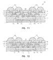
- FIG. 15illustrates a plurality of microelectronic dice 102 encapsulated with encapsulation material 112 . At least one interconnection layer is formed on the microelectronic dice active surfaces 106 and the encapsulation material first surface 110 in the manner previously discussed. The layer(s) of dielectric material and conductive traces comprising the interconnection layer is simply designated together as interconnection layer 160 in FIG. 15 .
- the individual microelectronic dice 102are then singulated along lines 162 (cut) through the interconnection layer 160 and the encapsulation material 112 to form at least one singulated microelectronic die package 150 , as shown in FIG. 11 . It is, of course, understood that the grinding process could be performed prior to singulating the individual microelectronic dice packages.
- the encapsulation material 112may include a microelectronic package core 172 surrounding the microelectronic die 102 to provide mechanical stability, as shown in FIG. 16 , to form a microelectronic die package 170 , which is similar to the microelectronic die package 150 of FIG. 11 .
- the microelectronic package core 172is position adjacent to said microelectronic die 102 , preferably substantially surrounding said microelectronic die 102 .
- the encapsulation material 112is disposed in the space between the microelectronic die 102 and the microelectronic package core 172 .
- the material used to fabricate the microelectronic package core 172may include, but is not limited to, a Bismaleimide Triazine (“BT”) resin based laminate material, an FR4 laminate material (a flame retarding glass/epoxy material), various polyimide laminate materials, ceramic material, and the like, and metallic materials (such as copper) and the like.
- BTBismaleimide Triazine
- FR4 laminate materiala flame retarding glass/epoxy material
- various polyimide laminate materialssuch as copper
- ceramic materialsuch as copper
- FIG. 17illustrates a plurality of microelectronic dice 102 encapsulated with encapsulation material 112 within the microelectronic package core 172 .
- the microelectronic package core 172includes a plurality of openings in which the microelectronic dice 102 reside.
- At least one interconnection layeris formed on the microelectronic dice active surfaces 106 , the microelectronic package core first surface 174 , and the encapsulation material first surface 110 in the manner previously discussed.
- interconnection layer 160The layer(s) of dielectric material and conductive traces comprising the interconnection layer is simply designated together as interconnection layer 160 in FIG. 17 .
- the individual microelectronic dice 102are then singulated along lines 162 (cut) through the interconnection layer 160 and the microelectronic package core 172 to form at least one singulated microelectronic die package 170 , as shown in FIG. 16 . It is, of course, understood that the grinding process could be performed prior to singulating the individual microelectronic dice packages.
Landscapes
- Engineering & Computer Science (AREA)
- Microelectronics & Electronic Packaging (AREA)
- Computer Hardware Design (AREA)
- Power Engineering (AREA)
- Physics & Mathematics (AREA)
- Condensed Matter Physics & Semiconductors (AREA)
- General Physics & Mathematics (AREA)
- Manufacturing & Machinery (AREA)
- Encapsulation Of And Coatings For Semiconductor Or Solid State Devices (AREA)
Abstract
Description
This U.S. Patent application is a continuation of U.S. patent application Ser. No. 09/691,738 filed Oct. 18, 2000, now issued as U.S. Pat. No. 6,423,570.
1. Field of the Invention
The present invention relates to apparatus and processes for packaging microelectronic dice. In particular, the present invention relates to a packaging technology that encapsulates a microelectronic die with an encapsulation material and utilizes a metallization layer to attach a heat spreader to the microelectronic die.
2. State of the Art
Higher performance, lower cost, increased miniaturization of integrated circuit components, and greater packaging density of integrated circuits are ongoing goals of the computer industry. As these goals are achieved, microelectronic dice become smaller. Of course, the goal of greater packaging density requires that the entire microelectronic die package be equal to or only slightly larger (about 10% to 30%) than the size of the microelectronic die itself. Such microelectronic die packaging is called a “chip scale packaging” or “CSP”. However in such true CSP, the surface area provided by the microelectronic die active surface generally does not provide enough surface for all of the external contacts needed to contact the external component (not shown) for certain types of microelectronic dice (i.e., logic).
Additional surface area can be provided through the use of an interposer, such as a substrate (substantially rigid material) or a flex component (substantially flexible material)FIG. 18 illustrates asubstrate interposer 222 having a microelectronic die224 attached to and in electrical contact with afirst surface 226 of the substrate interposer222 throughsmall solder balls 228. Thesmall solder balls 228 extend betweencontacts 232 on the microelectronic die224 andconductive traces 234 on the substrate interposerfirst surface 226. Theconductive traces 234 are in discrete electrical contact withbond pads 236 on asecond surface 238 of the substrate interposer222 throughvias 242 that extend through thesubstrate interposer 222. External contacts244 (shown as solder balls) are formed on thebond pads 236. Theexternal contacts 244 are utilized to achieve electrical communication between the microelectronic die224 and an external electrical system (not shown).
The use of thesubstrate interposer 222 requires number of processing steps. These processing steps increase the cost of the package. Additionally, even the use of thesmall solder balls 228 presents crowding problems which can result in shorting between thesmall solder balls 228 and can present difficulties in inserting underfilling between the microelectronic die224 and the substrate interposer222 to prevent contamination and provide mechanical stability.
Another problem arising from the fabrication of a smaller microelectronic dice is that the density of power consumption of the integrated circuit components in the microelectronic dice has increased, which, in turn, increases the average junction temperature of the dice. If the temperature of the microelectronic die becomes too high, the integrated circuits of the semiconductor die may be damaged or destroyed. Furthermore, for microelectronic dice of equivalent size, the overall power increases which presents the same problem of increased power density.
Thus, it may be necessary to attach a heat spreader to the microelectronic die.FIG. 20 illustrates aheat spreader 288 attached to themicroelectronic die 256 as shown in FIG.19. However, prior to attaching theheat spreader 288 to the microelectronic256, aback surface 286 of themicroelectronic die 256 must be exposed. This is generally achieved by grinding away the back surface284 (seeFIG. 19 ) of theencapsulation material 264 which can damage themicroelectronic die 256.
Therefore, it would be advantageous to develop new apparatus and techniques to expose the back surface of a microelectronic die for attachment of a heat spreader with potentially damaging the microelectronic die.
While the specification concludes with claims particularly pointing out and distinctly claiming that which is regarded as the present invention, the advantages of this invention can be more readily ascertained from the following description of the invention when read in conjunction with the accompanying drawings in which:
In the following detailed description, reference is made to the accompanying drawings that show, by way of illustration, specific embodiments in which the invention may be practiced. These embodiments are described in sufficient detail to enable though skilled in the art to practice the invention. It is to be understood that the various embodiments of the invention, although different, are not necessarily mutually exclusive. For example, a particular feature, structure, or characteristic described herein, in connection with one embodiment, may be implement within other embodiments without departing from the spirit and scope of the invention. In addition, it is to be understood that the location or arrangement of individual elements within each disclosed embodiment may be modified without departing from the spirit and scope of the invention. The following detailed description is, therefore, not to be taken in a limiting sense, and the scope of the present invention is defined only by the appended claims, appropriately interpreted, along with the full range of equivalents to which the claims are entitled. In the drawings, like numerals refer to the same or similar functionality throughout the several views.
The present invention relates to a packaging technology that fabricates interconnection layers on an encapsulated microelectronic die and on the encapsulation material that covers the microelectronic die. An exemplary microelectronic package includes a microelectronic die having an active surface and at least one side. An encapsulation material is disposed adjacent the microelectronic die side(s). A portion of the encapsulation material is removed to expose a back surface of the microelectronic die which has a metallization layer disposed thereon. A protective layer is disposed on the metallization layer prior to encapsulation, such that when the portion of the encapsulation material is removed, the protective layer prevents the metallization layer from being damaged. After the portion of the encapsulation material is removed, the protective layer is removed and the metallization layer is exposed. A heat spreader may then be attached to the microelectronic die by abutting the heat spreader against the metallization layer and reflowing the metallization layer.
Theprotective film 104 is preferably a substantially flexible material, such as Kapton® polyimide film (E. I. du Pont de Nemours and Company, Wilmington, Del.), but may be made of any appropriate material, including metallic films. Theprotective film 104 may have a weak adhesive, such as silicone or acrylic, which attaches to the microelectronic dieactive surface 106. This adhesive-type film may be applied prior to placing the microelectronic die102 in a mold, liquid dispense encapsulation system (preferred), or other such equipment used for the encapsulation process. Theprotective film 104 may also be a non-adhesive film, such as a ETFE (ethylene-tetrafluoroethylene) or Teflon® film, which is held on the microelectronic dieactive surface 106 by an inner surface of the mold or other such equipment during the encapsulation process.
The microelectronic die102 further includes ametallization layer 115 disposed on theback surface 114 thereof. Themetallization layer 115 is used to achieve a thermally conductive bond betweenmicroelectronic die 102 and a subsequently attached heat spreader142 (shown in FIG.1). Themetallization layer 115 is preferably formed on a semiconductor wafer (not shown) prior to dicing the semiconductor wafer into individualmicroelectronic dice 102 and preferably comprises a solder material, including, but not limited to, material such as a lead, tin, indium, gallium, bismuth, cadmium, zinc, copper, gold, silver, antimony, germanium, and alloys thereof. Themetallization layer 115 may be disposed on the semiconductor wafer (or the individual microelectronic die102) by any known technique, including but not limited to plating, sputter coating, plasma deposition, and the like. Aprotective layer 117 is disposed on themetallization layer 115. The purpose of theprotective layer 117 will be subsequently discussed. Theprotective layer 117 is preferably disposed on themetallization layer 115 prior to dicing the semiconductor wafer into individualmicroelectronic dice 102.
As shown inFIG. 3 , the microelectronic die102 is then encapsulated with anencapsulation material 112, such as plastics, resins, epoxies, elastomeric (e.g., rubbery) materials, and the like, that covers theback surface 114 and side(s)116 of themicroelectronic die 102. The encapsulation of themicroelectronic die 102 may be achieved by any known process, including but not limited to transfer and compression molding, and dispensing (preferred). Theencapsulation material 112 provides mechanical rigidity, protects the microelectronic die102 from contaminants, and provides surface area for the build-up of trace layers.
After encapsulation, theprotective film 104 is removed, as shown inFIG. 4 , to expose the microelectronic dieactive surface 106. As also shown inFIG. 4 , theencapsulation material 112 is preferably molded or dispensed to form at least one first encapsulation materialfirst surface 110 which is substantially planar to the microelectronic dieactive surface 106. The encapsulation materialfirst surface 110 will be utilized in further fabrication steps as additional surface area for the formation of interconnection layers, such as dielectric material layers and conductive traces.
Afirst dielectric layer 118, such as epoxy resin, polyimide, bisbenzocyclobutene, and the like, is disposed over the microelectronic dieactive surface 106, thecontacts 108, and the encapsulation materialfirst surface 110, as shown in FIG.5. The dielectric layers of the present invention are preferably filled epoxy resins available from Ibiden U.S.A. Corp., Santa Clara, Calif., U.S.A. and Ajinomoto U.S.A., Inc., Paramus, N.J., U.S.A. The formation of thefirst dielectric layer 118 may be achieved by any known process, including but not limited to film lamination, spin coating, roll-coating and spray-on deposition.
As shown inFIG. 6 , a plurality ofvias 122 are then formed through thefirst dielectric layer 118. The plurality ofvias 122 may be formed any method known in the art, including but not limited to laser drilling, photolithography, and, if thefirst dielectric layer 118 is photoactive, forming the plurality ofvias 122 in the same manner that a photoresist mask is made in a photolithographic process, as known in the art.
A plurality ofconductive traces 124 is formed on thefirst dielectric layer 118, as shown inFIG. 7 , wherein a portion of each of the plurality ofconductive traces 124 extends into at least one of said plurality ofvias 122 to make electrical contact with thecontacts 108. The plurality ofconductive traces 124 may be made of any applicable conductive material, such as copper, aluminum, and alloys thereof. As shown inFIG. 7 , at least one conductive trace may extend adjacent the microelectronic dieactive surface 106 and adjacent said encapsulation materialfirst surface 110.
The plurality ofconductive traces 124 may be formed by any known technique, including but not limited to semi-additive plating and photolithographic techniques. An exemplary semi-additive plating technique can involve depositing a seed layer, such as sputter-deposited or electroless-deposited metal on thefirst dielectric layer 118. A resist layer is then patterned on the seed layer, such as a titanium/copper alloy, followed by electrolytic plating of a layer of metal, such as copper, on the seed layer exposed by open areas in the patterned resist layer. The patterned resist layer is stripped and portions of the seed layer not having the layer of metal plated thereon is etched away. Other methods of forming the plurality ofconductive traces 124 will be apparent to those skilled in the art.
As shown inFIG. 8 , asecond dielectric layer 126 is disposed over the plurality ofconductive traces 124 and thefirst dielectric layer 118. The formation of thesecond dielectric layer 126 may be achieved by any known process, including but not limited to film lamination, roll-coating and spray-on deposition.
As shown inFIG. 9 a plurality ofsecond vias 128 are then formed through thesecond dielectric layer 126. The plurality ofsecond vias 128 may be formed any method known in the art, including but not limited to laser drilling and, if thesecond dielectric layer 126 is photoactive, forming the plurality ofsecond vias 128 in the same manner that a photoresist mask is made in a photolithographic process, as known in the art.
If the plurality ofconductive traces 124 is not capable of placing the plurality ofsecond vias 128 in an appropriate position, then other portions of the conductive traces are formed in the plurality ofsecond vias 128 and on thesecond dielectric layer 126, another dielectric layer formed thereon, and another plurality of vias is formed in the dielectric layer, such as described inFIGS. 7-9 . The layering of dielectric layers and the formation of conductive traces can be repeated until the vias are in an appropriate position and sufficient electrical connectivity is established to enable the required electrical performance. Thus, portions of a single conductive trace be formed from multiple portions thereof and can reside on different dielectric layers.
A second plurality ofconductive traces 132 may be formed, wherein a portion of each of the second plurality ofconductive traces 132 extends into at least one of said plurality ofsecond vias 128. The second plurality ofconductive traces 132 each include a landing pad134 (an enlarged area on the traces demarcated by a dashed line130), as shown in FIG.10.
Once the second plurality ofconductive traces 132 andlanding pads 134 are formed, they can be used in the formation of conductive interconnects, such as solder bumps, solder balls, pins, and the like, for communication with external components (not shown). For example, asolder mask material 136 can be disposed over thesecond dielectric layer 126 and the second plurality ofconductive traces 132 andlanding pads 134. A plurality of vias is then formed in thesolder mask material 136 to expose at least a portion of each of thelanding pads 134. A plurality ofconductive bumps 138, such as solder bumps, can be formed, such as by screen printing solder paste followed by a reflow process or by known plating techniques, on the exposed portion of each of thelanding pads 134, as shown inFIG. 11 , to form amicroelectronic die package 150.
Although the previous description discussed a build-up layer technique for forming theinterconnection layer 140, the present invention is not so limited. It will be understood by one skilled in the art that any known technique, including a flex component interposer, could be used to from an interconnection layer.
For the attachment of the heat spreader142 (shown in FIG.1), themetallization layer 115 must be exposed. Thus, a portion of theencapsulation material 112 must be removed to do so. This is preferably achieved by a grinding process. However, the grinding process can damage themetallization layer 115. A damagedmetallization layer 115 may result in an inefficient thermal contact between themicroelectronic die 102 and theheat spreader 142. Thus, theprotective layer 117 is utilized to prevent damage to themetallization layer 115. Theprotective layer 117 is preferably a material that is easily removed. For example, theprotective layer 117 may be a resist material, as known in the art, which can be easily, chemically dissolved. In another example, theprotective layer 117 may be a polyimide film, such as Kapton® film having a silicone or acrylic adhesive, which can be peeled cleanly off themetallization layer 115.
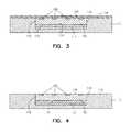
Thus, as shown inFIG. 12 , a grinding process removes a portion of theencapsulation material 112 which does not completely remove the protective layer117 (i.e., stops at or in the protective layer117). Theprotective layer 117 is then removed to expose themetallization layer 115, as shown in FIG.13.
As shown inFIG. 14 , theheat spreader 142 is then abutted against themetallization layer 115 and attached by reflowing themetallization layer 115. Anadhesive layer 144 may also be used to attach a portion of theheat spreader 142 to theencapsulation material 112. Theadhesive layer 144 is preferably pliable such that minimal thermal stress are induced on theencapsulation material 112. Theheat spreader 142 may have anelevated area 148 to compensate for the thickness of theprotective film 117. Theheat spreader 142 is preferably a highly thermally conductive material, including but not limited to, copper, aluminum, and alloys thereof.
It is, of course, understood that themicroelectronic die package 150, as shown inFIG. 11 , can be fabricated simultaneously with a number of other microelectronic die packages.FIG. 15 illustrates a plurality ofmicroelectronic dice 102 encapsulated withencapsulation material 112. At least one interconnection layer is formed on the microelectronic diceactive surfaces 106 and the encapsulation materialfirst surface 110 in the manner previously discussed. The layer(s) of dielectric material and conductive traces comprising the interconnection layer is simply designated together asinterconnection layer 160 in FIG.15. The individualmicroelectronic dice 102 are then singulated along lines162 (cut) through theinterconnection layer 160 and theencapsulation material 112 to form at least one singulatedmicroelectronic die package 150, as shown in FIG.11. It is, of course, understood that the grinding process could be performed prior to singulating the individual microelectronic dice packages.
It is further understood that theencapsulation material 112 may include amicroelectronic package core 172 surrounding the microelectronic die102 to provide mechanical stability, as shown inFIG. 16 , to form amicroelectronic die package 170, which is similar to themicroelectronic die package 150 of FIG.11. Themicroelectronic package core 172 is position adjacent to saidmicroelectronic die 102, preferably substantially surrounding saidmicroelectronic die 102. Theencapsulation material 112 is disposed in the space between themicroelectronic die 102 and themicroelectronic package core 172. The material used to fabricate themicroelectronic package core 172 may include, but is not limited to, a Bismaleimide Triazine (“BT”) resin based laminate material, an FR4 laminate material (a flame retarding glass/epoxy material), various polyimide laminate materials, ceramic material, and the like, and metallic materials (such as copper) and the like.
It is yet further understood that themicroelectronic die package 170, as shown inFIG. 16 , can also be fabricated simultaneously with a number of other microelectronic die packages.FIG. 17 illustrates a plurality ofmicroelectronic dice 102 encapsulated withencapsulation material 112 within themicroelectronic package core 172. Preferably, themicroelectronic package core 172 includes a plurality of openings in which themicroelectronic dice 102 reside. At least one interconnection layer is formed on the microelectronic diceactive surfaces 106, the microelectronic package core first surface174, and the encapsulation materialfirst surface 110 in the manner previously discussed. The layer(s) of dielectric material and conductive traces comprising the interconnection layer is simply designated together asinterconnection layer 160 in FIG.17. The individualmicroelectronic dice 102 are then singulated along lines162 (cut) through theinterconnection layer 160 and themicroelectronic package core 172 to form at least one singulatedmicroelectronic die package 170, as shown in FIG.16. It is, of course, understood that the grinding process could be performed prior to singulating the individual microelectronic dice packages.
Having thus described in detail embodiments of the present invention, it is understood that the invention defined by the appended claims is not to be limited by particular details set forth in the above description, as many apparent variations thereof are possible without departing from the spirit or scope thereof.
Claims (16)
1. A method of fabricating a microelectronic package, comprising:
providing at least one microelectronic die having an active surface, a back surface, and at least one side;
disposing a metallization layer on said microelectronic die back surface;
disposing a protection layer on said metallization layer;
abutting a protective film against said at least one microelectronic die active surface;
encapsulating said at least one microelectronic die with an encapsulation material adjacent said at least one microelectronic die side;
removing a portion of said encapsulation material to expose said protective layer; and
removing said protective layer to expose said metallization layer.
2. The method ofclaim 1 , further including attaching a heat spreader to said metallization layer by reflowing said metallization layer.
3. The method ofclaim 2 , further including disposing an adhesive material between said heat spreader and a back surface of said encapsulation material.
4. The method ofclaim 1 , further including abutting a microelectronic package core, which substantially surrounds said at least one microelectronic die, against said protective film prior to encapsulating said at least one microelectronic die, wherein a portion of said encapsulation material is disposed between said at least one microelectronic die and said microelectronic package core after said encapsulating said at least one microelectronic die.
5. The method ofclaim 1 , further including:
removing said protective film;
forming at least one dielectric material layer on at least a portion of said microelectronic die active surface and an encapsulation material surface which abutted said protective film;
forming a via through said at least one dielectric material layer to expose a portion of said microelectronic die active surface; and
forming at least one conductive trace on said at least one dielectric material layer which extends into said via to electrically contact said microelectronic die active surface, wherein said at least one conductive trace extends adjacent said microelectronic die active surface and adjacent said encapsulation material surface.
6. The method ofclaim 5 , further including forming at least one additional dielectric material layer disposed over said at least one conductive trace and said at least one dielectric material layer.
7. The method ofclaim 6 , wherein forming said at least one conductive trace on said at least one dielectric layer further includes forming at least a portion of said at least one conductive trace to extend through and reside on said at least one additional dielectric material layer.
8. A method of fabricating a microelectronic package, comprising:
providing a plurality of microelectronic dice, each having an active surface, a back surface, and at least one side;
disposing a metallization layer on said plurality of microelectronic dice back surfaces;
disposing a protection layer on said plurality of microelectronic dice metallization layers;
abutting a protective film against said plurality of microelectronic dice active surfaces;
encapsulating said at least one microelectronic dice with an encapsulation material adjacent said plurality of microelectronic dice sides;
singulating each of said plurality of microelectronic dice;
removing a portion of said encapsulation material to expose said plurality of microelectronic dice protective layers; and
removing said plurality of microelectronic dice protective layer to expose said plurality of microelectronic dice metallization layers.
9. The method ofclaim 8 , further including attaching a heat spreader to each of said microelectronic dice metallization layer by reflowing said metallization layer.
10. The method ofclaim 9 , further including disposing an adhesive material between said heat spreader and a back surface of said encapsulation material.
11. The method ofclaim 8 , further including:
providing a microelectronic package core having a plurality of openings therethrough; and
abutting a microelectronic package core against said protective film, such that said plurality of microelectronic dice reside within said plurality of openings in said microelectronic package core, prior to said encapsulating said plurality of microelectronic dice.
12. The method ofclaim 11 , wherein singulating said plurality of microelectronic die includes dicing through said microelectronic package core.
13. The method ofclaim 8 , further including, prior to singulating said plurality of microelectronic dice:
removing said protective film;
forming at least one dielectric material layer on at least a portion of each of said plurality of microelectronic dice active surfaces and an encapsulation material surface which abutted said protective film;
forming a via through said at least one dielectric material layer to expose a portion of said at least one of said plurality of microelectronic dice active surfaces; and
forming at least one conductive trace on said at least one dielectric material layer which extends into said via to electrically contact said at least one of said plurality of microelectronic dice active surfaces, wherein said at least one conductive trace extends adjacent said at least one microelectronic dice active surface and adjacent said encapsulation material surface.
14. The method ofclaim 13 , further including forming at least one additional dielectric material layer disposed over said at least one conductive trace and said at least one dielectric material layer.
15. The method ofclaim 14 , wherein forming said at least one conductive trace on said at least one dielectric layer further includes forming at least a portion of said at least one conductive trace to extend through and reside on said at least one additional dielectric material layer.
16. The method ofclaim 8 , wherein singulating said plurality of microelectronic die includes dicing through said encapsulation material.
Priority Applications (1)
| Application Number | Priority Date | Filing Date | Title |
|---|---|---|---|
| US10/137,081US6964889B2 (en) | 2000-10-18 | 2002-05-01 | Method to protect an encapsulated die package during back grinding with a solder metallization layer and devices formed thereby |
Applications Claiming Priority (2)
| Application Number | Priority Date | Filing Date | Title |
|---|---|---|---|
| US09/691,738US6423570B1 (en) | 2000-10-18 | 2000-10-18 | Method to protect an encapsulated die package during back grinding with a solder metallization layer and devices formed thereby |
| US10/137,081US6964889B2 (en) | 2000-10-18 | 2002-05-01 | Method to protect an encapsulated die package during back grinding with a solder metallization layer and devices formed thereby |
Related Parent Applications (1)
| Application Number | Title | Priority Date | Filing Date |
|---|---|---|---|
| US09/691,738ContinuationUS6423570B1 (en) | 2000-10-18 | 2000-10-18 | Method to protect an encapsulated die package during back grinding with a solder metallization layer and devices formed thereby |
Publications (2)
| Publication Number | Publication Date |
|---|---|
| US20020127780A1 US20020127780A1 (en) | 2002-09-12 |
| US6964889B2true US6964889B2 (en) | 2005-11-15 |
Family
ID=24777747
Family Applications (3)
| Application Number | Title | Priority Date | Filing Date |
|---|---|---|---|
| US09/691,738Expired - Fee RelatedUS6423570B1 (en) | 2000-10-18 | 2000-10-18 | Method to protect an encapsulated die package during back grinding with a solder metallization layer and devices formed thereby |
| US10/137,081Expired - Fee RelatedUS6964889B2 (en) | 2000-10-18 | 2002-05-01 | Method to protect an encapsulated die package during back grinding with a solder metallization layer and devices formed thereby |
| US10/143,340Expired - Fee RelatedUS6902950B2 (en) | 2000-10-18 | 2002-05-10 | Method to protect an encapsulated die package during back grinding with a solder metallization layer and devices formed thereby |
Family Applications Before (1)
| Application Number | Title | Priority Date | Filing Date |
|---|---|---|---|
| US09/691,738Expired - Fee RelatedUS6423570B1 (en) | 2000-10-18 | 2000-10-18 | Method to protect an encapsulated die package during back grinding with a solder metallization layer and devices formed thereby |
Family Applications After (1)
| Application Number | Title | Priority Date | Filing Date |
|---|---|---|---|
| US10/143,340Expired - Fee RelatedUS6902950B2 (en) | 2000-10-18 | 2002-05-10 | Method to protect an encapsulated die package during back grinding with a solder metallization layer and devices formed thereby |
Country Status (1)
| Country | Link |
|---|---|
| US (3) | US6423570B1 (en) |
Cited By (84)
| Publication number | Priority date | Publication date | Assignee | Title |
|---|---|---|---|---|
| US20060108697A1 (en)* | 2004-11-22 | 2006-05-25 | Wang James J H | Multi-chips semiconductor device assemblies and methods for fabricating the same |
| US20070059866A1 (en)* | 2003-12-03 | 2007-03-15 | Advanced Chip Engineering Technology Inc. | Fan out type wafer level package structure and method of the same |
| US20070077747A1 (en)* | 2005-09-30 | 2007-04-05 | John Heck | Microelectronic package having multiple conductive paths through an opening in a support substrate |
| US20070254475A1 (en)* | 2004-02-17 | 2007-11-01 | Sanyo Electric Co., Ltd. | Semiconductor device with a barrier layer and a metal layer |
| US20090072382A1 (en)* | 2007-09-18 | 2009-03-19 | Guzek John S | Microelectronic package and method of forming same |
| US20100006330A1 (en)* | 2008-07-11 | 2010-01-14 | Advanced Semiconductor Engineering, Inc. | Structure and process of embedded chip package |
| US20100073894A1 (en)* | 2008-09-22 | 2010-03-25 | Russell Mortensen | Coreless substrate, method of manufacturing same, and package for microelectronic device incorporating same |
| US20100078808A1 (en)* | 2008-09-29 | 2010-04-01 | Burch Kenneth R | Packaging having two devices and method of forming thereof |
| US20100081234A1 (en)* | 2008-09-29 | 2010-04-01 | Lytle William H | Method of forming a package with exposed component surfaces |
| US7851905B2 (en) | 2007-09-26 | 2010-12-14 | Intel Corporation | Microelectronic package and method of cooling an interconnect feature in same |
| US20110101491A1 (en)* | 2007-09-25 | 2011-05-05 | Oswald Skeete | Integrated circuit packages including high density bump-less build up layers and a lesser density core or coreless substrate |
| US20110108999A1 (en)* | 2009-11-06 | 2011-05-12 | Nalla Ravi K | Microelectronic package and method of manufacturing same |
| US20110156231A1 (en)* | 2009-12-29 | 2011-06-30 | Intel Corporation | Recessed and embedded die coreless package |
| US8035213B2 (en) | 2007-10-22 | 2011-10-11 | Advanced Semiconductor Engineering, Inc. | Chip package structure and method of manufacturing the same |
| US8035216B2 (en) | 2008-02-22 | 2011-10-11 | Intel Corporation | Integrated circuit package and method of manufacturing same |
| US8093704B2 (en) | 2008-06-03 | 2012-01-10 | Intel Corporation | Package on package using a bump-less build up layer (BBUL) package |
| US8304913B2 (en) | 2010-09-24 | 2012-11-06 | Intel Corporation | Methods of forming fully embedded bumpless build-up layer packages and structures formed thereby |
| US8313958B2 (en) | 2010-05-12 | 2012-11-20 | Intel Corporation | Magnetic microelectronic device attachment |
| US8320134B2 (en) | 2010-02-05 | 2012-11-27 | Advanced Semiconductor Engineering, Inc. | Embedded component substrate and manufacturing methods thereof |
| US8319318B2 (en) | 2010-04-06 | 2012-11-27 | Intel Corporation | Forming metal filled die back-side film for electromagnetic interference shielding with coreless packages |
| US8372666B2 (en) | 2010-07-06 | 2013-02-12 | Intel Corporation | Misalignment correction for embedded microelectronic die applications |
| US8434668B2 (en) | 2010-05-12 | 2013-05-07 | Intel Corporation | Magnetic attachment structure |
| US8487426B2 (en) | 2011-03-15 | 2013-07-16 | Advanced Semiconductor Engineering, Inc. | Semiconductor package with embedded die and manufacturing methods thereof |
| US8535989B2 (en) | 2010-04-02 | 2013-09-17 | Intel Corporation | Embedded semiconductive chips in reconstituted wafers, and systems containing same |
| US20130249080A1 (en)* | 2012-03-21 | 2013-09-26 | Stats Chippac, Ltd. | Semiconductor Device and Method for Forming Openings and Trenches in Insulating Layer by First LDA and Second LDA for RDL Formation |
| US20130249104A1 (en)* | 2012-03-20 | 2013-09-26 | Stats Chippac, Ltd. | Semiconductor Device and Method of Forming Conductive Layer Over Metal Substrate for Electrical Interconnect of Semiconductor Die |
| US8569894B2 (en) | 2010-01-13 | 2013-10-29 | Advanced Semiconductor Engineering, Inc. | Semiconductor package with single sided substrate design and manufacturing methods thereof |
| US8609532B2 (en) | 2010-05-26 | 2013-12-17 | Intel Corporation | Magnetically sintered conductive via |
| US8618652B2 (en) | 2010-04-16 | 2013-12-31 | Intel Corporation | Forming functionalized carrier structures with coreless packages |
| US8754516B2 (en) | 2010-08-26 | 2014-06-17 | Intel Corporation | Bumpless build-up layer package with pre-stacked microelectronic devices |
| US8848380B2 (en) | 2011-06-30 | 2014-09-30 | Intel Corporation | Bumpless build-up layer package warpage reduction |
| US8901724B2 (en) | 2009-12-29 | 2014-12-02 | Intel Corporation | Semiconductor package with embedded die and its methods of fabrication |
| US8937382B2 (en) | 2011-06-27 | 2015-01-20 | Intel Corporation | Secondary device integration into coreless microelectronic device packages |
| US8939347B2 (en) | 2010-04-28 | 2015-01-27 | Intel Corporation | Magnetic intermetallic compound interconnect |
| US9257368B2 (en) | 2012-05-14 | 2016-02-09 | Intel Corporation | Microelectric package utilizing multiple bumpless build-up structures and through-silicon vias |
| US20160126196A1 (en) | 2014-11-03 | 2016-05-05 | Rf Micro Devices, Inc. | Printed circuit module having a semiconductor device with a protective layer in place of a low-resistivity handle layer |
| US9349611B2 (en) | 2010-03-22 | 2016-05-24 | Advanced Semiconductor Engineering, Inc. | Stackable semiconductor package and manufacturing method thereof |
| US9406658B2 (en) | 2010-12-17 | 2016-08-02 | Advanced Semiconductor Engineering, Inc. | Embedded component device and manufacturing methods thereof |
| US9685390B2 (en) | 2012-06-08 | 2017-06-20 | Intel Corporation | Microelectronic package having non-coplanar, encapsulated microelectronic devices and a bumpless build-up layer |
| US9818719B2 (en) | 2010-06-30 | 2017-11-14 | Intel Corporation | Bumpless build-up layer package design with an interposer |
| US9847308B2 (en) | 2010-04-28 | 2017-12-19 | Intel Corporation | Magnetic intermetallic compound interconnect |
| US20180019184A1 (en) | 2016-07-18 | 2018-01-18 | Qorvo Us, Inc. | Thermally enhanced semiconductor package having field effect transistors with back-gate feature |
| US20180044177A1 (en)* | 2016-08-12 | 2018-02-15 | Qorvo Us, Inc. | Wafer-level package with enhanced performance |
| US10020405B2 (en) | 2016-01-19 | 2018-07-10 | Qorvo Us, Inc. | Microelectronics package with integrated sensors |
| US10020206B2 (en) | 2015-03-25 | 2018-07-10 | Qorvo Us, Inc. | Encapsulated dies with enhanced thermal performance |
| US20180197803A1 (en) | 2016-06-10 | 2018-07-12 | Qorvo Us, Inc. | Thermally enhanced semiconductor package with thermal additive and process for making the same |
| US10038055B2 (en) | 2015-05-22 | 2018-07-31 | Qorvo Us, Inc. | Substrate structure with embedded layer for post-processing silicon handle elimination |
| US20180228030A1 (en) | 2014-10-01 | 2018-08-09 | Qorvo Us, Inc. | Method for manufacturing an integrated circuit package |
| US10062637B2 (en) | 2013-10-31 | 2018-08-28 | Qorvo Us, Inc. | Method of manufacture for a semiconductor device |
| US10062583B2 (en) | 2016-05-09 | 2018-08-28 | Qorvo Us, Inc. | Microelectronics package with inductive element and magnetically enhanced mold compound component |
| US10068831B2 (en) | 2016-12-09 | 2018-09-04 | Qorvo Us, Inc. | Thermally enhanced semiconductor package and process for making the same |
| US10090339B2 (en) | 2016-10-21 | 2018-10-02 | Qorvo Us, Inc. | Radio frequency (RF) switch |
| US10109502B2 (en) | 2016-09-12 | 2018-10-23 | Qorvo Us, Inc. | Semiconductor package with reduced parasitic coupling effects and process for making the same |
| US10109550B2 (en) | 2016-08-12 | 2018-10-23 | Qorvo Us, Inc. | Wafer-level package with enhanced performance |
| US10134627B2 (en) | 2013-03-06 | 2018-11-20 | Qorvo Us, Inc. | Silicon-on-plastic semiconductor device with interfacial adhesion layer |
| US20190013255A1 (en) | 2017-07-06 | 2019-01-10 | Qorvo Us, Inc. | Wafer-level packaging for enhanced performance |
| US20190074271A1 (en) | 2017-09-05 | 2019-03-07 | Qorvo Us, Inc. | Microelectronics package with self-aligned stacked-die assembly |
| US20190074263A1 (en) | 2017-09-05 | 2019-03-07 | Qorvo Us, Inc. | Microelectronics package with self-aligned stacked-die assembly |
| TWI655739B (en)* | 2018-04-19 | 2019-04-01 | 南亞電路板股份有限公司 | Package structure and forming method thereof |
| US10276495B2 (en) | 2015-09-11 | 2019-04-30 | Qorvo Us, Inc. | Backside semiconductor die trimming |
| US10486963B2 (en) | 2016-08-12 | 2019-11-26 | Qorvo Us, Inc. | Wafer-level package with enhanced performance |
| US20200235054A1 (en) | 2019-01-23 | 2020-07-23 | Qorvo Us, Inc. | Rf devices with enhanced performance and methods of forming the same |
| US10749518B2 (en) | 2016-11-18 | 2020-08-18 | Qorvo Us, Inc. | Stacked field-effect transistor switch |
| US10773952B2 (en) | 2016-05-20 | 2020-09-15 | Qorvo Us, Inc. | Wafer-level package with enhanced performance |
| US10784149B2 (en) | 2016-05-20 | 2020-09-22 | Qorvo Us, Inc. | Air-cavity module with enhanced device isolation |
| US10804246B2 (en) | 2018-06-11 | 2020-10-13 | Qorvo Us, Inc. | Microelectronics package with vertically stacked dies |
| US10964554B2 (en) | 2018-10-10 | 2021-03-30 | Qorvo Us, Inc. | Wafer-level fan-out package with enhanced performance |
| US11069590B2 (en) | 2018-10-10 | 2021-07-20 | Qorvo Us, Inc. | Wafer-level fan-out package with enhanced performance |
| US20210296199A1 (en) | 2018-11-29 | 2021-09-23 | Qorvo Us, Inc. | Thermally enhanced semiconductor package with at least one heat extractor and process for making the same |
| US11152363B2 (en) | 2018-03-28 | 2021-10-19 | Qorvo Us, Inc. | Bulk CMOS devices with enhanced performance and methods of forming the same utilizing bulk CMOS process |
| US20220108938A1 (en) | 2019-01-23 | 2022-04-07 | Qorvo Us, Inc. | Rf devices with enhanced performance and methods of forming the same |
| US20220139862A1 (en) | 2019-01-23 | 2022-05-05 | Qorvo Us, Inc. | Rf devices with enhanced performance and methods of forming the same |
| US11387157B2 (en) | 2019-01-23 | 2022-07-12 | Qorvo Us, Inc. | RF devices with enhanced performance and methods of forming the same |
| US11646289B2 (en) | 2019-12-02 | 2023-05-09 | Qorvo Us, Inc. | RF devices with enhanced performance and methods of forming the same |
| US11923238B2 (en) | 2019-12-12 | 2024-03-05 | Qorvo Us, Inc. | Method of forming RF devices with enhanced performance including attaching a wafer to a support carrier by a bonding technique without any polymer adhesive |
| US12046535B2 (en) | 2018-07-02 | 2024-07-23 | Qorvo Us, Inc. | RF devices with enhanced performance and methods of forming the same |
| US12046483B2 (en) | 2019-01-23 | 2024-07-23 | Qorvo Us, Inc. | RF devices with enhanced performance and methods of forming the same |
| US12046505B2 (en) | 2018-04-20 | 2024-07-23 | Qorvo Us, Inc. | RF devices with enhanced performance and methods of forming the same utilizing localized SOI formation |
| US12062701B2 (en) | 2018-04-04 | 2024-08-13 | Qorvo Us, Inc. | Gallium-nitride-based module with enhanced electrical performance and process for making the same |
| US12062571B2 (en) | 2021-03-05 | 2024-08-13 | Qorvo Us, Inc. | Selective etching process for SiGe and doped epitaxial silicon |
| US12074086B2 (en) | 2019-11-01 | 2024-08-27 | Qorvo Us, Inc. | RF devices with nanotube particles for enhanced performance and methods of forming the same |
| US12125825B2 (en) | 2019-01-23 | 2024-10-22 | Qorvo Us, Inc. | RF devices with enhanced performance and methods of forming the same |
| US12129168B2 (en) | 2019-12-23 | 2024-10-29 | Qorvo Us, Inc. | Microelectronics package with vertically stacked MEMS device and controller device |
| US12266587B2 (en) | 2022-06-08 | 2025-04-01 | STATS ChipPAC Pte. Ltd. | Semiconductor device and method for advanced thermal dissipation |
Families Citing this family (174)
| Publication number | Priority date | Publication date | Assignee | Title |
|---|---|---|---|---|
| US6287890B1 (en)* | 1999-10-18 | 2001-09-11 | Thin Film Module, Inc. | Low cost decal material used for packaging |
| JP3998878B2 (en)* | 1999-11-25 | 2007-10-31 | シャープ株式会社 | Semiconductor device, semiconductor device manufacturing method, and package manufacturing method |
| JP4403631B2 (en)* | 2000-04-24 | 2010-01-27 | ソニー株式会社 | Manufacturing method of chip-shaped electronic component and manufacturing method of pseudo wafer used for manufacturing the same |
| US20020020898A1 (en)* | 2000-08-16 | 2002-02-21 | Vu Quat T. | Microelectronic substrates with integrated devices |
| US6709898B1 (en)* | 2000-10-04 | 2004-03-23 | Intel Corporation | Die-in-heat spreader microelectronic package |
| US6423570B1 (en)* | 2000-10-18 | 2002-07-23 | Intel Corporation | Method to protect an encapsulated die package during back grinding with a solder metallization layer and devices formed thereby |
| US6890829B2 (en)* | 2000-10-24 | 2005-05-10 | Intel Corporation | Fabrication of on-package and on-chip structure using build-up layer process |
| US20020070443A1 (en)* | 2000-12-08 | 2002-06-13 | Xiao-Chun Mu | Microelectronic package having an integrated heat sink and build-up layers |
| US6555906B2 (en)* | 2000-12-15 | 2003-04-29 | Intel Corporation | Microelectronic package having a bumpless laminated interconnection layer |
| US6706553B2 (en)* | 2001-03-26 | 2004-03-16 | Intel Corporation | Dispensing process for fabrication of microelectronic packages |
| US7498196B2 (en)* | 2001-03-30 | 2009-03-03 | Megica Corporation | Structure and manufacturing method of chip scale package |
| US7115986B2 (en) | 2001-05-02 | 2006-10-03 | Micron Technology, Inc. | Flexible ball grid array chip scale packages |
| US20030059976A1 (en)* | 2001-09-24 | 2003-03-27 | Nathan Richard J. | Integrated package and methods for making same |
| US6673698B1 (en) | 2002-01-19 | 2004-01-06 | Megic Corporation | Thin film semiconductor package utilizing a glass substrate with composite polymer/metal interconnect layers |
| TW517361B (en) | 2001-12-31 | 2003-01-11 | Megic Corp | Chip package structure and its manufacture process |
| TW503496B (en) | 2001-12-31 | 2002-09-21 | Megic Corp | Chip packaging structure and manufacturing process of the same |
| TW584950B (en) | 2001-12-31 | 2004-04-21 | Megic Corp | Chip packaging structure and process thereof |
| TW544882B (en) | 2001-12-31 | 2003-08-01 | Megic Corp | Chip package structure and process thereof |
| US6841413B2 (en)* | 2002-01-07 | 2005-01-11 | Intel Corporation | Thinned die integrated circuit package |
| US20050136640A1 (en)* | 2002-01-07 | 2005-06-23 | Chuan Hu | Die exhibiting an effective coefficient of thermal expansion equivalent to a substrate mounted thereon, and processes of making same |
| SG104293A1 (en) | 2002-01-09 | 2004-06-21 | Micron Technology Inc | Elimination of rdl using tape base flip chip on flex for die stacking |
| US6988531B2 (en)* | 2002-01-11 | 2006-01-24 | Intel Corporation | Micro-chimney and thermosiphon die-level cooling |
| SG115455A1 (en) | 2002-03-04 | 2005-10-28 | Micron Technology Inc | Methods for assembly and packaging of flip chip configured dice with interposer |
| SG121707A1 (en) | 2002-03-04 | 2006-05-26 | Micron Technology Inc | Method and apparatus for flip-chip packaging providing testing capability |
| SG115459A1 (en)* | 2002-03-04 | 2005-10-28 | Micron Technology Inc | Flip chip packaging using recessed interposer terminals |
| SG115456A1 (en) | 2002-03-04 | 2005-10-28 | Micron Technology Inc | Semiconductor die packages with recessed interconnecting structures and methods for assembling the same |
| US6975035B2 (en)* | 2002-03-04 | 2005-12-13 | Micron Technology, Inc. | Method and apparatus for dielectric filling of flip chip on interposer assembly |
| SG111935A1 (en) | 2002-03-04 | 2005-06-29 | Micron Technology Inc | Interposer configured to reduce the profiles of semiconductor device assemblies and packages including the same and methods |
| WO2004015771A2 (en)* | 2002-08-09 | 2004-02-19 | Casio Computer Co., Ltd. | Semiconductor device and method of manufacturing the same |
| US20040036170A1 (en) | 2002-08-20 | 2004-02-26 | Lee Teck Kheng | Double bumping of flexible substrate for first and second level interconnects |
| DE10238816B4 (en)* | 2002-08-23 | 2008-01-10 | Qimonda Ag | Method of making connection areas of an integrated circuit and integrated circuit with connection areas |
| US6964881B2 (en) | 2002-08-27 | 2005-11-15 | Micron Technology, Inc. | Multi-chip wafer level system packages and methods of forming same |
| JP3617647B2 (en)* | 2002-11-08 | 2005-02-09 | 沖電気工業株式会社 | Semiconductor device and manufacturing method thereof |
| US7135780B2 (en) | 2003-02-12 | 2006-11-14 | Micron Technology, Inc. | Semiconductor substrate for build-up packages |
| JP3813945B2 (en)* | 2003-05-07 | 2006-08-23 | 任天堂株式会社 | GAME DEVICE AND GAME PROGRAM |
| JP2004349361A (en)* | 2003-05-21 | 2004-12-09 | Casio Comput Co Ltd | Semiconductor device and method of manufacturing the same |
| TWI286372B (en)* | 2003-08-13 | 2007-09-01 | Phoenix Prec Technology Corp | Semiconductor package substrate with protective metal layer on pads formed thereon and method for fabricating the same |
| US7132746B2 (en)* | 2003-08-18 | 2006-11-07 | Delphi Technologies, Inc. | Electronic assembly with solder-bonded heat sink |
| US7514767B2 (en)* | 2003-12-03 | 2009-04-07 | Advanced Chip Engineering Technology Inc. | Fan out type wafer level package structure and method of the same |
| TWI245350B (en)* | 2004-03-25 | 2005-12-11 | Siliconware Precision Industries Co Ltd | Wafer level semiconductor package with build-up layer |
| TWI237883B (en)* | 2004-05-11 | 2005-08-11 | Via Tech Inc | Chip embedded package structure and process thereof |
| JP4528062B2 (en)* | 2004-08-25 | 2010-08-18 | 富士通株式会社 | Semiconductor device and manufacturing method thereof |
| JP2006100666A (en)* | 2004-09-30 | 2006-04-13 | Toshiba Corp | Semiconductor device and manufacturing method thereof |
| KR101313391B1 (en) | 2004-11-03 | 2013-10-01 | 테세라, 인코포레이티드 | Stacked packaging improvements |
| TWI246759B (en)* | 2004-11-16 | 2006-01-01 | Siliconware Precision Industries Co Ltd | Heat dissipating package structure and fabrication method thereof |
| TWI301660B (en)* | 2004-11-26 | 2008-10-01 | Phoenix Prec Technology Corp | Structure of embedding chip in substrate and method for fabricating the same |
| CN100388447C (en)* | 2004-12-20 | 2008-05-14 | 全懋精密科技股份有限公司 | Chip embedded substrate structure of semiconductor package and manufacturing method thereof |
| JP4790297B2 (en)* | 2005-04-06 | 2011-10-12 | ルネサスエレクトロニクス株式会社 | Semiconductor device and manufacturing method thereof |
| US20070000595A1 (en)* | 2005-06-29 | 2007-01-04 | Intel Corporation | Adhesive substrate and method for using |
| CN100559561C (en)* | 2005-08-17 | 2009-11-11 | 南茂科技股份有限公司 | Cavity-down chip package and method for manufacturing the same |
| TWI279897B (en)* | 2005-12-23 | 2007-04-21 | Phoenix Prec Technology Corp | Embedded semiconductor chip structure and method for fabricating the same |
| US8058101B2 (en) | 2005-12-23 | 2011-11-15 | Tessera, Inc. | Microelectronic packages and methods therefor |
| US7342303B1 (en)* | 2006-02-28 | 2008-03-11 | Amkor Technology, Inc. | Semiconductor device having RF shielding and method therefor |
| US20070212813A1 (en)* | 2006-03-10 | 2007-09-13 | Fay Owen R | Perforated embedded plane package and method |
| DE102006030267B4 (en)* | 2006-06-30 | 2009-04-16 | Advanced Micro Devices, Inc., Sunnyvale | Nano embossing technique with increased flexibility in terms of adjustment and shaping of structural elements |
| US7569422B2 (en)* | 2006-08-11 | 2009-08-04 | Megica Corporation | Chip package and method for fabricating the same |
| TWI325745B (en) | 2006-11-13 | 2010-06-01 | Unimicron Technology Corp | Circuit board structure and fabrication method thereof |
| AU2008232360A1 (en) | 2007-03-23 | 2008-10-02 | Allegiance Corporation | Fluid collection and disposal system having internchangeable collection and other features and methods relating thereof |
| US9889239B2 (en) | 2007-03-23 | 2018-02-13 | Allegiance Corporation | Fluid collection and disposal system and related methods |
| US7926173B2 (en)* | 2007-07-05 | 2011-04-19 | Occam Portfolio Llc | Method of making a circuit assembly |
| US20080290482A1 (en)* | 2007-05-25 | 2008-11-27 | National Semiconductor Corporation | Method of packaging integrated circuits |
| US7898066B1 (en) | 2007-05-25 | 2011-03-01 | Amkor Technology, Inc. | Semiconductor device having EMI shielding and method therefor |
| US8237259B2 (en)* | 2007-06-13 | 2012-08-07 | Infineon Technologies Ag | Embedded chip package |
| KR101452548B1 (en)* | 2007-06-20 | 2014-10-21 | 스카이워크스 솔루션즈, 인코포레이티드 | Semiconductor die with backside passive device integration |
| US7745910B1 (en) | 2007-07-10 | 2010-06-29 | Amkor Technology, Inc. | Semiconductor device having RF shielding and method therefor |
| US20090170241A1 (en)* | 2007-12-26 | 2009-07-02 | Stats Chippac, Ltd. | Semiconductor Device and Method of Forming the Device Using Sacrificial Carrier |
| US20090166844A1 (en)* | 2007-12-26 | 2009-07-02 | Xuejiao Hu | Metal cover on flip-chip matrix-array (fcmx) substrate for low cost cpu assembly |
| US8008753B1 (en) | 2008-04-22 | 2011-08-30 | Amkor Technology, Inc. | System and method to reduce shorting of radio frequency (RF) shielding |
| TWI413223B (en)* | 2008-09-02 | 2013-10-21 | Unimicron Technology Corp | Package substrate having semiconductor component embedded therein and fabrication method thereof |
| US7915715B2 (en)* | 2008-11-25 | 2011-03-29 | Amkor Technology, Inc. | System and method to provide RF shielding for a MEMS microphone package |
| US8129824B1 (en) | 2008-12-03 | 2012-03-06 | Amkor Technology, Inc. | Shielding for a semiconductor package |
| US8102032B1 (en) | 2008-12-09 | 2012-01-24 | Amkor Technology, Inc. | System and method for compartmental shielding of stacked packages |
| US9082806B2 (en) | 2008-12-12 | 2015-07-14 | Stats Chippac, Ltd. | Semiconductor device and method of forming a vertical interconnect structure for 3-D FO-WLCSP |
| US9064936B2 (en) | 2008-12-12 | 2015-06-23 | Stats Chippac, Ltd. | Semiconductor device and method of forming a vertical interconnect structure for 3-D FO-WLCSP |
| US9293401B2 (en)* | 2008-12-12 | 2016-03-22 | Stats Chippac, Ltd. | Semiconductor device and method for forming a low profile embedded wafer level ball grid array molded laser package (EWLP-MLP) |
| US7642128B1 (en) | 2008-12-12 | 2010-01-05 | Stats Chippac, Ltd. | Semiconductor device and method of forming a vertical interconnect structure for 3-D FO-WLCSP |
| US8012868B1 (en) | 2008-12-15 | 2011-09-06 | Amkor Technology Inc | Semiconductor device having EMI shielding and method therefor |
| US7851894B1 (en) | 2008-12-23 | 2010-12-14 | Amkor Technology, Inc. | System and method for shielding of package on package (PoP) assemblies |
| US20100167471A1 (en) | 2008-12-30 | 2010-07-01 | Stmicroelectronics Asia Pacific Pte. Ltd. | Reducing warpage for fan-out wafer level packaging |
| US7960818B1 (en) | 2009-03-04 | 2011-06-14 | Amkor Technology, Inc. | Conformal shield on punch QFN semiconductor package |
| US8093691B1 (en) | 2009-07-14 | 2012-01-10 | Amkor Technology, Inc. | System and method for RF shielding of a semiconductor package |
| WO2011008961A1 (en) | 2009-07-15 | 2011-01-20 | Allegiance Corporation | Fluid collection and disposal system and related methods |
| US8367470B2 (en)* | 2009-08-07 | 2013-02-05 | Stats Chippac, Ltd. | Semiconductor device and method of forming cavity in build-up interconnect structure for short signal path between die |
| TWI528514B (en)* | 2009-08-20 | 2016-04-01 | 精材科技股份有限公司 | Chip package and fabrication method thereof |
| US8362598B2 (en) | 2009-08-26 | 2013-01-29 | Amkor Technology Inc | Semiconductor device with electromagnetic interference shielding |
| JP5588137B2 (en)* | 2009-09-14 | 2014-09-10 | 新光電気工業株式会社 | Manufacturing method of semiconductor device |
| US20110156239A1 (en)* | 2009-12-29 | 2011-06-30 | Stmicroelectronics Asia Pacific Pte Ltd. | Method for manufacturing a fan-out embedded panel level package |
| US8497587B2 (en)* | 2009-12-30 | 2013-07-30 | Stmicroelectronics Pte Ltd. | Thermally enhanced expanded wafer level package ball grid array structure and method of making the same |
| TWI401753B (en)* | 2009-12-31 | 2013-07-11 | Advanced Semiconductor Eng | Method for making a stackable package |
| US8199518B1 (en) | 2010-02-18 | 2012-06-12 | Amkor Technology, Inc. | Top feature package and method |
| US8946886B1 (en) | 2010-05-13 | 2015-02-03 | Amkor Technology, Inc. | Shielded electronic component package and method |
| US8508023B1 (en) | 2010-06-17 | 2013-08-13 | Amkor Technology, Inc. | System and method for lowering contact resistance of the radio frequency (RF) shield to ground |
| US8482111B2 (en) | 2010-07-19 | 2013-07-09 | Tessera, Inc. | Stackable molded microelectronic packages |
| US9159708B2 (en) | 2010-07-19 | 2015-10-13 | Tessera, Inc. | Stackable molded microelectronic packages with area array unit connectors |
| US8847376B2 (en) | 2010-07-23 | 2014-09-30 | Tessera, Inc. | Microelectronic elements with post-assembly planarization |
| TWI555100B (en)* | 2010-07-26 | 2016-10-21 | 矽品精密工業股份有限公司 | Chip scale package and fabrication method thereof |
| CN102376592B (en)* | 2010-08-10 | 2014-05-07 | 矽品精密工业股份有限公司 | Chip size package and method for making the same |
| US8502372B2 (en)* | 2010-08-26 | 2013-08-06 | Lsi Corporation | Low-cost 3D face-to-face out assembly |
| US8502367B2 (en) | 2010-09-29 | 2013-08-06 | Stmicroelectronics Pte Ltd. | Wafer-level packaging method using composite material as a base |
| KR101075241B1 (en) | 2010-11-15 | 2011-11-01 | 테세라, 인코포레이티드 | Microelectronic package with terminals in dielectric member |
| US20120146206A1 (en) | 2010-12-13 | 2012-06-14 | Tessera Research Llc | Pin attachment |
| JP2012134270A (en)* | 2010-12-21 | 2012-07-12 | Shinko Electric Ind Co Ltd | Semiconductor device and manufacturing method of the same |
| TWI426584B (en)* | 2010-12-22 | 2014-02-11 | 矽品精密工業股份有限公司 | Semiconductor package and method of forming same |
| US8823133B2 (en) | 2011-03-29 | 2014-09-02 | Xilinx, Inc. | Interposer having an inductor |
| US8618659B2 (en) | 2011-05-03 | 2013-12-31 | Tessera, Inc. | Package-on-package assembly with wire bonds to encapsulation surface |
| KR101128063B1 (en) | 2011-05-03 | 2012-04-23 | 테세라, 인코포레이티드 | Package-on-package assembly with wire bonds to encapsulation surface |
| US9679863B2 (en)* | 2011-09-23 | 2017-06-13 | STATS ChipPAC Pte. Ltd. | Semiconductor device and method of forming interconnect substrate for FO-WLCSP |
| US8836136B2 (en) | 2011-10-17 | 2014-09-16 | Invensas Corporation | Package-on-package assembly with wire bond vias |
| US8946757B2 (en) | 2012-02-17 | 2015-02-03 | Invensas Corporation | Heat spreading substrate with embedded interconnects |
| US9349706B2 (en) | 2012-02-24 | 2016-05-24 | Invensas Corporation | Method for package-on-package assembly with wire bonds to encapsulation surface |
| US8372741B1 (en) | 2012-02-24 | 2013-02-12 | Invensas Corporation | Method for package-on-package assembly with wire bonds to encapsulation surface |
| US10136516B2 (en) | 2012-03-13 | 2018-11-20 | Intel Corporation | Microelectronic device attachment on a reverse microelectronic package |
| DE112012006033B4 (en) | 2012-03-13 | 2024-09-12 | Intel Corp. | Mounting a microelectronic device on an inverted microelectronic package |
| WO2013162519A1 (en) | 2012-04-24 | 2013-10-31 | Intel Corporation | Suspended inductor microelectronic structures |
| US8835228B2 (en)* | 2012-05-22 | 2014-09-16 | Invensas Corporation | Substrate-less stackable package with wire-bond interconnect |
| TWI473217B (en)* | 2012-07-19 | 2015-02-11 | 矽品精密工業股份有限公司 | Semiconductor package and method of forming the same |
| US9391008B2 (en) | 2012-07-31 | 2016-07-12 | Invensas Corporation | Reconstituted wafer-level package DRAM |
| US9502390B2 (en) | 2012-08-03 | 2016-11-22 | Invensas Corporation | BVA interposer |
| US10622310B2 (en) | 2012-09-26 | 2020-04-14 | Ping-Jung Yang | Method for fabricating glass substrate package |
| US8975738B2 (en) | 2012-11-12 | 2015-03-10 | Invensas Corporation | Structure for microelectronic packaging with terminals on dielectric mass |
| US8878353B2 (en) | 2012-12-20 | 2014-11-04 | Invensas Corporation | Structure for microelectronic packaging with bond elements to encapsulation surface |
| US9136254B2 (en) | 2013-02-01 | 2015-09-15 | Invensas Corporation | Microelectronic package having wire bond vias and stiffening layer |
| US9167710B2 (en) | 2013-08-07 | 2015-10-20 | Invensas Corporation | Embedded packaging with preformed vias |
| US9685365B2 (en) | 2013-08-08 | 2017-06-20 | Invensas Corporation | Method of forming a wire bond having a free end |
| US20150076714A1 (en) | 2013-09-16 | 2015-03-19 | Invensas Corporation | Microelectronic element with bond elements to encapsulation surface |
| CN103474361B (en)* | 2013-09-29 | 2016-06-01 | 华进半导体封装先导技术研发中心有限公司 | A kind of embedded active packaging process and encapsulation structure imbedding function substrate |
| US9583456B2 (en) | 2013-11-22 | 2017-02-28 | Invensas Corporation | Multiple bond via arrays of different wire heights on a same substrate |
| US9263394B2 (en) | 2013-11-22 | 2016-02-16 | Invensas Corporation | Multiple bond via arrays of different wire heights on a same substrate |
| US9379074B2 (en) | 2013-11-22 | 2016-06-28 | Invensas Corporation | Die stacks with one or more bond via arrays of wire bond wires and with one or more arrays of bump interconnects |
| US9824989B2 (en)* | 2014-01-17 | 2017-11-21 | Taiwan Semiconductor Manufacturing Company, Ltd. | Fan-out package and methods of forming thereof |
| US9583411B2 (en) | 2014-01-17 | 2017-02-28 | Invensas Corporation | Fine pitch BVA using reconstituted wafer with area array accessible for testing |
| US9673171B1 (en)* | 2014-03-26 | 2017-06-06 | STATS ChipPAC Pte. Ltd. | Integrated circuit packaging system with coreless substrate and method of manufacture thereof |
| KR102250997B1 (en) | 2014-05-02 | 2021-05-12 | 삼성전자주식회사 | Semiconductor package |
| US10381326B2 (en) | 2014-05-28 | 2019-08-13 | Invensas Corporation | Structure and method for integrated circuits packaging with increased density |
| US9646917B2 (en) | 2014-05-29 | 2017-05-09 | Invensas Corporation | Low CTE component with wire bond interconnects |
| US9412714B2 (en) | 2014-05-30 | 2016-08-09 | Invensas Corporation | Wire bond support structure and microelectronic package including wire bonds therefrom |
| US9640419B2 (en) | 2014-08-04 | 2017-05-02 | Infineon Technologies Ag | Carrier system for processing semiconductor substrates, and methods thereof |
| US9368436B2 (en)* | 2014-08-04 | 2016-06-14 | Infineon Technologies Ag | Source down semiconductor devices and methods of formation thereof |
| US9721799B2 (en) | 2014-11-07 | 2017-08-01 | Advanced Semiconductor Engineering, Inc. | Semiconductor package with reduced via hole width and reduced pad patch and manufacturing method thereof |
| US10079156B2 (en) | 2014-11-07 | 2018-09-18 | Advanced Semiconductor Engineering, Inc. | Semiconductor package including dielectric layers defining via holes extending to component pads |
| US9420695B2 (en) | 2014-11-19 | 2016-08-16 | Advanced Semiconductor Engineering, Inc. | Semiconductor package structure and semiconductor process |
| US9426891B2 (en) | 2014-11-21 | 2016-08-23 | Advanced Semiconductor Engineering, Inc. | Circuit board with embedded passive component and manufacturing method thereof |
| US9735084B2 (en) | 2014-12-11 | 2017-08-15 | Invensas Corporation | Bond via array for thermal conductivity |
| US9443921B2 (en) | 2015-02-10 | 2016-09-13 | Advanced Semiconductor Engineering, Inc. | Semiconductor package structure and semiconductor manufacturing process |
| US9888579B2 (en) | 2015-03-05 | 2018-02-06 | Invensas Corporation | Pressing of wire bond wire tips to provide bent-over tips |
| US9502372B1 (en) | 2015-04-30 | 2016-11-22 | Invensas Corporation | Wafer-level packaging using wire bond wires in place of a redistribution layer |
| US9761554B2 (en) | 2015-05-07 | 2017-09-12 | Invensas Corporation | Ball bonding metal wire bond wires to metal pads |
| JP6761472B2 (en)* | 2015-08-07 | 2020-09-23 | コーボ ユーエス,インコーポレイティド | Flip chip module with enhanced properties |
| US10490528B2 (en) | 2015-10-12 | 2019-11-26 | Invensas Corporation | Embedded wire bond wires |
| US9490222B1 (en) | 2015-10-12 | 2016-11-08 | Invensas Corporation | Wire bond wires for interference shielding |
| US10332854B2 (en) | 2015-10-23 | 2019-06-25 | Invensas Corporation | Anchoring structure of fine pitch bva |
| US10181457B2 (en) | 2015-10-26 | 2019-01-15 | Invensas Corporation | Microelectronic package for wafer-level chip scale packaging with fan-out |
| US9711458B2 (en)* | 2015-11-13 | 2017-07-18 | Taiwan Semiconductor Manufacturing Company, Ltd. | Structure and formation method for chip package |
| US10043779B2 (en) | 2015-11-17 | 2018-08-07 | Invensas Corporation | Packaged microelectronic device for a package-on-package device |
| US9659848B1 (en) | 2015-11-18 | 2017-05-23 | Invensas Corporation | Stiffened wires for offset BVA |
| US9984992B2 (en) | 2015-12-30 | 2018-05-29 | Invensas Corporation | Embedded wire bond wires for vertical integration with separate surface mount and wire bond mounting surfaces |
| DE102016203453A1 (en)* | 2016-03-02 | 2017-09-07 | Fraunhofer-Gesellschaft zur Förderung der angewandten Forschung e.V. | Method for producing a semiconductor component and semiconductor component |
| US20170287838A1 (en) | 2016-04-02 | 2017-10-05 | Intel Corporation | Electrical interconnect bridge |
| US10186499B2 (en)* | 2016-06-30 | 2019-01-22 | Intel IP Corporation | Integrated circuit package assemblies including a chip recess |
| US9935075B2 (en) | 2016-07-29 | 2018-04-03 | Invensas Corporation | Wire bonding method and apparatus for electromagnetic interference shielding |
| US10299368B2 (en) | 2016-12-21 | 2019-05-21 | Invensas Corporation | Surface integrated waveguides and circuit structures therefor |
| US10177095B2 (en) | 2017-03-24 | 2019-01-08 | Amkor Technology, Inc. | Semiconductor device and method of manufacturing thereof |
| WO2018181236A1 (en)* | 2017-03-31 | 2018-10-04 | パナソニックIpマネジメント株式会社 | Semiconductor device, and method for manufacturing same |
| US10177011B2 (en)* | 2017-04-13 | 2019-01-08 | Powertech Technology Inc. | Chip packaging method by using a temporary carrier for flattening a multi-layer structure |
| US10497650B2 (en) | 2017-04-13 | 2019-12-03 | Amkor Technology, Inc. | Semiconductor device and manufacturing method thereof |
| FR3085575B1 (en) | 2018-09-03 | 2021-06-18 | St Microelectronics Tours Sas | ELECTRONIC CHIP BOX |
| US20200312732A1 (en) | 2018-09-14 | 2020-10-01 | Mediatek Inc. | Chip scale package structure and method of forming the same |
| US11450606B2 (en)* | 2018-09-14 | 2022-09-20 | Mediatek Inc. | Chip scale package structure and method of forming the same |
| KR102595864B1 (en)* | 2018-12-07 | 2023-10-30 | 삼성전자주식회사 | Semiconductor package |
| FR3093230B1 (en)* | 2019-02-27 | 2023-01-06 | St Microelectronics Tours Sas | Electronic chip box |
| US20210287953A1 (en)* | 2020-03-12 | 2021-09-16 | Didrew Technology (Bvi) Limited | Embedded molding fan-out (emfo) packaging and method of manufacturing thereof |
| US11744413B2 (en) | 2021-10-07 | 2023-09-05 | Deb Ip Limited | Dispenser assembly |
| US11887928B2 (en)* | 2021-12-17 | 2024-01-30 | Advanced Semiconductor Engineering, Inc. | Package structure with interposer encapsulated by an encapsulant |
| DE102022133833A1 (en)* | 2022-12-19 | 2024-06-20 | Infineon Technologies Ag | METHOD FOR EMBEDDING A NAKED CHIP IN A CARRIER LAMINATE |
Citations (18)
| Publication number | Priority date | Publication date | Assignee | Title |
|---|---|---|---|---|
| US5353498A (en) | 1993-02-08 | 1994-10-11 | General Electric Company | Method for fabricating an integrated circuit module |
| US5422513A (en) | 1992-10-16 | 1995-06-06 | Martin Marietta Corporation | Integrated circuit chip placement in a high density interconnect structure |
| US5455457A (en) | 1990-11-27 | 1995-10-03 | Nec Corporation | Package for semiconductor elements having thermal dissipation means |
| US5514906A (en) | 1993-11-10 | 1996-05-07 | Fujitsu Limited | Apparatus for cooling semiconductor chips in multichip modules |
| US5527741A (en) | 1994-10-11 | 1996-06-18 | Martin Marietta Corporation | Fabrication and structures of circuit modules with flexible interconnect layers |
| US5703400A (en) | 1995-12-04 | 1997-12-30 | General Electric Company | Fabrication and structures of two-sided molded circuit modules with flexible interconnect layers |
| US5745984A (en) | 1995-07-10 | 1998-05-05 | Martin Marietta Corporation | Method for making an electronic module |
| US5801070A (en)* | 1994-06-09 | 1998-09-01 | Ford Global Technologies, Inc. | High sensitivity, silicon-based, Microcalorimetric gas sensor and fabrication method |
| JPH1145955A (en) | 1997-07-28 | 1999-02-16 | Kyocera Corp | Element built-in multilayer wiring board and method of manufacturing the same |
| US5895229A (en) | 1997-05-19 | 1999-04-20 | Motorola, Inc. | Microelectronic package including a polymer encapsulated die, and method for forming same |
| JPH11312868A (en) | 1998-04-28 | 1999-11-09 | Kyocera Corp | Element built-in multilayer wiring board and method of manufacturing the same |
| US6060778A (en) | 1997-05-17 | 2000-05-09 | Hyundai Electronics Industries Co. Ltd. | Ball grid array package |
| US6154366A (en)* | 1999-11-23 | 2000-11-28 | Intel Corporation | Structures and processes for fabricating moisture resistant chip-on-flex packages |
| US6184570B1 (en) | 1999-10-28 | 2001-02-06 | Ericsson Inc. | Integrated circuit dies including thermal stress reducing grooves and microelectronic packages utilizing the same |
| US6271469B1 (en) | 1999-11-12 | 2001-08-07 | Intel Corporation | Direct build-up layer on an encapsulated die package |
| US6423570B1 (en)* | 2000-10-18 | 2002-07-23 | Intel Corporation | Method to protect an encapsulated die package during back grinding with a solder metallization layer and devices formed thereby |
| US6515356B1 (en) | 1999-05-07 | 2003-02-04 | Amkor Technology, Inc. | Semiconductor package and method for fabricating the same |
| US6586822B1 (en)* | 2000-09-08 | 2003-07-01 | Intel Corporation | Integrated core microelectronic package |
- 2000
- 2000-10-18USUS09/691,738patent/US6423570B1/ennot_activeExpired - Fee Related
- 2002
- 2002-05-01USUS10/137,081patent/US6964889B2/ennot_activeExpired - Fee Related
- 2002-05-10USUS10/143,340patent/US6902950B2/ennot_activeExpired - Fee Related
Patent Citations (19)
| Publication number | Priority date | Publication date | Assignee | Title |
|---|---|---|---|---|
| US5455457A (en) | 1990-11-27 | 1995-10-03 | Nec Corporation | Package for semiconductor elements having thermal dissipation means |
| US5422513A (en) | 1992-10-16 | 1995-06-06 | Martin Marietta Corporation | Integrated circuit chip placement in a high density interconnect structure |
| US5353498A (en) | 1993-02-08 | 1994-10-11 | General Electric Company | Method for fabricating an integrated circuit module |
| US5497033A (en)* | 1993-02-08 | 1996-03-05 | Martin Marietta Corporation | Embedded substrate for integrated circuit modules |
| US5514906A (en) | 1993-11-10 | 1996-05-07 | Fujitsu Limited | Apparatus for cooling semiconductor chips in multichip modules |
| US5801070A (en)* | 1994-06-09 | 1998-09-01 | Ford Global Technologies, Inc. | High sensitivity, silicon-based, Microcalorimetric gas sensor and fabrication method |
| US5527741A (en) | 1994-10-11 | 1996-06-18 | Martin Marietta Corporation | Fabrication and structures of circuit modules with flexible interconnect layers |
| US5745984A (en) | 1995-07-10 | 1998-05-05 | Martin Marietta Corporation | Method for making an electronic module |
| US5703400A (en) | 1995-12-04 | 1997-12-30 | General Electric Company | Fabrication and structures of two-sided molded circuit modules with flexible interconnect layers |
| US6060778A (en) | 1997-05-17 | 2000-05-09 | Hyundai Electronics Industries Co. Ltd. | Ball grid array package |
| US5895229A (en) | 1997-05-19 | 1999-04-20 | Motorola, Inc. | Microelectronic package including a polymer encapsulated die, and method for forming same |
| JPH1145955A (en) | 1997-07-28 | 1999-02-16 | Kyocera Corp | Element built-in multilayer wiring board and method of manufacturing the same |
| JPH11312868A (en) | 1998-04-28 | 1999-11-09 | Kyocera Corp | Element built-in multilayer wiring board and method of manufacturing the same |
| US6515356B1 (en) | 1999-05-07 | 2003-02-04 | Amkor Technology, Inc. | Semiconductor package and method for fabricating the same |
| US6184570B1 (en) | 1999-10-28 | 2001-02-06 | Ericsson Inc. | Integrated circuit dies including thermal stress reducing grooves and microelectronic packages utilizing the same |
| US6271469B1 (en) | 1999-11-12 | 2001-08-07 | Intel Corporation | Direct build-up layer on an encapsulated die package |
| US6154366A (en)* | 1999-11-23 | 2000-11-28 | Intel Corporation | Structures and processes for fabricating moisture resistant chip-on-flex packages |
| US6586822B1 (en)* | 2000-09-08 | 2003-07-01 | Intel Corporation | Integrated core microelectronic package |
| US6423570B1 (en)* | 2000-10-18 | 2002-07-23 | Intel Corporation | Method to protect an encapsulated die package during back grinding with a solder metallization layer and devices formed thereby |
Cited By (150)
| Publication number | Priority date | Publication date | Assignee | Title |
|---|---|---|---|---|
| US20070059866A1 (en)* | 2003-12-03 | 2007-03-15 | Advanced Chip Engineering Technology Inc. | Fan out type wafer level package structure and method of the same |
| US20070254475A1 (en)* | 2004-02-17 | 2007-11-01 | Sanyo Electric Co., Ltd. | Semiconductor device with a barrier layer and a metal layer |
| US7759247B2 (en)* | 2004-02-17 | 2010-07-20 | Sanyo Electric Co., Ltd. | Manufacturing method of semiconductor device with a barrier layer and a metal layer |
| US7339275B2 (en)* | 2004-11-22 | 2008-03-04 | Freescale Semiconductor, Inc. | Multi-chips semiconductor device assemblies and methods for fabricating the same |
| US20060108697A1 (en)* | 2004-11-22 | 2006-05-25 | Wang James J H | Multi-chips semiconductor device assemblies and methods for fabricating the same |
| US20070077747A1 (en)* | 2005-09-30 | 2007-04-05 | John Heck | Microelectronic package having multiple conductive paths through an opening in a support substrate |
| US7358615B2 (en) | 2005-09-30 | 2008-04-15 | Intel Corporation | Microelectronic package having multiple conductive paths through an opening in a support substrate |
| US20090072382A1 (en)* | 2007-09-18 | 2009-03-19 | Guzek John S | Microelectronic package and method of forming same |
| US9941245B2 (en)* | 2007-09-25 | 2018-04-10 | Intel Corporation | Integrated circuit packages including high density bump-less build up layers and a lesser density core or coreless substrate |
| US20110101491A1 (en)* | 2007-09-25 | 2011-05-05 | Oswald Skeete | Integrated circuit packages including high density bump-less build up layers and a lesser density core or coreless substrate |
| US7851905B2 (en) | 2007-09-26 | 2010-12-14 | Intel Corporation | Microelectronic package and method of cooling an interconnect feature in same |
| US8035213B2 (en) | 2007-10-22 | 2011-10-11 | Advanced Semiconductor Engineering, Inc. | Chip package structure and method of manufacturing the same |
| US8035216B2 (en) | 2008-02-22 | 2011-10-11 | Intel Corporation | Integrated circuit package and method of manufacturing same |
| US8093704B2 (en) | 2008-06-03 | 2012-01-10 | Intel Corporation | Package on package using a bump-less build up layer (BBUL) package |
| US20100006330A1 (en)* | 2008-07-11 | 2010-01-14 | Advanced Semiconductor Engineering, Inc. | Structure and process of embedded chip package |
| US20100073894A1 (en)* | 2008-09-22 | 2010-03-25 | Russell Mortensen | Coreless substrate, method of manufacturing same, and package for microelectronic device incorporating same |
| US20100081234A1 (en)* | 2008-09-29 | 2010-04-01 | Lytle William H | Method of forming a package with exposed component surfaces |
| US7820485B2 (en) | 2008-09-29 | 2010-10-26 | Freescale Semiconductor, Inc. | Method of forming a package with exposed component surfaces |
| US20100078808A1 (en)* | 2008-09-29 | 2010-04-01 | Burch Kenneth R | Packaging having two devices and method of forming thereof |
| US8415203B2 (en) | 2008-09-29 | 2013-04-09 | Freescale Semiconductor, Inc. | Method of forming a semiconductor package including two devices |
| US20110108999A1 (en)* | 2009-11-06 | 2011-05-12 | Nalla Ravi K | Microelectronic package and method of manufacturing same |
| US20110156231A1 (en)* | 2009-12-29 | 2011-06-30 | Intel Corporation | Recessed and embedded die coreless package |
| US9147669B2 (en) | 2009-12-29 | 2015-09-29 | Intel Corporation | Recessed and embedded die coreless package |
| US10541232B2 (en) | 2009-12-29 | 2020-01-21 | Intel Corporation | Recessed and embedded die coreless package |
| US10163863B2 (en) | 2009-12-29 | 2018-12-25 | Intel Corporation | Recessed and embedded die coreless package |
| US8901724B2 (en) | 2009-12-29 | 2014-12-02 | Intel Corporation | Semiconductor package with embedded die and its methods of fabrication |
| US9553075B2 (en) | 2009-12-29 | 2017-01-24 | Intel Corporation | Recessed and embedded die coreless package |
| US8742561B2 (en) | 2009-12-29 | 2014-06-03 | Intel Corporation | Recessed and embedded die coreless package |
| US9780054B2 (en) | 2009-12-29 | 2017-10-03 | Intel Corporation | Semiconductor package with embedded die and its methods of fabrication |
| US9196597B2 (en) | 2010-01-13 | 2015-11-24 | Advanced Semiconductor Engineering, Inc. | Semiconductor package with single sided substrate design and manufacturing methods thereof |
| US8569894B2 (en) | 2010-01-13 | 2013-10-29 | Advanced Semiconductor Engineering, Inc. | Semiconductor package with single sided substrate design and manufacturing methods thereof |
| US8884424B2 (en) | 2010-01-13 | 2014-11-11 | Advanced Semiconductor Engineering, Inc. | Semiconductor package with single sided substrate design and manufacturing methods thereof |
| US8320134B2 (en) | 2010-02-05 | 2012-11-27 | Advanced Semiconductor Engineering, Inc. | Embedded component substrate and manufacturing methods thereof |
| US9349611B2 (en) | 2010-03-22 | 2016-05-24 | Advanced Semiconductor Engineering, Inc. | Stackable semiconductor package and manufacturing method thereof |
| US9847234B2 (en) | 2010-04-02 | 2017-12-19 | Intel Corporation | Embedded semiconductive chips in reconstituted wafers, and systems containing same |
| US8969140B2 (en) | 2010-04-02 | 2015-03-03 | Intel Corporation | Embedded semiconductive chips in reconstituted wafers, and systems containing same |
| US11257688B2 (en) | 2010-04-02 | 2022-02-22 | Intel Corporation | Embedded semiconductive chips in reconstituted wafers, and systems containing same |
| US9646851B2 (en) | 2010-04-02 | 2017-05-09 | Intel Corporation | Embedded semiconductive chips in reconstituted wafers, and systems containing same |
| US8535989B2 (en) | 2010-04-02 | 2013-09-17 | Intel Corporation | Embedded semiconductive chips in reconstituted wafers, and systems containing same |
| US10651051B2 (en) | 2010-04-02 | 2020-05-12 | Intel Corporation | Embedded semiconductive chips in reconstituted wafers, and systems containing same |
| US8507324B2 (en) | 2010-04-06 | 2013-08-13 | Intel Corporation | Forming metal filled die back-side film for electromagnetic interference shielding with coreless packages |
| US8319318B2 (en) | 2010-04-06 | 2012-11-27 | Intel Corporation | Forming metal filled die back-side film for electromagnetic interference shielding with coreless packages |
| US9257380B2 (en) | 2010-04-16 | 2016-02-09 | Intel Corporation | Forming functionalized carrier structures with coreless packages |
| US8618652B2 (en) | 2010-04-16 | 2013-12-31 | Intel Corporation | Forming functionalized carrier structures with coreless packages |
| US8987065B2 (en) | 2010-04-16 | 2015-03-24 | Intel Corporation | Forming functionalized carrier structures with coreless packages |
| US9847308B2 (en) | 2010-04-28 | 2017-12-19 | Intel Corporation | Magnetic intermetallic compound interconnect |
| US8939347B2 (en) | 2010-04-28 | 2015-01-27 | Intel Corporation | Magnetic intermetallic compound interconnect |
| US8313958B2 (en) | 2010-05-12 | 2012-11-20 | Intel Corporation | Magnetic microelectronic device attachment |
| US9010618B2 (en) | 2010-05-12 | 2015-04-21 | Intel Corporation | Magnetic attachment structure |
| US8434668B2 (en) | 2010-05-12 | 2013-05-07 | Intel Corporation | Magnetic attachment structure |
| US8609532B2 (en) | 2010-05-26 | 2013-12-17 | Intel Corporation | Magnetically sintered conductive via |
| US9818719B2 (en) | 2010-06-30 | 2017-11-14 | Intel Corporation | Bumpless build-up layer package design with an interposer |
| US8372666B2 (en) | 2010-07-06 | 2013-02-12 | Intel Corporation | Misalignment correction for embedded microelectronic die applications |
| US9266723B2 (en) | 2010-07-06 | 2016-02-23 | Intel Corporation | Misalignment correction for embedded microelectronic die applications |
| US9362253B2 (en) | 2010-08-26 | 2016-06-07 | Intel Corporation | Bumpless build-up layer package with pre-stacked microelectronic devices |
| US9831213B2 (en) | 2010-08-26 | 2017-11-28 | Intel Corporation | Bumpless build-up layer package with pre-stacked microelectronic devices |
| US8754516B2 (en) | 2010-08-26 | 2014-06-17 | Intel Corporation | Bumpless build-up layer package with pre-stacked microelectronic devices |
| US8304913B2 (en) | 2010-09-24 | 2012-11-06 | Intel Corporation | Methods of forming fully embedded bumpless build-up layer packages and structures formed thereby |
| US8580616B2 (en) | 2010-09-24 | 2013-11-12 | Intel Corporation | Methods of forming fully embedded bumpless build-up layer packages and structures formed thereby |
| US9406658B2 (en) | 2010-12-17 | 2016-08-02 | Advanced Semiconductor Engineering, Inc. | Embedded component device and manufacturing methods thereof |
| US8487426B2 (en) | 2011-03-15 | 2013-07-16 | Advanced Semiconductor Engineering, Inc. | Semiconductor package with embedded die and manufacturing methods thereof |
| US9686870B2 (en) | 2011-06-27 | 2017-06-20 | Intel Corporation | Method of forming a microelectronic device package |
| US8937382B2 (en) | 2011-06-27 | 2015-01-20 | Intel Corporation | Secondary device integration into coreless microelectronic device packages |
| US9627227B2 (en) | 2011-06-30 | 2017-04-18 | Intel Corporation | Bumpless build-up layer package warpage reduction |
| US8848380B2 (en) | 2011-06-30 | 2014-09-30 | Intel Corporation | Bumpless build-up layer package warpage reduction |
| US20130249104A1 (en)* | 2012-03-20 | 2013-09-26 | Stats Chippac, Ltd. | Semiconductor Device and Method of Forming Conductive Layer Over Metal Substrate for Electrical Interconnect of Semiconductor Die |
| US8901755B2 (en)* | 2012-03-20 | 2014-12-02 | Stats Chippac, Ltd. | Semiconductor device and method of forming conductive layer over metal substrate for electrical interconnect of semiconductor die |
| US20130249080A1 (en)* | 2012-03-21 | 2013-09-26 | Stats Chippac, Ltd. | Semiconductor Device and Method for Forming Openings and Trenches in Insulating Layer by First LDA and Second LDA for RDL Formation |
| US9607958B2 (en) | 2012-03-21 | 2017-03-28 | STATS ChipPAC Pte. Ltd. | Semiconductor device and method for forming openings and trenches in insulating layer by first LDA and second LDA for RDL formation |
| US8900929B2 (en)* | 2012-03-21 | 2014-12-02 | Stats Chippac, Ltd. | Semiconductor device and method for forming openings and trenches in insulating layer by first LDA and second LDA for RDL formation |
| US9613920B2 (en) | 2012-05-14 | 2017-04-04 | Intel Corporation | Microelectronic package utilizing multiple bumpless build-up structures and through-silicon vias |
| US9257368B2 (en) | 2012-05-14 | 2016-02-09 | Intel Corporation | Microelectric package utilizing multiple bumpless build-up structures and through-silicon vias |
| US9685390B2 (en) | 2012-06-08 | 2017-06-20 | Intel Corporation | Microelectronic package having non-coplanar, encapsulated microelectronic devices and a bumpless build-up layer |
| US10134627B2 (en) | 2013-03-06 | 2018-11-20 | Qorvo Us, Inc. | Silicon-on-plastic semiconductor device with interfacial adhesion layer |
| US10062637B2 (en) | 2013-10-31 | 2018-08-28 | Qorvo Us, Inc. | Method of manufacture for a semiconductor device |
| US10085352B2 (en) | 2014-10-01 | 2018-09-25 | Qorvo Us, Inc. | Method for manufacturing an integrated circuit package |
| US10492301B2 (en) | 2014-10-01 | 2019-11-26 | Qorvo Us, Inc. | Method for manufacturing an integrated circuit package |
| US20180228030A1 (en) | 2014-10-01 | 2018-08-09 | Qorvo Us, Inc. | Method for manufacturing an integrated circuit package |
| US10109548B2 (en) | 2014-11-03 | 2018-10-23 | Qorvo Us, Inc. | Printed circuit module having a semiconductor device with a protective layer in place of a low-resistivity handle layer |
| US10199301B2 (en) | 2014-11-03 | 2019-02-05 | Qorvo Us, Inc. | Methods of manufacturing a printed circuit module having a semiconductor device with a protective layer in place of a low-resistivity handle layer |
| US20160126196A1 (en) | 2014-11-03 | 2016-05-05 | Rf Micro Devices, Inc. | Printed circuit module having a semiconductor device with a protective layer in place of a low-resistivity handle layer |
| US10121718B2 (en) | 2014-11-03 | 2018-11-06 | Qorvo Us, Inc. | Printed circuit module having a semiconductor device with a protective layer in place of a low-resistivity handle layer |
| US10020206B2 (en) | 2015-03-25 | 2018-07-10 | Qorvo Us, Inc. | Encapsulated dies with enhanced thermal performance |
| US10038055B2 (en) | 2015-05-22 | 2018-07-31 | Qorvo Us, Inc. | Substrate structure with embedded layer for post-processing silicon handle elimination |
| US10276495B2 (en) | 2015-09-11 | 2019-04-30 | Qorvo Us, Inc. | Backside semiconductor die trimming |
| US10020405B2 (en) | 2016-01-19 | 2018-07-10 | Qorvo Us, Inc. | Microelectronics package with integrated sensors |
| US10090262B2 (en) | 2016-05-09 | 2018-10-02 | Qorvo Us, Inc. | Microelectronics package with inductive element and magnetically enhanced mold compound component |
| US10062583B2 (en) | 2016-05-09 | 2018-08-28 | Qorvo Us, Inc. | Microelectronics package with inductive element and magnetically enhanced mold compound component |
| US10784149B2 (en) | 2016-05-20 | 2020-09-22 | Qorvo Us, Inc. | Air-cavity module with enhanced device isolation |
| US10882740B2 (en) | 2016-05-20 | 2021-01-05 | Qorvo Us, Inc. | Wafer-level package with enhanced performance and manufacturing method thereof |
| US10773952B2 (en) | 2016-05-20 | 2020-09-15 | Qorvo Us, Inc. | Wafer-level package with enhanced performance |
| US10103080B2 (en) | 2016-06-10 | 2018-10-16 | Qorvo Us, Inc. | Thermally enhanced semiconductor package with thermal additive and process for making the same |
| US10262915B2 (en) | 2016-06-10 | 2019-04-16 | Qorvo Us, Inc. | Thermally enhanced semiconductor package with thermal additive and process for making the same |
| US20180197803A1 (en) | 2016-06-10 | 2018-07-12 | Qorvo Us, Inc. | Thermally enhanced semiconductor package with thermal additive and process for making the same |
| US20180019184A1 (en) | 2016-07-18 | 2018-01-18 | Qorvo Us, Inc. | Thermally enhanced semiconductor package having field effect transistors with back-gate feature |
| US10079196B2 (en) | 2016-07-18 | 2018-09-18 | Qorvo Us, Inc. | Thermally enhanced semiconductor package having field effect transistors with back-gate feature |
| US10468329B2 (en) | 2016-07-18 | 2019-11-05 | Qorvo Us, Inc. | Thermally enhanced semiconductor package having field effect transistors with back-gate feature |
| US10486965B2 (en)* | 2016-08-12 | 2019-11-26 | Qorvo Us, Inc. | Wafer-level package with enhanced performance |
| US10109550B2 (en) | 2016-08-12 | 2018-10-23 | Qorvo Us, Inc. | Wafer-level package with enhanced performance |
| US10804179B2 (en) | 2016-08-12 | 2020-10-13 | Qorvo Us, Inc. | Wafer-level package with enhanced performance |
| US20180044177A1 (en)* | 2016-08-12 | 2018-02-15 | Qorvo Us, Inc. | Wafer-level package with enhanced performance |
| US10486963B2 (en) | 2016-08-12 | 2019-11-26 | Qorvo Us, Inc. | Wafer-level package with enhanced performance |
| US10109502B2 (en) | 2016-09-12 | 2018-10-23 | Qorvo Us, Inc. | Semiconductor package with reduced parasitic coupling effects and process for making the same |
| US10985033B2 (en) | 2016-09-12 | 2021-04-20 | Qorvo Us, Inc. | Semiconductor package with reduced parasitic coupling effects and process for making the same |
| US10090339B2 (en) | 2016-10-21 | 2018-10-02 | Qorvo Us, Inc. | Radio frequency (RF) switch |
| US10749518B2 (en) | 2016-11-18 | 2020-08-18 | Qorvo Us, Inc. | Stacked field-effect transistor switch |
| US10068831B2 (en) | 2016-12-09 | 2018-09-04 | Qorvo Us, Inc. | Thermally enhanced semiconductor package and process for making the same |
| US10790216B2 (en) | 2016-12-09 | 2020-09-29 | Qorvo Us, Inc. | Thermally enhanced semiconductor package and process for making the same |
| US20180342439A1 (en) | 2016-12-09 | 2018-11-29 | Qorvo Us, Inc. | Thermally enhanced semiconductor package and process for making the same |
| US10755992B2 (en) | 2017-07-06 | 2020-08-25 | Qorvo Us, Inc. | Wafer-level packaging for enhanced performance |
| US10490471B2 (en) | 2017-07-06 | 2019-11-26 | Qorvo Us, Inc. | Wafer-level packaging for enhanced performance |
| US20190013255A1 (en) | 2017-07-06 | 2019-01-10 | Qorvo Us, Inc. | Wafer-level packaging for enhanced performance |
| US20190074263A1 (en) | 2017-09-05 | 2019-03-07 | Qorvo Us, Inc. | Microelectronics package with self-aligned stacked-die assembly |
| US10784233B2 (en) | 2017-09-05 | 2020-09-22 | Qorvo Us, Inc. | Microelectronics package with self-aligned stacked-die assembly |
| US10366972B2 (en) | 2017-09-05 | 2019-07-30 | Qorvo Us, Inc. | Microelectronics package with self-aligned stacked-die assembly |
| US20190074271A1 (en) | 2017-09-05 | 2019-03-07 | Qorvo Us, Inc. | Microelectronics package with self-aligned stacked-die assembly |
| US11152363B2 (en) | 2018-03-28 | 2021-10-19 | Qorvo Us, Inc. | Bulk CMOS devices with enhanced performance and methods of forming the same utilizing bulk CMOS process |
| US12062700B2 (en) | 2018-04-04 | 2024-08-13 | Qorvo Us, Inc. | Gallium-nitride-based module with enhanced electrical performance and process for making the same |
| US12062701B2 (en) | 2018-04-04 | 2024-08-13 | Qorvo Us, Inc. | Gallium-nitride-based module with enhanced electrical performance and process for making the same |
| TWI655739B (en)* | 2018-04-19 | 2019-04-01 | 南亞電路板股份有限公司 | Package structure and forming method thereof |
| US12125739B2 (en) | 2018-04-20 | 2024-10-22 | Qorvo Us, Inc. | RF devices with enhanced performance and methods of forming the same utilizing localized SOI formation |
| US12046505B2 (en) | 2018-04-20 | 2024-07-23 | Qorvo Us, Inc. | RF devices with enhanced performance and methods of forming the same utilizing localized SOI formation |
| US10804246B2 (en) | 2018-06-11 | 2020-10-13 | Qorvo Us, Inc. | Microelectronics package with vertically stacked dies |
| US11063021B2 (en) | 2018-06-11 | 2021-07-13 | Qorvo Us, Inc. | Microelectronics package with vertically stacked dies |
| US12165951B2 (en) | 2018-07-02 | 2024-12-10 | Qorvo Us, Inc. | RF devices with enhanced performance and methods of forming the same |
| US12046535B2 (en) | 2018-07-02 | 2024-07-23 | Qorvo Us, Inc. | RF devices with enhanced performance and methods of forming the same |
| US10964554B2 (en) | 2018-10-10 | 2021-03-30 | Qorvo Us, Inc. | Wafer-level fan-out package with enhanced performance |
| US11069590B2 (en) | 2018-10-10 | 2021-07-20 | Qorvo Us, Inc. | Wafer-level fan-out package with enhanced performance |
| US11942389B2 (en) | 2018-11-29 | 2024-03-26 | Qorvo Us, Inc. | Thermally enhanced semiconductor package with at least one heat extractor and process for making the same |
| US20210296199A1 (en) | 2018-11-29 | 2021-09-23 | Qorvo Us, Inc. | Thermally enhanced semiconductor package with at least one heat extractor and process for making the same |
| US11646242B2 (en) | 2018-11-29 | 2023-05-09 | Qorvo Us, Inc. | Thermally enhanced semiconductor package with at least one heat extractor and process for making the same |
| US12062623B2 (en) | 2019-01-23 | 2024-08-13 | Qorvo Us, Inc. | RF device without silicon handle substrate for enhanced thermal and electrical performance and methods of forming the same |
| US20200235054A1 (en) | 2019-01-23 | 2020-07-23 | Qorvo Us, Inc. | Rf devices with enhanced performance and methods of forming the same |
| US11923313B2 (en) | 2019-01-23 | 2024-03-05 | Qorvo Us, Inc. | RF device without silicon handle substrate for enhanced thermal and electrical performance and methods of forming the same |
| US12046570B2 (en) | 2019-01-23 | 2024-07-23 | Qorvo Us, Inc. | RF devices with enhanced performance and methods of forming the same |
| US12046483B2 (en) | 2019-01-23 | 2024-07-23 | Qorvo Us, Inc. | RF devices with enhanced performance and methods of forming the same |
| US12368056B2 (en) | 2019-01-23 | 2025-07-22 | Qorvo Us, Inc. | RF devices with enhanced performance and methods of forming the same |
| US12057374B2 (en) | 2019-01-23 | 2024-08-06 | Qorvo Us, Inc. | RF devices with enhanced performance and methods of forming the same |
| US20220108938A1 (en) | 2019-01-23 | 2022-04-07 | Qorvo Us, Inc. | Rf devices with enhanced performance and methods of forming the same |
| US12125825B2 (en) | 2019-01-23 | 2024-10-22 | Qorvo Us, Inc. | RF devices with enhanced performance and methods of forming the same |
| US11387157B2 (en) | 2019-01-23 | 2022-07-12 | Qorvo Us, Inc. | RF devices with enhanced performance and methods of forming the same |
| US20220139862A1 (en) | 2019-01-23 | 2022-05-05 | Qorvo Us, Inc. | Rf devices with enhanced performance and methods of forming the same |
| US11961813B2 (en) | 2019-01-23 | 2024-04-16 | Qorvo Us, Inc. | RF devices with enhanced performance and methods of forming the same |
| US12112999B2 (en) | 2019-01-23 | 2024-10-08 | Qorvo Us, Inc. | RF devices with enhanced performance and methods of forming the same |
| US12074086B2 (en) | 2019-11-01 | 2024-08-27 | Qorvo Us, Inc. | RF devices with nanotube particles for enhanced performance and methods of forming the same |
| US11646289B2 (en) | 2019-12-02 | 2023-05-09 | Qorvo Us, Inc. | RF devices with enhanced performance and methods of forming the same |
| US11923238B2 (en) | 2019-12-12 | 2024-03-05 | Qorvo Us, Inc. | Method of forming RF devices with enhanced performance including attaching a wafer to a support carrier by a bonding technique without any polymer adhesive |
| US12129168B2 (en) | 2019-12-23 | 2024-10-29 | Qorvo Us, Inc. | Microelectronics package with vertically stacked MEMS device and controller device |
| US12062571B2 (en) | 2021-03-05 | 2024-08-13 | Qorvo Us, Inc. | Selective etching process for SiGe and doped epitaxial silicon |
| US12266587B2 (en) | 2022-06-08 | 2025-04-01 | STATS ChipPAC Pte. Ltd. | Semiconductor device and method for advanced thermal dissipation |
Also Published As
| Publication number | Publication date |
|---|---|
| US6423570B1 (en) | 2002-07-23 |
| US20020127780A1 (en) | 2002-09-12 |
| US20020127769A1 (en) | 2002-09-12 |
| US6902950B2 (en) | 2005-06-07 |
Similar Documents
| Publication | Publication Date | Title |
|---|---|---|
| US6964889B2 (en) | Method to protect an encapsulated die package during back grinding with a solder metallization layer and devices formed thereby | |
| US6713859B1 (en) | Direct build-up layer on an encapsulated die package having a moisture barrier structure | |
| US7189596B1 (en) | Process for forming a direct build-up layer on an encapsulated die packages utilizing intermediate structures | |
| US6825063B2 (en) | Integrated core microelectronic package | |
| EP1354351B1 (en) | Direct build-up layer on an encapsulated die package | |
| US6489185B1 (en) | Protective film for the fabrication of direct build-up layers on an encapsulated die package | |
| US9559029B2 (en) | Semiconductor device and method of forming interconnect structure for encapsulated die having pre-applied protective layer | |
| US20020070443A1 (en) | Microelectronic package having an integrated heat sink and build-up layers | |
| US7923295B2 (en) | Semiconductor device and method of forming the device using sacrificial carrier | |
| US6271469B1 (en) | Direct build-up layer on an encapsulated die package | |
| US6709898B1 (en) | Die-in-heat spreader microelectronic package | |
| HK1055844B (en) | Direct-build-up layer on an encapsulated die package | |
| HK1055843B (en) | Integrated core microelectronic package |
Legal Events
| Date | Code | Title | Description |
|---|---|---|---|
| CC | Certificate of correction | ||
| FPAY | Fee payment | Year of fee payment:4 | |
| FPAY | Fee payment | Year of fee payment:8 | |
| REMI | Maintenance fee reminder mailed | ||
| LAPS | Lapse for failure to pay maintenance fees | Free format text:PATENT EXPIRED FOR FAILURE TO PAY MAINTENANCE FEES (ORIGINAL EVENT CODE: EXP.) | |
| STCH | Information on status: patent discontinuation | Free format text:PATENT EXPIRED DUE TO NONPAYMENT OF MAINTENANCE FEES UNDER 37 CFR 1.362 | |
| FP | Lapsed due to failure to pay maintenance fee | Effective date:20171115 |