US6960541B2 - Process for fabrication of a semiconductor component having a tungsten oxide layer - Google Patents
Process for fabrication of a semiconductor component having a tungsten oxide layerDownload PDFInfo
- Publication number
- US6960541B2 US6960541B2US09/906,338US90633801AUS6960541B2US 6960541 B2US6960541 B2US 6960541B2US 90633801 AUS90633801 AUS 90633801AUS 6960541 B2US6960541 B2US 6960541B2
- Authority
- US
- United States
- Prior art keywords
- tungsten
- layer
- tungsten oxide
- containing layer
- oxide layer
- Prior art date
- Legal status (The legal status is an assumption and is not a legal conclusion. Google has not performed a legal analysis and makes no representation as to the accuracy of the status listed.)
- Expired - Fee Related
Links
Images


Classifications
- H—ELECTRICITY
- H10—SEMICONDUCTOR DEVICES; ELECTRIC SOLID-STATE DEVICES NOT OTHERWISE PROVIDED FOR
- H10D—INORGANIC ELECTRIC SEMICONDUCTOR DEVICES
- H10D64/00—Electrodes of devices having potential barriers
- H10D64/60—Electrodes characterised by their materials
- H10D64/66—Electrodes having a conductor capacitively coupled to a semiconductor by an insulator, e.g. MIS electrodes
- H10D64/68—Electrodes having a conductor capacitively coupled to a semiconductor by an insulator, e.g. MIS electrodes characterised by the insulator, e.g. by the gate insulator
- H10D64/681—Electrodes having a conductor capacitively coupled to a semiconductor by an insulator, e.g. MIS electrodes characterised by the insulator, e.g. by the gate insulator having a compositional variation, e.g. multilayered
- H—ELECTRICITY
- H01—ELECTRIC ELEMENTS
- H01L—SEMICONDUCTOR DEVICES NOT COVERED BY CLASS H10
- H01L21/00—Processes or apparatus adapted for the manufacture or treatment of semiconductor or solid state devices or of parts thereof
- H01L21/02—Manufacture or treatment of semiconductor devices or of parts thereof
- H01L21/02104—Forming layers
- H01L21/02107—Forming insulating materials on a substrate
- H01L21/02109—Forming insulating materials on a substrate characterised by the type of layer, e.g. type of material, porous/non-porous, pre-cursors, mixtures or laminates
- H01L21/02112—Forming insulating materials on a substrate characterised by the type of layer, e.g. type of material, porous/non-porous, pre-cursors, mixtures or laminates characterised by the material of the layer
- H01L21/02172—Forming insulating materials on a substrate characterised by the type of layer, e.g. type of material, porous/non-porous, pre-cursors, mixtures or laminates characterised by the material of the layer the material containing at least one metal element, e.g. metal oxides, metal nitrides, metal oxynitrides or metal carbides
- H01L21/02175—Forming insulating materials on a substrate characterised by the type of layer, e.g. type of material, porous/non-porous, pre-cursors, mixtures or laminates characterised by the material of the layer the material containing at least one metal element, e.g. metal oxides, metal nitrides, metal oxynitrides or metal carbides characterised by the metal
- H—ELECTRICITY
- H01—ELECTRIC ELEMENTS
- H01L—SEMICONDUCTOR DEVICES NOT COVERED BY CLASS H10
- H01L21/00—Processes or apparatus adapted for the manufacture or treatment of semiconductor or solid state devices or of parts thereof
- H01L21/02—Manufacture or treatment of semiconductor devices or of parts thereof
- H01L21/02104—Forming layers
- H01L21/02107—Forming insulating materials on a substrate
- H01L21/02225—Forming insulating materials on a substrate characterised by the process for the formation of the insulating layer
- H01L21/02227—Forming insulating materials on a substrate characterised by the process for the formation of the insulating layer formation by a process other than a deposition process
- H01L21/0223—Forming insulating materials on a substrate characterised by the process for the formation of the insulating layer formation by a process other than a deposition process formation by oxidation, e.g. oxidation of the substrate
- H01L21/02244—Forming insulating materials on a substrate characterised by the process for the formation of the insulating layer formation by a process other than a deposition process formation by oxidation, e.g. oxidation of the substrate of a metallic layer
- H—ELECTRICITY
- H01—ELECTRIC ELEMENTS
- H01L—SEMICONDUCTOR DEVICES NOT COVERED BY CLASS H10
- H01L21/00—Processes or apparatus adapted for the manufacture or treatment of semiconductor or solid state devices or of parts thereof
- H01L21/02—Manufacture or treatment of semiconductor devices or of parts thereof
- H01L21/04—Manufacture or treatment of semiconductor devices or of parts thereof the devices having potential barriers, e.g. a PN junction, depletion layer or carrier concentration layer
- H01L21/18—Manufacture or treatment of semiconductor devices or of parts thereof the devices having potential barriers, e.g. a PN junction, depletion layer or carrier concentration layer the devices having semiconductor bodies comprising elements of Group IV of the Periodic Table or AIIIBV compounds with or without impurities, e.g. doping materials
- H01L21/28—Manufacture of electrodes on semiconductor bodies using processes or apparatus not provided for in groups H01L21/20 - H01L21/268
- H01L21/28008—Making conductor-insulator-semiconductor electrodes
- H01L21/28017—Making conductor-insulator-semiconductor electrodes the insulator being formed after the semiconductor body, the semiconductor being silicon
- H01L21/28158—Making the insulator
- H01L21/28167—Making the insulator on single crystalline silicon, e.g. using a liquid, i.e. chemical oxidation
- H01L21/28185—Making the insulator on single crystalline silicon, e.g. using a liquid, i.e. chemical oxidation with a treatment, e.g. annealing, after the formation of the gate insulator and before the formation of the definitive gate conductor
- H—ELECTRICITY
- H01—ELECTRIC ELEMENTS
- H01L—SEMICONDUCTOR DEVICES NOT COVERED BY CLASS H10
- H01L21/00—Processes or apparatus adapted for the manufacture or treatment of semiconductor or solid state devices or of parts thereof
- H01L21/02—Manufacture or treatment of semiconductor devices or of parts thereof
- H01L21/04—Manufacture or treatment of semiconductor devices or of parts thereof the devices having potential barriers, e.g. a PN junction, depletion layer or carrier concentration layer
- H01L21/18—Manufacture or treatment of semiconductor devices or of parts thereof the devices having potential barriers, e.g. a PN junction, depletion layer or carrier concentration layer the devices having semiconductor bodies comprising elements of Group IV of the Periodic Table or AIIIBV compounds with or without impurities, e.g. doping materials
- H01L21/28—Manufacture of electrodes on semiconductor bodies using processes or apparatus not provided for in groups H01L21/20 - H01L21/268
- H01L21/28008—Making conductor-insulator-semiconductor electrodes
- H01L21/28017—Making conductor-insulator-semiconductor electrodes the insulator being formed after the semiconductor body, the semiconductor being silicon
- H01L21/28158—Making the insulator
- H01L21/28167—Making the insulator on single crystalline silicon, e.g. using a liquid, i.e. chemical oxidation
- H01L21/28194—Making the insulator on single crystalline silicon, e.g. using a liquid, i.e. chemical oxidation by deposition, e.g. evaporation, ALD, CVD, sputtering, laser deposition
- H—ELECTRICITY
- H01—ELECTRIC ELEMENTS
- H01L—SEMICONDUCTOR DEVICES NOT COVERED BY CLASS H10
- H01L21/00—Processes or apparatus adapted for the manufacture or treatment of semiconductor or solid state devices or of parts thereof
- H01L21/02—Manufacture or treatment of semiconductor devices or of parts thereof
- H01L21/04—Manufacture or treatment of semiconductor devices or of parts thereof the devices having potential barriers, e.g. a PN junction, depletion layer or carrier concentration layer
- H01L21/18—Manufacture or treatment of semiconductor devices or of parts thereof the devices having potential barriers, e.g. a PN junction, depletion layer or carrier concentration layer the devices having semiconductor bodies comprising elements of Group IV of the Periodic Table or AIIIBV compounds with or without impurities, e.g. doping materials
- H01L21/28—Manufacture of electrodes on semiconductor bodies using processes or apparatus not provided for in groups H01L21/20 - H01L21/268
- H01L21/28008—Making conductor-insulator-semiconductor electrodes
- H01L21/28017—Making conductor-insulator-semiconductor electrodes the insulator being formed after the semiconductor body, the semiconductor being silicon
- H01L21/28158—Making the insulator
- H01L21/28167—Making the insulator on single crystalline silicon, e.g. using a liquid, i.e. chemical oxidation
- H01L21/28202—Making the insulator on single crystalline silicon, e.g. using a liquid, i.e. chemical oxidation in a nitrogen-containing ambient, e.g. nitride deposition, growth, oxynitridation, NH3 nitridation, N2O oxidation, thermal nitridation, RTN, plasma nitridation, RPN
- H—ELECTRICITY
- H10—SEMICONDUCTOR DEVICES; ELECTRIC SOLID-STATE DEVICES NOT OTHERWISE PROVIDED FOR
- H10D—INORGANIC ELECTRIC SEMICONDUCTOR DEVICES
- H10D64/00—Electrodes of devices having potential barriers
- H10D64/60—Electrodes characterised by their materials
- H10D64/66—Electrodes having a conductor capacitively coupled to a semiconductor by an insulator, e.g. MIS electrodes
- H10D64/68—Electrodes having a conductor capacitively coupled to a semiconductor by an insulator, e.g. MIS electrodes characterised by the insulator, e.g. by the gate insulator
- H10D64/691—Electrodes having a conductor capacitively coupled to a semiconductor by an insulator, e.g. MIS electrodes characterised by the insulator, e.g. by the gate insulator comprising metallic compounds, e.g. metal oxides or metal silicates
- H—ELECTRICITY
- H10—SEMICONDUCTOR DEVICES; ELECTRIC SOLID-STATE DEVICES NOT OTHERWISE PROVIDED FOR
- H10D—INORGANIC ELECTRIC SEMICONDUCTOR DEVICES
- H10D64/00—Electrodes of devices having potential barriers
- H10D64/60—Electrodes characterised by their materials
- H10D64/66—Electrodes having a conductor capacitively coupled to a semiconductor by an insulator, e.g. MIS electrodes
- H10D64/68—Electrodes having a conductor capacitively coupled to a semiconductor by an insulator, e.g. MIS electrodes characterised by the insulator, e.g. by the gate insulator
- H10D64/693—Electrodes having a conductor capacitively coupled to a semiconductor by an insulator, e.g. MIS electrodes characterised by the insulator, e.g. by the gate insulator the insulator comprising nitrogen, e.g. nitrides, oxynitrides or nitrogen-doped materials
- H—ELECTRICITY
- H01—ELECTRIC ELEMENTS
- H01L—SEMICONDUCTOR DEVICES NOT COVERED BY CLASS H10
- H01L21/00—Processes or apparatus adapted for the manufacture or treatment of semiconductor or solid state devices or of parts thereof
- H01L21/02—Manufacture or treatment of semiconductor devices or of parts thereof
- H01L21/02104—Forming layers
- H01L21/02107—Forming insulating materials on a substrate
- H01L21/02109—Forming insulating materials on a substrate characterised by the type of layer, e.g. type of material, porous/non-porous, pre-cursors, mixtures or laminates
- H01L21/02112—Forming insulating materials on a substrate characterised by the type of layer, e.g. type of material, porous/non-porous, pre-cursors, mixtures or laminates characterised by the material of the layer
- H01L21/02123—Forming insulating materials on a substrate characterised by the type of layer, e.g. type of material, porous/non-porous, pre-cursors, mixtures or laminates characterised by the material of the layer the material containing silicon
- H01L21/02126—Forming insulating materials on a substrate characterised by the type of layer, e.g. type of material, porous/non-porous, pre-cursors, mixtures or laminates characterised by the material of the layer the material containing silicon the material containing Si, O, and at least one of H, N, C, F, or other non-metal elements, e.g. SiOC, SiOC:H or SiONC
- H01L21/0214—Forming insulating materials on a substrate characterised by the type of layer, e.g. type of material, porous/non-porous, pre-cursors, mixtures or laminates characterised by the material of the layer the material containing silicon the material containing Si, O, and at least one of H, N, C, F, or other non-metal elements, e.g. SiOC, SiOC:H or SiONC the material being a silicon oxynitride, e.g. SiON or SiON:H
- H—ELECTRICITY
- H01—ELECTRIC ELEMENTS
- H01L—SEMICONDUCTOR DEVICES NOT COVERED BY CLASS H10
- H01L21/00—Processes or apparatus adapted for the manufacture or treatment of semiconductor or solid state devices or of parts thereof
- H01L21/02—Manufacture or treatment of semiconductor devices or of parts thereof
- H01L21/02104—Forming layers
- H01L21/02107—Forming insulating materials on a substrate
- H01L21/02109—Forming insulating materials on a substrate characterised by the type of layer, e.g. type of material, porous/non-porous, pre-cursors, mixtures or laminates
- H01L21/02112—Forming insulating materials on a substrate characterised by the type of layer, e.g. type of material, porous/non-porous, pre-cursors, mixtures or laminates characterised by the material of the layer
- H01L21/02123—Forming insulating materials on a substrate characterised by the type of layer, e.g. type of material, porous/non-porous, pre-cursors, mixtures or laminates characterised by the material of the layer the material containing silicon
- H01L21/02164—Forming insulating materials on a substrate characterised by the type of layer, e.g. type of material, porous/non-porous, pre-cursors, mixtures or laminates characterised by the material of the layer the material containing silicon the material being a silicon oxide, e.g. SiO2
- H—ELECTRICITY
- H01—ELECTRIC ELEMENTS
- H01L—SEMICONDUCTOR DEVICES NOT COVERED BY CLASS H10
- H01L21/00—Processes or apparatus adapted for the manufacture or treatment of semiconductor or solid state devices or of parts thereof
- H01L21/02—Manufacture or treatment of semiconductor devices or of parts thereof
- H01L21/02104—Forming layers
- H01L21/02107—Forming insulating materials on a substrate
- H01L21/02225—Forming insulating materials on a substrate characterised by the process for the formation of the insulating layer
- H01L21/02227—Forming insulating materials on a substrate characterised by the process for the formation of the insulating layer formation by a process other than a deposition process
- H01L21/02255—Forming insulating materials on a substrate characterised by the process for the formation of the insulating layer formation by a process other than a deposition process formation by thermal treatment
- H—ELECTRICITY
- H01—ELECTRIC ELEMENTS
- H01L—SEMICONDUCTOR DEVICES NOT COVERED BY CLASS H10
- H01L21/00—Processes or apparatus adapted for the manufacture or treatment of semiconductor or solid state devices or of parts thereof
- H01L21/02—Manufacture or treatment of semiconductor devices or of parts thereof
- H01L21/02104—Forming layers
- H01L21/02107—Forming insulating materials on a substrate
- H01L21/02225—Forming insulating materials on a substrate characterised by the process for the formation of the insulating layer
- H01L21/0226—Forming insulating materials on a substrate characterised by the process for the formation of the insulating layer formation by a deposition process
- H01L21/02263—Forming insulating materials on a substrate characterised by the process for the formation of the insulating layer formation by a deposition process deposition from the gas or vapour phase
- H—ELECTRICITY
- H01—ELECTRIC ELEMENTS
- H01L—SEMICONDUCTOR DEVICES NOT COVERED BY CLASS H10
- H01L21/00—Processes or apparatus adapted for the manufacture or treatment of semiconductor or solid state devices or of parts thereof
- H01L21/02—Manufacture or treatment of semiconductor devices or of parts thereof
- H01L21/02104—Forming layers
- H01L21/02107—Forming insulating materials on a substrate
- H01L21/02296—Forming insulating materials on a substrate characterised by the treatment performed before or after the formation of the layer
- H01L21/02299—Forming insulating materials on a substrate characterised by the treatment performed before or after the formation of the layer pre-treatment
- H01L21/02304—Forming insulating materials on a substrate characterised by the treatment performed before or after the formation of the layer pre-treatment formation of intermediate layers, e.g. buffer layers, layers to improve adhesion, lattice match or diffusion barriers
Definitions
- the inventionrelates to a semiconductor component and to processes for its fabrication.
- the inventionrelates in particular to a semiconductor component with a gate dielectric of a field-effect transistor and/or with a storage node dielectric in a memory cell.
- the progressive miniaturization of MOS transistorsentails the necessity of using ever thinner dielectric layers as gate dielectrics for effective driving of the transistors.
- silicon dioxideis used as the gate dielectric
- the layer thickness of the gate dielectric in 0.1 ⁇ m technologywould have to be less than 1.5 nm.
- Deviations of just 0.1 nmmean fluctuations in the layer thickness of the order of magnitude of 10%.
- high leakage currentsarise through the silicon dioxide layer, since, through the quantum mechanical tunnel effect, the charge carriers can surmount the potential barrier produced by the silicon dioxide layer.
- comparatively thick layers of more than 5 nmcan be used as the gate dielectric or the storage dielectric, which, however, correspond electrically to a silicon dioxide layer of distinctly smaller than 5 nm.
- the thickness of such a layeris easier to control and the tunneling current through the layer is distinctly reduced.
- titanium oxide or tantalum pentoxide or layer stacks of oxide/titanium oxide or oxide/tantalum pentoxidehave been proposed as materials for the gate dielectric.
- barium strontium titanate (BST, (Ba,Sr)TiO 3 ), lead zirconate titanate (PZT, Pb(Zr,Ti)O 3 ) or lanthanum-doped lead zirconate titanate or strontium bismuth tantalate (SBT, SiBi 2 Ta 2 O 9 )are used as materials for the storage dielectric.
- the layers fabricated in this wayhave impurities that are attributable to the process gases used in the CVD processes. These impurities lead to charges and traps in the layers, which in turn have an adverse effect on the operation of the transistor. Moreover, these layers or layer stacks generally do not produce a sufficient increase in the dielectric constant ( ⁇ r ).
- the etching abrasion of the layer to be structuredis of the same order of magnitude as the etching abrasion from the mask or the base layer (etching stop layer), i.e. the etching selectivity with respect to the etching mask or base layer is generally low (between approximately 0.3 and 3.0).
- a semiconductor component containing at least one tungsten oxide layer having a relative dielectric constant of greater than 50a semiconductor component containing at least one tungsten oxide layer having a relative dielectric constant of greater than 50.
- a semiconductor component with at least one layer of tungsten oxide (WO x ), if appropriate a structured layer of tungsten oxide (WO x ),is provided.
- the semiconductor component according to the inventionis characterized in that the relative dielectric constant ( ⁇ r ) of the tungsten oxide layer (WO x ) is greater than 50.
- the tungsten oxide layer (WO x )is preferably used as a storage, gate, tunnel or STI liner dielectric.
- the relative dielectric constant ( ⁇ r ) of the tungsten oxide layeris greater than 100, in particular greater than 150.
- the semiconductor componenthas at least one layer stack containing a tungsten-containing layer and a tungsten oxide layer (WO x ), if appropriate a structured layer stack containing a tungsten-containing layer and a tungsten oxide layer (WO x ).
- the semiconductor componenthas at least one layer stack containing a tungsten oxide layer (WO x ) and at least one barrier layer, if appropriate a structured layer stack containing a tungsten oxide layer (WO x ) and at least one barrier layer.
- the tungsten-rich layeris preferably formed from tungsten, tungsten silicide or tungsten nitride.
- the barrier layeris formed from silicon oxide, silicon nitride, oxynitride, tungsten nitride or titanium nitride.
- the inventionprovides a process for fabricating a semiconductor component that has a tungsten oxide layer.
- the inventionprovides a further process for fabricating a semiconductor component that has a tungsten oxide layer.
- the process according to the inventionis characterized by the following steps:
- a layer of tungsten, tungsten silicide or tungsten nitrideis preferably used as the tungsten-containing layer.
- the tungsten-containing layeris provided using a CVD process or a PVD process.
- the tungsten-containing layeris thermally oxidized at a temperature of 500 to 1200° C.
- the layer of tungsten oxide (WO x )is subjected to a heat treatment at a temperature of between 550 and 1100° C., preferably 700 to 1100° C.
- the heat treatmentis preferably carried out in an inert atmosphere.
- the inventionprovides a further process for fabricating a semiconductor component that has a tungsten oxide layer.
- the process according to the inventionis characterized by the following steps:
- the layer of tungsten oxide (WO x )is preferably subjected to a heat treatment at a temperature of between 550 and 1100° C., preferably 700 to 1100° C. In this case, it is particularly preferable if the heat treatment is carried out in an inert atmosphere.
- tungsten oxide layerscan be structured considerably more easily than, for example, ferroelectric layers or platinum layers, tungsten oxide layers nevertheless belong to the group of layers which, with conventional structuring processes, can substantially only be etched by a physical etching component and which accordingly have only a low degree of selectivity with respect to other layers. Therefore, it is a further object of the present invention to specify a process for fabricating a structured tungsten oxide layer.
- the inventionprovides a process for fabricating a structured tungsten oxide layer.
- the process according to the inventionis characterized by the following steps:
- the process according to the inventionhas the advantage that the tungsten oxide layer can be dry etched substantially by chemical methods, even without a physical etching component. Accordingly, the process according to the invention has a high degree of selectivity with respect to other materials, such as for example silicon or silicon oxide.
- the maskis a polysilicon mask.
- the etching temperatureis between 200° C. and 300° C., in particular about 250° C.
- the proportion of the halogen compound in the oxidizing atmosphereis between 1 and 10%.
- FIGS. 1 to 4 and 7are diagrammatic, sectional views depicting one embodiment of a process according to the invention.
- FIGS. 5 and 6are sectional views depicting a further embodiment of the process according to the invention.
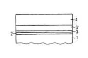
- FIG. 1there is shown part of a silicon wafer with a silicon substrate 1 .
- the state of a silicon wafer that is shown in FIG. 1corresponds, for example, to the state which a silicon wafer adopts in a standard CMOS process after the wells of the CMOS transistors and the isolation (not shown) of the individual transistors have already been produced.
- a silicon dioxide layer 2which is approximately 1 to 5 nm thick, is applied to a surface of the silicon substrate 1 as a barrier layer.
- the oxide layer 2may be produced, for example, by thermal oxidation. If the thermal oxidation is carried out in an atmosphere which additionally contains NO or N 2 O molecules, it is possible to produce a nitrided silicon dioxide layer 2 . Silicon dioxide layers have an extremely low trap density, which has positive effects on the operation of the transistor that is still to be produced.
- a tungsten-containing layer 3is applied to the oxide layer 2 .
- the tungsten-containing layer 3may be a pure tungsten layer, a tungsten nitride layer or a tungsten silicide layer.
- the tungsten-containing layer 3is produced, for example, by a sputtering process (PVD process) or by a chemical vapor deposition (CVD) process.
- the layer thickness of the tungsten-containing layer 3 produced in this wayis approximately 10 to 20 nm.
- the resulting situationis shown in FIG. 2 .
- the tungsten-containing layer 3is converted into a tungsten oxide layer 3 ′ by a thermal oxidation.
- the conversiontakes place in an oxygen atmosphere (for example O 2 or H 2 O) at a temperature of 500 to 1200° C.
- an oxygen atmospherefor example O 2 or H 2 O
- the temperatureshould not exceed approximately 600° C. or what is known as a low thermal budget rapid thermal oxidation (RTO) should be carried out, in order to prevent silicon from diffusing into the tungsten-containing layer 3 and the tungsten-containing layer 3 from being oxidized.
- RTOrapid thermal oxidation
- the thermal oxidation of the tungsten-containing layer 3leads to a tungsten oxide layer 3 ′ which has scarcely any impurities and a relative dielectric constant ( ⁇ r) of greater than 50.
- the layers and the process parametersmay be selected in such a way that the tungsten-containing layer 3 is completely converted into the tungsten oxide layer 3 ′ or that part of the tungsten-containing layer 3 is not oxidized.
- the heat treatmentmay take place immediately after the production of the tungsten oxide layer 3 ′, but may also only be carried out in a later process step during the fabrication of an integrated circuit.
- the layer stack shown in FIG. 3is eminently suitable for use in an MOS transistor since, as has already been mentioned, the silicon dioxide layer 2 (barrier layer) has an extremely low trap density. For a storage dielectric, this is not absolutely necessary, so that for this application it is also possible to dispense with the silicon dioxide layer 2 . Any part of the tungsten-rich layer 3 (for example tungsten nitride) that remains after the thermal oxidation is then responsible for the function of a (conductive) barrier layer. In this way, it is possible to achieve a very high capacitance using a simple and inexpensive procedure.
- FIG. 7A corresponding layer stack containing a conductive tungsten nitride layer 2 (barrier layer and lower electrode), tungsten oxide layer 3 ′ and a conductive tungsten nitride layer 4 (upper electrode) on a silicon substrate 1 is shown in FIG. 7 .
- the conductive layer 4forms, for example, the gate electrode of an MOS transistor and usually consists of doped polysilicon.
- the polysilicon layer 4is structured so that gate tracks 5 are produced.
- the gate tracks 5in turn form a mask for the subsequent etching of the tungsten oxide layer 3 ′.
- a mixture of CF 4 and O 2is used as the etching gas.
- the temperature of the etchingis approximately 250° C.
- the etching gasis excited to form a plasma by the introduction of HF or by microwave excitation.
- the ratio of CF 4 to O 2is approximately 2% to 98%.
- the fluorine that is released and the associated reaction of the tungsten oxide with the fluorineare responsible for the etching itself. Volatile tungsten/fluorine compounds are formed.
- the oxygenacts as a passivator for the (poly)silicon. Oxygen causes the formation of SiO 2 , the bonding energy of which (without the use of additional ion energy) is too high to be etched to any significant extent by the small proportion of fluorine. Therefore, the etching of the tungsten oxide layer takes place highly selectively with respect to (poly)silicon and with respect to silicon oxide. The resulting situation is shown in FIG. 4 .
- the process for producing the transistorcan then be continued in accordance with a standard CMOS process in order to produce the complete transistor. These steps are known per se and consequently require no further explanation.
- FIG. 5shows part of a silicon wafer with the silicon substrate 1 for explaining a second embodiment of the process according to the invention.
- the state of a silicon wafer shown in FIG. 5once again corresponds to the state that a silicon wafer adopts in a standard CMOS process after the wells of the CMOS transistors and the isolation (not shown) of the individual transistors have been produced.
- the tungsten oxide layer 3 ′is applied directly to the silicon substrate 1 .
- the tungsten oxide layer 3 ′is produced by a CVD process.
- tungsten fluoride and waterare guided onto the substrate surface in the gaseous state as precursors: 2WF 6 +4 H 2 O ⁇ (WOF 4 )+WO 3 +(HF) or WF 6 +H 2 O+Si ⁇ W—O+(2HF)+(SiF 4 )
- the heat treatmentmay immediately follow the production of the tungsten oxide layer 3 ′, but may also only be carried out in a subsequent process step during the fabrication of an integrated circuit. The resulting situation is shown in FIG. 5 .
- a conductive layer on the tungsten oxide layer 3 ′is followed by the production of a conductive layer on the tungsten oxide layer 3 ′.
- a further barrier layerfor example a tungsten nitride layer (not shown), to be deposited before the conductive layer.
- the conductive layer and the tungsten oxide 3 ′can then in turn be structured as has already been described in connection with FIG. 4 . The resulting situation is shown in FIG. 6 .
Landscapes
- Engineering & Computer Science (AREA)
- Manufacturing & Machinery (AREA)
- Microelectronics & Electronic Packaging (AREA)
- Computer Hardware Design (AREA)
- Physics & Mathematics (AREA)
- Power Engineering (AREA)
- Condensed Matter Physics & Semiconductors (AREA)
- General Physics & Mathematics (AREA)
- Chemical & Material Sciences (AREA)
- Crystallography & Structural Chemistry (AREA)
- Chemical Kinetics & Catalysis (AREA)
- General Chemical & Material Sciences (AREA)
- Semiconductor Memories (AREA)
- Inorganic Compounds Of Heavy Metals (AREA)
- Physical Vapour Deposition (AREA)
- Electrodes Of Semiconductors (AREA)
- Formation Of Insulating Films (AREA)
- Insulated Gate Type Field-Effect Transistor (AREA)
Abstract
Description
- a) a tungsten-containing layer is provided,
- b) the tungsten-containing layer is thermally oxidized in an oxygen-containing atmosphere, and
- c) the layer of tungsten oxide is subjected to a heat treatment at a temperature of between 550 and 1100° C., preferably 700 to 1100° C., so that a layer of tungsten oxide (WOx) with a relative dielectric constant (∈r) of greater than 50 is produced.
- a) a tungsten-containing layer is provided, and
- b) the tungsten-containing layer is thermally oxidized in an oxygen-containing atmosphere, so that a layer of tungsten oxide (WOx) with a relative dielectric constant (∈r) of greater than 50 is produced.
- a) a surface of the semiconductor component is prepared; and
- b) tungsten fluoride and water are guided onto the surface in the gaseous state, so that a layer of tungsten oxide (WOx) is produced.
- a) a tungsten oxide layer is provided,
- b) a mask is applied to the tungsten oxide layer, and
- c) the tungsten oxide layer is subjected to dry etching in accordance with the mask in an oxidizing atmosphere at a temperature greater than 130° C., the oxidizing atmosphere containing at least one halogen compound, in particular CF4.
- CVD W (on silicon, nonselective)
- e.g. WF6+SiH4→W+gases (seed layer)
- e.g. WF6+H2→W+gases (bulk layer)
- CVD W (on silicon, selective with respect to nitride, oxide):
- e.g. 2
WF 63 Si→2 W+3 (SiF4) - (a process of this type is described by R. V. Joshi et al., in J. Appl.Phys. 71(3) 1 Feb. 1992, pp. 1428)
- e.g. WF6+H2→W+gases
- e.g. 2
- CVD WSix:
- e.g. WF6+SiH2Cl2→WSix(e.g. x=2-3)+gases
- (likewise R. V. Joshi et al., J. Appl.Phys. 71(3) 1 Feb. 1992, pp. 1428)
- CVD WN (tungsten nitride, e.g. W2N):
- e.g. 4 WF6+N2+12H2(Plasma CVD)→4 W2N+24 (HF)
- (e.g. at a temperature of 350-400° C.)
2WF6+4 H2O→(WOF4)+WO3+(HF) or
WF6+H2O+Si→W—O+(2HF)+(SiF4)
Claims (6)
Applications Claiming Priority (3)
| Application Number | Priority Date | Filing Date | Title |
|---|---|---|---|
| DE19901210ADE19901210A1 (en) | 1999-01-14 | 1999-01-14 | Semiconductor component and method for its production |
| DE19901210.5 | 1999-01-14 | ||
| PCT/DE2000/000047WO2000041459A2 (en) | 1999-01-14 | 2000-01-05 | Semiconductor element with a tungsten oxide layer and method for its production |
Related Parent Applications (1)
| Application Number | Title | Priority Date | Filing Date |
|---|---|---|---|
| PCT/DE2000/000047ContinuationWO2000041459A2 (en) | 1999-01-14 | 2000-01-05 | Semiconductor element with a tungsten oxide layer and method for its production |
Publications (2)
| Publication Number | Publication Date |
|---|---|
| US20020070414A1 US20020070414A1 (en) | 2002-06-13 |
| US6960541B2true US6960541B2 (en) | 2005-11-01 |
Family
ID=7894251
Family Applications (1)
| Application Number | Title | Priority Date | Filing Date |
|---|---|---|---|
| US09/906,338Expired - Fee RelatedUS6960541B2 (en) | 1999-01-14 | 2001-07-16 | Process for fabrication of a semiconductor component having a tungsten oxide layer |
Country Status (8)
| Country | Link |
|---|---|
| US (1) | US6960541B2 (en) |
| EP (1) | EP1145279B1 (en) |
| JP (1) | JP2002534818A (en) |
| KR (1) | KR100703260B1 (en) |
| CN (1) | CN100355085C (en) |
| DE (2) | DE19901210A1 (en) |
| TW (1) | TW478165B (en) |
| WO (1) | WO2000041459A2 (en) |
Families Citing this family (150)
| Publication number | Priority date | Publication date | Assignee | Title |
|---|---|---|---|---|
| DE19944012B4 (en) | 1999-09-14 | 2007-07-19 | Infineon Technologies Ag | Trench capacitor with capacitor electrodes and corresponding manufacturing process |
| US7491642B2 (en) | 2000-07-12 | 2009-02-17 | The California Institute Of Technology | Electrical passivation of silicon-containing surfaces using organic layers |
| DE10043731C2 (en) | 2000-09-05 | 2003-06-26 | Infineon Technologies Ag | Measuring probe, its use and manufacture and measuring system for detecting electrical signals in an integrated semiconductor circuit |
| DE10054936C1 (en)* | 2000-11-06 | 2002-04-25 | Infineon Technologies Ag | Production of an integrated circuit comprises forming metallizing regions in a substrate, applying an intermediate layer, removing the layer to form an oxide film, and partially converting the oxide film to produce a conducting connection |
| US7378719B2 (en) | 2000-12-20 | 2008-05-27 | Micron Technology, Inc. | Low leakage MIM capacitor |
| CN100573953C (en)* | 2006-10-13 | 2009-12-23 | 旺宏电子股份有限公司 | Operation method of resistive memory element |
| CN101159284B (en)* | 2007-09-13 | 2010-09-29 | 复旦大学 | A kind of self-aligned WOX resistance memory with upper electrode formed and its manufacturing method |
| CN101826595B (en)* | 2009-03-03 | 2013-02-27 | 复旦大学 | A WOx-based resistive memory and its preparation method |
| CN102169956B (en)* | 2010-02-25 | 2013-04-17 | 复旦大学 | WOx-based resistive memory and preparation method thereof |
| US9324576B2 (en) | 2010-05-27 | 2016-04-26 | Applied Materials, Inc. | Selective etch for silicon films |
| US10283321B2 (en) | 2011-01-18 | 2019-05-07 | Applied Materials, Inc. | Semiconductor processing system and methods using capacitively coupled plasma |
| US9064815B2 (en) | 2011-03-14 | 2015-06-23 | Applied Materials, Inc. | Methods for etch of metal and metal-oxide films |
| US8999856B2 (en) | 2011-03-14 | 2015-04-07 | Applied Materials, Inc. | Methods for etch of sin films |
| US8771536B2 (en) | 2011-08-01 | 2014-07-08 | Applied Materials, Inc. | Dry-etch for silicon-and-carbon-containing films |
| US8808563B2 (en) | 2011-10-07 | 2014-08-19 | Applied Materials, Inc. | Selective etch of silicon by way of metastable hydrogen termination |
| US9267739B2 (en) | 2012-07-18 | 2016-02-23 | Applied Materials, Inc. | Pedestal with multi-zone temperature control and multiple purge capabilities |
| US9373517B2 (en) | 2012-08-02 | 2016-06-21 | Applied Materials, Inc. | Semiconductor processing with DC assisted RF power for improved control |
| US9034770B2 (en) | 2012-09-17 | 2015-05-19 | Applied Materials, Inc. | Differential silicon oxide etch |
| US9023734B2 (en) | 2012-09-18 | 2015-05-05 | Applied Materials, Inc. | Radical-component oxide etch |
| US9390937B2 (en) | 2012-09-20 | 2016-07-12 | Applied Materials, Inc. | Silicon-carbon-nitride selective etch |
| US9132436B2 (en) | 2012-09-21 | 2015-09-15 | Applied Materials, Inc. | Chemical control features in wafer process equipment |
| US8969212B2 (en) | 2012-11-20 | 2015-03-03 | Applied Materials, Inc. | Dry-etch selectivity |
| US8980763B2 (en) | 2012-11-30 | 2015-03-17 | Applied Materials, Inc. | Dry-etch for selective tungsten removal |
| US9064816B2 (en)* | 2012-11-30 | 2015-06-23 | Applied Materials, Inc. | Dry-etch for selective oxidation removal |
| US9111877B2 (en) | 2012-12-18 | 2015-08-18 | Applied Materials, Inc. | Non-local plasma oxide etch |
| US8921234B2 (en) | 2012-12-21 | 2014-12-30 | Applied Materials, Inc. | Selective titanium nitride etching |
| US10256079B2 (en) | 2013-02-08 | 2019-04-09 | Applied Materials, Inc. | Semiconductor processing systems having multiple plasma configurations |
| US9362130B2 (en) | 2013-03-01 | 2016-06-07 | Applied Materials, Inc. | Enhanced etching processes using remote plasma sources |
| US9040422B2 (en) | 2013-03-05 | 2015-05-26 | Applied Materials, Inc. | Selective titanium nitride removal |
| US10170282B2 (en) | 2013-03-08 | 2019-01-01 | Applied Materials, Inc. | Insulated semiconductor faceplate designs |
| US20140271097A1 (en) | 2013-03-15 | 2014-09-18 | Applied Materials, Inc. | Processing systems and methods for halide scavenging |
| US9493879B2 (en) | 2013-07-12 | 2016-11-15 | Applied Materials, Inc. | Selective sputtering for pattern transfer |
| US9773648B2 (en) | 2013-08-30 | 2017-09-26 | Applied Materials, Inc. | Dual discharge modes operation for remote plasma |
| US8956980B1 (en) | 2013-09-16 | 2015-02-17 | Applied Materials, Inc. | Selective etch of silicon nitride |
| US9236265B2 (en) | 2013-11-04 | 2016-01-12 | Applied Materials, Inc. | Silicon germanium processing |
| US9576809B2 (en) | 2013-11-04 | 2017-02-21 | Applied Materials, Inc. | Etch suppression with germanium |
| US9520303B2 (en) | 2013-11-12 | 2016-12-13 | Applied Materials, Inc. | Aluminum selective etch |
| US9245762B2 (en) | 2013-12-02 | 2016-01-26 | Applied Materials, Inc. | Procedure for etch rate consistency |
| US9117855B2 (en) | 2013-12-04 | 2015-08-25 | Applied Materials, Inc. | Polarity control for remote plasma |
| US9263278B2 (en) | 2013-12-17 | 2016-02-16 | Applied Materials, Inc. | Dopant etch selectivity control |
| US9287095B2 (en) | 2013-12-17 | 2016-03-15 | Applied Materials, Inc. | Semiconductor system assemblies and methods of operation |
| US9190293B2 (en) | 2013-12-18 | 2015-11-17 | Applied Materials, Inc. | Even tungsten etch for high aspect ratio trenches |
| US9287134B2 (en) | 2014-01-17 | 2016-03-15 | Applied Materials, Inc. | Titanium oxide etch |
| US9293568B2 (en) | 2014-01-27 | 2016-03-22 | Applied Materials, Inc. | Method of fin patterning |
| US9396989B2 (en) | 2014-01-27 | 2016-07-19 | Applied Materials, Inc. | Air gaps between copper lines |
| US9385028B2 (en) | 2014-02-03 | 2016-07-05 | Applied Materials, Inc. | Air gap process |
| US9499898B2 (en) | 2014-03-03 | 2016-11-22 | Applied Materials, Inc. | Layered thin film heater and method of fabrication |
| US9299575B2 (en) | 2014-03-17 | 2016-03-29 | Applied Materials, Inc. | Gas-phase tungsten etch |
| US9299538B2 (en) | 2014-03-20 | 2016-03-29 | Applied Materials, Inc. | Radial waveguide systems and methods for post-match control of microwaves |
| US9299537B2 (en) | 2014-03-20 | 2016-03-29 | Applied Materials, Inc. | Radial waveguide systems and methods for post-match control of microwaves |
| US9136273B1 (en) | 2014-03-21 | 2015-09-15 | Applied Materials, Inc. | Flash gate air gap |
| US9903020B2 (en) | 2014-03-31 | 2018-02-27 | Applied Materials, Inc. | Generation of compact alumina passivation layers on aluminum plasma equipment components |
| US9269590B2 (en) | 2014-04-07 | 2016-02-23 | Applied Materials, Inc. | Spacer formation |
| US9309598B2 (en) | 2014-05-28 | 2016-04-12 | Applied Materials, Inc. | Oxide and metal removal |
| US9847289B2 (en) | 2014-05-30 | 2017-12-19 | Applied Materials, Inc. | Protective via cap for improved interconnect performance |
| US9406523B2 (en) | 2014-06-19 | 2016-08-02 | Applied Materials, Inc. | Highly selective doped oxide removal method |
| US9378969B2 (en) | 2014-06-19 | 2016-06-28 | Applied Materials, Inc. | Low temperature gas-phase carbon removal |
| US9425058B2 (en) | 2014-07-24 | 2016-08-23 | Applied Materials, Inc. | Simplified litho-etch-litho-etch process |
| US9496167B2 (en) | 2014-07-31 | 2016-11-15 | Applied Materials, Inc. | Integrated bit-line airgap formation and gate stack post clean |
| US9378978B2 (en) | 2014-07-31 | 2016-06-28 | Applied Materials, Inc. | Integrated oxide recess and floating gate fin trimming |
| US9159606B1 (en) | 2014-07-31 | 2015-10-13 | Applied Materials, Inc. | Metal air gap |
| US9165786B1 (en) | 2014-08-05 | 2015-10-20 | Applied Materials, Inc. | Integrated oxide and nitride recess for better channel contact in 3D architectures |
| US9659753B2 (en) | 2014-08-07 | 2017-05-23 | Applied Materials, Inc. | Grooved insulator to reduce leakage current |
| US9553102B2 (en) | 2014-08-19 | 2017-01-24 | Applied Materials, Inc. | Tungsten separation |
| US9355856B2 (en) | 2014-09-12 | 2016-05-31 | Applied Materials, Inc. | V trench dry etch |
| US9355862B2 (en) | 2014-09-24 | 2016-05-31 | Applied Materials, Inc. | Fluorine-based hardmask removal |
| US9368364B2 (en) | 2014-09-24 | 2016-06-14 | Applied Materials, Inc. | Silicon etch process with tunable selectivity to SiO2 and other materials |
| US9613822B2 (en) | 2014-09-25 | 2017-04-04 | Applied Materials, Inc. | Oxide etch selectivity enhancement |
| US9355922B2 (en) | 2014-10-14 | 2016-05-31 | Applied Materials, Inc. | Systems and methods for internal surface conditioning in plasma processing equipment |
| US9966240B2 (en) | 2014-10-14 | 2018-05-08 | Applied Materials, Inc. | Systems and methods for internal surface conditioning assessment in plasma processing equipment |
| US11637002B2 (en) | 2014-11-26 | 2023-04-25 | Applied Materials, Inc. | Methods and systems to enhance process uniformity |
| US9299583B1 (en) | 2014-12-05 | 2016-03-29 | Applied Materials, Inc. | Aluminum oxide selective etch |
| US10573496B2 (en) | 2014-12-09 | 2020-02-25 | Applied Materials, Inc. | Direct outlet toroidal plasma source |
| US10224210B2 (en) | 2014-12-09 | 2019-03-05 | Applied Materials, Inc. | Plasma processing system with direct outlet toroidal plasma source |
| US9502258B2 (en) | 2014-12-23 | 2016-11-22 | Applied Materials, Inc. | Anisotropic gap etch |
| US9343272B1 (en) | 2015-01-08 | 2016-05-17 | Applied Materials, Inc. | Self-aligned process |
| US11257693B2 (en) | 2015-01-09 | 2022-02-22 | Applied Materials, Inc. | Methods and systems to improve pedestal temperature control |
| US9373522B1 (en) | 2015-01-22 | 2016-06-21 | Applied Mateials, Inc. | Titanium nitride removal |
| US9449846B2 (en) | 2015-01-28 | 2016-09-20 | Applied Materials, Inc. | Vertical gate separation |
| US9728437B2 (en) | 2015-02-03 | 2017-08-08 | Applied Materials, Inc. | High temperature chuck for plasma processing systems |
| US20160225652A1 (en) | 2015-02-03 | 2016-08-04 | Applied Materials, Inc. | Low temperature chuck for plasma processing systems |
| US9881805B2 (en) | 2015-03-02 | 2018-01-30 | Applied Materials, Inc. | Silicon selective removal |
| US9691645B2 (en) | 2015-08-06 | 2017-06-27 | Applied Materials, Inc. | Bolted wafer chuck thermal management systems and methods for wafer processing systems |
| US9741593B2 (en) | 2015-08-06 | 2017-08-22 | Applied Materials, Inc. | Thermal management systems and methods for wafer processing systems |
| US9349605B1 (en) | 2015-08-07 | 2016-05-24 | Applied Materials, Inc. | Oxide etch selectivity systems and methods |
| US10504700B2 (en) | 2015-08-27 | 2019-12-10 | Applied Materials, Inc. | Plasma etching systems and methods with secondary plasma injection |
| US10522371B2 (en) | 2016-05-19 | 2019-12-31 | Applied Materials, Inc. | Systems and methods for improved semiconductor etching and component protection |
| US10504754B2 (en) | 2016-05-19 | 2019-12-10 | Applied Materials, Inc. | Systems and methods for improved semiconductor etching and component protection |
| US9865484B1 (en) | 2016-06-29 | 2018-01-09 | Applied Materials, Inc. | Selective etch using material modification and RF pulsing |
| US10062575B2 (en) | 2016-09-09 | 2018-08-28 | Applied Materials, Inc. | Poly directional etch by oxidation |
| US10629473B2 (en) | 2016-09-09 | 2020-04-21 | Applied Materials, Inc. | Footing removal for nitride spacer |
| US9721789B1 (en) | 2016-10-04 | 2017-08-01 | Applied Materials, Inc. | Saving ion-damaged spacers |
| US10546729B2 (en) | 2016-10-04 | 2020-01-28 | Applied Materials, Inc. | Dual-channel showerhead with improved profile |
| US10062585B2 (en) | 2016-10-04 | 2018-08-28 | Applied Materials, Inc. | Oxygen compatible plasma source |
| US9934942B1 (en) | 2016-10-04 | 2018-04-03 | Applied Materials, Inc. | Chamber with flow-through source |
| US10062579B2 (en) | 2016-10-07 | 2018-08-28 | Applied Materials, Inc. | Selective SiN lateral recess |
| US9947549B1 (en) | 2016-10-10 | 2018-04-17 | Applied Materials, Inc. | Cobalt-containing material removal |
| US10163696B2 (en) | 2016-11-11 | 2018-12-25 | Applied Materials, Inc. | Selective cobalt removal for bottom up gapfill |
| US9768034B1 (en) | 2016-11-11 | 2017-09-19 | Applied Materials, Inc. | Removal methods for high aspect ratio structures |
| US10026621B2 (en) | 2016-11-14 | 2018-07-17 | Applied Materials, Inc. | SiN spacer profile patterning |
| US10242908B2 (en) | 2016-11-14 | 2019-03-26 | Applied Materials, Inc. | Airgap formation with damage-free copper |
| US10566206B2 (en) | 2016-12-27 | 2020-02-18 | Applied Materials, Inc. | Systems and methods for anisotropic material breakthrough |
| US10403507B2 (en) | 2017-02-03 | 2019-09-03 | Applied Materials, Inc. | Shaped etch profile with oxidation |
| US10431429B2 (en) | 2017-02-03 | 2019-10-01 | Applied Materials, Inc. | Systems and methods for radial and azimuthal control of plasma uniformity |
| US10043684B1 (en) | 2017-02-06 | 2018-08-07 | Applied Materials, Inc. | Self-limiting atomic thermal etching systems and methods |
| US10319739B2 (en) | 2017-02-08 | 2019-06-11 | Applied Materials, Inc. | Accommodating imperfectly aligned memory holes |
| US10943834B2 (en) | 2017-03-13 | 2021-03-09 | Applied Materials, Inc. | Replacement contact process |
| US10319649B2 (en) | 2017-04-11 | 2019-06-11 | Applied Materials, Inc. | Optical emission spectroscopy (OES) for remote plasma monitoring |
| US11276590B2 (en) | 2017-05-17 | 2022-03-15 | Applied Materials, Inc. | Multi-zone semiconductor substrate supports |
| US11276559B2 (en) | 2017-05-17 | 2022-03-15 | Applied Materials, Inc. | Semiconductor processing chamber for multiple precursor flow |
| JP7176860B6 (en) | 2017-05-17 | 2022-12-16 | アプライド マテリアルズ インコーポレイテッド | Semiconductor processing chamber to improve precursor flow |
| US10497579B2 (en) | 2017-05-31 | 2019-12-03 | Applied Materials, Inc. | Water-free etching methods |
| US10049891B1 (en) | 2017-05-31 | 2018-08-14 | Applied Materials, Inc. | Selective in situ cobalt residue removal |
| US10920320B2 (en) | 2017-06-16 | 2021-02-16 | Applied Materials, Inc. | Plasma health determination in semiconductor substrate processing reactors |
| US10541246B2 (en) | 2017-06-26 | 2020-01-21 | Applied Materials, Inc. | 3D flash memory cells which discourage cross-cell electrical tunneling |
| US10727080B2 (en) | 2017-07-07 | 2020-07-28 | Applied Materials, Inc. | Tantalum-containing material removal |
| US10541184B2 (en) | 2017-07-11 | 2020-01-21 | Applied Materials, Inc. | Optical emission spectroscopic techniques for monitoring etching |
| US10354889B2 (en) | 2017-07-17 | 2019-07-16 | Applied Materials, Inc. | Non-halogen etching of silicon-containing materials |
| US10170336B1 (en) | 2017-08-04 | 2019-01-01 | Applied Materials, Inc. | Methods for anisotropic control of selective silicon removal |
| US10043674B1 (en) | 2017-08-04 | 2018-08-07 | Applied Materials, Inc. | Germanium etching systems and methods |
| US10297458B2 (en) | 2017-08-07 | 2019-05-21 | Applied Materials, Inc. | Process window widening using coated parts in plasma etch processes |
| US10128086B1 (en) | 2017-10-24 | 2018-11-13 | Applied Materials, Inc. | Silicon pretreatment for nitride removal |
| US10283324B1 (en) | 2017-10-24 | 2019-05-07 | Applied Materials, Inc. | Oxygen treatment for nitride etching |
| US10256112B1 (en) | 2017-12-08 | 2019-04-09 | Applied Materials, Inc. | Selective tungsten removal |
| US10903054B2 (en) | 2017-12-19 | 2021-01-26 | Applied Materials, Inc. | Multi-zone gas distribution systems and methods |
| US11328909B2 (en) | 2017-12-22 | 2022-05-10 | Applied Materials, Inc. | Chamber conditioning and removal processes |
| US10854426B2 (en) | 2018-01-08 | 2020-12-01 | Applied Materials, Inc. | Metal recess for semiconductor structures |
| US10679870B2 (en) | 2018-02-15 | 2020-06-09 | Applied Materials, Inc. | Semiconductor processing chamber multistage mixing apparatus |
| US10964512B2 (en) | 2018-02-15 | 2021-03-30 | Applied Materials, Inc. | Semiconductor processing chamber multistage mixing apparatus and methods |
| TWI766433B (en) | 2018-02-28 | 2022-06-01 | 美商應用材料股份有限公司 | Systems and methods to form airgaps |
| US10593560B2 (en) | 2018-03-01 | 2020-03-17 | Applied Materials, Inc. | Magnetic induction plasma source for semiconductor processes and equipment |
| US10319600B1 (en) | 2018-03-12 | 2019-06-11 | Applied Materials, Inc. | Thermal silicon etch |
| US10497573B2 (en) | 2018-03-13 | 2019-12-03 | Applied Materials, Inc. | Selective atomic layer etching of semiconductor materials |
| US10573527B2 (en) | 2018-04-06 | 2020-02-25 | Applied Materials, Inc. | Gas-phase selective etching systems and methods |
| US10490406B2 (en) | 2018-04-10 | 2019-11-26 | Appled Materials, Inc. | Systems and methods for material breakthrough |
| US10699879B2 (en) | 2018-04-17 | 2020-06-30 | Applied Materials, Inc. | Two piece electrode assembly with gap for plasma control |
| US10886137B2 (en) | 2018-04-30 | 2021-01-05 | Applied Materials, Inc. | Selective nitride removal |
| US10872778B2 (en) | 2018-07-06 | 2020-12-22 | Applied Materials, Inc. | Systems and methods utilizing solid-phase etchants |
| US10755941B2 (en) | 2018-07-06 | 2020-08-25 | Applied Materials, Inc. | Self-limiting selective etching systems and methods |
| US10672642B2 (en) | 2018-07-24 | 2020-06-02 | Applied Materials, Inc. | Systems and methods for pedestal configuration |
| US11049755B2 (en) | 2018-09-14 | 2021-06-29 | Applied Materials, Inc. | Semiconductor substrate supports with embedded RF shield |
| US10892198B2 (en) | 2018-09-14 | 2021-01-12 | Applied Materials, Inc. | Systems and methods for improved performance in semiconductor processing |
| US11062887B2 (en) | 2018-09-17 | 2021-07-13 | Applied Materials, Inc. | High temperature RF heater pedestals |
| US11417534B2 (en) | 2018-09-21 | 2022-08-16 | Applied Materials, Inc. | Selective material removal |
| US11682560B2 (en) | 2018-10-11 | 2023-06-20 | Applied Materials, Inc. | Systems and methods for hafnium-containing film removal |
| US11121002B2 (en) | 2018-10-24 | 2021-09-14 | Applied Materials, Inc. | Systems and methods for etching metals and metal derivatives |
| US11437242B2 (en) | 2018-11-27 | 2022-09-06 | Applied Materials, Inc. | Selective removal of silicon-containing materials |
| US11721527B2 (en) | 2019-01-07 | 2023-08-08 | Applied Materials, Inc. | Processing chamber mixing systems |
| US10920319B2 (en) | 2019-01-11 | 2021-02-16 | Applied Materials, Inc. | Ceramic showerheads with conductive electrodes |
| CN111977629A (en)* | 2019-05-21 | 2020-11-24 | 中国科学院宁波材料技术与工程研究所 | Synthetic method for coating carbon spheres with tungsten nitride and generating tungsten nitride nanorods in situ on carbon spheres |
Citations (30)
| Publication number | Priority date | Publication date | Assignee | Title |
|---|---|---|---|---|
| US4377734A (en)* | 1979-10-13 | 1983-03-22 | Mitsubishi Denki Kabushiki Kaisha | Method for forming patterns by plasma etching |
| US4505028A (en)* | 1983-01-19 | 1985-03-19 | Hitachi, Ltd. | Method of producing semiconductor device |
| US4522936A (en)* | 1983-03-21 | 1985-06-11 | Phillips Petroleum Company | Metathesis catalyst |
| US4965594A (en)* | 1986-02-28 | 1990-10-23 | Canon Kabushiki Kaisha | Liquid jet recording head with laminated heat resistive layers on a support member |
| EP0418540A2 (en) | 1989-08-11 | 1991-03-27 | Sanyo Electric Co., Ltd | Dry etching method |
| US5075251A (en)* | 1988-09-09 | 1991-12-24 | L'etat Francais | Tungsten silicide self-aligned formation process |
| US5089432A (en)* | 1990-08-17 | 1992-02-18 | Taiwan Semiconductor Manufacturing Company | Polycide gate MOSFET process for integrated circuits |
| KR920010669A (en) | 1990-11-20 | 1992-06-27 | 서주인 | Manufacturing method of rare earth-iron magnet |
| US5189503A (en)* | 1988-03-04 | 1993-02-23 | Kabushiki Kaisha Toshiba | High dielectric capacitor having low current leakage |
| KR940002740A (en) | 1992-07-02 | 1994-02-19 | 이희종 | Raw material hardening prevention device of beverage vending machine |
| US5348894A (en)* | 1993-01-27 | 1994-09-20 | Texas Instruments Incorporated | Method of forming electrical connections to high dielectric constant materials |
| US5358899A (en)* | 1991-10-25 | 1994-10-25 | International Business Machines Corporation | Oxygen assisted ohmic contact formation to n-type gallium arsenide |
| JPH07135202A (en) | 1993-11-09 | 1995-05-23 | Miyagi Oki Denki Kk | Manufacture of semiconductor device |
| US5444011A (en)* | 1991-10-18 | 1995-08-22 | Sharp Kabushiki Kaisha | Method for forming a thin film capacitive memory deivce with a high dielectric constant |
| US5541131A (en)* | 1991-02-01 | 1996-07-30 | Taiwan Semiconductor Manufacturing Co. | Peeling free metal silicide films using ion implantation |
| US5650041A (en)* | 1994-06-17 | 1997-07-22 | Texas Instruments Incorporated | Semiconductor device fabrication method |
| US5744832A (en)* | 1994-10-04 | 1998-04-28 | U.S. Philips Corporation | Semiconductor device having a ferroelectric memory element with a lower electrode provided with an oxygen barrier |
| US6001718A (en)* | 1997-09-30 | 1999-12-14 | Kabushiki Kaisha Toshiba | Semiconductor device having a ternary compound low resistive electrode |
| US6140167A (en)* | 1998-08-18 | 2000-10-31 | Advanced Micro Devices, Inc. | High performance MOSFET and method of forming the same using silicidation and junction implantation prior to gate formation |
| US6162717A (en)* | 1998-06-19 | 2000-12-19 | Promos Technologies, Inc | Method of manufacturing MOS gate utilizing a nitridation reaction |
| US6162741A (en)* | 1996-12-03 | 2000-12-19 | Kabushiki Kaisha Toshiba | Semiconductor device and manufacturing method therefor |
| US6168958B1 (en)* | 1998-08-07 | 2001-01-02 | Advanced Micro Devices Inc. | Semiconductor structure having multiple thicknesses of high-K gate dielectrics and process of manufacture therefor |
| US6180481B1 (en)* | 1998-01-09 | 2001-01-30 | Micron Technology, Inc. | Barrier layer fabrication methods |
| US6204203B1 (en)* | 1998-10-14 | 2001-03-20 | Applied Materials, Inc. | Post deposition treatment of dielectric films for interface control |
| US6222214B1 (en)* | 1995-04-27 | 2001-04-24 | Taiwan Semiconductor Manufacturing Company | Plug structure and process for forming stacked contacts and metal contacts on static random access memory thin film transistors |
| US6281126B1 (en)* | 1998-03-16 | 2001-08-28 | Oki Electronic Industry Co., Ltd. | Process for manufacturing semiconductor device |
| US6284646B1 (en)* | 1997-08-19 | 2001-09-04 | Samsung Electronics Co., Ltd | Methods of forming smooth conductive layers for integrated circuit devices |
| US6291868B1 (en)* | 1998-02-26 | 2001-09-18 | Micron Technology, Inc. | Forming a conductive structure in a semiconductor device |
| US6498097B1 (en)* | 1997-05-06 | 2002-12-24 | Tong Yang Cement Corporation | Apparatus and method of forming preferred orientation-controlled platinum film using oxygen |
| US6635523B1 (en)* | 1997-12-04 | 2003-10-21 | Fujitsu Limited | Semiconductor device and method of manufacturing the same |
Family Cites Families (7)
| Publication number | Priority date | Publication date | Assignee | Title |
|---|---|---|---|---|
| US5420060A (en)* | 1988-11-14 | 1995-05-30 | Texas Instruments Incorporated | Method of making contract-free floating-gate memory array with silicided buried bitlines and with single-step defined floating gates |
| JP3047256B2 (en)* | 1991-06-13 | 2000-05-29 | 株式会社豊田中央研究所 | Dielectric thin film |
| CA2074848C (en)* | 1992-07-29 | 1998-02-10 | Joseph P. Ellul | Method of forming electrodes for trench capacitors |
| JPH0758290A (en)* | 1993-08-09 | 1995-03-03 | Asahi Chem Ind Co Ltd | Manufacture of semiconductor device |
| JP3398439B2 (en)* | 1993-11-22 | 2003-04-21 | 三井化学株式会社 | Method for producing poly-α-olefin |
| US6034896A (en)* | 1995-07-03 | 2000-03-07 | The University Of Toronto, Innovations Foundation | Method of fabricating a fast programmable flash E2 PROM cell |
| US5830575A (en)* | 1996-09-16 | 1998-11-03 | Sandia National Laboratories | Memory device using movement of protons |
- 1999
- 1999-01-14DEDE19901210Apatent/DE19901210A1/ennot_activeWithdrawn
- 2000
- 2000-01-05EPEP00902538Apatent/EP1145279B1/ennot_activeExpired - Lifetime
- 2000-01-05DEDE50015090Tpatent/DE50015090D1/ennot_activeExpired - Lifetime
- 2000-01-05KRKR1020017008873Apatent/KR100703260B1/ennot_activeExpired - Fee Related
- 2000-01-05CNCNB008050295Apatent/CN100355085C/ennot_activeExpired - Fee Related
- 2000-01-05WOPCT/DE2000/000047patent/WO2000041459A2/enactiveIP Right Grant
- 2000-01-05JPJP2000593084Apatent/JP2002534818A/enactivePending
- 2000-01-11TWTW089100324Apatent/TW478165B/ennot_activeIP Right Cessation
- 2001
- 2001-07-16USUS09/906,338patent/US6960541B2/ennot_activeExpired - Fee Related
Patent Citations (30)
| Publication number | Priority date | Publication date | Assignee | Title |
|---|---|---|---|---|
| US4377734A (en)* | 1979-10-13 | 1983-03-22 | Mitsubishi Denki Kabushiki Kaisha | Method for forming patterns by plasma etching |
| US4505028A (en)* | 1983-01-19 | 1985-03-19 | Hitachi, Ltd. | Method of producing semiconductor device |
| US4522936A (en)* | 1983-03-21 | 1985-06-11 | Phillips Petroleum Company | Metathesis catalyst |
| US4965594A (en)* | 1986-02-28 | 1990-10-23 | Canon Kabushiki Kaisha | Liquid jet recording head with laminated heat resistive layers on a support member |
| US5189503A (en)* | 1988-03-04 | 1993-02-23 | Kabushiki Kaisha Toshiba | High dielectric capacitor having low current leakage |
| US5075251A (en)* | 1988-09-09 | 1991-12-24 | L'etat Francais | Tungsten silicide self-aligned formation process |
| EP0418540A2 (en) | 1989-08-11 | 1991-03-27 | Sanyo Electric Co., Ltd | Dry etching method |
| US5089432A (en)* | 1990-08-17 | 1992-02-18 | Taiwan Semiconductor Manufacturing Company | Polycide gate MOSFET process for integrated circuits |
| KR920010669A (en) | 1990-11-20 | 1992-06-27 | 서주인 | Manufacturing method of rare earth-iron magnet |
| US5541131A (en)* | 1991-02-01 | 1996-07-30 | Taiwan Semiconductor Manufacturing Co. | Peeling free metal silicide films using ion implantation |
| US5444011A (en)* | 1991-10-18 | 1995-08-22 | Sharp Kabushiki Kaisha | Method for forming a thin film capacitive memory deivce with a high dielectric constant |
| US5358899A (en)* | 1991-10-25 | 1994-10-25 | International Business Machines Corporation | Oxygen assisted ohmic contact formation to n-type gallium arsenide |
| KR940002740A (en) | 1992-07-02 | 1994-02-19 | 이희종 | Raw material hardening prevention device of beverage vending machine |
| US5348894A (en)* | 1993-01-27 | 1994-09-20 | Texas Instruments Incorporated | Method of forming electrical connections to high dielectric constant materials |
| JPH07135202A (en) | 1993-11-09 | 1995-05-23 | Miyagi Oki Denki Kk | Manufacture of semiconductor device |
| US5650041A (en)* | 1994-06-17 | 1997-07-22 | Texas Instruments Incorporated | Semiconductor device fabrication method |
| US5744832A (en)* | 1994-10-04 | 1998-04-28 | U.S. Philips Corporation | Semiconductor device having a ferroelectric memory element with a lower electrode provided with an oxygen barrier |
| US6222214B1 (en)* | 1995-04-27 | 2001-04-24 | Taiwan Semiconductor Manufacturing Company | Plug structure and process for forming stacked contacts and metal contacts on static random access memory thin film transistors |
| US6162741A (en)* | 1996-12-03 | 2000-12-19 | Kabushiki Kaisha Toshiba | Semiconductor device and manufacturing method therefor |
| US6498097B1 (en)* | 1997-05-06 | 2002-12-24 | Tong Yang Cement Corporation | Apparatus and method of forming preferred orientation-controlled platinum film using oxygen |
| US6284646B1 (en)* | 1997-08-19 | 2001-09-04 | Samsung Electronics Co., Ltd | Methods of forming smooth conductive layers for integrated circuit devices |
| US6001718A (en)* | 1997-09-30 | 1999-12-14 | Kabushiki Kaisha Toshiba | Semiconductor device having a ternary compound low resistive electrode |
| US6635523B1 (en)* | 1997-12-04 | 2003-10-21 | Fujitsu Limited | Semiconductor device and method of manufacturing the same |
| US6180481B1 (en)* | 1998-01-09 | 2001-01-30 | Micron Technology, Inc. | Barrier layer fabrication methods |
| US6291868B1 (en)* | 1998-02-26 | 2001-09-18 | Micron Technology, Inc. | Forming a conductive structure in a semiconductor device |
| US6281126B1 (en)* | 1998-03-16 | 2001-08-28 | Oki Electronic Industry Co., Ltd. | Process for manufacturing semiconductor device |
| US6162717A (en)* | 1998-06-19 | 2000-12-19 | Promos Technologies, Inc | Method of manufacturing MOS gate utilizing a nitridation reaction |
| US6168958B1 (en)* | 1998-08-07 | 2001-01-02 | Advanced Micro Devices Inc. | Semiconductor structure having multiple thicknesses of high-K gate dielectrics and process of manufacture therefor |
| US6140167A (en)* | 1998-08-18 | 2000-10-31 | Advanced Micro Devices, Inc. | High performance MOSFET and method of forming the same using silicidation and junction implantation prior to gate formation |
| US6204203B1 (en)* | 1998-10-14 | 2001-03-20 | Applied Materials, Inc. | Post deposition treatment of dielectric films for interface control |
Also Published As
| Publication number | Publication date |
|---|---|
| WO2000041459A3 (en) | 2001-05-10 |
| KR100703260B1 (en) | 2007-04-03 |
| DE19901210A1 (en) | 2000-07-27 |
| EP1145279B1 (en) | 2008-04-09 |
| CN1364317A (en) | 2002-08-14 |
| KR20010101512A (en) | 2001-11-14 |
| CN100355085C (en) | 2007-12-12 |
| US20020070414A1 (en) | 2002-06-13 |
| WO2000041459A2 (en) | 2000-07-20 |
| JP2002534818A (en) | 2002-10-15 |
| DE50015090D1 (en) | 2008-05-21 |
| EP1145279A2 (en) | 2001-10-17 |
| TW478165B (en) | 2002-03-01 |
Similar Documents
| Publication | Publication Date | Title |
|---|---|---|
| US6960541B2 (en) | Process for fabrication of a semiconductor component having a tungsten oxide layer | |
| US7323738B2 (en) | MIS capacitor and method of formation | |
| EP0696051B1 (en) | Method for fabricating oxide layer in semiconductor technology | |
| US6656789B2 (en) | Capacitor for highly-integrated semiconductor memory devices and a method for manufacturing the same | |
| US6673668B2 (en) | Method of forming capacitor of a semiconductor memory device | |
| US6287910B2 (en) | Method for forming a capacitor using tantalum nitride as a capacitor dielectric | |
| US6573197B2 (en) | Thermally stable poly-Si/high dielectric constant material interfaces | |
| US7364965B2 (en) | Semiconductor device and method of fabrication | |
| US20040137678A1 (en) | Method for forming capacitor of semiconductor device | |
| US6781180B1 (en) | Trench capacitor and method for fabricating the same | |
| US6525364B1 (en) | Capacitor for semiconductor memory device and method of manufacturing the same | |
| US6740553B1 (en) | Capacitor for semiconductor memory device and method of manufacturing the same | |
| KR100497142B1 (en) | Method of manufacturing a capacitor in a semiconductor device | |
| US20040077142A1 (en) | Atomic layer deposition and plasma treatment method for forming microelectronic capacitor structure with aluminum oxide containing dual dielectric layer | |
| US6541330B1 (en) | Capacitor for semiconductor memory device and method of manufacturing the same | |
| JP2001036046A (en) | Capacitor for semiconductor memory device and method of manufacturing the same | |
| KR20040000915A (en) | Ferroelectric capacitor having metal oxide for prohobiting fatigue and method of forming the same | |
| KR100618684B1 (en) | Capacitors for semiconductor devices having thioene dielectric films and a method of manufacturing the same | |
| US7371670B2 (en) | Method for forming a (TaO)1-x(TiO)xN dielectric layer in a semiconductor device | |
| JP2001053255A (en) | Method for manufacturing capacitor of semiconductor memory device | |
| US6905971B1 (en) | Treatment of dielectric material to enhance etch rate | |
| KR100611386B1 (en) | Method of manufacturing tantalum oxide capacitor |
Legal Events
| Date | Code | Title | Description |
|---|---|---|---|
| FEPP | Fee payment procedure | Free format text:PAYER NUMBER DE-ASSIGNED (ORIGINAL EVENT CODE: RMPN); ENTITY STATUS OF PATENT OWNER: LARGE ENTITY Free format text:PAYOR NUMBER ASSIGNED (ORIGINAL EVENT CODE: ASPN); ENTITY STATUS OF PATENT OWNER: LARGE ENTITY | |
| AS | Assignment | Owner name:INFINEON TECHNOLOGIES AG, GERMANY Free format text:ASSIGNMENT OF ASSIGNORS INTEREST;ASSIGNORS:DRESCHER, DIRK;TEWS, HELMUT;SCHREMS, MARTIN;AND OTHERS;REEL/FRAME:016667/0420;SIGNING DATES FROM 20010806 TO 20011108 | |
| FPAY | Fee payment | Year of fee payment:4 | |
| AS | Assignment | Owner name:QIMONDA AG, GERMANY Free format text:ASSIGNMENT OF ASSIGNORS INTEREST;ASSIGNOR:INFINEON TECHNOLOGIES AG;REEL/FRAME:023773/0001 Effective date:20060425 Owner name:QIMONDA AG,GERMANY Free format text:ASSIGNMENT OF ASSIGNORS INTEREST;ASSIGNOR:INFINEON TECHNOLOGIES AG;REEL/FRAME:023773/0001 Effective date:20060425 | |
| FPAY | Fee payment | Year of fee payment:8 | |
| AS | Assignment | Owner name:INFINEON TECHNOLOGIES AG, GERMANY Free format text:ASSIGNMENT OF ASSIGNORS INTEREST;ASSIGNOR:QIMONDA AG;REEL/FRAME:035623/0001 Effective date:20141009 | |
| AS | Assignment | Owner name:POLARIS INNOVATIONS LIMITED, IRELAND Free format text:ASSIGNMENT OF ASSIGNORS INTEREST;ASSIGNOR:INFINEON TECHNOLOGIES AG;REEL/FRAME:036353/0134 Effective date:20150708 | |
| REMI | Maintenance fee reminder mailed | ||
| LAPS | Lapse for failure to pay maintenance fees | Free format text:PATENT EXPIRED FOR FAILURE TO PAY MAINTENANCE FEES (ORIGINAL EVENT CODE: EXP.) | |
| STCH | Information on status: patent discontinuation | Free format text:PATENT EXPIRED DUE TO NONPAYMENT OF MAINTENANCE FEES UNDER 37 CFR 1.362 | |
| FP | Lapsed due to failure to pay maintenance fee | Effective date:20171101 |