US6960524B2 - Method for production of a metallic or metal-containing layer - Google Patents
Method for production of a metallic or metal-containing layerDownload PDFInfo
- Publication number
- US6960524B2 US6960524B2US10/692,150US69215003AUS6960524B2US 6960524 B2US6960524 B2US 6960524B2US 69215003 AUS69215003 AUS 69215003AUS 6960524 B2US6960524 B2US 6960524B2
- Authority
- US
- United States
- Prior art keywords
- layer
- intermediate layer
- containing layer
- metal
- silicon
- Prior art date
- Legal status (The legal status is an assumption and is not a legal conclusion. Google has not performed a legal analysis and makes no representation as to the accuracy of the status listed.)
- Expired - Fee Related
Links
Images


Classifications
- H—ELECTRICITY
- H01—ELECTRIC ELEMENTS
- H01L—SEMICONDUCTOR DEVICES NOT COVERED BY CLASS H10
- H01L21/00—Processes or apparatus adapted for the manufacture or treatment of semiconductor or solid state devices or of parts thereof
- H01L21/02—Manufacture or treatment of semiconductor devices or of parts thereof
- H01L21/02104—Forming layers
- H01L21/02107—Forming insulating materials on a substrate
- H01L21/02225—Forming insulating materials on a substrate characterised by the process for the formation of the insulating layer
- H01L21/0226—Forming insulating materials on a substrate characterised by the process for the formation of the insulating layer formation by a deposition process
- H01L21/02263—Forming insulating materials on a substrate characterised by the process for the formation of the insulating layer formation by a deposition process deposition from the gas or vapour phase
- H01L21/02271—Forming insulating materials on a substrate characterised by the process for the formation of the insulating layer formation by a deposition process deposition from the gas or vapour phase deposition by decomposition or reaction of gaseous or vapour phase compounds, i.e. chemical vapour deposition
- H01L21/0228—Forming insulating materials on a substrate characterised by the process for the formation of the insulating layer formation by a deposition process deposition from the gas or vapour phase deposition by decomposition or reaction of gaseous or vapour phase compounds, i.e. chemical vapour deposition deposition by cyclic CVD, e.g. ALD, ALE, pulsed CVD
- H—ELECTRICITY
- H01—ELECTRIC ELEMENTS
- H01L—SEMICONDUCTOR DEVICES NOT COVERED BY CLASS H10
- H01L21/00—Processes or apparatus adapted for the manufacture or treatment of semiconductor or solid state devices or of parts thereof
- H01L21/02—Manufacture or treatment of semiconductor devices or of parts thereof
- H01L21/04—Manufacture or treatment of semiconductor devices or of parts thereof the devices having potential barriers, e.g. a PN junction, depletion layer or carrier concentration layer
- H01L21/18—Manufacture or treatment of semiconductor devices or of parts thereof the devices having potential barriers, e.g. a PN junction, depletion layer or carrier concentration layer the devices having semiconductor bodies comprising elements of Group IV of the Periodic Table or AIIIBV compounds with or without impurities, e.g. doping materials
- H01L21/30—Treatment of semiconductor bodies using processes or apparatus not provided for in groups H01L21/20 - H01L21/26
- H01L21/31—Treatment of semiconductor bodies using processes or apparatus not provided for in groups H01L21/20 - H01L21/26 to form insulating layers thereon, e.g. for masking or by using photolithographic techniques; After treatment of these layers; Selection of materials for these layers
- H01L21/3205—Deposition of non-insulating-, e.g. conductive- or resistive-, layers on insulating layers; After-treatment of these layers
- C—CHEMISTRY; METALLURGY
- C23—COATING METALLIC MATERIAL; COATING MATERIAL WITH METALLIC MATERIAL; CHEMICAL SURFACE TREATMENT; DIFFUSION TREATMENT OF METALLIC MATERIAL; COATING BY VACUUM EVAPORATION, BY SPUTTERING, BY ION IMPLANTATION OR BY CHEMICAL VAPOUR DEPOSITION, IN GENERAL; INHIBITING CORROSION OF METALLIC MATERIAL OR INCRUSTATION IN GENERAL
- C23C—COATING METALLIC MATERIAL; COATING MATERIAL WITH METALLIC MATERIAL; SURFACE TREATMENT OF METALLIC MATERIAL BY DIFFUSION INTO THE SURFACE, BY CHEMICAL CONVERSION OR SUBSTITUTION; COATING BY VACUUM EVAPORATION, BY SPUTTERING, BY ION IMPLANTATION OR BY CHEMICAL VAPOUR DEPOSITION, IN GENERAL
- C23C16/00—Chemical coating by decomposition of gaseous compounds, without leaving reaction products of surface material in the coating, i.e. chemical vapour deposition [CVD] processes
- C23C16/02—Pretreatment of the material to be coated
- C23C16/0272—Deposition of sub-layers, e.g. to promote the adhesion of the main coating
- H—ELECTRICITY
- H01—ELECTRIC ELEMENTS
- H01L—SEMICONDUCTOR DEVICES NOT COVERED BY CLASS H10
- H01L21/00—Processes or apparatus adapted for the manufacture or treatment of semiconductor or solid state devices or of parts thereof
- H01L21/02—Manufacture or treatment of semiconductor devices or of parts thereof
- H01L21/02104—Forming layers
- H01L21/02107—Forming insulating materials on a substrate
- H01L21/02109—Forming insulating materials on a substrate characterised by the type of layer, e.g. type of material, porous/non-porous, pre-cursors, mixtures or laminates
- H01L21/02112—Forming insulating materials on a substrate characterised by the type of layer, e.g. type of material, porous/non-porous, pre-cursors, mixtures or laminates characterised by the material of the layer
- H01L21/02172—Forming insulating materials on a substrate characterised by the type of layer, e.g. type of material, porous/non-porous, pre-cursors, mixtures or laminates characterised by the material of the layer the material containing at least one metal element, e.g. metal oxides, metal nitrides, metal oxynitrides or metal carbides
- H01L21/02175—Forming insulating materials on a substrate characterised by the type of layer, e.g. type of material, porous/non-porous, pre-cursors, mixtures or laminates characterised by the material of the layer the material containing at least one metal element, e.g. metal oxides, metal nitrides, metal oxynitrides or metal carbides characterised by the metal
- H01L21/02178—Forming insulating materials on a substrate characterised by the type of layer, e.g. type of material, porous/non-porous, pre-cursors, mixtures or laminates characterised by the material of the layer the material containing at least one metal element, e.g. metal oxides, metal nitrides, metal oxynitrides or metal carbides characterised by the metal the material containing aluminium, e.g. Al2O3
- H—ELECTRICITY
- H01—ELECTRIC ELEMENTS
- H01L—SEMICONDUCTOR DEVICES NOT COVERED BY CLASS H10
- H01L21/00—Processes or apparatus adapted for the manufacture or treatment of semiconductor or solid state devices or of parts thereof
- H01L21/02—Manufacture or treatment of semiconductor devices or of parts thereof
- H01L21/02104—Forming layers
- H01L21/02107—Forming insulating materials on a substrate
- H01L21/02109—Forming insulating materials on a substrate characterised by the type of layer, e.g. type of material, porous/non-porous, pre-cursors, mixtures or laminates
- H01L21/02112—Forming insulating materials on a substrate characterised by the type of layer, e.g. type of material, porous/non-porous, pre-cursors, mixtures or laminates characterised by the material of the layer
- H01L21/02172—Forming insulating materials on a substrate characterised by the type of layer, e.g. type of material, porous/non-porous, pre-cursors, mixtures or laminates characterised by the material of the layer the material containing at least one metal element, e.g. metal oxides, metal nitrides, metal oxynitrides or metal carbides
- H01L21/02175—Forming insulating materials on a substrate characterised by the type of layer, e.g. type of material, porous/non-porous, pre-cursors, mixtures or laminates characterised by the material of the layer the material containing at least one metal element, e.g. metal oxides, metal nitrides, metal oxynitrides or metal carbides characterised by the metal
- H01L21/02181—Forming insulating materials on a substrate characterised by the type of layer, e.g. type of material, porous/non-porous, pre-cursors, mixtures or laminates characterised by the material of the layer the material containing at least one metal element, e.g. metal oxides, metal nitrides, metal oxynitrides or metal carbides characterised by the metal the material containing hafnium, e.g. HfO2
- H—ELECTRICITY
- H01—ELECTRIC ELEMENTS
- H01L—SEMICONDUCTOR DEVICES NOT COVERED BY CLASS H10
- H01L21/00—Processes or apparatus adapted for the manufacture or treatment of semiconductor or solid state devices or of parts thereof
- H01L21/02—Manufacture or treatment of semiconductor devices or of parts thereof
- H01L21/02104—Forming layers
- H01L21/02107—Forming insulating materials on a substrate
- H01L21/02109—Forming insulating materials on a substrate characterised by the type of layer, e.g. type of material, porous/non-porous, pre-cursors, mixtures or laminates
- H01L21/02112—Forming insulating materials on a substrate characterised by the type of layer, e.g. type of material, porous/non-porous, pre-cursors, mixtures or laminates characterised by the material of the layer
- H01L21/02172—Forming insulating materials on a substrate characterised by the type of layer, e.g. type of material, porous/non-porous, pre-cursors, mixtures or laminates characterised by the material of the layer the material containing at least one metal element, e.g. metal oxides, metal nitrides, metal oxynitrides or metal carbides
- H01L21/02175—Forming insulating materials on a substrate characterised by the type of layer, e.g. type of material, porous/non-porous, pre-cursors, mixtures or laminates characterised by the material of the layer the material containing at least one metal element, e.g. metal oxides, metal nitrides, metal oxynitrides or metal carbides characterised by the metal
- H01L21/02183—Forming insulating materials on a substrate characterised by the type of layer, e.g. type of material, porous/non-porous, pre-cursors, mixtures or laminates characterised by the material of the layer the material containing at least one metal element, e.g. metal oxides, metal nitrides, metal oxynitrides or metal carbides characterised by the metal the material containing tantalum, e.g. Ta2O5
- H—ELECTRICITY
- H01—ELECTRIC ELEMENTS
- H01L—SEMICONDUCTOR DEVICES NOT COVERED BY CLASS H10
- H01L21/00—Processes or apparatus adapted for the manufacture or treatment of semiconductor or solid state devices or of parts thereof
- H01L21/02—Manufacture or treatment of semiconductor devices or of parts thereof
- H01L21/02104—Forming layers
- H01L21/02107—Forming insulating materials on a substrate
- H01L21/02109—Forming insulating materials on a substrate characterised by the type of layer, e.g. type of material, porous/non-porous, pre-cursors, mixtures or laminates
- H01L21/02112—Forming insulating materials on a substrate characterised by the type of layer, e.g. type of material, porous/non-porous, pre-cursors, mixtures or laminates characterised by the material of the layer
- H01L21/02172—Forming insulating materials on a substrate characterised by the type of layer, e.g. type of material, porous/non-porous, pre-cursors, mixtures or laminates characterised by the material of the layer the material containing at least one metal element, e.g. metal oxides, metal nitrides, metal oxynitrides or metal carbides
- H01L21/02175—Forming insulating materials on a substrate characterised by the type of layer, e.g. type of material, porous/non-porous, pre-cursors, mixtures or laminates characterised by the material of the layer the material containing at least one metal element, e.g. metal oxides, metal nitrides, metal oxynitrides or metal carbides characterised by the metal
- H01L21/02186—Forming insulating materials on a substrate characterised by the type of layer, e.g. type of material, porous/non-porous, pre-cursors, mixtures or laminates characterised by the material of the layer the material containing at least one metal element, e.g. metal oxides, metal nitrides, metal oxynitrides or metal carbides characterised by the metal the material containing titanium, e.g. TiO2
- H—ELECTRICITY
- H01—ELECTRIC ELEMENTS
- H01L—SEMICONDUCTOR DEVICES NOT COVERED BY CLASS H10
- H01L21/00—Processes or apparatus adapted for the manufacture or treatment of semiconductor or solid state devices or of parts thereof
- H01L21/02—Manufacture or treatment of semiconductor devices or of parts thereof
- H01L21/02104—Forming layers
- H01L21/02107—Forming insulating materials on a substrate
- H01L21/02109—Forming insulating materials on a substrate characterised by the type of layer, e.g. type of material, porous/non-porous, pre-cursors, mixtures or laminates
- H01L21/02112—Forming insulating materials on a substrate characterised by the type of layer, e.g. type of material, porous/non-porous, pre-cursors, mixtures or laminates characterised by the material of the layer
- H01L21/02172—Forming insulating materials on a substrate characterised by the type of layer, e.g. type of material, porous/non-porous, pre-cursors, mixtures or laminates characterised by the material of the layer the material containing at least one metal element, e.g. metal oxides, metal nitrides, metal oxynitrides or metal carbides
- H01L21/02175—Forming insulating materials on a substrate characterised by the type of layer, e.g. type of material, porous/non-porous, pre-cursors, mixtures or laminates characterised by the material of the layer the material containing at least one metal element, e.g. metal oxides, metal nitrides, metal oxynitrides or metal carbides characterised by the metal
- H01L21/02189—Forming insulating materials on a substrate characterised by the type of layer, e.g. type of material, porous/non-porous, pre-cursors, mixtures or laminates characterised by the material of the layer the material containing at least one metal element, e.g. metal oxides, metal nitrides, metal oxynitrides or metal carbides characterised by the metal the material containing zirconium, e.g. ZrO2
- H—ELECTRICITY
- H01—ELECTRIC ELEMENTS
- H01L—SEMICONDUCTOR DEVICES NOT COVERED BY CLASS H10
- H01L21/00—Processes or apparatus adapted for the manufacture or treatment of semiconductor or solid state devices or of parts thereof
- H01L21/02—Manufacture or treatment of semiconductor devices or of parts thereof
- H01L21/04—Manufacture or treatment of semiconductor devices or of parts thereof the devices having potential barriers, e.g. a PN junction, depletion layer or carrier concentration layer
- H01L21/18—Manufacture or treatment of semiconductor devices or of parts thereof the devices having potential barriers, e.g. a PN junction, depletion layer or carrier concentration layer the devices having semiconductor bodies comprising elements of Group IV of the Periodic Table or AIIIBV compounds with or without impurities, e.g. doping materials
- H01L21/28—Manufacture of electrodes on semiconductor bodies using processes or apparatus not provided for in groups H01L21/20 - H01L21/268
- H01L21/28008—Making conductor-insulator-semiconductor electrodes
- H01L21/28017—Making conductor-insulator-semiconductor electrodes the insulator being formed after the semiconductor body, the semiconductor being silicon
- H01L21/28026—Making conductor-insulator-semiconductor electrodes the insulator being formed after the semiconductor body, the semiconductor being silicon characterised by the conductor
- H01L21/28079—Making conductor-insulator-semiconductor electrodes the insulator being formed after the semiconductor body, the semiconductor being silicon characterised by the conductor the final conductor layer next to the insulator being a single metal, e.g. Ta, W, Mo, Al
- H—ELECTRICITY
- H01—ELECTRIC ELEMENTS
- H01L—SEMICONDUCTOR DEVICES NOT COVERED BY CLASS H10
- H01L21/00—Processes or apparatus adapted for the manufacture or treatment of semiconductor or solid state devices or of parts thereof
- H01L21/02—Manufacture or treatment of semiconductor devices or of parts thereof
- H01L21/04—Manufacture or treatment of semiconductor devices or of parts thereof the devices having potential barriers, e.g. a PN junction, depletion layer or carrier concentration layer
- H01L21/18—Manufacture or treatment of semiconductor devices or of parts thereof the devices having potential barriers, e.g. a PN junction, depletion layer or carrier concentration layer the devices having semiconductor bodies comprising elements of Group IV of the Periodic Table or AIIIBV compounds with or without impurities, e.g. doping materials
- H01L21/28—Manufacture of electrodes on semiconductor bodies using processes or apparatus not provided for in groups H01L21/20 - H01L21/268
- H01L21/28008—Making conductor-insulator-semiconductor electrodes
- H01L21/28017—Making conductor-insulator-semiconductor electrodes the insulator being formed after the semiconductor body, the semiconductor being silicon
- H01L21/28158—Making the insulator
- H01L21/28167—Making the insulator on single crystalline silicon, e.g. using a liquid, i.e. chemical oxidation
- H01L21/28194—Making the insulator on single crystalline silicon, e.g. using a liquid, i.e. chemical oxidation by deposition, e.g. evaporation, ALD, CVD, sputtering, laser deposition
- H—ELECTRICITY
- H01—ELECTRIC ELEMENTS
- H01L—SEMICONDUCTOR DEVICES NOT COVERED BY CLASS H10
- H01L21/00—Processes or apparatus adapted for the manufacture or treatment of semiconductor or solid state devices or of parts thereof
- H01L21/02—Manufacture or treatment of semiconductor devices or of parts thereof
- H01L21/04—Manufacture or treatment of semiconductor devices or of parts thereof the devices having potential barriers, e.g. a PN junction, depletion layer or carrier concentration layer
- H01L21/18—Manufacture or treatment of semiconductor devices or of parts thereof the devices having potential barriers, e.g. a PN junction, depletion layer or carrier concentration layer the devices having semiconductor bodies comprising elements of Group IV of the Periodic Table or AIIIBV compounds with or without impurities, e.g. doping materials
- H01L21/28—Manufacture of electrodes on semiconductor bodies using processes or apparatus not provided for in groups H01L21/20 - H01L21/268
- H01L21/283—Deposition of conductive or insulating materials for electrodes conducting electric current
- H01L21/285—Deposition of conductive or insulating materials for electrodes conducting electric current from a gas or vapour, e.g. condensation
- H01L21/28506—Deposition of conductive or insulating materials for electrodes conducting electric current from a gas or vapour, e.g. condensation of conductive layers
- H01L21/28512—Deposition of conductive or insulating materials for electrodes conducting electric current from a gas or vapour, e.g. condensation of conductive layers on semiconductor bodies comprising elements of Group IV of the Periodic Table
- H01L21/28518—Deposition of conductive or insulating materials for electrodes conducting electric current from a gas or vapour, e.g. condensation of conductive layers on semiconductor bodies comprising elements of Group IV of the Periodic Table the conductive layers comprising silicides
- H—ELECTRICITY
- H01—ELECTRIC ELEMENTS
- H01L—SEMICONDUCTOR DEVICES NOT COVERED BY CLASS H10
- H01L21/00—Processes or apparatus adapted for the manufacture or treatment of semiconductor or solid state devices or of parts thereof
- H01L21/70—Manufacture or treatment of devices consisting of a plurality of solid state components formed in or on a common substrate or of parts thereof; Manufacture of integrated circuit devices or of parts thereof
- H01L21/71—Manufacture of specific parts of devices defined in group H01L21/70
- H01L21/768—Applying interconnections to be used for carrying current between separate components within a device comprising conductors and dielectrics
- H01L21/76801—Applying interconnections to be used for carrying current between separate components within a device comprising conductors and dielectrics characterised by the formation and the after-treatment of the dielectrics, e.g. smoothing
- H01L21/76802—Applying interconnections to be used for carrying current between separate components within a device comprising conductors and dielectrics characterised by the formation and the after-treatment of the dielectrics, e.g. smoothing by forming openings in dielectrics
- H—ELECTRICITY
- H01—ELECTRIC ELEMENTS
- H01L—SEMICONDUCTOR DEVICES NOT COVERED BY CLASS H10
- H01L21/00—Processes or apparatus adapted for the manufacture or treatment of semiconductor or solid state devices or of parts thereof
- H01L21/70—Manufacture or treatment of devices consisting of a plurality of solid state components formed in or on a common substrate or of parts thereof; Manufacture of integrated circuit devices or of parts thereof
- H01L21/71—Manufacture of specific parts of devices defined in group H01L21/70
- H01L21/768—Applying interconnections to be used for carrying current between separate components within a device comprising conductors and dielectrics
- H01L21/76801—Applying interconnections to be used for carrying current between separate components within a device comprising conductors and dielectrics characterised by the formation and the after-treatment of the dielectrics, e.g. smoothing
- H01L21/76829—Applying interconnections to be used for carrying current between separate components within a device comprising conductors and dielectrics characterised by the formation and the after-treatment of the dielectrics, e.g. smoothing characterised by the formation of thin functional dielectric layers, e.g. dielectric etch-stop, barrier, capping or liner layers
- H01L21/76831—Applying interconnections to be used for carrying current between separate components within a device comprising conductors and dielectrics characterised by the formation and the after-treatment of the dielectrics, e.g. smoothing characterised by the formation of thin functional dielectric layers, e.g. dielectric etch-stop, barrier, capping or liner layers in via holes or trenches, e.g. non-conductive sidewall liners
- H—ELECTRICITY
- H10—SEMICONDUCTOR DEVICES; ELECTRIC SOLID-STATE DEVICES NOT OTHERWISE PROVIDED FOR
- H10D—INORGANIC ELECTRIC SEMICONDUCTOR DEVICES
- H10D64/00—Electrodes of devices having potential barriers
- H10D64/60—Electrodes characterised by their materials
- H10D64/66—Electrodes having a conductor capacitively coupled to a semiconductor by an insulator, e.g. MIS electrodes
- H10D64/665—Electrodes having a conductor capacitively coupled to a semiconductor by an insulator, e.g. MIS electrodes the conductor comprising a layer of elemental metal contacting the insulator, e.g. tungsten or molybdenum
- H—ELECTRICITY
- H10—SEMICONDUCTOR DEVICES; ELECTRIC SOLID-STATE DEVICES NOT OTHERWISE PROVIDED FOR
- H10D—INORGANIC ELECTRIC SEMICONDUCTOR DEVICES
- H10D64/00—Electrodes of devices having potential barriers
- H10D64/60—Electrodes characterised by their materials
- H10D64/66—Electrodes having a conductor capacitively coupled to a semiconductor by an insulator, e.g. MIS electrodes
- H10D64/68—Electrodes having a conductor capacitively coupled to a semiconductor by an insulator, e.g. MIS electrodes characterised by the insulator, e.g. by the gate insulator
- H10D64/681—Electrodes having a conductor capacitively coupled to a semiconductor by an insulator, e.g. MIS electrodes characterised by the insulator, e.g. by the gate insulator having a compositional variation, e.g. multilayered
- H10D64/685—Electrodes having a conductor capacitively coupled to a semiconductor by an insulator, e.g. MIS electrodes characterised by the insulator, e.g. by the gate insulator having a compositional variation, e.g. multilayered being perpendicular to the channel plane
- H—ELECTRICITY
- H10—SEMICONDUCTOR DEVICES; ELECTRIC SOLID-STATE DEVICES NOT OTHERWISE PROVIDED FOR
- H10D—INORGANIC ELECTRIC SEMICONDUCTOR DEVICES
- H10D64/00—Electrodes of devices having potential barriers
- H10D64/60—Electrodes characterised by their materials
- H10D64/66—Electrodes having a conductor capacitively coupled to a semiconductor by an insulator, e.g. MIS electrodes
- H10D64/68—Electrodes having a conductor capacitively coupled to a semiconductor by an insulator, e.g. MIS electrodes characterised by the insulator, e.g. by the gate insulator
- H10D64/691—Electrodes having a conductor capacitively coupled to a semiconductor by an insulator, e.g. MIS electrodes characterised by the insulator, e.g. by the gate insulator comprising metallic compounds, e.g. metal oxides or metal silicates
- H—ELECTRICITY
- H01—ELECTRIC ELEMENTS
- H01L—SEMICONDUCTOR DEVICES NOT COVERED BY CLASS H10
- H01L21/00—Processes or apparatus adapted for the manufacture or treatment of semiconductor or solid state devices or of parts thereof
- H01L21/02—Manufacture or treatment of semiconductor devices or of parts thereof
- H01L21/04—Manufacture or treatment of semiconductor devices or of parts thereof the devices having potential barriers, e.g. a PN junction, depletion layer or carrier concentration layer
- H01L21/18—Manufacture or treatment of semiconductor devices or of parts thereof the devices having potential barriers, e.g. a PN junction, depletion layer or carrier concentration layer the devices having semiconductor bodies comprising elements of Group IV of the Periodic Table or AIIIBV compounds with or without impurities, e.g. doping materials
- H01L21/28—Manufacture of electrodes on semiconductor bodies using processes or apparatus not provided for in groups H01L21/20 - H01L21/268
- H01L21/28008—Making conductor-insulator-semiconductor electrodes
- H01L21/28017—Making conductor-insulator-semiconductor electrodes the insulator being formed after the semiconductor body, the semiconductor being silicon
- H01L21/28158—Making the insulator
- H01L21/28167—Making the insulator on single crystalline silicon, e.g. using a liquid, i.e. chemical oxidation
- H01L21/28211—Making the insulator on single crystalline silicon, e.g. using a liquid, i.e. chemical oxidation in a gaseous ambient using an oxygen or a water vapour, e.g. RTO, possibly through a layer
- H—ELECTRICITY
- H10—SEMICONDUCTOR DEVICES; ELECTRIC SOLID-STATE DEVICES NOT OTHERWISE PROVIDED FOR
- H10D—INORGANIC ELECTRIC SEMICONDUCTOR DEVICES
- H10D1/00—Resistors, capacitors or inductors
- H10D1/60—Capacitors
- H10D1/68—Capacitors having no potential barriers
- H10D1/692—Electrodes
Definitions
- the present inventionrelates to a method for production of a metallic or metal-containing layer using a precursor on a silicon- or germanium-containing layer of, in particular, an electronic component in accordance with the preamble of claim 1 , as disclosed in U.S. Pat. No. 5,654,233.
- WO 00/06795discloses a method for production of a metallic layer and a corresponding electronic component, a layer made of amorphous silicon being applied which protects the silicon oxide substrate against the corrosive action of the precursor WF 6 .
- Precursorsare often used for depositing metals on silicon- or germanium-containing substances. This deposition technique is sufficiently well known. What is disadvantageous in this case, however, is that many of the precursors used in this case, in particular the fluorine-containing precursors, react with the silicon- or germanium-containing substrate or wafer surface. In the case of silicon-containing substrates, e.g. volatile SiF 4 is produced when using a fluorine-containing precursor. The substrate is incipiently etched in this case.
- the inventionis thus based on the problem of specifying a method which enables production of a metallic or metal-containing layer using a precursor without the disadvantages mentioned in the introduction.
- the present method according to the inventionadvantageously proposes a surface treatment of the silicon- or germanium-containing layer surface, which surface treatment precedes the actual layer production, by application of a thin intermediate layer which protects the surface of the underlying layer against the attack of the precursors and seals the substrate at least in the region where the precursor can attack.
- a thin intermediate layerwhich protects the surface of the underlying layer against the attack of the precursors and seals the substrate at least in the region where the precursor can attack.
- a thin intermediate layerwhich protects the surface of the underlying layer against the attack of the precursors and seals the substrate at least in the region where the precursor can attack.
- a thin intermediate layerwhich protects the surface of the underlying layer against the attack of the precursors and seals the substrate at least in the region where the precursor can attack.
- the layer usedis etching-resistant relative to the attack of the precursors, i.e. it is not itself incipiently etched.
- the actual layer productioncan be effected without any problems; impairment of the silicon- or germanium-containing layer lying under the very thin intermediate layer is precluded. Consequently, the precursors that have already proven worthwhile for layer deposition can be used for the metal deposition without having to attend to influencing or destruction of the layer structure to be produced or of the component. Furthermore, it is possible to have recourse to known deposition techniques and tools, which greatly reduces the fabrication costs.
- the method according to the inventionmakes it possible e.g. to deposit metal electrodes on thin silicon- or germanium-containing dielectrics using the precursors.
- metal electrodeson thin silicon- or germanium-containing dielectrics using the precursors.
- Another expedient possibility for use of the method according to the inventionis that of contact hole filling.
- the conductivity of the contact to the underlying materialcan be significantly improved.
- the intermediate layerin some form or other influences the functioning of the layer structure and thus of the electronic component, it is expedient if said intermediate layer is applied extremely thin.
- the thickness of the intermediate layershould be only a few atomic layers in this case but the thickness should lie in the nm range.
- the deposition of the intermediate layer in an ALD methodis particularly preferred in this case. Layers deposited by this method guarantee a very good layer uniformity with an extremely low defect density and excellent edge coverage, these properties being important in particular for the filling of contact holes or the deposition of metal electrodes in trench capacitors. Furthermore, depositing the intermediate layer in an ALD method affords the possibility of exact control of the layer thickness.
- a dielectricshould expediently be used as the intermediate layer, for which e.g. Al, Ta, Hf, Ti or Zr oxides are suitable. Furthermore, it may be provided that a thermostable intermediate layer is used, which remains stable relative to subsequent thermal steps which ensue either in the context of production of the actual metallic or metal-containing layer or afterward. This is particularly expedient if, as envisaged, the intermediate layer is stabilized in a high-temperature step following its deposition.
- an intermediate layerwhich enables a diffusion in the context of a subsequent silicide process serving for production of the metallic or metal-containing layer.
- the layer productionis effected by deposition of a metal layer on the intermediate layer and a subsequent diffusion process for siliconizing the deposited metal, something which is known sufficiently well. Since the diffusion of the component(s) involved takes place through the intermediate layer, the latter must necessarily be open to diffusion for the diffusing components.
- thermostable layerIn addition to the use of a thermostable layer, it is also possible to use a thermally unstable layer which decomposes in a subsequent, if appropriate further thermal step, in particular in the context of a subsequent silicide process serving for production of the metallic or metal-containing layer.
- a thermally unstable layerwhich decomposes in a subsequent, if appropriate further thermal step, in particular in the context of a subsequent silicide process serving for production of the metallic or metal-containing layer.
- the intermediate layerwhich then has the function of a sacrificial layer, is no longer absolutely necessary. If a silicide process follows, for example, the extremely thin intermediate layer may be broken up within this process and volatilize through the metal layer deposited on it without impairing the function of the layer structure.
- the inventionfurthermore relates to an electronic component comprising a silicon- or germanium-containing layer and a metallic or metal-containing layer fabricated on the silicon- or germanium-containing layer by the described method according to the invention.
- the component according to the inventionis furthermore distinguished by the fact that the intermediate layer has a thickness of a few atomic layers, that is to say is very thin, and is expediently applied in an ALD method.
- the intermediate layershould expediently be a dielectric, preferably comprising an Al, Ta, Hf, Ti or Zr oxide, and preferably be stabilized in a thermal step.
- the metallic or metal-containing layeris situated above, below or on both sides of the intermediate layer.
- the layer formation on both sidesmay be effected in particular in the context of a silicide process on the basis of the diffusion operations provided in this case.
- FIG. 1shows a first layer construction according to the invention for forming a transistor structure
- FIG. 2shows a second layer construction according to the invention for forming a capacitor structure
- FIG. 3shows a diagrammatic sketch for illustrating the fabrication of a contact hole structure of a first embodiment
- FIG. 4shows a diagrammatic sketch for illustrating the fabrication of a contact hole structure of a second embodiment
- FIGS. 5 a , 5 b , 5 cshow diagrammatic sketches for illustrating a deep trench bottom electrode through silicide formation.
- FIG. 1shows a detail from a component 1 according to the invention of a first embodiment as a diagrammatic sketch.
- the intentionis to realize a transistor structure having a gate dielectric and metal electrode.
- a gate dielectric 3is produced on a substrate 2 , e.g. bulk Si, in a standard CMOS process.
- the substratemay be oxidized in order to form SiO 2 or a silicate may be deposited, which then forms the gate dielectric 3 .
- an intermediate layer 4is applied to the gate dielectric, preferably in an ALD process.
- the intermediate layer 4is made e.g.
- the intermediate layer 4may subsequently be stabilized in a high-temperature step.
- the gate electrode 5is then deposited on the intermediate layer 4 .
- the gate electrodemay be a tungsten-containing gate, where WF 6 may be used as precursor.
- WF 6may be used as precursor.
- the WF 6 precursorcan be used since the intermediate layer 4 “seals” the underlying silicon-containing gate dielectric 3 .
- the intermediate layeris diffusion-proof relative to the fluorine ions of the WF 6 precursor. If the WF 6 precursor were applied directly to the gate dielectric 3 , then an etching attack with formation of SiF 6 would take place and the gate dielectric 3 would be incipiently etched. This is advantageously prevented by the very thin and low-defect intermediate layer 4 , so that such aggressive precursors may be used.
- the intermediate layer 4itself is etching-resistant relative to the precursor used, i.e. it is itself likewise not attacked.
- Either W or WN or WSi xmay be applied as the gate electrode 5 using the precursor.
- the subsequent CMOS processmay be carried out as standard.
- FIG. 2shows a further exemplary embodiment of an electronic component 6 according to the invention.
- the layer structure or the component 6comprises a bottom electrode 7 , which is formed either by heavy doping of a substrate (e.g. bulk Si) or by additional deposition of metal.
- a multi-layered layer structure 8is applied to the bottom electrode 7 for the purpose of forming a node dielectric.
- this dielectriccomprises an Si 3 N 4 layer 9 and an SiO 2 layer 10 applied thereto.
- the intermediate layer 11hereto made e.g. of Al 2 O 3 in the form of a few monolayers, is subsequently applied to the layer 10 .
- the layers 9 , 10 , 11together form the node dielectric.
- the layer 11is preferably deposited in an ALD process.
- the upper metal layeris subsequently deposited in the form of the metal electrode 12 , which may be e.g. a tungsten-containing electrode which has been fabricated using WF 6 as precursor.
- the metal electrode 12may be e.g. a tungsten-containing electrode which has been fabricated using WF 6 as precursor.
- an attack of the aggressive WF 6 precursor at the SiO 2 layer 10is prevented by the use of the extremely thin, etching-resistant intermediate layer 11 .
- the lattermay optionally have been stabilized by a preceding high-temperature step.
- the further integrationensues according to the known standard process.
- FIG. 3shows a further exemplary embodiment for the fabrication of a contact hole structure of a component 13 in the form of a diagrammatic sketch.
- an oxide layer 15is produced on a substrate 14 , preferably made of Si, and contact holes 16 are subsequently etched into the said oxide layer.
- an intermediate layer 17 having a very small thicknessis deposited into the contact holes 16 in an ALD process.
- the ALD processis expedient particularly with regard to the extremely good edge coverage of the intermediate layer 17 thus produced.
- the contact holes 16are filled with metal-containing material 18 , e.g. with WN and WF 6 as precursor, which is deposited by means of a CVD method.
- the layer construction according to the invention with the very thin, etching-resistant intermediate layer 17thus results hereto.
- neither the SiO 2 layer 15 nor the underlying silicon-containing substrate 14is attacked by the precursor, since this is prevented by the intermediate layer 17 .
- a further advantage of the very thin intermediate layer 17 applied by the ALD methodis to be seen in the fact that, as explained, the layer 17 can be deposited extremely thin, which is advantageous for the conductivity of the contact.
- the nitrogen of the WN layer 18can be outgased in a subsequent annealing step, so that the contact hole is ultimately filled with largely nitrogen-free W.
- FIG. 4shows a further embodiment of a component 19 , which likewise exhibits a contact hole structure and, in the same way as the component 13 from FIG. 3 , comprises an expediently silicon-containing substrate 20 and also an applied silicon-containing oxide layer 21 .
- an intermediate layer 23preferably Al 2 O 3
- the contact holeis firstly deposited with a very thin WN layer 24 using a WF 6 precursor on the intermediate layer 23 , which serves as a diffusion barrier, after which the contact hole is filled with a thick tungsten layer 25 .
- a very thin WN layer 24using a WF 6 precursor on the intermediate layer 23 , which serves as a diffusion barrier, after which the contact hole is filled with a thick tungsten layer 25 .
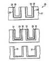
- FIGS. 5 a , 5 b and 5 cshow a further exemplary embodiment according to the invention of a component 26 .
- the figuresdescribe the introduction of a sacrificial layer during the silicide formation of a deep trench bottom electrode of the component 26 .
- trenches 28are etched into a preferably silicon-containing substrate 27 (a germanium-containing substrate may equally be used as well, and this equally applies with regard to the exemplary embodiments described above), said trenches subsequently being covered at the walls with a very thin intermediate layer 29 having a thickness of a few monolayers.
- the intermediate layer 29may be e.g. Ta 2 O 5 in this case.
- a metallic layer 30e.g. made of tungsten, is subsequently deposited on to the intermediate layer 29 .
- the intermediate layerprevents the reaction between the precursors used and the substrate 27 during the subsequent deposition of a metal layer.
- a simultaneous diffusion of the tungsten and of the siliconthen takes place through the intermediate layer 29 , which has the effect—see FIG. 5 a —that a WSi x layer 31 forms in a manner governed by diffusion on both sides of the intermediate layer 29 .
- the upper silicide layer 31may be etched away by selected etching, in which case the intermediate layer 29 may also additionally be concomitantly removed in this etching process, so that ultimately all that remains is the silicide layer 31 which, on the basis of FIG. 5 b , is situated below the intermediate layer 29 .
- the thickness of the metal layer forming the electrodeis significantly reduced and the diameter of the trench is increased again. The deposition of the node dielectric and also of the upper top electrode and further standard integration are subsequently effected.
- thermostable intermediate layerinstead of a thermostable intermediate layer, a thermally unstable layer which decomposes in the context of the silicide process and is broken up in this case and volatilizes through the previously applied metal layer.
- An etching process following the silicide formationfinally serves only for reducing the silicide layer.
- All silicon- or germanium-containing layers and also their oxides, nitrides or carbides and also metal silicides or metal silicates, which in each case likewise contain Si,may be used as the substrate to which the intermediate layer and finally the metal-containing and metallic layer are to be applied.
- Al 2 O 3 , Ta 2 O 5 , HfO 2 , TiO 2 or ZrO 2may be used in diverse stoichiometries as dielectrics that form the intermediate layer.
- All metals having a high melting point and also their nitrides and silicidessuch as W, Ti, Ta, Pd, Pt, V, Cr, Zr, Nb, Mo, Hf, Co, Ni, Rh, RhO, Ir and also other metals such as Al, Cu, Ag, Fe can be used as metals.
- the corresponding precursoris chosen depending on which metal or which metallic layer is to be applied.
- the respective dielectric that forms the intermediate layeris then also expediently to be chosen depending on this with regard to its diffusion-blocking and etching-resistant properties.
Landscapes
- Engineering & Computer Science (AREA)
- Condensed Matter Physics & Semiconductors (AREA)
- General Physics & Mathematics (AREA)
- Manufacturing & Machinery (AREA)
- Computer Hardware Design (AREA)
- Microelectronics & Electronic Packaging (AREA)
- Power Engineering (AREA)
- Physics & Mathematics (AREA)
- Chemical & Material Sciences (AREA)
- Chemical Kinetics & Catalysis (AREA)
- General Chemical & Material Sciences (AREA)
- Crystallography & Structural Chemistry (AREA)
- Materials Engineering (AREA)
- Mechanical Engineering (AREA)
- Metallurgy (AREA)
- Organic Chemistry (AREA)
- Electrodes Of Semiconductors (AREA)
- Internal Circuitry In Semiconductor Integrated Circuit Devices (AREA)
- Semiconductor Memories (AREA)
- Insulated Gate Type Field-Effect Transistor (AREA)
- Semiconductor Integrated Circuits (AREA)
Abstract
Description
Claims (9)
Applications Claiming Priority (3)
| Application Number | Priority Date | Filing Date | Title |
|---|---|---|---|
| DE10121132ADE10121132A1 (en) | 2001-04-30 | 2001-04-30 | Method for producing a metallic or metal-containing layer using a precursor on a silicon- or germanium-containing layer, in particular an electronic component |
| DE10121132.5 | 2001-04-30 | ||
| PCT/EP2002/004521WO2002088419A1 (en) | 2001-04-30 | 2002-04-24 | Method for production of a metallic or metal-containing layer |
Related Parent Applications (1)
| Application Number | Title | Priority Date | Filing Date |
|---|---|---|---|
| PCT/EP2002/004521ContinuationWO2002088419A1 (en) | 2001-04-30 | 2002-04-24 | Method for production of a metallic or metal-containing layer |
Publications (2)
| Publication Number | Publication Date |
|---|---|
| US20040132313A1 US20040132313A1 (en) | 2004-07-08 |
| US6960524B2true US6960524B2 (en) | 2005-11-01 |
Family
ID=7683250
Family Applications (1)
| Application Number | Title | Priority Date | Filing Date |
|---|---|---|---|
| US10/692,150Expired - Fee RelatedUS6960524B2 (en) | 2001-04-30 | 2003-10-21 | Method for production of a metallic or metal-containing layer |
Country Status (7)
| Country | Link |
|---|---|
| US (1) | US6960524B2 (en) |
| EP (1) | EP1383938B1 (en) |
| JP (1) | JP4056396B2 (en) |
| KR (1) | KR100583246B1 (en) |
| DE (2) | DE10121132A1 (en) |
| TW (1) | TWI306630B (en) |
| WO (1) | WO2002088419A1 (en) |
Families Citing this family (5)
| Publication number | Priority date | Publication date | Assignee | Title |
|---|---|---|---|---|
| DE10121132A1 (en) | 2001-04-30 | 2002-10-31 | Infineon Technologies Ag | Method for producing a metallic or metal-containing layer using a precursor on a silicon- or germanium-containing layer, in particular an electronic component |
| FR2859822B1 (en) | 2003-09-16 | 2006-05-05 | Commissariat Energie Atomique | INTERCONNECTION STRUCTURE WITH LOW DIELECTRIC CONSTANT |
| JP4216707B2 (en)* | 2003-12-25 | 2009-01-28 | 株式会社東芝 | Manufacturing method of semiconductor device |
| JP2012059958A (en)* | 2010-09-09 | 2012-03-22 | Rohm Co Ltd | Semiconductor device and method of manufacturing the same |
| CN111162039A (en)* | 2018-11-08 | 2020-05-15 | 长鑫存储技术有限公司 | Metal conductive structure and preparation method of semiconductor device |
Citations (10)
| Publication number | Priority date | Publication date | Assignee | Title |
|---|---|---|---|---|
| US5654233A (en) | 1996-04-08 | 1997-08-05 | Taiwan Semiconductor Manufacturing Company Ltd | Step coverage enhancement process for sub half micron contact/via |
| DE19820147A1 (en) | 1997-12-31 | 1999-07-01 | Samsung Electronics Co Ltd | Process for forming a conductive layer using an atomic layer deposition process |
| WO2000006795A1 (en) | 1998-07-27 | 2000-02-10 | Applied Materials, Inc. | Cvd tungsten deposition on oxide substrates |
| DE19853598A1 (en) | 1998-08-07 | 2000-02-10 | Samsung Electronics Co Ltd | Manufacture of thin film by atomic layer deposition |
| US6077774A (en)* | 1996-03-29 | 2000-06-20 | Texas Instruments Incorporated | Method of forming ultra-thin and conformal diffusion barriers encapsulating copper |
| US6139700A (en) | 1997-10-01 | 2000-10-31 | Samsung Electronics Co., Ltd. | Method of and apparatus for forming a metal interconnection in the contact hole of a semiconductor device |
| US6144060A (en) | 1997-07-31 | 2000-11-07 | Samsung Electronics Co., Ltd. | Integrated circuit devices having buffer layers therein which contain metal oxide stabilized by heat treatment under low temperature |
| US6203613B1 (en)* | 1999-10-19 | 2001-03-20 | International Business Machines Corporation | Atomic layer deposition with nitrate containing precursors |
| DE10121132A1 (en) | 2001-04-30 | 2002-10-31 | Infineon Technologies Ag | Method for producing a metallic or metal-containing layer using a precursor on a silicon- or germanium-containing layer, in particular an electronic component |
| US6800521B2 (en)* | 2000-08-30 | 2004-10-05 | Micron Technology, Inc. | Process for the formation of RuSixOy-containing barrier layers for high-k dielectrics |
- 2001
- 2001-04-30DEDE10121132Apatent/DE10121132A1/enactivePending
- 2002
- 2002-03-15TWTW091105004Apatent/TWI306630B/ennot_activeIP Right Cessation
- 2002-04-24DEDE50207441Tpatent/DE50207441D1/ennot_activeExpired - Lifetime
- 2002-04-24EPEP02730204Apatent/EP1383938B1/ennot_activeExpired - Lifetime
- 2002-04-24KRKR1020037014171Apatent/KR100583246B1/ennot_activeExpired - Fee Related
- 2002-04-24JPJP2002585696Apatent/JP4056396B2/ennot_activeExpired - Fee Related
- 2002-04-24WOPCT/EP2002/004521patent/WO2002088419A1/enactiveIP Right Grant
- 2003
- 2003-10-21USUS10/692,150patent/US6960524B2/ennot_activeExpired - Fee Related
Patent Citations (10)
| Publication number | Priority date | Publication date | Assignee | Title |
|---|---|---|---|---|
| US6077774A (en)* | 1996-03-29 | 2000-06-20 | Texas Instruments Incorporated | Method of forming ultra-thin and conformal diffusion barriers encapsulating copper |
| US5654233A (en) | 1996-04-08 | 1997-08-05 | Taiwan Semiconductor Manufacturing Company Ltd | Step coverage enhancement process for sub half micron contact/via |
| US6144060A (en) | 1997-07-31 | 2000-11-07 | Samsung Electronics Co., Ltd. | Integrated circuit devices having buffer layers therein which contain metal oxide stabilized by heat treatment under low temperature |
| US6139700A (en) | 1997-10-01 | 2000-10-31 | Samsung Electronics Co., Ltd. | Method of and apparatus for forming a metal interconnection in the contact hole of a semiconductor device |
| DE19820147A1 (en) | 1997-12-31 | 1999-07-01 | Samsung Electronics Co Ltd | Process for forming a conductive layer using an atomic layer deposition process |
| WO2000006795A1 (en) | 1998-07-27 | 2000-02-10 | Applied Materials, Inc. | Cvd tungsten deposition on oxide substrates |
| DE19853598A1 (en) | 1998-08-07 | 2000-02-10 | Samsung Electronics Co Ltd | Manufacture of thin film by atomic layer deposition |
| US6203613B1 (en)* | 1999-10-19 | 2001-03-20 | International Business Machines Corporation | Atomic layer deposition with nitrate containing precursors |
| US6800521B2 (en)* | 2000-08-30 | 2004-10-05 | Micron Technology, Inc. | Process for the formation of RuSixOy-containing barrier layers for high-k dielectrics |
| DE10121132A1 (en) | 2001-04-30 | 2002-10-31 | Infineon Technologies Ag | Method for producing a metallic or metal-containing layer using a precursor on a silicon- or germanium-containing layer, in particular an electronic component |
Also Published As
| Publication number | Publication date |
|---|---|
| JP2004530299A (en) | 2004-09-30 |
| EP1383938A1 (en) | 2004-01-28 |
| JP4056396B2 (en) | 2008-03-05 |
| WO2002088419A1 (en) | 2002-11-07 |
| KR20040015209A (en) | 2004-02-18 |
| TWI306630B (en) | 2009-02-21 |
| DE50207441D1 (en) | 2006-08-17 |
| EP1383938B1 (en) | 2006-07-05 |
| DE10121132A1 (en) | 2002-10-31 |
| US20040132313A1 (en) | 2004-07-08 |
| KR100583246B1 (en) | 2006-05-24 |
Similar Documents
| Publication | Publication Date | Title |
|---|---|---|
| US6787468B2 (en) | Method of fabricating metal lines in a semiconductor device | |
| EP1020901B1 (en) | Method for making an integrated circuit capacitor including tantalum pentoxide | |
| US20210384035A1 (en) | Fluorine-Free Tungsten ALD And Tungsten Selective CVD For Dielectrics | |
| US6100188A (en) | Stable and low resistance metal/barrier/silicon stack structure and related process for manufacturing | |
| US6583021B2 (en) | Method of fabricating capacitor having hafnium oxide | |
| US6207561B1 (en) | Selective oxidation methods for metal oxide deposition on metals in capacitor fabrication | |
| KR100471407B1 (en) | Method for fabricating transistor with polymetal gate electrode | |
| US6960524B2 (en) | Method for production of a metallic or metal-containing layer | |
| US5970309A (en) | Method of manufacturing a capacitor and a capacitor electrode in semiconductor device | |
| US6706607B2 (en) | Method for fabricating capacitor in semiconductor device | |
| US6908806B2 (en) | Gate metal recess for oxidation protection and parasitic capacitance reduction | |
| US20020197859A1 (en) | Method for forming a polycide structure in a semiconductor device | |
| JP4347479B2 (en) | Field effect transistor | |
| KR100681211B1 (en) | Gate electrode having a double diffusion barrier and method of manufacturing a semiconductor device having the same | |
| US6979657B2 (en) | Method for forming a dielectric layer in a semiconductor device | |
| US20070072418A1 (en) | Method of forming tungsten silicide layer and method of fabricating semiconductor element using same | |
| US20020098682A1 (en) | Semiconductor device fabrication method | |
| JPH11204757A (en) | Method for manufacturing semiconductor device | |
| TWI329340B (en) | Method for manufacturing semiconductor device | |
| KR100454256B1 (en) | Method for fabricating capacitor having ruthenium bottom-electrode | |
| US20040147102A1 (en) | Production method for a semiconductor component | |
| KR20030049141A (en) | A forming method of titanium nitride layer and fabricating method of semiconductor device | |
| US6190991B1 (en) | Method for fabricating a capacitor | |
| KR100673203B1 (en) | Capacitor Manufacturing Method of Semiconductor Device | |
| KR100729905B1 (en) | Capacitor Manufacturing Method of Semiconductor Device |
Legal Events
| Date | Code | Title | Description |
|---|---|---|---|
| AS | Assignment | Owner name:INFINEON TECHNOLOGEIS AG, GERMANY Free format text:ASSIGNMENT OF ASSIGNORS INTEREST;ASSIGNORS:HECHT, THOMAS;SELL, BERNHARD;SAENGER, ANNETTE;REEL/FRAME:014175/0993;SIGNING DATES FROM 20031104 TO 20031105 | |
| FEPP | Fee payment procedure | Free format text:PAYOR NUMBER ASSIGNED (ORIGINAL EVENT CODE: ASPN); ENTITY STATUS OF PATENT OWNER: LARGE ENTITY | |
| FPAY | Fee payment | Year of fee payment:4 | |
| AS | Assignment | Owner name:QIMONDA AG,GERMANY Free format text:ASSIGNMENT OF ASSIGNORS INTEREST;ASSIGNOR:INFINEON TECHNOLOGIES AG;REEL/FRAME:023768/0001 Effective date:20060425 Owner name:QIMONDA AG, GERMANY Free format text:ASSIGNMENT OF ASSIGNORS INTEREST;ASSIGNOR:INFINEON TECHNOLOGIES AG;REEL/FRAME:023768/0001 Effective date:20060425 | |
| FPAY | Fee payment | Year of fee payment:8 | |
| AS | Assignment | Owner name:INFINEON TECHNOLOGIES AG, GERMANY Free format text:ASSIGNMENT OF ASSIGNORS INTEREST;ASSIGNOR:QIMONDA AG;REEL/FRAME:035623/0001 Effective date:20141009 | |
| AS | Assignment | Owner name:POLARIS INNOVATIONS LIMITED, IRELAND Free format text:ASSIGNMENT OF ASSIGNORS INTEREST;ASSIGNOR:INFINEON TECHNOLOGIES AG;REEL/FRAME:036723/0021 Effective date:20150708 | |
| REMI | Maintenance fee reminder mailed | ||
| LAPS | Lapse for failure to pay maintenance fees | Free format text:PATENT EXPIRED FOR FAILURE TO PAY MAINTENANCE FEES (ORIGINAL EVENT CODE: EXP.) | |
| STCH | Information on status: patent discontinuation | Free format text:PATENT EXPIRED DUE TO NONPAYMENT OF MAINTENANCE FEES UNDER 37 CFR 1.362 | |
| FP | Lapsed due to failure to pay maintenance fee | Effective date:20171101 |