US6957608B1 - Contact print methods - Google Patents
Contact print methodsDownload PDFInfo
- Publication number
- US6957608B1 US6957608B1US10/288,357US28835702AUS6957608B1US 6957608 B1US6957608 B1US 6957608B1US 28835702 AUS28835702 AUS 28835702AUS 6957608 B1US6957608 B1US 6957608B1
- Authority
- US
- United States
- Prior art keywords
- stamp
- nanoparticles
- liquid
- protruding
- features
- Prior art date
- Legal status (The legal status is an assumption and is not a legal conclusion. Google has not performed a legal analysis and makes no representation as to the accuracy of the status listed.)
- Expired - Fee Related, expires
Links
Images


Classifications
- H—ELECTRICITY
- H10—SEMICONDUCTOR DEVICES; ELECTRIC SOLID-STATE DEVICES NOT OTHERWISE PROVIDED FOR
- H10K—ORGANIC ELECTRIC SOLID-STATE DEVICES
- H10K71/00—Manufacture or treatment specially adapted for the organic devices covered by this subclass
- H10K71/60—Forming conductive regions or layers, e.g. electrodes
- H10K71/611—Forming conductive regions or layers, e.g. electrodes using printing deposition, e.g. ink jet printing
- H—ELECTRICITY
- H05—ELECTRIC TECHNIQUES NOT OTHERWISE PROVIDED FOR
- H05K—PRINTED CIRCUITS; CASINGS OR CONSTRUCTIONAL DETAILS OF ELECTRIC APPARATUS; MANUFACTURE OF ASSEMBLAGES OF ELECTRICAL COMPONENTS
- H05K3/00—Apparatus or processes for manufacturing printed circuits
- H05K3/10—Apparatus or processes for manufacturing printed circuits in which conductive material is applied to the insulating support in such a manner as to form the desired conductive pattern
- H05K3/12—Apparatus or processes for manufacturing printed circuits in which conductive material is applied to the insulating support in such a manner as to form the desired conductive pattern using thick film techniques, e.g. printing techniques to apply the conductive material or similar techniques for applying conductive paste or ink patterns
- H—ELECTRICITY
- H10—SEMICONDUCTOR DEVICES; ELECTRIC SOLID-STATE DEVICES NOT OTHERWISE PROVIDED FOR
- H10K—ORGANIC ELECTRIC SOLID-STATE DEVICES
- H10K71/00—Manufacture or treatment specially adapted for the organic devices covered by this subclass
- H10K71/621—Providing a shape to conductive layers, e.g. patterning or selective deposition
Definitions
- This inventionrelates to the field of contact printing for the fabrication of micro-devices. More particularly, this invention relates to systems, devices for and methods of controlling print quality using liquid embossing techniques for the fabrication of micro-devices.
- Micro-mechanical, micro-electrical, and micro-optical devicesare most typically fabricated using mask and etching steps to define each patterned layer within the device. These steps are labor intensive, expensive and typically require specialized processing equipment specifically tailored for a single fabrication process.
- One of the goals for nano-technologyis the development of techniques and materials that enable the fabrication of micro-electronic devices on a variety of substrates using contact printing methods which allows for the direct replication of patterned device layers.
- Contact printing methodsoffer a reduction in the number of steps required to fabricate micro-devices as well as provide for the development of diversified processing methods for printing a wide range of patterned device layers on a wide range of substrate surfaces cheaply and with high throughput.
- the present inventionis directed to methods of and systems for controlled printing using liquid embossing techniques.
- the method and system of the present inventionis particularly useful for fabricating patterned device layers for micro-electronic, micro-optical or micro-mechanical devices (viz. micro-devices).
- liquid embossingis used to fabricate thin film transistors (TFTs), and other electronic devices, alone or in combination with physical deposition processes.
- TFTsthin film transistors
- Methods and materials for the fabrication of micro-electronic devices using liquid embossing techniques in combination with physical deposition techniquesare further described in the U.S. patent application Ser. No. 10/251,077, filed Sep. 20, 2002, and entitled. “FABRICATION OF MICRO-ELECTRONIC DEVICES”, the contents of which are hereby incorporated by reference.
- Liquid embossinginvolves depositing or coating a layer of liquid ink onto a suitable substrate or print medium.
- Suitable substrates and print mediainclude silicon, quartz, glass, metal, sapphire and polymer substrates.
- Liquid embossingis also used to print device layers over any number of previously formed device layers or partial device structures.
- the layer of liquid inkis deposited, or coated, onto the substrate or the print medium using any suitable technique including, but not limited to, spin-coating, ink-jet coating, extrusion coating and dip coating.
- the preferred technique for depositing, or coating, the layer of liquid ink onto the substrate or the print mediumdepends on the properties of both the substrate or print medium and the liquid ink.
- Liquid inksin accordance with the embodiments of the invention, comprise nanoparticles that are dispersed in a solvent medium.
- the solvent mediumpreferably comprises an organic solvent having five or more carbon atoms.
- Suitable organic solventsinclude, but are not limited to, tetralin, cyclohexylbenzene, terpineols, 2-ethylhexanol, 3-octanol, indan, dimethylbenzene, gamma-butyrolactone, cyclohexanone, dihydrobenzofuran, decaline, 1-heptanol, 2-methyl-2,4-pentanediol, phenetylalcohol, citronellol, geraniol, diethyleneglycolmonoethylether, diethyleneglycolmonomethylether, phenetole, ethyllactate, diethylphthalate, glyme, diglyme, triglyme
- Nanoparticles used in liquid ink formulationsare metal nanoparticles, semiconductor nanoparticles, dielectric nanoparticles, magnetic nanoparticles, piezo-electric nanoparticles, pyro-electric nanoparticles, oxide nanoparticles or combinations thereof and, preferably, have sizes in a range of 1.0-100 nanometers.
- the nanoparticlesare metal nanoparticles
- the nanoparticlespreferably comprise a metal selected from Ag, Pd, Rh, Cu, Pt, Ni, Fe, Ru, Os, Mn, Sn, Cr, Mo, W, Co, Ir, Zn, Au, Cd and a combination thereof.
- a liquid inkcomprises a polymer, or a polymer precursor, such as a photo-resist polymer and/or a spin-on-glass polymer.
- Nanoparticles, in accordance with further embodiments of the inventionare dispensed in a solvent and combined with a polymer precursor for depositing metallic-polymer thin films.
- a stamp with a patterned region comprising protruding featuresis brought into contact with a layer of the liquid ink, such that the protruding features displace the liquid link from or across the substrate surface to form a patterned layer.
- the patterned layeris then cured to form a solid patterned device layer.
- an adhesion promoter or interface layercan be formed prior to depositing or coating the liquid ink.
- Adhesion promoters and/or interface layersare further described in U.S. patent application Ser. No. 10/226,903, filed Aug. 22, 2002, entitled “INTERFACE LAYER FOR THE FABRICATION OF ELECTROIC DEVICES”, the contents of which are hereby incorporated by reference.
- Stamps suitable for liquid embossingcan be formed from any number or materials or combinations of materials, but preferably comprise an elastomeric material, such as polydimethylsiloxane (PDMS).
- PDMSpolydimethylsiloxane
- the surface energies between the protruding features of the stamp and the liquid inkare sufficiently mismatched, and the surface energies between the substrate surface, or print medium surface, and the liquid ink are sufficiently mismatched, such that the liquid ink is readily displaced from the surface of the substrate by the protruding features of the stamp when the stamp is brought into contact with the layer of liquid ink.
- the ability of the protruding features to displace liquid inkis also affected by the geometry of the protruding features, as explained in detail below.
- the rate with which one or more liquid ink solvents are absorbed by the stampis the rate with which one or more liquid ink solvents are absorbed by the stamp.
- the stampor at least a portion of the stamp, absorbs one or more of the ink solvents in order to “set” or “partially cure” the printed liquid layer during the embossing process before the stamp is removed from contact with the printed liquid layer.
- Solvent absorption by the stamp to set the printed liquid layer during the embossing processis believed to be an important means for preventing the patterned layer from re-flowing into regions of the substrate surface where the liquid ink has been displaced by the protruding features.
- the method and the system of the present inventionpreferably utilize a stamp structure with differentiated protruding surfaces and recessed surfaces to enhance the printing capabilities of the stamp.
- a stampis modified to render the protruding surfaces substantially different from the recessed surfaces.
- the stampin accordance with the present invention, is modified by treating the protruding features, the recessed features or a combination thereof, with a surface modifier (such as a metal, a polymer and/or a fluorochemical), chemical exposure (such as with an oxidant or an etchant), radiation (such as heat or light) and/or any combination thereof.
- a surface modifiersuch as a metal, a polymer and/or a fluorochemical
- chemical exposuresuch as with an oxidant or an etchant
- radiationsuch as heat or light
- a thin layer of the surface modifiercan be deposited onto regions of contact between the substrate or print medium and the stamp during the embossing process which alters or modifies the surface properties of the substrate or print medium in the regions of contact and prevents the re-flow of the liquid ink.
- treating the stampin accordance with the present invention, enhances the ability of the protruding features to displace the liquid ink by modifying the surface energy and/or modifying the wettability of the protruding stamp surfaces relative to the recessed stamp surfaces.
- a protective maskis provided over the protruding surfaces or over the recessed surfaces of the stamp while the other of the protruding surfaces or recessed surfaces are being treated or modified.
- the rate of solvent absorption by the stampis controlled to optimize the soft curing of patterned liquid layers during the embossing process.
- the rate of solvent absorption by the stampis controlled by pre-treating a portion of the stamp with a solvent prior to embossing, drawing a vacuum on the stamp while embossing, heating the substrate structure, the stamp and/or the liquid ink while embossing, judicious choice of ink solvent(s) and stamp materials, or any combination thereof.
- a stamp with differentiated surfacesis formed by making the protruding features of the stamp from a first material and the recessed features of the stamp from a second material.
- the protruding features of the stampare formed from a first material which is a relatively non-porous material, such as polydimethylsiloxane (PDMS) and the recessed features, or a portion thereof, are formed from a second material which is relatively porous.
- the protruding features of the stampare cast from a mold using a relatively non-porous curable elastomeric material and are attached to a suitable porous backing.
- Suitable porous backingscomprise metal, glass, glass fiber, quartz, polymer foam, mixed cellulose, polycarbonate, polyimide, polytetrafluoroethylene (PTFE), nylon, polyether sulfone (PES), polypropylene, mixed cellulose, polyvinylidene fluoride (PVDF), polysiloxane (such as PDMS) and/or combinations thereof.
- a stampis treated or conditioned between prints.
- the stampis dipped into a solvent bath between prints and/or is cleaned by contact with an adhesive surface to remove residue between prints.
- a stampis fabricated with contoured features.
- a masteris formed with contoured cavities for casting a stamp with contoured features.
- a stampis conditioned or reconditioned between prints to remove solvent or solvents, as explained in detail below.
- FIGS. 1A-Dshow the steps of making an elastomeric stamp, in accordance with the embodiments of the invention.
- FIGS. 2A-Dshow the steps of making a stamp with protruding features formed from a first material and recessed features formed from a second material, in accordance with the embodiments of the invention.
- FIGS. 3A-Fshow the steps of making a stamp with differentiated protruding surfaces and recessed surfaces, in accordance with the embodiments of the invention.
- FIGS. 4A-Eshow the use of a protective mask formed over the recessed stamp surfaces prior to treating the protruding stamp surfaces, in accordance with the method of the invention.
- FIGS. 5A-Cshow the use of a protective mask formed over the protruding stamp surfaces prior to treating the recessed stamp surfaces, in accordance with the method of the invention.
- FIGS. 6A-Bshow pre-treatment of a stamp, in accordance with the embodiments of the invention.
- FIGS. 7A-Eshow cross-sectional views of protruding stamp features or recessed features with contoured surfaces.
- FIGS. 8A-Eshow cross-sectional views of master structures with contoured cavities for casting stamps with contoured protruding features, such as illustrated in FIGS. 7A-E .
- FIG. 9shows a liquid embossing system, in accordance with the embodiments of the invention.
- a micro-deviceis fabricated by forming a plurality of patterned device layers, wherein one or more of the patterned device layers are formed using liquid embossing with a stamp.
- the printing processis controlled by using a stamp with differentiated protruding surfaces and recessed surfaces, by controlling the printing conditions and/or a combination thereof.
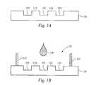
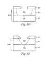
- FIGS. 1A-Dillustrate exemplary steps for making an elastomeric stamp structure 128 (FIG. 1 D).
- a master 100is formed having a series of recessed features 105 and protruding features 110 , which provides a negative impression for casting the stamp structure 128 .
- the actual dimensions of the features 105 and 110depend on the intended application of the stamp structure 128 and are determined by the method used to pattern the master 100 . In general, however, feature sizes as small as 150 nanometers are possible using lithography techniques.
- the master structure 100is formed from any number of suitable materials including, but not limited to, silicon-based materials (such as silicon, silicon dioxide, and silicon nitride) and metal.
- silicon-based materialssuch as silicon, silicon dioxide, and silicon nitride
- metalsuch as silicon, silicon dioxide, and silicon nitride
- Methods and materials used for making master structures suitable for casting elastomeric stampsare further described in U.S. patent application Ser. No. 09/525,734, entitled “Fabrication of Finely Features Devices by Liquid Embossing” and in U.S. patent application Ser. No. 09/519,722, entitled “Method for Manufacturing Electronic and Electro Mechanical Elements and Devices by Thin Film Deposition and Imaging”, referenced previously.
- an uncured liquid elastomer 120such as polydimethylsiloxane, is poured or deposited over the master structure 100 , such that the liquid elastomer 120 fills the recessed features 105 and covers the protruding features 110 .
- a containment structure or wall 115is provided to form a well 125 .
- the well 125helps to hold the liquid elastomer 120 over the master structure 100 and helps to control the thickness of the stamp structure 128 formed.
- the elastomer 120is then cured to form the stamp structure 128 .
- the method and the conditions required to cure the liquid elastomer 120vary depending on the type of elastomer used. In the case of PDMS, the liquid elastomer 120 is curable by heating the liquid elastomer 120 in an oven at approximately 80 degrees Celsius for approximately 2 hours. Other liquid elastomers are curable using radiation, such as ultra violet radiation and/or chemically by, for example, adding a crossing linking agent to the liquid elastomer 120 .
- the stamp structure 128is removed or separated from the master structure 100 and the protruding stamp surfaces 131 and recessed stamp surfaces 133 can then be used to emboss a suitable liquid ink and facilitate the direct patterning of electrical, biological, chemical and/or mechanical materials.
- the stamp 128also preferably facilitates the curing of patterned layers by absorbing solvent from the ink, referred to herein as soft curing of a patterned liquid layer. Soft curing of patterned liquid layers by the stamp 128 helps to form a stable pattern with a high degree of feature definition.
- stamp materials, designs, ink materials and ink formulationscan be judiciously selected to control the rate of solvent absorption.
- a stamp structureis formed form multiple materials, such that the stamp structure has differentiated protruding surfaces and recessed surfaces, wherein the recessed surfaces are formed from a porous material, or an absorbent material, in order to remove solvent more rapidly from the ink while embossing a liquid layer.
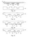
- FIGS. 2A-Dillustrate the steps of making a stamp with differentiated protruding surfaces and recessed surfaces, in accordance with the embodiments of the invention.
- a first material 220is poured or coated onto a master structure 200 comprising recessed features 205 and protruding features 210 .
- the first material 220is poured over the master 200 and at least fills the recessed features 205 , as shown in FIG. 2 B.
- the first material 220is preferably a curable liquid elastomer, such as PDMS, which forms the partial stamp structure 226 ( FIG. 2D ) and provides protruding stamp surfaces 230 .
- a second material 225is attached to the first material or the partial stamp structure 226 .
- the second material 225in accordance with the invention is a curable elastomer, which when cured, forms a backing structure 225 comprising the recessed surfaces 240 (FIG. 2 D), wherein the recessed surfaces 240 have different absorption properties, wetting properties, surface energy properties, or a combination thereof relative to the protruding surfaces 230 of the partial stamp structure 226 .
- the first material 220 and second material 225are curable elastomers, they can be cured separately or together.
- the backing structure 225is a preformed solid, which is brought into contact with the first material 220 .
- the first material 220is a curable elastomer
- curing the first material 220 with the backing structure 225 in contact with the first material 220is sufficient to attach the backing structure 225 to the partial stamp structure 226 formed.
- the backing material 225is a porous material that is capable of absorbing organic solvents.
- Suitable backing materialsinclude, but are not limited to, metal, glass, glass fiber, quartz, polymer foam, mixed cellulose, polycarbonate, polyimide, polytetrafluoroethylene (PTFE), nylon, polyether sulfone (PES), polypropylene, mixed cellulose polyvinylidene fluoride (PVDF), polysiloxane (such as PDMS) and combinations thereof.
- the partial stamp structure 226can be coupled or attached to make a stamp 235 with differentiated protruding surfaces 230 and recessed surfaces 240 using any number of methods including providing a third material (not shown), such as an adhesive material between partial stamp structure 226 and the backing structure 225 .
- the resultant stamp structure 235is then removed or separated from the master 200 and the protruding surfaces 230 comprising the first materials 220 and the recessed surfaces 240 comprising the second materials 225 can be used to emboss a suitable liquid ink in a liquid embossing process, such as described above.
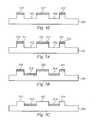
- a stamp 300is formed from one or more materials, as described above.
- the stamp 300comprises a set of protruding surfaces 311 , 313 , 315 and 317 and a set of recessed surfaces 312 , 314 and 316 for embossing a pattern into a layer of liquid ink.
- the set of protruding surfaces 311 , 313 , 315 and 317is treated to form a modified stamp 300 ′ with differentiated sets of protruding surfaces 311 ′, 313 ′, 315 ′ and 317 ′ and recessed surfaces 312 , 314 , and 316 , as shown in FIG. 3 B.
- the set of recessed surfaces 312 , 314 , and 316is selectively modified to form a modified stamp 300 ′′ with a differentiated set of protruding surfaces 311 , 313 , 315 and 317 and recessed surfaces 312 ′, 314 ′, and 316 ′, as shown in FIG. 3 C.
- the set of protruding surfaces 311 , 313 , 315 and 317 and the set of recessed surfaces 312 , 314 and 316are both selectively treated to form a modified stamp (not shown) with a differentiated set of protruding surfaces 311 ′, 313 ′, 315 ′ and 317 ′ and set of recessed surfaces 312 ′, 314 ′ and 316 ′.
- FIGS. 3D-Fwill now be used to illustrate a technique for selectively treating a set of protruding surfaces, in accordance with an embodiment of the present invention.
- a surface modifier 326is coated or deposited onto a substrate 325 .
- the surface modifier 326is a solvent, an acid, an oxidant, a polymer, a pre-polymer, a fluorochemical (such as a fluorocarbon, a fluorosilicon or other fluorinated compound), or any other material and/or combination of materials which is capable of modifying the absorption properties, the wetting properties and/or the surface energy properties of the set of the protruding stamp surfaces 311 , 313 , 315 and 317 .
- a fluorochemicalsuch as a fluorocarbon, a fluorosilicon or other fluorinated compound
- the stamp 300is brought into contact with the surface modifier 326 , as shown FIG. 3E , such that at least a portion of the protruding surfaces 311 , 313 , 315 and 317 are coated with the surface modifier 326 .
- the surface modifier 326either adheres to or is absorbed into the protruding surfaces 311 , 313 , 315 and 317 and chemically and/or physically alters the protruding surfaces 311 ′, 313 ′, 315 ′ and 317 ′ to form the modified stamp structure 300 ′.
- the modified stamp structure 300 ′can then be used to emboss a layer of liquid ink.
- a stampin accordance with further embodiments of the invention, is modified to have differentiated protruding surfaces and recessed surfaces by coating or treating selected portions of a stamp using any number of methods including vapor coating and sputter coating methods.
- a modified stamp structure with differentiated protruding surfaces and recessed surfacesis formed by selectively exposing one or both of the protruding surfaces and recessed surfaces to a radiation source, such as a heat source, light source, or electron beam source, wherein the exposed surfaces are modified by the radiation source.
- a stampin accordance with yet further embodiments of the invention is formed by blanket coating an embossing surface of a stamp comprising protruding and recessed surfaces with a surface modifier and then selectively removing the surface modifier from a portion of the protruding surfaces and/or recessed surfaces to form differentiated embossing surfaces.
- a maskis preferably provided to prevent selected surfaces from becoming coated or contaminated by the surface modifier.
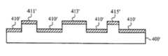
- a stamp 400comprises protruding surfaces 411 , 413 and 415 and recessed surfaces 412 and 414 , as described previously.
- a modified stamp 400 ′FIGS. 4D-E
- the compliment of protruding surfaces 411 , 413 and 415 and recessed surfaces 412 and 414are coated with a masking material 410 as shown in Figured 4 B.
- the masking material 410is any masking material which can be selectively removed, but is preferably a photo-resist that can be exposed and developed using lithographic techniques in the art.
- the masking material 410is selectively removed from the protruding surfaces 411 , 413 , and 415 of the stamp 400 to form the mask 410 ′, as shown in FIG. 4 C.
- the protruding surfaces 411 , 413 and 415 of the stamp 400are then selectively treated with a surface modifier to form the modified stamp 400 ′ with differentiated embossing surfaces 410 ′, 411 ′, 413 ′ and 415 ′.
- the mask 410 ′can be removed to form a modified stamp 400 ′ with differentiated embossing surfaces 411 ′, 412 , 413 ′, 414 and 415 ′.
- a stamp 500comprising protruding surfaces 511 , 513 and 515 and recessed surfaces 512 and 514 is provided with a mask 525 .
- the mask 525is selectively formed on the protruding surfaces 511 , 513 and 515 , by dip-coating the protruding surfaces 511 , 513 and 515 into a curable masking material (FIG. 3 E), or any other method suitable for coating or depositing a masking material onto the protruding surfaces 511 , 513 and 515 .
- the recessed surfacesare then selectively treated with a surface modifier to form a modified stamp structure 500 ′ with differentiated embossing surfaces 525 , 512 ′ and 514 ′, as shown in FIG. 5 B.
- the mask 525is removed to form the modified stamp 500 ′ with a differentiated embossing surfaces 511 , 512 ′ 513 , 514 ′ and 515 .
- a stamp 600comprising an embossing surface 605 comprising protruding and recessed surfaces, as described above, is non-selectively treated in order to convert the stamp 600 to a modified stamp 601 (FIG. 6 B).
- Non-selective treatment methodsinclude, but are not limited to thermal treatment of the stamp 600 , soaking or pre-soaking the stamp 600 in a solvent or other material which is absorbed into the stamp 600 , photo-treatment or radiation treatment of the stamp 600 , pressure treatment of the stamp 600 and combinations thereof.
- Non-selective treatment of the stamp 600 to form the modified stamp 601can also be used in combination with the selective surface modification techniques described in detail above.
- stamp structuresthus far have been illustrated with protruding features and recessed features having substantially flat surfaces.
- stamps with contoured protruding and/or recessed featuresare preferred, because the contoured protruding and/or recessed features can facilitate the displacement of liquid during an embossing process.
- FIGS. 7A-Eillustrate a few exemplary geometries of contoured protruding and/or recessed embossing stamp features, in accordance with the embodiments of the invention.
- FIG. 7Ashows a cross-sectional view of a rounded contoured stamp feature
- Figure Bshows a cross-sectional view of an oval contoured stamp feature
- FIG. 7Cshows a cross-sectional view of a triangular contoured stamp feature
- FIG. 7Dshows a cross-sectional view of a trapezoidal stamp feature
- FIG. 7Eshows a cross-sectional view of a stamp feature with rounded corners. It will be clear to one skilled in the art that any number of different geometries and combinations of geometries for protruding stamp features and recessed stamp features are within the scope of the invention.
- FIGS. 8A-Eshow several master structures with contoured cavity profiles to cast stamps with contoured features, such as described above.
- FIG. 8Ashows a structure with an etch mask 803 formed over a suitable substrate 801 that is isotropically etched to form the curved or rounded cavity 805 ;
- FIG. 5Bshows a structure with a mask 813 formed over the a suitable substrate 811 that is anisotropically etched through the mask 813 to form an oval shaped cavity 815 ; and
- FIGS. 8Cshows a structure with a mask 823 formed over a suitable substrate 821 that is isotropically etched through the mask 823 to form a triangular cavity 825 .
- FIGS. 8A-Cshow profiles of contoured cavities that are formed without providing etch-stop layers. By providing etch-stop layers, contoured cavities can be formed which have flattened bottom profiles, such as shown in FIGS. 8D-E .
- a master structure with a curved cavity 835 and a flattened bottom 836is formed by providing a substrate structure 830 with an etch-stop layer 832 , a sacrificial layer 831 and a mask 833 deposited over the sacrificial layer 831 .
- the sacrificial layer 831is isotropically etched through the mask 833 down to the etch-stop layer 832 to form the curved cavity 835 with the flattened bottom 836 .
- a master structure with a tapered cavity 845 and a flattened bottom 846is formed by providing a substrate structure 840 with an etch-stop layer 842 , a sacrificial layer 841 and a mask 843 deposited over the sacrificial layer 841 .
- the sacrificial layer 841is anisotropically or isotropically etched through the mask 843 down to the etch-stop layer 842 to form the tapered cavity 845 with the flattened bottom 846 .
- a system 950in accordance with the embodiments of the present invention comprises a mechanism for coupling a print medium 930 with stamp 925 .
- the stamp 925comprises an embossing surface 926 with protruding surfaces and recessed surfaces for embossing a print into a layer of liquid ink deposited on a print medium 930 , referred to herein as an inked print medium 931 .
- the system 950in accordance with the embodiments of the invention, comprises a drum structure 929 for holding the stamp 925 and for rolling the embossing surface 926 of the stamp 925 over the inked print medium 931 to emboss the features 951 , 953 , 955 and 957 through the layer of liquid ink to generate an embossed print medium 931 ′.
- All or a portion of the embossing surface 925 of the stamp 925comprises differentiated protruding surfaces and/or recessed surfaces that are modified by the methods described above.
- the system 950is configured to move the inked print medium 931 in a direction D, along the stamp 925 , such that the inked print medium 931 passes under a stationary, moving and/or rotating drum structure 929 .
- the system 950also preferably comprises an ink supply 901 for coating the print medium 930 with a suitable ink to form ink printed medium 931 .
- Suitable inksinclude, but are not limited to, nanoparticle inks, such as those described above.
- the system 950in accordance with yet further embodiments of the invention is configured to assist in the removal of solvent from the ink while embossing the inked print medium 931 by heating the stamp 925 and/or drawing a vacuum on the stamp 925 through the drum 929 .
- the system 925in yet further embodiments of the invention comprises a heat source 963 for heating the print medium 931 and/or ink, prior to, during or after embossing the inked print medium 931 .
- the system 925can be configured with rollers 960 and 961 for controlling the direction, movement and tension of the print medium 930 .
- the system 950can also be configured with an accumulator 970 and/or winder for controlling windup of the printed medium 931 ′.
- the system 950can further include alignment features for aligning the stamp 925 with the inked print medium 931 , drying and/or curing means 961 for exposing the printed medium 931 ′ to a curing radiation 960 and/or converting stations (not shown) for cutting and organizing the printed medium 931 ′.
Landscapes
- Engineering & Computer Science (AREA)
- Manufacturing & Machinery (AREA)
- Shaping Of Tube Ends By Bending Or Straightening (AREA)
Abstract
Description
This Patent Application claims priority under 35 U.S.C. 119(e) of the co-pending U.S. Provisional Patent Application Ser. No. 60/400,795, filed Aug. 2, 2002, and entitled “CONTROLLED PRINT METHODS”. The Provisional Patent Application, Ser. No. 60/400,795, filed Aug. 2, 2002, and entitled “CONTROLLED PRINT METHODS” is also hereby incorporated by reference.
This invention relates to the field of contact printing for the fabrication of micro-devices. More particularly, this invention relates to systems, devices for and methods of controlling print quality using liquid embossing techniques for the fabrication of micro-devices.
Micro-mechanical, micro-electrical, and micro-optical devices are most typically fabricated using mask and etching steps to define each patterned layer within the device. These steps are labor intensive, expensive and typically require specialized processing equipment specifically tailored for a single fabrication process.
One of the goals for nano-technology is the development of techniques and materials that enable the fabrication of micro-electronic devices on a variety of substrates using contact printing methods which allows for the direct replication of patterned device layers. Contact printing methods offer a reduction in the number of steps required to fabricate micro-devices as well as provide for the development of diversified processing methods for printing a wide range of patterned device layers on a wide range of substrate surfaces cheaply and with high throughput.
There are a number of challenges to developing methods of contact printing for the fabrication of micro-devices, including but not limited to developing inks that are suitable for patterning by contact print methods and developing systems suitable for producing multiple prints with high throughput. Accordingly, there is a continued need for new methods of and systems for fabricating patterned device layers using contact print methods.
The present invention is directed to methods of and systems for controlled printing using liquid embossing techniques. The method and system of the present invention is particularly useful for fabricating patterned device layers for micro-electronic, micro-optical or micro-mechanical devices (viz. micro-devices). For example, liquid embossing is used to fabricate thin film transistors (TFTs), and other electronic devices, alone or in combination with physical deposition processes. Methods and materials for the fabrication of micro-electronic devices using liquid embossing techniques in combination with physical deposition techniques are further described in the U.S. patent application Ser. No. 10/251,077, filed Sep. 20, 2002, and entitled. “FABRICATION OF MICRO-ELECTRONIC DEVICES”, the contents of which are hereby incorporated by reference.
Liquid embossing involves depositing or coating a layer of liquid ink onto a suitable substrate or print medium. Suitable substrates and print media include silicon, quartz, glass, metal, sapphire and polymer substrates. Liquid embossing is also used to print device layers over any number of previously formed device layers or partial device structures. The layer of liquid ink is deposited, or coated, onto the substrate or the print medium using any suitable technique including, but not limited to, spin-coating, ink-jet coating, extrusion coating and dip coating. The preferred technique for depositing, or coating, the layer of liquid ink onto the substrate or the print medium depends on the properties of both the substrate or print medium and the liquid ink.
Liquid inks, in accordance with the embodiments of the invention, comprise nanoparticles that are dispersed in a solvent medium. The solvent medium preferably comprises an organic solvent having five or more carbon atoms. Suitable organic solvents include, but are not limited to, tetralin, cyclohexylbenzene, terpineols, 2-ethylhexanol, 3-octanol, indan, dimethylbenzene, gamma-butyrolactone, cyclohexanone, dihydrobenzofuran, decaline, 1-heptanol, 2-methyl-2,4-pentanediol, phenetylalcohol, citronellol, geraniol, diethyleneglycolmonoethylether, diethyleneglycolmonomethylether, phenetole, ethyllactate, diethylphthalate, glyme, diglyme, triglyme, tetraglyme, pine oil, cineole, octanol, hexanol and pentanol.
Nanoparticles used in liquid ink formulations, in accordance with the embodiments of the invention, are metal nanoparticles, semiconductor nanoparticles, dielectric nanoparticles, magnetic nanoparticles, piezo-electric nanoparticles, pyro-electric nanoparticles, oxide nanoparticles or combinations thereof and, preferably, have sizes in a range of 1.0-100 nanometers. Where the nanoparticles are metal nanoparticles, the nanoparticles preferably comprise a metal selected from Ag, Pd, Rh, Cu, Pt, Ni, Fe, Ru, Os, Mn, Sn, Cr, Mo, W, Co, Ir, Zn, Au, Cd and a combination thereof. Nanoparticle inks and method for making the same are further described in the U.S. patent application Ser. No. 10/215,952, filed Aug. 9, 2002, and entitled “NANOPARTICLE SYNTHESES AND THE FORMATION OF INKS THEREFROM”, the contents of which are hereby incorporated by reference. In accordance with further embodiments of the present invention, a liquid ink comprises a polymer, or a polymer precursor, such as a photo-resist polymer and/or a spin-on-glass polymer. Nanoparticles, in accordance with further embodiments of the invention, are dispensed in a solvent and combined with a polymer precursor for depositing metallic-polymer thin films.
Regardless of the materials used to form a liquid ink, in order to emboss a layer of the liquid ink, a stamp with a patterned region comprising protruding features is brought into contact with a layer of the liquid ink, such that the protruding features displace the liquid link from or across the substrate surface to form a patterned layer. After the patterned layer is formed, the patterned layer is then cured to form a solid patterned device layer. In order to facilitate the adhesion of the patterned device layer to the substrate structure or print medium and/or to provide ohmic contact of the patterned device layer with a substrate and/or other device layer(s) therebelow, an adhesion promoter or interface layer can be formed prior to depositing or coating the liquid ink. Adhesion promoters and/or interface layers are further described in U.S. patent application Ser. No. 10/226,903, filed Aug. 22, 2002, entitled “INTERFACE LAYER FOR THE FABRICATION OF ELECTROIC DEVICES”, the contents of which are hereby incorporated by reference.
Stamps suitable for liquid embossing can be formed from any number or materials or combinations of materials, but preferably comprise an elastomeric material, such as polydimethylsiloxane (PDMS). Methods for making stamps are described in U.S. patent application Ser. No. 09/525,734, filed Sep. 13, 2000, entitled “Fabrication of Finely Featured Devices by Liquid Embossing”, the contents of which are also hereby incorporated by reference.
A number of factors influence the ability to produce patterned device layers with a high degree of feature integrity and definition using a liquid embossing process. For example, it is preferable that the surface energies between the protruding features of the stamp and the liquid ink are sufficiently mismatched, and the surface energies between the substrate surface, or print medium surface, and the liquid ink are sufficiently mismatched, such that the liquid ink is readily displaced from the surface of the substrate by the protruding features of the stamp when the stamp is brought into contact with the layer of liquid ink. The ability of the protruding features to displace liquid ink is also affected by the geometry of the protruding features, as explained in detail below.
Another important factor that influences the ability to produce patterned device layers with a high degree of feature integrity and definition using a liquid embossing process, is the rate with which one or more liquid ink solvents are absorbed by the stamp. Preferably, the stamp, or at least a portion of the stamp, absorbs one or more of the ink solvents in order to “set” or “partially cure” the printed liquid layer during the embossing process before the stamp is removed from contact with the printed liquid layer. Solvent absorption by the stamp to set the printed liquid layer during the embossing process, also referred to herein as “soft curing”, is believed to be an important means for preventing the patterned layer from re-flowing into regions of the substrate surface where the liquid ink has been displaced by the protruding features.
The method and the system of the present invention preferably utilize a stamp structure with differentiated protruding surfaces and recessed surfaces to enhance the printing capabilities of the stamp. In accordance with the embodiments of the invention, a stamp is modified to render the protruding surfaces substantially different from the recessed surfaces. The stamp, in accordance with the present invention, is modified by treating the protruding features, the recessed features or a combination thereof, with a surface modifier (such as a metal, a polymer and/or a fluorochemical), chemical exposure (such as with an oxidant or an etchant), radiation (such as heat or light) and/or any combination thereof. Where the protruding features of the stamp are treated with a surface modifier, a thin layer of the surface modifier can be deposited onto regions of contact between the substrate or print medium and the stamp during the embossing process which alters or modifies the surface properties of the substrate or print medium in the regions of contact and prevents the re-flow of the liquid ink.
Preferably, treating the stamp, in accordance with the present invention, enhances the ability of the protruding features to displace the liquid ink by modifying the surface energy and/or modifying the wettability of the protruding stamp surfaces relative to the recessed stamp surfaces. In accordance with further embodiments of the invention, a protective mask is provided over the protruding surfaces or over the recessed surfaces of the stamp while the other of the protruding surfaces or recessed surfaces are being treated or modified.
In addition to the aforementioned surface modifications, or as a result of the aforementioned surface modifications, the rate of solvent absorption by the stamp is controlled to optimize the soft curing of patterned liquid layers during the embossing process. In accordance with the embodiments of the invention, the rate of solvent absorption by the stamp is controlled by pre-treating a portion of the stamp with a solvent prior to embossing, drawing a vacuum on the stamp while embossing, heating the substrate structure, the stamp and/or the liquid ink while embossing, judicious choice of ink solvent(s) and stamp materials, or any combination thereof.
In accordance with further embodiments of the invention, a stamp with differentiated surfaces is formed by making the protruding features of the stamp from a first material and the recessed features of the stamp from a second material. Preferably, the protruding features of the stamp are formed from a first material which is a relatively non-porous material, such as polydimethylsiloxane (PDMS) and the recessed features, or a portion thereof, are formed from a second material which is relatively porous. In accordance with this embodiment of the invention, the protruding features of the stamp are cast from a mold using a relatively non-porous curable elastomeric material and are attached to a suitable porous backing. Suitable porous backings comprise metal, glass, glass fiber, quartz, polymer foam, mixed cellulose, polycarbonate, polyimide, polytetrafluoroethylene (PTFE), nylon, polyether sulfone (PES), polypropylene, mixed cellulose, polyvinylidene fluoride (PVDF), polysiloxane (such as PDMS) and/or combinations thereof.
In still further embodiments of the invention, a stamp is treated or conditioned between prints. For example, the stamp is dipped into a solvent bath between prints and/or is cleaned by contact with an adhesive surface to remove residue between prints.
In still further embodiments of the invention, a stamp is fabricated with contoured features. In accordance with this embodiment of the invention, a master is formed with contoured cavities for casting a stamp with contoured features.
In yet further embodiments of the invention, a stamp is conditioned or reconditioned between prints to remove solvent or solvents, as explained in detail below.
In accordance with the present invention, a micro-device is fabricated by forming a plurality of patterned device layers, wherein one or more of the patterned device layers are formed using liquid embossing with a stamp. Preferably, the printing process is controlled by using a stamp with differentiated protruding surfaces and recessed surfaces, by controlling the printing conditions and/or a combination thereof.
Still referring toFIG. 1A , themaster structure 100 is formed from any number of suitable materials including, but not limited to, silicon-based materials (such as silicon, silicon dioxide, and silicon nitride) and metal. Methods and materials used for making master structures suitable for casting elastomeric stamps are further described in U.S. patent application Ser. No. 09/525,734, entitled “Fabrication of Finely Features Devices by Liquid Embossing” and in U.S. patent application Ser. No. 09/519,722, entitled “Method for Manufacturing Electronic and Electro Mechanical Elements and Devices by Thin Film Deposition and Imaging”, referenced previously.
Referring now toFIG. 1B , to cast thestamp structure 128, an uncuredliquid elastomer 120, such as polydimethylsiloxane, is poured or deposited over themaster structure 100, such that theliquid elastomer 120 fills the recessed features105 and covers the protruding features110. In accordance with the embodiments of the invention, a containment structure orwall 115 is provided to form awell 125. The well125 helps to hold theliquid elastomer 120 over themaster structure 100 and helps to control the thickness of thestamp structure 128 formed.
Now referring toFIG. 1C , after theliquid elastomer 120 is poured into the well125, theelastomer 120 is then cured to form thestamp structure 128. The method and the conditions required to cure theliquid elastomer 120 vary depending on the type of elastomer used. In the case of PDMS, theliquid elastomer 120 is curable by heating theliquid elastomer 120 in an oven at approximately 80 degrees Celsius for approximately 2 hours. Other liquid elastomers are curable using radiation, such as ultra violet radiation and/or chemically by, for example, adding a crossing linking agent to theliquid elastomer 120.
After thestamp structure 128 is formed, then thestamp structure 128 is removed or separated from themaster structure 100 and the protruding stamp surfaces131 and recessed stamp surfaces133 can then be used to emboss a suitable liquid ink and facilitate the direct patterning of electrical, biological, chemical and/or mechanical materials. In addition to patterning device layers by embossing a liquid ink, thestamp 128 also preferably facilitates the curing of patterned layers by absorbing solvent from the ink, referred to herein as soft curing of a patterned liquid layer. Soft curing of patterned liquid layers by thestamp 128 helps to form a stable pattern with a high degree of feature definition. The stamp materials, designs, ink materials and ink formulations can be judiciously selected to control the rate of solvent absorption. For example, a stamp structure is formed form multiple materials, such that the stamp structure has differentiated protruding surfaces and recessed surfaces, wherein the recessed surfaces are formed from a porous material, or an absorbent material, in order to remove solvent more rapidly from the ink while embossing a liquid layer.
Now referring toFIG. 2C , asecond material 225 is attached to the first material or thepartial stamp structure 226. Thesecond material 225, in accordance with the invention is a curable elastomer, which when cured, forms abacking structure 225 comprising the recessed surfaces240 (FIG.2D), wherein the recessedsurfaces 240 have different absorption properties, wetting properties, surface energy properties, or a combination thereof relative to the protrudingsurfaces 230 of thepartial stamp structure 226. When thefirst material 220 andsecond material 225 are curable elastomers, they can be cured separately or together.
In accordance with further embodiments of the invention, thebacking structure 225 is a preformed solid, which is brought into contact with thefirst material 220. When thefirst material 220 is a curable elastomer, curing thefirst material 220 with thebacking structure 225 in contact with thefirst material 220 is sufficient to attach thebacking structure 225 to thepartial stamp structure 226 formed. Preferably, thebacking material 225 is a porous material that is capable of absorbing organic solvents. Suitable backing materials include, but are not limited to, metal, glass, glass fiber, quartz, polymer foam, mixed cellulose, polycarbonate, polyimide, polytetrafluoroethylene (PTFE), nylon, polyether sulfone (PES), polypropylene, mixed cellulose polyvinylidene fluoride (PVDF), polysiloxane (such as PDMS) and combinations thereof.
It will be clear to one skilled in the art that thepartial stamp structure 226 can be coupled or attached to make astamp 235 with differentiated protrudingsurfaces 230 and recessedsurfaces 240 using any number of methods including providing a third material (not shown), such as an adhesive material betweenpartial stamp structure 226 and thebacking structure 225.
Regardless of how thepartial stamp structure 226 and thebacking structure 225 are coupled, theresultant stamp structure 235 is then removed or separated from themaster 200 and the protrudingsurfaces 230 comprising thefirst materials 220 and the recessedsurfaces 240 comprising thesecond materials 225 can be used to emboss a suitable liquid ink in a liquid embossing process, such as described above.
Referring now toFIG. 3A , astamp 300 is formed from one or more materials, as described above. Thestamp 300 comprises a set of protrudingsurfaces surfaces surfaces stamp 300′ with differentiated sets of protrudingsurfaces 311′,313′,315′ and317′ and recessedsurfaces surfaces stamp 300″ with a differentiated set of protrudingsurfaces surfaces 312′,314′, and316′, as shown in FIG.3C. In yet further embodiments of the invention, the set of protrudingsurfaces surfaces surfaces 311′,313′,315′ and317′ and set of recessedsurfaces 312′,314′ and316′.
Referring now toFIG. 3D , asurface modifier 326 is coated or deposited onto asubstrate 325. Thesurface modifier 326 is a solvent, an acid, an oxidant, a polymer, a pre-polymer, a fluorochemical (such as a fluorocarbon, a fluorosilicon or other fluorinated compound), or any other material and/or combination of materials which is capable of modifying the absorption properties, the wetting properties and/or the surface energy properties of the set of the protruding stamp surfaces311,313,315 and317.
In order to form the modifiedstamp 300 with treated protrudingsurfaces 311′,313′315′ and317′, thestamp 300 is brought into contact with thesurface modifier 326, as shownFIG. 3E , such that at least a portion of the protrudingsurfaces surface modifier 326. Thesurface modifier 326 either adheres to or is absorbed into the protrudingsurfaces surfaces 311′,313′,315′ and317′ to form the modifiedstamp structure 300′. The modifiedstamp structure 300′ can then be used to emboss a layer of liquid ink.
A stamp, in accordance with further embodiments of the invention, is modified to have differentiated protruding surfaces and recessed surfaces by coating or treating selected portions of a stamp using any number of methods including vapor coating and sputter coating methods. In yet further embodiments of the invention, a modified stamp structure with differentiated protruding surfaces and recessed surfaces is formed by selectively exposing one or both of the protruding surfaces and recessed surfaces to a radiation source, such as a heat source, light source, or electron beam source, wherein the exposed surfaces are modified by the radiation source.
A stamp, in accordance with yet further embodiments of the invention is formed by blanket coating an embossing surface of a stamp comprising protruding and recessed surfaces with a surface modifier and then selectively removing the surface modifier from a portion of the protruding surfaces and/or recessed surfaces to form differentiated embossing surfaces. Generally, however, wherein the coating method or deposition method used is indiscriminate, wherein the surface modifier is difficult to remove from the stamp and/or wherein coating the stamp surfaces irreversibly alters the stamp surface, then a mask is preferably provided to prevent selected surfaces from becoming coated or contaminated by the surface modifier.FIGS. 4A-E andFIGS. 5A-C will now be used to illustrate the use of a protective mask to selectively coat or treat surfaces of a stamp with a surface modifier.
Referring toFIG. 4A , astamp 400 comprises protrudingsurfaces surfaces stamp 400′ (FIGS. 4D-E ) with a differentiated embossing surface, the compliment of protrudingsurfaces surfaces material 410 as shown in Figured4B. The maskingmaterial 410 is any masking material which can be selectively removed, but is preferably a photo-resist that can be exposed and developed using lithographic techniques in the art.
After thestamp 400 is coated with the maskingmaterial 410, then the maskingmaterial 410 is selectively removed from the protrudingsurfaces stamp 400 to form themask 410′, as shown in FIG.4C. After themask 410′ is formed, the protrudingsurfaces stamp 400 are then selectively treated with a surface modifier to form the modifiedstamp 400′ with differentiated embossing surfaces410′,411′,413′ and415′.
Now referring toFIG. 4E , in accordance with the embodiments of the invention, after the protrudingsurfaces stamp 400 are selectively treated with a surface modifier, then themask 410′ can be removed to form a modifiedstamp 400′ with differentiated embossing surfaces411′,412,413′,414 and415′.
Referring toFIG. 5A , in a similar process, astamp 500 comprising protrudingsurfaces surfaces mask 525. However, in this case, themask 525 is selectively formed on the protrudingsurfaces surfaces surfaces mask 525 is formed on the protrudingsurfaces stamp 500, the recessed surfaces are then selectively treated with a surface modifier to form a modifiedstamp structure 500′ with differentiated embossing surfaces525,512′ and514′, as shown in FIG.5B.
Referring toFIG. 5C , after the recessedsurfaces mask 525, then in accordance with further embodiments of the invention, themask 525 is removed to form the modifiedstamp 500′ with a differentiated embossing surfaces511,512′513,514′ and515.
Referring now toFIG. 6A , in accordance with yet further embodiments of the invention, astamp 600 comprising anembossing surface 605 comprising protruding and recessed surfaces, as described above, is non-selectively treated in order to convert thestamp 600 to a modified stamp601 (FIG.6B). Non-selective treatment methods include, but are not limited to thermal treatment of thestamp 600, soaking or pre-soaking thestamp 600 in a solvent or other material which is absorbed into thestamp 600, photo-treatment or radiation treatment of thestamp 600, pressure treatment of thestamp 600 and combinations thereof. Non-selective treatment of thestamp 600 to form the modifiedstamp 601, as illustrated inFIGS. 6A-B , can also be used in combination with the selective surface modification techniques described in detail above.
The stamp structures thus far have been illustrated with protruding features and recessed features having substantially flat surfaces. However, in some applications, stamps with contoured protruding and/or recessed features are preferred, because the contoured protruding and/or recessed features can facilitate the displacement of liquid during an embossing process.
In order to make stamp structures with contoured features, such as described above, it is preferable to form a master with contoured cavities for casting stamps with contoured embossing features.FIGS. 8A-E show several master structures with contoured cavity profiles to cast stamps with contoured features, such as described above.FIG. 8A shows a structure with anetch mask 803 formed over asuitable substrate 801 that is isotropically etched to form the curved orrounded cavity 805;FIG. 5B shows a structure with amask 813 formed over the asuitable substrate 811 that is anisotropically etched through themask 813 to form an oval shapedcavity 815; andFIG. 8C shows a structure with amask 823 formed over asuitable substrate 821 that is isotropically etched through themask 823 to form atriangular cavity 825.FIGS. 8A-C show profiles of contoured cavities that are formed without providing etch-stop layers. By providing etch-stop layers, contoured cavities can be formed which have flattened bottom profiles, such as shown inFIGS. 8D-E .
Referring now toFIG. 8D , a master structure with acurved cavity 835 and a flattenedbottom 836 is formed by providing asubstrate structure 830 with an etch-stop layer 832, asacrificial layer 831 and amask 833 deposited over thesacrificial layer 831. Thesacrificial layer 831 is isotropically etched through themask 833 down to the etch-stop layer 832 to form thecurved cavity 835 with the flattenedbottom 836.
Referring now toFIG. 8E , a master structure with atapered cavity 845 and a flattenedbottom 846 is formed by providing asubstrate structure 840 with an etch-stop layer 842, asacrificial layer 841 and amask 843 deposited over thesacrificial layer 841. Thesacrificial layer 841 is anisotropically or isotropically etched through themask 843 down to the etch-stop layer 842 to form thetapered cavity 845 with the flattenedbottom 846.
Referring now toFIG. 9 , asystem 950, in accordance with the embodiments of the present invention comprises a mechanism for coupling aprint medium 930 withstamp 925. Thestamp 925 comprises anembossing surface 926 with protruding surfaces and recessed surfaces for embossing a print into a layer of liquid ink deposited on aprint medium 930, referred to herein as an inkedprint medium 931. Thesystem 950, in accordance with the embodiments of the invention, comprises adrum structure 929 for holding thestamp 925 and for rolling theembossing surface 926 of thestamp 925 over the inkedprint medium 931 to emboss thefeatures embossed print medium 931′. All or a portion of theembossing surface 925 of thestamp 925 comprises differentiated protruding surfaces and/or recessed surfaces that are modified by the methods described above.
In accordance with the embodiments of the invention, thesystem 950 is configured to move the inkedprint medium 931 in a direction D, along thestamp 925, such that the inked print medium931 passes under a stationary, moving and/orrotating drum structure 929. Thesystem 950 also preferably comprises anink supply 901 for coating theprint medium 930 with a suitable ink to form ink printedmedium 931. Suitable inks include, but are not limited to, nanoparticle inks, such as those described above.
Thesystem 950, in accordance with yet further embodiments of the invention is configured to assist in the removal of solvent from the ink while embossing the inkedprint medium 931 by heating thestamp 925 and/or drawing a vacuum on thestamp 925 through thedrum 929. Thesystem 925, in yet further embodiments of the invention comprises aheat source 963 for heating theprint medium 931 and/or ink, prior to, during or after embossing the inkedprint medium 931.
When the medium930 is flexible, thesystem 925 can be configured withrollers print medium 930. Thesystem 950 can also be configured with anaccumulator 970 and/or winder for controlling windup of the printed medium931′. Thesystem 950 can further include alignment features for aligning thestamp 925 with the inkedprint medium 931, drying and/or curing means961 for exposing the printed medium931′ to a curingradiation 960 and/or converting stations (not shown) for cutting and organizing the printed medium931′.
The present invention has been described in terms of specific embodiments incorporating details to facilitate the understanding of the principles of construction and operation of the invention. As such, references, herein, to specific embodiments and details thereof are not intended to limit the scope of the claims appended hereto. It will be apparent to those skilled in the art that modifications can be made in the embodiment chosen for illustration without departing from the spirit and scope of the invention.
Claims (43)
1. A method comprising:
a. embossing a layer of a liquid with a stamp comprising a patterned region with protruding features and recessed features; and
b. controlling absorption of a solvent medium from the liquid, wherein controlling the absorption of the solvent medium comprises pre-treating the stamp, such that the recessed features and protruding features absorb the solvent medium at different rates.
2. The method ofclaim 1 , wherein pre-treating the stamp comprises coating at least a portion of the protruding features with a polymer.
3. The method ofclaim 2 , wherein the polymer is selected from the group consisting of a fluorocarbon and a fluorosilicon.
4. The method ofclaim 1 , wherein pre-treating the stamp comprises coating at least a portion of the protruding features with a metal-based material.
5. The method ofclaim 4 , wherein the metal-based material comprises a metal selected from the group consisting of Ag, Pd, Rh, Cu, Pt, Ni, Fe, Ru, Os, Mn, Sn, Cr, Mo, W, Co, Ir, Zn, Au and Cd.
6. The method ofclaim 1 , further comprising depositing a protective mask on the recessed features prior to pre-treating the stamp.
7. The method ofclaim 1 , wherein pre-treating the stamp comprises thermally treating at least a portion of the protruding features.
8. The method ofclaim 1 , wherein pre-treating the stamp comprises etching at least a portion of the protruding features or recessed features.
9. The method ofclaim 1 , wherein at least one of the protruding features and the recessed features comprise a polymeric material.
10. The method ofclaim 9 , wherein the polymeric material is polydimethylsiloxane (PDMS).
11. The method ofclaim 1 , wherein pre-treating the stamp comprises exposing at least a portion of the stamp to the solvent medium.
12. The method ofclaim 1 , wherein controlling the absorption of the solvent medium comprises heating the stamp.
13. The method ofclaim 1 , wherein controlling the absorption of the solvent medium comprises heating the liquid.
14. The method ofclaim 1 , wherein controlling the absorption of the solvent medium comprises drawing a vacuum on at least a portion of the stamp.
15. The method ofclaim 1 , wherein the liquid comprises a dispersion of nanoparticles.
16. The method ofclaim 15 , wherein the nanoparticles are nanoparticles selected from the group consisting of metal nanoparticles, semiconductor nanoparticles, dielectric nanoparticles, magnetic nanoparticles, piezo-electric nanoparticles, pyro-electric nanoparticles and oxide nanoparticles.
17. The method ofclaim 1 , wherein the solvent medium comprises an organic solvent comprising five or more carbon atoms.
18. The method ofclaim 17 , wherein the organic solvent is selected from the group consisting of tetralin, cyclohexylbenzene, terpineols, 2-ethylhexanol, 3-octanol, indan, dimethylbenzene, gamma-butyrolactone, cyclohexanone, dihydrobenzofuran, decaline, 1-heptanol, 2-methyl-2,4-pentanediol, phenetylalcohol, citronellol, geraniol, diethyleneglycolmonoethylether, diethyleneglycolmonomethylether, phenetole, ethyllactate, diethylphthalate, glyme, diglyme, triglyme, tetraglyme, pine oil, cineole, octanol, hexanol and pentanol.
19. The method ofclaim 1 , wherein the liquid comprises a polymer.
20. The method ofclaim 19 , wherein the polymer is selected from the group consisting of a photo-resist polymer and a spin-on-glass polymer.
21. The method ofclaim 1 , wherein pre-treating the stamp comprises coating the protruding features with a reactive pre-polymer and photo-initiating the pre-polymer to form a polymeric coating on the protruding features.
22. A method of making an electronic device comprising:
a. depositing a layer of liquid onto a substrate structure; and
b. patterning the layer of liquid by contacting a stamp with the substrate structure, the stamp comprising a patterned region with protruding surfaces and recessed surfaces and wherein the wettability of the protruding surfaces by the liquid is different than the wettability of the recessed surfaces.
23. The method ofclaim 22 , further comprising repeating steps (a) and (b) to form a plurality of patterned layers.
24. The method ofclaim 22 , wherein the liquid is a polymer.
25. The method ofclaim 24 , wherein the polymer is a photo-polymer.
26. The method ofclaim 22 , wherein the liquid is a nanoparticle ink.
27. The method ofclaim 26 , wherein the nanoparticle ink comprises nanoparticles selected from the group consisting of metal nanoparticles, semiconductor nanoparticles, dielectric nanoparticles, magnetic nanoparticles, piezoelectric nanoparticles, pyro-electric nanoparticles and oxide nanoparticles.
28. The method ofclaim 22 , wherein the stamp comprises a polymeric material.
29. The method ofclaim 28 wherein the polymeric material is polydimethylsiloxane (PDMS).
30. The method ofclaim 22 , further comprising treating the protruding surfaces with a surface modifier.
31. The method ofclaim 30 , wherein the surface modifier comprises a fluorochemical selected from the group consisting of a fluorocarbon and a fluorosilane.
32. The method ofclaim 30 , wherein the surface modifier is an oxidizer.
33. The method ofclaim 32 , wherein the oxidizer is selected from the group consisting of a liquid acid, ozone, a gaseous etchant, plasma, light, an electron beam and actinic radiation.
34. The method ofclaim 30 , further comprising covering the recessed surfaces with a mask prior to treating the protruding surfaces with the surface modifier.
35. The method ofclaim 22 , wherein the liquid comprises a solvent.
36. The method ofclaim 35 , further comprising controlling the absorption of the solvent from the liquid.
37. The method ofclaim 36 , wherein controlling the absorption of a solvent comprises heating at least one of the stamp and the liquid.
38. The method ofclaim 36 , wherein controlling the absorption of a solvent comprise drawing a vacuum on at least a portion of the stamp.
39. The method ofclaim 22 wherein the liquid comprises nanoparticles.
40. The method ofclaim 39 , wherein the nanoparticles are nanoparticles selected from the group consisting of metal nanoparticles, semiconductor nanoparticles, dielectric nanoparticles, magnetic nanoparticles, piezo-electric nanoparticles, pyro-electric nanoparticles and oxide nanoparticles.
41. The method ofclaim 22 , wherein the substrate structure comprises a material selected from the group consisting of silicon, quartz, glass, sapphire and a polymeric material.
42. The method ofclaim 41 , wherein the substrate structure further comprises an interface layer.
43. A method comprising:
a. embossing a layer of a liquid with a stamp comprising a patterned region with protruding features and recessed features; and
b. controlling the absorption of a solvent medium from the liquid, wherein controlling the absorption of a solvent comprises drawing a vacuum on at least a portion of the stamp.
Priority Applications (1)
| Application Number | Priority Date | Filing Date | Title |
|---|---|---|---|
| US10/288,357US6957608B1 (en) | 2002-08-02 | 2002-11-04 | Contact print methods |
Applications Claiming Priority (2)
| Application Number | Priority Date | Filing Date | Title |
|---|---|---|---|
| US40079502P | 2002-08-02 | 2002-08-02 | |
| US10/288,357US6957608B1 (en) | 2002-08-02 | 2002-11-04 | Contact print methods |
Publications (1)
| Publication Number | Publication Date |
|---|---|
| US6957608B1true US6957608B1 (en) | 2005-10-25 |
Family
ID=35115153
Family Applications (1)
| Application Number | Title | Priority Date | Filing Date |
|---|---|---|---|
| US10/288,357Expired - Fee RelatedUS6957608B1 (en) | 2002-08-02 | 2002-11-04 | Contact print methods |
Country Status (1)
| Country | Link |
|---|---|
| US (1) | US6957608B1 (en) |
Cited By (112)
| Publication number | Priority date | Publication date | Assignee | Title |
|---|---|---|---|---|
| US20040182820A1 (en)* | 2003-03-20 | 2004-09-23 | Shigehisa Motowaki | Nanoprint equipment and method of making fine structure |
| US20040191700A1 (en)* | 2003-03-31 | 2004-09-30 | Kosuke Kuwabara | Stamper and transfer apparatus |
| US20050098537A1 (en)* | 2003-11-06 | 2005-05-12 | Palo Alto Research Center, Inc. | Method for large-area patterning dissolved polymers by making use of an active stamp |
| US20050227497A1 (en)* | 2004-03-19 | 2005-10-13 | Padovani Agnes M | Light transparent substrate imprint tool with light blocking distal end |
| US20050276912A1 (en)* | 2004-06-14 | 2005-12-15 | Hiroko Yamamoto | Wiring substrate, semiconductor device and manufacturing method thereof |
| US20060038290A1 (en)* | 1997-09-08 | 2006-02-23 | Avto Tavkhelidze | Process for making electrode pairs |
| US20060158482A1 (en)* | 2003-04-25 | 2006-07-20 | Semiconductor Energy Laboratory Co., Ltd. | Drop discharge apparatus, method for forming pattern and method for manufacturing semiconductor device |
| US20060175736A1 (en)* | 2004-01-23 | 2006-08-10 | Molecular Imprints, Inc. | Method of providing desirable wetting and release characterstics between a mold and a polymerizable composition |
| US20060279024A1 (en)* | 2003-06-17 | 2006-12-14 | Molecular Imprints, Inc. | Method for providing desirable wetting and release characteristics between a mold and a polymerizable composition |
| US20060292721A1 (en)* | 2005-06-28 | 2006-12-28 | Chae Geo S | Fabricating method for flat display device |
| US20070033782A1 (en)* | 2001-09-02 | 2007-02-15 | Zaza Taliashvili | Electrode sandwich separation |
| US20070068404A1 (en)* | 2005-09-29 | 2007-03-29 | Edwin Hirahara | Systems and methods for additive deposition of materials onto a substrate |
| US20070078252A1 (en)* | 2005-10-05 | 2007-04-05 | Dioumaev Vladimir K | Linear and cross-linked high molecular weight polysilanes, polygermanes, and copolymers thereof, compositions containing the same, and methods of making and using such compounds and compositions |
| US20070132825A1 (en)* | 2005-12-14 | 2007-06-14 | Samsung Electronics Co., Ltd. | Inkjet printing system for manufacturing thin film transistor array |
| US20070182767A1 (en)* | 2006-02-07 | 2007-08-09 | Samsung Electronics Co., Ltd. | Method of forming hydrophobic coating layer on surface of nozzle plate of inkjet head |
| US20070212494A1 (en)* | 2005-07-22 | 2007-09-13 | Molecular Imprints, Inc. | Method for Imprint Lithography Utilizing an Adhesion Primer Layer |
| US20070237889A1 (en)* | 2006-04-06 | 2007-10-11 | National Chung Cheng University | Method of fabricating full-color OLED arrays on the basis of physisorption-based microcontact printing process wtih thickness control |
| US20070240586A1 (en)* | 2006-04-17 | 2007-10-18 | Kimberly-Clark Worldwide, Inc. | Embossing or bonding device containing facetted impression elements |
| US20070283832A1 (en)* | 2006-06-09 | 2007-12-13 | Apple Computer, Inc. | Imprint circuit patterning |
| US20080000877A1 (en)* | 2006-06-29 | 2008-01-03 | Jin-Wuk Kim | Method for fabricating soft mold and pattern forming method using the same |
| US20080000373A1 (en)* | 2006-06-30 | 2008-01-03 | Maria Petrucci-Samija | Printing form precursor and process for preparing a stamp from the precursor |
| US20080012076A1 (en)* | 2004-01-26 | 2008-01-17 | Semiconductor Energy Laboratory Co., Ltd. | Display device, method for manufacturing thereof, and television device |
| US20080017312A1 (en)* | 2003-12-27 | 2008-01-24 | Lg. Philips Lcd Co., Ltd. | Method and apparatus for fabricating flat panel display |
| US20080039070A1 (en)* | 2006-06-29 | 2008-02-14 | Amnon Ptashek | Remote mobile testing probe |
| US20080055581A1 (en)* | 2004-04-27 | 2008-03-06 | Rogers John A | Devices and methods for pattern generation by ink lithography |
| US20080110363A1 (en)* | 2006-11-14 | 2008-05-15 | National Chung Cheng University | Physisorption-based microcontact printing process capable of controlling film thickness |
| US20080138521A1 (en)* | 2005-02-16 | 2008-06-12 | Price Peter E | Method of Making Morphologically Patterned Coatings |
| US20080152835A1 (en)* | 2006-12-05 | 2008-06-26 | Nano Terra Inc. | Method for Patterning a Surface |
| US20080160129A1 (en)* | 2006-05-11 | 2008-07-03 | Molecular Imprints, Inc. | Template Having a Varying Thickness to Facilitate Expelling a Gas Positioned Between a Substrate and the Template |
| US20080166494A1 (en)* | 2005-02-16 | 2008-07-10 | Price Peter E | Method of Making Topographically Patterned Coatings |
| US20080230959A1 (en)* | 2002-12-12 | 2008-09-25 | Board Of Regents, University Of Texas System | Compositions for Dark-Field Polymerization and Method of Using the Same for Imprint Lithography Processes |
| US20080248405A1 (en)* | 2007-04-09 | 2008-10-09 | Almanza-Workman A Marcia | Liquid toner-based pattern mask method and system |
| DE102007024653A1 (en)* | 2007-05-26 | 2008-12-04 | Forschungszentrum Karlsruhe Gmbh | Stamp for microcontact printing and process for its preparation |
| WO2009002512A1 (en)* | 2007-06-25 | 2008-12-31 | Qd Vision, Inc. | Compositions, optical component, system including an optical component, devices, and other products |
| US20090041883A1 (en)* | 2003-12-27 | 2009-02-12 | Yong Bum Kim | Apparatus for fabricating flat panel display |
| WO2009004560A3 (en)* | 2007-07-04 | 2009-03-26 | Koninkl Philips Electronics Nv | A method for forming a patterned layer on a substrate |
| US20090084279A1 (en)* | 2007-09-28 | 2009-04-02 | Toppan Printing Co., Ltd. | Relief printing plate and printed matter |
| US20090136654A1 (en)* | 2005-10-05 | 2009-05-28 | Molecular Imprints, Inc. | Contact Angle Attenuations on Multiple Surfaces |
| WO2009067241A1 (en)* | 2007-11-21 | 2009-05-28 | Molecular Imprints, Inc. | Porous template and imprinting stack for nano-imprint lithography |
| US20090155583A1 (en)* | 2005-07-22 | 2009-06-18 | Molecular Imprints, Inc. | Ultra-thin Polymeric Adhesion Layer |
| US20090181478A1 (en)* | 2006-04-07 | 2009-07-16 | Marshall Cox | Methods of depositing nanomaterial & methods of making a device |
| US20090214686A1 (en)* | 2003-11-12 | 2009-08-27 | Molecular Imprints, Inc. | Formation of Conductive Templates Employing Indium Tin Oxide |
| US20090240001A1 (en)* | 2008-03-21 | 2009-09-24 | Jennifer Kahl Regner | Methods of Improving Long Range Order in Self-Assembly of Block Copolymer Films with Ionic Liquids |
| US20090236309A1 (en)* | 2008-03-21 | 2009-09-24 | Millward Dan B | Thermal Anneal of Block Copolymer Films with Top Interface Constrained to Wet Both Blocks with Equal Preference |
| WO2009128946A1 (en)* | 2008-04-18 | 2009-10-22 | Massachusetts Institute Of Technology | Wedge imprint patterning of irregular surface |
| US20090272875A1 (en)* | 2003-06-17 | 2009-11-05 | Molecular Imprints, Inc. | Composition to Reduce Adhesion Between a Conformable Region and a Mold |
| US20090302001A1 (en)* | 2006-12-05 | 2009-12-10 | Nano Terra Inc. | Method for Patterning a Surface |
| US20100051943A1 (en)* | 2004-03-24 | 2010-03-04 | Semiconductor Energy Laboratory Co. Ltd. | Method for forming pattern, thin film transistor, display device, method for manufacturing thereof, and television apparatus |
| US20100072671A1 (en)* | 2008-09-25 | 2010-03-25 | Molecular Imprints, Inc. | Nano-imprint lithography template fabrication and treatment |
| US20100084376A1 (en)* | 2008-10-02 | 2010-04-08 | Molecular Imprints, Inc. | Nano-imprint lithography templates |
| US20100109195A1 (en)* | 2008-11-05 | 2010-05-06 | Molecular Imprints, Inc. | Release agent partition control in imprint lithography |
| US20100112236A1 (en)* | 2008-10-30 | 2010-05-06 | Molecular Imprints, Inc. | Facilitating Adhesion Between Substrate and Patterned Layer |
| US20100109201A1 (en)* | 2008-10-31 | 2010-05-06 | Molecular Imprints, Inc. | Nano-Imprint Lithography Template with Ordered Pore Structure |
| US20100151391A1 (en)* | 2001-09-17 | 2010-06-17 | Serenity Technologies, Inc. | Method and apparatus for high density storage of analog data in a durable medium |
| US7759407B2 (en) | 2005-07-22 | 2010-07-20 | Molecular Imprints, Inc. | Composition for adhering materials together |
| US7812355B2 (en) | 2004-03-03 | 2010-10-12 | Semiconductor Energy Laboratory Co., Ltd. | Semiconductor device and method for manufacturing the same, liquid crystal television, and EL television |
| US20100264371A1 (en)* | 2009-03-19 | 2010-10-21 | Nick Robert J | Composition including quantum dots, uses of the foregoing, and methods |
| WO2010125297A1 (en)* | 2009-04-27 | 2010-11-04 | Centre National De La Recherche Scientifique (C.N.R.S.) | Microstructured porous substrates, method for preparing same, and uses thereof |
| US20110165412A1 (en)* | 2009-11-24 | 2011-07-07 | Molecular Imprints, Inc. | Adhesion layers in nanoimprint lithograhy |
| US20110183027A1 (en)* | 2010-01-26 | 2011-07-28 | Molecular Imprints, Inc. | Micro-Conformal Templates for Nanoimprint Lithography |
| US20110189329A1 (en)* | 2010-01-29 | 2011-08-04 | Molecular Imprints, Inc. | Ultra-Compliant Nanoimprint Lithography Template |
| US20110215503A1 (en)* | 2004-11-24 | 2011-09-08 | Molecular Imprints, Inc. | Reducing Adhesion between a Conformable Region and a Mold |
| US8029964B1 (en) | 2007-07-20 | 2011-10-04 | Hewlett-Packard Development Company, L.P. | Polymer-based pattern mask system and method having enhanced adhesion |
| US8128249B2 (en) | 2007-08-28 | 2012-03-06 | Qd Vision, Inc. | Apparatus for selectively backlighting a material |
| US8158517B2 (en) | 2004-06-28 | 2012-04-17 | Semiconductor Energy Laboratory Co., Ltd. | Method for manufacturing wiring substrate, thin film transistor, display device and television device |
| US8372295B2 (en) | 2007-04-20 | 2013-02-12 | Micron Technology, Inc. | Extensions of self-assembled structures to increased dimensions via a “bootstrap” self-templating method |
| US8394483B2 (en) | 2007-01-24 | 2013-03-12 | Micron Technology, Inc. | Two-dimensional arrays of holes with sub-lithographic diameters formed by block copolymer self-assembly |
| US8405063B2 (en) | 2007-07-23 | 2013-03-26 | Qd Vision, Inc. | Quantum dot light enhancement substrate and lighting device including same |
| US8404124B2 (en) | 2007-06-12 | 2013-03-26 | Micron Technology, Inc. | Alternating self-assembling morphologies of diblock copolymers controlled by variations in surfaces |
| US8409449B2 (en) | 2007-03-06 | 2013-04-02 | Micron Technology, Inc. | Registered structure formation via the application of directed thermal energy to diblock copolymer films |
| US8445592B2 (en) | 2007-06-19 | 2013-05-21 | Micron Technology, Inc. | Crosslinkable graft polymer non-preferentially wetted by polystyrene and polyethylene oxide |
| US8450418B2 (en) | 2010-08-20 | 2013-05-28 | Micron Technology, Inc. | Methods of forming block copolymers, and block copolymer compositions |
| US8455082B2 (en) | 2008-04-21 | 2013-06-04 | Micron Technology, Inc. | Polymer materials for formation of registered arrays of cylindrical pores |
| US8518275B2 (en) | 2008-05-02 | 2013-08-27 | Micron Technology, Inc. | Graphoepitaxial self-assembly of arrays of downward facing half-cylinders |
| US8551808B2 (en) | 2007-06-21 | 2013-10-08 | Micron Technology, Inc. | Methods of patterning a substrate including multilayer antireflection coatings |
| US8557351B2 (en) | 2005-07-22 | 2013-10-15 | Molecular Imprints, Inc. | Method for adhering materials together |
| US8557128B2 (en) | 2007-03-22 | 2013-10-15 | Micron Technology, Inc. | Sub-10 nm line features via rapid graphoepitaxial self-assembly of amphiphilic monolayers |
| US8618561B2 (en) | 2006-06-24 | 2013-12-31 | Qd Vision, Inc. | Methods for depositing nanomaterial, methods for fabricating a device, and methods for fabricating an array of devices |
| US8642157B2 (en) | 2008-02-13 | 2014-02-04 | Micron Technology, Inc. | One-dimensional arrays of block copolymer cylinders and applications thereof |
| US8642977B2 (en) | 2006-03-07 | 2014-02-04 | Qd Vision, Inc. | Article including semiconductor nanocrystals |
| US8669645B2 (en) | 2008-10-28 | 2014-03-11 | Micron Technology, Inc. | Semiconductor structures including polymer material permeated with metal oxide |
| US8691114B2 (en) | 2006-11-21 | 2014-04-08 | Qd Vision, Inc. | Semiconductor nanocrystals and compositions and devices including same |
| US8718437B2 (en) | 2006-03-07 | 2014-05-06 | Qd Vision, Inc. | Compositions, optical component, system including an optical component, devices, and other products |
| US8836212B2 (en) | 2007-01-11 | 2014-09-16 | Qd Vision, Inc. | Light emissive printed article printed with quantum dot ink |
| US8849087B2 (en) | 2006-03-07 | 2014-09-30 | Qd Vision, Inc. | Compositions, optical component, system including an optical component, devices, and other products |
| US8876272B2 (en) | 2007-06-25 | 2014-11-04 | Qd Vision, Inc. | Compositions and methods including depositing nanomaterial |
| US8889332B2 (en) | 2004-10-18 | 2014-11-18 | Canon Nanotechnologies, Inc. | Low-K dielectric functional imprinting materials |
| US8900963B2 (en) | 2011-11-02 | 2014-12-02 | Micron Technology, Inc. | Methods of forming semiconductor device structures, and related structures |
| US8956713B2 (en) | 2007-04-18 | 2015-02-17 | Micron Technology, Inc. | Methods of forming a stamp and a stamp |
| US8981339B2 (en) | 2009-08-14 | 2015-03-17 | Qd Vision, Inc. | Lighting devices, an optical component for a lighting device, and methods |
| US8999492B2 (en) | 2008-02-05 | 2015-04-07 | Micron Technology, Inc. | Method to produce nanometer-sized features with directed assembly of block copolymers |
| CN104681743A (en)* | 2013-11-29 | 2015-06-03 | 清华大学 | Preparation method of organic light emitting diode |
| US9087699B2 (en) | 2012-10-05 | 2015-07-21 | Micron Technology, Inc. | Methods of forming an array of openings in a substrate, and related methods of forming a semiconductor device structure |
| US9096425B2 (en) | 2006-06-24 | 2015-08-04 | Qd Vision, Inc. | Methods for depositing nanomaterial, methods for fabricating a device, methods for fabricating an array of devices and compositions |
| US9120149B2 (en) | 2006-06-24 | 2015-09-01 | Qd Vision, Inc. | Methods and articles including nanomaterial |
| US9133388B2 (en) | 2009-04-28 | 2015-09-15 | Qd Vision, Inc. | Optical materials, optical components, and methods |
| US9140844B2 (en) | 2008-05-06 | 2015-09-22 | Qd Vision, Inc. | Optical components, systems including an optical component, and devices |
| US9167659B2 (en) | 2008-05-06 | 2015-10-20 | Qd Vision, Inc. | Solid state lighting devices including quantum confined semiconductor nanoparticles, an optical component for a solid state lighting device, and methods |
| US9177795B2 (en) | 2013-09-27 | 2015-11-03 | Micron Technology, Inc. | Methods of forming nanostructures including metal oxides |
| US9207385B2 (en) | 2008-05-06 | 2015-12-08 | Qd Vision, Inc. | Lighting systems and devices including same |
| US9229328B2 (en) | 2013-05-02 | 2016-01-05 | Micron Technology, Inc. | Methods of forming semiconductor device structures, and related semiconductor device structures |
| US9297092B2 (en) | 2005-06-05 | 2016-03-29 | Qd Vision, Inc. | Compositions, optical component, system including an optical component, devices, and other products |
| US9303153B2 (en) | 2009-09-09 | 2016-04-05 | Qd Vision, Inc. | Formulations including nanoparticles |
| US9365701B2 (en) | 2009-09-09 | 2016-06-14 | Qd Vision, Inc. | Particles including nanoparticles, uses thereof, and methods |
| US9534313B2 (en) | 2008-03-04 | 2017-01-03 | Qd Vision, Inc. | Particles including nanoparticles dispersed in solid wax, method and uses thereof |
| KR101721071B1 (en)* | 2015-09-21 | 2017-03-29 | 서울대학교 산학협력단 | Soft lithography method with patterned adhesive tape |
| US20170100955A1 (en)* | 2014-06-05 | 2017-04-13 | Dai Nippon Printing Co., Ltd. | Producing method for printing plate, producing method for functional element, and printing apparatus |
| US20170311452A1 (en)* | 2016-04-25 | 2017-10-26 | Winbond Electronics Corp. | Stamp for printed circuit process and method of fabricating the same and printed circuit process |
| US9874674B2 (en) | 2006-03-07 | 2018-01-23 | Samsung Electronics Co., Ltd. | Compositions, optical component, system including an optical component, devices, and other products |
| US9962297B2 (en) | 2013-06-19 | 2018-05-08 | The Procter & Gamble Company | Bonding apparatus and method |
| US10052237B2 (en) | 2013-06-19 | 2018-08-21 | The Procter & Gamble Company | Bonding apparatus and method |
| US11397381B2 (en)* | 2019-05-17 | 2022-07-26 | Georgia Tech Research Corporation | Multiscale all-soft electronic devices and circuits based on liquid metal |
Citations (72)
| Publication number | Priority date | Publication date | Assignee | Title |
|---|---|---|---|---|
| US3626844A (en) | 1961-03-31 | 1971-12-14 | Consolidate Foods Corp | Print-embossing seal press |
| US3883383A (en) | 1966-09-21 | 1975-05-13 | Ionics | Method of fabricating embossed membranes |
| US3934503A (en) | 1967-06-26 | 1976-01-27 | Iit Research Institute | Stencil screens |
| US4242401A (en) | 1978-01-24 | 1980-12-30 | Mitani Electronics Industry Corp. | Screen-printing mask |
| US4374077A (en) | 1980-02-01 | 1983-02-15 | Minnesota Mining And Manufacturing Company | Process for making information carrying discs |
| US4444808A (en) | 1981-09-04 | 1984-04-24 | Fuji Xerox Co., Ltd. | Stencil paper for mimeography and process for making stencil |
| US4487811A (en) | 1980-12-29 | 1984-12-11 | General Electric Company | Electrical conductor |
| US4526098A (en) | 1977-02-22 | 1985-07-02 | Dl Process Co. | Laser formed rotary print plate with internal sintered titanium ink reservoir |
| US4775439A (en) | 1983-07-25 | 1988-10-04 | Amoco Corporation | Method of making high metal content circuit patterns on plastic boards |
| US4808274A (en) | 1986-09-10 | 1989-02-28 | Engelhard Corporation | Metallized substrates and process for producing |
| US4862799A (en) | 1987-11-13 | 1989-09-05 | Rockwell International Corporation | Copper coated anodized aluminum ink metering roller |
| US4957808A (en) | 1987-09-11 | 1990-09-18 | Ricoh Company, Ltd. | Thermal stencil paper for mimeograph |
| US5009708A (en) | 1981-11-17 | 1991-04-23 | Robert Bosch Gmbh | Printing paste and method of applying said paste |
| US5245932A (en) | 1991-01-23 | 1993-09-21 | Riso Kagaku Corporation | Heat-sensitive stencil master sheet |
| US5259926A (en) | 1991-09-24 | 1993-11-09 | Hitachi, Ltd. | Method of manufacturing a thin-film pattern on a substrate |
| US5262357A (en) | 1991-11-22 | 1993-11-16 | The Regents Of The University Of California | Low temperature thin films formed from nanocrystal precursors |
| US5279689A (en) | 1989-06-30 | 1994-01-18 | E. I. Du Pont De Nemours And Company | Method for replicating holographic optical elements |
| US5368789A (en) | 1990-09-28 | 1994-11-29 | Canon Kabushiki Kaisha | Method for forming substrate sheet for optical recording medium |
| US5466319A (en) | 1989-06-30 | 1995-11-14 | U.S. Philips Corporation | Method for making optically readable media containing embossed information |
| US5491114A (en) | 1994-03-24 | 1996-02-13 | Starfire Electronic Development & Marketing, Ltd. | Method of making large-area semiconductor thin films formed at low temperature using nanocrystal presursors |
| US5512131A (en) | 1993-10-04 | 1996-04-30 | President And Fellows Of Harvard College | Formation of microstamped patterns on surfaces and derivative articles |
| US5531944A (en) | 1987-11-10 | 1996-07-02 | Congoleum Corporation | Embossing composition for preparing textured polymeric materials |
| US5559057A (en) | 1994-03-24 | 1996-09-24 | Starfire Electgronic Development & Marketing Ltd. | Method for depositing and patterning thin films formed by fusing nanocrystalline precursors |
| US5576248A (en) | 1994-03-24 | 1996-11-19 | Starfire Electronic Development & Marketing, Ltd. | Group IV semiconductor thin films formed at low temperature using nanocrystal precursors |
| US5575878A (en) | 1994-11-30 | 1996-11-19 | Honeywell Inc. | Method for making surface relief profilers |
| WO1997006468A2 (en) | 1995-07-28 | 1997-02-20 | Ely Michael Rabani | Pattern formation, replication, fabrication and devices thereby |
| US5662040A (en) | 1994-11-21 | 1997-09-02 | Tohoku Ricoh Co., Ltd. | Structures of a drum and a stencil for a stencil printer |
| US5670279A (en) | 1994-03-24 | 1997-09-23 | Starfire Electronic Development & Marketing, Ltd. | Lithography exposure mask derived from nanocrystal precursors and a method of manufacturing the same |
| WO1997038810A1 (en) | 1996-04-17 | 1997-10-23 | Philips Electronics N.V. | Method of manufacturing a sintered structure on a substrate |
| WO1998003896A1 (en) | 1996-07-19 | 1998-01-29 | E-Ink Corporation | Electronically addressable microencapsulated ink and display thereof |
| US5746868A (en) | 1994-07-21 | 1998-05-05 | Fujitsu Limited | Method of manufacturing multilayer circuit substrate |
| US5772905A (en) | 1995-11-15 | 1998-06-30 | Regents Of The University Of Minnesota | Nanoimprint lithography |
| US5804017A (en) | 1995-07-27 | 1998-09-08 | Imation Corp. | Method and apparatus for making an optical information record |
| WO1998041898A2 (en) | 1997-03-18 | 1998-09-24 | Massachusetts Institute Of Technology | Printable electronic display |
| US5892230A (en) | 1997-05-29 | 1999-04-06 | Massachusetts Institute Of Technology | Scintillating fiducial patterns |
| US5900160A (en) | 1993-10-04 | 1999-05-04 | President And Fellows Of Harvard College | Methods of etching articles via microcontact printing |
| US5937758A (en) | 1997-11-26 | 1999-08-17 | Motorola, Inc. | Micro-contact printing stamp |
| US5966580A (en) | 1990-03-29 | 1999-10-12 | Vacuum Metallurgical Co., Ltd. | Process for making a thin film using a metal paste |
| US6027595A (en) | 1998-07-02 | 2000-02-22 | Samsung Electronics Co., Ltd. | Method of making optical replicas by stamping in photoresist and replicas formed thereby |
| US6039897A (en)* | 1996-08-28 | 2000-03-21 | University Of Washington | Multiple patterned structures on a single substrate fabricated by elastomeric micro-molding techniques |
| DE19858759C1 (en) | 1998-12-18 | 2000-03-23 | Siemens Ag | Integrated circuit with nanoscale devices and CMOS device |
| WO2000020916A2 (en) | 1998-08-19 | 2000-04-13 | Massachusetts Institute Of Technology | Nanoparticle-based electrical, chemical, and mechanical structures and methods of making same |
| WO2000030869A1 (en) | 1998-11-19 | 2000-06-02 | E.I. Du Pont De Nemours And Company, Inc. | Method for decoratively shaping a painted substrate surface |
| US6072716A (en) | 1999-04-14 | 2000-06-06 | Massachusetts Institute Of Technology | Memory structures and methods of making same |
| US6089853A (en) | 1997-12-24 | 2000-07-18 | International Business Machines Corporation | Patterning device for patterning a substrate with patterning cavities fed by service cavities |
| US6096247A (en) | 1998-07-31 | 2000-08-01 | 3M Innovative Properties Company | Embossed optical polymer films |
| US6139626A (en) | 1998-09-04 | 2000-10-31 | Nec Research Institute, Inc. | Three-dimensionally patterned materials and methods for manufacturing same using nanocrystals |
| US6180239B1 (en)* | 1993-10-04 | 2001-01-30 | President And Fellows Of Harvard College | Microcontact printing on surfaces and derivative articles |
| WO2001020402A1 (en) | 1999-09-14 | 2001-03-22 | Massachusetts Institute Of Technology | Fabrication of finely featured devices by liquid embossing |
| US6274412B1 (en) | 1998-12-21 | 2001-08-14 | Parelec, Inc. | Material and method for printing high conductivity electrical conductors and other components on thin film transistor arrays |
| US6277740B1 (en) | 1998-08-14 | 2001-08-21 | Avery N. Goldstein | Integrated circuit trenched features and method of producing same |
| US6277448B2 (en) | 1995-11-13 | 2001-08-21 | Rutgers The State University Of New Jersey | Thermal spray method for the formation of nanostructured coatings |
| WO2001073150A1 (en) | 2000-03-24 | 2001-10-04 | The State Of Oregon, Acting By And Through The State Board Of Higher Education On Behalf Of The University Of Oregon | Scaffold-organized clusters and electronic devices made using such clusters |
| US6303499B1 (en) | 1990-06-01 | 2001-10-16 | Canon Kabushiki Kaisha | Process for preparing semiconductor device |
| US6306594B1 (en) | 1988-11-14 | 2001-10-23 | I-Stat Corporation | Methods for microdispensing patterened layers |
| US6309798B1 (en) | 1996-05-08 | 2001-10-30 | Studiengesellschaft Kohle Mbh | Lithographical process for production of nanostructures on surfaces |
| WO2001088540A1 (en) | 2000-05-17 | 2001-11-22 | University Of Florida | Coated nanoparticles |
| US6322736B1 (en)* | 1998-03-27 | 2001-11-27 | Agere Systems Inc. | Method for fabricating molded microstructures on substrates |
| US6375870B1 (en)* | 1998-11-17 | 2002-04-23 | Corning Incorporated | Replicating a nanoscale pattern |
| US6380101B1 (en)* | 2000-04-18 | 2002-04-30 | International Business Machines Corporation | Method of forming patterned indium zinc oxide and indium tin oxide films via microcontact printing and uses thereof |
| US20020050220A1 (en)* | 2000-08-14 | 2002-05-02 | Olivier Schueller | Deformable stamp for patterning three-dimensional surfaces |
| US6403397B1 (en)* | 2000-06-28 | 2002-06-11 | Agere Systems Guardian Corp. | Process for fabricating organic semiconductor device involving selective patterning |
| US6504226B1 (en) | 2001-12-20 | 2003-01-07 | Stmicroelectronics, Inc. | Thin-film transistor used as heating element for microreaction chamber |
| US20030010241A1 (en)* | 2001-03-28 | 2003-01-16 | Masamichi Fujihira | Patterning method with micro- contact printing and its printed product |
| US20030016196A1 (en) | 2001-07-17 | 2003-01-23 | Display Research Laboratories, Inc. | Thin film transistors suitable for use in flat panel displays |
| US6518168B1 (en)* | 1995-08-18 | 2003-02-11 | President And Fellows Of Harvard College | Self-assembled monolayer directed patterning of surfaces |
| US20030047535A1 (en)* | 2001-09-10 | 2003-03-13 | Schueller Olivier J.A. | System and process for automated microcontact printing |
| US20030082485A1 (en) | 2001-10-11 | 2003-05-01 | Colin Bulthaup | Methods for patterning using liquid embossing |
| US20030168639A1 (en) | 2001-12-29 | 2003-09-11 | Cheon Jin Woo | Metallic nanoparticle cluster ink and method for forming metal pattern using the same |
| US20030175427A1 (en) | 2002-03-15 | 2003-09-18 | Yeuh-Lin Loo | Forming nanoscale patterned thin film metal layers |
| US6627571B1 (en) | 2000-03-01 | 2003-09-30 | Symyx Technologies, Inc. | Method and system for the situ synthesis of a combinatorial library of supported catalyst materials |
| US20030203649A1 (en) | 2002-04-24 | 2003-10-30 | Carter Kenneth Raymond | Method of fabricating one or more tiers of an integrated circuit |
- 2002
- 2002-11-04USUS10/288,357patent/US6957608B1/ennot_activeExpired - Fee Related
Patent Citations (75)
| Publication number | Priority date | Publication date | Assignee | Title |
|---|---|---|---|---|
| US3626844A (en) | 1961-03-31 | 1971-12-14 | Consolidate Foods Corp | Print-embossing seal press |
| US3883383A (en) | 1966-09-21 | 1975-05-13 | Ionics | Method of fabricating embossed membranes |
| US3934503A (en) | 1967-06-26 | 1976-01-27 | Iit Research Institute | Stencil screens |
| US4526098A (en) | 1977-02-22 | 1985-07-02 | Dl Process Co. | Laser formed rotary print plate with internal sintered titanium ink reservoir |
| US4242401A (en) | 1978-01-24 | 1980-12-30 | Mitani Electronics Industry Corp. | Screen-printing mask |
| US4374077A (en) | 1980-02-01 | 1983-02-15 | Minnesota Mining And Manufacturing Company | Process for making information carrying discs |
| US4487811A (en) | 1980-12-29 | 1984-12-11 | General Electric Company | Electrical conductor |
| US4444808A (en) | 1981-09-04 | 1984-04-24 | Fuji Xerox Co., Ltd. | Stencil paper for mimeography and process for making stencil |
| US5009708A (en) | 1981-11-17 | 1991-04-23 | Robert Bosch Gmbh | Printing paste and method of applying said paste |
| US4775439A (en) | 1983-07-25 | 1988-10-04 | Amoco Corporation | Method of making high metal content circuit patterns on plastic boards |
| US4808274A (en) | 1986-09-10 | 1989-02-28 | Engelhard Corporation | Metallized substrates and process for producing |
| US4957808A (en) | 1987-09-11 | 1990-09-18 | Ricoh Company, Ltd. | Thermal stencil paper for mimeograph |
| US5531944A (en) | 1987-11-10 | 1996-07-02 | Congoleum Corporation | Embossing composition for preparing textured polymeric materials |
| US5712018A (en) | 1987-11-10 | 1998-01-27 | Congoleum Corporation | Embossing composition for preparing textured polymeric materials |
| US4862799A (en) | 1987-11-13 | 1989-09-05 | Rockwell International Corporation | Copper coated anodized aluminum ink metering roller |
| US6306594B1 (en) | 1988-11-14 | 2001-10-23 | I-Stat Corporation | Methods for microdispensing patterened layers |
| US5279689A (en) | 1989-06-30 | 1994-01-18 | E. I. Du Pont De Nemours And Company | Method for replicating holographic optical elements |
| US5466319A (en) | 1989-06-30 | 1995-11-14 | U.S. Philips Corporation | Method for making optically readable media containing embossed information |
| US5966580A (en) | 1990-03-29 | 1999-10-12 | Vacuum Metallurgical Co., Ltd. | Process for making a thin film using a metal paste |
| US6303499B1 (en) | 1990-06-01 | 2001-10-16 | Canon Kabushiki Kaisha | Process for preparing semiconductor device |
| US5368789A (en) | 1990-09-28 | 1994-11-29 | Canon Kabushiki Kaisha | Method for forming substrate sheet for optical recording medium |
| US5245932A (en) | 1991-01-23 | 1993-09-21 | Riso Kagaku Corporation | Heat-sensitive stencil master sheet |
| US5259926A (en) | 1991-09-24 | 1993-11-09 | Hitachi, Ltd. | Method of manufacturing a thin-film pattern on a substrate |
| US5262357A (en) | 1991-11-22 | 1993-11-16 | The Regents Of The University Of California | Low temperature thin films formed from nanocrystal precursors |
| US5512131A (en) | 1993-10-04 | 1996-04-30 | President And Fellows Of Harvard College | Formation of microstamped patterns on surfaces and derivative articles |
| US6180239B1 (en)* | 1993-10-04 | 2001-01-30 | President And Fellows Of Harvard College | Microcontact printing on surfaces and derivative articles |
| US5900160A (en) | 1993-10-04 | 1999-05-04 | President And Fellows Of Harvard College | Methods of etching articles via microcontact printing |
| US5559057A (en) | 1994-03-24 | 1996-09-24 | Starfire Electgronic Development & Marketing Ltd. | Method for depositing and patterning thin films formed by fusing nanocrystalline precursors |
| US5670279A (en) | 1994-03-24 | 1997-09-23 | Starfire Electronic Development & Marketing, Ltd. | Lithography exposure mask derived from nanocrystal precursors and a method of manufacturing the same |
| US5491114A (en) | 1994-03-24 | 1996-02-13 | Starfire Electronic Development & Marketing, Ltd. | Method of making large-area semiconductor thin films formed at low temperature using nanocrystal presursors |
| US5576248A (en) | 1994-03-24 | 1996-11-19 | Starfire Electronic Development & Marketing, Ltd. | Group IV semiconductor thin films formed at low temperature using nanocrystal precursors |
| US5746868A (en) | 1994-07-21 | 1998-05-05 | Fujitsu Limited | Method of manufacturing multilayer circuit substrate |
| US5662040A (en) | 1994-11-21 | 1997-09-02 | Tohoku Ricoh Co., Ltd. | Structures of a drum and a stencil for a stencil printer |
| US5575878A (en) | 1994-11-30 | 1996-11-19 | Honeywell Inc. | Method for making surface relief profilers |
| US5804017A (en) | 1995-07-27 | 1998-09-08 | Imation Corp. | Method and apparatus for making an optical information record |
| WO1997006468A2 (en) | 1995-07-28 | 1997-02-20 | Ely Michael Rabani | Pattern formation, replication, fabrication and devices thereby |
| US6518168B1 (en)* | 1995-08-18 | 2003-02-11 | President And Fellows Of Harvard College | Self-assembled monolayer directed patterning of surfaces |
| US6277448B2 (en) | 1995-11-13 | 2001-08-21 | Rutgers The State University Of New Jersey | Thermal spray method for the formation of nanostructured coatings |
| US5772905A (en) | 1995-11-15 | 1998-06-30 | Regents Of The University Of Minnesota | Nanoimprint lithography |
| WO1997038810A1 (en) | 1996-04-17 | 1997-10-23 | Philips Electronics N.V. | Method of manufacturing a sintered structure on a substrate |
| US6309798B1 (en) | 1996-05-08 | 2001-10-30 | Studiengesellschaft Kohle Mbh | Lithographical process for production of nanostructures on surfaces |
| WO1998003896A1 (en) | 1996-07-19 | 1998-01-29 | E-Ink Corporation | Electronically addressable microencapsulated ink and display thereof |
| US6039897A (en)* | 1996-08-28 | 2000-03-21 | University Of Washington | Multiple patterned structures on a single substrate fabricated by elastomeric micro-molding techniques |
| WO1998041898A2 (en) | 1997-03-18 | 1998-09-24 | Massachusetts Institute Of Technology | Printable electronic display |
| US5892230A (en) | 1997-05-29 | 1999-04-06 | Massachusetts Institute Of Technology | Scintillating fiducial patterns |
| US5937758A (en) | 1997-11-26 | 1999-08-17 | Motorola, Inc. | Micro-contact printing stamp |
| US6089853A (en) | 1997-12-24 | 2000-07-18 | International Business Machines Corporation | Patterning device for patterning a substrate with patterning cavities fed by service cavities |
| US6322736B1 (en)* | 1998-03-27 | 2001-11-27 | Agere Systems Inc. | Method for fabricating molded microstructures on substrates |
| US6027595A (en) | 1998-07-02 | 2000-02-22 | Samsung Electronics Co., Ltd. | Method of making optical replicas by stamping in photoresist and replicas formed thereby |
| US6096247A (en) | 1998-07-31 | 2000-08-01 | 3M Innovative Properties Company | Embossed optical polymer films |
| US6277740B1 (en) | 1998-08-14 | 2001-08-21 | Avery N. Goldstein | Integrated circuit trenched features and method of producing same |
| WO2000020916A2 (en) | 1998-08-19 | 2000-04-13 | Massachusetts Institute Of Technology | Nanoparticle-based electrical, chemical, and mechanical structures and methods of making same |
| US6294401B1 (en) | 1998-08-19 | 2001-09-25 | Massachusetts Institute Of Technology | Nanoparticle-based electrical, chemical, and mechanical structures and methods of making same |
| US6139626A (en) | 1998-09-04 | 2000-10-31 | Nec Research Institute, Inc. | Three-dimensionally patterned materials and methods for manufacturing same using nanocrystals |
| US6375870B1 (en)* | 1998-11-17 | 2002-04-23 | Corning Incorporated | Replicating a nanoscale pattern |
| WO2000030869A1 (en) | 1998-11-19 | 2000-06-02 | E.I. Du Pont De Nemours And Company, Inc. | Method for decoratively shaping a painted substrate surface |
| DE19858759C1 (en) | 1998-12-18 | 2000-03-23 | Siemens Ag | Integrated circuit with nanoscale devices and CMOS device |
| US6274412B1 (en) | 1998-12-21 | 2001-08-14 | Parelec, Inc. | Material and method for printing high conductivity electrical conductors and other components on thin film transistor arrays |
| US6072716A (en) | 1999-04-14 | 2000-06-06 | Massachusetts Institute Of Technology | Memory structures and methods of making same |
| WO2001020402A1 (en) | 1999-09-14 | 2001-03-22 | Massachusetts Institute Of Technology | Fabrication of finely featured devices by liquid embossing |
| US6517995B1 (en)* | 1999-09-14 | 2003-02-11 | Massachusetts Institute Of Technology | Fabrication of finely featured devices by liquid embossing |
| US6627571B1 (en) | 2000-03-01 | 2003-09-30 | Symyx Technologies, Inc. | Method and system for the situ synthesis of a combinatorial library of supported catalyst materials |
| WO2001073150A1 (en) | 2000-03-24 | 2001-10-04 | The State Of Oregon, Acting By And Through The State Board Of Higher Education On Behalf Of The University Of Oregon | Scaffold-organized clusters and electronic devices made using such clusters |
| US6380101B1 (en)* | 2000-04-18 | 2002-04-30 | International Business Machines Corporation | Method of forming patterned indium zinc oxide and indium tin oxide films via microcontact printing and uses thereof |
| WO2001088540A1 (en) | 2000-05-17 | 2001-11-22 | University Of Florida | Coated nanoparticles |
| US6403397B1 (en)* | 2000-06-28 | 2002-06-11 | Agere Systems Guardian Corp. | Process for fabricating organic semiconductor device involving selective patterning |
| US20020050220A1 (en)* | 2000-08-14 | 2002-05-02 | Olivier Schueller | Deformable stamp for patterning three-dimensional surfaces |
| US20030010241A1 (en)* | 2001-03-28 | 2003-01-16 | Masamichi Fujihira | Patterning method with micro- contact printing and its printed product |
| US20030016196A1 (en) | 2001-07-17 | 2003-01-23 | Display Research Laboratories, Inc. | Thin film transistors suitable for use in flat panel displays |
| US20030047535A1 (en)* | 2001-09-10 | 2003-03-13 | Schueller Olivier J.A. | System and process for automated microcontact printing |
| US20030082485A1 (en) | 2001-10-11 | 2003-05-01 | Colin Bulthaup | Methods for patterning using liquid embossing |
| US6504226B1 (en) | 2001-12-20 | 2003-01-07 | Stmicroelectronics, Inc. | Thin-film transistor used as heating element for microreaction chamber |
| US20030168639A1 (en) | 2001-12-29 | 2003-09-11 | Cheon Jin Woo | Metallic nanoparticle cluster ink and method for forming metal pattern using the same |
| US20030175427A1 (en) | 2002-03-15 | 2003-09-18 | Yeuh-Lin Loo | Forming nanoscale patterned thin film metal layers |
| US20030203649A1 (en) | 2002-04-24 | 2003-10-30 | Carter Kenneth Raymond | Method of fabricating one or more tiers of an integrated circuit |
Non-Patent Citations (5)
| Title |
|---|
| H. Schift et al., "Nanostructuring of Polymers and Fabrication of Interdigitated Electrodes by Hot Embossing Lithography", Microelectronic Engineering 46, 1999, pp. 121-124. |
| M. Colburn et al., "Step and Flash Imprint Lithography: A New Approach to High-Resolution Patterning", XP-002126733. Mar. 1999. SPIE vol. 3676, pp. 379-389. |
| Olivier J.A. Schueller et al., "Fabrication of glassy carbon microstructures by soft lithography", Sensors and Actuators A72. 1999, pp. 125-139. |
| Younan Xia et al., "Soft Lithography", Chem. Int. Ed, 1998, pp. 551-564. |
| Younan Xia et al., "Unconventional Methods for Fabricating and Patterning Nanostructures", 1999 American Chemical Society. pp. 1823-1848. |
Cited By (216)
| Publication number | Priority date | Publication date | Assignee | Title |
|---|---|---|---|---|
| US7658772B2 (en)* | 1997-09-08 | 2010-02-09 | Borealis Technical Limited | Process for making electrode pairs |
| US20060038290A1 (en)* | 1997-09-08 | 2006-02-23 | Avto Tavkhelidze | Process for making electrode pairs |
| US20070033782A1 (en)* | 2001-09-02 | 2007-02-15 | Zaza Taliashvili | Electrode sandwich separation |
| US20100151391A1 (en)* | 2001-09-17 | 2010-06-17 | Serenity Technologies, Inc. | Method and apparatus for high density storage of analog data in a durable medium |
| US20080230959A1 (en)* | 2002-12-12 | 2008-09-25 | Board Of Regents, University Of Texas System | Compositions for Dark-Field Polymerization and Method of Using the Same for Imprint Lithography Processes |
| US7906060B2 (en) | 2002-12-12 | 2011-03-15 | Board Of Regents, The University Of Texas System | Compositions for dark-field polymerization and method of using the same for imprint lithography processes |
| US20040182820A1 (en)* | 2003-03-20 | 2004-09-23 | Shigehisa Motowaki | Nanoprint equipment and method of making fine structure |
| US7520742B2 (en)* | 2003-03-20 | 2009-04-21 | Hitachi, Ltd. | Nanoprint equipment and method of making fine structure |
| US7374417B2 (en)* | 2003-03-31 | 2008-05-20 | Hitachi, Ltd. | Stamper and transfer apparatus |
| US20040191700A1 (en)* | 2003-03-31 | 2004-09-30 | Kosuke Kuwabara | Stamper and transfer apparatus |
| US8528497B2 (en) | 2003-04-25 | 2013-09-10 | Semiconductor Energy Laboratory Co., Ltd. | Drop discharge apparatus, method for forming pattern and method for manufacturing semiconductor device |
| US20060158482A1 (en)* | 2003-04-25 | 2006-07-20 | Semiconductor Energy Laboratory Co., Ltd. | Drop discharge apparatus, method for forming pattern and method for manufacturing semiconductor device |
| US20090314203A1 (en)* | 2003-04-25 | 2009-12-24 | Semiconductor Energy Laboratory Co., Ltd. | Drop discharge apparatus, method for forming pattern and method for manufacturing semiconductor device |
| US7585783B2 (en)* | 2003-04-25 | 2009-09-08 | Semiconductor Energy Laboratory Co., Ltd. | Drop discharge apparatus, method for forming pattern and method for manufacturing semiconductor device |
| US20060279024A1 (en)* | 2003-06-17 | 2006-12-14 | Molecular Imprints, Inc. | Method for providing desirable wetting and release characteristics between a mold and a polymerizable composition |
| US8152511B2 (en) | 2003-06-17 | 2012-04-10 | Molecular Imprints, Inc. | Composition to reduce adhesion between a conformable region and a mold |
| US20090272875A1 (en)* | 2003-06-17 | 2009-11-05 | Molecular Imprints, Inc. | Composition to Reduce Adhesion Between a Conformable Region and a Mold |
| US7114448B2 (en)* | 2003-11-06 | 2006-10-03 | Palo Alto Research Center, Incorporated | Method for large-area patterning dissolved polymers by making use of an active stamp |
| US20050098537A1 (en)* | 2003-11-06 | 2005-05-12 | Palo Alto Research Center, Inc. | Method for large-area patterning dissolved polymers by making use of an active stamp |
| US20090214686A1 (en)* | 2003-11-12 | 2009-08-27 | Molecular Imprints, Inc. | Formation of Conductive Templates Employing Indium Tin Oxide |
| US20090041883A1 (en)* | 2003-12-27 | 2009-02-12 | Yong Bum Kim | Apparatus for fabricating flat panel display |
| US9997324B2 (en)* | 2003-12-27 | 2018-06-12 | Lg Display Co., Ltd. | Apparatus for fabricating flat panel display |
| US20080017312A1 (en)* | 2003-12-27 | 2008-01-24 | Lg. Philips Lcd Co., Ltd. | Method and apparatus for fabricating flat panel display |
| US8268220B2 (en) | 2004-01-23 | 2012-09-18 | Molecular Imprints, Inc. | Imprint lithography method |
| US20110031651A1 (en)* | 2004-01-23 | 2011-02-10 | Molecular Imprints, Inc. | Desirable wetting and release between an imprint lithography mold and a polymerizable composition |
| US7837921B2 (en) | 2004-01-23 | 2010-11-23 | Molecular Imprints, Inc. | Method of providing desirable wetting and release characteristics between a mold and a polymerizable composition |
| US20060175736A1 (en)* | 2004-01-23 | 2006-08-10 | Molecular Imprints, Inc. | Method of providing desirable wetting and release characterstics between a mold and a polymerizable composition |
| US8518760B2 (en) | 2004-01-26 | 2013-08-27 | Semiconductor Energy Co., Ltd. | Display device, method for manufacturing thereof, and television device |
| US20080012076A1 (en)* | 2004-01-26 | 2008-01-17 | Semiconductor Energy Laboratory Co., Ltd. | Display device, method for manufacturing thereof, and television device |
| US20110165741A1 (en)* | 2004-01-26 | 2011-07-07 | Semiconductor Energy Laboratory Co., Ltd. | Display device, method for manufacturing thereof, and television device |
| US7939888B2 (en) | 2004-01-26 | 2011-05-10 | Semiconductor Energy Laboratory Co., Ltd. | Display device and television device using the same |
| US7812355B2 (en) | 2004-03-03 | 2010-10-12 | Semiconductor Energy Laboratory Co., Ltd. | Semiconductor device and method for manufacturing the same, liquid crystal television, and EL television |
| US7168936B2 (en)* | 2004-03-19 | 2007-01-30 | Intel Corporation | Light transparent substrate imprint tool with light blocking distal end |
| US20050227497A1 (en)* | 2004-03-19 | 2005-10-13 | Padovani Agnes M | Light transparent substrate imprint tool with light blocking distal end |
| US8222636B2 (en) | 2004-03-24 | 2012-07-17 | Semiconductor Energy Laboratory Co., Ltd. | Method for forming pattern, thin film transistor, display device, method for manufacturing thereof, and television apparatus |
| US20100051943A1 (en)* | 2004-03-24 | 2010-03-04 | Semiconductor Energy Laboratory Co. Ltd. | Method for forming pattern, thin film transistor, display device, method for manufacturing thereof, and television apparatus |
| US20080055581A1 (en)* | 2004-04-27 | 2008-03-06 | Rogers John A | Devices and methods for pattern generation by ink lithography |
| US20050276912A1 (en)* | 2004-06-14 | 2005-12-15 | Hiroko Yamamoto | Wiring substrate, semiconductor device and manufacturing method thereof |
| US8102005B2 (en) | 2004-06-14 | 2012-01-24 | Semiconductor Energy Laboratory Co., Ltd. | Wiring substrate, semiconductor device and manufacturing method thereof |
| US7494923B2 (en) | 2004-06-14 | 2009-02-24 | Semiconductor Energy Laboratory Co., Ltd. | Manufacturing method of wiring substrate and semiconductor device |
| US8158517B2 (en) | 2004-06-28 | 2012-04-17 | Semiconductor Energy Laboratory Co., Ltd. | Method for manufacturing wiring substrate, thin film transistor, display device and television device |
| US8889332B2 (en) | 2004-10-18 | 2014-11-18 | Canon Nanotechnologies, Inc. | Low-K dielectric functional imprinting materials |
| US20110215503A1 (en)* | 2004-11-24 | 2011-09-08 | Molecular Imprints, Inc. | Reducing Adhesion between a Conformable Region and a Mold |
| US8182871B2 (en)* | 2005-02-16 | 2012-05-22 | 3M Innovative Properties Company | Method of making topographically patterned coatings |
| US20080166494A1 (en)* | 2005-02-16 | 2008-07-10 | Price Peter E | Method of Making Topographically Patterned Coatings |
| US8993059B2 (en)* | 2005-02-16 | 2015-03-31 | 3M Innovative Properties, Company | Method of making morphologically patterned coatings |
| US20080138521A1 (en)* | 2005-02-16 | 2008-06-12 | Price Peter E | Method of Making Morphologically Patterned Coatings |
| US9297092B2 (en) | 2005-06-05 | 2016-03-29 | Qd Vision, Inc. | Compositions, optical component, system including an optical component, devices, and other products |
| US7732318B2 (en)* | 2005-06-28 | 2010-06-08 | Lg Display Co., Ltd. | Fabricating method for flat display device |
| US20060292721A1 (en)* | 2005-06-28 | 2006-12-28 | Chae Geo S | Fabricating method for flat display device |
| US8808808B2 (en) | 2005-07-22 | 2014-08-19 | Molecular Imprints, Inc. | Method for imprint lithography utilizing an adhesion primer layer |
| US20090155583A1 (en)* | 2005-07-22 | 2009-06-18 | Molecular Imprints, Inc. | Ultra-thin Polymeric Adhesion Layer |
| US20070212494A1 (en)* | 2005-07-22 | 2007-09-13 | Molecular Imprints, Inc. | Method for Imprint Lithography Utilizing an Adhesion Primer Layer |
| US8846195B2 (en) | 2005-07-22 | 2014-09-30 | Canon Nanotechnologies, Inc. | Ultra-thin polymeric adhesion layer |
| US8557351B2 (en) | 2005-07-22 | 2013-10-15 | Molecular Imprints, Inc. | Method for adhering materials together |
| US7759407B2 (en) | 2005-07-22 | 2010-07-20 | Molecular Imprints, Inc. | Composition for adhering materials together |
| US20070068404A1 (en)* | 2005-09-29 | 2007-03-29 | Edwin Hirahara | Systems and methods for additive deposition of materials onto a substrate |
| US8378050B2 (en) | 2005-10-05 | 2013-02-19 | Kovio, Inc. | Linear and cross-linked high molecular weight polysilanes, polygermanes, and copolymers thereof, compositions containing the same, and methods of making and using such compounds and compositions |
| US20070078252A1 (en)* | 2005-10-05 | 2007-04-05 | Dioumaev Vladimir K | Linear and cross-linked high molecular weight polysilanes, polygermanes, and copolymers thereof, compositions containing the same, and methods of making and using such compounds and compositions |
| US20090136654A1 (en)* | 2005-10-05 | 2009-05-28 | Molecular Imprints, Inc. | Contact Angle Attenuations on Multiple Surfaces |
| US8142703B2 (en) | 2005-10-05 | 2012-03-27 | Molecular Imprints, Inc. | Imprint lithography method |
| US20110183502A1 (en)* | 2005-10-05 | 2011-07-28 | Dioumaev Vladimir K | Linear and Cross-Linked High Molecular Weight Polysilanes, Polygermanes, and Copolymers Thereof, Compositions Containing the Same, and Methods of Making and Using Such Compounds and Compositions |
| US7943721B2 (en) | 2005-10-05 | 2011-05-17 | Kovio, Inc. | Linear and cross-linked high molecular weight polysilanes, polygermanes, and copolymers thereof, compositions containing the same, and methods of making and using such compounds and compositions |
| US20070132825A1 (en)* | 2005-12-14 | 2007-06-14 | Samsung Electronics Co., Ltd. | Inkjet printing system for manufacturing thin film transistor array |
| US7712888B2 (en)* | 2005-12-14 | 2010-05-11 | Samsung Electronics Co., Ltd. | Inkjet printing system for manufacturing thin film transistor array |
| JP2007164188A (en)* | 2005-12-14 | 2007-06-28 | Samsung Electronics Co Ltd | Inkjet printing system and method for manufacturing thin film transistor array panel using the same |
| US20070182767A1 (en)* | 2006-02-07 | 2007-08-09 | Samsung Electronics Co., Ltd. | Method of forming hydrophobic coating layer on surface of nozzle plate of inkjet head |
| US8718437B2 (en) | 2006-03-07 | 2014-05-06 | Qd Vision, Inc. | Compositions, optical component, system including an optical component, devices, and other products |
| US10393940B2 (en) | 2006-03-07 | 2019-08-27 | Samsung Electronics Co., Ltd. | Compositions, optical component, system including an optical component, devices, and other products |
| US8642977B2 (en) | 2006-03-07 | 2014-02-04 | Qd Vision, Inc. | Article including semiconductor nanocrystals |
| US9874674B2 (en) | 2006-03-07 | 2018-01-23 | Samsung Electronics Co., Ltd. | Compositions, optical component, system including an optical component, devices, and other products |
| US8849087B2 (en) | 2006-03-07 | 2014-09-30 | Qd Vision, Inc. | Compositions, optical component, system including an optical component, devices, and other products |
| US20070237889A1 (en)* | 2006-04-06 | 2007-10-11 | National Chung Cheng University | Method of fabricating full-color OLED arrays on the basis of physisorption-based microcontact printing process wtih thickness control |
| US8906804B2 (en) | 2006-04-07 | 2014-12-09 | Qd Vision, Inc. | Composition including material, methods of depositing material, articles including same and systems for depositing materials |
| US9034669B2 (en) | 2006-04-07 | 2015-05-19 | Qd Vision, Inc. | Methods of depositing nanomaterial and methods of making a device |
| US8470617B2 (en) | 2006-04-07 | 2013-06-25 | Qd Vision, Inc. | Composition including material, methods of depositing material, articles including same and systems for depositing material |
| US9390920B2 (en) | 2006-04-07 | 2016-07-12 | Qd Vision, Inc. | Composition including material, methods of depositing material, articles including same and systems for depositing material |
| US20090181478A1 (en)* | 2006-04-07 | 2009-07-16 | Marshall Cox | Methods of depositing nanomaterial & methods of making a device |
| US20070240586A1 (en)* | 2006-04-17 | 2007-10-18 | Kimberly-Clark Worldwide, Inc. | Embossing or bonding device containing facetted impression elements |
| US7971526B2 (en)* | 2006-04-17 | 2011-07-05 | Kimberly-Clark Worldwide, Inc. | Embossing or bonding device containing facetted impression elements |
| US20080160129A1 (en)* | 2006-05-11 | 2008-07-03 | Molecular Imprints, Inc. | Template Having a Varying Thickness to Facilitate Expelling a Gas Positioned Between a Substrate and the Template |
| USRE47483E1 (en) | 2006-05-11 | 2019-07-02 | Molecular Imprints, Inc. | Template having a varying thickness to facilitate expelling a gas positioned between a substrate and the template |
| US20070283832A1 (en)* | 2006-06-09 | 2007-12-13 | Apple Computer, Inc. | Imprint circuit patterning |
| US9096425B2 (en) | 2006-06-24 | 2015-08-04 | Qd Vision, Inc. | Methods for depositing nanomaterial, methods for fabricating a device, methods for fabricating an array of devices and compositions |
| US8618561B2 (en) | 2006-06-24 | 2013-12-31 | Qd Vision, Inc. | Methods for depositing nanomaterial, methods for fabricating a device, and methods for fabricating an array of devices |
| US9120149B2 (en) | 2006-06-24 | 2015-09-01 | Qd Vision, Inc. | Methods and articles including nanomaterial |
| US8641954B2 (en)* | 2006-06-29 | 2014-02-04 | Lg Display Co., Ltd. | Method for fabricating soft mold and pattern forming method using the same |
| US20080000877A1 (en)* | 2006-06-29 | 2008-01-03 | Jin-Wuk Kim | Method for fabricating soft mold and pattern forming method using the same |
| US20080039070A1 (en)* | 2006-06-29 | 2008-02-14 | Amnon Ptashek | Remote mobile testing probe |
| US20080000373A1 (en)* | 2006-06-30 | 2008-01-03 | Maria Petrucci-Samija | Printing form precursor and process for preparing a stamp from the precursor |
| US20080110363A1 (en)* | 2006-11-14 | 2008-05-15 | National Chung Cheng University | Physisorption-based microcontact printing process capable of controlling film thickness |
| US8691114B2 (en) | 2006-11-21 | 2014-04-08 | Qd Vision, Inc. | Semiconductor nanocrystals and compositions and devices including same |
| US8608972B2 (en) | 2006-12-05 | 2013-12-17 | Nano Terra Inc. | Method for patterning a surface |
| US20090302001A1 (en)* | 2006-12-05 | 2009-12-10 | Nano Terra Inc. | Method for Patterning a Surface |
| US20080152835A1 (en)* | 2006-12-05 | 2008-06-26 | Nano Terra Inc. | Method for Patterning a Surface |
| US8836212B2 (en) | 2007-01-11 | 2014-09-16 | Qd Vision, Inc. | Light emissive printed article printed with quantum dot ink |
| US8394483B2 (en) | 2007-01-24 | 2013-03-12 | Micron Technology, Inc. | Two-dimensional arrays of holes with sub-lithographic diameters formed by block copolymer self-assembly |
| US8512846B2 (en) | 2007-01-24 | 2013-08-20 | Micron Technology, Inc. | Two-dimensional arrays of holes with sub-lithographic diameters formed by block copolymer self-assembly |
| US8753738B2 (en) | 2007-03-06 | 2014-06-17 | Micron Technology, Inc. | Registered structure formation via the application of directed thermal energy to diblock copolymer films |
| US8409449B2 (en) | 2007-03-06 | 2013-04-02 | Micron Technology, Inc. | Registered structure formation via the application of directed thermal energy to diblock copolymer films |
| US8784974B2 (en) | 2007-03-22 | 2014-07-22 | Micron Technology, Inc. | Sub-10 NM line features via rapid graphoepitaxial self-assembly of amphiphilic monolayers |
| US8557128B2 (en) | 2007-03-22 | 2013-10-15 | Micron Technology, Inc. | Sub-10 nm line features via rapid graphoepitaxial self-assembly of amphiphilic monolayers |
| US8801894B2 (en) | 2007-03-22 | 2014-08-12 | Micron Technology, Inc. | Sub-10 NM line features via rapid graphoepitaxial self-assembly of amphiphilic monolayers |
| US20080248405A1 (en)* | 2007-04-09 | 2008-10-09 | Almanza-Workman A Marcia | Liquid toner-based pattern mask method and system |
| US8017293B2 (en) | 2007-04-09 | 2011-09-13 | Hewlett-Packard Development Company, L.P. | Liquid toner-based pattern mask method and system |
| US8956713B2 (en) | 2007-04-18 | 2015-02-17 | Micron Technology, Inc. | Methods of forming a stamp and a stamp |
| US9768021B2 (en) | 2007-04-18 | 2017-09-19 | Micron Technology, Inc. | Methods of forming semiconductor device structures including metal oxide structures |
| US9276059B2 (en) | 2007-04-18 | 2016-03-01 | Micron Technology, Inc. | Semiconductor device structures including metal oxide structures |
| US8372295B2 (en) | 2007-04-20 | 2013-02-12 | Micron Technology, Inc. | Extensions of self-assembled structures to increased dimensions via a “bootstrap” self-templating method |
| US9142420B2 (en) | 2007-04-20 | 2015-09-22 | Micron Technology, Inc. | Extensions of self-assembled structures to increased dimensions via a “bootstrap” self-templating method |
| DE102007024653A1 (en)* | 2007-05-26 | 2008-12-04 | Forschungszentrum Karlsruhe Gmbh | Stamp for microcontact printing and process for its preparation |
| US8609221B2 (en) | 2007-06-12 | 2013-12-17 | Micron Technology, Inc. | Alternating self-assembling morphologies of diblock copolymers controlled by variations in surfaces |
| US9257256B2 (en) | 2007-06-12 | 2016-02-09 | Micron Technology, Inc. | Templates including self-assembled block copolymer films |
| US8404124B2 (en) | 2007-06-12 | 2013-03-26 | Micron Technology, Inc. | Alternating self-assembling morphologies of diblock copolymers controlled by variations in surfaces |
| US8513359B2 (en) | 2007-06-19 | 2013-08-20 | Micron Technology, Inc. | Crosslinkable graft polymer non preferentially wetted by polystyrene and polyethylene oxide |
| US8445592B2 (en) | 2007-06-19 | 2013-05-21 | Micron Technology, Inc. | Crosslinkable graft polymer non-preferentially wetted by polystyrene and polyethylene oxide |
| US8785559B2 (en) | 2007-06-19 | 2014-07-22 | Micron Technology, Inc. | Crosslinkable graft polymer non-preferentially wetted by polystyrene and polyethylene oxide |
| US8551808B2 (en) | 2007-06-21 | 2013-10-08 | Micron Technology, Inc. | Methods of patterning a substrate including multilayer antireflection coatings |
| WO2009002512A1 (en)* | 2007-06-25 | 2008-12-31 | Qd Vision, Inc. | Compositions, optical component, system including an optical component, devices, and other products |
| US11214701B2 (en) | 2007-06-25 | 2022-01-04 | Samsung Electronics Co., Ltd. | Compositions and methods including depositing nanomaterial |
| US9815996B2 (en) | 2007-06-25 | 2017-11-14 | Samsung Electronics Co., Ltd. | Compositions and methods including depositing nanomaterial |
| US11472979B2 (en) | 2007-06-25 | 2022-10-18 | Samsung Electronics Co., Ltd. | Compositions and methods including depositing nanomaterial |
| US11866598B2 (en) | 2007-06-25 | 2024-01-09 | Samsung Electronics Co., Ltd. | Compositions and methods including depositing nanomaterial |
| US8876272B2 (en) | 2007-06-25 | 2014-11-04 | Qd Vision, Inc. | Compositions and methods including depositing nanomaterial |
| WO2009004560A3 (en)* | 2007-07-04 | 2009-03-26 | Koninkl Philips Electronics Nv | A method for forming a patterned layer on a substrate |
| US20100203235A1 (en)* | 2007-07-04 | 2010-08-12 | Koninklijke Philips Electronics N.V. | Method for forming a patterned layer on a substrate |
| US9105867B2 (en) | 2007-07-04 | 2015-08-11 | Koninklijke Philips N.V. | Method for forming a patterned layer on a substrate |
| TWI482197B (en)* | 2007-07-04 | 2015-04-21 | Koninkl Philips Electronics Nv | Method of forming a patterned layer on a substrate |
| CN101730938B (en)* | 2007-07-04 | 2012-10-10 | 皇家飞利浦电子股份有限公司 | A method for forming a patterned layer on a substrate |
| US8029964B1 (en) | 2007-07-20 | 2011-10-04 | Hewlett-Packard Development Company, L.P. | Polymer-based pattern mask system and method having enhanced adhesion |
| US10096744B2 (en) | 2007-07-23 | 2018-10-09 | Samsung Electronics Co., Ltd. | Quantum dot light enhancement substrate and lighting device including same |
| US8405063B2 (en) | 2007-07-23 | 2013-03-26 | Qd Vision, Inc. | Quantum dot light enhancement substrate and lighting device including same |
| US9680054B2 (en) | 2007-07-23 | 2017-06-13 | Samsung Electronics Co., Ltd. | Quantum dot light enhancement substrate and lighting device including same |
| US8759850B2 (en) | 2007-07-23 | 2014-06-24 | Qd Vision, Inc. | Quantum dot light enhancement substrate |
| US9276168B2 (en) | 2007-07-23 | 2016-03-01 | Qd Vision, Inc. | Quantum dot light enhancement substrate and lighting device including same |
| US8128249B2 (en) | 2007-08-28 | 2012-03-06 | Qd Vision, Inc. | Apparatus for selectively backlighting a material |
| US20090084279A1 (en)* | 2007-09-28 | 2009-04-02 | Toppan Printing Co., Ltd. | Relief printing plate and printed matter |
| CN101868760B (en)* | 2007-11-21 | 2013-01-16 | 分子制模股份有限公司 | Porous template and method for nano-imprint lithography, and imprint laminate |
| US20090140458A1 (en)* | 2007-11-21 | 2009-06-04 | Molecular Imprints, Inc. | Porous template and imprinting stack for nano-imprint lithography |
| WO2009067241A1 (en)* | 2007-11-21 | 2009-05-28 | Molecular Imprints, Inc. | Porous template and imprinting stack for nano-imprint lithography |
| EP2212742A4 (en)* | 2007-11-21 | 2012-06-06 | Molecular Imprints Inc | Porous template and imprinting stack for nano-imprint lithography |
| US9778562B2 (en) | 2007-11-21 | 2017-10-03 | Canon Nanotechnologies, Inc. | Porous template and imprinting stack for nano-imprint lithography |
| US11560009B2 (en) | 2008-02-05 | 2023-01-24 | Micron Technology, Inc. | Stamps including a self-assembled block copolymer material, and related methods |
| US10005308B2 (en) | 2008-02-05 | 2018-06-26 | Micron Technology, Inc. | Stamps and methods of forming a pattern on a substrate |
| US8999492B2 (en) | 2008-02-05 | 2015-04-07 | Micron Technology, Inc. | Method to produce nanometer-sized features with directed assembly of block copolymers |
| US10828924B2 (en) | 2008-02-05 | 2020-11-10 | Micron Technology, Inc. | Methods of forming a self-assembled block copolymer material |
| US8642157B2 (en) | 2008-02-13 | 2014-02-04 | Micron Technology, Inc. | One-dimensional arrays of block copolymer cylinders and applications thereof |
| US9534313B2 (en) | 2008-03-04 | 2017-01-03 | Qd Vision, Inc. | Particles including nanoparticles dispersed in solid wax, method and uses thereof |
| US8426313B2 (en) | 2008-03-21 | 2013-04-23 | Micron Technology, Inc. | Thermal anneal of block copolymer films with top interface constrained to wet both blocks with equal preference |
| US20090236309A1 (en)* | 2008-03-21 | 2009-09-24 | Millward Dan B | Thermal Anneal of Block Copolymer Films with Top Interface Constrained to Wet Both Blocks with Equal Preference |
| US10153200B2 (en) | 2008-03-21 | 2018-12-11 | Micron Technology, Inc. | Methods of forming a nanostructured polymer material including block copolymer materials |
| US8633112B2 (en) | 2008-03-21 | 2014-01-21 | Micron Technology, Inc. | Thermal anneal of block copolymer films with top interface constrained to wet both blocks with equal preference |
| US9682857B2 (en) | 2008-03-21 | 2017-06-20 | Micron Technology, Inc. | Methods of improving long range order in self-assembly of block copolymer films with ionic liquids and materials produced therefrom |
| US8425982B2 (en) | 2008-03-21 | 2013-04-23 | Micron Technology, Inc. | Methods of improving long range order in self-assembly of block copolymer films with ionic liquids |
| US20090240001A1 (en)* | 2008-03-21 | 2009-09-24 | Jennifer Kahl Regner | Methods of Improving Long Range Order in Self-Assembly of Block Copolymer Films with Ionic Liquids |
| US11282741B2 (en) | 2008-03-21 | 2022-03-22 | Micron Technology, Inc. | Methods of forming a semiconductor device using block copolymer materials |
| US8641914B2 (en) | 2008-03-21 | 2014-02-04 | Micron Technology, Inc. | Methods of improving long range order in self-assembly of block copolymer films with ionic liquids |
| US9315609B2 (en) | 2008-03-21 | 2016-04-19 | Micron Technology, Inc. | Thermal anneal of block copolymer films with top interface constrained to wet both blocks with equal preference |
| WO2009128946A1 (en)* | 2008-04-18 | 2009-10-22 | Massachusetts Institute Of Technology | Wedge imprint patterning of irregular surface |
| US9425346B2 (en)* | 2008-04-18 | 2016-08-23 | 1366 Technologies Inc. | Methods of imprint patterning of irregular surface |
| US20110129956A1 (en)* | 2008-04-18 | 2011-06-02 | 1366 Technologies Inc. | Wedge imprint patterning of irregular surface |
| US8633052B2 (en)* | 2008-04-18 | 2014-01-21 | 1366 Technologies Inc. | Wedge imprint patterning of irregular surface |
| US8455082B2 (en) | 2008-04-21 | 2013-06-04 | Micron Technology, Inc. | Polymer materials for formation of registered arrays of cylindrical pores |
| US8993088B2 (en) | 2008-05-02 | 2015-03-31 | Micron Technology, Inc. | Polymeric materials in self-assembled arrays and semiconductor structures comprising polymeric materials |
| US8518275B2 (en) | 2008-05-02 | 2013-08-27 | Micron Technology, Inc. | Graphoepitaxial self-assembly of arrays of downward facing half-cylinders |
| US9167659B2 (en) | 2008-05-06 | 2015-10-20 | Qd Vision, Inc. | Solid state lighting devices including quantum confined semiconductor nanoparticles, an optical component for a solid state lighting device, and methods |
| US10627561B2 (en) | 2008-05-06 | 2020-04-21 | Samsung Electronics Co., Ltd. | Lighting systems and devices including same |
| US9207385B2 (en) | 2008-05-06 | 2015-12-08 | Qd Vision, Inc. | Lighting systems and devices including same |
| US9140844B2 (en) | 2008-05-06 | 2015-09-22 | Qd Vision, Inc. | Optical components, systems including an optical component, and devices |
| US9946004B2 (en) | 2008-05-06 | 2018-04-17 | Samsung Electronics Co., Ltd. | Lighting systems and devices including same |
| US10145539B2 (en) | 2008-05-06 | 2018-12-04 | Samsung Electronics Co., Ltd. | Solid state lighting devices including quantum confined semiconductor nanoparticles, an optical component for a solid state lighting device, and methods |
| US10359555B2 (en) | 2008-05-06 | 2019-07-23 | Samsung Electronics Co., Ltd. | Lighting systems and devices including same |
| US20100072671A1 (en)* | 2008-09-25 | 2010-03-25 | Molecular Imprints, Inc. | Nano-imprint lithography template fabrication and treatment |
| US20100084376A1 (en)* | 2008-10-02 | 2010-04-08 | Molecular Imprints, Inc. | Nano-imprint lithography templates |
| US8470188B2 (en) | 2008-10-02 | 2013-06-25 | Molecular Imprints, Inc. | Nano-imprint lithography templates |
| US8669645B2 (en) | 2008-10-28 | 2014-03-11 | Micron Technology, Inc. | Semiconductor structures including polymer material permeated with metal oxide |
| US20100112236A1 (en)* | 2008-10-30 | 2010-05-06 | Molecular Imprints, Inc. | Facilitating Adhesion Between Substrate and Patterned Layer |
| US8361546B2 (en) | 2008-10-30 | 2013-01-29 | Molecular Imprints, Inc. | Facilitating adhesion between substrate and patterned layer |
| US20100109201A1 (en)* | 2008-10-31 | 2010-05-06 | Molecular Imprints, Inc. | Nano-Imprint Lithography Template with Ordered Pore Structure |
| US20100109195A1 (en)* | 2008-11-05 | 2010-05-06 | Molecular Imprints, Inc. | Release agent partition control in imprint lithography |
| US8637587B2 (en) | 2008-11-05 | 2014-01-28 | Molecular Imprints, Inc. | Release agent partition control in imprint lithography |
| US20100264371A1 (en)* | 2009-03-19 | 2010-10-21 | Nick Robert J | Composition including quantum dots, uses of the foregoing, and methods |
| WO2010125297A1 (en)* | 2009-04-27 | 2010-11-04 | Centre National De La Recherche Scientifique (C.N.R.S.) | Microstructured porous substrates, method for preparing same, and uses thereof |
| US9905724B2 (en) | 2009-04-28 | 2018-02-27 | Samsung Electronics Co., Ltd. | Optical materials, optical components, and methods |
| US9133388B2 (en) | 2009-04-28 | 2015-09-15 | Qd Vision, Inc. | Optical materials, optical components, and methods |
| US8981339B2 (en) | 2009-08-14 | 2015-03-17 | Qd Vision, Inc. | Lighting devices, an optical component for a lighting device, and methods |
| US9391244B2 (en) | 2009-08-14 | 2016-07-12 | Qd Vision, Inc. | Lighting devices, an optical component for a lighting device, and methods |
| US9951273B2 (en) | 2009-09-09 | 2018-04-24 | Samsung Electronics Co., Ltd. | Formulations including nanoparticles |
| US9303153B2 (en) | 2009-09-09 | 2016-04-05 | Qd Vision, Inc. | Formulations including nanoparticles |
| US9365701B2 (en) | 2009-09-09 | 2016-06-14 | Qd Vision, Inc. | Particles including nanoparticles, uses thereof, and methods |
| US20110165412A1 (en)* | 2009-11-24 | 2011-07-07 | Molecular Imprints, Inc. | Adhesion layers in nanoimprint lithograhy |
| US20110183027A1 (en)* | 2010-01-26 | 2011-07-28 | Molecular Imprints, Inc. | Micro-Conformal Templates for Nanoimprint Lithography |
| US8616873B2 (en) | 2010-01-26 | 2013-12-31 | Molecular Imprints, Inc. | Micro-conformal templates for nanoimprint lithography |
| US20110189329A1 (en)* | 2010-01-29 | 2011-08-04 | Molecular Imprints, Inc. | Ultra-Compliant Nanoimprint Lithography Template |
| US8450418B2 (en) | 2010-08-20 | 2013-05-28 | Micron Technology, Inc. | Methods of forming block copolymers, and block copolymer compositions |
| US8900963B2 (en) | 2011-11-02 | 2014-12-02 | Micron Technology, Inc. | Methods of forming semiconductor device structures, and related structures |
| US9431605B2 (en) | 2011-11-02 | 2016-08-30 | Micron Technology, Inc. | Methods of forming semiconductor device structures |
| US9087699B2 (en) | 2012-10-05 | 2015-07-21 | Micron Technology, Inc. | Methods of forming an array of openings in a substrate, and related methods of forming a semiconductor device structure |
| US9229328B2 (en) | 2013-05-02 | 2016-01-05 | Micron Technology, Inc. | Methods of forming semiconductor device structures, and related semiconductor device structures |
| US10543128B2 (en) | 2013-06-19 | 2020-01-28 | The Procter & Gamble Company | Bonding apparatus and method |
| US10052237B2 (en) | 2013-06-19 | 2018-08-21 | The Procter & Gamble Company | Bonding apparatus and method |
| US11123229B2 (en) | 2013-06-19 | 2021-09-21 | The Procter & Gamble Company | Bonding apparatus and method |
| US9962297B2 (en) | 2013-06-19 | 2018-05-08 | The Procter & Gamble Company | Bonding apparatus and method |
| US12400856B2 (en) | 2013-09-27 | 2025-08-26 | Micron Technology, Inc. | Methods of forming nanostructures including metal oxides using block copolymer materials |
| US9177795B2 (en) | 2013-09-27 | 2015-11-03 | Micron Technology, Inc. | Methods of forming nanostructures including metal oxides |
| US10049874B2 (en) | 2013-09-27 | 2018-08-14 | Micron Technology, Inc. | Self-assembled nanostructures including metal oxides and semiconductor structures comprised thereof |
| US11532477B2 (en) | 2013-09-27 | 2022-12-20 | Micron Technology, Inc. | Self-assembled nanostructures including metal oxides and semiconductor structures comprised thereof |
| US9305978B2 (en)* | 2013-11-29 | 2016-04-05 | Tsinghua University | Method of making organic light emitting diode array |
| US20150155339A1 (en)* | 2013-11-29 | 2015-06-04 | Tsinghua University | Method of making organic light emitting diode array |
| CN104681743B (en)* | 2013-11-29 | 2017-02-15 | 清华大学 | Preparation method of organic light emitting diode |
| CN104681743A (en)* | 2013-11-29 | 2015-06-03 | 清华大学 | Preparation method of organic light emitting diode |
| US20170100955A1 (en)* | 2014-06-05 | 2017-04-13 | Dai Nippon Printing Co., Ltd. | Producing method for printing plate, producing method for functional element, and printing apparatus |
| KR101721071B1 (en)* | 2015-09-21 | 2017-03-29 | 서울대학교 산학협력단 | Soft lithography method with patterned adhesive tape |
| US20170311452A1 (en)* | 2016-04-25 | 2017-10-26 | Winbond Electronics Corp. | Stamp for printed circuit process and method of fabricating the same and printed circuit process |
| US9955584B2 (en)* | 2016-04-25 | 2018-04-24 | Winbond Electronics Corp. | Stamp for printed circuit process and method of fabricating the same and printed circuit process |
| US11397381B2 (en)* | 2019-05-17 | 2022-07-26 | Georgia Tech Research Corporation | Multiscale all-soft electronic devices and circuits based on liquid metal |
Similar Documents
| Publication | Publication Date | Title |
|---|---|---|
| US6957608B1 (en) | Contact print methods | |
| US6936181B2 (en) | Methods for patterning using liquid embossing | |
| CN104749878B (en) | Imprint lithography | |
| US6805809B2 (en) | Decal transfer microfabrication | |
| EP1633545B1 (en) | Method to reduce adhesion between a conformable region and a pattern of a mold | |
| JP4719464B2 (en) | Method for imprinting micro / nano structures on a substrate | |
| JP3780700B2 (en) | Pattern forming method, pattern forming apparatus, pattern forming plate, pattern forming plate manufacturing method, color filter manufacturing method, conductive film manufacturing method, and liquid crystal panel manufacturing method | |
| EP2212742B1 (en) | Porous template and imprinting stack for nano-imprint lithography | |
| US7811505B2 (en) | Method for fast filling of templates for imprint lithography using on template dispense | |
| KR100590727B1 (en) | Microcontact Printing Technique Using Imprinted Nanostructures and Their Nanostructures | |
| US7913382B2 (en) | Patterned printing plates and processes for printing electrical elements | |
| US20050159019A1 (en) | Method for manufacturing large area stamp for nanoimprint lithography | |
| US8961800B2 (en) | Functional nanoparticles | |
| EP1740373A2 (en) | Compliant template for uv imprinting | |
| TWI284377B (en) | Method of forming conductive pattern | |
| WO2007029845A2 (en) | Method and device for manufacturing structure having pattern, and method for manufacturing mold | |
| EP2307928A2 (en) | High aspect ratio template for lithography, method of making the same template and use of the template for perforating a substrate at nanoscale | |
| US20090311629A1 (en) | Method for manufacturing roller mold | |
| KR101107474B1 (en) | Soft Mold and Pattern Method Using the Same | |
| KR101705990B1 (en) | Method for fabricating polymer structure and method for fabricating structure with a micro-pattern using the same | |
| KR20140101497A (en) | Patterning method of transferring material having porous structure | |
| KR20140014660A (en) | Method for forming nano structure | |
| JP2005169773A (en) | Intaglio having two-layer structure and patterning method using the same |
Legal Events
| Date | Code | Title | Description |
|---|---|---|---|
| AS | Assignment | Owner name:KOVIO, INC., CALIFORNIA Free format text:ASSIGNMENT OF ASSIGNORS INTEREST;ASSIGNORS:HUBERT, BRIAN;BULTHAUP, COLIN;GUDEMAN, CHRIS;AND OTHERS;REEL/FRAME:013465/0687 Effective date:20021104 | |
| AS | Assignment | Owner name:KOVIO, INC., CALIFORNIA Free format text:ASSIGNMENT OF ASSIGNORS INTEREST;ASSIGNOR:NANOTECHONICA, INC.;REEL/FRAME:013823/0501 Effective date:20030228 | |
| CC | Certificate of correction | ||
| FPAY | Fee payment | Year of fee payment:4 | |
| REMI | Maintenance fee reminder mailed | ||
| LAPS | Lapse for failure to pay maintenance fees | ||
| STCH | Information on status: patent discontinuation | Free format text:PATENT EXPIRED DUE TO NONPAYMENT OF MAINTENANCE FEES UNDER 37 CFR 1.362 | |
| FP | Lapsed due to failure to pay maintenance fee | Effective date:20131025 |