US6955978B1 - Uniform contact - Google Patents
Uniform contactDownload PDFInfo
- Publication number
- US6955978B1 US6955978B1US10/029,101US2910101AUS6955978B1US 6955978 B1US6955978 B1US 6955978B1US 2910101 AUS2910101 AUS 2910101AUS 6955978 B1US6955978 B1US 6955978B1
- Authority
- US
- United States
- Prior art keywords
- metal
- contact
- annealing
- containing layer
- approximately
- Prior art date
- Legal status (The legal status is an assumption and is not a legal conclusion. Google has not performed a legal analysis and makes no representation as to the accuracy of the status listed.)
- Expired - Fee Related
Links
- 239000004065semiconductorSubstances0.000claimsabstractdescription35
- 238000000137annealingMethods0.000claimsabstractdescription26
- 229910010271silicon carbideInorganic materials0.000claimsabstractdescription23
- 230000008018meltingEffects0.000claimsabstractdescription22
- 238000002844meltingMethods0.000claimsabstractdescription22
- HBMJWWWQQXIZIP-UHFFFAOYSA-Nsilicon carbideChemical compound[Si+]#[C-]HBMJWWWQQXIZIP-UHFFFAOYSA-N0.000claimsabstractdescription20
- 229910052782aluminiumInorganic materials0.000claimsabstractdescription11
- XAGFODPZIPBFFR-UHFFFAOYSA-NaluminiumChemical compound[Al]XAGFODPZIPBFFR-UHFFFAOYSA-N0.000claimsabstractdescription11
- 239000000956alloySubstances0.000claimsabstractdescription5
- 229910045601alloyInorganic materials0.000claimsabstractdescription5
- 238000000034methodMethods0.000claimsdescription43
- 229910052751metalInorganic materials0.000claimsdescription36
- 239000002184metalSubstances0.000claimsdescription36
- 230000008569processEffects0.000claimsdescription36
- 239000000203mixtureSubstances0.000claimsdescription6
- 239000000758substrateSubstances0.000claimsdescription6
- 239000002019doping agentSubstances0.000claimsdescription5
- CSDREXVUYHZDNP-UHFFFAOYSA-NalumanylidynesiliconChemical compound[Al].[Si]CSDREXVUYHZDNP-UHFFFAOYSA-N0.000claimsdescription3
- 229910052756noble gasInorganic materials0.000claimsdescription3
- 239000000463materialSubstances0.000abstractdescription49
- 239000011810insulating materialSubstances0.000description7
- 230000008901benefitEffects0.000description6
- NBIIXXVUZAFLBC-UHFFFAOYSA-NPhosphoric acidChemical compoundOP(O)(O)=ONBIIXXVUZAFLBC-UHFFFAOYSA-N0.000description4
- 238000012421spikingMethods0.000description4
- 230000004888barrier functionEffects0.000description3
- 238000005530etchingMethods0.000description3
- 230000007246mechanismEffects0.000description3
- 238000004544sputter depositionMethods0.000description3
- XKRFYHLGVUSROY-UHFFFAOYSA-NArgonChemical compound[Ar]XKRFYHLGVUSROY-UHFFFAOYSA-N0.000description2
- KRHYYFGTRYWZRS-UHFFFAOYSA-NFluoraneChemical compoundFKRHYYFGTRYWZRS-UHFFFAOYSA-N0.000description2
- VYPSYNLAJGMNEJ-UHFFFAOYSA-NSilicium dioxideChemical compoundO=[Si]=OVYPSYNLAJGMNEJ-UHFFFAOYSA-N0.000description2
- XUIMIQQOPSSXEZ-UHFFFAOYSA-NSiliconChemical compound[Si]XUIMIQQOPSSXEZ-UHFFFAOYSA-N0.000description2
- 229910000147aluminium phosphateInorganic materials0.000description2
- 238000005229chemical vapour depositionMethods0.000description2
- 238000000151depositionMethods0.000description2
- 239000012535impuritySubstances0.000description2
- 238000004519manufacturing processMethods0.000description2
- 238000012986modificationMethods0.000description2
- 230000004048modificationEffects0.000description2
- 229910052710siliconInorganic materials0.000description2
- 239000010703siliconSubstances0.000description2
- 239000000126substanceSubstances0.000description2
- ZOXJGFHDIHLPTG-UHFFFAOYSA-NBoronChemical compound[B]ZOXJGFHDIHLPTG-UHFFFAOYSA-N0.000description1
- 229910018503SF6Inorganic materials0.000description1
- 229910052581Si3N4Inorganic materials0.000description1
- HCHKCACWOHOZIP-UHFFFAOYSA-NZincChemical compound[Zn]HCHKCACWOHOZIP-UHFFFAOYSA-N0.000description1
- 229910052786argonInorganic materials0.000description1
- 230000015572biosynthetic processEffects0.000description1
- 229910052796boronInorganic materials0.000description1
- 239000007795chemical reaction productSubstances0.000description1
- 230000008021depositionEffects0.000description1
- 238000005137deposition processMethods0.000description1
- 230000001066destructive effectEffects0.000description1
- 239000012212insulatorSubstances0.000description1
- 150000002739metalsChemical class0.000description1
- 238000001020plasma etchingMethods0.000description1
- 238000005498polishingMethods0.000description1
- 238000000926separation methodMethods0.000description1
- 235000012239silicon dioxideNutrition0.000description1
- 239000000377silicon dioxideSubstances0.000description1
- HQVNEWCFYHHQES-UHFFFAOYSA-Nsilicon nitrideChemical compoundN12[Si]34N5[Si]62N3[Si]51N64HQVNEWCFYHHQES-UHFFFAOYSA-N0.000description1
- SFZCNBIFKDRMGX-UHFFFAOYSA-Nsulfur hexafluorideChemical compoundFS(F)(F)(F)(F)FSFZCNBIFKDRMGX-UHFFFAOYSA-N0.000description1
- 229960000909sulfur hexafluorideDrugs0.000description1
- TXEYQDLBPFQVAA-UHFFFAOYSA-NtetrafluoromethaneChemical compoundFC(F)(F)FTXEYQDLBPFQVAA-UHFFFAOYSA-N0.000description1
- 229910052725zincInorganic materials0.000description1
- 239000011701zincSubstances0.000description1
Images


Classifications
- H—ELECTRICITY
- H01—ELECTRIC ELEMENTS
- H01L—SEMICONDUCTOR DEVICES NOT COVERED BY CLASS H10
- H01L21/00—Processes or apparatus adapted for the manufacture or treatment of semiconductor or solid state devices or of parts thereof
- H01L21/02—Manufacture or treatment of semiconductor devices or of parts thereof
- H01L21/04—Manufacture or treatment of semiconductor devices or of parts thereof the devices having potential barriers, e.g. a PN junction, depletion layer or carrier concentration layer
- H01L21/0445—Manufacture or treatment of semiconductor devices or of parts thereof the devices having potential barriers, e.g. a PN junction, depletion layer or carrier concentration layer the devices having semiconductor bodies comprising crystalline silicon carbide
- H01L21/048—Making electrodes
- H01L21/0485—Ohmic electrodes
- H—ELECTRICITY
- H10—SEMICONDUCTOR DEVICES; ELECTRIC SOLID-STATE DEVICES NOT OTHERWISE PROVIDED FOR
- H10D—INORGANIC ELECTRIC SEMICONDUCTOR DEVICES
- H10D62/00—Semiconductor bodies, or regions thereof, of devices having potential barriers
- H10D62/80—Semiconductor bodies, or regions thereof, of devices having potential barriers characterised by the materials
- H10D62/83—Semiconductor bodies, or regions thereof, of devices having potential barriers characterised by the materials being Group IV materials, e.g. B-doped Si or undoped Ge
- H—ELECTRICITY
- H10—SEMICONDUCTOR DEVICES; ELECTRIC SOLID-STATE DEVICES NOT OTHERWISE PROVIDED FOR
- H10D—INORGANIC ELECTRIC SEMICONDUCTOR DEVICES
- H10D64/00—Electrodes of devices having potential barriers
- H10D64/60—Electrodes characterised by their materials
- H10D64/62—Electrodes ohmically coupled to a semiconductor
- H—ELECTRICITY
- H10—SEMICONDUCTOR DEVICES; ELECTRIC SOLID-STATE DEVICES NOT OTHERWISE PROVIDED FOR
- H10D—INORGANIC ELECTRIC SEMICONDUCTOR DEVICES
- H10D62/00—Semiconductor bodies, or regions thereof, of devices having potential barriers
- H10D62/80—Semiconductor bodies, or regions thereof, of devices having potential barriers characterised by the materials
- H10D62/83—Semiconductor bodies, or regions thereof, of devices having potential barriers characterised by the materials being Group IV materials, e.g. B-doped Si or undoped Ge
- H10D62/832—Semiconductor bodies, or regions thereof, of devices having potential barriers characterised by the materials being Group IV materials, e.g. B-doped Si or undoped Ge being Group IV materials comprising two or more elements, e.g. SiGe
- H10D62/8325—Silicon carbide
- Y—GENERAL TAGGING OF NEW TECHNOLOGICAL DEVELOPMENTS; GENERAL TAGGING OF CROSS-SECTIONAL TECHNOLOGIES SPANNING OVER SEVERAL SECTIONS OF THE IPC; TECHNICAL SUBJECTS COVERED BY FORMER USPC CROSS-REFERENCE ART COLLECTIONS [XRACs] AND DIGESTS
- Y10—TECHNICAL SUBJECTS COVERED BY FORMER USPC
- Y10S—TECHNICAL SUBJECTS COVERED BY FORMER USPC CROSS-REFERENCE ART COLLECTIONS [XRACs] AND DIGESTS
- Y10S438/00—Semiconductor device manufacturing: process
- Y10S438/931—Silicon carbide semiconductor
Definitions
- the present inventionrelates to methods of making semiconductor devices and in particular to methods of providing ohmic contacts to wide band-gap layers utilized in a semiconductor device.
- Semiconductor devicesare well known and widely used for many applications. The vast majority of semiconductor devices are fabricated from silicon because of the relative ease with which it may be processed to yield various electrical components and structures such as ohmic contacts to metal. Silicon semiconductor devices, however, have limitations regarding acceptable operating temperatures and power handling capability. In order to overcome these limitations, semiconductor devices can be fabricated from wide band-gap materials, such as silicon carbide, and may operate at substantially higher temperatures and power levels. Wide band-gap semiconductor devices have yet to achieve widespread commercial success, though, because of complexities in processing and in particular difficulties in creating low resistance, ohmic contacts to wide band-gap layers.
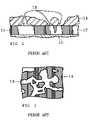
- FIG. 2shows a top view of a contact layer 14 with gaps 18 .
- spikingAnother problem arising with the formation of a contact directly on a wide band-gap material is spiking, particularly when contact is made to thin layers of wide band-gap material. As shown in FIG. 1 , spiking can create an electrical short when the contact region 16 extends entirely through a layer of wide band-gap material 12 to an underlying substrate 10 .
- Barrier layers between the contact metal and wide band-gap materialhave been used to prevent spiking of the wide band-gap material by the contact material during annealing processes.
- these layersadd additional processing steps and generally increase the resistivity of the electrical connection between the contact and wide band-gap material.
- an annealing stepis required to create an ohmic contact between the contact metal and the barrier layer, problems regarding the melting and separation of the contact metal still exist and reduce the contact quality.
- the processmay overcome the problems above by enabling the manufacture of uniform ohmic electrical contacts between SiC and a low melting point material using conventional semiconductor processes.
- Ohmic contactsmay be produced using longer, lower temperature anneals and fewer processing stages than prior techniques.
- a semiconductor devicecan comprise a silicon carbide region having a contact area.
- the silicon carbide regionmay comprise p-type silicon carbide.
- the contact areamay comprise a substantially uniform and continuous contact region throughout the contact area.
- the contact regioncan comprise an aluminum-silicon carbide alloy.
- a low melting point contact materialmay be in direct and substantially continuous contact with the contact region.
- the low melting point contact materialmay have a melting point at or below approximately 700 degrees Celsius. Electrical contact between the contact material and SiC region may be ohmic.
- a process for forming an electrical connection to a semiconductor devicecan comprise forming an exposed region that includes silicon carbide.
- the processcan also comprise forming a first metal-containing layer that contacts the exposed region.
- the first metal-containing layermay comprise a composition that does not form an ohmic contact with a doped silicon carbide if annealed for a time period of less than five hours and at a temperature less than the melting point of a material within the metal-containing layer.
- the processmay further comprise annealing the metal-containing layer and exposed region until a substantially continuous ohmic contact region is formed between the first metal-containing layer and the silicon carbide.
- a process for forming an electrical connection to a semiconductor devicecan comprise forming an exposed region that includes silicon carbide.
- the processcan also comprise forming a metal-containing layer that contacts the exposed region.
- the processmay further comprise annealing the metal-containing layer and exposed region for a time period of at least approximately ten hours and at a temperature of at least approximately 300 C.
- FIG. 1includes an illustration of a cross-sectional view of a portion of a prior art contact where a high temperature anneal has caused the contact layer to melt resulting in discontinuities in the contact region.
- FIG. 2includes an illustration of a top view of a portion of the prior art contact of FIG. 1 .
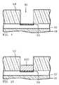
- FIG. 3includes an illustration of a cross-sectional view of a portion of a contact between a contact layer and a wide band-gap semiconductor material.
- FIG. 4includes an illustration of a cross-sectional view of a portion of the material of FIG. 3 after the contact layer has been etched.
- FIG. 5includes an illustration of a cross-sectional view of a portion of the material of FIG. 4 after annealing has formed contact regions between the contact layer and wide band-gap semiconductor.
- FIG. 6includes an illustration of a cross-sectional view of a portion of the material of FIG. 5 after forming an insulating layer over the contact layer and wide band-gap semiconductor material.
- FIG. 7includes an enlarged illustration of a cross-sectional view of the material of FIG. 6 after etching a portion of the insulating layer to expose portions of the contact layer.
- FIG. 8includes an illustration of a cross-sectional view of a portion of the material of FIG. 7 where portions of the insulating layer have been removed to expose the contact region.
- FIG. 9includes an illustration of a cross-sectional view of a portion of the device of FIG. 8 after removing the contact layer.
- FIG. 10includes an illustration of a cross-sectional view of a portion of the device FIG. 9 after forming a second contact layer.
- a non-ohmic contactmay be annealed at a temperature less than the melting point of a material within the contact layer. Annealing may take more than two hours.
- An ohmic contact regioncan be substantially continuous and may not have discontinuities due to melting, balling, peeling, or other destructive mechanisms.
- FIG. 3illustrates a contact layer 34 formed over a large band gap semiconductor material 32 and an underlying substrate 30 .
- the contact layer 34may comprise a low melting point material that has a melting point less than approximately 700 degrees Celsius, such as aluminum, zinc, or the like.
- the contact layer 34can comprise a substantially pure material or can comprise a material with impurities. Impurities in the contact layer 34 may comprise less than ten weight percent of the contact layer 34 .
- the contact layer 34can be formed through sputtering, chemical vapor deposition, or another conventional deposition processes and may generally be deposited to a thickness of approximately twenty percent of the thickness of the underlying wide band-gap semiconductor material 32 .
- the contact layer 34may form a rectifying or otherwise non-ohmic connection to the wide band-gap semiconductor 32 upon deposition and before performing any anneals.
- a wide band-gap semiconductor material 32may be any semiconductor with a band-gap greater than approximately two electron volts, such as silicon carbide.
- the wide band-gap semiconductor material 32may comprise a P-type dopant such as boron, aluminum, or another similar dopant.
- the wide band-gap semiconductor thicknessmay be any thickness required by desired end product specification, but may generally fall within the range of approximately 0.1–100 microns, and more commonly in a range of approximately 0.1–4 microns.
- Material 32may be the base in a transistor.
- the contact layer 34 and wide band-gap semiconductor 32may be in direct and substantially continuous contact throughout the area over which the contact layer 34 is formed.
- the portion of the underlying substrate 30may comprise a wide band-gap semiconductor material. More particularly, the underlying substrate 30 may comprise silicon carbide and may comprise a dopant with a conductivity type opposite the conductivity type of the dopant of layer 32 such that a P-N or similar junction may be formed between substrate 30 and layer 32 .
- Layer 30may be a collector in a transistor.
- the contact layer 34can be used as a mask while etching the wide band-gap semiconductor material 32 . As illustrated in FIG. 4 , the contact layer 34 can be patterned and etched using conventional dry or wet methods to expose the underlying material. The contact layer 34 may be etched using common etchants, such as phosphoric acid or other similarly reactive chemicals. Features may be etched in the wide band-gap semiconductor material 32 using common methods, such as reactive ion etching with carbon tetrafluoride, sulfur hexafluoride, or other similarly reactive chemicals. The remaining portion of the contact layer 34 generally defines the contact area of the material 32 in this particular embodiment.
- the contact layer 34 and wide band-gap semiconductor material 32may be annealed to form a contact region 50 as illustrated in FIG. 5 .
- Annealingmay be performed at a temperature lower than the melting point of the contact layer 34 , for example less than approximately 700 degrees Celsius and generally in the range of approximately 400–660 degrees Celsius.
- Annealingmay be accomplished by maintaining the contact layer 34 and wide band-gap semiconductor material 32 at a selected annealing temperature for a duration of time sufficient to yield a contact region 50 with ohmic properties.
- the time periodmay be more than approximately ten hours and may generally be in the range of approximately 25–60 hours.
- Annealingmay be performed in an atmosphere comprising a substantially inert or noble gas, such as argon, or in a vacuum.
- the contact region 50may comprise an alloy of the contact layer 34 and wide band-gap semiconductor material 32 and form a substantially ohmic connection to be made between the material 32 and the contact layer 34 as shown in FIG. 5 .
- FIG. 5compare to FIG. 1 in which a contact layer 12 has suffered from balling, melting, and peeling as may happen when annealed at temperatures above the melting point of the contact layer 12 .
- the contact region 30 of the embodiment as illustrated in FIG. 5may be substantially continuous and free of significant discontinuities due to peeling, balling, melting, or other mechanisms that could affect the contact layer 34 during annealing. Additionally, the contact region 32 may not extend entirely through the wide band-gap semiconductor 10 to underlying layer 42 , causing an electrical short.
- An insulating material 60may be formed over the exposed contact region 50 , wide band-gap semiconductor 32 , and contact layer 34 , as illustrated in FIG. 6 .
- the insulating material 60may comprise an insulator such as silicon dioxide, silicon nitride, or another similar insulating material. Insulating material 60 can be formed using conventional processes including sputter deposition or chemical vapor deposition.
- the insulating material 60may be deposited to a thickness greater than that of the contact layer 34 , and may generally be between approximately 0.5–20 microns thick. Portions of the insulating material 60 can be removed to expose underlying portions of the contact layer 34 , as shown if FIG. 7 .
- the insulating materialmay be removed via common etch processes using hydrofluoric acid or another similar etchant. Mechanical removal such as polishing may be employed to form a planar structure as shown in FIG. 8 .
- the contact layer 34may be substantially entirely removed to expose the contact region 50 by etching with phosphoric acid or another similar etchant.
- a second contact layer 100shown in FIG. 10 , may be formed at least partially within the openings 90 and in contact with the contact region 50 .
- the second contact layer 100may comprise the same material as the first contact layer and may form a substantially ohmic electrical connection to the silicon carbide region 32 .
- the second contact layercan be formed through sputtering or other common deposition methods, and may have a thickness in the range of approximately 0.5–20 microns.
- a substantially complete electrical devicesuch as a diode or transistor, may be formed by connecting wires, leads, or other similar apparatus (not shown) to the exposed contact layer 34 portions.
- wires, leads, or other similar apparatuscould be formed over or from a portion of material 32 .
- Wires, leads, or other apparatuscan be bonded, soldered, or otherwise electrically connected to the exposed contact layer 34 portions.
- devices producedcan exhibit lower contact resistance due to the substantially continuous contact region.
- Lower contact resistancecan result in faster and more efficient and reliable operation of devices.
- Production costs for these devicesmay also be reduced due to the greater reproducibility and yields that can be realized with the uniform contact region.
- Devices produced accordinglydo not require barrier layers or thick semiconductor layers to prevent spiking.
- the terms “comprises,” “comprising,” “includes,” “including,” “has,” “having” or any other variation thereof,are intended to cover a non-exclusive inclusion.
- a process, method, article, or apparatus that comprises a list of elementsis not necessarily limited only those elements but may include other elements not expressly listed or inherent to such process, method, article, or apparatus.
- “or”refers to an inclusive or and not to an exclusive or. In one example, a condition A or B is satisfied by any one of the following: A is true (or present) and B is false (or not present), A is false (or not present) and B is true (or present), and both A and B are true (or present).
Landscapes
- Engineering & Computer Science (AREA)
- Chemical & Material Sciences (AREA)
- Crystallography & Structural Chemistry (AREA)
- Physics & Mathematics (AREA)
- Condensed Matter Physics & Semiconductors (AREA)
- General Physics & Mathematics (AREA)
- Manufacturing & Machinery (AREA)
- Computer Hardware Design (AREA)
- Microelectronics & Electronic Packaging (AREA)
- Power Engineering (AREA)
- Electrodes Of Semiconductors (AREA)
Abstract
Description
Claims (22)
Priority Applications (4)
| Application Number | Priority Date | Filing Date | Title |
|---|---|---|---|
| US10/029,101US6955978B1 (en) | 2001-12-20 | 2001-12-20 | Uniform contact |
| DE10259292.6ADE10259292B4 (en) | 2001-12-20 | 2002-12-18 | Method for producing a uniform contact and uniform contact made therewith |
| JP2002369665AJP4824896B2 (en) | 2001-12-20 | 2002-12-20 | Method for forming an electrical connection in a semiconductor device |
| US11/190,654US7411219B2 (en) | 2001-12-20 | 2005-07-27 | Uniform contact |
Applications Claiming Priority (1)
| Application Number | Priority Date | Filing Date | Title |
|---|---|---|---|
| US10/029,101US6955978B1 (en) | 2001-12-20 | 2001-12-20 | Uniform contact |
Related Child Applications (1)
| Application Number | Title | Priority Date | Filing Date |
|---|---|---|---|
| US11/190,654DivisionUS7411219B2 (en) | 2001-12-20 | 2005-07-27 | Uniform contact |
Publications (1)
| Publication Number | Publication Date |
|---|---|
| US6955978B1true US6955978B1 (en) | 2005-10-18 |
Family
ID=21847214
Family Applications (2)
| Application Number | Title | Priority Date | Filing Date |
|---|---|---|---|
| US10/029,101Expired - Fee RelatedUS6955978B1 (en) | 2001-12-20 | 2001-12-20 | Uniform contact |
| US11/190,654Expired - LifetimeUS7411219B2 (en) | 2001-12-20 | 2005-07-27 | Uniform contact |
Family Applications After (1)
| Application Number | Title | Priority Date | Filing Date |
|---|---|---|---|
| US11/190,654Expired - LifetimeUS7411219B2 (en) | 2001-12-20 | 2005-07-27 | Uniform contact |
Country Status (3)
| Country | Link |
|---|---|
| US (2) | US6955978B1 (en) |
| JP (1) | JP4824896B2 (en) |
| DE (1) | DE10259292B4 (en) |
Cited By (2)
| Publication number | Priority date | Publication date | Assignee | Title |
|---|---|---|---|---|
| US20070015308A1 (en)* | 2004-07-15 | 2007-01-18 | Fairchild Semiconductor Corporation | Schottky diode structure to reduce capacitance and switching losses and method of making same |
| US20220262905A1 (en)* | 2021-02-17 | 2022-08-18 | Fuji Electric Co., Ltd. | Silicon carbide semiconductor device and method of manufacturing silicon carbide semiconductor device |
Families Citing this family (3)
| Publication number | Priority date | Publication date | Assignee | Title |
|---|---|---|---|---|
| US20050215041A1 (en)* | 2004-03-23 | 2005-09-29 | Seng William F | Low temperature, long term annealing of nickel contacts to lower interfacial resistance |
| US9711633B2 (en) | 2008-05-09 | 2017-07-18 | Cree, Inc. | Methods of forming group III-nitride semiconductor devices including implanting ions directly into source and drain regions and annealing to activate the implanted ions |
| US9099578B2 (en)* | 2012-06-04 | 2015-08-04 | Nusola, Inc. | Structure for creating ohmic contact in semiconductor devices and methods for manufacture |
Citations (21)
| Publication number | Priority date | Publication date | Assignee | Title |
|---|---|---|---|---|
| US3900598A (en)* | 1972-03-13 | 1975-08-19 | Motorola Inc | Ohmic contacts and method of producing same |
| US3965279A (en)* | 1974-09-03 | 1976-06-22 | Bell Telephone Laboratories, Incorporated | Ohmic contacts for group III-V n-type semiconductors |
| US4301592A (en)* | 1978-05-26 | 1981-11-24 | Hung Chang Lin | Method of fabricating semiconductor junction device employing separate metallization |
| JPS59214224A (en)* | 1983-05-20 | 1984-12-04 | Sanyo Electric Co Ltd | Electrode formation of sic |
| US4602421A (en)* | 1985-04-24 | 1986-07-29 | The United States Of America As Represented By The Secretary Of The Air Force | Low noise polycrystalline semiconductor resistors by hydrogen passivation |
| JPS6420616A (en)* | 1987-07-15 | 1989-01-24 | Sanyo Electric Co | Formation of p-type sic electrode |
| US5070027A (en)* | 1989-02-23 | 1991-12-03 | Matsushita Electric Industrial Co., Ltd. | Method of forming a heterostructure diode |
| US5250466A (en)* | 1991-04-29 | 1993-10-05 | Telefunken Electronic Gmbh | Method for manufacturing ohmic contacts for compound semiconductors |
| US5416342A (en)* | 1993-06-23 | 1995-05-16 | Cree Research, Inc. | Blue light-emitting diode with high external quantum efficiency |
| US5485019A (en) | 1992-02-05 | 1996-01-16 | Semiconductor Energy Laboratory Co., Ltd. | Semiconductor device and method for forming the same |
| US5502003A (en)* | 1994-03-04 | 1996-03-26 | Fuji Electric Co., Ltd. | Silicon carbide electronic device manufacturing method |
| US5635412A (en)* | 1994-05-04 | 1997-06-03 | North Carolina State University | Methods of fabricating voltage breakdown resistant monocrystalline silicon carbide semiconductor devices |
| US5668382A (en)* | 1993-09-08 | 1997-09-16 | Sumitomo Electric Industries, Ltd. | Ohmic electrode and method for forming it |
| US5980265A (en)* | 1994-06-03 | 1999-11-09 | Advanced Technology Materials, Inc. | Low resistance, stable ohmic contacts to silicon carbide, and method of making the same |
| US20020052102A1 (en)* | 2000-08-31 | 2002-05-02 | Nissan Motor Co., Ltd. | Method for manufacturing silicon carbide device and oxidation furnace |
| US20020125482A1 (en)* | 1999-09-22 | 2002-09-12 | Peter Friedrichs | Semiconductor device made from silicon carbide with a schottky contact and an ohmic contact made from a nickel-aluminum material and process for producing the semiconductor device |
| US6468890B2 (en)* | 1998-09-02 | 2002-10-22 | Siced Electronics Development Gmbh & Co. Kg | Semiconductor device with ohmic contact-connection and method for the ohmic contact-connection of a semiconductor device |
| US20020179910A1 (en)* | 2001-03-15 | 2002-12-05 | Slater David B. | Low temperature formation of backside ohmic contacts for vertical devices |
| US20030034495A1 (en)* | 2001-07-12 | 2003-02-20 | Casady Jeffrey B. | Self-aligned transistor and diode topologies in silicon carbide through the use of selective epitaxy or selective implantation |
| US6599644B1 (en)* | 2000-10-06 | 2003-07-29 | Foundation For Research & Technology-Hellas | Method of making an ohmic contact to p-type silicon carbide, comprising titanium carbide and nickel silicide |
| US20040171204A1 (en)* | 2001-03-15 | 2004-09-02 | Slater David B. | Low temperature formation of backside ohmic contacts for vertical devices |
Family Cites Families (17)
| Publication number | Priority date | Publication date | Assignee | Title |
|---|---|---|---|---|
| US3982262A (en)* | 1974-04-17 | 1976-09-21 | Karatsjuba Anatoly Prokofievic | Semiconductor indicating instrument |
| JP2708798B2 (en)* | 1988-08-05 | 1998-02-04 | 三洋電機株式会社 | Method of forming electrode of silicon carbide |
| JPH0383332A (en)* | 1989-08-28 | 1991-04-09 | Sharp Corp | Manufacture of silicon carbide semiconductor device |
| JP2908001B2 (en)* | 1990-11-21 | 1999-06-21 | 日本電気株式会社 | Semiconductor device |
| US5264713A (en)* | 1991-06-14 | 1993-11-23 | Cree Research, Inc. | Junction field-effect transistor formed in silicon carbide |
| JP3036138B2 (en)* | 1991-07-31 | 2000-04-24 | 信越半導体株式会社 | Method for manufacturing compound semiconductor electronic device |
| JPH0567808A (en)* | 1991-09-06 | 1993-03-19 | Sanyo Electric Co Ltd | Formation of electrode of sic light emitting diode |
| JPH065722A (en)* | 1992-06-16 | 1994-01-14 | Nec Corp | Manufacture of semiconductor integrated circuit device |
| US5323022A (en)* | 1992-09-10 | 1994-06-21 | North Carolina State University | Platinum ohmic contact to p-type silicon carbide |
| US5539217A (en)* | 1993-08-09 | 1996-07-23 | Cree Research, Inc. | Silicon carbide thyristor |
| US5661312A (en)* | 1995-03-30 | 1997-08-26 | Motorola | Silicon carbide MOSFET |
| JPH11274469A (en)* | 1998-03-25 | 1999-10-08 | Mitsubishi Chemical Corp | III-V compound semiconductor device |
| JP3439123B2 (en)* | 1998-06-18 | 2003-08-25 | 古河電気工業株式会社 | Ohmic electrode |
| EP1248302B1 (en)* | 1999-12-21 | 2012-09-26 | Sumitomo Electric Industries, Ltd. | Horizontal junction field-effect transistor |
| JP2002122560A (en)* | 2000-08-10 | 2002-04-26 | Ngk Spark Plug Co Ltd | Gas sensor |
| DE10051049B4 (en)* | 2000-10-14 | 2011-04-07 | Cree, Inc. | Aluminum-nickel contact metallization for p-doped SiC and manufacturing process therefor |
| US7132701B1 (en)* | 2001-07-27 | 2006-11-07 | Fairchild Semiconductor Corporation | Contact method for thin silicon carbide epitaxial layer and semiconductor devices formed by those methods |
- 2001
- 2001-12-20USUS10/029,101patent/US6955978B1/ennot_activeExpired - Fee Related
- 2002
- 2002-12-18DEDE10259292.6Apatent/DE10259292B4/ennot_activeExpired - Fee Related
- 2002-12-20JPJP2002369665Apatent/JP4824896B2/ennot_activeExpired - Lifetime
- 2005
- 2005-07-27USUS11/190,654patent/US7411219B2/ennot_activeExpired - Lifetime
Patent Citations (21)
| Publication number | Priority date | Publication date | Assignee | Title |
|---|---|---|---|---|
| US3900598A (en)* | 1972-03-13 | 1975-08-19 | Motorola Inc | Ohmic contacts and method of producing same |
| US3965279A (en)* | 1974-09-03 | 1976-06-22 | Bell Telephone Laboratories, Incorporated | Ohmic contacts for group III-V n-type semiconductors |
| US4301592A (en)* | 1978-05-26 | 1981-11-24 | Hung Chang Lin | Method of fabricating semiconductor junction device employing separate metallization |
| JPS59214224A (en)* | 1983-05-20 | 1984-12-04 | Sanyo Electric Co Ltd | Electrode formation of sic |
| US4602421A (en)* | 1985-04-24 | 1986-07-29 | The United States Of America As Represented By The Secretary Of The Air Force | Low noise polycrystalline semiconductor resistors by hydrogen passivation |
| JPS6420616A (en)* | 1987-07-15 | 1989-01-24 | Sanyo Electric Co | Formation of p-type sic electrode |
| US5070027A (en)* | 1989-02-23 | 1991-12-03 | Matsushita Electric Industrial Co., Ltd. | Method of forming a heterostructure diode |
| US5250466A (en)* | 1991-04-29 | 1993-10-05 | Telefunken Electronic Gmbh | Method for manufacturing ohmic contacts for compound semiconductors |
| US5485019A (en) | 1992-02-05 | 1996-01-16 | Semiconductor Energy Laboratory Co., Ltd. | Semiconductor device and method for forming the same |
| US5416342A (en)* | 1993-06-23 | 1995-05-16 | Cree Research, Inc. | Blue light-emitting diode with high external quantum efficiency |
| US5668382A (en)* | 1993-09-08 | 1997-09-16 | Sumitomo Electric Industries, Ltd. | Ohmic electrode and method for forming it |
| US5502003A (en)* | 1994-03-04 | 1996-03-26 | Fuji Electric Co., Ltd. | Silicon carbide electronic device manufacturing method |
| US5635412A (en)* | 1994-05-04 | 1997-06-03 | North Carolina State University | Methods of fabricating voltage breakdown resistant monocrystalline silicon carbide semiconductor devices |
| US5980265A (en)* | 1994-06-03 | 1999-11-09 | Advanced Technology Materials, Inc. | Low resistance, stable ohmic contacts to silicon carbide, and method of making the same |
| US6468890B2 (en)* | 1998-09-02 | 2002-10-22 | Siced Electronics Development Gmbh & Co. Kg | Semiconductor device with ohmic contact-connection and method for the ohmic contact-connection of a semiconductor device |
| US20020125482A1 (en)* | 1999-09-22 | 2002-09-12 | Peter Friedrichs | Semiconductor device made from silicon carbide with a schottky contact and an ohmic contact made from a nickel-aluminum material and process for producing the semiconductor device |
| US20020052102A1 (en)* | 2000-08-31 | 2002-05-02 | Nissan Motor Co., Ltd. | Method for manufacturing silicon carbide device and oxidation furnace |
| US6599644B1 (en)* | 2000-10-06 | 2003-07-29 | Foundation For Research & Technology-Hellas | Method of making an ohmic contact to p-type silicon carbide, comprising titanium carbide and nickel silicide |
| US20020179910A1 (en)* | 2001-03-15 | 2002-12-05 | Slater David B. | Low temperature formation of backside ohmic contacts for vertical devices |
| US20040171204A1 (en)* | 2001-03-15 | 2004-09-02 | Slater David B. | Low temperature formation of backside ohmic contacts for vertical devices |
| US20030034495A1 (en)* | 2001-07-12 | 2003-02-20 | Casady Jeffrey B. | Self-aligned transistor and diode topologies in silicon carbide through the use of selective epitaxy or selective implantation |
Non-Patent Citations (7)
| Title |
|---|
| "Aluminum Doped 6H SiC: CVD Growth and Formation of Ohmic Contacts", Inst. Phys. Conf. Seri No. 196, 1996 IOP Publishing Ltd. |
| "Interface Chemistry and Electrical Properties of Annealed NI and Ni/Al-6H SiC Structures", C. Halling, R. Yakimova, V. Krastve, Ts. Marinova and E. Janzen, Inst. Phys. Conf. Seri No. 196, 1996 IOP Publishing Ltd. |
| "Specific Contact Resistance as a Function of Doping N-type 4H and 6H-SiC", Inst. Phys. Conf. Seri No. 196, 1996 IOP Publishing Ltd. |
| "The Influence of Dry Cleaning Techniques on Thermal Oxides Grown on 4H and 6H P-type SiC", C.-M. Zetterling, C.I. Harris, M. Ostling and V.V. Afanas'ev, Inst. Phys. Conf. Seri No. 196, 1996 IOP Publishing Ltd. |
| A. E. Nomura et al., "Ohmic Contact Formation on N-Type 6H-SiC Using polysilicon and Silicides", Semiconductor Device Research Symposium, 2001 International, Dec. 5-7, 2001, Page(s): 523-526.* |
| D. Alok et al., "Low contact resistivity ohmic contacts to 6H-silicon carbide", Electron Devices Meeting, 1993. Technical Digest., International, Dec. 5-8, 1993, Page(s): 691-694.* |
| VLSI Technology, "Junction Spiking," McGraw-Hill Book Company, pp. 367-369,1983. |
Cited By (4)
| Publication number | Priority date | Publication date | Assignee | Title |
|---|---|---|---|---|
| US20070015308A1 (en)* | 2004-07-15 | 2007-01-18 | Fairchild Semiconductor Corporation | Schottky diode structure to reduce capacitance and switching losses and method of making same |
| US7468314B2 (en)* | 2004-07-15 | 2008-12-23 | Fairchild Semiconductor Corporation | Schottky diode structure to reduce capacitance and switching losses and method of making same |
| US20220262905A1 (en)* | 2021-02-17 | 2022-08-18 | Fuji Electric Co., Ltd. | Silicon carbide semiconductor device and method of manufacturing silicon carbide semiconductor device |
| US12080762B2 (en)* | 2021-02-17 | 2024-09-03 | Fuji Electric Co., Ltd. | Silicon carbide semiconductor device and method of manufacturing silicon carbide semiconductor device |
Also Published As
| Publication number | Publication date |
|---|---|
| JP4824896B2 (en) | 2011-11-30 |
| US20050269574A1 (en) | 2005-12-08 |
| US7411219B2 (en) | 2008-08-12 |
| JP2003209067A (en) | 2003-07-25 |
| DE10259292A1 (en) | 2003-07-10 |
| DE10259292B4 (en) | 2014-01-23 |
Similar Documents
| Publication | Publication Date | Title |
|---|---|---|
| US4206540A (en) | Schottky device and method of manufacture using palladium and platinum intermetallic alloys and titanium barrier | |
| US2796562A (en) | Semiconductive device and method of fabricating same | |
| US4263058A (en) | Composite conductive structures in integrated circuits and method of making same | |
| US4227944A (en) | Methods of making composite conductive structures in integrated circuits | |
| US4408216A (en) | Schottky device and method of manufacture using palladium and platinum intermetallic alloys and titanium barrier for low reverse leakage over wide temperature range | |
| JPS60201666A (en) | semiconductor equipment | |
| USRE42423E1 (en) | Contact method for thin silicon carbide epitaxial layer and semiconductor devices formed by those methods | |
| US4228212A (en) | Composite conductive structures in integrated circuits | |
| US6955978B1 (en) | Uniform contact | |
| US5751067A (en) | Compact semiconductor device having excellent electrical characteristics and long time reliability | |
| JPS6364057B2 (en) | ||
| US3956820A (en) | Method of manufacturing a semiconductor device having a lead bonded to a surface thereof | |
| EP0303390B1 (en) | Manufacture of diodes | |
| JPH08255769A (en) | Method for manufacturing semiconductor device | |
| CN114284413B (en) | Electrode manufacturing method of semiconductor device and semiconductor device | |
| US4871617A (en) | Ohmic contacts and interconnects to silicon and method of making same | |
| JPH0837289A (en) | Semiconductor device and manufacture thereof | |
| JPH0757904A (en) | Diamond semiconductor device | |
| JPH0864801A (en) | Silicon carbide semiconductor device and method for manufacturing the same | |
| EP0249256A2 (en) | A semiconductor device with an aluminium interconnect layer containing a small percentage of vanadium | |
| KR900000442B1 (en) | Aluminum metallization layer formed on silicon wafer and its manufacturing method | |
| KR0161774B1 (en) | Semiconductor device and manufacturing method | |
| JPH04274374A (en) | Solar cells and their manufacturing method | |
| JPH1168048A (en) | Semiconductor device and forming method thereof | |
| JP2002261044A (en) | Semiconductor device and method of manufacturing the same |
Legal Events
| Date | Code | Title | Description |
|---|---|---|---|
| AS | Assignment | Owner name:EXTREME DEVICES, INC., TEXAS Free format text:ASSIGNMENT OF ASSIGNORS INTEREST;ASSIGNORS:WOODIN, RICHARD L.;SENG, WILLIAM F.;REEL/FRAME:012479/0404 Effective date:20011214 | |
| AS | Assignment | Owner name:FAIRCHILD SEMICONDUCTOR CORPORATION, MAINE Free format text:ASSIGNMENT OF ASSIGNORS INTEREST;ASSIGNOR:EXTREME DEVICES, INC.;REEL/FRAME:013159/0499 Effective date:20020501 | |
| FPAY | Fee payment | Year of fee payment:4 | |
| FPAY | Fee payment | Year of fee payment:8 | |
| AS | Assignment | Owner name:DEUTSCHE BANK AG NEW YORK BRANCH, AS COLLATERAL AGENT, NEW YORK Free format text:PATENT SECURITY AGREEMENT;ASSIGNOR:FAIRCHILD SEMICONDUCTOR CORPORATION;REEL/FRAME:040075/0644 Effective date:20160916 Owner name:DEUTSCHE BANK AG NEW YORK BRANCH, AS COLLATERAL AG Free format text:PATENT SECURITY AGREEMENT;ASSIGNOR:FAIRCHILD SEMICONDUCTOR CORPORATION;REEL/FRAME:040075/0644 Effective date:20160916 | |
| REMI | Maintenance fee reminder mailed | ||
| LAPS | Lapse for failure to pay maintenance fees | Free format text:PATENT EXPIRED FOR FAILURE TO PAY MAINTENANCE FEES (ORIGINAL EVENT CODE: EXP.) | |
| STCH | Information on status: patent discontinuation | Free format text:PATENT EXPIRED DUE TO NONPAYMENT OF MAINTENANCE FEES UNDER 37 CFR 1.362 | |
| FP | Lapsed due to failure to pay maintenance fee | Effective date:20171018 | |
| AS | Assignment | Owner name:FAIRCHILD SEMICONDUCTOR CORPORATION, ARIZONA Free format text:RELEASE BY SECURED PARTY;ASSIGNOR:DEUTSCHE BANK AG NEW YORK BRANCH;REEL/FRAME:057969/0206 Effective date:20211027 | |
| AS | Assignment | Owner name:DEUTSCHE BANK AG NEW YORK BRANCH, AS COLLATERAL AGENT, NEW YORK Free format text:SECURITY INTEREST;ASSIGNOR:SEMICONDUCTOR COMPONENTS INDUSTRIES, LLC;REEL/FRAME:058871/0799 Effective date:20211028 | |
| AS | Assignment | Owner name:FAIRCHILD SEMICONDUCTOR CORPORATION, ARIZONA Free format text:RELEASE OF SECURITY INTEREST IN PATENTS RECORDED AT REEL 040075, FRAME 0644;ASSIGNOR:DEUTSCHE BANK AG NEW YORK BRANCH, AS COLLATERAL AGENT;REEL/FRAME:064070/0536 Effective date:20230622 Owner name:SEMICONDUCTOR COMPONENTS INDUSTRIES, LLC, ARIZONA Free format text:RELEASE OF SECURITY INTEREST IN PATENTS RECORDED AT REEL 040075, FRAME 0644;ASSIGNOR:DEUTSCHE BANK AG NEW YORK BRANCH, AS COLLATERAL AGENT;REEL/FRAME:064070/0536 Effective date:20230622 | |
| AS | Assignment | Owner name:FAIRCHILD SEMICONDUCTOR CORPORATION, ARIZONA Free format text:RELEASE OF SECURITY INTEREST IN PATENTS RECORDED AT REEL 058871, FRAME 0799;ASSIGNOR:DEUTSCHE BANK AG NEW YORK BRANCH, AS COLLATERAL AGENT;REEL/FRAME:065653/0001 Effective date:20230622 Owner name:SEMICONDUCTOR COMPONENTS INDUSTRIES, LLC, ARIZONA Free format text:RELEASE OF SECURITY INTEREST IN PATENTS RECORDED AT REEL 058871, FRAME 0799;ASSIGNOR:DEUTSCHE BANK AG NEW YORK BRANCH, AS COLLATERAL AGENT;REEL/FRAME:065653/0001 Effective date:20230622 |