US6955931B1 - Method for detecting silicide encroachment of a gate electrode in a semiconductor arrangement - Google Patents
Method for detecting silicide encroachment of a gate electrode in a semiconductor arrangementDownload PDFInfo
- Publication number
- US6955931B1 US6955931B1US11/053,863US5386305AUS6955931B1US 6955931 B1US6955931 B1US 6955931B1US 5386305 AUS5386305 AUS 5386305AUS 6955931 B1US6955931 B1US 6955931B1
- Authority
- US
- United States
- Prior art keywords
- silicide
- gate electrode
- sidewall spacers
- substrate
- monitoring
- Prior art date
- Legal status (The legal status is an assumption and is not a legal conclusion. Google has not performed a legal analysis and makes no representation as to the accuracy of the status listed.)
- Expired - Lifetime
Links
- 229910021332silicideInorganic materials0.000titleclaimsabstractdescription64
- FVBUAEGBCNSCDD-UHFFFAOYSA-Nsilicide(4-)Chemical compound[Si-4]FVBUAEGBCNSCDD-UHFFFAOYSA-N0.000titleclaimsabstractdescription64
- 238000000034methodMethods0.000titleclaimsabstractdescription32
- 239000004065semiconductorSubstances0.000titleclaimsdescription18
- 125000006850spacer groupChemical group0.000claimsabstractdescription55
- 238000012544monitoring processMethods0.000claimsabstractdescription32
- 230000015572biosynthetic processEffects0.000claimsabstractdescription11
- 239000000758substrateSubstances0.000claimsdescription30
- 230000003287optical effectEffects0.000claimsdescription8
- 238000004519manufacturing processMethods0.000claimsdescription7
- 238000001312dry etchingMethods0.000claimsdescription3
- 238000001039wet etchingMethods0.000claimsdescription3
- 229910021334nickel silicideInorganic materials0.000claimsdescription2
- RUFLMLWJRZAWLJ-UHFFFAOYSA-Nnickel silicideChemical group[Ni]=[Si]=[Ni]RUFLMLWJRZAWLJ-UHFFFAOYSA-N0.000claimsdescription2
- 238000001514detection methodMethods0.000abstractdescription6
- 238000000926separation methodMethods0.000abstractdescription2
- 238000012545processingMethods0.000description7
- 239000010410layerSubstances0.000description5
- 239000000463materialSubstances0.000description5
- 229910052751metalInorganic materials0.000description5
- 239000002184metalSubstances0.000description5
- XUIMIQQOPSSXEZ-UHFFFAOYSA-NSiliconChemical compound[Si]XUIMIQQOPSSXEZ-UHFFFAOYSA-N0.000description4
- 230000000694effectsEffects0.000description4
- 229910052710siliconInorganic materials0.000description4
- 239000010703siliconSubstances0.000description4
- 238000012360testing methodMethods0.000description4
- 238000009792diffusion processMethods0.000description3
- 238000005468ion implantationMethods0.000description3
- 229910021420polycrystalline siliconInorganic materials0.000description3
- 229920005591polysiliconPolymers0.000description3
- PXHVJJICTQNCMI-UHFFFAOYSA-NNickelChemical compound[Ni]PXHVJJICTQNCMI-UHFFFAOYSA-N0.000description2
- 229910052581Si3N4Inorganic materials0.000description2
- VYPSYNLAJGMNEJ-UHFFFAOYSA-NSilicium dioxideChemical compoundO=[Si]=OVYPSYNLAJGMNEJ-UHFFFAOYSA-N0.000description2
- 230000008901benefitEffects0.000description2
- 150000004767nitridesChemical class0.000description2
- BASFCYQUMIYNBI-UHFFFAOYSA-NplatinumChemical compound[Pt]BASFCYQUMIYNBI-UHFFFAOYSA-N0.000description2
- 239000003870refractory metalSubstances0.000description2
- HQVNEWCFYHHQES-UHFFFAOYSA-Nsilicon nitrideChemical compoundN12[Si]34N5[Si]62N3[Si]51N64HQVNEWCFYHHQES-UHFFFAOYSA-N0.000description2
- 229910052814silicon oxideInorganic materials0.000description2
- RTAQQCXQSZGOHL-UHFFFAOYSA-NTitaniumChemical compound[Ti]RTAQQCXQSZGOHL-UHFFFAOYSA-N0.000description1
- 238000000137annealingMethods0.000description1
- 238000013459approachMethods0.000description1
- 230000000295complement effectEffects0.000description1
- 230000008021depositionEffects0.000description1
- 238000011161developmentMethods0.000description1
- 230000018109developmental processEffects0.000description1
- 239000007772electrode materialSubstances0.000description1
- 238000005530etchingMethods0.000description1
- 239000011229interlayerSubstances0.000description1
- 238000005259measurementMethods0.000description1
- 229910052759nickelInorganic materials0.000description1
- -1nickel silicideChemical compound0.000description1
- 229910052697platinumInorganic materials0.000description1
- 229910052719titaniumInorganic materials0.000description1
- 239000010936titaniumSubstances0.000description1
- WFKWXMTUELFFGS-UHFFFAOYSA-NtungstenChemical compound[W]WFKWXMTUELFFGS-UHFFFAOYSA-N0.000description1
- 229910052721tungstenInorganic materials0.000description1
- 239000010937tungstenSubstances0.000description1
Images


Classifications
- H—ELECTRICITY
- H10—SEMICONDUCTOR DEVICES; ELECTRIC SOLID-STATE DEVICES NOT OTHERWISE PROVIDED FOR
- H10D—INORGANIC ELECTRIC SEMICONDUCTOR DEVICES
- H10D30/00—Field-effect transistors [FET]
- H10D30/60—Insulated-gate field-effect transistors [IGFET]
- H10D30/791—Arrangements for exerting mechanical stress on the crystal lattice of the channel regions
- H—ELECTRICITY
- H01—ELECTRIC ELEMENTS
- H01L—SEMICONDUCTOR DEVICES NOT COVERED BY CLASS H10
- H01L22/00—Testing or measuring during manufacture or treatment; Reliability measurements, i.e. testing of parts without further processing to modify the parts as such; Structural arrangements therefor
- H01L22/20—Sequence of activities consisting of a plurality of measurements, corrections, marking or sorting steps
- H01L22/24—Optical enhancement of defects or not directly visible states, e.g. selective electrolytic deposition, bubbles in liquids, light emission, colour change
- H—ELECTRICITY
- H10—SEMICONDUCTOR DEVICES; ELECTRIC SOLID-STATE DEVICES NOT OTHERWISE PROVIDED FOR
- H10D—INORGANIC ELECTRIC SEMICONDUCTOR DEVICES
- H10D30/00—Field-effect transistors [FET]
- H10D30/01—Manufacture or treatment
- H10D30/021—Manufacture or treatment of FETs having insulated gates [IGFET]
- H10D30/0212—Manufacture or treatment of FETs having insulated gates [IGFET] using self-aligned silicidation
- H—ELECTRICITY
- H10—SEMICONDUCTOR DEVICES; ELECTRIC SOLID-STATE DEVICES NOT OTHERWISE PROVIDED FOR
- H10D—INORGANIC ELECTRIC SEMICONDUCTOR DEVICES
- H10D64/00—Electrodes of devices having potential barriers
- H10D64/01—Manufacture or treatment
- H10D64/015—Manufacture or treatment removing at least parts of gate spacers, e.g. disposable spacers
Definitions
- the present inventionrelates to manufacturing semiconductor devices, and more particularly, to the formation of silicide and detection of silicide encroachment in semiconductor arrangements.
- MOSmetal-oxide-semiconductor
- CMOScomplementary metal-oxide-semiconductor
- a gate electrodemay be formed over a semiconductor substrate with a gate dielectric layer therebetween and the sidewall spacers on side surfaces thereof.
- the sidewall spacerscan comprise silicon oxide, a silicon nitride or a silicon oxynitride, for example. Shallow source/drain extensions are typically formed using the gate electrode as a mask prior to forming these sidewall spacers.
- ion implantationis typically conducted using the gate electrode and sidewall spacers as a mask to form moderately- or heavily-doped and deeper source/drain regions.
- the thickness of the sidewall spacersis significant in at least two respects. Initially, the thickness of the sidewall spacer controls the length of the shallow source/drain extension. In addition, the width of the sidewall spacers controls the distance between the metal silicide layers and the side surfaces of the gate electrode.
- Silicidesuch as nickel silicide
- One problem with electrical testingis that the wafer has to be processed to metal 1 (M 1 ) before the electrical testing can be performed. This is wasteful of processing steps if the silicide encroachment has already rendered the part unusable.
- M 1metal 1
- embodiments of the present inventionwhich provide a method of detecting silicide encroachment of a gate electrode in a semiconductor arrangement comprising the steps of removing sidewall spacers on the gate electrode and a substrate, and performing line-of-sight monitoring of the substrate, after removal of the sidewall spacers, to detect silicide encroachment.
- the wayis cleared for performing line of sight monitoring of the substrate.
- Thispermits optical monitoring or electron microscope monitoring, for example, to be employed.
- silicide encroachmentis detected, unnecessary processing in the back end of the line (BEOL) can be avoided, if the encroachment is so great that the part would be unusable. This creates a cost saving in the manufacturing process.
- a method of manufacturing a semiconductor devicecomprising the steps of forming a gate electrode on a substrate and forming removable sidewalls spacers on the gate electrode and the substrate.
- Silicideis formed on the substrate, the sidewall spacers defining an offset of the silicide from the gate electrode.
- the sidewall spacersare removed to expose the substrate. Line-of-sight monitoring of the exposed substrate is performed to detect silicide encroachment.
- the earlier stated needsare also met by other aspects of the present invention which provide a method of monitoring a semiconductor arrangement.
- the methodcomprises the steps of forming silicide regions in a substrate, the silicide regions being offset from a gate electrode.
- the substrateis exposed at regions adjacent to the gate electrode.
- Line-of-sight monitoring of the exposed substrate regionsis performed to determine an amount of offset of the silicide regions from the gate electrode.
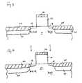
- FIG. 1is a schematic depiction of a cross-sectional view of a semiconductor device during one phase of manufacture in accordance with embodiments of the present invention.
- FIG. 2depicts the arrangement of FIG. 1 following the formation of silicide in accordance with embodiments of the present invention.
- FIG. 3depicts the arrangement of FIG. 2 after the sidewall spacers are removed in accordance with embodiments of the present invention.
- FIG. 4shows the arrangement of FIG. 3 during an observational phase in order to detect silicide encroachment in accordance with embodiments of the present invention.
- the present inventionaddresses and solves problems related to the detection of silicide encroachment of a gate electrode in a semiconductor arrangement, and in particular, to the obscuring of the silicide encroachment by sidewall spacers. This is achieved, at least in part, by the provision of the present invention for removal of sidewall spacers from the sidewalls of the gate electrode and from the substrate following silicide formation. This is followed by line-of-sight monitoring which can include either optical monitoring or electron microscope monitoring, for example. The observation allows for reliable detection of silicide encroachment. If the encroachment is so large that the device is unusable, further processing in the BEOL can be avoided, providing an overall cost savings.
- FIG. 1schematically depicts a cross-section of a semiconductor device during one phase of manufacturing in accordance with embodiments of the present invention.
- a gate electrode 12is provided on a substrate 10 , such as a silicon substrate, for example.
- sidewall spacers 16are formed on the sidewalls 14 of the gate electrode 12 by conventional methodologies.
- the gate electrode 12is made of polysilicon, for example, or other suitable material such as metal, silicide, etc.
- the sidewall spacers 16are made of a suitable material, such as silicon oxide, silicon nitride, silicon oxynitride, etc. As will be appreciated from the following description, the sidewall spacers 16 need to be made of material that is readily removable without damaging silicide or the gate electrode material.
- Source and drain extensions 18are formed by conventional ion implantation after the formation of the gate electrode 12 , but prior to the formation of the sidewalls spacer 16 . Formation of the source/drain extensions 18 can be accomplished by conventional ion implantation techniques and dosing amounts. Once the sidewall spacers 16 are formed, a heavier doping is performed to create the source and drain regions 20 . The sidewall spacer 16 and the gate electrode 12 serve to mask the substrate during the heavy or moderate doping processes.
- a silicide processhas been performed that creates silicide regions 22 , 24 in the source and drain regions 20 , respectively, and a silicide region 26 in the gate electrode 12 .
- Sidewall spacers 16prevent formation of the silicide on the gate electrode 12 , and the spacers 16 also initially precisely define the separation of the silicide regions 22 , 24 from the gate electrode 12 .
- a typical silicide processincludes the blanket deposition of a refractory metal, such as nickel, platinum, titanium, tungsten, etc., on the semiconductor wafer. An annealing process is performed that causes the silicide to form at the interface of the refractory metal and silicon.
- the silicidebe located at a precise distance from the gate electrode 12 .
- this distanceis X 1 .
- the silicide region 22 in FIG. 2is at this distance X 1 .
- the silicidedue to lateral diffusion, it is possible for the silicide to encroach toward the sidewalls 14 of the gate electrode 12 .
- thisis depicted as the encroachment of silicide region 24 towards the sidewall 14 of the gate electrode 12 .
- the distance X 2which is the distance from the left-most edge of the silicide region 24 to the right sidewall of the gate electrode 12 , is less than the desired distance X 1 (i.e., X 2 ⁇ X 1 ).
- This encroachmentmay be so great that the part becomes unusable. In such a case, if further processing occurs, the part will ultimately have to be discarded and the processing steps that followed the formation of silicide will have been wasted, increasing expense. It is therefore preferable to detect the encroachment of silicide at an earlier stage. However, detecting encroachment by electrical testing is difficult and can only be done after processing to metal 1 (M 1 ), and the spacers obscure a direct line-of-sight measurement.
- the sidewall spacers 16are removed by an appropriate etching technique, suitable for the material used in the sidewalls spacers 16 .
- a wet etching or dry etchingmay be employed, as appropriate, to complete remove the sidewall spacers 16 .
- the sidewall spacers 16may be safely removed at this time, since the sidewall spacers 16 have been employed to define the offset of the silicide from the gate edge, and have also already been employed in the doping process. The removal of the sidewall spacers 16 do not impact the device at this point in the flow.
- a line-of-sight monitoringcan now be performed to detect the silicide encroachment.
- the examples of line-of-sight monitoring techniquesinclude optical monitoring or electron microscope monitoring, for example. This achievable since the sidewall spacers 16 no longer obscure the substrate 10 directly adjacent to the gate electrode 12 . Hence, with this approach, the observation may be made in FIG. 4 that the silicide region 24 has undesirably encroached upon the sidewall 14 of the gate electrode 12 . It is to be noted that the depiction of FIGS. 3 and 4 of encroachment and no encroachment need not occur on the same gate, but is depicted in this manner for simplicity of explanation.
- the removal of the sidewall spacers 16enables bringing nitride etch shop layers for a contact inter-layer dielectric closer to the gate electrode 12 , in the steps following silicide formation.
- Recent developmentsemploy stressed nitride etch stop layers to enhance channel mobility in NMOS and PMOS devices by proper stress tuning.
Landscapes
- Engineering & Computer Science (AREA)
- Manufacturing & Machinery (AREA)
- Computer Hardware Design (AREA)
- Microelectronics & Electronic Packaging (AREA)
- Power Engineering (AREA)
- Insulated Gate Type Field-Effect Transistor (AREA)
- Electrodes Of Semiconductors (AREA)
Abstract
Description
Claims (17)
Priority Applications (1)
| Application Number | Priority Date | Filing Date | Title |
|---|---|---|---|
| US11/053,863US6955931B1 (en) | 2005-02-10 | 2005-02-10 | Method for detecting silicide encroachment of a gate electrode in a semiconductor arrangement |
Applications Claiming Priority (1)
| Application Number | Priority Date | Filing Date | Title |
|---|---|---|---|
| US11/053,863US6955931B1 (en) | 2005-02-10 | 2005-02-10 | Method for detecting silicide encroachment of a gate electrode in a semiconductor arrangement |
Publications (1)
| Publication Number | Publication Date |
|---|---|
| US6955931B1true US6955931B1 (en) | 2005-10-18 |
Family
ID=35066119
Family Applications (1)
| Application Number | Title | Priority Date | Filing Date |
|---|---|---|---|
| US11/053,863Expired - LifetimeUS6955931B1 (en) | 2005-02-10 | 2005-02-10 | Method for detecting silicide encroachment of a gate electrode in a semiconductor arrangement |
Country Status (1)
| Country | Link |
|---|---|
| US (1) | US6955931B1 (en) |
Cited By (3)
| Publication number | Priority date | Publication date | Assignee | Title |
|---|---|---|---|---|
| US20080268557A1 (en)* | 2007-04-24 | 2008-10-30 | Nanya Technology Corp. | Method for measuring a thin film thickness |
| EP2136405A1 (en)* | 2008-06-18 | 2009-12-23 | International Business Machines Corporation | Method and structure for SOI body contact FET with reduced parasitic capacitance |
| US20180076220A1 (en)* | 2016-09-09 | 2018-03-15 | International Business Machines Corporation | Conductive contacts in semiconductor on insulator substrate |
Citations (12)
| Publication number | Priority date | Publication date | Assignee | Title |
|---|---|---|---|---|
| US5780361A (en)* | 1995-06-23 | 1998-07-14 | Nec Corporation | Salicide process for selectively forming a monocobalt disilicide film on a silicon region |
| US5780362A (en)* | 1996-06-04 | 1998-07-14 | Wang; Qingfeng | CoSi2 salicide method |
| US6048791A (en)* | 1998-03-31 | 2000-04-11 | Kabushiki Kaisha Toshiba | Semiconductor device with electrode formed of conductive layer consisting of polysilicon layer and metal-silicide layer and its manufacturing method |
| US6251779B1 (en)* | 2000-06-01 | 2001-06-26 | United Microelectronics Corp. | Method of forming a self-aligned silicide on a semiconductor wafer |
| US20010041431A1 (en)* | 1999-03-18 | 2001-11-15 | Vlsi Technology, Inc. | Semiconductor device with transparent link area for silicide applications and fabrication thereof |
| US20020151170A1 (en)* | 1996-06-04 | 2002-10-17 | Karen Maex | Method of forming polycrystalline CoSi2 salicide and products obtained thereof |
| US20030003611A1 (en)* | 2001-06-29 | 2003-01-02 | Kla-Tencor Corporation | Apparatus and methods for monitoring self-aligned contact arrays |
| US20030077890A1 (en)* | 2001-10-24 | 2003-04-24 | Trivedi Jigish D. | Methods of forming conductive contacts |
| US6734099B2 (en)* | 2001-12-28 | 2004-05-11 | Texas Insturments Incorporated | System for preventing excess silicon consumption in ultra shallow junctions |
| US20040092045A1 (en)* | 2000-09-20 | 2004-05-13 | Gary Bultman | Methods and systems for determining a presence of macro and micro defects on a specimen |
| US6787464B1 (en)* | 2002-07-02 | 2004-09-07 | Advanced Micro Devices, Inc. | Method of forming silicide layers over a plurality of semiconductor devices |
| US6790683B1 (en)* | 2002-11-25 | 2004-09-14 | Advanced Micro Devices, Inc. | Methods of controlling wet chemical processes in forming metal silicide regions, and system for performing same |
- 2005
- 2005-02-10USUS11/053,863patent/US6955931B1/ennot_activeExpired - Lifetime
Patent Citations (12)
| Publication number | Priority date | Publication date | Assignee | Title |
|---|---|---|---|---|
| US5780361A (en)* | 1995-06-23 | 1998-07-14 | Nec Corporation | Salicide process for selectively forming a monocobalt disilicide film on a silicon region |
| US5780362A (en)* | 1996-06-04 | 1998-07-14 | Wang; Qingfeng | CoSi2 salicide method |
| US20020151170A1 (en)* | 1996-06-04 | 2002-10-17 | Karen Maex | Method of forming polycrystalline CoSi2 salicide and products obtained thereof |
| US6048791A (en)* | 1998-03-31 | 2000-04-11 | Kabushiki Kaisha Toshiba | Semiconductor device with electrode formed of conductive layer consisting of polysilicon layer and metal-silicide layer and its manufacturing method |
| US20010041431A1 (en)* | 1999-03-18 | 2001-11-15 | Vlsi Technology, Inc. | Semiconductor device with transparent link area for silicide applications and fabrication thereof |
| US6251779B1 (en)* | 2000-06-01 | 2001-06-26 | United Microelectronics Corp. | Method of forming a self-aligned silicide on a semiconductor wafer |
| US20040092045A1 (en)* | 2000-09-20 | 2004-05-13 | Gary Bultman | Methods and systems for determining a presence of macro and micro defects on a specimen |
| US20030003611A1 (en)* | 2001-06-29 | 2003-01-02 | Kla-Tencor Corporation | Apparatus and methods for monitoring self-aligned contact arrays |
| US20030077890A1 (en)* | 2001-10-24 | 2003-04-24 | Trivedi Jigish D. | Methods of forming conductive contacts |
| US6734099B2 (en)* | 2001-12-28 | 2004-05-11 | Texas Insturments Incorporated | System for preventing excess silicon consumption in ultra shallow junctions |
| US6787464B1 (en)* | 2002-07-02 | 2004-09-07 | Advanced Micro Devices, Inc. | Method of forming silicide layers over a plurality of semiconductor devices |
| US6790683B1 (en)* | 2002-11-25 | 2004-09-14 | Advanced Micro Devices, Inc. | Methods of controlling wet chemical processes in forming metal silicide regions, and system for performing same |
Cited By (7)
| Publication number | Priority date | Publication date | Assignee | Title |
|---|---|---|---|---|
| US20080268557A1 (en)* | 2007-04-24 | 2008-10-30 | Nanya Technology Corp. | Method for measuring a thin film thickness |
| EP2136405A1 (en)* | 2008-06-18 | 2009-12-23 | International Business Machines Corporation | Method and structure for SOI body contact FET with reduced parasitic capacitance |
| US20090315138A1 (en)* | 2008-06-18 | 2009-12-24 | International Business Machines Corporation | Method and structure for soi body contact fet with reduced parasitic capacitance |
| US7893494B2 (en) | 2008-06-18 | 2011-02-22 | International Business Machines Corporation | Method and structure for SOI body contact FET with reduced parasitic capacitance |
| US20180076220A1 (en)* | 2016-09-09 | 2018-03-15 | International Business Machines Corporation | Conductive contacts in semiconductor on insulator substrate |
| US10734410B2 (en)* | 2016-09-09 | 2020-08-04 | Elpis Technologies Inc. | Conductive contacts in semiconductor on insulator substrate |
| US11177285B2 (en) | 2016-09-09 | 2021-11-16 | Elpis Technologies Inc. | Conductive contacts in semiconductor on insulator substrate |
Similar Documents
| Publication | Publication Date | Title |
|---|---|---|
| US9147680B2 (en) | Integrated circuits having replacement metal gates with improved threshold voltage performance and methods for fabricating the same | |
| US9330980B2 (en) | Semiconductor process | |
| EP2149908B1 (en) | Replacement metal gate transistors with reduced gate oxide leakage | |
| US20070200179A1 (en) | Strain enhanced CMOS architecture with amorphous carbon film and fabrication method of forming the same | |
| US20060148152A1 (en) | Method of manufacturing semiconductor devices | |
| JP2002289700A (en) | Method for manufacturing dual gate of semiconductor device | |
| US8592951B2 (en) | Semiconductor wafer having W-shaped dummy metal filling section within monitor region | |
| CN100416763C (en) | Methods for Integrating High-K Gate Dielectrics in Transistor Processes | |
| CN105742353B (en) | MOS transistor and forming method thereof | |
| US6955931B1 (en) | Method for detecting silicide encroachment of a gate electrode in a semiconductor arrangement | |
| KR100934791B1 (en) | Semiconductor device for current characteristic measurement and current characteristic measurement method of semiconductor device | |
| US8390040B2 (en) | Localized spacer for a multi-gate transistor | |
| CN106816368B (en) | The forming method of semiconductor structure and CMOS transistor | |
| US7338910B2 (en) | Method of fabricating semiconductor devices and method of removing a spacer | |
| US20070275530A1 (en) | Semiconductor structure and fabricating method thereof | |
| US9117925B2 (en) | Epitaxial process | |
| US6358798B1 (en) | Method for forming gate electrode by damascene process | |
| US9184260B2 (en) | Methods for fabricating integrated circuits with robust gate electrode structure protection | |
| US20090042395A1 (en) | Spacer process for CMOS fabrication with bipolar transistor leakage prevention | |
| US11862670B2 (en) | Semiconductor device and method for manufacturing the same | |
| US20090020837A1 (en) | Semiconductor device and manufacturing method thereof | |
| KR20190120397A (en) | Manufacturing Method of Semiconductor Device | |
| KR20030087159A (en) | Semiconductor device and fabrication method thereof | |
| JP2000091564A (en) | Manufacture of semiconductor device | |
| JP2009267011A (en) | Method of manufacturing semiconductor device |
Legal Events
| Date | Code | Title | Description |
|---|---|---|---|
| AS | Assignment | Owner name:ADVANCED MICRO DEVICES, INC., CALIFORNIA Free format text:ASSIGNMENT OF ASSIGNORS INTEREST;ASSIGNORS:BROWN, DAVID E.;SUN, SEY-PING;REEL/FRAME:016269/0927 Effective date:20041022 | |
| STCF | Information on status: patent grant | Free format text:PATENTED CASE | |
| FPAY | Fee payment | Year of fee payment:4 | |
| AS | Assignment | Owner name:GLOBALFOUNDRIES INC., CAYMAN ISLANDS Free format text:AFFIRMATION OF PATENT ASSIGNMENT;ASSIGNOR:ADVANCED MICRO DEVICES, INC.;REEL/FRAME:023119/0083 Effective date:20090630 | |
| FPAY | Fee payment | Year of fee payment:8 | |
| FPAY | Fee payment | Year of fee payment:12 | |
| AS | Assignment | Owner name:WILMINGTON TRUST, NATIONAL ASSOCIATION, DELAWARE Free format text:SECURITY AGREEMENT;ASSIGNOR:GLOBALFOUNDRIES INC.;REEL/FRAME:049490/0001 Effective date:20181127 | |
| AS | Assignment | Owner name:GLOBALFOUNDRIES U.S. INC., CALIFORNIA Free format text:ASSIGNMENT OF ASSIGNORS INTEREST;ASSIGNOR:GLOBALFOUNDRIES INC.;REEL/FRAME:054633/0001 Effective date:20201022 | |
| AS | Assignment | Owner name:GLOBALFOUNDRIES INC., CAYMAN ISLANDS Free format text:RELEASE BY SECURED PARTY;ASSIGNOR:WILMINGTON TRUST, NATIONAL ASSOCIATION;REEL/FRAME:054636/0001 Effective date:20201117 | |
| AS | Assignment | Owner name:GLOBALFOUNDRIES U.S. INC., NEW YORK Free format text:RELEASE BY SECURED PARTY;ASSIGNOR:WILMINGTON TRUST, NATIONAL ASSOCIATION;REEL/FRAME:056987/0001 Effective date:20201117 |