US6955767B2 - Scanning probe based lithographic alignment - Google Patents
Scanning probe based lithographic alignmentDownload PDFInfo
- Publication number
- US6955767B2 US6955767B2US09/815,913US81591301AUS6955767B2US 6955767 B2US6955767 B2US 6955767B2US 81591301 AUS81591301 AUS 81591301AUS 6955767 B2US6955767 B2US 6955767B2
- Authority
- US
- United States
- Prior art keywords
- scanning probe
- alignment mark
- thin film
- mold
- patterned mold
- Prior art date
- Legal status (The legal status is an assumption and is not a legal conclusion. Google has not performed a legal analysis and makes no representation as to the accuracy of the status listed.)
- Expired - Lifetime, expires
Links
Images


Classifications
- H—ELECTRICITY
- H01—ELECTRIC ELEMENTS
- H01L—SEMICONDUCTOR DEVICES NOT COVERED BY CLASS H10
- H01L21/00—Processes or apparatus adapted for the manufacture or treatment of semiconductor or solid state devices or of parts thereof
- H01L21/02—Manufacture or treatment of semiconductor devices or of parts thereof
- H01L21/027—Making masks on semiconductor bodies for further photolithographic processing not provided for in group H01L21/18 or H01L21/34
- G—PHYSICS
- G03—PHOTOGRAPHY; CINEMATOGRAPHY; ANALOGOUS TECHNIQUES USING WAVES OTHER THAN OPTICAL WAVES; ELECTROGRAPHY; HOLOGRAPHY
- G03F—PHOTOMECHANICAL PRODUCTION OF TEXTURED OR PATTERNED SURFACES, e.g. FOR PRINTING, FOR PROCESSING OF SEMICONDUCTOR DEVICES; MATERIALS THEREFOR; ORIGINALS THEREFOR; APPARATUS SPECIALLY ADAPTED THEREFOR
- G03F7/00—Photomechanical, e.g. photolithographic, production of textured or patterned surfaces, e.g. printing surfaces; Materials therefor, e.g. comprising photoresists; Apparatus specially adapted therefor
- G03F7/0002—Lithographic processes using patterning methods other than those involving the exposure to radiation, e.g. by stamping
- B—PERFORMING OPERATIONS; TRANSPORTING
- B82—NANOTECHNOLOGY
- B82Y—SPECIFIC USES OR APPLICATIONS OF NANOSTRUCTURES; MEASUREMENT OR ANALYSIS OF NANOSTRUCTURES; MANUFACTURE OR TREATMENT OF NANOSTRUCTURES
- B82Y10/00—Nanotechnology for information processing, storage or transmission, e.g. quantum computing or single electron logic
- B—PERFORMING OPERATIONS; TRANSPORTING
- B82—NANOTECHNOLOGY
- B82Y—SPECIFIC USES OR APPLICATIONS OF NANOSTRUCTURES; MEASUREMENT OR ANALYSIS OF NANOSTRUCTURES; MANUFACTURE OR TREATMENT OF NANOSTRUCTURES
- B82Y40/00—Manufacture or treatment of nanostructures
- G—PHYSICS
- G03—PHOTOGRAPHY; CINEMATOGRAPHY; ANALOGOUS TECHNIQUES USING WAVES OTHER THAN OPTICAL WAVES; ELECTROGRAPHY; HOLOGRAPHY
- G03F—PHOTOMECHANICAL PRODUCTION OF TEXTURED OR PATTERNED SURFACES, e.g. FOR PRINTING, FOR PROCESSING OF SEMICONDUCTOR DEVICES; MATERIALS THEREFOR; ORIGINALS THEREFOR; APPARATUS SPECIALLY ADAPTED THEREFOR
- G03F9/00—Registration or positioning of originals, masks, frames, photographic sheets or textured or patterned surfaces, e.g. automatically
- G03F9/70—Registration or positioning of originals, masks, frames, photographic sheets or textured or patterned surfaces, e.g. automatically for microlithography
- G03F9/7003—Alignment type or strategy, e.g. leveling, global alignment
- G03F9/7042—Alignment for lithographic apparatus using patterning methods other than those involving the exposure to radiation, e.g. by stamping or imprinting
- G—PHYSICS
- G03—PHOTOGRAPHY; CINEMATOGRAPHY; ANALOGOUS TECHNIQUES USING WAVES OTHER THAN OPTICAL WAVES; ELECTROGRAPHY; HOLOGRAPHY
- G03F—PHOTOMECHANICAL PRODUCTION OF TEXTURED OR PATTERNED SURFACES, e.g. FOR PRINTING, FOR PROCESSING OF SEMICONDUCTOR DEVICES; MATERIALS THEREFOR; ORIGINALS THEREFOR; APPARATUS SPECIALLY ADAPTED THEREFOR
- G03F9/00—Registration or positioning of originals, masks, frames, photographic sheets or textured or patterned surfaces, e.g. automatically
- G03F9/70—Registration or positioning of originals, masks, frames, photographic sheets or textured or patterned surfaces, e.g. automatically for microlithography
- G03F9/7049—Technique, e.g. interferometric
- G03F9/7053—Non-optical, e.g. mechanical, capacitive, using an electron beam, acoustic or thermal waves
- G03F9/7061—Scanning probe microscopy, e.g. AFM, scanning tunneling microscopy
- G—PHYSICS
- G01—MEASURING; TESTING
- G01Q—SCANNING-PROBE TECHNIQUES OR APPARATUS; APPLICATIONS OF SCANNING-PROBE TECHNIQUES, e.g. SCANNING PROBE MICROSCOPY [SPM]
- G01Q80/00—Applications, other than SPM, of scanning-probe techniques
- Y—GENERAL TAGGING OF NEW TECHNOLOGICAL DEVELOPMENTS; GENERAL TAGGING OF CROSS-SECTIONAL TECHNOLOGIES SPANNING OVER SEVERAL SECTIONS OF THE IPC; TECHNICAL SUBJECTS COVERED BY FORMER USPC CROSS-REFERENCE ART COLLECTIONS [XRACs] AND DIGESTS
- Y10—TECHNICAL SUBJECTS COVERED BY FORMER USPC
- Y10S—TECHNICAL SUBJECTS COVERED BY FORMER USPC CROSS-REFERENCE ART COLLECTIONS [XRACs] AND DIGESTS
- Y10S977/00—Nanotechnology
- Y10S977/84—Manufacture, treatment, or detection of nanostructure
- Y10S977/887—Nanoimprint lithography, i.e. nanostamp
Definitions
- This inventionrelates to systems and methods for scanning probe based lithographic alignment.
- optical lithographic techniquescommonly are used in the fabrication of integrated circuits.
- Optical lithographyis the process of transferring patterns of geometric shapes from a mask to a thin layer of radiation-sensitive material (e.g., photoresist) covering a surface (e.g., a semiconductor substrate).
- radiation-sensitive materiale.g., photoresist
- optical lithographyinvolves depositing a layer of photoresist on a surface, selectively exposing the photoresist to ultraviolet light through a mask, and selectively removing the exposed (or unexposed) photoresist regions.
- the resulting patterned resist structuremay be processed to transfer (e.g., by etching) the pattern to an underlying layer or to transfer (e.g., by a lift-off process) the pattern to an overlying layer deposited over the patterned resist structure.
- Current optical exposure toolstypically are capable of a resolution of approximately 0.1-1 ⁇ m and a registration of approximately 0.5 ⁇ m.
- lithographic techniqueshave been developed to improve the resolution and registration limitations of optical lithography.
- x-ray lithographyhas a resolution of about 0.5 ⁇ m, or better, and a registration of about 0.5 ⁇ m.
- Ion beam lithographyis capable of a resolution on the order of 10 nm.
- Imprint lithographyis a non-radiation based lithography technique in which surfaces are modified by contact with a master pattern. The master pattern may mold the surface directly or it may initiate chemical reactions on a surface.
- Imprint lithographymay be used to create ultra-fine (sub-25 nm) patterns in a thin film.
- U.S. Pat. No. 5,772,905describes an imprint lithographic process for creating ultra-fine (sub-25 nm) patterns in a thin film 6 that is disposed on a substrate 8 .
- a mold 10includes a body 12 and a molding layer 14 that includes a plurality of exposed protruding features 16 .
- mold 10is pressed into thin film 6 to form a relief pattern (FIG. 1 B).
- features 16are not pressed all the way into thin film 6 and, consequently, features 16 do not contact substrate 8 .
- thin film 6has a relief pattern that consists of compressed (or thinned) regions 18 and uncompressed regions 20 (FIG. 1 C).
- Thin film layer 6may be further processed (e.g., by etching) to expose substrate regions 22 underlying compressed regions 18 of thin film 6 (FIG. 1 D).
- the resulting patterns in thin film 6may be transferred (e.g., by lift-off processing) to a material that is deposited onto substrate 8 .
- the patterns in thin film 6may be transferred (e.g., by etching) directly into substrate 8 .
- U.S. Pat. No. 5,772,905further discloses an alignment system 24 that may be used to align mold 10 with respect to film 6 .
- Alignment system 24includes a stationary block 26 supporting substrate 8 and a moveable molding block 28 carrying mold 10 .
- a controller 30controls the operation of an X-Y positioner 32 that is configured to move molding block 28 in a plane parallel to the supporting surface of stationary block 26 , and a Z positioner 34 that is configured to move molding block 28 in a direction that is orthogonal to the supporting surface of stationary block 26 .
- An alignment mark 36is disposed on mold 10 and a complementary mark 38 is disposed on substrate 18 .
- a sensor 40is carried on moveable molding block 28 and is coupled to alignment marks 36 and 38 .
- Sensor 40is configured to provide an alignment signal 42 to controller 30 .
- sensor 40is an optical detector and alignment marks 36 , 38 are configured to generate a moiré alignment pattern that enables moiré alignment techniques to be used to align mold 10 with respect to thin film 6 .
- alignment marks 36 , 38are formed from electrically conducting material, and sensor 40 is configured to detect the capacitance between alignment marks 36 , 38 .
- mold 10may be aligned with respect to thin film 6 by moving moveable molding block 28 until the capacitance between alignment marks 36 , 38 is maximized.
- the inventionfeatures a novel lithographic process that involves aligning a patterned mold with respect to an alignment mark that is disposed on a substrate based upon interaction of a scanning probe with the alignment mark.
- the patterned moldmay be aligned to an atomic accuracy (e.g., on the order of 10 nm or less), enabling nanometer-scale devices (e.g., molecular electronic devices) to be fabricated.
- Embodiments in accordance with this aspect of the inventionmay include one or more of the following features.
- the patterned moldmay be aligned based upon detection of a tunneling current between the scanning probe and the alignment mark. Alternatively, the patterned mold may be aligned based upon detection of an interaction force generated between the scanning probe and the alignment mark.
- the probepreferably is moved near the alignment mark.
- the probemay be moved near the alignment mark by optical alignment.
- a voltagemay be applied between the probe and the alignment mark to induce a tunneling current between the probe and the alignment mark.
- the probepreferably has a fixed spatial position relative to the patterned mold. In some embodiments, the probe is carried on the patterned mold.
- the aligned moldpreferably is urged into a film that is disposed on the substrate to transfer a relief pattern to the film.
- the thinned regions of the transferred relief patternmay be exposed (e.g., by etching).
- the inventionfeatures a device formed by the above-described lithographic method.
- the inventionfeatures a lithographic system that includes a controller that is configured to align a patterned mold with respect to an alignment mark disposed on a substrate based upon interaction of a scanning probe with the alignment mark.
- Embodiments in accordance with this aspect of the inventionmay include one or more of the following features.
- the systemmay include a scanning probe alignment system that is configured to transmit to the controller position reference signals based upon detection of a tunneling current between the scanning probe and the alignment mark or based upon detection of an interaction force generated between the scanning probe and the alignment mark.
- the systemalso preferably includes a scanning system that is configured to move the scanning probe near the alignment mark and an optical alignment system that is configured to cause the scanning system to position the probe near the alignment mark.
- the scanning systempreferably is configured to retract the scanning probe to enable the patterned mold to be urged into a film disposed on the substrate to transfer a relief pattern to the film.
- the inventionfeatures a lithographic system that includes a mold and a probe.
- the moldhas a patterned surface exposed for contact with a film disposed on a substrate and is configured to be urged into the film to transfer a relief pattern to the film.
- the probeis configured to interact with a nearby alignment mark that is disposed on the substrate.
- FIG. 1Ais a diagrammatic cross-sectional side view of a mold and a moldable thin film disposed on a substrate.
- FIG. 1Bis a diagrammatic cross-sectional side view of the mold of FIG. 1A pressed into the thin film.
- FIG. 1Cis a diagrammatic cross-section side view of the thin film of FIG. 1A carrying a relief pattern.
- FIG. 1Dis a diagrammatic cross-sectional side view of the patterned thin film of FIG. 1C after thinned regions have been removed to expose underlying regions of the substrate.
- FIG. 2is a diagrammatic representation of a prior art lithographic system.
- FIG. 3is a diagrammatic representation of a lithographic system that is configured to align a patterned mold with respect to an alignment mark disposed on a substrate based upon interaction of a scanning probe with the alignment mark.
- FIG. 4is a lithographic method of transferring a relief pattern to a film that includes the step of aligning a patterned mold with respect to an alignment mark disposed on a substrate based upon interaction of a scanning probe with the alignment mark.
- FIG. 5Ais a diagrammatic cross-sectional side view of a substrate supporting a patterned bottom layer and an alignment mark.
- FIG. 5Bis a diagrammatic cross-sectional side view of a patterned mold carrying a scanning probe, and the substrate of FIG. 5A with a thin film disposed over the patterned bottom layer and the alignment mark.
- FIG. 5Cis a diagrammatic cross-sectional side view of the patterned mold of FIG. 5B pressed into the thin film to transfer a relief pattern to the thin film.
- FIG. 5Dis a diagrammatic cross-sectional side view of the patterned thin film of FIG. 5C with thinned regions removed to expose underlying regions of the substrate.
- FIG. 5Eis a diagrammatic cross-sectional side view of the substrate of FIG. 5A after the thin film pattern of FIG. 5D was transferred to an overlying top layer by a lift-off process.
- FIG. 6is a diagrammatic top view of a substrate supporting two alignment marks that are oriented in orthogonal directions.
- FIG. 7is a diagrammatic perspective representation of a molecular electronic device formed from at least one electrically addressable molecular species that is sandwiched between two crossed electrically conductive wires.
- FIG. 8is a circuit diagram of a resistive crossbar memory structure that includes an array of molecular electronic devices fabricated by an imprint lithographic process.
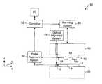
- a lithographic system 50includes a controller 52 , a scanning system 54 , an optical alignment system 56 , and a scanning probe alignment system 58 .
- Controller 52is configured to control the operation of scanning system 54 based upon position reference signals that are received from optical alignment system 56 and scanning probe alignment system 58 .
- Controller 52is not limited to any particular hardware, firmware or software configuration, but rather it may be implemented in any computing or processing environment.
- controller 52may be implemented in a high-level procedural or object oriented programming language, or in assembly or machine language; in any case, the programming language may be a compiled or interpreted language.
- Scanning system 54is configured to move a scanning head 60 precisely in a plane (i.e., the x-y plane) that is parallel to the support surface of stationary block 26 and to move scanning head 60 precisely in a direction (i.e., the z-direction) that is orthogonal to the support surface of stationary block 26 .
- Scanning head 60is configured to carry a mold 62 that includes a mold body 64 supporting a plurality of protruding features 66 and one or more scanning probes 68 .
- scanning head 60may be moved vertically by a z-axis scan actuator and may be moved horizontally by a separate x-y axis scan actuator.
- the z-axis scan actuator and the x-y axis scan actuatorboth may be carried on scanning head 60 .
- the z-axis scan actuator and the x-y axis scan actuatormay be implemented as planar electrostatic actuators (see, e.g., U.S. Pat. Nos. 6,136,208 and 5,801,472, which are incorporated herein by reference).
- Optical alignment system 56is configured to transmit position reference signals to controller 52 based upon light received from the surface of substrate 8 .
- optical alignment system 56may include a sensor that is configured to detect a moiré alignment pattern generated from suitably configured optical alignment marks carried on substrate 8 .
- conventional moiré alignment techniquesmay be used to move mold 62 into rough alignment with respect to the one or more optical alignment marks that are carried on substrate 8 .
- Other embodimentsmay employ different optical techniques (e.g., direct visual observation) to roughly align mold 62 with respect to the one or more optical alignment marks that are carried on substrate 8 .
- mold 62may be aligned to an atomic accuracy (e.g., on the order of 10 nm or less) based upon position reference signals received from scanning probe alignment system 58 .
- scanning probe alignment system 58may be implemented as a conventional scanning tunneling microscope (STM) scanning assembly, in which the positions of probes 68 are controlled based upon tunneling current information.
- scanning probe alignment system 58may be implemented as an atomic force microscope (AFM) scanning assembly, in which the positions of probes 68 are controlled based upon a force (e.g., an atomic force, an electrostatic force, or a magnetic force) that is generated between probes 68 and one or more scanning probe alignment marks 70 that are carried on substrate 8 .
- a forcee.g., an atomic force, an electrostatic force, or a magnetic force
- substrate 8may be lithographically processed as follows.
- a patterned bottom layer 74 and one or more scanning probe alignment marks 70are disposed on the substrate 8 (step 80 ).
- the bottom layer 74may be a wire layer consisting of a plurality of electrically conducting wires.
- the scanning probe alignment marks 70may be formed from electrically conducting material (e.g., aluminum or titanium) that is patterned to have one or more selected geometric shapes. Scanning probe alignment marks 70 may be coupled to scanning probe alignment system 58 by respective electrically conducting wires.
- a moldable thin film 6is disposed over the patterned bottom layer 74 , but not over the one or more alignment marks 70 (step 82 ; FIG. 4 ).
- the film 6includes a thermoplastic polymer (e.g., poly-methyl methacrylate (PMMA)).
- PMMApoly-methyl methacrylate
- a patterned mold 62is aligned optically with respect to the one or more optical alignment marks 76 (step 84 ; FIG. 4 ).
- the patterned mold 62may be aligned optically using a conventional moiré alignment technique. The patterned mold 62 then is aligned based upon interaction of one or more of the scanning probes 68 with one or more of the scanning probe alignment marks 70 .
- the scanning probe alignmentmay be based upon detection of a tunneling current between the scanning probes 68 and the alignment marks 70 or detection of a force (e.g., an atomic force, an electrostatic force, or a magnetic force) that is generated between the scanning probes 68 and the alignment marks 70 .
- a forcee.g., an atomic force, an electrostatic force, or a magnetic force
- the film 6may be heated to a temperature at which the film 6 is sufficiently softened relative to the hardness of the mold 62 so that the film 6 may conform to the protruding features 66 of the mold 62 .
- the film 6may be heated to a temperature that is at or above the glass transition temperature of the film 6 .
- the mold 62is removed from the film 6 (step 90 ; FIG. 4 ).
- the patterned film 6then may be further processed (step 92 ; FIG. 4 ).
- thinned regions 18 of the patterned film 6may be removed (e.g., by etching) to expose underlying regions 94 of the bottom layer (or the substrate).
- the resulting patterns in the film 6may be transferred (e.g., by lift-off processing) to a material 96 that is subsequently deposited onto substrate 8 .
- the resulting patterns in the film 6may be transferred (e.g., by etching) directly into substrate 8 .
- a pair of orthogonally-oriented alignment marks 98 , 100may be disposed on substrate 8 to enable controller 52 to precisely align mold 62 in the x-y plane, which is parallel to the exposed support surface of stationary block 26 .
- scanning probe alignment system 58may align mold 62 in the x-direction by detecting a leading edge 102 of alignment mark 98
- scanning probe alignment system 58may align mold 62 in the y-direction by detecting a leading edge 104 of alignment mark 100 .
- Mold 62also may be aligned based upon the detection of edges of alignment marks 98 , 100 that are different from edges 102 , 104 .
- other embodimentsmay include one, or more than two, alignment marks.
- the above-described imprinting lithographic processmay be used to fabricate a wide variety of different nano-scale devices.
- the above-described lithographic processmay be used to fabricate a molecular electronic device 110 that includes two electrically conducting wires 112 , 114 that are crossed at a non-zero angle, and a layer of bi-stable molecules or molecular compounds 116 (denoted by the symbol R) that is sandwiched between wires 112 , 114 .
- molecular electronic device 110may be fabricated as described in U.S. application Ser. No. 09/815,922, filed on Mar. 22, 2001, by Yong Chen, and entitled “Passivation Layer for Molecular Electronic Device Fabrication,” or as described in U.S. application Ser. No. 09/815,844, filed on Mar.
- electrically conducting wires 112 , 114may be patterned and aligned in accordance with the above-described imprint lithography process.
- Each wire 112 , 114may be formed from a metal or a doped semiconductor material.
- the particular molecule or molecules 18 (denoted by the symbol R s ) that are located at the intersection (or junction) of wires 112 , 114act as switch molecules and correspond to the active portion of molecular electronic device 110 .
- the state of molecular electronic device 110may be changed by applying a relatively high state-changing voltage across wires 112 , 114 .
- the magnitude of the state-changing voltageis sufficient to oxidize or reduce switch molecules 118 .
- Switch molecules 118may include a redox pair of molecular species that cooperate to balance charge such that when one of the molecular species is oxidized (or reduced), the other molecular species is reduced (or oxidized).
- one molecular speciesmay be reduced and the associated molecular species (the other half of the redox pair) may be oxidized.
- one molecular speciesmay be reduced and one of the wires 112 , 114 may be oxidized.
- one molecular speciesmay be oxidized and one of the wires 112 , 114 may be reduced.
- one wiremay be oxidized and an oxide associated with the other wire may be reduced.
- oxidation or reductionaffects the tunneling distance or the tunneling barrier height between the two wires, thereby exponentially altering the rate of charge transport across the wire junction.
- This electronic functionalityserves as the basis for operating molecular electronic device 10 as an electrical switch.
- molecular electronic device 110may be obtained from U.S. Pat. No. 6,128,214, which is incorporated herein by reference.
- molecular electronic device 110may exhibit any one of a variety of different electrical switching functions that may be used to controllably connect or disconnect bottom wire layer 112 and top wire layer 114 .
- the molecular electronic devicemay be singly configurable or reconfigurable.
- the initial state of molecular electronic device 110may be open or closed.
- the active material or molecules 118may be oxidized or reduced to permanently reverse the initial state of the device and, thereby, irreversibly close or open the switching state of the device.
- the switching devicemay be opened and closed multiple times by cycling the polarity and the magnitude of the applied voltage beyond appropriate threshold values that are selected to reversibly oxidize and reduce the active material or molecules 118 .
- bottom wire layer 112 and top wire layer 114depends upon the materials from which wire layers 112 , 114 and molecular layer 116 are formed.
- Table 1identifies the various types of electrical switching functions that may be obtained from different device material combinations.
- molecular electronic device 110may be incorporated into a resistive molecular wire crossbar memory 120 that includes a plurality of memory cells 122 that are arranged in multiple rows and multiple columns.
- Each memory cell 122includes a molecular electronic device 110 that is coupled between a respective bottom wire line 124 , 126 , 128 , 130 and a respective top wire line 132 , 134 , 136 , 138 .
- the voltage across a memory cellis determined by the voltages applied to the bottom wire line and the top wire line between which the memory cell is coupled.
- a control circuit 140is configured to address (or select), program information into, and read information from one or more memory cells 122 within memory cell array 120 .
- Molecular electronic devices 110are activated by electrochemical reduction or oxidation of the molecules 118 that are sandwiched between the bottom and top wire lines.
- the molecules of molecular layer 116are selected to have a large hysteresis in the voltammogram so that a switch may be oxidized at a relatively high voltage and its status may be read at a lower voltage.
- a switchis (electrochemically) closed, the resistance between connecting wires is low, which may correspond to a logic level of “1”.
- the switchis opened, the resistance is high, which may correspond to a logic level of “0”. Further details regarding the operation of a resistive molecular crossbar memory may be obtained from U.S. Pat. No. 6,128,214.
- molecular wire crossbar memory embodimentsmay include an array of molecular electronic devices that are configured to provide any one of the other switching functions identified in Table 1.
- the above-described molecular electronic devicesmay be implemented in a circuit designed to perform one or more logic (as opposed to memory) functions.
Landscapes
- Physics & Mathematics (AREA)
- General Physics & Mathematics (AREA)
- Engineering & Computer Science (AREA)
- Nanotechnology (AREA)
- Chemical & Material Sciences (AREA)
- Manufacturing & Machinery (AREA)
- Crystallography & Structural Chemistry (AREA)
- Condensed Matter Physics & Semiconductors (AREA)
- Theoretical Computer Science (AREA)
- Mathematical Physics (AREA)
- Computer Hardware Design (AREA)
- Microelectronics & Electronic Packaging (AREA)
- Power Engineering (AREA)
- Exposure Of Semiconductors, Excluding Electron Or Ion Beam Exposure (AREA)
Abstract
Description
| TABLE 1 | ||
| Wire Layer Materials | ||
| Semi- | |||||
| conductor- | |||||
| Metal- | Semi- | ||||
| Metal- | Metal- | Semi- | conductor | Semiconductor- | |
| Device | Metal | Metal | conduc- | (pn | Semiconductor |
| Type | (same) | (different) | tor | junction) | (heterojunction) |
| Resistor | X | X | X | ||
| Tunneling | X | X | X | ||
| Resistor | |||||
| Resonant | X | X | X | ||
| Tunneling | |||||
| Resistor | |||||
| Diode | X | X | X | X | |
| Tunneling | X | X | X | ||
| Diode | |||||
| Resonant | X | X | X | X | |
| Tunneling | |||||
| Diode | |||||
| Battery | X | X | X | ||
Claims (14)
Priority Applications (5)
| Application Number | Priority Date | Filing Date | Title |
|---|---|---|---|
| US09/815,913US6955767B2 (en) | 2001-03-22 | 2001-03-22 | Scanning probe based lithographic alignment |
| PCT/US2002/008935WO2002077716A2 (en) | 2001-03-22 | 2002-03-21 | Scanning probe based lithographic alignment |
| KR10-2003-7012276AKR20040021592A (en) | 2001-03-22 | 2002-03-21 | Scanning probe based lithographic alignment |
| EP02725318AEP1377881B1 (en) | 2001-03-22 | 2002-03-21 | Scanning probe based lithographic alignment |
| JP2002575710AJP2005512304A (en) | 2001-03-22 | 2002-03-21 | Scanning probe-based lithography alignment |
Applications Claiming Priority (1)
| Application Number | Priority Date | Filing Date | Title |
|---|---|---|---|
| US09/815,913US6955767B2 (en) | 2001-03-22 | 2001-03-22 | Scanning probe based lithographic alignment |
Publications (2)
| Publication Number | Publication Date |
|---|---|
| US20020170880A1 US20020170880A1 (en) | 2002-11-21 |
| US6955767B2true US6955767B2 (en) | 2005-10-18 |
Family
ID=25219166
Family Applications (1)
| Application Number | Title | Priority Date | Filing Date |
|---|---|---|---|
| US09/815,913Expired - LifetimeUS6955767B2 (en) | 2001-03-22 | 2001-03-22 | Scanning probe based lithographic alignment |
Country Status (5)
| Country | Link |
|---|---|
| US (1) | US6955767B2 (en) |
| EP (1) | EP1377881B1 (en) |
| JP (1) | JP2005512304A (en) |
| KR (1) | KR20040021592A (en) |
| WO (1) | WO2002077716A2 (en) |
Cited By (39)
| Publication number | Priority date | Publication date | Assignee | Title |
|---|---|---|---|---|
| US20050146078A1 (en)* | 2000-07-18 | 2005-07-07 | Stephen Chou | Apparatus for double-sided imprint lithography |
| US20050270312A1 (en)* | 2004-06-03 | 2005-12-08 | Molecular Imprints, Inc. | Fluid dispensing and drop-on-demand dispensing for nano-scale manufacturing |
| US20060077374A1 (en)* | 2002-07-11 | 2006-04-13 | Molecular Imprints, Inc. | Step and repeat imprint lithography systems |
| US20060157444A1 (en)* | 2004-12-09 | 2006-07-20 | Takashi Nakamura | Imprinting machine and device manufacturing method |
| US20060177532A1 (en)* | 2005-02-04 | 2006-08-10 | Molecular Imprints, Inc. | Imprint lithography method to control extrusion of a liquid from a desired region on a substrate |
| US20070064384A1 (en)* | 2005-08-25 | 2007-03-22 | Molecular Imprints, Inc. | Method to transfer a template transfer body between a motion stage and a docking plate |
| US20070074635A1 (en)* | 2005-08-25 | 2007-04-05 | Molecular Imprints, Inc. | System to couple a body and a docking plate |
| US20070117282A1 (en)* | 2003-01-23 | 2007-05-24 | Wataru Saito | Thin film transistor and method for manufacturing the same |
| US20070145004A1 (en)* | 2005-12-26 | 2007-06-28 | Jin Wuk Kim | Method for fabricating thin film pattern and method for fabricating flat panel display device using the same |
| US20070200276A1 (en)* | 2006-02-24 | 2007-08-30 | Micron Technology, Inc. | Method for rapid printing of near-field and imprint lithographic features |
| US20070228609A1 (en)* | 2006-04-03 | 2007-10-04 | Molecular Imprints, Inc. | Imprinting of Partial Fields at the Edge of the Wafer |
| US20070231981A1 (en)* | 2006-04-03 | 2007-10-04 | Molecular Imprints, Inc. | Patterning a Plurality of Fields on a Substrate to Compensate for Differing Evaporation Times |
| US20070248892A1 (en)* | 2004-07-14 | 2007-10-25 | Ivo Rangelow | A method of aligning a first article relative to a second article and an apparatus for aligning a first article relative to a second article |
| US20080067721A1 (en)* | 2006-09-14 | 2008-03-20 | Zhaoning Yu | Nanoimprint molds and methods of forming the same |
| US20080090312A1 (en)* | 2006-10-17 | 2008-04-17 | Inkyu Park | LITHOGRAPHY ALIGNMENT SYSTEM AND METHOD USING nDSE-BASED FEEDBACK CONTROL |
| US7547504B2 (en) | 2004-09-21 | 2009-06-16 | Molecular Imprints, Inc. | Pattern reversal employing thick residual layers |
| US7547398B2 (en) | 2006-04-18 | 2009-06-16 | Molecular Imprints, Inc. | Self-aligned process for fabricating imprint templates containing variously etched features |
| US7635263B2 (en) | 2005-01-31 | 2009-12-22 | Molecular Imprints, Inc. | Chucking system comprising an array of fluid chambers |
| US7636999B2 (en) | 2005-01-31 | 2009-12-29 | Molecular Imprints, Inc. | Method of retaining a substrate to a wafer chuck |
| US7665981B2 (en) | 2005-08-25 | 2010-02-23 | Molecular Imprints, Inc. | System to transfer a template transfer body between a motion stage and a docking plate |
| US7670530B2 (en) | 2006-01-20 | 2010-03-02 | Molecular Imprints, Inc. | Patterning substrates employing multiple chucks |
| US7670534B2 (en) | 2005-09-21 | 2010-03-02 | Molecular Imprints, Inc. | Method to control an atmosphere between a body and a substrate |
| US7670529B2 (en) | 2005-12-08 | 2010-03-02 | Molecular Imprints, Inc. | Method and system for double-sided patterning of substrates |
| US20100105206A1 (en)* | 2004-06-01 | 2010-04-29 | Semiconductor Energy Laboratory Co., Ltd. | Method for manufacturing semiconductor device |
| US7780893B2 (en) | 2006-04-03 | 2010-08-24 | Molecular Imprints, Inc. | Method of concurrently patterning a substrate having a plurality of fields and a plurality of alignment marks |
| US7785526B2 (en) | 2004-07-20 | 2010-08-31 | Molecular Imprints, Inc. | Imprint alignment method, system, and template |
| US7803308B2 (en) | 2005-12-01 | 2010-09-28 | Molecular Imprints, Inc. | Technique for separating a mold from solidified imprinting material |
| US7811505B2 (en) | 2004-12-07 | 2010-10-12 | Molecular Imprints, Inc. | Method for fast filling of templates for imprint lithography using on template dispense |
| US20100308485A1 (en)* | 2009-06-05 | 2010-12-09 | Ryoichi Inanami | Pattern forming apparatus and pattern forming method |
| US7854867B2 (en) | 2006-04-21 | 2010-12-21 | Molecular Imprints, Inc. | Method for detecting a particle in a nanoimprint lithography system |
| US7906058B2 (en) | 2005-12-01 | 2011-03-15 | Molecular Imprints, Inc. | Bifurcated contact printing technique |
| US7939131B2 (en) | 2004-08-16 | 2011-05-10 | Molecular Imprints, Inc. | Method to provide a layer with uniform etch characteristics |
| US8012395B2 (en) | 2006-04-18 | 2011-09-06 | Molecular Imprints, Inc. | Template having alignment marks formed of contrast material |
| CN102683181A (en)* | 2011-03-14 | 2012-09-19 | 上海华虹Nec电子有限公司 | Method for improving photoetching registration accuracy in germanium silicon technology |
| US8647554B2 (en) | 2004-06-15 | 2014-02-11 | Molecular Imprints, Inc. | Residual layer thickness measurement and correction |
| US8808808B2 (en) | 2005-07-22 | 2014-08-19 | Molecular Imprints, Inc. | Method for imprint lithography utilizing an adhesion primer layer |
| US20140291879A1 (en)* | 2005-12-21 | 2014-10-02 | Asml Netherlands B.V. | Imprint lithography |
| US8850980B2 (en) | 2006-04-03 | 2014-10-07 | Canon Nanotechnologies, Inc. | Tessellated patterns in imprint lithography |
| US9223202B2 (en) | 2000-07-17 | 2015-12-29 | Board Of Regents, The University Of Texas System | Method of automatic fluid dispensing for imprint lithography processes |
Families Citing this family (23)
| Publication number | Priority date | Publication date | Assignee | Title |
|---|---|---|---|---|
| AU2003230676A1 (en)* | 2002-03-15 | 2003-09-29 | Princeton University | Laser assisted direct imprint lithography |
| US7019819B2 (en)* | 2002-11-13 | 2006-03-28 | Molecular Imprints, Inc. | Chucking system for modulating shapes of substrates |
| US6787392B2 (en)* | 2002-09-09 | 2004-09-07 | Semiconductor Components Industries, L.L.C. | Structure and method of direct chip attach |
| FR2849221B1 (en)* | 2002-12-23 | 2005-10-07 | Commissariat Energie Atomique | METHOD FOR PRESSING LITHOGRAPHY OF A SUBSTRATE EMPLOYING A NANO-PRINTING |
| US7510946B2 (en) | 2003-03-17 | 2009-03-31 | Princeton University | Method for filling of nanoscale holes and trenches and for planarizing of a wafer surface |
| DE10311855B4 (en)* | 2003-03-17 | 2005-04-28 | Infineon Technologies Ag | Arrangement for transferring information / structures to wafers using a stamp |
| DE10330456B9 (en)* | 2003-07-05 | 2007-11-08 | Erich Thallner | Device for creating a surface structure on a wafer |
| US7654816B2 (en)* | 2004-10-07 | 2010-02-02 | Hewlett-Packard Development Company, L.P. | Lithographic mask alignment |
| EP1842228A4 (en)* | 2005-01-10 | 2010-03-10 | Bioforce Nanosciences Inc | System and method for creating a surface pattern |
| KR100647314B1 (en)* | 2005-01-31 | 2006-11-23 | 삼성전자주식회사 | Alignment system for nanoimprint lithography and imprint lithography method using the same |
| US20060267231A1 (en)* | 2005-05-27 | 2006-11-30 | Asml Netherlands B.V. | Imprint lithography |
| US9478501B2 (en) | 2006-03-08 | 2016-10-25 | Erich Thallner | Substrate processing and alignment |
| ATE409893T1 (en)* | 2006-03-08 | 2008-10-15 | Erich Thallner | METHOD FOR PRODUCING A COMPONENT AND APPARATUS FOR PROCESSING A SUBSTRATE, AND SUBSTRATE SUPPORT |
| JP4958614B2 (en)* | 2006-04-18 | 2012-06-20 | キヤノン株式会社 | Pattern transfer apparatus, imprint apparatus, pattern transfer method, and alignment apparatus |
| JP4795300B2 (en)* | 2006-04-18 | 2011-10-19 | キヤノン株式会社 | Alignment method, imprint method, alignment apparatus, imprint apparatus, and position measurement method |
| DE102006019962A1 (en)* | 2006-04-28 | 2007-11-08 | Infineon Technologies Ag | Imprint mask and method for aligning the imprint mask |
| KR101261606B1 (en) | 2006-05-09 | 2013-05-09 | 삼성디스플레이 주식회사 | Apparatus for manufacturing a display panel and method for manufacturing the same |
| KR100797093B1 (en)* | 2006-07-07 | 2008-01-22 | 한국기계연구원 | Nano device structure and manufacturing method thereof |
| US20080020303A1 (en)* | 2006-07-24 | 2008-01-24 | Wei Wu | Alignment for contact lithography |
| US20080090160A1 (en)* | 2006-10-13 | 2008-04-17 | Jason Blackstock | Alignment for contact lithography |
| KR20150095971A (en)* | 2014-02-12 | 2015-08-24 | 삼성디스플레이 주식회사 | Master mold, imprint mold and method of manufacturing display device using the imprint mold |
| JP6415120B2 (en)* | 2014-06-09 | 2018-10-31 | キヤノン株式会社 | Imprint apparatus and article manufacturing method |
| CN115826351B (en)* | 2022-07-26 | 2025-10-03 | 西湖微纳科技(杭州)有限公司 | Nanoimprinting device for scanning microprobe alignment and control method thereof |
Citations (10)
| Publication number | Priority date | Publication date | Assignee | Title |
|---|---|---|---|---|
| US5038322A (en) | 1988-09-21 | 1991-08-06 | U.S. Philips Corporation | Method of and device for sub-micron processing a surface |
| JPH04342112A (en) | 1991-05-17 | 1992-11-27 | Olympus Optical Co Ltd | X-ray lithographic apparatus |
| US5317141A (en) | 1992-08-14 | 1994-05-31 | National Semiconductor Corporation | Apparatus and method for high-accuracy alignment |
| US5535185A (en) | 1993-01-21 | 1996-07-09 | Canon Kabushiki Kaisha | Information recording/reproduction apparatus using probe |
| US5772905A (en) | 1995-11-15 | 1998-06-30 | Regents Of The University Of Minnesota | Nanoimprint lithography |
| US5801472A (en) | 1995-08-18 | 1998-09-01 | Hitchi, Ltd. | Micro-fabricated device with integrated electrostatic actuator |
| US5866806A (en)* | 1996-10-11 | 1999-02-02 | Kla-Tencor Corporation | System for locating a feature of a surface |
| US6136208A (en) | 1999-05-03 | 2000-10-24 | Industrial Technology Research Institute | Manufacturing method for planar microprobe including electrostatic actuator using sacrificial layer technology |
| US6165911A (en) | 1999-12-29 | 2000-12-26 | Calveley; Peter Braden | Method of patterning a metal layer |
| WO2002017383A2 (en) | 2000-08-21 | 2002-02-28 | Board Of Regents, The University Of Texas System | Flexure based translation stage |
- 2001
- 2001-03-22USUS09/815,913patent/US6955767B2/ennot_activeExpired - Lifetime
- 2002
- 2002-03-21KRKR10-2003-7012276Apatent/KR20040021592A/ennot_activeWithdrawn
- 2002-03-21JPJP2002575710Apatent/JP2005512304A/enactivePending
- 2002-03-21WOPCT/US2002/008935patent/WO2002077716A2/enactiveApplication Filing
- 2002-03-21EPEP02725318Apatent/EP1377881B1/ennot_activeExpired - Lifetime
Patent Citations (10)
| Publication number | Priority date | Publication date | Assignee | Title |
|---|---|---|---|---|
| US5038322A (en) | 1988-09-21 | 1991-08-06 | U.S. Philips Corporation | Method of and device for sub-micron processing a surface |
| JPH04342112A (en) | 1991-05-17 | 1992-11-27 | Olympus Optical Co Ltd | X-ray lithographic apparatus |
| US5317141A (en) | 1992-08-14 | 1994-05-31 | National Semiconductor Corporation | Apparatus and method for high-accuracy alignment |
| US5535185A (en) | 1993-01-21 | 1996-07-09 | Canon Kabushiki Kaisha | Information recording/reproduction apparatus using probe |
| US5801472A (en) | 1995-08-18 | 1998-09-01 | Hitchi, Ltd. | Micro-fabricated device with integrated electrostatic actuator |
| US5772905A (en) | 1995-11-15 | 1998-06-30 | Regents Of The University Of Minnesota | Nanoimprint lithography |
| US5866806A (en)* | 1996-10-11 | 1999-02-02 | Kla-Tencor Corporation | System for locating a feature of a surface |
| US6136208A (en) | 1999-05-03 | 2000-10-24 | Industrial Technology Research Institute | Manufacturing method for planar microprobe including electrostatic actuator using sacrificial layer technology |
| US6165911A (en) | 1999-12-29 | 2000-12-26 | Calveley; Peter Braden | Method of patterning a metal layer |
| WO2002017383A2 (en) | 2000-08-21 | 2002-02-28 | Board Of Regents, The University Of Texas System | Flexure based translation stage |
Non-Patent Citations (2)
| Title |
|---|
| D L White and O R Wood-"Novel Alignment System for Inprint Lithography"-J Vac Sci Technol B 18(6) Nov./Dec. 2000-pp. 3552-3556. |
| Stephen Y. Chou et al., "Imprint Lithography with 25-Nanometer Resolution," Science, vol. 272 (Apr. 5, 1996). |
Cited By (55)
| Publication number | Priority date | Publication date | Assignee | Title |
|---|---|---|---|---|
| US9223202B2 (en) | 2000-07-17 | 2015-12-29 | Board Of Regents, The University Of Texas System | Method of automatic fluid dispensing for imprint lithography processes |
| US20050146078A1 (en)* | 2000-07-18 | 2005-07-07 | Stephen Chou | Apparatus for double-sided imprint lithography |
| US7717696B2 (en)* | 2000-07-18 | 2010-05-18 | Nanonex Corp. | Apparatus for double-sided imprint lithography |
| US20060077374A1 (en)* | 2002-07-11 | 2006-04-13 | Molecular Imprints, Inc. | Step and repeat imprint lithography systems |
| US7445971B2 (en)* | 2003-01-23 | 2008-11-04 | Dai Nippon Printing Co., Ltd. | Thin film transistor and method for manufacturing the same |
| US20070117282A1 (en)* | 2003-01-23 | 2007-05-24 | Wataru Saito | Thin film transistor and method for manufacturing the same |
| US8563438B2 (en)* | 2004-06-01 | 2013-10-22 | Semiconductor Energy Laboratory Co., Ltd. | Method for manufacturing semiconductor device |
| US20100105206A1 (en)* | 2004-06-01 | 2010-04-29 | Semiconductor Energy Laboratory Co., Ltd. | Method for manufacturing semiconductor device |
| US20050270312A1 (en)* | 2004-06-03 | 2005-12-08 | Molecular Imprints, Inc. | Fluid dispensing and drop-on-demand dispensing for nano-scale manufacturing |
| US8647554B2 (en) | 2004-06-15 | 2014-02-11 | Molecular Imprints, Inc. | Residual layer thickness measurement and correction |
| US20070248892A1 (en)* | 2004-07-14 | 2007-10-25 | Ivo Rangelow | A method of aligning a first article relative to a second article and an apparatus for aligning a first article relative to a second article |
| US7946029B2 (en) | 2004-07-14 | 2011-05-24 | Universitat Kassel | Apparatus for aligning a first article relative to a second article |
| US20110219635A1 (en)* | 2004-07-14 | 2011-09-15 | Universitat Kassel | Method of aligning a first article relative to a second article and an apparatus for aligning a first article relative to a second article |
| US10025207B2 (en) | 2004-07-14 | 2018-07-17 | Universität Kassel | Method of aligning a first article relative to a second article |
| US7785526B2 (en) | 2004-07-20 | 2010-08-31 | Molecular Imprints, Inc. | Imprint alignment method, system, and template |
| US8366434B2 (en)* | 2004-07-20 | 2013-02-05 | Molecular Imprints, Inc. | Imprint alignment method, system and template |
| US7939131B2 (en) | 2004-08-16 | 2011-05-10 | Molecular Imprints, Inc. | Method to provide a layer with uniform etch characteristics |
| US7547504B2 (en) | 2004-09-21 | 2009-06-16 | Molecular Imprints, Inc. | Pattern reversal employing thick residual layers |
| US7811505B2 (en) | 2004-12-07 | 2010-10-12 | Molecular Imprints, Inc. | Method for fast filling of templates for imprint lithography using on template dispense |
| US20100148397A1 (en)* | 2004-12-09 | 2010-06-17 | Canon Kabushiki Kaisha | Imprinting machine and device manufacturing method |
| US20060157444A1 (en)* | 2004-12-09 | 2006-07-20 | Takashi Nakamura | Imprinting machine and device manufacturing method |
| US7815424B2 (en)* | 2004-12-09 | 2010-10-19 | Canon Kabushiki Kaisha | Imprinting machine and device manufacturing method |
| US8834144B2 (en) | 2004-12-09 | 2014-09-16 | Canon Kabushiki Kaisha | Imprinting machine and device manufacturing method |
| US7635263B2 (en) | 2005-01-31 | 2009-12-22 | Molecular Imprints, Inc. | Chucking system comprising an array of fluid chambers |
| US7636999B2 (en) | 2005-01-31 | 2009-12-29 | Molecular Imprints, Inc. | Method of retaining a substrate to a wafer chuck |
| US20060177532A1 (en)* | 2005-02-04 | 2006-08-10 | Molecular Imprints, Inc. | Imprint lithography method to control extrusion of a liquid from a desired region on a substrate |
| US8808808B2 (en) | 2005-07-22 | 2014-08-19 | Molecular Imprints, Inc. | Method for imprint lithography utilizing an adhesion primer layer |
| US7665981B2 (en) | 2005-08-25 | 2010-02-23 | Molecular Imprints, Inc. | System to transfer a template transfer body between a motion stage and a docking plate |
| US20070064384A1 (en)* | 2005-08-25 | 2007-03-22 | Molecular Imprints, Inc. | Method to transfer a template transfer body between a motion stage and a docking plate |
| US20070074635A1 (en)* | 2005-08-25 | 2007-04-05 | Molecular Imprints, Inc. | System to couple a body and a docking plate |
| US7670534B2 (en) | 2005-09-21 | 2010-03-02 | Molecular Imprints, Inc. | Method to control an atmosphere between a body and a substrate |
| US7803308B2 (en) | 2005-12-01 | 2010-09-28 | Molecular Imprints, Inc. | Technique for separating a mold from solidified imprinting material |
| US7906058B2 (en) | 2005-12-01 | 2011-03-15 | Molecular Imprints, Inc. | Bifurcated contact printing technique |
| US7670529B2 (en) | 2005-12-08 | 2010-03-02 | Molecular Imprints, Inc. | Method and system for double-sided patterning of substrates |
| US9610727B2 (en)* | 2005-12-21 | 2017-04-04 | Asml Netherlands B.V. | Imprint lithography |
| US20140291879A1 (en)* | 2005-12-21 | 2014-10-02 | Asml Netherlands B.V. | Imprint lithography |
| US7544069B2 (en)* | 2005-12-26 | 2009-06-09 | Lg Display Co., Ltd. | Method for fabricating thin film pattern and method for fabricating flat panel display device using the same |
| US20070145004A1 (en)* | 2005-12-26 | 2007-06-28 | Jin Wuk Kim | Method for fabricating thin film pattern and method for fabricating flat panel display device using the same |
| US7670530B2 (en) | 2006-01-20 | 2010-03-02 | Molecular Imprints, Inc. | Patterning substrates employing multiple chucks |
| US20070200276A1 (en)* | 2006-02-24 | 2007-08-30 | Micron Technology, Inc. | Method for rapid printing of near-field and imprint lithographic features |
| US7780893B2 (en) | 2006-04-03 | 2010-08-24 | Molecular Imprints, Inc. | Method of concurrently patterning a substrate having a plurality of fields and a plurality of alignment marks |
| US20070231981A1 (en)* | 2006-04-03 | 2007-10-04 | Molecular Imprints, Inc. | Patterning a Plurality of Fields on a Substrate to Compensate for Differing Evaporation Times |
| US20070228609A1 (en)* | 2006-04-03 | 2007-10-04 | Molecular Imprints, Inc. | Imprinting of Partial Fields at the Edge of the Wafer |
| US8850980B2 (en) | 2006-04-03 | 2014-10-07 | Canon Nanotechnologies, Inc. | Tessellated patterns in imprint lithography |
| US8142850B2 (en) | 2006-04-03 | 2012-03-27 | Molecular Imprints, Inc. | Patterning a plurality of fields on a substrate to compensate for differing evaporation times |
| US7802978B2 (en) | 2006-04-03 | 2010-09-28 | Molecular Imprints, Inc. | Imprinting of partial fields at the edge of the wafer |
| US8012395B2 (en) | 2006-04-18 | 2011-09-06 | Molecular Imprints, Inc. | Template having alignment marks formed of contrast material |
| US7547398B2 (en) | 2006-04-18 | 2009-06-16 | Molecular Imprints, Inc. | Self-aligned process for fabricating imprint templates containing variously etched features |
| US7854867B2 (en) | 2006-04-21 | 2010-12-21 | Molecular Imprints, Inc. | Method for detecting a particle in a nanoimprint lithography system |
| US7780431B2 (en) | 2006-09-14 | 2010-08-24 | Hewlett-Packard Development Company, L.P. | Nanoimprint molds and methods of forming the same |
| US20080067721A1 (en)* | 2006-09-14 | 2008-03-20 | Zhaoning Yu | Nanoimprint molds and methods of forming the same |
| US20080090312A1 (en)* | 2006-10-17 | 2008-04-17 | Inkyu Park | LITHOGRAPHY ALIGNMENT SYSTEM AND METHOD USING nDSE-BASED FEEDBACK CONTROL |
| US20100308485A1 (en)* | 2009-06-05 | 2010-12-09 | Ryoichi Inanami | Pattern forming apparatus and pattern forming method |
| CN102683181B (en)* | 2011-03-14 | 2014-10-08 | 上海华虹宏力半导体制造有限公司 | Method for improving photoetching registration accuracy in germanium silicon technology |
| CN102683181A (en)* | 2011-03-14 | 2012-09-19 | 上海华虹Nec电子有限公司 | Method for improving photoetching registration accuracy in germanium silicon technology |
Also Published As
| Publication number | Publication date |
|---|---|
| EP1377881A2 (en) | 2004-01-07 |
| WO2002077716A2 (en) | 2002-10-03 |
| KR20040021592A (en) | 2004-03-10 |
| US20020170880A1 (en) | 2002-11-21 |
| EP1377881B1 (en) | 2012-12-05 |
| WO2002077716A3 (en) | 2003-11-06 |
| JP2005512304A (en) | 2005-04-28 |
Similar Documents
| Publication | Publication Date | Title |
|---|---|---|
| US6955767B2 (en) | Scanning probe based lithographic alignment | |
| US7654816B2 (en) | Lithographic mask alignment | |
| US10025207B2 (en) | Method of aligning a first article relative to a second article | |
| US7455788B2 (en) | Nanoscale electric lithography | |
| US5227626A (en) | Lithography apparatus using scanning tunneling microscopy | |
| US7175961B2 (en) | Photopatternable molecular circuitry | |
| Cerrina et al. | A path to nanolithography | |
| US6756296B2 (en) | Method for lithographic processing on molecular monolayer and multilayer thin films | |
| US7671616B2 (en) | Semiconductor probe having embossed resistive tip and method of fabricating the same | |
| JPH06204118A (en) | Substrate position alignment method | |
| KR100500390B1 (en) | Nano lithography system and method using parallel probe | |
| EP1740933A2 (en) | Apparatus and method for transverse characterization of materials | |
| KR100498988B1 (en) | Method of patterning by parallel probes | |
| Resnick et al. | Hybrid CMOS/Nanodevice Integrated Circuits Design and Fabrication |
Legal Events
| Date | Code | Title | Description |
|---|---|---|---|
| AS | Assignment | Owner name:HEWLETT-PACKARD COMPANY, COLORADO Free format text:ASSIGNMENT OF ASSIGNORS INTEREST;ASSIGNOR:CHEN, YONG;REEL/FRAME:012060/0479 Effective date:20010731 | |
| AS | Assignment | Owner name:HEWLETT-PACKARD DEVELOPMENT COMPANY L.P., TEXAS Free format text:ASSIGNMENT OF ASSIGNORS INTEREST;ASSIGNOR:HEWLETT-PACKARD COMPANY;REEL/FRAME:014061/0492 Effective date:20030926 Owner name:HEWLETT-PACKARD DEVELOPMENT COMPANY L.P.,TEXAS Free format text:ASSIGNMENT OF ASSIGNORS INTEREST;ASSIGNOR:HEWLETT-PACKARD COMPANY;REEL/FRAME:014061/0492 Effective date:20030926 | |
| STCF | Information on status: patent grant | Free format text:PATENTED CASE | |
| FPAY | Fee payment | Year of fee payment:4 | |
| AS | Assignment | Owner name:SAMSUNG ELECTRONICS CO., LTD., KOREA, REPUBLIC OF Free format text:ASSIGNMENT OF ASSIGNORS INTEREST;ASSIGNORS:HEWLETT-PACKARD DEVELOPMENT COMPANY, L.P.;HEWLETT-PACKARD COMPANY;REEL/FRAME:026198/0139 Effective date:20101019 | |
| FEPP | Fee payment procedure | Free format text:PAYOR NUMBER ASSIGNED (ORIGINAL EVENT CODE: ASPN); ENTITY STATUS OF PATENT OWNER: LARGE ENTITY | |
| FPAY | Fee payment | Year of fee payment:8 | |
| FPAY | Fee payment | Year of fee payment:12 |