US6954256B2 - Gradient immersion lithography - Google Patents
Gradient immersion lithographyDownload PDFInfo
- Publication number
- US6954256B2 US6954256B2US10/698,012US69801203AUS6954256B2US 6954256 B2US6954256 B2US 6954256B2US 69801203 AUS69801203 AUS 69801203AUS 6954256 B2US6954256 B2US 6954256B2
- Authority
- US
- United States
- Prior art keywords
- refraction
- index
- fluid
- substrate
- radiation
- Prior art date
- Legal status (The legal status is an assumption and is not a legal conclusion. Google has not performed a legal analysis and makes no representation as to the accuracy of the status listed.)
- Expired - Fee Related
Links
- 238000000671immersion lithographyMethods0.000titledescription2
- 239000012530fluidSubstances0.000claimsabstractdescription134
- 239000000758substrateSubstances0.000claimsabstractdescription79
- 230000003287optical effectEffects0.000claimsabstractdescription51
- 238000004519manufacturing processMethods0.000claimsabstractdescription24
- 230000005855radiationEffects0.000claimsdescription57
- 239000010702perfluoropolyetherSubstances0.000claimsdescription20
- 238000000059patterningMethods0.000claimsdescription13
- 239000000463materialSubstances0.000claimsdescription10
- XLYOFNOQVPJJNP-UHFFFAOYSA-NwaterSubstancesOXLYOFNOQVPJJNP-UHFFFAOYSA-N0.000claimsdescription8
- 239000007789gasSubstances0.000description23
- 239000010410layerSubstances0.000description15
- 238000000034methodMethods0.000description15
- 238000001459lithographyMethods0.000description5
- VYPSYNLAJGMNEJ-UHFFFAOYSA-Nsilicon dioxideInorganic materialsO=[Si]=OVYPSYNLAJGMNEJ-UHFFFAOYSA-N0.000description5
- WUKWITHWXAAZEY-UHFFFAOYSA-Lcalcium difluorideChemical compound[F-].[F-].[Ca+2]WUKWITHWXAAZEY-UHFFFAOYSA-L0.000description4
- 229910001634calcium fluorideInorganic materials0.000description4
- 238000013461designMethods0.000description4
- 238000009826distributionMethods0.000description4
- 238000005530etchingMethods0.000description4
- 239000007788liquidSubstances0.000description4
- 239000011159matrix materialSubstances0.000description4
- 230000008569processEffects0.000description4
- 238000012545processingMethods0.000description4
- QVGXLLKOCUKJST-UHFFFAOYSA-Natomic oxygenChemical compound[O]QVGXLLKOCUKJST-UHFFFAOYSA-N0.000description3
- 230000001419dependent effectEffects0.000description3
- 238000010894electron beam technologyMethods0.000description3
- 239000005350fused silica glassSubstances0.000description3
- 238000003384imaging methodMethods0.000description3
- 229910052760oxygenInorganic materials0.000description3
- 239000001301oxygenSubstances0.000description3
- 239000000126substanceSubstances0.000description3
- XUIMIQQOPSSXEZ-UHFFFAOYSA-NSiliconChemical compound[Si]XUIMIQQOPSSXEZ-UHFFFAOYSA-N0.000description2
- 238000003491arrayMethods0.000description2
- 230000003247decreasing effectEffects0.000description2
- 230000000694effectsEffects0.000description2
- 229920001971elastomerPolymers0.000description2
- 230000006870functionEffects0.000description2
- 238000007689inspectionMethods0.000description2
- 238000010884ion-beam techniqueMethods0.000description2
- 230000010363phase shiftEffects0.000description2
- 239000004065semiconductorSubstances0.000description2
- 239000010703siliconSubstances0.000description2
- 229910052710siliconInorganic materials0.000description2
- 239000002841Lewis acidSubstances0.000description1
- CBENFWSGALASAD-UHFFFAOYSA-NOzoneChemical compound[O-][O+]=OCBENFWSGALASAD-UHFFFAOYSA-N0.000description1
- NINIDFKCEFEMDL-UHFFFAOYSA-NSulfurChemical compound[S]NINIDFKCEFEMDL-UHFFFAOYSA-N0.000description1
- 238000002835absorbanceMethods0.000description1
- 239000002253acidSubstances0.000description1
- 150000007513acidsChemical class0.000description1
- 230000009471actionEffects0.000description1
- 229910052782aluminiumInorganic materials0.000description1
- XAGFODPZIPBFFR-UHFFFAOYSA-NaluminiumChemical compound[Al]XAGFODPZIPBFFR-UHFFFAOYSA-N0.000description1
- 230000002238attenuated effectEffects0.000description1
- 230000008901benefitEffects0.000description1
- 230000005540biological transmissionEffects0.000description1
- 230000008859changeEffects0.000description1
- 239000003795chemical substances by applicationSubstances0.000description1
- 239000011248coating agentSubstances0.000description1
- 238000000576coating methodMethods0.000description1
- 238000010276constructionMethods0.000description1
- 238000012937correctionMethods0.000description1
- 238000001514detection methodMethods0.000description1
- 238000011161developmentMethods0.000description1
- 230000009977dual effectEffects0.000description1
- 239000000806elastomerSubstances0.000description1
- 230000005684electric fieldEffects0.000description1
- 230000005670electromagnetic radiationEffects0.000description1
- 230000007613environmental effectEffects0.000description1
- 230000008020evaporationEffects0.000description1
- 238000001704evaporationMethods0.000description1
- 239000010408filmSubstances0.000description1
- 239000000499gelSubstances0.000description1
- 239000011521glassSubstances0.000description1
- 238000005286illuminationMethods0.000description1
- 238000007654immersionMethods0.000description1
- 238000009413insulationMethods0.000description1
- 230000010354integrationEffects0.000description1
- 238000005468ion implantationMethods0.000description1
- 230000005865ionizing radiationEffects0.000description1
- 150000002500ionsChemical class0.000description1
- 239000002346layers by functionSubstances0.000description1
- 150000007517lewis acidsChemical class0.000description1
- 239000004973liquid crystal related substanceSubstances0.000description1
- 239000000314lubricantSubstances0.000description1
- 230000005381magnetic domainEffects0.000description1
- 238000005259measurementMethods0.000description1
- 230000015654memoryEffects0.000description1
- QSHDDOUJBYECFT-UHFFFAOYSA-NmercuryChemical compound[Hg]QSHDDOUJBYECFT-UHFFFAOYSA-N0.000description1
- 229910052753mercuryInorganic materials0.000description1
- 229910052751metalInorganic materials0.000description1
- 239000002184metalSubstances0.000description1
- 238000001465metallisationMethods0.000description1
- 231100000252nontoxicToxicity0.000description1
- 230000003000nontoxic effectEffects0.000description1
- 239000007800oxidant agentSubstances0.000description1
- 230000003647oxidationEffects0.000description1
- 238000007254oxidation reactionMethods0.000description1
- 230000001590oxidative effectEffects0.000description1
- 238000004806packaging method and processMethods0.000description1
- 239000002245particleSubstances0.000description1
- 239000004033plasticSubstances0.000description1
- 229920003023plasticPolymers0.000description1
- 238000005498polishingMethods0.000description1
- 238000006116polymerization reactionMethods0.000description1
- 230000037452primingEffects0.000description1
- 238000007639printingMethods0.000description1
- 239000010453quartzSubstances0.000description1
- 239000005060rubberSubstances0.000description1
- 238000007789sealingMethods0.000description1
- 238000007493shaping processMethods0.000description1
- 239000002904solventSubstances0.000description1
- 238000003860storageMethods0.000description1
- 229910052717sulfurInorganic materials0.000description1
- 239000011593sulfurSubstances0.000description1
- 238000012360testing methodMethods0.000description1
- 239000010409thin filmSubstances0.000description1
- 238000001771vacuum depositionMethods0.000description1
Images


Classifications
- G—PHYSICS
- G03—PHOTOGRAPHY; CINEMATOGRAPHY; ANALOGOUS TECHNIQUES USING WAVES OTHER THAN OPTICAL WAVES; ELECTROGRAPHY; HOLOGRAPHY
- G03F—PHOTOMECHANICAL PRODUCTION OF TEXTURED OR PATTERNED SURFACES, e.g. FOR PRINTING, FOR PROCESSING OF SEMICONDUCTOR DEVICES; MATERIALS THEREFOR; ORIGINALS THEREFOR; APPARATUS SPECIALLY ADAPTED THEREFOR
- G03F7/00—Photomechanical, e.g. photolithographic, production of textured or patterned surfaces, e.g. printing surfaces; Materials therefor, e.g. comprising photoresists; Apparatus specially adapted therefor
- G03F7/70—Microphotolithographic exposure; Apparatus therefor
- G03F7/708—Construction of apparatus, e.g. environment aspects, hygiene aspects or materials
- G03F7/7095—Materials, e.g. materials for housing, stage or other support having particular properties, e.g. weight, strength, conductivity, thermal expansion coefficient
- G03F7/70958—Optical materials or coatings, e.g. with particular transmittance, reflectance or anti-reflection properties
- G03F7/70966—Birefringence
- G—PHYSICS
- G03—PHOTOGRAPHY; CINEMATOGRAPHY; ANALOGOUS TECHNIQUES USING WAVES OTHER THAN OPTICAL WAVES; ELECTROGRAPHY; HOLOGRAPHY
- G03F—PHOTOMECHANICAL PRODUCTION OF TEXTURED OR PATTERNED SURFACES, e.g. FOR PRINTING, FOR PROCESSING OF SEMICONDUCTOR DEVICES; MATERIALS THEREFOR; ORIGINALS THEREFOR; APPARATUS SPECIALLY ADAPTED THEREFOR
- G03F7/00—Photomechanical, e.g. photolithographic, production of textured or patterned surfaces, e.g. printing surfaces; Materials therefor, e.g. comprising photoresists; Apparatus specially adapted therefor
- G03F7/70—Microphotolithographic exposure; Apparatus therefor
- G03F7/70216—Mask projection systems
- G03F7/70341—Details of immersion lithography aspects, e.g. exposure media or control of immersion liquid supply
- G—PHYSICS
- G03—PHOTOGRAPHY; CINEMATOGRAPHY; ANALOGOUS TECHNIQUES USING WAVES OTHER THAN OPTICAL WAVES; ELECTROGRAPHY; HOLOGRAPHY
- G03F—PHOTOMECHANICAL PRODUCTION OF TEXTURED OR PATTERNED SURFACES, e.g. FOR PRINTING, FOR PROCESSING OF SEMICONDUCTOR DEVICES; MATERIALS THEREFOR; ORIGINALS THEREFOR; APPARATUS SPECIALLY ADAPTED THEREFOR
- G03F7/00—Photomechanical, e.g. photolithographic, production of textured or patterned surfaces, e.g. printing surfaces; Materials therefor, e.g. comprising photoresists; Apparatus specially adapted therefor
- G03F7/70—Microphotolithographic exposure; Apparatus therefor
- G03F7/708—Construction of apparatus, e.g. environment aspects, hygiene aspects or materials
- G03F7/7095—Materials, e.g. materials for housing, stage or other support having particular properties, e.g. weight, strength, conductivity, thermal expansion coefficient
- G03F7/70958—Optical materials or coatings, e.g. with particular transmittance, reflectance or anti-reflection properties
- G—PHYSICS
- G03—PHOTOGRAPHY; CINEMATOGRAPHY; ANALOGOUS TECHNIQUES USING WAVES OTHER THAN OPTICAL WAVES; ELECTROGRAPHY; HOLOGRAPHY
- G03F—PHOTOMECHANICAL PRODUCTION OF TEXTURED OR PATTERNED SURFACES, e.g. FOR PRINTING, FOR PROCESSING OF SEMICONDUCTOR DEVICES; MATERIALS THEREFOR; ORIGINALS THEREFOR; APPARATUS SPECIALLY ADAPTED THEREFOR
- G03F7/00—Photomechanical, e.g. photolithographic, production of textured or patterned surfaces, e.g. printing surfaces; Materials therefor, e.g. comprising photoresists; Apparatus specially adapted therefor
- G03F7/70—Microphotolithographic exposure; Apparatus therefor
- G03F7/708—Construction of apparatus, e.g. environment aspects, hygiene aspects or materials
- G03F7/70983—Optical system protection, e.g. pellicles or removable covers for protection of mask
- Y—GENERAL TAGGING OF NEW TECHNOLOGICAL DEVELOPMENTS; GENERAL TAGGING OF CROSS-SECTIONAL TECHNOLOGIES SPANNING OVER SEVERAL SECTIONS OF THE IPC; TECHNICAL SUBJECTS COVERED BY FORMER USPC CROSS-REFERENCE ART COLLECTIONS [XRACs] AND DIGESTS
- Y10—TECHNICAL SUBJECTS COVERED BY FORMER USPC
- Y10S—TECHNICAL SUBJECTS COVERED BY FORMER USPC CROSS-REFERENCE ART COLLECTIONS [XRACs] AND DIGESTS
- Y10S430/00—Radiation imagery chemistry: process, composition, or product thereof
- Y10S430/162—Protective or antiabrasion layer
Definitions
- the present inventionrelates to a lithographic apparatus, in particular to a lithographic apparatus in which the space between an optical element of a projection system and a substrate is filled with at least two fluids having different indices of refraction.
- the present inventionalso relates to a device manufacturing method.
- patterning deviceas here employed should be broadly interpreted as referring to device that can be used to endow an incoming radiation beam with a patterned cross-section, corresponding to a pattern that is to be created in a target portion of the substrate.
- the term “light valve”can also be used in this context.
- the patternwill correspond to a particular functional layer in a device being created in the target portion, such as an integrated circuit or other device.
- An example of such a patterning deviceis a mask.
- the concept of a maskis well known in lithography, and it includes mask types such as binary, alternating phase shift, and attenuated phase shift, as well as various hybrid mask types.
- Placement of such a mask in the radiation beamcauses selective transmission (in the case of a transmissive mask) or reflection (in the case of a reflective mask) of the radiation impinging on the mask, according to the pattern on the mask.
- the supportwill generally be a mask table, which ensures that the mask can be held at a desired position in the incoming radiation beam, and that it can be moved relative to the beam if so desired.
- a patterning deviceis a programmable mirror array.
- One example of such an arrayis a matrix-addressable surface having a viscoelastic control layer and a reflective surface.
- the basic principle behind such an apparatusis that, for example, addressed areas of the reflective surface reflect incident light as diffracted light, whereas unaddressed areas reflect incident light as undiffracted light.
- the undiffracted lightcan be filtered out of the reflected beam, leaving only the diffracted light behind. In this manner, the beam becomes patterned according to the addressing pattern of the matrix addressable surface.
- An alternative embodiment of a programmable mirror arrayemploys a matrix arrangement of tiny mirrors, each of which can be individually tilted about an axis by applying a suitable localized electric field, or by employing piezoelectric actuators.
- the mirrorsare matrix addressable, such that addressed mirrors will reflect an incoming radiation beam in a different direction to unaddressed mirrors.
- the reflected beamis patterned according to the addressing pattern of the matrix-addressable mirrors.
- the required matrix addressingcan be performed using suitable electronics.
- the patterning devicecan comprise one or more programmable mirror arrays. More information on mirror arrays as here referred to can be seen, for example, from U.S. Pat. Nos.
- the support structuremay be embodied as a frame or table, for example, which may be fixed or movable as required.
- a patterning deviceis a programmable LCD array.
- a programmable LCD arrayAn example of such a construction is given in U.S. Pat. No. 5,229,872.
- the support structure in this casemay be embodied as a frame or table, for example, which may be fixed or movable as required.
- Lithographic projection apparatuscan be used, for example, in the manufacture of integrated circuits (ICs).
- the patterning devicemay generate a circuit pattern corresponding to an individual layer of the IC, and this pattern can be imaged onto a target portion (e.g. comprising one or more dies) on a substrate (silicon wafer) that has been coated with a layer of radiation sensitive material (resist).
- a target portione.g. comprising one or more dies
- a substratesilicon wafer
- a layer of radiation sensitive materialresist
- a single waferwill contain a whole network of adjacent target portions that are successively irradiated via the projection system, one at a time.
- employing patterning by a mask on a mask tablea distinction can be made between two different types of machine.
- each target portionis irradiated by exposing the entire mask pattern onto the target portion at once.
- Such an apparatusis commonly referred to as a wafer stepper.
- each target portionis irradiated by progressively scanning the mask pattern under the beam of radiation in a given reference direction (the “scanning” direction) while synchronously scanning the substrate table parallel or anti-parallel to this direction.
- the projection systemwill have a magnification factor M (generally ⁇ 1)
- Mmagnification factor
- the speed V at which the substrate table is scannedwill be a factor M times that at which the mask table is scanned. More information with regard to lithographic devices as here described can be seen, for example, from U.S. Pat. No. 6,046,792.
- a pattern(e.g. in a mask) is imaged onto a substrate that is at least partially covered by a layer of radiation sensitive material (resist).
- the substratePrior to this imaging, the substrate may undergo various procedures, such as priming, resist coating and a soft bake. After exposure, the substrate may be subjected to other procedures, such as a post-exposure bake (PEB), development, a hard bake and measurement and/or inspection of the imaged features.
- PEBpost-exposure bake
- This array of proceduresis used as a basis to pattern an individual layer of a device, e.g. an IC.
- Such a patterned layermay then undergo various processes such as etching, ion-implantation (doping), metallization, oxidation, chemical, mechanical polishing, etc., all intended to finish off an individual layer. If several layers are required, then the whole procedure, or a variant thereof, will have to be repeated for each new layer. It is important to ensure that the overlay (juxtaposition) of the various stacked layers is as accurate as possible. For this purpose, a small reference mark is provided at one or more positions on the wafer, thus defining the origin of a coordinate system on the wafer.
- this markcan then be relocated each time a new layer has to be juxtaposed on an existing layer, and can be used as an alignment reference.
- an array of deviceswill be present on the substrate (wafer). These devices are then separated from one another by a technique such as dicing or sawing, whence the individual devices can be mounted on a carrier, connected to pins, etc. Further information regarding such processes can be obtained, for example, from the book “Microchip Fabrication: A Practical Guide to Semiconductor Processing”, Third Edition, by Peter van Zant, McGraw Hill Publishing Co., 1997, ISBN 0-07-067250-4.
- the projection systemmay hereinafter be referred to as the “lens.”
- the radiation systemmay also include components operating according to any of these design types for directing, shaping or controlling the projection beam of radiation, and such components may also be referred to below, collectively or singularly, as a “lens.”
- the lithographic apparatusmay be of a type having two or more substrate tables (and/or two or more mask tables). In such “multiple stage” devices the additional tables may be used in parallel or preparatory steps may be carried out on one or more tables while one or more other tables are being used for exposures. Dual stage lithographic apparatus are described, for example, in U.S. Pat. Nos. 5,969,441 and 6,262,796.
- a lower limit of k 1is 0.25 and lithographic projection apparatus having a NA of 0.85 are currently available. Difficulties in optical design make increasing the NA difficult. As k 1 and NA are generally considered to be at their limits, the ability to decrease the resolution, i.e, print smaller pattern features, of lithographic projection apparatus appears to be dependent on decreasing the wavelength ⁇ of the radiation.
- One method of decreasing the wavelength of the radiationis to immerse the substrate in a lithographic projection apparatus in a fluid having a relatively high refractive index, e.g., water, so as to fill the space between the optical element of the projection system (lens) and the substrate. Filling the space between the optical element of the projection system and the substrate enables the imaging of smaller features as the exposure radiation has a shorter wavelength in the fluid.
- the effect of the fluidmay be regarded as increasing the effective NA of the system.
- This methodcan also be used to increase the depth of focus for imaging at the same resolution.
- the fluidhas an index of refraction between the indices of refraction of the optical element and the substrate.
- the index of refraction of the fluidmay not be sufficient to improve the resolution of the image.
- the fluidis only able to provide a single decrease in the wavelength of the radiation as the index of refraction of the fluid is constant throughout the space between the optical element and the substrate.
- the term fluidrefers to liquids, gases, and/or gels.
- a lithographic apparatusincluding a radiation system constructed and arranged to supply a beam of radiation; a support constructed and arranged to support a patterning device, the patterning device constructed and arranged to pattern the beam of radiation according to a desired pattern; a substrate table to hold a substrate; a projection system constructed and arranged to project the patterned beam onto a target portion of the substrate; a transparent plate positioned between an optical element of the projection system and the substrate; a first fluid having a first index of refraction filling a first space between the substrate and the transparent plate; and a second fluid having a second index of refraction filling a second space between the transparent plate and the optical element.
- a device manufacturing methodincluding projecting a patterned beam of radiation onto a target portion of a layer of radiation-sensitive material at least partially covering substrate using a projection system; and filling a space between an optical element of the projection system and the substrate with at least two fluids, wherein the two fluids have different indices of refraction.
- the terms “radiation” and “beam”are used to encompass all types of electromagnetic radiation, including ultraviolet radiation (e.g. with a wavelength of 365, 248, 193, 157 or 126 nm) and EUV (extreme ultra-violet radiation, e.g. having a wavelength in the range 5-20 nm), as well as particle beams, such as ion beams or electron beams.
- ultraviolet radiatione.g. with a wavelength of 365, 248, 193, 157 or 126 nm
- EUVextreme ultra-violet radiation, e.g. having a wavelength in the range 5-20 nm
- particle beamssuch as ion beams or electron beams.
- FIG. 1is a schematic illustration of a lithographic projection apparatus according to an examplary embodiment of the invention
- FIG. 2is a schematic illustration of immersion of the substrate table, the substrate and the optical element of the projection system of the apparatus of FIG. 1 ;
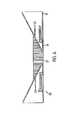
- FIG. 3is a schematic illustration of the passage of a patterned beam of radiation from an optical element through a second fluid, a transparent plate, and first fluid incident on a substrate;
- FIG. 4is a schematic illustration of a system for providing fluid between the projection system and the transparent plate
- FIG. 5is an enlarged view of the system of FIG. 4 ;
- FIG. 6is a schematic illustration of a system for providing fluid between the transparent plate and the substrate.
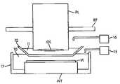
- FIG. 1schematically depicts a lithographic projection apparatus 1 according to an embodiment of the invention.
- the apparatusincludes a radiation system Ex, IL constructed and arranged to supply a beam PB of radiation (e.g. UV or EUV radiation, such as, for example, generated by an excimer laser operating at a wavelength of 248 nm, 193 nm or 157 nm, or by a laser-fired plasma source operating at 13.6 nm).
- the radiation systemalso comprises a radiation source LA.
- the apparatusalso includes a first object (mask) table MT provided with a mask holder constructed and arranged to hold a mask MA (e.g.
- the projection system or lens PLe.g. a quartz and/or CaF 2 lens system or a refractive or catadioptric system, a mirror group or an array of field deflectors
- the projection system PLis constructed and arranged to image an irradiated portion of the mask MA onto a target portion C (e.g. comprising one or more dies) of the substrate W.
- the projection system PLis supported on a reference frame RF.
- the apparatusmay employ another kind of patterning device, such as a programmable mirror array of a type as referred to above.
- the source LA(e.g. a UV excimer laser, an undulator or wiggler provided around the path of an electron beam in a storage ring or synchrotron, a laser-produced plasma source, a discharge source or an electron or ion beam source) produces radiation.
- the radiationis fed into an illumination system (illuminator) IL, either directly or after having traversed a conditioner, such as a beam expander Ex, for example.
- the illuminator ILmay comprise an adjusting device AM for setting the outer and/or inner radial extent (commonly referred to as ⁇ -outer and ⁇ -inner, respectively) of the intensity distribution in the beam.
- itwill generally comprise various other components, such as an integrator IN and a condenser CO.
- the beam PB impinging on the mask MAhas a desired uniformity and intensity distribution in its cross-section.
- the source LAmay be within the housing of the lithographic projection apparatus (as is often the case when the source LA is a mercury lamp, for example), but that it may also be remote from the lithographic projection apparatus, the radiation beam which it produces being led into the apparatus (e.g. with the aid of suitable directing mirrors).
- the latter scenariois often the case when the source LA is an excimer laser.
- the present inventionencompasses both of these scenarios.
- the present inventionencompasses embodiments wherein the radiation system Ex, IL is adapted to supply a beam of radiation having a wavelength of less than about 170 nm, such as with wavelengths of 157 nm, 126 nm and 13.6 nm, for example.
- the beam PBsubsequently intercepts the mask MA, which is held on the mask table MT. Having traversed the mask MA, the beam PB passes through the lens PL, which focuses the beam PB onto a target portion C of the substrate W. With the aid of the second positioning device PW and interferometer IF, the substrate table WT can be moved accurately, e.g. so as to position different target portions C in the path of the beam PB. Similarly, the first positioning device PM can be used to accurately position the mask MA with respect to the path of the beam PB, e.g. after mechanical retrieval of the mask MA from a mask library, or during a scan.
- the mask table MTmay just be connected to a short stroke actuator, or may be fixed.
- the mask MA and the substrate Wmay be aligned using mask alignment marks M 1 , M 2 and substrate alignment marks P 1 , P 2 .
- the depicted apparatuscan be used in two different modes:
- the substrate table WTis immersed in a first fluid 10 having a first index of refraction.
- the first fluid 10is provided by a first fluid supply system 15 .
- a transparent plate, or dish, 12is positioned between the projection system PL and the substrate table WT.
- the space between an optical element OE (e.g., a lens) of the projection system PL and the transparent plate 12is filled with a second fluid 11 having a second index of refraction.
- the second index of refractionis different from the first index of refraction.
- the second fluid 11is provided by a second fluid supply system 16 .
- the transparent plate 12has a third index of refraction that is preferably between the first index of refraction of the first fluid 10 and the second index of refraction of the second fluid 11 .
- an optical element OE of the projection system PLhas a index of refraction n OE and the substrate W has an index of refraction n W that is larger than the index of refraction n OE of the optical element OE.
- the optical elementfor example a lens, may be formed, for example, of glass, fused silica, quartz, or CaF 2 , and have, for example a index of refraction n OE of about 1.4 to about 1.6.
- the optical element OEmay be formed of, for example, fused silica, commonly used in deep ultraviolet (DUV) lithography, and have an index of refraction n OE of about 1.46.
- the optical element OEmay be formed of CaF 2 , commonly used in 157 nm lithography, and have an index of refraction n OE ranging from about 1.4 to about 1.56.
- the second fluid 11may be, for example, water and have an index of refraction n SL of about 1.3 to 1.35 for use with radiation having a wavelength of 248 nm. In the case of using water as the second fluid 11 with radiation having a wavelength of, for example 193 nm, the index of refraction n SL should be approximately 1.44.
- the index of refraction n W of the substrate Wmay be, for example, between 1.7 to 1.8.
- the first fluid 10has an index of refraction n FL that may be relatively higher than the index of refraction n SL of the second fluid 11 .
- the first fluid 10may be a perfluoropolyether (PFPE) fluid.
- PFPEperfluoropolyether
- the PFPE fluidmay be, for example, FOMBLIN® or GALDEN®, available from Ausimont Corporation, or KRYTOX®, available from DuPont.
- PFPE fluidsare currently used as lubricants in vacuum pumps and thus are compatible with clean room environments in which photolithographic projection apparatus are used. PFPE fluids are optically clean, non-toxic, chemically inert, and compatible with at least some current resist materials.
- PFPE fluidsalso have an index of refraction that is closely matched to CaF 2 , commonly used to form optical elements of the projection system in 193 nm lithography for color correction and commonly used for optical elements in 157 nm lithography.
- PFPE fluidsare chemical and solvent resistant. They also have excellent thermal and electrical resistance and are non-reactive with metal, plastic, elastomers and rubber.
- PFPE fluidsare inert to liquid and gaseous oxygen and are nonflammable. Because PFPE fluids are inert to liquid and gaseous oxygen they are not affected by the high oxygen conditions found in photo-resist stripping processes.
- PFPE fluidscan also withstand Lewis acids produced during aluminum etching, products from sulfur, most acids, most bases and most oxidizing agents. They are available in a variety of viscosities and have low evaporation loss. PFPE fluids also have excellent radiation hardness and resistance to polymerization in the presence of ionizing radiation. PFPE fluids have zero ozone depletion potential and are not classified as volatile organic chemicals by the Environmental Protection Agency.
- the transparent plate 12has an index of refraction n TP that is between the index of refraction n FL of the first fluid 10 and the index of refraction n SL of the second fluid 11 .
- the transparent plate 12may be formed of any material that is transparent to the particular wavelength radiation, e.g., 365 nm, 248 nm, 193 nm, 157, or 126 nm, generated by the radiation system Ex, IL of the lithographic projection apparatus 1 and has an index of refraction n TP between the indices of refraction of the first fluid 10 and the second fluid 11 , including an index of refraction n TP being equal to either the index of refraction n FL or n SL of the first fluid 10 or the second fluid 11 , respectively. It should also be appreciated that the entire plate 12 need not be transparent, only those portions through which the patterned projection beam passes through.
- the patterned beam PPBexits the optical element OE of the projection system PL and enters the second fluid 11 .
- the patterned beam PPBpasses the boundary between the optical element OE and the second fluid 11 and passes into the second fluid 11 , it is deflected as its velocity changes upon entering the second fluid 111 . It should be appreciated that if the index of refraction n SL of the second fluid 11 is equal to the index of refraction n OE of the optical element OE, the patterned beam PPB will not be deflected.
- the transparent plate 12may have an index of refraction n TP that is equal to or higher than the index of refraction n SL of the second fluid 11 . As the patterned beam PPB passes from the second fluid 11 into the transparent plate 12 it is deflected. It should be appreciated that the index of refraction n TP of the transparent plate 12 may be equal to the index of refraction n SL of the second fluid 11 in which case the patterned beam PPB will not be deflected upon entering the transparent plate 12 .
- the first fluid 10has an index of refraction n FL that may be equal to or higher than the index of refraction n TP of the transparent plate 12 . If the index of refraction n TP of the transparent plate 12 is equal to the index of refraction n SL of the second fluid 11 , the index of refraction n FL of the first fluid 10 must be higher than the index of refraction n TP of the transparent plate 12 to provide a variable index of refraction. If the index of refraction n FL of the first fluid 10 is higher than the index of refraction n TP of the transparent plate 12 , the patterned beam PPB is deflected as it leaves the transparent plate 12 and enters the first fluid 10 . The patterned beam PPB passes through the first fluid 10 and is then incident on the substrate W.
- first fluid 10has been described as a PFPE fluid and the second fluid 11 has been described as water, it will be appreciated that the first and second fluids 10 and 11 may both be PFPE fluids, or any other fluid of suitable transparency to the wavelength of radiation provided by the radiation system of the apparatus, as long as the index of refraction n FL of the first fluid 10 is different than the index of refraction n SL of the second fluid 11 . It should also be appreciated that the first and second fluids 10 and 11 are selected based on their indices of refraction relative to the indices of refraction of the substrate W and the optical element OE of the projection system PL, respectively. The first fluid 10 should have an index of refraction similar to the index of refraction of the substrate and the second fluid should have an index of refraction similar to the index of refraction of the optical element as possible.
- the index of refraction from the optical element, to the second fluid, to the translucent plate, to the second fluid, and to the waferis thus continuously varied.
- Any combination of indices of refraction of the optical element, the second fluid, the translucent plate, the first fluid and the substrate that produces a variable index of refraction between the optical element and substrate so as to increase the angle of incidence of the patterned projection beam on the substrateis contemplated by the invention.
- the effect of this continuously varying index of refractionis an increase in the angle of incidence of the patterned projection beam on the substrate, a decrease of reflection of the patterned projection beam by the substrate, and an increase in the resolution of the apparatus.
- first and second fluidsmay be varied (e.g. by the fluid supplies 15 and/or 16 ) to further vary the index of refraction from the optical element to the substrate.
- depth (thickness) of the translucent platemay be varied to further vary the index of refraction from the optical element to the substrate.
- FIG. 4shows the second fluid 11 between the projection system PL and the transparent plate 12 .
- a fluid reservoir 20is filled with the second fluid 11 provided via inlet/outlet ports 23 .
- the reservoir 20forms a contactless seal to the transparent plate 12 around the image field of the projection system PL so that fluid is confined to fill the space between the transparent plate 12 and the optical element of the projection system PL.
- the reservoir 20is formed by a seal member 21 positioned below and surrounding the optical element of the projection system PL.
- the second fluid 11is brought into the space below the projection system PL and within the seal member 21 .
- the seal member 21extends a little above the optical element of the projection system PL and the fluid level rises above the optical element so that a buffer of fluid is provided.
- the seal member 21has an inner periphery that at the upper end closely conforms to the optical element and may be round, for example. At the bottom, the inner periphery closely conforms to the shape of the image field and may be rectangular, for example.
- the first fluid 11is confined to the reservoir by a gas seal 26 between the bottom of the seal member 21 and the surface of the transparent plate 12 .
- the gas seal 26is formed by gas, e.g. air or synthetic air, provided under pressure via inlet 25 to the gap between the seal member 12 and extracted via outlet 24 .
- the overpressure on the gas inlet 25 , vacuum level on the outlet 24 and geometry of the gapare arranged so that there is a high-velocity air flow inwards that confines the fluid. This shown in more detail in FIG. 5 .
- the gas seal 26is formed by two annular grooves 28 , 29 which are connected to the inlet 25 and outlet 24 , respectively, by a series of small conducts spaced around the grooves.
- a large annular hollow in the seal member 21may be provided in each of the inlet 25 and outlet 24 to form a manifold.
- a gap G 1on the outer side of the gas inlet 25 , is small and long so as to provide resistance to air flow outwards.
- a gap G 2at the radius of the inlet 25 , is a little larger to ensure a sufficient distribution of gas around the seal member 21 .
- the inlet 25is formed by a number of small holes around the seal member 21 .
- a gap G 3is chosen to control the gas flow through the seal.
- a gap G 4is larger, to provide a good distribution of vacuum.
- the outlet 24is formed of a number of small holes in the same manner as the inlet 15 .
- a gap G 5is small, to prevent gas bubbles entering the space, and in this embodiment to ensure that capillary action will always fill it with fluid.
- the gas seal 26is thus a balance between the capillary forces pulling fluid into the gap and the airflow pushing liquid out. As the gap widens from G 5 to G 4 , the capillary forces decrease and the airflow increases so that the fluid boundary will lie in this region and be stable under the projection system PL.
- the pressure difference between the inlet at the gap G 2 and the outlet at the gap G 4 as well as the size and geometry of the gap G 3determine the gas flow through the seal 26 and will be determined according to the specific embodiment.
- a possible advantageis achieved if the length of the gap G 3 is short and the absolute pressure at the gap G 2 is twice that at the gap G 4 , in which case the gas velocity will be the speed of sound in the gas and cannot rise any higher. A stable gas flow will therefore be achieved.
- the gas outlet systemcan also be used to completely remove the fluid from the system by reducing the gas inlet pressure and allowing the fluid to enter the gap G 4 and be sucked out by the vacuum system, which can easily be arranged to handle the fluid as well as the gas used to form the seal.
- Control of the pressure in the gas seal 26can also be used to ensure a flow of fluid through the gap G 5 so that fluid in this gap does not disturb the temperature of the fluid in the main space below the projection system.
- the shape of the seal member 21 around the gas inlet 25 and outlet 24should be chosen to provide laminar flow as far as possible so as to reduce turbulence and vibration. Also, the gas flow should be arranged so that the change in flow direction at the fluid interface is as large as possible to provide maximum force confining the fluid.
- FIGS. 4 and 5a similar system as shown in FIGS. 4 and 5 is between the substrate W and the transparent plate 12 .
- the system shown in FIGS. 4 and 5is more fully described in U.S. patent application Ser. No. 10/705,805, filed Nov. 12, 2003, the entire contents of which are incorporated herein by reference.
- FIG. 6shows a cover plate 27 provided on the substrate table WT.
- the cover plate 27has an upper surface coplanar with the substrate W and is closely adjacent to the edge of the substrate W so that there is no sudden loss of fluid as the edge of the substrate W moves under the projection system PL.
- a vacuum outletis preferably provided under the gap between the substrate W and cover plate 27 to remove any fluid passing into the gap and any gas from the gas seal to prevent it from entering the space.
- a device manufacturing methodincludes providing the substrate W at least partially covered by a layer of radiation-sensitive material.
- the patterned beam PPBis projected onto a target portion of the layer of radiation-sensitive material using the projection system.
- the space between an optical element of the projection system and the substrateis filled with at least two fluids.
- the two fluidshave different indices of refraction.
- the transparent plateseparates the two fluids.
- the device manufacturing method of the present inventionmay be preceded by design of the functions and performance of the device and a pattern to realize the functions. It will also be appreciated that the design and manufacture of a mask according to the present invention may also precede the method. It will also be appreciated that substrate, or wafer, production and processing may precede the method.
- the wafer processingmay include, for example, oxidizing the wafer surface, forming an insulation film on the wafer surface, forming an electrode, such as by vacuum deposition, on the wafer, implanting ions into the wafer, and doping the wafer with a photosensitive agent.
- Other wafer processing steps that may follow the methodinclude developing the resist, removing the developed resist, such as by etching, and removing unnecessary resist after etching. It will also be appreciated that device assembly and inspection, including, for example, dicing, bonding, packaging (chip sealing), and operation and durability check testing, may follow the method.
Landscapes
- Physics & Mathematics (AREA)
- General Physics & Mathematics (AREA)
- Health & Medical Sciences (AREA)
- Engineering & Computer Science (AREA)
- Environmental & Geological Engineering (AREA)
- Epidemiology (AREA)
- Public Health (AREA)
- Exposure And Positioning Against Photoresist Photosensitive Materials (AREA)
- Exposure Of Semiconductors, Excluding Electron Or Ion Beam Exposure (AREA)
- Surface Treatment Of Optical Elements (AREA)
Abstract
Description
1. Field of the Invention
The present invention relates to a lithographic apparatus, in particular to a lithographic apparatus in which the space between an optical element of a projection system and a substrate is filled with at least two fluids having different indices of refraction. The present invention also relates to a device manufacturing method.
2. Description of the Related Art
The term “patterning device” as here employed should be broadly interpreted as referring to device that can be used to endow an incoming radiation beam with a patterned cross-section, corresponding to a pattern that is to be created in a target portion of the substrate. The term “light valve” can also be used in this context. Generally, the pattern will correspond to a particular functional layer in a device being created in the target portion, such as an integrated circuit or other device. An example of such a patterning device is a mask. The concept of a mask is well known in lithography, and it includes mask types such as binary, alternating phase shift, and attenuated phase shift, as well as various hybrid mask types. Placement of such a mask in the radiation beam causes selective transmission (in the case of a transmissive mask) or reflection (in the case of a reflective mask) of the radiation impinging on the mask, according to the pattern on the mask. In the case of a mask, the support will generally be a mask table, which ensures that the mask can be held at a desired position in the incoming radiation beam, and that it can be moved relative to the beam if so desired.
Another example of a patterning device is a programmable mirror array. One example of such an array is a matrix-addressable surface having a viscoelastic control layer and a reflective surface. The basic principle behind such an apparatus is that, for example, addressed areas of the reflective surface reflect incident light as diffracted light, whereas unaddressed areas reflect incident light as undiffracted light. Using an appropriate filter, the undiffracted light can be filtered out of the reflected beam, leaving only the diffracted light behind. In this manner, the beam becomes patterned according to the addressing pattern of the matrix addressable surface. An alternative embodiment of a programmable mirror array employs a matrix arrangement of tiny mirrors, each of which can be individually tilted about an axis by applying a suitable localized electric field, or by employing piezoelectric actuators. Once again, the mirrors are matrix addressable, such that addressed mirrors will reflect an incoming radiation beam in a different direction to unaddressed mirrors. In this manner, the reflected beam is patterned according to the addressing pattern of the matrix-addressable mirrors. The required matrix addressing can be performed using suitable electronics. In both of the situations described hereabove, the patterning device can comprise one or more programmable mirror arrays. More information on mirror arrays as here referred to can be seen, for example, from U.S. Pat. Nos. 5,296,891 and 5,523,193, and PCT publications WO 98/38597 and WO 98/33096. In the case of a programmable mirror array, the support structure may be embodied as a frame or table, for example, which may be fixed or movable as required.
Another example of a patterning device is a programmable LCD array. An example of such a construction is given in U.S. Pat. No. 5,229,872. As above, the support structure in this case may be embodied as a frame or table, for example, which may be fixed or movable as required.
For purposes of simplicity, the rest of this text may, at certain locations, specifically direct itself to examples involving a mask and mask table. However, the general principles discussed in such instances should be seen in the broader context of the patterning device as hereabove set forth.
Lithographic projection apparatus can be used, for example, in the manufacture of integrated circuits (ICs). In such a case, the patterning device may generate a circuit pattern corresponding to an individual layer of the IC, and this pattern can be imaged onto a target portion (e.g. comprising one or more dies) on a substrate (silicon wafer) that has been coated with a layer of radiation sensitive material (resist). In general, a single wafer will contain a whole network of adjacent target portions that are successively irradiated via the projection system, one at a time. In current apparatus, employing patterning by a mask on a mask table, a distinction can be made between two different types of machine. In one type of lithographic projection apparatus, each target portion is irradiated by exposing the entire mask pattern onto the target portion at once. Such an apparatus is commonly referred to as a wafer stepper. In an alternative apparatus, commonly referred to as a step and scan apparatus, each target portion is irradiated by progressively scanning the mask pattern under the beam of radiation in a given reference direction (the “scanning” direction) while synchronously scanning the substrate table parallel or anti-parallel to this direction. Since, in general, the projection system will have a magnification factor M (generally <1), the speed V at which the substrate table is scanned will be a factor M times that at which the mask table is scanned. More information with regard to lithographic devices as here described can be seen, for example, from U.S. Pat. No. 6,046,792.
In a known manufacturing process using a lithographic projection apparatus, a pattern (e.g. in a mask) is imaged onto a substrate that is at least partially covered by a layer of radiation sensitive material (resist). Prior to this imaging, the substrate may undergo various procedures, such as priming, resist coating and a soft bake. After exposure, the substrate may be subjected to other procedures, such as a post-exposure bake (PEB), development, a hard bake and measurement and/or inspection of the imaged features. This array of procedures is used as a basis to pattern an individual layer of a device, e.g. an IC. Such a patterned layer may then undergo various processes such as etching, ion-implantation (doping), metallization, oxidation, chemical, mechanical polishing, etc., all intended to finish off an individual layer. If several layers are required, then the whole procedure, or a variant thereof, will have to be repeated for each new layer. It is important to ensure that the overlay (juxtaposition) of the various stacked layers is as accurate as possible. For this purpose, a small reference mark is provided at one or more positions on the wafer, thus defining the origin of a coordinate system on the wafer. Using optical and electronic devices in combination with the substrate holder positioning device (referred to hereinafter as “alignment system”), this mark can then be relocated each time a new layer has to be juxtaposed on an existing layer, and can be used as an alignment reference. Eventually, an array of devices will be present on the substrate (wafer). These devices are then separated from one another by a technique such as dicing or sawing, whence the individual devices can be mounted on a carrier, connected to pins, etc. Further information regarding such processes can be obtained, for example, from the book “Microchip Fabrication: A Practical Guide to Semiconductor Processing”, Third Edition, by Peter van Zant, McGraw Hill Publishing Co., 1997, ISBN 0-07-067250-4.
For the sake of simplicity, the projection system may hereinafter be referred to as the “lens.” However, this term should be broadly interpreted as encompassing various types of projection system, including refractive optics, reflective optics, and catadioptric systems, for example. The radiation system may also include components operating according to any of these design types for directing, shaping or controlling the projection beam of radiation, and such components may also be referred to below, collectively or singularly, as a “lens.” Further, the lithographic apparatus may be of a type having two or more substrate tables (and/or two or more mask tables). In such “multiple stage” devices the additional tables may be used in parallel or preparatory steps may be carried out on one or more tables while one or more other tables are being used for exposures. Dual stage lithographic apparatus are described, for example, in U.S. Pat. Nos. 5,969,441 and 6,262,796.
In order to increase the degree of integration of semiconductor devices and keep pace with Moore's law, it will be necessary to provide lithographic projection apparatus capable of printing practical minimum line widths of 25-100 nm. Currently available photolithographic tools using 193 nm and 157 nm radiation can produce pattern features having a resolution (in nm) according to the well known equation R=k1·λ/NA, where R is the resolution, k1is a constant that is dependent on the radiation sensitive material (resist) used, λ is the wavelength of the radiation, and NA is the numerical aperture. The numerical aperture NA is determined according to the equation NA=n·sin θ, where n is the index of refraction of the material through which the radiation passes and θ is the angle of incidence of the radiation. A lower limit of k1is 0.25 and lithographic projection apparatus having a NA of 0.85 are currently available. Difficulties in optical design make increasing the NA difficult. As k1and NA are generally considered to be at their limits, the ability to decrease the resolution, i.e, print smaller pattern features, of lithographic projection apparatus appears to be dependent on decreasing the wavelength λ of the radiation.
One method of decreasing the wavelength of the radiation is to immerse the substrate in a lithographic projection apparatus in a fluid having a relatively high refractive index, e.g., water, so as to fill the space between the optical element of the projection system (lens) and the substrate. Filling the space between the optical element of the projection system and the substrate enables the imaging of smaller features as the exposure radiation has a shorter wavelength in the fluid. The effect of the fluid may be regarded as increasing the effective NA of the system. This method can also be used to increase the depth of focus for imaging at the same resolution. The depth of focus is defined by the equation DOF=+/−k2λNA2, where k2is a process dependent constant, λ is wavelength, and NA is numerical aperture. Depth of focus is one of the factors determining the resolution of the lithographic apparatus and is defined as the distance along the optical axis over which the image of the pattern is adequately sharp.
One difficulty presented by filling the space between the optical element of the projection system and the substrate with a fluid is the fluid has an index of refraction between the indices of refraction of the optical element and the substrate. The index of refraction of the fluid may not be sufficient to improve the resolution of the image. The fluid is only able to provide a single decrease in the wavelength of the radiation as the index of refraction of the fluid is constant throughout the space between the optical element and the substrate.
Another problem associated with immersion lithography is that many fluids are insufficiently transparent to 193 nm and 157 nm radiation which would tend to decrease the amount of radiation incident on the substrate.
It is an aspect of the present invention to provide a lithographic apparatus in which the space between the optical element of the projection system is filled with at least two fluids having different indices of refraction in order to increase the angle of incidence of the radiation on the substrate, thus reducing reflection of the radiation by the wafer and increasing the resolution of the apparatus. As used herein, the term fluid refers to liquids, gases, and/or gels.
This and other aspects are achieved according to the invention in a lithographic apparatus including a radiation system constructed and arranged to supply a beam of radiation; a support constructed and arranged to support a patterning device, the patterning device constructed and arranged to pattern the beam of radiation according to a desired pattern; a substrate table to hold a substrate; a projection system constructed and arranged to project the patterned beam onto a target portion of the substrate; a transparent plate positioned between an optical element of the projection system and the substrate; a first fluid having a first index of refraction filling a first space between the substrate and the transparent plate; and a second fluid having a second index of refraction filling a second space between the transparent plate and the optical element.
According to a further aspect of the invention there is provided a device manufacturing method including projecting a patterned beam of radiation onto a target portion of a layer of radiation-sensitive material at least partially covering substrate using a projection system; and filling a space between an optical element of the projection system and the substrate with at least two fluids, wherein the two fluids have different indices of refraction.
Although specific reference may be made in this text to the use of the apparatus according to the invention in the manufacture of ICs, it should be explicitly understood that such an apparatus has many other possible applications. For example, it may be employed in the manufacture of integrated optical systems, guidance and detection patterns for magnetic domain memories, liquid crystal display panels, thin film magnetic heads, etc. n will appreciate that, in the context of such alternative applications, any use of the terms “reticle”, “wafer” or “die” in this text should be considered as being replaced by the more general terms “mask”, “substrate” and “target portion”, respectively.
In the present document, the terms “radiation” and “beam” are used to encompass all types of electromagnetic radiation, including ultraviolet radiation (e.g. with a wavelength of 365, 248, 193, 157 or 126 nm) and EUV (extreme ultra-violet radiation, e.g. having a wavelength in the range 5-20 nm), as well as particle beams, such as ion beams or electron beams.
Embodiments of the invention will now be described, by way of example only, with reference to the accompanying schematic drawings in which:
In the Figures, corresponding reference symbols indicate corresponding parts.
The source LA (e.g. a UV excimer laser, an undulator or wiggler provided around the path of an electron beam in a storage ring or synchrotron, a laser-produced plasma source, a discharge source or an electron or ion beam source) produces radiation. The radiation is fed into an illumination system (illuminator) IL, either directly or after having traversed a conditioner, such as a beam expander Ex, for example. The illuminator IL may comprise an adjusting device AM for setting the outer and/or inner radial extent (commonly referred to as σ-outer and σ-inner, respectively) of the intensity distribution in the beam. In addition, it will generally comprise various other components, such as an integrator IN and a condenser CO. In this way, the beam PB impinging on the mask MA has a desired uniformity and intensity distribution in its cross-section.
It should be noted with regard toFIG. 1 that the source LA may be within the housing of the lithographic projection apparatus (as is often the case when the source LA is a mercury lamp, for example), but that it may also be remote from the lithographic projection apparatus, the radiation beam which it produces being led into the apparatus (e.g. with the aid of suitable directing mirrors). The latter scenario is often the case when the source LA is an excimer laser. The present invention encompasses both of these scenarios. In particular, the present invention encompasses embodiments wherein the radiation system Ex, IL is adapted to supply a beam of radiation having a wavelength of less than about 170 nm, such as with wavelengths of 157 nm, 126 nm and 13.6 nm, for example.
The beam PB subsequently intercepts the mask MA, which is held on the mask table MT. Having traversed the mask MA, the beam PB passes through the lens PL, which focuses the beam PB onto a target portion C of the substrate W. With the aid of the second positioning device PW and interferometer IF, the substrate table WT can be moved accurately, e.g. so as to position different target portions C in the path of the beam PB. Similarly, the first positioning device PM can be used to accurately position the mask MA with respect to the path of the beam PB, e.g. after mechanical retrieval of the mask MA from a mask library, or during a scan. In general, movement of the object tables MT, WT will be realized with the aid of a long-stroke module (coarse positioning) and a short-stroke module (fine positioning). However, in the case of a wafer stepper (as opposed to a step and scan apparatus) the mask table MT may just be connected to a short stroke actuator, or may be fixed. The mask MA and the substrate W may be aligned using mask alignment marks M1, M2and substrate alignment marks P1, P2.
The depicted apparatus can be used in two different modes:
- 1. In step mode, the mask table MT is kept essentially stationary, and an entire mask image is projected at once, i.e. a single “flash,” onto a target portion C. The substrate table WT is then shifted in the X and/or Y directions so that a different target portion C can be irradiated by the beam PB;
- 2. In scan mode, essentially the same scenario applies, except that a given target portion C is not exposed in a single “flash.” Instead, the mask table MT is movable in a given direction (the so-called “scan direction”, e.g. the Y direction) with a speed v, so that the beam PB is caused to scan over a mask image. Concurrently, the substrate table WT is simultaneously moved in the same or opposite direction at a speed V=Mv, in which M is the magnification of the lens PL (typically, M=¼ or ⅕). In this manner, a relatively large target portion C can be exposed, without having to compromise on resolution.
Referring toFIG. 2 , the substrate table WT is immersed in afirst fluid 10 having a first index of refraction. Thefirst fluid 10 is provided by a firstfluid supply system 15. A transparent plate, or dish,12 is positioned between the projection system PL and the substrate table WT. The space between an optical element OE (e.g., a lens) of the projection system PL and thetransparent plate 12 is filled with asecond fluid 11 having a second index of refraction. The second index of refraction is different from the first index of refraction. Thesecond fluid 11 is provided by a secondfluid supply system 16. Thetransparent plate 12 has a third index of refraction that is preferably between the first index of refraction of thefirst fluid 10 and the second index of refraction of thesecond fluid 11.
Referring toFIG. 3 , an optical element OE of the projection system PL has a index of refraction nOEand the substrate W has an index of refraction nWthat is larger than the index of refraction nOEof the optical element OE. The optical element, for example a lens, may be formed, for example, of glass, fused silica, quartz, or CaF2, and have, for example a index of refraction nOEof about 1.4 to about 1.6. The optical element OE may be formed of, for example, fused silica, commonly used in deep ultraviolet (DUV) lithography, and have an index of refraction nOEof about 1.46. As another example, the optical element OE may be formed of CaF2, commonly used in 157 nm lithography, and have an index of refraction nOEranging from about 1.4 to about 1.56.
Thesecond fluid 11 may be, for example, water and have an index of refraction nSLof about 1.3 to 1.35 for use with radiation having a wavelength of 248 nm. In the case of using water as thesecond fluid 11 with radiation having a wavelength of, for example 193 nm, the index of refraction nSLshould be approximately 1.44. The index of refraction nWof the substrate W may be, for example, between 1.7 to 1.8.
Thefirst fluid 10 has an index of refraction nFLthat may be relatively higher than the index of refraction nSLof thesecond fluid 11. Thefirst fluid 10 may be a perfluoropolyether (PFPE) fluid. The PFPE fluid may be, for example, FOMBLIN® or GALDEN®, available from Ausimont Corporation, or KRYTOX®, available from DuPont. PFPE fluids are currently used as lubricants in vacuum pumps and thus are compatible with clean room environments in which photolithographic projection apparatus are used. PFPE fluids are optically clean, non-toxic, chemically inert, and compatible with at least some current resist materials. PFPE fluids have a 157 nm absorbance α=10−3μm−1base10, which is a thousands times lower than current experimental 157 nm resists. FOMBLIN® Z-25 has an index of refraction at 157 nm of n=1.35. FOMBLIN® Y-18 has an index of refraction at 157 nm of n=1.37. FOMBLIN® Y-140, a higher molecular weight version, has an index of refraction at 157 nm of n=1.38.
PFPE fluids also have an index of refraction that is closely matched to CaF2, commonly used to form optical elements of the projection system in 193 nm lithography for color correction and commonly used for optical elements in 157 nm lithography. PFPE fluids are chemical and solvent resistant. They also have excellent thermal and electrical resistance and are non-reactive with metal, plastic, elastomers and rubber. PFPE fluids are inert to liquid and gaseous oxygen and are nonflammable. Because PFPE fluids are inert to liquid and gaseous oxygen they are not affected by the high oxygen conditions found in photo-resist stripping processes. PFPE fluids can also withstand Lewis acids produced during aluminum etching, products from sulfur, most acids, most bases and most oxidizing agents. They are available in a variety of viscosities and have low evaporation loss. PFPE fluids also have excellent radiation hardness and resistance to polymerization in the presence of ionizing radiation. PFPE fluids have zero ozone depletion potential and are not classified as volatile organic chemicals by the Environmental Protection Agency.
Thetransparent plate 12 has an index of refraction nTPthat is between the index of refraction nFLof thefirst fluid 10 and the index of refraction nSLof thesecond fluid 11. Thetransparent plate 12 may be formed of any material that is transparent to the particular wavelength radiation, e.g., 365 nm, 248 nm, 193 nm, 157, or 126 nm, generated by the radiation system Ex, IL of the lithographic projection apparatus1 and has an index of refraction nTPbetween the indices of refraction of thefirst fluid 10 and thesecond fluid 11, including an index of refraction nTPbeing equal to either the index of refraction nFLor nSLof thefirst fluid 10 or thesecond fluid 11, respectively. It should also be appreciated that theentire plate 12 need not be transparent, only those portions through which the patterned projection beam passes through.
As shown inFIG. 3 , the patterned beam PPB exits the optical element OE of the projection system PL and enters thesecond fluid 11. As the patterned beam PPB passes the boundary between the optical element OE and thesecond fluid 11 and passes into thesecond fluid 11, it is deflected as its velocity changes upon entering the second fluid111. It should be appreciated that if the index of refraction nSLof thesecond fluid 11 is equal to the index of refraction nOEof the optical element OE, the patterned beam PPB will not be deflected.
Thetransparent plate 12 may have an index of refraction nTPthat is equal to or higher than the index of refraction nSLof thesecond fluid 11. As the patterned beam PPB passes from thesecond fluid 11 into thetransparent plate 12 it is deflected. It should be appreciated that the index of refraction nTPof thetransparent plate 12 may be equal to the index of refraction nSLof thesecond fluid 11 in which case the patterned beam PPB will not be deflected upon entering thetransparent plate 12.
Thefirst fluid 10 has an index of refraction nFLthat may be equal to or higher than the index of refraction nTPof thetransparent plate 12. If the index of refraction nTPof thetransparent plate 12 is equal to the index of refraction nSLof thesecond fluid 11, the index of refraction nFLof thefirst fluid 10 must be higher than the index of refraction nTPof thetransparent plate 12 to provide a variable index of refraction. If the index of refraction nFLof thefirst fluid 10 is higher than the index of refraction nTPof thetransparent plate 12, the patterned beam PPB is deflected as it leaves thetransparent plate 12 and enters thefirst fluid 10. The patterned beam PPB passes through thefirst fluid 10 and is then incident on the substrate W.
Although thefirst fluid 10 has been described as a PFPE fluid and thesecond fluid 11 has been described as water, it will be appreciated that the first andsecond fluids first fluid 10 is different than the index of refraction nSLof thesecond fluid 11. It should also be appreciated that the first andsecond fluids first fluid 10 should have an index of refraction similar to the index of refraction of the substrate and the second fluid should have an index of refraction similar to the index of refraction of the optical element as possible.
The index of refraction from the optical element, to the second fluid, to the translucent plate, to the second fluid, and to the wafer is thus continuously varied. Any combination of indices of refraction of the optical element, the second fluid, the translucent plate, the first fluid and the substrate that produces a variable index of refraction between the optical element and substrate so as to increase the angle of incidence of the patterned projection beam on the substrate is contemplated by the invention. The effect of this continuously varying index of refraction is an increase in the angle of incidence of the patterned projection beam on the substrate, a decrease of reflection of the patterned projection beam by the substrate, and an increase in the resolution of the apparatus.
It should be appreciated that more than two fluids may be provided between the optical element and the substrate. The space may be filled with three or more fluids. It should also be appreciated that the three or more fluids may be separated by two or more translucent plates, respectively. It should also be appreciated that the depth of the first and second fluids may be varied (e.g. by the fluid supplies15 and/or16) to further vary the index of refraction from the optical element to the substrate. It should further be appreciated that the depth (thickness) of the translucent plate may be varied to further vary the index of refraction from the optical element to the substrate.
Thereservoir 20 forms a contactless seal to thetransparent plate 12 around the image field of the projection system PL so that fluid is confined to fill the space between thetransparent plate 12 and the optical element of the projection system PL. Thereservoir 20 is formed by aseal member 21 positioned below and surrounding the optical element of the projection system PL. Thesecond fluid 11 is brought into the space below the projection system PL and within theseal member 21. Theseal member 21 extends a little above the optical element of the projection system PL and the fluid level rises above the optical element so that a buffer of fluid is provided. Theseal member 21 has an inner periphery that at the upper end closely conforms to the optical element and may be round, for example. At the bottom, the inner periphery closely conforms to the shape of the image field and may be rectangular, for example.
Thefirst fluid 11 is confined to the reservoir by agas seal 26 between the bottom of theseal member 21 and the surface of thetransparent plate 12. Thegas seal 26 is formed by gas, e.g. air or synthetic air, provided under pressure viainlet 25 to the gap between theseal member 12 and extracted viaoutlet 24. The overpressure on thegas inlet 25, vacuum level on theoutlet 24 and geometry of the gap are arranged so that there is a high-velocity air flow inwards that confines the fluid. This shown in more detail in FIG.5.
Thegas seal 26 is formed by twoannular grooves inlet 25 andoutlet 24, respectively, by a series of small conducts spaced around the grooves. A large annular hollow in theseal member 21 may be provided in each of theinlet 25 andoutlet 24 to form a manifold.
A gap G1, on the outer side of thegas inlet 25, is small and long so as to provide resistance to air flow outwards. A gap G2, at the radius of theinlet 25, is a little larger to ensure a sufficient distribution of gas around theseal member 21. Theinlet 25 is formed by a number of small holes around theseal member 21. A gap G3 is chosen to control the gas flow through the seal. A gap G4 is larger, to provide a good distribution of vacuum. Theoutlet 24 is formed of a number of small holes in the same manner as theinlet 15. A gap G5 is small, to prevent gas bubbles entering the space, and in this embodiment to ensure that capillary action will always fill it with fluid.
Thegas seal 26 is thus a balance between the capillary forces pulling fluid into the gap and the airflow pushing liquid out. As the gap widens from G5 to G4, the capillary forces decrease and the airflow increases so that the fluid boundary will lie in this region and be stable under the projection system PL.
The pressure difference between the inlet at the gap G2 and the outlet at the gap G4 as well as the size and geometry of the gap G3, determine the gas flow through theseal 26 and will be determined according to the specific embodiment. However, a possible advantage is achieved if the length of the gap G3 is short and the absolute pressure at the gap G2 is twice that at the gap G4, in which case the gas velocity will be the speed of sound in the gas and cannot rise any higher. A stable gas flow will therefore be achieved.
The gas outlet system can also be used to completely remove the fluid from the system by reducing the gas inlet pressure and allowing the fluid to enter the gap G4 and be sucked out by the vacuum system, which can easily be arranged to handle the fluid as well as the gas used to form the seal. Control of the pressure in thegas seal 26 can also be used to ensure a flow of fluid through the gap G5 so that fluid in this gap does not disturb the temperature of the fluid in the main space below the projection system.
The shape of theseal member 21 around thegas inlet 25 andoutlet 24 should be chosen to provide laminar flow as far as possible so as to reduce turbulence and vibration. Also, the gas flow should be arranged so that the change in flow direction at the fluid interface is as large as possible to provide maximum force confining the fluid.
It should be appreciated that a similar system as shown inFIGS. 4 and 5 is between the substrate W and thetransparent plate 12. The system shown inFIGS. 4 and 5 is more fully described in U.S. patent application Ser. No. 10/705,805, filed Nov. 12, 2003, the entire contents of which are incorporated herein by reference.
A device manufacturing method includes providing the substrate W at least partially covered by a layer of radiation-sensitive material. The patterned beam PPB is projected onto a target portion of the layer of radiation-sensitive material using the projection system. The space between an optical element of the projection system and the substrate is filled with at least two fluids. The two fluids have different indices of refraction. The transparent plate separates the two fluids.
It will be appreciated that the device manufacturing method of the present invention may be preceded by design of the functions and performance of the device and a pattern to realize the functions. It will also be appreciated that the design and manufacture of a mask according to the present invention may also precede the method. It will also be appreciated that substrate, or wafer, production and processing may precede the method. The wafer processing may include, for example, oxidizing the wafer surface, forming an insulation film on the wafer surface, forming an electrode, such as by vacuum deposition, on the wafer, implanting ions into the wafer, and doping the wafer with a photosensitive agent. Other wafer processing steps that may follow the method include developing the resist, removing the developed resist, such as by etching, and removing unnecessary resist after etching. It will also be appreciated that device assembly and inspection, including, for example, dicing, bonding, packaging (chip sealing), and operation and durability check testing, may follow the method.
While specific embodiments of the invention have been described above, it will be appreciated that the invention may be practiced otherwise than as described. The description is not intended to limit the invention.
Claims (23)
1. A lithographic projection apparatus, comprising:
a radiation system constructed and arranged to provide a beam of radiation;
a support constructed and arranged to supporting a patterning device, the patterning device constructed and arranged to pattern the beam of radiation according to a desired pattern;
a substrate table constructed and arranged to hold a substrate;
a projection system constructed and arranged to project the patterned beam of radiation onto a target portion of the substrate;
a transparent plate positioned between an optical element of the projection system and the substrate;
a first fluid having a first index of refraction filling a first space between the substrate and the transparent plate; and
a second fluid having a second index of refraction filling a second space between the transparent plate and the optical element, wherein the first and second indices of refraction are different.
2. An apparatus according toclaim 1 , wherein the first index of refraction is greater than the second index of refraction.
3. An apparatus according toclaim 1 , wherein the second index of refraction is greater than the first index of refraction.
4. An apparatus according toclaim 1 , wherein the transparent plate has a third index of refraction.
5. An apparatus according toclaim 4 , wherein the third index of refraction is between the first index of refraction and the second index of refraction.
6. An apparatus according toclaim 4 , wherein the third index of refraction is substantially equal to the first index of refraction.
7. An apparatus according toclaim 4 , wherein the third index of refraction is substantially equal to the second index of refraction.
8. An apparatus according toclaim 1 , wherein the first index of refraction is substantially equal to an index of refraction of the substrate.
9. An apparatus according toclaim 1 , wherein the second index of refraction is substantially equal to an index of refraction of the optical element.
10. An apparatus according toclaim 1 , wherein the first fluid is one of a perfluoropolyether fluid and water and the second fluid is one of a perfluoropolyeter fluid and water.
11. An apparatus according toclaim 1 , wherein the first and second fluids are perfluoropolyether fluids.
12. A device manufacturing method, comprising:
projecting a patterned beam of radiation onto a target portion of a layer of radiation-sensitive material at least partially covering a substrate; and
filling a space between an optical element of a projection system and the substrate with first and second fluids having first and second indices of refraction, respectively, wherein the first and second indices of refraction are different.
13. A device manufacturing method according toclaim 12 , further comprising:
separating the first and second fluids with a transparent plate.
14. A device manufacturing method according toclaim 13 , wherein a first space between the substrate and the transparent plate is filled with the first fluid and a second space between the transparent plate and the optical element is filled with the second fluid.
15. A device manufacturing method according toclaim 12 , wherein the first index of refraction is greater than the second index of refraction.
16. A device manufacturing method according toclaim 12 , wherein the second index of refraction is greater than the first index of refraction.
17. A device manufacturing method according toclaim 14 , wherein the first index of refraction is substantially equal to an index of refraction of the substrate.
18. A device manufacturing method according toclaim 14 , wherein the second index of refraction is substantially equal to an index of refraction of the optical element.
19. A device manufacturing method according toclaim 12 , wherein the first fluid is one of a perfluoropolyether fluid and water and the second fluid is one of a perfluoropolyether fluid and water.
20. A device manufacturing method according toclaim 12 , wherein the first and second fluids are perfluoropolyether fluids.
21. A device manufacturing method according toclaim 13 , wherein the transparent plate has a third index of refraction between the first and second indices of refraction.
22. A device manufacturing method according toclaim 21 , wherein the third index of refraction is substantially equal to the fist index of refraction.
23. A device manufacturing method according toclaim 21 , wherein the third index of refraction is substantially equal to the second index of refraction.
Priority Applications (9)
| Application Number | Priority Date | Filing Date | Title |
|---|---|---|---|
| US10/698,012US6954256B2 (en) | 2003-08-29 | 2003-10-31 | Gradient immersion lithography |
| EP04254940AEP1510871B1 (en) | 2003-08-29 | 2004-08-17 | Lithographic apparatus and device manufacturing method |
| SG200405050ASG109610A1 (en) | 2003-08-29 | 2004-08-23 | Lithographic apparatus and device manufacturing method |
| JP2004247771AJP2005079589A (en) | 2003-08-29 | 2004-08-27 | Lithographic apparatus and device manufacturing method |
| US10/927,531US8208123B2 (en) | 2003-08-29 | 2004-08-27 | Lithographic apparatus and device manufacturing method |
| JP2004247632AJP3946212B2 (en) | 2003-08-29 | 2004-08-27 | Lithographic projection apparatus |
| CNB2004100748555ACN100495213C (en) | 2003-08-29 | 2004-08-30 | Photolithography apparatus and device manufacturing method |
| US11/218,574US7113259B2 (en) | 2003-10-31 | 2005-09-06 | Lithographic apparatus and device manufacturing method |
| JP2008258276AJP2009016871A (en) | 2003-08-29 | 2008-10-03 | Lithographic device and device manufacturing method |
Applications Claiming Priority (2)
| Application Number | Priority Date | Filing Date | Title |
|---|---|---|---|
| EP03255377 | 2003-08-29 | ||
| US10/698,012US6954256B2 (en) | 2003-08-29 | 2003-10-31 | Gradient immersion lithography |
Related Child Applications (1)
| Application Number | Title | Priority Date | Filing Date |
|---|---|---|---|
| US11/218,574ContinuationUS7113259B2 (en) | 2003-10-31 | 2005-09-06 | Lithographic apparatus and device manufacturing method |
Publications (2)
| Publication Number | Publication Date |
|---|---|
| US20050094116A1 US20050094116A1 (en) | 2005-05-05 |
| US6954256B2true US6954256B2 (en) | 2005-10-11 |
Family
ID=34424773
Family Applications (2)
| Application Number | Title | Priority Date | Filing Date |
|---|---|---|---|
| US10/698,012Expired - Fee RelatedUS6954256B2 (en) | 2003-08-29 | 2003-10-31 | Gradient immersion lithography |
| US10/927,531Expired - Fee RelatedUS8208123B2 (en) | 2003-08-29 | 2004-08-27 | Lithographic apparatus and device manufacturing method |
Family Applications After (1)
| Application Number | Title | Priority Date | Filing Date |
|---|---|---|---|
| US10/927,531Expired - Fee RelatedUS8208123B2 (en) | 2003-08-29 | 2004-08-27 | Lithographic apparatus and device manufacturing method |
Country Status (5)
| Country | Link |
|---|---|
| US (2) | US6954256B2 (en) |
| EP (1) | EP1510871B1 (en) |
| JP (3) | JP3946212B2 (en) |
| CN (1) | CN100495213C (en) |
| SG (1) | SG109610A1 (en) |
Cited By (65)
| Publication number | Priority date | Publication date | Assignee | Title |
|---|---|---|---|---|
| US20050042554A1 (en)* | 2003-07-28 | 2005-02-24 | Asml Netherlands B.V. | Lithographic apparatus, device manufacturing method and a substrate |
| US20050073670A1 (en)* | 2003-10-03 | 2005-04-07 | Micronic Laser Systems Ab | Method and device for immersion lithography |
| US20050146693A1 (en)* | 2003-12-09 | 2005-07-07 | Yoshinori Ohsaki | Exposure apparatus |
| US20050219490A1 (en)* | 2002-12-10 | 2005-10-06 | Nikon Corporation | Exposure apparatus and method for producing device |
| US20050237501A1 (en)* | 2004-04-22 | 2005-10-27 | International Business Machines Corporation | Wafer cell for immersion lithography |
| US20050259234A1 (en)* | 2002-12-10 | 2005-11-24 | Nikon Corporation | Exposure apparatus and device manufacturing method |
| US20050286030A1 (en)* | 2004-06-23 | 2005-12-29 | Jen-Chieh Shih | Immersion optical projection system |
| US20060203218A1 (en)* | 2003-08-26 | 2006-09-14 | Nikon Corporation | Optical element and exposure apparatus |
| US20060209281A1 (en)* | 2005-03-18 | 2006-09-21 | Canon Kabushiki Kaisha | Exposure apparatus, exposure method, and device manufacturing method |
| US20060262419A1 (en)* | 2004-01-07 | 2006-11-23 | Olympus Corporation | Objective, optical analyzer, method of driving optical analyzer, and microscope |
| US20060268250A1 (en)* | 2002-11-12 | 2006-11-30 | Asml Netherlands B.V. | Lithographic apparatus and device manufacturing method |
| US20060289794A1 (en)* | 2005-06-10 | 2006-12-28 | International Business Machines Corporation | Immersion lithography with equalized pressure on at least projection optics component and wafer |
| US20070034605A1 (en)* | 2005-08-10 | 2007-02-15 | International Business Machines Corporation | Evaporation control using coating |
| US20070109525A1 (en)* | 2003-12-26 | 2007-05-17 | Toshinobu Tokita | Exposure apparatus and method |
| US7224436B2 (en) | 2002-11-12 | 2007-05-29 | Asml Netherlands B.V. | Lithographic apparatus and device manufacturing method |
| US20080038675A1 (en)* | 2004-02-20 | 2008-02-14 | Nikon Corporation | Exposure Method, Exposure Apparatus, Exposure System and Device Manufacturing Method |
| US20080053150A1 (en)* | 2006-08-31 | 2008-03-06 | Lisa Anne Moore | F-doped silica glass and process of making same |
| US20080218717A1 (en)* | 2003-05-13 | 2008-09-11 | Asml Netherlands B.V. | Lithographic apparatus and device manufacturing method |
| US20080252866A1 (en)* | 2004-12-15 | 2008-10-16 | Asml Netherlands B.V. | Lithographic apparatus and device manufacturing method |
| US20080259292A1 (en)* | 2004-10-18 | 2008-10-23 | Asml Netherlands B.V. | Lithographic apparatus and device manufacturing method |
| US20080271747A1 (en)* | 2007-05-04 | 2008-11-06 | Asml Netherlands B.V. | Cleaning device and a lithographic apparatus cleaning method |
| US20080278696A1 (en)* | 2003-10-28 | 2008-11-13 | Asml Netherlands B.V. | Lithographic apparatus |
| US20080304026A1 (en)* | 2007-03-02 | 2008-12-11 | Canon Kabushiki Kaisha | Immersion exposure apparatus and device manufacturing method |
| US20090002654A1 (en)* | 2005-12-22 | 2009-01-01 | Scott Warrick | Immersion Lithography Apparatus and Method of Performing Immersion Lithography |
| US20090009734A1 (en)* | 2004-11-12 | 2009-01-08 | Asml Netherlands B.V. | Lithographic apparatus and device manufacturing method |
| US20090021707A1 (en)* | 2003-10-15 | 2009-01-22 | Asml Netherlands B.V. | Lithographic apparatus and device manufacturing method |
| US20090033905A1 (en)* | 2004-05-21 | 2009-02-05 | Asml Netherlands B.V. | Lithographic apparatus and device manufacturing method |
| US20090103070A1 (en)* | 2003-08-26 | 2009-04-23 | Nikon Corporation | Optical element and exposure apparatus |
| US20090153823A1 (en)* | 2004-09-24 | 2009-06-18 | Asml Netherlands B.V. | Lithographic apparatus and device manufacturing method |
| US20090201471A1 (en)* | 2004-06-16 | 2009-08-13 | Asml Netherlands B.V. | Vacuum system for immersion photolithography |
| US7593092B2 (en) | 2002-11-12 | 2009-09-22 | Asml Netherlands B.V. | Lithographic apparatus and device manufacturing method |
| US20090251674A1 (en)* | 2003-07-24 | 2009-10-08 | Asml Netherlands B.V. | Lithographic apparatus and device manufacturing method |
| US20090279064A1 (en)* | 2004-11-12 | 2009-11-12 | Asml Netherlands B.V. | Lithographic apparatus and device manufacturing method |
| US20090296061A1 (en)* | 2003-12-23 | 2009-12-03 | Asml Netherlands B.V. | Lithographic apparatus, alignment apparatus, device manufacturing method, and a method of converting an apparatus |
| US20100066988A1 (en)* | 2008-09-17 | 2010-03-18 | Asml Netherlands B.V. | Lithographic apparatus and method of generating the apparatus |
| US7710537B2 (en) | 2004-11-12 | 2010-05-04 | Asml Netherlands B.V. | Lithographic apparatus and device manufacturing method |
| US7812925B2 (en) | 2003-06-19 | 2010-10-12 | Nikon Corporation | Exposure apparatus, and device manufacturing method |
| US20100296067A1 (en)* | 2009-05-01 | 2010-11-25 | Asml Netherlands B.V. | Lithographic apparatus and method of operating the apparatus |
| US20100302519A1 (en)* | 2003-07-16 | 2010-12-02 | Asml Netherlands B.V. | Lithographic apparatus and device manufacturing method |
| US20100321652A1 (en)* | 2003-05-30 | 2010-12-23 | Asml Netherlands B.V. | Lithographic apparatus and device manufacturing method |
| US20110001944A1 (en)* | 2004-12-02 | 2011-01-06 | Asml Netherlands B.V. | Lithographic apparatus and device manufacturing method |
| US20110134402A1 (en)* | 2004-10-05 | 2011-06-09 | Asml Netherlands B.V. | Lithographic apparatus and device manufacturing method |
| US7982850B2 (en) | 2002-11-12 | 2011-07-19 | Asml Netherlands B.V. | Immersion lithographic apparatus and device manufacturing method with gas supply |
| US8011377B2 (en) | 2007-05-04 | 2011-09-06 | Asml Netherlands B.V. | Cleaning device and a lithographic apparatus cleaning method |
| US20110222030A1 (en)* | 2010-03-09 | 2011-09-15 | Nanya Technology Corporation | Immersion lithographic apparatuses |
| US8031325B2 (en) | 2004-08-19 | 2011-10-04 | Asml Netherlands B.V. | Lithographic apparatus and device manufacturing method |
| US8035795B2 (en) | 2003-04-11 | 2011-10-11 | Nikon Corporation | Apparatus and method for maintaining immersion fluid in the gap under the protection lens during wafer exchange in an immersion lithography machine |
| USRE42849E1 (en) | 2004-02-09 | 2011-10-18 | Asml Netherlands B.V. | Lithographic apparatus and device manufacturing method |
| US8045136B2 (en) | 2004-02-02 | 2011-10-25 | Nikon Corporation | Stage drive method and stage unit, exposure apparatus, and device manufacturing method |
| US8045137B2 (en) | 2004-12-07 | 2011-10-25 | Asml Netherlands B.V. | Lithographic apparatus and device manufacturing method |
| US8142852B2 (en) | 2003-07-31 | 2012-03-27 | Asml Netherlands B.V. | Lithographic apparatus and device manufacturing method |
| US8154708B2 (en)* | 2003-06-09 | 2012-04-10 | Asml Netherlands B.V. | Lithographic apparatus and device manufacturing method |
| US8218125B2 (en) | 2003-07-28 | 2012-07-10 | Asml Netherlands B.V. | Immersion lithographic apparatus with a projection system having an isolated or movable part |
| US8319939B2 (en) | 2004-07-07 | 2012-11-27 | Asml Netherlands B.V. | Immersion lithographic apparatus and device manufacturing method detecting residual liquid |
| US20130128256A1 (en)* | 2002-11-12 | 2013-05-23 | Asml Netherlands B.V. | Lithographic apparatus and device manufacturing method |
| US8472006B2 (en) | 2003-11-24 | 2013-06-25 | Asml Netherlands B.V. | Lithographic apparatus and device manufacturing method |
| US8629971B2 (en) | 2003-08-29 | 2014-01-14 | Asml Netherlands B.V. | Lithographic apparatus and device manufacturing method |
| US8804097B2 (en) | 2003-08-29 | 2014-08-12 | Asml Netherlands B.V. | Lithographic apparatus and device manufacturing method |
| US8941810B2 (en) | 2005-12-30 | 2015-01-27 | Asml Netherlands B.V. | Lithographic apparatus and device manufacturing method |
| US8947629B2 (en) | 2007-05-04 | 2015-02-03 | Asml Netherlands B.V. | Cleaning device, a lithographic apparatus and a lithographic apparatus cleaning method |
| US9256136B2 (en) | 2010-04-22 | 2016-02-09 | Asml Netherlands B.V. | Fluid handling structure, lithographic apparatus and device manufacturing method involving gas supply |
| US9482966B2 (en) | 2002-11-12 | 2016-11-01 | Asml Netherlands B.V. | Lithographic apparatus and device manufacturing method |
| USRE46433E1 (en)* | 2002-12-19 | 2017-06-13 | Asml Netherlands B.V. | Method and device for irradiating spots on a layer |
| US10503084B2 (en) | 2002-11-12 | 2019-12-10 | Asml Netherlands B.V. | Lithographic apparatus and device manufacturing method |
| US11216017B2 (en)* | 2019-04-02 | 2022-01-04 | Leica Microsystems Cms Gmbh | Device and method for feeding an immersion medium |
Families Citing this family (183)
| Publication number | Priority date | Publication date | Assignee | Title |
|---|---|---|---|---|
| TWI249082B (en)* | 2002-08-23 | 2006-02-11 | Nikon Corp | Projection optical system and method for photolithography and exposure apparatus and method using same |
| US7081278B2 (en)* | 2002-09-25 | 2006-07-25 | Asml Holdings N.V. | Method for protection of adhesives used to secure optics from ultra-violet light |
| US7372541B2 (en)* | 2002-11-12 | 2008-05-13 | Asml Netherlands B.V. | Lithographic apparatus and device manufacturing method |
| KR101101737B1 (en)* | 2002-12-10 | 2012-01-05 | 가부시키가이샤 니콘 | Exposure apparatus, exposure method and method for manufacturing device |
| KR20120127755A (en)* | 2002-12-10 | 2012-11-23 | 가부시키가이샤 니콘 | Exposure apparatus and method for manufacturing device |
| EP1571694A4 (en)* | 2002-12-10 | 2008-10-15 | Nikon Corp | Exposure apparatus and method for manufacturing device |
| KR20050085026A (en)* | 2002-12-10 | 2005-08-29 | 가부시키가이샤 니콘 | Optical device and projection exposure apparatus using such optical device |
| US7242455B2 (en)* | 2002-12-10 | 2007-07-10 | Nikon Corporation | Exposure apparatus and method for producing device |
| JP4352874B2 (en)* | 2002-12-10 | 2009-10-28 | 株式会社ニコン | Exposure apparatus and device manufacturing method |
| DE10261775A1 (en) | 2002-12-20 | 2004-07-01 | Carl Zeiss Smt Ag | Device for the optical measurement of an imaging system |
| EP2466623B1 (en) | 2003-02-26 | 2015-04-22 | Nikon Corporation | Exposure apparatus, exposure method, and method for producing device |
| KR20050110033A (en)* | 2003-03-25 | 2005-11-22 | 가부시키가이샤 니콘 | Exposure system and device production method |
| EP1612850B1 (en)* | 2003-04-07 | 2009-03-25 | Nikon Corporation | Exposure apparatus and method for manufacturing a device |
| WO2004093159A2 (en)* | 2003-04-09 | 2004-10-28 | Nikon Corporation | Immersion lithography fluid control system |
| WO2004090633A2 (en)* | 2003-04-10 | 2004-10-21 | Nikon Corporation | An electro-osmotic element for an immersion lithography apparatus |
| EP3352010A1 (en)* | 2003-04-10 | 2018-07-25 | Nikon Corporation | Run-off path to collect liquid for an immersion lithography apparatus |
| EP2950147B1 (en) | 2003-04-10 | 2017-04-26 | Nikon Corporation | Environmental system including vaccum scavenge for an immersion lithography apparatus |
| EP3062152B1 (en)* | 2003-04-10 | 2017-12-20 | Nikon Corporation | Environmental system including vaccum scavenge for an immersion lithography apparatus |
| CN101825847B (en) | 2003-04-11 | 2013-10-16 | 株式会社尼康 | Cleanup method for optics in immersion lithography |
| JP4582089B2 (en) | 2003-04-11 | 2010-11-17 | 株式会社ニコン | Liquid jet recovery system for immersion lithography |
| SG194246A1 (en) | 2003-04-17 | 2013-11-29 | Nikon Corp | Optical arrangement of autofocus elements for use with immersion lithography |
| EP2722703A3 (en) | 2003-05-06 | 2014-07-23 | Nikon Corporation | Projection optical system, and exposure apparatus and exposure method |
| US7348575B2 (en) | 2003-05-06 | 2008-03-25 | Nikon Corporation | Projection optical system, exposure apparatus, and exposure method |
| KR20060009356A (en)* | 2003-05-15 | 2006-01-31 | 가부시키가이샤 니콘 | Exposure apparatus and device manufacturing method |
| TWI421906B (en)* | 2003-05-23 | 2014-01-01 | 尼康股份有限公司 | An exposure method, an exposure apparatus, and an element manufacturing method |
| TW201806001A (en)* | 2003-05-23 | 2018-02-16 | 尼康股份有限公司 | Exposure device and device manufacturing method |
| KR101548832B1 (en)* | 2003-05-28 | 2015-09-01 | 가부시키가이샤 니콘 | Exposure method, exposure device, and device manufacturing method |
| US7317504B2 (en)* | 2004-04-08 | 2008-01-08 | Asml Netherlands B.V. | Lithographic apparatus and device manufacturing method |
| EP2261741A3 (en) | 2003-06-11 | 2011-05-25 | ASML Netherlands B.V. | Lithographic apparatus and device manufacturing method |
| KR101242815B1 (en)* | 2003-06-13 | 2013-03-12 | 가부시키가이샤 니콘 | Exposure method, substrate stage, exposure apparatus and method for manufacturing device |
| KR20060027832A (en)* | 2003-07-01 | 2006-03-28 | 가부시키가이샤 니콘 | Method of Using Isotopically Specified Fluids as Optical Elements |
| EP3179309A1 (en)* | 2003-07-08 | 2017-06-14 | Nikon Corporation | Wafer table for immersion lithography |
| EP1643543B1 (en) | 2003-07-09 | 2010-11-24 | Nikon Corporation | Exposure apparatus and method for manufacturing device |
| WO2005006415A1 (en)* | 2003-07-09 | 2005-01-20 | Nikon Corporation | Exposure apparatus and method for manufacturing device |
| WO2005006418A1 (en)* | 2003-07-09 | 2005-01-20 | Nikon Corporation | Exposure apparatus and method for manufacturing device |
| WO2005010960A1 (en)* | 2003-07-25 | 2005-02-03 | Nikon Corporation | Inspection method and inspection device for projection optical system, and production method for projection optical system |
| KR101641011B1 (en)* | 2003-07-28 | 2016-07-19 | 가부시키가이샤 니콘 | Exposure apparatus, device producing method, and exposure apparatus controlling method |
| US7326522B2 (en) | 2004-02-11 | 2008-02-05 | Asml Netherlands B.V. | Device manufacturing method and a substrate |
| KR101380989B1 (en)* | 2003-08-29 | 2014-04-04 | 가부시키가이샤 니콘 | Exposure apparatus and device producing method |
| TWI263859B (en) | 2003-08-29 | 2006-10-11 | Asml Netherlands Bv | Lithographic apparatus and device manufacturing method |
| US6954256B2 (en) | 2003-08-29 | 2005-10-11 | Asml Netherlands B.V. | Gradient immersion lithography |
| EP3223053A1 (en)* | 2003-09-03 | 2017-09-27 | Nikon Corporation | Apparatus and method for providing fluid for immersion lithography |
| JP4444920B2 (en)* | 2003-09-19 | 2010-03-31 | 株式会社ニコン | Exposure apparatus and device manufacturing method |
| SG144907A1 (en)* | 2003-09-29 | 2008-08-28 | Nikon Corp | Liquid immersion type lens system, projection exposure apparatus, and device fabricating method |
| EP2837969B1 (en) | 2003-09-29 | 2016-04-20 | Nikon Corporation | Exposure apparatus, exposure method, and method for producing device |
| KR20060126949A (en) | 2003-10-08 | 2006-12-11 | 가부시키가이샤 니콘 | Substrate conveyance apparatus and substrate conveyance method, exposure apparatus, exposure method, and device manufacturing method |
| JP2005136364A (en)* | 2003-10-08 | 2005-05-26 | Zao Nikon Co Ltd | Substrate transport apparatus, exposure apparatus, and device manufacturing method |
| KR101203028B1 (en) | 2003-10-08 | 2012-11-21 | 가부시키가이샤 자오 니콘 | Substrate carrying apparatus, substrate carrying method, exposure apparatus, exposure method, and method for producing device |
| TWI553701B (en) | 2003-10-09 | 2016-10-11 | 尼康股份有限公司 | Exposure apparatus and exposure method, component manufacturing method |
| EP1524557A1 (en) | 2003-10-15 | 2005-04-20 | ASML Netherlands B.V. | Lithographic apparatus and device manufacturing method |
| US7352433B2 (en) | 2003-10-28 | 2008-04-01 | Asml Netherlands B.V. | Lithographic apparatus and device manufacturing method |
| US7924397B2 (en)* | 2003-11-06 | 2011-04-12 | Taiwan Semiconductor Manufacturing Company, Ltd. | Anti-corrosion layer on objective lens for liquid immersion lithography applications |
| US7528929B2 (en) | 2003-11-14 | 2009-05-05 | Asml Netherlands B.V. | Lithographic apparatus and device manufacturing method |
| KR101394764B1 (en) | 2003-12-03 | 2014-05-27 | 가부시키가이샤 니콘 | Exposure apparatus, exposure method, device producing method, and optical component |
| US20070081133A1 (en)* | 2004-12-14 | 2007-04-12 | Niikon Corporation | Projection exposure apparatus and stage unit, and exposure method |
| JPWO2005057635A1 (en)* | 2003-12-15 | 2007-07-05 | 株式会社ニコン | Projection exposure apparatus, stage apparatus, and exposure method |
| JP4907596B2 (en)* | 2003-12-15 | 2012-03-28 | カール・ツァイス・エスエムティー・ゲーエムベーハー | Refractive projection objective |
| JP4720506B2 (en) | 2003-12-15 | 2011-07-13 | 株式会社ニコン | Stage apparatus, exposure apparatus, and exposure method |
| JP2005189850A (en)* | 2003-12-15 | 2005-07-14 | Carl Zeiss Smt Ag | Refractive projection objective lens for immersion lithography |
| US7460206B2 (en)* | 2003-12-19 | 2008-12-02 | Carl Zeiss Smt Ag | Projection objective for immersion lithography |
| US7394521B2 (en)* | 2003-12-23 | 2008-07-01 | Asml Netherlands B.V. | Lithographic apparatus and device manufacturing method |
| DE602005019689D1 (en)* | 2004-01-20 | 2010-04-15 | Zeiss Carl Smt Ag | EXPOSURE DEVICE AND MEASURING DEVICE FOR A PROJECTION SECTOR |
| TWI259319B (en)* | 2004-01-23 | 2006-08-01 | Air Prod & Chem | Immersion lithography fluids |
| US20050161644A1 (en)* | 2004-01-23 | 2005-07-28 | Peng Zhang | Immersion lithography fluids |
| WO2005076321A1 (en) | 2004-02-03 | 2005-08-18 | Nikon Corporation | Exposure apparatus and method of producing device |
| TWI395069B (en)* | 2004-02-18 | 2013-05-01 | 尼康股份有限公司 | Projection optical system, exposure device and exposure method |
| JP4370992B2 (en)* | 2004-02-18 | 2009-11-25 | 株式会社ニコン | Optical element and exposure apparatus |
| KR101851511B1 (en) | 2004-03-25 | 2018-04-23 | 가부시키가이샤 니콘 | Exposure apparatus and method for manufacturing device |
| JP4510494B2 (en)* | 2004-03-29 | 2010-07-21 | キヤノン株式会社 | Exposure equipment |
| US7034917B2 (en)* | 2004-04-01 | 2006-04-25 | Asml Netherlands B.V. | Lithographic apparatus, device manufacturing method and device manufactured thereby |
| US7898642B2 (en) | 2004-04-14 | 2011-03-01 | Asml Netherlands B.V. | Lithographic apparatus and device manufacturing method |
| US20050231695A1 (en)* | 2004-04-15 | 2005-10-20 | Taiwan Semiconductor Manufacturing Company, Ltd. | Method and system for immersion lithography using high PH immersion fluid |
| US8054448B2 (en)* | 2004-05-04 | 2011-11-08 | Nikon Corporation | Apparatus and method for providing fluid for immersion lithography |
| US20060244938A1 (en)* | 2004-05-04 | 2006-11-02 | Karl-Heinz Schuster | Microlitographic projection exposure apparatus and immersion liquid therefore |
| US7616383B2 (en)* | 2004-05-18 | 2009-11-10 | Asml Netherlands B.V. | Lithographic apparatus and device manufacturing method |
| JP4655763B2 (en)* | 2004-06-04 | 2011-03-23 | 株式会社ニコン | Exposure apparatus, exposure method, and device manufacturing method |
| CN100594430C (en) | 2004-06-04 | 2010-03-17 | 卡尔蔡司Smt股份公司 | System for measuring image quality of optical imaging system |
| US20070103661A1 (en)* | 2004-06-04 | 2007-05-10 | Nikon Corporation | Exposure apparatus, exposure method, and method for producing device |
| WO2005119742A1 (en) | 2004-06-04 | 2005-12-15 | Nikon Corporation | Exposure apparatus, exposure method, and device producing method |
| EP3203498A1 (en)* | 2004-06-09 | 2017-08-09 | Nikon Corporation | Exposure apparatus and device manufacturing method |
| EP3067749B1 (en)* | 2004-06-10 | 2017-10-18 | Nikon Corporation | Exposure apparatus, exposure method, and method for producing device |
| US20070222959A1 (en)* | 2004-06-10 | 2007-09-27 | Nikon Corporation | Exposure apparatus, exposure method, and method for producing device |
| JP4894515B2 (en)* | 2004-07-12 | 2012-03-14 | 株式会社ニコン | Exposure apparatus, device manufacturing method, and liquid detection method |
| US7304715B2 (en) | 2004-08-13 | 2007-12-04 | Asml Netherlands B.V. | Lithographic apparatus and device manufacturing method |
| KR20070048164A (en)* | 2004-08-18 | 2007-05-08 | 가부시키가이샤 니콘 | Exposure apparatus and device manufacturing method |
| US7355674B2 (en)* | 2004-09-28 | 2008-04-08 | Asml Netherlands B.V. | Lithographic apparatus, device manufacturing method and computer program product |
| US7411657B2 (en)* | 2004-11-17 | 2008-08-12 | Asml Netherlands B.V. | Lithographic apparatus and device manufacturing method |
| KR101166008B1 (en)* | 2004-11-19 | 2012-07-18 | 가부시키가이샤 니콘 | Maintenance method, exposure method, exposure apparatus, and device producing method |
| US7256121B2 (en)* | 2004-12-02 | 2007-08-14 | Texas Instruments Incorporated | Contact resistance reduction by new barrier stack process |
| US7446850B2 (en)* | 2004-12-03 | 2008-11-04 | Asml Netherlands B.V. | Lithographic apparatus and device manufacturing method |
| US7196770B2 (en)* | 2004-12-07 | 2007-03-27 | Asml Netherlands B.V. | Prewetting of substrate before immersion exposure |
| US7365827B2 (en) | 2004-12-08 | 2008-04-29 | Asml Netherlands B.V. | Lithographic apparatus and device manufacturing method |
| US7352440B2 (en)* | 2004-12-10 | 2008-04-01 | Asml Netherlands B.V. | Substrate placement in immersion lithography |
| US7528931B2 (en) | 2004-12-20 | 2009-05-05 | Asml Netherlands B.V. | Lithographic apparatus and device manufacturing method |
| US7880860B2 (en)* | 2004-12-20 | 2011-02-01 | Asml Netherlands B.V. | Lithographic apparatus and device manufacturing method |
| US7491661B2 (en)* | 2004-12-28 | 2009-02-17 | Asml Netherlands B.V. | Device manufacturing method, top coat material and substrate |
| US7405805B2 (en) | 2004-12-28 | 2008-07-29 | Asml Netherlands B.V. | Lithographic apparatus and device manufacturing method |
| US20060147821A1 (en) | 2004-12-30 | 2006-07-06 | Asml Netherlands B.V. | Lithographic apparatus and device manufacturing method |
| US7450217B2 (en)* | 2005-01-12 | 2008-11-11 | Asml Netherlands B.V. | Exposure apparatus, coatings for exposure apparatus, lithographic apparatus, device manufacturing method, and device manufactured thereby |
| SG124351A1 (en)* | 2005-01-14 | 2006-08-30 | Asml Netherlands Bv | Lithographic apparatus and device manufacturing method |
| DE602006012746D1 (en)* | 2005-01-14 | 2010-04-22 | Asml Netherlands Bv | Lithographic apparatus and manufacturing method |
| KR101513840B1 (en)* | 2005-01-31 | 2015-04-20 | 가부시키가이샤 니콘 | Exposure apparatus and method for manufacturing device |
| US8692973B2 (en)* | 2005-01-31 | 2014-04-08 | Nikon Corporation | Exposure apparatus and method for producing device |
| JP2006222222A (en)* | 2005-02-09 | 2006-08-24 | Canon Inc | Projection optical system and exposure apparatus having the same |
| CN102360170B (en) | 2005-02-10 | 2014-03-12 | Asml荷兰有限公司 | Immersion liquid, exposure apparatus, and exposure process |
| US7224431B2 (en)* | 2005-02-22 | 2007-05-29 | Asml Netherlands B.V. | Lithographic apparatus and device manufacturing method |
| US8018573B2 (en)* | 2005-02-22 | 2011-09-13 | Asml Netherlands B.V. | Lithographic apparatus and device manufacturing method |
| US7378025B2 (en) | 2005-02-22 | 2008-05-27 | Asml Netherlands B.V. | Fluid filtration method, fluid filtered thereby, lithographic apparatus and device manufacturing method |
| US7282701B2 (en)* | 2005-02-28 | 2007-10-16 | Asml Netherlands B.V. | Sensor for use in a lithographic apparatus |
| US7428038B2 (en) | 2005-02-28 | 2008-09-23 | Asml Netherlands B.V. | Lithographic apparatus, device manufacturing method and apparatus for de-gassing a liquid |
| US7324185B2 (en)* | 2005-03-04 | 2008-01-29 | Asml Netherlands B.V. | Lithographic apparatus and device manufacturing method |
| US7684010B2 (en)* | 2005-03-09 | 2010-03-23 | Asml Netherlands B.V. | Lithographic apparatus, device manufacturing method, seal structure, method of removing an object and a method of sealing |
| US7330238B2 (en)* | 2005-03-28 | 2008-02-12 | Asml Netherlands, B.V. | Lithographic apparatus, immersion projection apparatus and device manufacturing method |
| US7411654B2 (en) | 2005-04-05 | 2008-08-12 | Asml Netherlands B.V. | Lithographic apparatus and device manufacturing method |
| USRE43576E1 (en) | 2005-04-08 | 2012-08-14 | Asml Netherlands B.V. | Dual stage lithographic apparatus and device manufacturing method |
| US7291850B2 (en)* | 2005-04-08 | 2007-11-06 | Asml Netherlands B.V. | Lithographic apparatus and device manufacturing method |
| EP1876636A1 (en)* | 2005-04-28 | 2008-01-09 | Nikon Corporation | Exposure method, exposure apparatus, and device producing method |
| US8248577B2 (en)* | 2005-05-03 | 2012-08-21 | Asml Netherlands B.V. | Lithographic apparatus and device manufacturing method |
| US7433016B2 (en) | 2005-05-03 | 2008-10-07 | Asml Netherlands B.V. | Lithographic apparatus and device manufacturing method |
| US7317507B2 (en)* | 2005-05-03 | 2008-01-08 | Asml Netherlands B.V. | Lithographic apparatus and device manufacturing method |
| DE102005024163A1 (en)* | 2005-05-23 | 2006-11-30 | Carl Zeiss Smt Ag | Optical system e.g. projection objective, for microlithography projection exposure system, has module insertable and removable as unit into system, and concave curved optical surface for capping cavity during operation of exposure system |
| KR20080007383A (en)* | 2005-05-24 | 2008-01-18 | 가부시키가이샤 니콘 | Exposure method and exposure apparatus, and device manufacturing method |
| DE102006021161A1 (en)* | 2005-05-25 | 2006-11-30 | Carl Zeiss Smt Ag | Projection lens e.g. refractive projection lens, for microlithography, has lens part in image side with free space that is filled with different liquids relative to refractive index during different modes of operation of projection lens |
| DE102005024682A1 (en)* | 2005-05-30 | 2006-12-14 | Schott Ag | Optical material e.g. glasses, for UV microlithography, has earth alkali metal fluoride doped with bivalent metal ions that possess ion radius, which is similar to that of alkali ions, so that bivalent ions are integrated in crystal lattice |
| KR100638107B1 (en)* | 2005-06-09 | 2006-10-24 | 연세대학교 산학협력단 | Optical modulation micro-opening array device having immersion thin film layer and high speed micro pattern recording system using same |
| US7652746B2 (en)* | 2005-06-21 | 2010-01-26 | Asml Netherlands B.V. | Lithographic apparatus and device manufacturing method |
| US7751027B2 (en) | 2005-06-21 | 2010-07-06 | Asml Netherlands B.V. | Lithographic apparatus and device manufacturing method |
| US7474379B2 (en)* | 2005-06-28 | 2009-01-06 | Asml Netherlands B.V. | Lithographic apparatus and device manufacturing method |
| US7468779B2 (en)* | 2005-06-28 | 2008-12-23 | Asml Netherlands B.V. | Lithographic apparatus and device manufacturing method |
| US7834974B2 (en) | 2005-06-28 | 2010-11-16 | Asml Netherlands B.V. | Lithographic apparatus and device manufacturing method |
| US7242843B2 (en)* | 2005-06-30 | 2007-07-10 | Corning Incorporated | Extended lifetime excimer laser optics |
| US7535644B2 (en)* | 2005-08-12 | 2009-05-19 | Asml Netherlands B.V. | Lens element, lithographic apparatus, device manufacturing method, and device manufactured thereby |
| US8054445B2 (en)* | 2005-08-16 | 2011-11-08 | Asml Netherlands B.V. | Lithographic apparatus and device manufacturing method |
| JP4923480B2 (en)* | 2005-08-23 | 2012-04-25 | 株式会社ニコン | Exposure apparatus, device manufacturing method, and measurement member |
| US20070058263A1 (en)* | 2005-09-13 | 2007-03-15 | Taiwan Semiconductor Manufacturing Company, Ltd. | Apparatus and methods for immersion lithography |
| US20070070323A1 (en)* | 2005-09-21 | 2007-03-29 | Nikon Corporation | Exposure apparatus, exposure method, and device fabricating method |
| US7357768B2 (en)* | 2005-09-22 | 2008-04-15 | William Marshall | Recliner exerciser |
| US7495743B2 (en)* | 2005-09-30 | 2009-02-24 | International Business Machines Corporation | Immersion optical lithography system having protective optical coating |
| US7411658B2 (en)* | 2005-10-06 | 2008-08-12 | Asml Netherlands B.V. | Lithographic apparatus and device manufacturing method |
| GB2431670A (en)* | 2005-10-25 | 2007-05-02 | Zeiss Carl Smt Ag | Protective coating with windows for protection of optical element that is soluble in immersion liquid. |
| US20070127135A1 (en)* | 2005-11-01 | 2007-06-07 | Nikon Corporation | Exposure apparatus, exposure method and device manufacturing method |
| US7804577B2 (en) | 2005-11-16 | 2010-09-28 | Asml Netherlands B.V. | Lithographic apparatus |
| US7656501B2 (en)* | 2005-11-16 | 2010-02-02 | Asml Netherlands B.V. | Lithographic apparatus |
| US7864292B2 (en) | 2005-11-16 | 2011-01-04 | Asml Netherlands B.V. | Lithographic apparatus and device manufacturing method |
| US7633073B2 (en) | 2005-11-23 | 2009-12-15 | Asml Netherlands B.V. | Lithographic apparatus and device manufacturing method |
| US7773195B2 (en)* | 2005-11-29 | 2010-08-10 | Asml Holding N.V. | System and method to increase surface tension and contact angle in immersion lithography |
| US20070124987A1 (en)* | 2005-12-05 | 2007-06-07 | Brown Jeffrey K | Electronic pest control apparatus |
| KR100768849B1 (en)* | 2005-12-06 | 2007-10-22 | 엘지전자 주식회사 | Power supply system and method for grid-connected fuel cell system |
| US7420194B2 (en)* | 2005-12-27 | 2008-09-02 | Asml Netherlands B.V. | Lithographic apparatus and substrate edge seal |
| US7839483B2 (en) | 2005-12-28 | 2010-11-23 | Asml Netherlands B.V. | Lithographic apparatus, device manufacturing method and a control system |
| US8045134B2 (en) | 2006-03-13 | 2011-10-25 | Asml Netherlands B.V. | Lithographic apparatus, control system and device manufacturing method |
| CN100590173C (en)* | 2006-03-24 | 2010-02-17 | 北京有色金属研究总院 | A kind of fluorescent powder and its manufacturing method and the made electric light source |
| US9477158B2 (en)* | 2006-04-14 | 2016-10-25 | Asml Netherlands B.V. | Lithographic apparatus and device manufacturing method |
| DE102006021797A1 (en) | 2006-05-09 | 2007-11-15 | Carl Zeiss Smt Ag | Optical imaging device with thermal damping |
| US7969548B2 (en)* | 2006-05-22 | 2011-06-28 | Asml Netherlands B.V. | Lithographic apparatus and lithographic apparatus cleaning method |
| DE102006027609A1 (en)* | 2006-06-13 | 2007-12-20 | Carl Zeiss Smt Ag | imaging device |
| JP2008042004A (en)* | 2006-08-08 | 2008-02-21 | Tokyo Electron Ltd | Patterning method and device |
| US7567338B2 (en)* | 2006-08-30 | 2009-07-28 | Asml Netherlands B.V. | Lithographic apparatus and device manufacturing method |
| CN102540766A (en)* | 2006-09-12 | 2012-07-04 | 卡尔蔡司Smt有限责任公司 | Optical device for immersion lithography and projection exposure apparatus comprising such a device |
| US8045135B2 (en)* | 2006-11-22 | 2011-10-25 | Asml Netherlands B.V. | Lithographic apparatus with a fluid combining unit and related device manufacturing method |
| US20080138631A1 (en)* | 2006-12-06 | 2008-06-12 | International Business Machines Corporation | Method to reduce mechanical wear of immersion lithography apparatus |
| US9632425B2 (en)* | 2006-12-07 | 2017-04-25 | Asml Holding N.V. | Lithographic apparatus, a dryer and a method of removing liquid from a surface |
| US8634053B2 (en) | 2006-12-07 | 2014-01-21 | Asml Netherlands B.V. | Lithographic apparatus and device manufacturing method |
| US7791709B2 (en)* | 2006-12-08 | 2010-09-07 | Asml Netherlands B.V. | Substrate support and lithographic process |
| US8654305B2 (en)* | 2007-02-15 | 2014-02-18 | Asml Holding N.V. | Systems and methods for insitu lens cleaning in immersion lithography |
| US8817226B2 (en) | 2007-02-15 | 2014-08-26 | Asml Holding N.V. | Systems and methods for insitu lens cleaning using ozone in immersion lithography |
| US8237911B2 (en)* | 2007-03-15 | 2012-08-07 | Nikon Corporation | Apparatus and methods for keeping immersion fluid adjacent to an optical assembly during wafer exchange in an immersion lithography machine |
| US7969555B2 (en)* | 2007-03-16 | 2011-06-28 | Industry-Academic Cooperation Foundation, Yonsei University | Lens structure, optical system having the same, and lithography method using the optical system |
| US7866330B2 (en)* | 2007-05-04 | 2011-01-11 | Asml Netherlands B.V. | Cleaning device, a lithographic apparatus and a lithographic apparatus cleaning method |
| US7561250B2 (en)* | 2007-06-19 | 2009-07-14 | Asml Netherlands B.V. | Lithographic apparatus having parts with a coated film adhered thereto |
| TWI389551B (en)* | 2007-08-09 | 2013-03-11 | Mstar Semiconductor Inc | Gamma correction device |
| NL1036579A1 (en)* | 2008-02-19 | 2009-08-20 | Asml Netherlands Bv | Lithographic apparatus and methods. |
| KR101448152B1 (en)* | 2008-03-26 | 2014-10-07 | 삼성전자주식회사 | Distance measuring sensor having vertical photogate and three dimensional color image sensor having the same |
| US8654306B2 (en)* | 2008-04-14 | 2014-02-18 | Nikon Corporation | Exposure apparatus, cleaning method, and device fabricating method |
| US9176393B2 (en) | 2008-05-28 | 2015-11-03 | Asml Netherlands B.V. | Lithographic apparatus and a method of operating the apparatus |
| EP2264528A1 (en)* | 2009-06-19 | 2010-12-22 | ASML Netherlands B.V. | Sensor and lithographic apparatus |
| NL2004888A (en)* | 2009-06-29 | 2010-12-30 | Asml Netherlands Bv | Deposition method and apparatus. |
| NL2005207A (en)* | 2009-09-28 | 2011-03-29 | Asml Netherlands Bv | Heat pipe, lithographic apparatus and device manufacturing method. |
| MX2012007581A (en)* | 2009-12-28 | 2012-07-30 | Pioneer Hi Bred Int | Sorghum fertility restorer genotypes and methods of marker-assisted selection. |
| DE102010007728A1 (en)* | 2010-02-12 | 2011-09-29 | Leica Microsystems Cms Gmbh | Device and method for scanning an object and microscope |
| US8910089B1 (en)* | 2013-06-19 | 2014-12-09 | International Business Machines Corporation | Printing process calibration and correction |
| CN105022239B (en)* | 2014-04-25 | 2018-03-02 | 上海微电子装备(集团)股份有限公司 | Backside alignment device and alignment methods |
| JP6384252B2 (en)* | 2014-10-07 | 2018-09-05 | 株式会社ニコン | Pattern exposure equipment |
Citations (42)
| Publication number | Priority date | Publication date | Assignee | Title |
|---|---|---|---|---|
| DE224448C (en) | ||||
| DE242880C (en) | ||||
| US3573975A (en) | 1968-07-10 | 1971-04-06 | Ibm | Photochemical fabrication process |
| US3648587A (en)* | 1967-10-20 | 1972-03-14 | Eastman Kodak Co | Focus control for optical instruments |
| FR2474708A1 (en) | 1980-01-24 | 1981-07-31 | Dme | Micro:photo:lithographic process giving high line resolution - with application of immersion oil between mask and photosensitive layer before exposure |
| EP0023231B1 (en) | 1979-07-27 | 1982-08-11 | Tabarelli, Werner, Dr. | Optical lithographic method and apparatus for copying a pattern onto a semiconductor wafer |
| US4346164A (en) | 1980-10-06 | 1982-08-24 | Werner Tabarelli | Photolithographic method for the manufacture of integrated circuits |
| US4396705A (en) | 1980-09-19 | 1983-08-02 | Hitachi, Ltd. | Pattern forming method and pattern forming apparatus using exposures in a liquid |
| JPS58202448A (en) | 1982-05-21 | 1983-11-25 | Hitachi Ltd | exposure equipment |
| US4480910A (en) | 1981-03-18 | 1984-11-06 | Hitachi, Ltd. | Pattern forming apparatus |
| US4509852A (en) | 1980-10-06 | 1985-04-09 | Werner Tabarelli | Apparatus for the photolithographic manufacture of integrated circuit elements |
| JPS6265326A (en) | 1985-09-18 | 1987-03-24 | Hitachi Ltd | Exposure device |
| JPS62121417A (en) | 1985-11-22 | 1987-06-02 | Hitachi Ltd | Immersion objective lens device |
| JPS63157419A (en) | 1986-12-22 | 1988-06-30 | Toshiba Corp | Fine pattern transfer apparatus |
| EP0418427A2 (en) | 1989-09-06 | 1991-03-27 | Eiichi Miyake | Exposure process |
| US5040020A (en) | 1988-03-31 | 1991-08-13 | Cornell Research Foundation, Inc. | Self-aligned, high resolution resonant dielectric lithography |
| US5121256A (en) | 1991-03-14 | 1992-06-09 | The Board Of Trustees Of The Leland Stanford Junior University | Lithography system employing a solid immersion lens |
| JPH04305915A (en) | 1991-04-02 | 1992-10-28 | Nikon Corp | Adhesion type exposure device |
| JPH04305917A (en) | 1991-04-02 | 1992-10-28 | Nikon Corp | Close-contact exposure equipment |
| JPH06124873A (en) | 1992-10-09 | 1994-05-06 | Canon Inc | Immersion projection exposure system |
| JPH07220990A (en) | 1994-01-28 | 1995-08-18 | Hitachi Ltd | Pattern forming method and exposure apparatus thereof |
| US5610683A (en) | 1992-11-27 | 1997-03-11 | Canon Kabushiki Kaisha | Immersion type projection exposure apparatus |
| US5715039A (en) | 1995-05-19 | 1998-02-03 | Hitachi, Ltd. | Projection exposure apparatus and method which uses multiple diffraction gratings in order to produce a solid state device with fine patterns |
| JPH10228661A (en) | 1997-02-14 | 1998-08-25 | Sony Corp | Master disk manufacturing aligner for optical recording medium |
| JPH10255319A (en) | 1997-03-12 | 1998-09-25 | Hitachi Maxell Ltd | Master exposure apparatus and method |
| US5825043A (en) | 1996-10-07 | 1998-10-20 | Nikon Precision Inc. | Focusing and tilting adjustment system for lithography aligner, manufacturing apparatus or inspection apparatus |
| JPH10303114A (en) | 1997-04-23 | 1998-11-13 | Nikon Corp | Immersion type exposure equipment |
| JPH10340846A (en) | 1997-06-10 | 1998-12-22 | Nikon Corp | Aligner, its manufacture, exposing method and device manufacturing method |
| US5900354A (en) | 1997-07-03 | 1999-05-04 | Batchelder; John Samuel | Method for optical inspection and lithography |
| WO1999049504A1 (en) | 1998-03-26 | 1999-09-30 | Nikon Corporation | Projection exposure method and system |
| EP1039511A1 (en) | 1997-12-12 | 2000-09-27 | Nikon Corporation | Projection exposure method and projection aligner |
| JP2001091849A (en) | 1999-09-21 | 2001-04-06 | Olympus Optical Co Ltd | Immersion objective lens for microscope |
| US20020163629A1 (en) | 2001-05-07 | 2002-11-07 | Michael Switkes | Methods and apparatus employing an index matching medium |
| US6560032B2 (en) | 2000-03-27 | 2003-05-06 | Olympus Optical Co., Ltd. | Liquid immersion lens system and optical apparatus using the same |
| US20030123040A1 (en) | 2001-11-07 | 2003-07-03 | Gilad Almogy | Optical spot grid array printer |
| US6600547B2 (en) | 2001-09-24 | 2003-07-29 | Nikon Corporation | Sliding seal |
| US6603130B1 (en) | 1999-04-19 | 2003-08-05 | Asml Netherlands B.V. | Gas bearings for use with vacuum chambers and their application in lithographic projection apparatuses |
| WO2003077036A1 (en) | 2002-03-08 | 2003-09-18 | Carl Zeiss Smt Ag | High-aperture projection lens |
| US6633365B2 (en) | 2000-12-11 | 2003-10-14 | Nikon Corporation | Projection optical system and exposure apparatus having the projection optical system |
| US20040000627A1 (en) | 2002-06-28 | 2004-01-01 | Carl Zeiss Semiconductor Manufacturing Technologies Ag | Method for focus detection and an imaging system with a focus-detection system |
| WO2004019128A2 (en) | 2002-08-23 | 2004-03-04 | Nikon Corporation | Projection optical system and method for photolithography and exposure apparatus and method using same |
| US6809794B1 (en)* | 2003-06-27 | 2004-10-26 | Asml Holding N.V. | Immersion photolithography system and method using inverted wafer-projection optics interface |
Family Cites Families (79)
| Publication number | Priority date | Publication date | Assignee | Title |
|---|---|---|---|---|
| GB1292717A (en)* | 1970-02-04 | 1972-10-11 | Rank Organisation Ltd | Improvements relating to anti-reflection coatings |
| DE3028044C1 (en)* | 1980-07-24 | 1981-10-08 | Vdo Adolf Schindling Ag, 6000 Frankfurt | Solderable layer system |
| US4390273A (en)* | 1981-02-17 | 1983-06-28 | Censor Patent-Und Versuchsanstalt | Projection mask as well as a method and apparatus for the embedding thereof and projection printing system |
| DD206607A1 (en) | 1982-06-16 | 1984-02-01 | Mikroelektronik Zt Forsch Tech | METHOD AND DEVICE FOR ELIMINATING INTERFERENCE EFFECTS |
| JPS5919912A (en) | 1982-07-26 | 1984-02-01 | Hitachi Ltd | Immersion distance holding device |
| DD242880A1 (en) | 1983-01-31 | 1987-02-11 | Kuch Karl Heinz | DEVICE FOR PHOTOLITHOGRAPHIC STRUCTURAL TRANSMISSION |
| NL8301824A (en)* | 1983-05-24 | 1984-12-17 | Philips Nv | OPTICAL ELEMENT COMPRISING A TRANSPARENT SUBSTRATE AND ANTI-REFLECTIVE CLOTHING FOR THE WAVE LENGTH AREA IN THE NEAR INFRARED. |
| DD221563A1 (en) | 1983-09-14 | 1985-04-24 | Mikroelektronik Zt Forsch Tech | IMMERSIONS OBJECTIVE FOR THE STEP-BY-STEP PROJECTION IMAGING OF A MASK STRUCTURE |
| DD224448A1 (en)* | 1984-03-01 | 1985-07-03 | Zeiss Jena Veb Carl | DEVICE FOR PHOTOLITHOGRAPHIC STRUCTURAL TRANSMISSION |
| JP2506924B2 (en)* | 1988-04-20 | 1996-06-12 | 日本パーカライジング株式会社 | Aluminum heat exchanger |
| US5067781A (en)* | 1989-11-21 | 1991-11-26 | Raytheon Company | Optical elements and method of manufacture |
| JPH0562877A (en) | 1991-09-02 | 1993-03-12 | Yasuko Shinohara | Optical system for lsi manufacturing contraction projection aligner by light |
| US5139879A (en)* | 1991-09-20 | 1992-08-18 | Allied-Signal Inc. | Fluoropolymer blend anti-reflection coatings and coated articles |
| US5494743A (en)* | 1992-08-20 | 1996-02-27 | Southwall Technologies Inc. | Antireflection coatings |
| US5648860A (en)* | 1992-10-09 | 1997-07-15 | Ag Technology Co., Ltd. | Projection type color liquid crystal optical apparatus |
| JP2520833B2 (en) | 1992-12-21 | 1996-07-31 | 東京エレクトロン株式会社 | Immersion type liquid treatment device |
| US5882773A (en)* | 1993-10-13 | 1999-03-16 | The Regents Of The University Of California | Optical coatings of variable refractive index and high laser-resistance from physical-vapor-deposited perfluorinated amorphous polymer |
| JPH08316125A (en) | 1995-05-19 | 1996-11-29 | Hitachi Ltd | Projection exposure method and exposure apparatus |
| US5661092A (en)* | 1995-09-01 | 1997-08-26 | The University Of Connecticut | Ultra thin silicon oxide and metal oxide films and a method for the preparation thereof |
| US6104687A (en)* | 1996-08-26 | 2000-08-15 | Digital Papyrus Corporation | Method and apparatus for coupling an optical lens to a disk through a coupling medium having a relatively high index of refraction |
| JP4029182B2 (en) | 1996-11-28 | 2008-01-09 | 株式会社ニコン | Exposure method |
| JP4029183B2 (en) | 1996-11-28 | 2008-01-09 | 株式会社ニコン | Projection exposure apparatus and projection exposure method |
| DE69735016T2 (en) | 1996-12-24 | 2006-08-17 | Asml Netherlands B.V. | Lithographic device with two object holders |
| US5993898A (en)* | 1997-05-19 | 1999-11-30 | Nikon Corporation | Fabrication method and structure for multilayer optical anti-reflection coating, and optical component and optical system using multilayer optical anti-reflection coating |
| JPH11176727A (en) | 1997-12-11 | 1999-07-02 | Nikon Corp | Projection exposure equipment |
| US6628574B1 (en)* | 1998-01-12 | 2003-09-30 | Hitachi Maxell, Ltd. | Reproducing method and reproducing apparatus using plural light beam powers for transferring a magnetic domain |
| JPH11264903A (en) | 1998-03-17 | 1999-09-28 | Canon Inc | Antireflection film and method of manufacturing the same |
| US6084846A (en)* | 1998-06-03 | 2000-07-04 | Seagate Technology, Inc. | Liquid immersion lens for optical data storage |
| EP0962789B1 (en)* | 1998-06-05 | 2008-02-06 | FUJIFILM Corporation | Anti-reflection film and display device having the same |
| JP2000058436A (en) | 1998-08-11 | 2000-02-25 | Nikon Corp | Projection exposure apparatus and exposure method |
| JP2000131503A (en) | 1998-10-22 | 2000-05-12 | Nikon Corp | Optical components |
| AU7451600A (en)* | 1999-09-30 | 2001-04-30 | Nikon Corporation | Optical device with multilayer thin film and aligner with the device |
| US7187503B2 (en)* | 1999-12-29 | 2007-03-06 | Carl Zeiss Smt Ag | Refractive projection objective for immersion lithography |
| US6466365B1 (en)* | 2000-04-07 | 2002-10-15 | Corning Incorporated | Film coated optical lithography elements and method of making |
| US20020005990A1 (en) | 2000-07-11 | 2002-01-17 | Nikon Corporation | Optical element formed with optical thin film and exposure apparatus |
| TW591653B (en)* | 2000-08-08 | 2004-06-11 | Koninkl Philips Electronics Nv | Method of manufacturing an optically scannable information carrier |
| JP2002244035A (en) | 2000-12-11 | 2002-08-28 | Nikon Corp | Projection optical system and exposure device provided with it |
| JP2002323652A (en)* | 2001-02-23 | 2002-11-08 | Nikon Corp | Projection optical system, projection exposure apparatus including the projection optical system, and projection exposure method |
| JP2004526331A (en)* | 2001-05-15 | 2004-08-26 | カール・ツアイス・エスエムテイ・アーゲー | Objective lens including fluoride crystal lens |
| JP2003015046A (en)* | 2001-06-28 | 2003-01-15 | Nikon Corp | Immersion microscope objective lens |
| DE10133841A1 (en)* | 2001-07-18 | 2003-02-06 | Zeiss Carl | Lens with crystal lenses |
| JP4006226B2 (en)* | 2001-11-26 | 2007-11-14 | キヤノン株式会社 | Optical element manufacturing method, optical element, exposure apparatus, device manufacturing method, and device |
| AU2002365466A1 (en)* | 2001-11-28 | 2003-06-10 | Leica Microsystems Wetzlar Gmbh | Method for guided blind deconvolution of microscopic images and software |
| AU2003218015A1 (en)* | 2002-03-06 | 2003-09-22 | E.I. Du Pont De Nemours And Company | Fluorine-containing compounds with high transparency in the vacuum ultraviolet |
| US6788477B2 (en)* | 2002-10-22 | 2004-09-07 | Taiwan Semiconductor Manufacturing Co., Ltd. | Apparatus for method for immersion lithography |
| SG131766A1 (en)* | 2002-11-18 | 2007-05-28 | Asml Netherlands Bv | Lithographic apparatus and device manufacturing method |
| EP1420302A1 (en)* | 2002-11-18 | 2004-05-19 | ASML Netherlands B.V. | Lithographic apparatus and device manufacturing method |
| WO2004053534A2 (en)* | 2002-12-06 | 2004-06-24 | Newport Corporation | High resolution objective lens assembly |
| DE10258718A1 (en)* | 2002-12-09 | 2004-06-24 | Carl Zeiss Smt Ag | Projection lens, in particular for microlithography, and method for tuning a projection lens |
| JP4352874B2 (en) | 2002-12-10 | 2009-10-28 | 株式会社ニコン | Exposure apparatus and device manufacturing method |
| KR20120127755A (en) | 2002-12-10 | 2012-11-23 | 가부시키가이샤 니콘 | Exposure apparatus and method for manufacturing device |
| WO2004053955A1 (en) | 2002-12-10 | 2004-06-24 | Nikon Corporation | Exposure system and device producing method |
| KR101101737B1 (en)* | 2002-12-10 | 2012-01-05 | 가부시키가이샤 니콘 | Exposure apparatus, exposure method and method for manufacturing device |
| AU2003289272A1 (en) | 2002-12-10 | 2004-06-30 | Nikon Corporation | Surface position detection apparatus, exposure method, and device porducing method |
| AU2003289237A1 (en) | 2002-12-10 | 2004-06-30 | Nikon Corporation | Exposure apparatus and method for manufacturing device |
| JP4595320B2 (en) | 2002-12-10 | 2010-12-08 | 株式会社ニコン | Exposure apparatus and device manufacturing method |
| EP1571694A4 (en) | 2002-12-10 | 2008-10-15 | Nikon Corp | Exposure apparatus and method for manufacturing device |
| KR20050085026A (en)* | 2002-12-10 | 2005-08-29 | 가부시키가이샤 니콘 | Optical device and projection exposure apparatus using such optical device |
| JP4232449B2 (en) | 2002-12-10 | 2009-03-04 | 株式会社ニコン | Exposure method, exposure apparatus, and device manufacturing method |
| WO2004053950A1 (en) | 2002-12-10 | 2004-06-24 | Nikon Corporation | Exposure apparatus and method for manufacturing device |
| DE10257766A1 (en) | 2002-12-10 | 2004-07-15 | Carl Zeiss Smt Ag | Method for setting a desired optical property of a projection lens and microlithographic projection exposure system |
| WO2004053951A1 (en) | 2002-12-10 | 2004-06-24 | Nikon Corporation | Exposure method, exposure apparatus and method for manufacturing device |
| EP1429190B1 (en)* | 2002-12-10 | 2012-05-09 | Canon Kabushiki Kaisha | Exposure apparatus and method |
| EP1573730B1 (en) | 2002-12-13 | 2009-02-25 | Koninklijke Philips Electronics N.V. | Liquid removal in a method and device for irradiating spots on a layer |
| US7514699B2 (en) | 2002-12-19 | 2009-04-07 | Koninklijke Philips Electronics N.V. | Method and device for irradiating spots on a layer |
| EP1584089B1 (en) | 2002-12-19 | 2006-08-02 | Koninklijke Philips Electronics N.V. | Method and device for irradiating spots on a layer |
| US6781670B2 (en) | 2002-12-30 | 2004-08-24 | Intel Corporation | Immersion lithography |
| JP4604452B2 (en) | 2003-02-26 | 2011-01-05 | 株式会社ニコン | Exposure apparatus, exposure method, and device manufacturing method |
| DE10324477A1 (en) | 2003-05-30 | 2004-12-30 | Carl Zeiss Smt Ag | Microlithographic projection exposure system |
| US7932020B2 (en)* | 2003-07-10 | 2011-04-26 | Takumi Technology Corporation | Contact or proximity printing using a magnified mask image |
| US7393469B2 (en)* | 2003-07-31 | 2008-07-01 | Ramazan Benrashid | High performance sol-gel spin-on glass materials |
| JP4474652B2 (en)* | 2003-08-26 | 2010-06-09 | 株式会社ニコン | Optical element and exposure apparatus |
| US8149381B2 (en)* | 2003-08-26 | 2012-04-03 | Nikon Corporation | Optical element and exposure apparatus |
| US6954256B2 (en) | 2003-08-29 | 2005-10-11 | Asml Netherlands B.V. | Gradient immersion lithography |
| US7924397B2 (en)* | 2003-11-06 | 2011-04-12 | Taiwan Semiconductor Manufacturing Company, Ltd. | Anti-corrosion layer on objective lens for liquid immersion lithography applications |
| JP2005189850A (en) | 2003-12-15 | 2005-07-14 | Carl Zeiss Smt Ag | Refractive projection objective lens for immersion lithography |
| US7460206B2 (en)* | 2003-12-19 | 2008-12-02 | Carl Zeiss Smt Ag | Projection objective for immersion lithography |
| JP4370992B2 (en) | 2004-02-18 | 2009-11-25 | 株式会社ニコン | Optical element and exposure apparatus |
| JP4510494B2 (en) | 2004-03-29 | 2010-07-21 | キヤノン株式会社 | Exposure equipment |
- 2003
- 2003-10-31USUS10/698,012patent/US6954256B2/ennot_activeExpired - Fee Related
- 2004
- 2004-08-17EPEP04254940Apatent/EP1510871B1/ennot_activeExpired - Lifetime
- 2004-08-23SGSG200405050Apatent/SG109610A1/enunknown
- 2004-08-27JPJP2004247632Apatent/JP3946212B2/ennot_activeExpired - Lifetime
- 2004-08-27USUS10/927,531patent/US8208123B2/ennot_activeExpired - Fee Related
- 2004-08-27JPJP2004247771Apatent/JP2005079589A/enactivePending
- 2004-08-30CNCNB2004100748555Apatent/CN100495213C/ennot_activeExpired - Lifetime
- 2008
- 2008-10-03JPJP2008258276Apatent/JP2009016871A/enactivePending
Patent Citations (45)
| Publication number | Priority date | Publication date | Assignee | Title |
|---|---|---|---|---|
| DE242880C (en) | ||||
| DE224448C (en) | ||||
| US3648587A (en)* | 1967-10-20 | 1972-03-14 | Eastman Kodak Co | Focus control for optical instruments |
| US3573975A (en) | 1968-07-10 | 1971-04-06 | Ibm | Photochemical fabrication process |
| EP0023231B1 (en) | 1979-07-27 | 1982-08-11 | Tabarelli, Werner, Dr. | Optical lithographic method and apparatus for copying a pattern onto a semiconductor wafer |
| FR2474708A1 (en) | 1980-01-24 | 1981-07-31 | Dme | Micro:photo:lithographic process giving high line resolution - with application of immersion oil between mask and photosensitive layer before exposure |
| US4396705A (en) | 1980-09-19 | 1983-08-02 | Hitachi, Ltd. | Pattern forming method and pattern forming apparatus using exposures in a liquid |
| US4509852A (en) | 1980-10-06 | 1985-04-09 | Werner Tabarelli | Apparatus for the photolithographic manufacture of integrated circuit elements |
| US4346164A (en) | 1980-10-06 | 1982-08-24 | Werner Tabarelli | Photolithographic method for the manufacture of integrated circuits |
| US4480910A (en) | 1981-03-18 | 1984-11-06 | Hitachi, Ltd. | Pattern forming apparatus |
| JPS58202448A (en) | 1982-05-21 | 1983-11-25 | Hitachi Ltd | exposure equipment |
| JPS6265326A (en) | 1985-09-18 | 1987-03-24 | Hitachi Ltd | Exposure device |
| JPS62121417A (en) | 1985-11-22 | 1987-06-02 | Hitachi Ltd | Immersion objective lens device |
| JPS63157419A (en) | 1986-12-22 | 1988-06-30 | Toshiba Corp | Fine pattern transfer apparatus |
| US5040020A (en) | 1988-03-31 | 1991-08-13 | Cornell Research Foundation, Inc. | Self-aligned, high resolution resonant dielectric lithography |
| EP0418427A2 (en) | 1989-09-06 | 1991-03-27 | Eiichi Miyake | Exposure process |
| US5121256A (en) | 1991-03-14 | 1992-06-09 | The Board Of Trustees Of The Leland Stanford Junior University | Lithography system employing a solid immersion lens |
| JPH04305915A (en) | 1991-04-02 | 1992-10-28 | Nikon Corp | Adhesion type exposure device |
| JPH04305917A (en) | 1991-04-02 | 1992-10-28 | Nikon Corp | Close-contact exposure equipment |
| JPH06124873A (en) | 1992-10-09 | 1994-05-06 | Canon Inc | Immersion projection exposure system |
| US5610683A (en) | 1992-11-27 | 1997-03-11 | Canon Kabushiki Kaisha | Immersion type projection exposure apparatus |
| JPH07220990A (en) | 1994-01-28 | 1995-08-18 | Hitachi Ltd | Pattern forming method and exposure apparatus thereof |
| US5715039A (en) | 1995-05-19 | 1998-02-03 | Hitachi, Ltd. | Projection exposure apparatus and method which uses multiple diffraction gratings in order to produce a solid state device with fine patterns |
| US6191429B1 (en) | 1996-10-07 | 2001-02-20 | Nikon Precision Inc. | Projection exposure apparatus and method with workpiece area detection |
| US5825043A (en) | 1996-10-07 | 1998-10-20 | Nikon Precision Inc. | Focusing and tilting adjustment system for lithography aligner, manufacturing apparatus or inspection apparatus |
| JPH10228661A (en) | 1997-02-14 | 1998-08-25 | Sony Corp | Master disk manufacturing aligner for optical recording medium |
| JPH10255319A (en) | 1997-03-12 | 1998-09-25 | Hitachi Maxell Ltd | Master exposure apparatus and method |
| JPH10303114A (en) | 1997-04-23 | 1998-11-13 | Nikon Corp | Immersion type exposure equipment |
| JPH10340846A (en) | 1997-06-10 | 1998-12-22 | Nikon Corp | Aligner, its manufacture, exposing method and device manufacturing method |
| US5900354A (en) | 1997-07-03 | 1999-05-04 | Batchelder; John Samuel | Method for optical inspection and lithography |
| EP1039511A1 (en) | 1997-12-12 | 2000-09-27 | Nikon Corporation | Projection exposure method and projection aligner |
| WO1999049504A1 (en) | 1998-03-26 | 1999-09-30 | Nikon Corporation | Projection exposure method and system |
| US6603130B1 (en) | 1999-04-19 | 2003-08-05 | Asml Netherlands B.V. | Gas bearings for use with vacuum chambers and their application in lithographic projection apparatuses |
| JP2001091849A (en) | 1999-09-21 | 2001-04-06 | Olympus Optical Co Ltd | Immersion objective lens for microscope |
| US6560032B2 (en) | 2000-03-27 | 2003-05-06 | Olympus Optical Co., Ltd. | Liquid immersion lens system and optical apparatus using the same |
| US20040021844A1 (en) | 2000-12-11 | 2004-02-05 | Nikon Corporation | Projection optical system and exposure apparatus having the projection optical system |
| US6633365B2 (en) | 2000-12-11 | 2003-10-14 | Nikon Corporation | Projection optical system and exposure apparatus having the projection optical system |
| US20020163629A1 (en) | 2001-05-07 | 2002-11-07 | Michael Switkes | Methods and apparatus employing an index matching medium |
| US6600547B2 (en) | 2001-09-24 | 2003-07-29 | Nikon Corporation | Sliding seal |
| US20030123040A1 (en) | 2001-11-07 | 2003-07-03 | Gilad Almogy | Optical spot grid array printer |
| WO2003077036A1 (en) | 2002-03-08 | 2003-09-18 | Carl Zeiss Smt Ag | High-aperture projection lens |
| US20030174408A1 (en) | 2002-03-08 | 2003-09-18 | Carl Zeiss Smt Ag | Refractive projection objective for immersion lithography |
| US20040000627A1 (en) | 2002-06-28 | 2004-01-01 | Carl Zeiss Semiconductor Manufacturing Technologies Ag | Method for focus detection and an imaging system with a focus-detection system |
| WO2004019128A2 (en) | 2002-08-23 | 2004-03-04 | Nikon Corporation | Projection optical system and method for photolithography and exposure apparatus and method using same |
| US6809794B1 (en)* | 2003-06-27 | 2004-10-26 | Asml Holding N.V. | Immersion photolithography system and method using inverted wafer-projection optics interface |
Non-Patent Citations (28)
| Title |
|---|
| B. J. Lin, "Drivers, Prospects, and Challenges for Immersion Lithography," tsmc, Inc., Sep. 2002. |
| B.J. Lin, "Proximity Prnting Through Liquid," IBM Technical Disclosure Bulletin, vol. 20, No. 11B, Apr. 1978, p. 4997. |
| B.J. Lin, "The Paths To Subhalf-Micrometer Optical Lithography," SPIE vol. 922, Optical/Laser Microlithography (1988), pp. 256-269. |
| B.W. Smith et al., Immersion Optical Lithography at 193nm, Future FAB International, Issue 15, Jul. 11, 2003. |
| G. Owen et al., 1/8mum Optical Lithography, J. Vac. Sci. Technol. B., Vol. 10, No. 6, Nov./Dec. 1992, pp. 3032-3036. |
| G.W.W. Stevens, "Reduction of Waste Resulting from Mask Defects," Solid State Technilogy, Aug. 1978, vol. 21 008, pp. 68-72. |
| H. Hogan, "New Semiconductor Lithography Makes a Splash," Photonics TechnologyWord, Oct. 2003, pp. 1-3. |
| H. Kawata et al., "Fabrication of 0.2mum Fine Patterns Using Optical Projection Lithography with an Oil Immersion Lens," Jpn. J. Appl. Phys. vol. 31 (1992), pp. 4174-4177. |
| H. Kawata et al., "Optical Projection Lithography using Lenses with Numerical Apertures Greater than Unity," Microelectronic Engineering 9 (1989), pp. 31-36. |
| J.A. Hoffnagle et al., "Liquid Immersion Deep-Ultraviolet Interferometric Lithography," J. Vac. Sci. Technol. B., vol. 17(6), Nov./Dec. 1999. |
| M. Switkes et al., "Immersion Lithography at 157 nm," MIT Lincoln Lab, Orlando 2001-1, Dec. 17, 2001. |
| M. Switkes et al., "Immersion Lithography: Optics for the 50 nm Node," 157 Anvers-1, Sep. 4, 2002. |
| M. Switkes et al., "Immerson Lithography at 157 nm," J. Vac. Sci. Technol. B., vol. 19, No. 6, Nov./Dec. 2001, pp. 2353-2356. |
| Nikon Precision Europe GmbH, "Investor Relations-Nikon's Real Solutions", May 15, 2003. |
| Owa et al., "Advantage and feasibilty of immersion lithography", Nikon Corporation, (date unknown). |
| S. Owa et al., "Immersion lithography; its potential performance and issues," SPIE Microlithography , 5040-186, Feb. 27, 2003. |
| S. Owa et al., "Potential performance and feasibility of immersion lithography," NGL Workshop 2003, Jul. 10, 2003. |
| T. Matsuyama et al., "Nikon Projection Lens Update," Nikon Corporation, (date unknown). |
| U.S. Appl. No. 10/705,783, filed Nov. 12, 2003, Joeri Lof et al. |
| U.S. Appl. No. 10/705,785, filed Nov. 12, 2003, Antonius T.A.M. Derksen et al. |
| U.S. Appl. No. 10/705,804, filed Nov. 12, 2003, Joannes T. Desmit et al. |
| U.S. Appl. No. 10/705,805, filed Nov. 12, 2003, Joeri Lof et al. |
| U.S. Appl. No. 10/705,816, filed Nov. 12, 2003, Joeri Lof et al. |
| U.S. Appl. No. 10/715,116, filed Nov. 18, 2003, Arno J. Bleeker. |
| U.S. Appl. No. 10/719,683, filed Nov. 24, 2003, Bob Streefkerk et al. |
| U.S. Appl. No. 10/724,402, filed Dec. 1, 2003, Klaus Simon et al. |
| U.S. Appl. No. 10/743,266, filed Dec. 23, 2003, Johannes C.H. Mulkens et al. |
| U.S. Appl. No. 10/743,271, filed Dec. 23, 2003, Helmar Van Santen et al. |
Cited By (275)
| Publication number | Priority date | Publication date | Assignee | Title |
|---|---|---|---|---|
| US20110122376A1 (en)* | 2002-11-12 | 2011-05-26 | Asml Netherlands B.V. | Lithographic apparatus and device manufacturing method |
| US8558989B2 (en) | 2002-11-12 | 2013-10-15 | Asml Netherlands B.V. | Lithographic apparatus and device manufacturing method |
| US10962891B2 (en) | 2002-11-12 | 2021-03-30 | Asml Netherlands B.V. | Lithographic apparatus and device manufacturing method |
| US8472002B2 (en) | 2002-11-12 | 2013-06-25 | Asml Netherlands B.V. | Lithographic apparatus and device manufacturing method |
| US10788755B2 (en) | 2002-11-12 | 2020-09-29 | Asml Netherlands B.V. | Lithographic apparatus and device manufacturing method |
| US8797503B2 (en) | 2002-11-12 | 2014-08-05 | Asml Netherlands B.V. | Lithographic apparatus and device manufacturing method with a liquid inlet above an aperture of a liquid confinement structure |
| US20130128256A1 (en)* | 2002-11-12 | 2013-05-23 | Asml Netherlands B.V. | Lithographic apparatus and device manufacturing method |
| US7593093B2 (en) | 2002-11-12 | 2009-09-22 | Asml Netherlands B.V. | Lithographic apparatus and device manufacturing method |
| US10620545B2 (en) | 2002-11-12 | 2020-04-14 | Asml Netherlands B.V. | Lithographic apparatus and device manufacturing method |
| US10503084B2 (en) | 2002-11-12 | 2019-12-10 | Asml Netherlands B.V. | Lithographic apparatus and device manufacturing method |
| US7593092B2 (en) | 2002-11-12 | 2009-09-22 | Asml Netherlands B.V. | Lithographic apparatus and device manufacturing method |
| US20060268250A1 (en)* | 2002-11-12 | 2006-11-30 | Asml Netherlands B.V. | Lithographic apparatus and device manufacturing method |
| US10261428B2 (en) | 2002-11-12 | 2019-04-16 | Asml Netherlands B.V. | Lithographic apparatus and device manufacturing method |
| US8446568B2 (en) | 2002-11-12 | 2013-05-21 | Asml Netherlands B.V. | Lithographic apparatus and device manufacturing method |
| US10222706B2 (en) | 2002-11-12 | 2019-03-05 | Asml Netherlands B.V. | Lithographic apparatus and device manufacturing method |
| US10191389B2 (en) | 2002-11-12 | 2019-01-29 | Asml Netherlands B.V. | Lithographic apparatus and device manufacturing method |
| US9057967B2 (en) | 2002-11-12 | 2015-06-16 | Asml Netherlands B.V. | Lithographic apparatus and device manufacturing method |
| US7932999B2 (en) | 2002-11-12 | 2011-04-26 | Asml Netherlands B.V. | Lithographic apparatus and device manufacturing method |
| US9091940B2 (en) | 2002-11-12 | 2015-07-28 | Asml Netherlands B.V. | Lithographic apparatus and method involving a fluid inlet and a fluid outlet |
| US9097987B2 (en) | 2002-11-12 | 2015-08-04 | Asml Netherlands B.V. | Lithographic apparatus and device manufacturing method |
| US7224436B2 (en) | 2002-11-12 | 2007-05-29 | Asml Netherlands B.V. | Lithographic apparatus and device manufacturing method |
| US9885965B2 (en) | 2002-11-12 | 2018-02-06 | Asml Netherlands B.V. | Lithographic apparatus and device manufacturing method |
| US7982850B2 (en) | 2002-11-12 | 2011-07-19 | Asml Netherlands B.V. | Immersion lithographic apparatus and device manufacturing method with gas supply |
| US9195153B2 (en)* | 2002-11-12 | 2015-11-24 | Asml Netherlands B.V. | Lithographic apparatus and device manufacturing method |
| US9360765B2 (en) | 2002-11-12 | 2016-06-07 | Asml Netherlands B.V. | Lithographic apparatus and device manufacturing method |
| US9740107B2 (en) | 2002-11-12 | 2017-08-22 | Asml Netherlands B.V. | Lithographic apparatus and device manufacturing method |
| US9366972B2 (en) | 2002-11-12 | 2016-06-14 | Asml Netherlands B.V. | Lithographic apparatus and device manufacturing method |
| US9588442B2 (en) | 2002-11-12 | 2017-03-07 | Asml Netherlands B.V. | Lithographic apparatus and device manufacturing method |
| US9482966B2 (en) | 2002-11-12 | 2016-11-01 | Asml Netherlands B.V. | Lithographic apparatus and device manufacturing method |
| US8294876B2 (en) | 2002-12-10 | 2012-10-23 | Nikon Corporation | Exposure apparatus and device manufacturing method |
| US7911582B2 (en) | 2002-12-10 | 2011-03-22 | Nikon Corporation | Exposure apparatus and device manufacturing method |
| US20080151203A1 (en)* | 2002-12-10 | 2008-06-26 | Nikon Corporation | Exposure apparatus and device manufacturing method |
| US20050219490A1 (en)* | 2002-12-10 | 2005-10-06 | Nikon Corporation | Exposure apparatus and method for producing device |
| US20050259234A1 (en)* | 2002-12-10 | 2005-11-24 | Nikon Corporation | Exposure apparatus and device manufacturing method |
| US20060119820A1 (en)* | 2002-12-10 | 2006-06-08 | Nikon Corporation | Exposure apparatus and device manufacturing method |
| US20110051106A1 (en)* | 2002-12-10 | 2011-03-03 | Nikon Corporation | Exposure apparatus and device manufacturing method |
| US20070258064A1 (en)* | 2002-12-10 | 2007-11-08 | Nikon Corporation | Exposure apparatus and device manufacturing method |
| US7446851B2 (en)* | 2002-12-10 | 2008-11-04 | Nikon Corporation | Exposure apparatus and device manufacturing method |
| US20070024832A1 (en)* | 2002-12-10 | 2007-02-01 | Nikon Corporation | Exposure apparatus and method for producing device |
| US7948604B2 (en)* | 2002-12-10 | 2011-05-24 | Nikon Corporation | Exposure apparatus and method for producing device |
| US8004650B2 (en) | 2002-12-10 | 2011-08-23 | Nikon Corporation | Exposure apparatus and device manufacturing method |
| US20090015807A1 (en)* | 2002-12-10 | 2009-01-15 | Nikon Corporation | Exposure apparatus and device manufacturing method |
| USRE46433E1 (en)* | 2002-12-19 | 2017-06-13 | Asml Netherlands B.V. | Method and device for irradiating spots on a layer |
| USRE48515E1 (en) | 2002-12-19 | 2021-04-13 | Asml Netherlands B.V. | Method and device for irradiating spots on a layer |
| US8879047B2 (en) | 2003-04-11 | 2014-11-04 | Nikon Corporation | Apparatus and method for maintaining immersion fluid in the gap under the projection lens using a pad member or second stage during wafer exchange in an immersion lithography machine |
| US8848166B2 (en) | 2003-04-11 | 2014-09-30 | Nikon Corporation | Apparatus and method for maintaining immersion fluid in the gap under the projection lens during wafer exchange in an immersion lithography machine |
| US8634057B2 (en) | 2003-04-11 | 2014-01-21 | Nikon Corporation | Apparatus and method for maintaining immersion fluid in the gap under the projection lens during wafer exchange in an immersion lithography machine |
| US8610875B2 (en) | 2003-04-11 | 2013-12-17 | Nikon Corporation | Apparatus and method for maintaining immersion fluid in the gap under the projection lens during wafer exchange in an immersion lithography machine |
| US9500960B2 (en) | 2003-04-11 | 2016-11-22 | Nikon Corporation | Apparatus and method for maintaining immersion fluid in the gap under the projection lens during wafer exchange in an immersion lithography machine |
| US9329493B2 (en) | 2003-04-11 | 2016-05-03 | Nikon Corporation | Apparatus and method for maintaining immersion fluid in the gap under the projection lens during wafer exchange in an immersion lithography machine |
| US9946163B2 (en) | 2003-04-11 | 2018-04-17 | Nikon Corporation | Apparatus and method for maintaining immersion fluid in the gap under the projection lens during wafer exchange in an immersion lithography machine |
| US8351019B2 (en) | 2003-04-11 | 2013-01-08 | Nikon Corporation | Apparatus and method for maintaining immersion fluid in the gap under the projection lens during wafer exchange in an immersion lithography machine |
| US8848168B2 (en) | 2003-04-11 | 2014-09-30 | Nikon Corporation | Apparatus and method for maintaining immersion fluid in the gap under the projection lens during wafer exchange in an immersion lithography machine |
| US8514367B2 (en) | 2003-04-11 | 2013-08-20 | Nikon Corporation | Apparatus and method for maintaining immersion fluid in the gap under the projection lens during wafer exchange in an immersion lithography machine |
| US9081298B2 (en) | 2003-04-11 | 2015-07-14 | Nikon Corporation | Apparatus for maintaining immersion fluid in the gap under the projection lens during wafer exchange using a co-planar member in an immersion lithography machine |
| US8035795B2 (en) | 2003-04-11 | 2011-10-11 | Nikon Corporation | Apparatus and method for maintaining immersion fluid in the gap under the protection lens during wafer exchange in an immersion lithography machine |
| US8488100B2 (en) | 2003-04-11 | 2013-07-16 | Nikon Corporation | Apparatus and method for maintaining immersion fluid in the gap under the projection lens during wafer exchange in an immersion lithography machine |
| US8269944B2 (en) | 2003-04-11 | 2012-09-18 | Nikon Corporation | Apparatus and method for maintaining immersion fluid in the gap under the projection lens during wafer exchange in an immersion lithography machine |
| US20110181859A1 (en)* | 2003-05-13 | 2011-07-28 | Asml Netherlands B.V. | Lithographic apparatus and device manufacturing method |
| US9477160B2 (en) | 2003-05-13 | 2016-10-25 | Asml Netherland B.V. | Lithographic apparatus and device manufacturing method |
| US10466595B2 (en) | 2003-05-13 | 2019-11-05 | Asml Netherlands B.V. | Lithographic apparatus and device manufacturing method |
| US8724083B2 (en) | 2003-05-13 | 2014-05-13 | Asml Netherlands B.V. | Lithographic apparatus and device manufacturing method |
| US8724084B2 (en) | 2003-05-13 | 2014-05-13 | Asml Netherlands B.V. | Lithographic apparatus and device manufacturing method |
| US20080218717A1 (en)* | 2003-05-13 | 2008-09-11 | Asml Netherlands B.V. | Lithographic apparatus and device manufacturing method |
| US8964164B2 (en) | 2003-05-13 | 2015-02-24 | Asml Netherlands B.V. | Lithographic apparatus and device manufacturing method |
| US7936444B2 (en) | 2003-05-13 | 2011-05-03 | Asml Netherlands B.V. | Lithographic apparatus and device manufacturing method |
| US9798246B2 (en) | 2003-05-13 | 2017-10-24 | Asml Netherlands B.V. | Lithographic apparatus and device manufacturing method |
| US20100321652A1 (en)* | 2003-05-30 | 2010-12-23 | Asml Netherlands B.V. | Lithographic apparatus and device manufacturing method |
| US8416385B2 (en) | 2003-05-30 | 2013-04-09 | Asml Netherlands B.V. | Lithographic apparatus and device manufacturing method |
| US9081299B2 (en) | 2003-06-09 | 2015-07-14 | Asml Netherlands B.V. | Lithographic apparatus and device manufacturing method involving removal of liquid entering a gap |
| US8154708B2 (en)* | 2003-06-09 | 2012-04-10 | Asml Netherlands B.V. | Lithographic apparatus and device manufacturing method |
| US10678139B2 (en) | 2003-06-09 | 2020-06-09 | Asml Netherlands B.V. | Lithographic apparatus and device manufacturing method |
| US10180629B2 (en) | 2003-06-09 | 2019-01-15 | Asml Netherlands B.V. | Lithographic apparatus and device manufacturing method |
| US8482845B2 (en) | 2003-06-09 | 2013-07-09 | Asml Netherlands B.V. | Lithographic apparatus and device manufacturing method |
| US9541843B2 (en) | 2003-06-09 | 2017-01-10 | Asml Netherlands B.V. | Lithographic apparatus and device manufacturing method involving a sensor detecting a radiation beam through liquid |
| US9152058B2 (en) | 2003-06-09 | 2015-10-06 | Asml Netherlands B.V. | Lithographic apparatus and device manufacturing method involving a member and a fluid opening |
| US9274437B2 (en) | 2003-06-19 | 2016-03-01 | Nikon Corporation | Exposure apparatus and device manufacturing method |
| US8724085B2 (en) | 2003-06-19 | 2014-05-13 | Nikon Corporation | Exposure apparatus, and device manufacturing method |
| US8436978B2 (en) | 2003-06-19 | 2013-05-07 | Nikon Corporation | Exposure apparatus, and device manufacturing method |
| US9025129B2 (en) | 2003-06-19 | 2015-05-05 | Nikon Corporation | Exposure apparatus, and device manufacturing method |
| US9001307B2 (en) | 2003-06-19 | 2015-04-07 | Nikon Corporation | Exposure apparatus and device manufacturing method |
| US8830445B2 (en) | 2003-06-19 | 2014-09-09 | Nikon Corporation | Exposure apparatus, and device manufacturing method |
| US7812925B2 (en) | 2003-06-19 | 2010-10-12 | Nikon Corporation | Exposure apparatus, and device manufacturing method |
| US8436979B2 (en) | 2003-06-19 | 2013-05-07 | Nikon Corporation | Exposure apparatus, and device manufacturing method |
| US8767177B2 (en) | 2003-06-19 | 2014-07-01 | Nikon Corporation | Exposure apparatus, and device manufacturing method |
| US9019473B2 (en) | 2003-06-19 | 2015-04-28 | Nikon Corporation | Exposure apparatus and device manufacturing method |
| US9551943B2 (en) | 2003-06-19 | 2017-01-24 | Nikon Corporation | Exposure apparatus and device manufacturing method |
| US9810995B2 (en) | 2003-06-19 | 2017-11-07 | Nikon Corporation | Exposure apparatus and device manufacturing method |
| US10007188B2 (en) | 2003-06-19 | 2018-06-26 | Nikon Corporation | Exposure apparatus and device manufacturing method |
| US8319941B2 (en) | 2003-06-19 | 2012-11-27 | Nikon Corporation | Exposure apparatus, and device manufacturing method |
| US8717537B2 (en) | 2003-06-19 | 2014-05-06 | Nikon Corporation | Exposure apparatus, and device manufacturing method |
| US10191388B2 (en) | 2003-06-19 | 2019-01-29 | Nikon Corporation | Exposure apparatus, and device manufacturing method |
| US8705001B2 (en) | 2003-06-19 | 2014-04-22 | Nikon Corporation | Exposure apparatus, and device manufacturing method |
| US8018575B2 (en) | 2003-06-19 | 2011-09-13 | Nikon Corporation | Exposure apparatus, and device manufacturing method |
| US8692976B2 (en) | 2003-06-19 | 2014-04-08 | Nikon Corporation | Exposure apparatus, and device manufacturing method |
| US8027027B2 (en) | 2003-06-19 | 2011-09-27 | Nikon Corporation | Exposure apparatus, and device manufacturing method |
| US20100302519A1 (en)* | 2003-07-16 | 2010-12-02 | Asml Netherlands B.V. | Lithographic apparatus and device manufacturing method |
| US10656538B2 (en) | 2003-07-16 | 2020-05-19 | Asml Netherlands B.V. | Lithographic apparatus and device manufacturing method |
| US9733575B2 (en) | 2003-07-16 | 2017-08-15 | Asml Netherlands B.V. | Lithographic apparatus and device manufacturing method |
| US8823920B2 (en) | 2003-07-16 | 2014-09-02 | Asml Netherlands B.V. | Lithographic apparatus and device manufacturing method |
| US8913223B2 (en) | 2003-07-16 | 2014-12-16 | Asml Netherlands B.V. | Lithographic apparatus and device manufacturing method |
| US10151989B2 (en) | 2003-07-16 | 2018-12-11 | Asml Netherlands B.V. | Lithographic apparatus and device manufacturing method |
| US9383655B2 (en) | 2003-07-16 | 2016-07-05 | Asml Netherlands B.V. | Lithographic apparatus and device manufacturing method |
| US9594308B2 (en) | 2003-07-24 | 2017-03-14 | Asml Netherlands B.V. | Lithographic apparatus and device manufacturing method |
| US9213247B2 (en) | 2003-07-24 | 2015-12-15 | Asml Netherlands B.V. | Lithographic apparatus and device manufacturing method |
| US9804509B2 (en) | 2003-07-24 | 2017-10-31 | Asml Netherlands B.V. | Lithographic apparatus and device manufacturing method |
| US8711333B2 (en) | 2003-07-24 | 2014-04-29 | Asml Netherlands B.V. | Lithographic apparatus and device manufacturing method |
| US10146143B2 (en) | 2003-07-24 | 2018-12-04 | Asml Netherlands B.V. | Lithographic apparatus and device manufacturing method |
| US20090251674A1 (en)* | 2003-07-24 | 2009-10-08 | Asml Netherlands B.V. | Lithographic apparatus and device manufacturing method |
| US10444644B2 (en) | 2003-07-24 | 2019-10-15 | Asml Netherlands B.V. | Lithographic apparatus and device manufacturing method |
| US20050042554A1 (en)* | 2003-07-28 | 2005-02-24 | Asml Netherlands B.V. | Lithographic apparatus, device manufacturing method and a substrate |
| US8964163B2 (en) | 2003-07-28 | 2015-02-24 | Asml Netherlands B.V. | Immersion lithographic apparatus and device manufacturing method with a projection system having a part movable relative to another part |
| US9639006B2 (en) | 2003-07-28 | 2017-05-02 | Asml Netherlands B.V. | Lithographic projection apparatus and device manufacturing method |
| US10303066B2 (en) | 2003-07-28 | 2019-05-28 | Asml Netherlands B.V. | Lithographic projection apparatus and device manufacturing method |
| US7175968B2 (en)* | 2003-07-28 | 2007-02-13 | Asml Netherlands B.V. | Lithographic apparatus, device manufacturing method and a substrate |
| US20070103655A1 (en)* | 2003-07-28 | 2007-05-10 | Asml Netherlands B.V. | Lithographic apparatus, device manufacturing method and a substrate |
| US7746445B2 (en) | 2003-07-28 | 2010-06-29 | Asml Netherlands B.V. | Lithographic apparatus, device manufacturing method and a substrate |
| US8218125B2 (en) | 2003-07-28 | 2012-07-10 | Asml Netherlands B.V. | Immersion lithographic apparatus with a projection system having an isolated or movable part |
| US8937704B2 (en) | 2003-07-31 | 2015-01-20 | Asml Netherlands B.V. | Lithographic apparatus and device manufacturing method involving a resistivity sensor |
| US8142852B2 (en) | 2003-07-31 | 2012-03-27 | Asml Netherlands B.V. | Lithographic apparatus and device manufacturing method |
| US9285686B2 (en) | 2003-07-31 | 2016-03-15 | Asml Netherlands B.V. | Lithographic apparatus involving an immersion liquid supply system with an aperture |
| US9046796B2 (en) | 2003-08-26 | 2015-06-02 | Nikon Corporation | Optical element and exposure apparatus |
| US8149381B2 (en) | 2003-08-26 | 2012-04-03 | Nikon Corporation | Optical element and exposure apparatus |
| US8189170B2 (en) | 2003-08-26 | 2012-05-29 | Nikon Corporation | Optical element and exposure apparatus |
| US20100220305A1 (en)* | 2003-08-26 | 2010-09-02 | Nikon Corporation | Optical element and exposure apparatus |
| US10175584B2 (en) | 2003-08-26 | 2019-01-08 | Nikon Corporation | Optical element and exposure apparatus |
| US7993008B2 (en) | 2003-08-26 | 2011-08-09 | Nikon Corporation | Optical element and exposure apparatus |
| US20090103070A1 (en)* | 2003-08-26 | 2009-04-23 | Nikon Corporation | Optical element and exposure apparatus |
| US20060203218A1 (en)* | 2003-08-26 | 2006-09-14 | Nikon Corporation | Optical element and exposure apparatus |
| US9442388B2 (en) | 2003-08-29 | 2016-09-13 | Asml Netherlands B.V. | Lithographic apparatus and device manufacturing method |
| US9025127B2 (en) | 2003-08-29 | 2015-05-05 | Asml Netherlands B.V. | Lithographic apparatus and device manufacturing method |
| US9606448B2 (en) | 2003-08-29 | 2017-03-28 | Asml Netherlands B.V. | Lithographic apparatus and device manufacturing method |
| US8629971B2 (en) | 2003-08-29 | 2014-01-14 | Asml Netherlands B.V. | Lithographic apparatus and device manufacturing method |
| US9581914B2 (en) | 2003-08-29 | 2017-02-28 | Asml Netherlands B.V. | Lithographic apparatus and device manufacturing method |
| US8953144B2 (en) | 2003-08-29 | 2015-02-10 | Asml Netherlands B.V. | Lithographic apparatus and device manufacturing method |
| US8804097B2 (en) | 2003-08-29 | 2014-08-12 | Asml Netherlands B.V. | Lithographic apparatus and device manufacturing method |
| US10146142B2 (en) | 2003-08-29 | 2018-12-04 | Asml Netherlands B.V. | Lithographic apparatus and device manufacturing method |
| US7369217B2 (en) | 2003-10-03 | 2008-05-06 | Micronic Laser Systems Ab | Method and device for immersion lithography |
| US20050073670A1 (en)* | 2003-10-03 | 2005-04-07 | Micronic Laser Systems Ab | Method and device for immersion lithography |
| US20090021707A1 (en)* | 2003-10-15 | 2009-01-22 | Asml Netherlands B.V. | Lithographic apparatus and device manufacturing method |
| US8570486B2 (en) | 2003-10-15 | 2013-10-29 | Asml Netherlands B.V. | Lithographic apparatus and device manufacturing method |
| US8174674B2 (en) | 2003-10-15 | 2012-05-08 | Asml Netherlands B.V. | Lithographic apparatus and device manufacturing method |
| US8860923B2 (en) | 2003-10-28 | 2014-10-14 | Asml Netherlands B.V. | Lithographic apparatus and device manufacturing method |
| US9482962B2 (en) | 2003-10-28 | 2016-11-01 | Asml Netherlands B.V. | Lithographic apparatus and device manufacturing method |
| US10248034B2 (en) | 2003-10-28 | 2019-04-02 | Asml Netherlands B.V. | Lithographic apparatus and device manufacturing method |
| US20080278696A1 (en)* | 2003-10-28 | 2008-11-13 | Asml Netherlands B.V. | Lithographic apparatus |
| US8542344B2 (en) | 2003-10-28 | 2013-09-24 | Asml Netherlands B.V. | Lithographic apparatus and device manufacturing method |
| US7868998B2 (en) | 2003-10-28 | 2011-01-11 | Asml Netherlands B.V. | Lithographic apparatus |
| US8638418B2 (en) | 2003-10-28 | 2014-01-28 | Asml Netherlands B.V. | Lithographic apparatus |
| US8542343B2 (en) | 2003-10-28 | 2013-09-24 | Asml Netherlands B.V. | Lithographic apparatus |
| US10527955B2 (en) | 2003-10-28 | 2020-01-07 | Asml Netherlands B.V. | Lithographic apparatus and device manufacturing method |
| US8472006B2 (en) | 2003-11-24 | 2013-06-25 | Asml Netherlands B.V. | Lithographic apparatus and device manufacturing method |
| US7403263B2 (en) | 2003-12-09 | 2008-07-22 | Canon Kabushiki Kaisha | Exposure apparatus |
| US20050146693A1 (en)* | 2003-12-09 | 2005-07-07 | Yoshinori Ohsaki | Exposure apparatus |
| US20070188728A1 (en)* | 2003-12-09 | 2007-08-16 | Yoshinori Ohsaki | Exposure apparatus |
| US7221431B2 (en)* | 2003-12-09 | 2007-05-22 | Canon Kabushiki Kaisha | Exposure apparatus |
| US20090296061A1 (en)* | 2003-12-23 | 2009-12-03 | Asml Netherlands B.V. | Lithographic apparatus, alignment apparatus, device manufacturing method, and a method of converting an apparatus |
| US20070109525A1 (en)* | 2003-12-26 | 2007-05-17 | Toshinobu Tokita | Exposure apparatus and method |
| US7751028B2 (en)* | 2003-12-26 | 2010-07-06 | Canon Kabushiki Kaisha | Exposure apparatus and method |
| US20060262419A1 (en)* | 2004-01-07 | 2006-11-23 | Olympus Corporation | Objective, optical analyzer, method of driving optical analyzer, and microscope |
| US7274433B2 (en)* | 2004-01-07 | 2007-09-25 | Olympus Corporation | Objective, optical analyzer, method of driving optical analyzer, and microscope |
| US8705002B2 (en) | 2004-02-02 | 2014-04-22 | Nikon Corporation | Stage drive method and stage unit, exposure apparatus, and device manufacturing method |
| US8553203B2 (en) | 2004-02-02 | 2013-10-08 | Nikon Corporation | Stage drive method and stage unit, exposure apparatus, and device manufacturing method |
| US10007196B2 (en) | 2004-02-02 | 2018-06-26 | Nikon Corporation | Lithographic apparatus and method having substrate and sensor tables |
| US8547528B2 (en) | 2004-02-02 | 2013-10-01 | Nikon Corporation | Stage drive method and stage unit, exposure apparatus, and device manufacturing method |
| US9632431B2 (en) | 2004-02-02 | 2017-04-25 | Nikon Corporation | Lithographic apparatus and method having substrate and sensor tables |
| US9665016B2 (en) | 2004-02-02 | 2017-05-30 | Nikon Corporation | Lithographic apparatus and method having substrate table and sensor table to hold immersion liquid |
| US8724079B2 (en) | 2004-02-02 | 2014-05-13 | Nikon Corporation | Stage drive method and stage unit, exposure apparatus, and device manufacturing method |
| US9684248B2 (en) | 2004-02-02 | 2017-06-20 | Nikon Corporation | Lithographic apparatus having substrate table and sensor table to measure a patterned beam |
| US8045136B2 (en) | 2004-02-02 | 2011-10-25 | Nikon Corporation | Stage drive method and stage unit, exposure apparatus, and device manufacturing method |
| US10139737B2 (en) | 2004-02-02 | 2018-11-27 | Nikon Corporation | Lithographic apparatus and method having substrate and sensor tables |
| US8736808B2 (en) | 2004-02-02 | 2014-05-27 | Nikon Corporation | Stage drive method and stage unit, exposure apparatus, and device manufacturing method |
| US8711328B2 (en) | 2004-02-02 | 2014-04-29 | Nikon Corporation | Stage drive method and stage unit, exposure apparatus, and device manufacturing method |
| USRE42849E1 (en) | 2004-02-09 | 2011-10-18 | Asml Netherlands B.V. | Lithographic apparatus and device manufacturing method |
| US20080038675A1 (en)* | 2004-02-20 | 2008-02-14 | Nikon Corporation | Exposure Method, Exposure Apparatus, Exposure System and Device Manufacturing Method |
| US20050237501A1 (en)* | 2004-04-22 | 2005-10-27 | International Business Machines Corporation | Wafer cell for immersion lithography |
| US7271878B2 (en)* | 2004-04-22 | 2007-09-18 | International Business Machines Corporation | Wafer cell for immersion lithography |
| US8553201B2 (en) | 2004-05-21 | 2013-10-08 | Asml Netherlands B.V. | Lithographic apparatus and device manufacturing method |
| US20090033905A1 (en)* | 2004-05-21 | 2009-02-05 | Asml Netherlands B.V. | Lithographic apparatus and device manufacturing method |
| US20100091255A1 (en)* | 2004-05-21 | 2010-04-15 | Asml Netherlands B.V. | Lithographic apparatus and device manufacturing method |
| US8749754B2 (en) | 2004-05-21 | 2014-06-10 | Asml Netherlands B.V. | Lithographic apparatus and device manufacturing method |
| US9857699B2 (en) | 2004-06-16 | 2018-01-02 | Asml Netherlands B.V. | Vacuum system for immersion photolithography |
| US20090201471A1 (en)* | 2004-06-16 | 2009-08-13 | Asml Netherlands B.V. | Vacuum system for immersion photolithography |
| US9507270B2 (en) | 2004-06-16 | 2016-11-29 | Asml Netherlands B.V. | Vacuum system for immersion photolithography |
| US8164734B2 (en) | 2004-06-16 | 2012-04-24 | Asml Netherlands B.V. | Vacuum system for immersion photolithography |
| US10168624B2 (en) | 2004-06-16 | 2019-01-01 | Asml Netherlands B.V. | Vacuum system for immersion photolithography |
| US8830440B2 (en) | 2004-06-16 | 2014-09-09 | Asml Netherlands B.V. | Vacuum system for immersion photolithography |
| US20050286030A1 (en)* | 2004-06-23 | 2005-12-29 | Jen-Chieh Shih | Immersion optical projection system |
| US7180572B2 (en)* | 2004-06-23 | 2007-02-20 | Taiwan Semiconductor Manufacturing Company, Ltd. | Immersion optical projection system |
| US9104117B2 (en) | 2004-07-07 | 2015-08-11 | Bob Streefkerk | Lithographic apparatus having a liquid detection system |
| US10739684B2 (en) | 2004-07-07 | 2020-08-11 | Asml Netherlands B.V. | Lithographic apparatus and device manufacturing method |
| US8319939B2 (en) | 2004-07-07 | 2012-11-27 | Asml Netherlands B.V. | Immersion lithographic apparatus and device manufacturing method detecting residual liquid |
| US10338478B2 (en) | 2004-07-07 | 2019-07-02 | Asml Netherlands B.V. | Lithographic apparatus and device manufacturing method |
| US10599054B2 (en) | 2004-08-19 | 2020-03-24 | Asml Holding N.V. | Lithographic apparatus and device manufacturing method |
| US9488923B2 (en) | 2004-08-19 | 2016-11-08 | Asml Netherlands B.V. | Lithographic apparatus and device manufacturing method |
| US8755028B2 (en) | 2004-08-19 | 2014-06-17 | Asml Netherlands B.V. | Lithographic apparatus and device manufacturing method |
| US10331047B2 (en) | 2004-08-19 | 2019-06-25 | Asml Netherlands B.V. | Lithographic apparatus and device manufacturing method |
| US9746788B2 (en) | 2004-08-19 | 2017-08-29 | Asml Netherlands B.V. | Lithographic apparatus and device manufacturing method |
| US8031325B2 (en) | 2004-08-19 | 2011-10-04 | Asml Netherlands B.V. | Lithographic apparatus and device manufacturing method |
| US8427629B2 (en) | 2004-09-24 | 2013-04-23 | Asml Netherlands B.V. | Lithographic apparatus and device manufacturing method |
| US7808614B2 (en) | 2004-09-24 | 2010-10-05 | Asml Netherlands B.V. | Lithographic apparatus and device manufacturing method |
| US20090153823A1 (en)* | 2004-09-24 | 2009-06-18 | Asml Netherlands B.V. | Lithographic apparatus and device manufacturing method |
| US20100321651A1 (en)* | 2004-09-24 | 2010-12-23 | Asml Netherlands B.V. | Lithographic apparatus and device manufacturing method |
| US20110134402A1 (en)* | 2004-10-05 | 2011-06-09 | Asml Netherlands B.V. | Lithographic apparatus and device manufacturing method |
| US8027026B2 (en) | 2004-10-05 | 2011-09-27 | Asml Netherlands B.V. | Lithographic apparatus and device manufacturing method |
| US8755027B2 (en) | 2004-10-05 | 2014-06-17 | Asml Netherlands B.V. | Lithographic apparatus and device manufacturing method involving fluid mixing and control of the physical property of a fluid |
| US8004652B2 (en) | 2004-10-18 | 2011-08-23 | Asml Netherlands B.V. | Lithographic apparatus and device manufacturing method |
| US8934082B2 (en) | 2004-10-18 | 2015-01-13 | Asml Netherlands B.V. | Lithographic apparatus and device manufacturing method |
| US20080259292A1 (en)* | 2004-10-18 | 2008-10-23 | Asml Netherlands B.V. | Lithographic apparatus and device manufacturing method |
| US9753380B2 (en) | 2004-10-18 | 2017-09-05 | Asml Netherlands B.V. | Lithographic apparatus and device manufacturing method |
| US9436097B2 (en) | 2004-10-18 | 2016-09-06 | Asml Netherlands B.V. | Lithographic apparatus and device manufacturing method |
| US10248033B2 (en) | 2004-10-18 | 2019-04-02 | Asml Netherlands B.V. | Lithographic apparatus and device manufacturing method |
| US10274832B2 (en) | 2004-11-12 | 2019-04-30 | Asml Netherlands B.V. | Lithographic apparatus and device manufacturing method involving a liquid confinement structure |
| US7852457B2 (en) | 2004-11-12 | 2010-12-14 | Asml Netherlands B.V. | Lithographic apparatus and device manufacturing method |
| US9645507B2 (en) | 2004-11-12 | 2017-05-09 | Asml Netherlands B.V. | Lithographic apparatus and device manufacturing method |
| US8817231B2 (en) | 2004-11-12 | 2014-08-26 | Asml Netherlands B.V. | Lithographic apparatus and device manufacturing method involving a liquid confinement structure |
| US7710537B2 (en) | 2004-11-12 | 2010-05-04 | Asml Netherlands B.V. | Lithographic apparatus and device manufacturing method |
| US20090009734A1 (en)* | 2004-11-12 | 2009-01-08 | Asml Netherlands B.V. | Lithographic apparatus and device manufacturing method |
| US20110051107A1 (en)* | 2004-11-12 | 2011-03-03 | Asml Netherlands B.V. | Lithographic apparatus and device manufacturing method |
| US20090279064A1 (en)* | 2004-11-12 | 2009-11-12 | Asml Netherlands B.V. | Lithographic apparatus and device manufacturing method |
| US9964861B2 (en) | 2004-11-12 | 2018-05-08 | Asml Netherlands B.V. | Lithographic apparatus and device manufacturing method involving a liquid confinement structure |
| US20100177292A1 (en)* | 2004-11-12 | 2010-07-15 | Asml Netherlands B.V. | Lithographic apparatus and device manufacturing method |
| US10620546B2 (en) | 2004-11-12 | 2020-04-14 | Asml Netherlands B.V. | Lithographic apparatus and device manufacturing method involving a liquid confinement structure |
| US9798247B2 (en) | 2004-11-12 | 2017-10-24 | Asml Netherlands B.V. | Lithographic apparatus and device manufacturing method involving a liquid confinement structure |
| US9261797B2 (en) | 2004-11-12 | 2016-02-16 | Asml Netherlands B.V. | Lithographic apparatus and device manufacturing method involving a liquid confinement structure |
| US20110001944A1 (en)* | 2004-12-02 | 2011-01-06 | Asml Netherlands B.V. | Lithographic apparatus and device manufacturing method |
| US8045137B2 (en) | 2004-12-07 | 2011-10-25 | Asml Netherlands B.V. | Lithographic apparatus and device manufacturing method |
| US20090115984A1 (en)* | 2004-12-15 | 2009-05-07 | Asml Netherlands B.V. | Lithographic apparatus and device manufacturing method |
| US7751032B2 (en) | 2004-12-15 | 2010-07-06 | Asml Netherlands B.V. | Lithographic apparatus and device manufacturing method |
| US8233135B2 (en) | 2004-12-15 | 2012-07-31 | Asml Netherlands B.V. | Lithographic apparatus and device manufacturing method |
| US20080252866A1 (en)* | 2004-12-15 | 2008-10-16 | Asml Netherlands B.V. | Lithographic apparatus and device manufacturing method |
| US7561249B2 (en)* | 2005-03-18 | 2009-07-14 | Canon Kabushiki Kaisha | Exposure apparatus, exposure method, and device manufacturing method |
| US20060209281A1 (en)* | 2005-03-18 | 2006-09-21 | Canon Kabushiki Kaisha | Exposure apparatus, exposure method, and device manufacturing method |
| US7889317B2 (en) | 2005-06-10 | 2011-02-15 | International Business Machines Corporation | Immersion lithography with equalized pressure on at least projection optics component and wafer |
| US20080165335A1 (en)* | 2005-06-10 | 2008-07-10 | Toshiharu Furukawa | Immersion lithography with equalized pressure on at least projection optics component and wafer |
| US7385673B2 (en)* | 2005-06-10 | 2008-06-10 | International Business Machines Corporation | Immersion lithography with equalized pressure on at least projection optics component and wafer |
| US20060289794A1 (en)* | 2005-06-10 | 2006-12-28 | International Business Machines Corporation | Immersion lithography with equalized pressure on at least projection optics component and wafer |
| US20080009142A1 (en)* | 2005-08-10 | 2008-01-10 | International Business Machines Corporation | Evaporation control using coating |
| US7351348B2 (en)* | 2005-08-10 | 2008-04-01 | International Business Machines Corporation | Evaporation control using coating |
| US20070034605A1 (en)* | 2005-08-10 | 2007-02-15 | International Business Machines Corporation | Evaporation control using coating |
| US7948607B2 (en)* | 2005-12-22 | 2011-05-24 | Freescale Semiconductor, Inc. | Immersion lithography apparatus and method of performing immersion lithography |
| US20090002654A1 (en)* | 2005-12-22 | 2009-01-01 | Scott Warrick | Immersion Lithography Apparatus and Method of Performing Immersion Lithography |
| US9851644B2 (en) | 2005-12-30 | 2017-12-26 | Asml Netherlands B.V. | Lithographic apparatus and device manufacturing method |
| US8947631B2 (en) | 2005-12-30 | 2015-02-03 | Asml Netherlands B.V. | Lithographic apparatus and device manufacturing method |
| US8941810B2 (en) | 2005-12-30 | 2015-01-27 | Asml Netherlands B.V. | Lithographic apparatus and device manufacturing method |
| US11669021B2 (en) | 2005-12-30 | 2023-06-06 | Asml Netherlands B.V. | Lithographic apparatus and device manufacturing method |
| US10222711B2 (en) | 2005-12-30 | 2019-03-05 | Asml Netherlands B.V. | Lithographic apparatus and device manufacturing method |
| US11275316B2 (en) | 2005-12-30 | 2022-03-15 | Asml Netherlands B.V. | Lithographic apparatus and device manufacturing method |
| US9436096B2 (en) | 2005-12-30 | 2016-09-06 | Asml Netherlands B.V. | Lithographic apparatus and device manufacturing method |
| US10761433B2 (en) | 2005-12-30 | 2020-09-01 | Asml Netherlands B.V. | Lithographic apparatus and device manufacturing method |
| US7964522B2 (en)* | 2006-08-31 | 2011-06-21 | Corning Incorporated | F-doped silica glass and process of making same |
| US20080053150A1 (en)* | 2006-08-31 | 2008-03-06 | Lisa Anne Moore | F-doped silica glass and process of making same |
| US7724350B2 (en)* | 2007-03-02 | 2010-05-25 | Canon Kabushiki Kaisha | Immersion exposure apparatus and device manufacturing method |
| US20080304026A1 (en)* | 2007-03-02 | 2008-12-11 | Canon Kabushiki Kaisha | Immersion exposure apparatus and device manufacturing method |
| US20080271747A1 (en)* | 2007-05-04 | 2008-11-06 | Asml Netherlands B.V. | Cleaning device and a lithographic apparatus cleaning method |
| US9013672B2 (en) | 2007-05-04 | 2015-04-21 | Asml Netherlands B.V. | Cleaning device, a lithographic apparatus and a lithographic apparatus cleaning method |
| US8947629B2 (en) | 2007-05-04 | 2015-02-03 | Asml Netherlands B.V. | Cleaning device, a lithographic apparatus and a lithographic apparatus cleaning method |
| US7900641B2 (en) | 2007-05-04 | 2011-03-08 | Asml Netherlands B.V. | Cleaning device and a lithographic apparatus cleaning method |
| US8011377B2 (en) | 2007-05-04 | 2011-09-06 | Asml Netherlands B.V. | Cleaning device and a lithographic apparatus cleaning method |
| US10429741B2 (en) | 2008-09-17 | 2019-10-01 | Asml Netherlands B.V. | Lithographic apparatus and a method of operating the apparatus |
| US20100066987A1 (en)* | 2008-09-17 | 2010-03-18 | Asml Netherlands B.V. | Lithographic apparatus and a method of operating the apparatus |
| US20100066988A1 (en)* | 2008-09-17 | 2010-03-18 | Asml Netherlands B.V. | Lithographic apparatus and method of generating the apparatus |
| US8730447B2 (en) | 2008-09-17 | 2014-05-20 | Asml Netherlands B.V. | Lithographic apparatus and method of operating the apparatus with a humid gas space between a projection system and a liquid confinement structure |
| US10151984B2 (en) | 2008-09-17 | 2018-12-11 | Asml Netherlands B.V. | Lithographic apparatus and a method of operating the apparatus |
| US9176371B2 (en) | 2008-09-17 | 2015-11-03 | Asml Netherlands B.V. | Immersion lithographic apparatus with a barrier between a projection system and a liquid confinement structure |
| US8928857B2 (en) | 2009-05-01 | 2015-01-06 | Asml Netherlands B.V. | Lithographic apparatus and method of operating the apparatus |
| US10146139B2 (en) | 2009-05-01 | 2018-12-04 | Asml Netherlands B.V. | Lithographic apparatus and a method of operating the apparatus |
| US20100296067A1 (en)* | 2009-05-01 | 2010-11-25 | Asml Netherlands B.V. | Lithographic apparatus and method of operating the apparatus |
| US9709901B2 (en) | 2009-05-01 | 2017-07-18 | Asml Netherlands B.V. | Lithographic apparatus and a method of operating the apparatus |
| US20110222030A1 (en)* | 2010-03-09 | 2011-09-15 | Nanya Technology Corporation | Immersion lithographic apparatuses |
| US10620544B2 (en) | 2010-04-22 | 2020-04-14 | Asml Netherlands B.V. | Fluid handling structure, lithographic apparatus and device manufacturing method |
| US9256136B2 (en) | 2010-04-22 | 2016-02-09 | Asml Netherlands B.V. | Fluid handling structure, lithographic apparatus and device manufacturing method involving gas supply |
| US9846372B2 (en) | 2010-04-22 | 2017-12-19 | Asml Netherlands B.V. | Fluid handling structure, lithographic apparatus and device manufacturing method |
| US10209624B2 (en) | 2010-04-22 | 2019-02-19 | Asml Netherlands B.V. | Fluid handling structure, lithographic apparatus and device manufacturing method |
| US11216017B2 (en)* | 2019-04-02 | 2022-01-04 | Leica Microsystems Cms Gmbh | Device and method for feeding an immersion medium |
Also Published As
| Publication number | Publication date |
|---|---|
| JP2009016871A (en) | 2009-01-22 |
| US8208123B2 (en) | 2012-06-26 |
| SG109610A1 (en) | 2005-03-30 |
| JP2005079589A (en) | 2005-03-24 |
| US20050094119A1 (en) | 2005-05-05 |
| JP2005093997A (en) | 2005-04-07 |
| CN1591197A (en) | 2005-03-09 |
| CN100495213C (en) | 2009-06-03 |
| JP3946212B2 (en) | 2007-07-18 |
| EP1510871B1 (en) | 2012-04-04 |
| EP1510871A2 (en) | 2005-03-02 |
| EP1510871A3 (en) | 2005-04-06 |
| US20050094116A1 (en) | 2005-05-05 |
Similar Documents
| Publication | Publication Date | Title |
|---|---|---|
| US6954256B2 (en) | Gradient immersion lithography | |
| US7012673B2 (en) | Lithographic apparatus and device manufacturing method | |
| US7081943B2 (en) | Lithographic apparatus and device manufacturing method | |
| KR100706921B1 (en) | Lithographic apparatus and device manufacturing method | |
| JP4137990B2 (en) | Perfluoropolyether liquid pellicle | |
| US8004654B2 (en) | Lithographic apparatus and device manufacturing method | |
| US8456611B2 (en) | System and method to increase surface tension and contact angle in immersion lithography | |
| US8233134B2 (en) | Lithographic apparatus and device manufacturing method | |
| US20060285097A1 (en) | Lithographic apparatus and device manufacturing method | |
| US7196770B2 (en) | Prewetting of substrate before immersion exposure | |
| US8436984B2 (en) | Lithographic apparatus and method of irradiating at least two target portions | |
| US7113259B2 (en) | Lithographic apparatus and device manufacturing method | |
| US20040108466A1 (en) | Alignment tool, a lithographic apparatus, an alignment method, a device manufacturing method and device manufactured thereby |
Legal Events
| Date | Code | Title | Description |
|---|---|---|---|
| AS | Assignment | Owner name:ASML NETHERLANDS B.V., NETHERLANDS Free format text:ASSIGNMENT OF ASSIGNORS INTEREST;ASSIGNORS:FLAGELLO, DONIS;DOERING, JOHN;REEL/FRAME:015131/0331 Effective date:20040304 | |
| FEPP | Fee payment procedure | Free format text:PAYOR NUMBER ASSIGNED (ORIGINAL EVENT CODE: ASPN); ENTITY STATUS OF PATENT OWNER: LARGE ENTITY | |
| FPAY | Fee payment | Year of fee payment:4 | |
| REMI | Maintenance fee reminder mailed | ||
| LAPS | Lapse for failure to pay maintenance fees | ||
| STCH | Information on status: patent discontinuation | Free format text:PATENT EXPIRED DUE TO NONPAYMENT OF MAINTENANCE FEES UNDER 37 CFR 1.362 | |
| FP | Lapsed due to failure to pay maintenance fee | Effective date:20131011 |