US6954177B2 - Microstrip antenna array with periodic filters for enhanced performance - Google Patents
Microstrip antenna array with periodic filters for enhanced performanceDownload PDFInfo
- Publication number
- US6954177B2 US6954177B2US10/289,874US28987402AUS6954177B2US 6954177 B2US6954177 B2US 6954177B2US 28987402 AUS28987402 AUS 28987402AUS 6954177 B2US6954177 B2US 6954177B2
- Authority
- US
- United States
- Prior art keywords
- ground plane
- set forth
- substrate
- antenna unit
- antenna array
- Prior art date
- Legal status (The legal status is an assumption and is not a legal conclusion. Google has not performed a legal analysis and makes no representation as to the accuracy of the status listed.)
- Expired - Lifetime, expires
Links
- 230000000737periodic effectEffects0.000titleclaimsabstractdescription30
- 239000000758substrateSubstances0.000claimsabstractdescription43
- 238000003491arrayMethods0.000claimsabstractdescription32
- 238000002955isolationMethods0.000claimsabstractdescription29
- 238000005530etchingMethods0.000claimsabstractdescription6
- 238000000034methodMethods0.000claimsdescription14
- 239000007769metal materialSubstances0.000claimsdescription3
- 239000011521glassSubstances0.000claims2
- RNFJDJUURJAICM-UHFFFAOYSA-N2,2,4,4,6,6-hexaphenoxy-1,3,5-triaza-2$l^{5},4$l^{5},6$l^{5}-triphosphacyclohexa-1,3,5-trieneChemical compoundN=1P(OC=2C=CC=CC=2)(OC=2C=CC=CC=2)=NP(OC=2C=CC=CC=2)(OC=2C=CC=CC=2)=NP=1(OC=1C=CC=CC=1)OC1=CC=CC=C1RNFJDJUURJAICM-UHFFFAOYSA-N0.000claims1
- 239000003822epoxy resinSubstances0.000claims1
- 239000003063flame retardantSubstances0.000claims1
- 239000002648laminated materialSubstances0.000claims1
- 229920000647polyepoxidePolymers0.000claims1
- -1polytetrafluoroethylenePolymers0.000claims1
- 229920001343polytetrafluoroethylenePolymers0.000claims1
- 239000004810polytetrafluoroethyleneSubstances0.000claims1
- 239000002184metalSubstances0.000description7
- 229910052751metalInorganic materials0.000description7
- 239000000463materialSubstances0.000description6
- 230000005855radiationEffects0.000description6
- 239000011358absorbing materialSubstances0.000description3
- 238000013459approachMethods0.000description2
- 230000005684electric fieldEffects0.000description2
- 238000012986modificationMethods0.000description2
- 230000004048modificationEffects0.000description2
- RYGMFSIKBFXOCR-UHFFFAOYSA-NCopperChemical compound[Cu]RYGMFSIKBFXOCR-UHFFFAOYSA-N0.000description1
- 230000000903blocking effectEffects0.000description1
- 230000000052comparative effectEffects0.000description1
- 229910052802copperInorganic materials0.000description1
- 239000010949copperSubstances0.000description1
- 230000008878couplingEffects0.000description1
- 230000001808coupling effectEffects0.000description1
- 238000010168coupling processMethods0.000description1
- 238000005859coupling reactionMethods0.000description1
- 230000001419dependent effectEffects0.000description1
- 229920003223poly(pyromellitimide-1,4-diphenyl ether)Polymers0.000description1
- 230000001902propagating effectEffects0.000description1
- 239000007787solidSubstances0.000description1
Images


Classifications
- H—ELECTRICITY
- H01—ELECTRIC ELEMENTS
- H01Q—ANTENNAS, i.e. RADIO AERIALS
- H01Q21/00—Antenna arrays or systems
- H01Q21/06—Arrays of individually energised antenna units similarly polarised and spaced apart
- H01Q21/061—Two dimensional planar arrays
- H01Q21/065—Patch antenna array
- H—ELECTRICITY
- H01—ELECTRIC ELEMENTS
- H01Q—ANTENNAS, i.e. RADIO AERIALS
- H01Q1/00—Details of, or arrangements associated with, antennas
- H01Q1/52—Means for reducing coupling between antennas; Means for reducing coupling between an antenna and another structure
- H01Q1/521—Means for reducing coupling between antennas; Means for reducing coupling between an antenna and another structure reducing the coupling between adjacent antennas
- H01Q1/523—Means for reducing coupling between antennas; Means for reducing coupling between an antenna and another structure reducing the coupling between adjacent antennas between antennas of an array
- H—ELECTRICITY
- H01—ELECTRIC ELEMENTS
- H01Q—ANTENNAS, i.e. RADIO AERIALS
- H01Q15/00—Devices for reflection, refraction, diffraction or polarisation of waves radiated from an antenna, e.g. quasi-optical devices
- H01Q15/0006—Devices acting selectively as reflecting surface, as diffracting or as refracting device, e.g. frequency filtering or angular spatial filtering devices
- H01Q15/0013—Devices acting selectively as reflecting surface, as diffracting or as refracting device, e.g. frequency filtering or angular spatial filtering devices said selective devices working as frequency-selective reflecting surfaces, e.g. FSS, dichroic plates, surfaces being partly transmissive and reflective
- H—ELECTRICITY
- H01—ELECTRIC ELEMENTS
- H01Q—ANTENNAS, i.e. RADIO AERIALS
- H01Q21/00—Antenna arrays or systems
- H01Q21/0006—Particular feeding systems
- H01Q21/0075—Stripline fed arrays
- H—ELECTRICITY
- H01—ELECTRIC ELEMENTS
- H01Q—ANTENNAS, i.e. RADIO AERIALS
- H01Q9/00—Electrically-short antennas having dimensions not more than twice the operating wavelength and consisting of conductive active radiating elements
- H01Q9/04—Resonant antennas
- H01Q9/0407—Substantially flat resonant element parallel to ground plane, e.g. patch antenna
- H01Q9/045—Substantially flat resonant element parallel to ground plane, e.g. patch antenna with particular feeding means
- H01Q9/0457—Substantially flat resonant element parallel to ground plane, e.g. patch antenna with particular feeding means electromagnetically coupled to the feed line
Definitions
- Systems such as theseutilize small radar sensor modules that are mounted somewhere on the automobile (e.g., behind the front grill, in the rear bumper).
- the modulecontains one or more antennas for transmitting and receiving radar signals. These devices work by transmitting radio frequency (RF) energy at a given frequency.
- RFradio frequency
- the signalis reflected back from any objects in its path. If any objects are present, the reflected signal is processed and an audible signal is sounded to alert the driver.
- RFradio frequency
- One example of this type of radar systemis the 24 GHz High Resolution Radar (HRR) developed by M/A-Com Inc. (Lowell, Mass.).
- Microstrip antenna arraysare often used in this type of application because they have a low profile and are easily manufactured at a low cost. In addition, microstrip antenna arrays are versatile and can be used in applications requiring either directional or omni-directional coverage. Microstrip antenna arrays operate using an unbalanced conducting strip suspended above a ground plane. The conductive strip resides on a dielectric substrate. Radiation occurs along the strip at the points where the line is unbalanced (e.g., corners, bends, notches, etc.). This occurs because the electric fields associated with the microstrip along the balanced portion of the strip (i.e., along the straight portions) cancel one another, thus removing any radiated field. However, where there is no balance of electric fields, radiation exists. By controlling the shape of the microstrip, the radiation properties of the antenna can be controlled.
- the isolation achieved by inserting the metal wall 11is not as high as desired (only about 4 dB improvement in the isolation is obtained). Much of the signal leakage occurs through the substrate rather than by radiated signals traveling through the air within the antenna unit 10 .
- the metal wall 11does not sufficiently block any signal coupling which occurs via the substrate layer.
- the present inventionprovides an antenna unit that improves isolation between a plurality of microstrip antenna arrays while also increasing the radiation gain of each antenna array. This is accomplished by etching a series of openings into the ground plane of an antenna unit comprising at least one slot coupled microstrip antenna array.
- the openingsare configured in such a manner as to act as periodic stop band filters between the antennas.
- the filterssuppress the surface waves propagating from each antenna array, thus increasing the gain of each respective slot coupled microstrip antenna array and the isolation (between two antenna arrays).
- the openingsare arranged in a series of rows and columns.
- the configuration and positioning of the openings in the ground planedetermines the characteristics of the filter.
- the consistent spacing between the openingsresults in the periodic nature of the filters with the frequency of the stop band depending upon the spacing chosen.
- the width of the stop bandis determined by the area of the openings.
- One aspect of the present inventionis an automotive sensor unit comprising two microstrip antenna arrays wherein the microstrip antenna arrays have a measured isolation with respect to each other of at least ⁇ 30 dB in the frequency bandwidth of operation for an HRR sensor (22 to 26 GHz). More preferably, a measured isolation of the antenna arrays with respect to each other of at least ⁇ 40 dB, or even more preferably of at least ⁇ 50 dB, can be obtained.
- FIG. 1 ais perspective view of an antenna unit using a metal wall for isolation between two microstrip array antennas, in accordance with the prior art.
- FIG. 1 bis perspective view of an antenna unit using a section of Eccosorb GDS material for isolation between two microstrip array antennas, in accordance with the prior art.
- FIG. 6 bis a graph of the antenna gain pattern achieved using the antenna illustrated in FIG. 6 a.
- FIG. 3shows a cross-section of the antenna unit layers shown in FIG. 2 , as viewed along cut-line 3 — 3 .
- the elements within the antenna unit 30are formed on a multi-layer substrate 32 .
- Each slot coupled microstrip antenna arraycomprises a feed microstrip 45 and at least one microstrip patch 39 .
- the feed microstrip 45is formed on the inside of a first layer 31 of the multilayer substrate 32 .
- the first layer 31comprises a layer of 254 micrometer thick Duriod, although the invention may be practiced with other material types.
- a ground plane 41resides between the first substrate layer 31 and a second substrate layer 33 .
- the ground plane 41comprises an electrically conductive layer of copper.
- the second substrate layer 33 of 787.4 micrometer thick FR4resides on top of the ground plane 41 .
- the FR4 layer 33acts as a support layer for the Duroid first substrate layer 31 .
- FR4 materialis an inexpensive substrate, thus, it is a favored choice as a carrier layer for support, although various other materials could also be used.
- a third layer 35comprising a one millimeter thick radome is formed on the outer surface of the multilayer substrate 30 .
- the radomecan be made of any low loss plastic material.
- Microstrip patches 39are etched on a very thin dielectric film (e.g., Kapton) affixed either to the top surface of the second substrate (FR4) layer 33 or the bottom surface of the third (radome) layer 35 .
- the second substrate (FR4) layerhas openings directly underneath the patches 39 which lowers dielectric loss and thus increases the gain of the antenna.
- the multilayer substrate 32is positioned within the casing of antenna unit such that an air gap 37 exists between the substrate 32 and the rear or floor 47 of the casing that forms the antenna unit 30 .
- the overall shape of the antenna unitis shown in FIG. 4 .
- the casing 49 of the antenna unit 30is formed in the shape of an open-faced box.
- the casingcomprises a metal material, which prevents radiation from the slots from traveling backward by acting as a reflector.
- the multilayer substrate 32serves to close the box by acting as the front face of the unit 30 , creating the air gap 37 between the substrate 32 and the floor 47 of the casing which acts as the rear of the unit 30 .
- a series of openingsare shown situated between the RX antenna 23 and the TX antenna 21 .
- These openingscomprise holes 43 etched in the ground plane ( 41 as shown in FIG. 3 ) of the antenna unit 30 .
- the holes 43form periodic stop band filters by suppressing surface waves from the microstrip antenna arrays 21 , 23 .
- the period of the filtersis determined by the relative spacing of the holes 43 with respect to each other.
- the stopband center frequencyis a function of the period of the structure (i.e., the distance between the rows of holes in the ground plane).
- the center frequencyis approximately velocity divided by twice the period as measured by the distance between the holes.
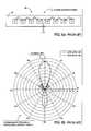
- the embodiment illustrated in FIG. 2comprises a grid pattern of 8 rows each containing 14 holes. The distance between each row is 3.5 millimeters. This results in a center frequency of approximately 24 GHz, which is desired for HRR applications.
- RF circuitscan be located on the rear side of the first substrate layer 31 . Some of these circuits can require a solid ground plane to work properly. This can prevent the openings from being etched on the ground plane 41 . In such instances, the openings can be etched on a metalized plane located on the top surface of the second substrate layer 33 on the bottom surface of the third (radome) layer 35 . While moving the openings off of the ground plane 41 will cause the performance of the antenna to be reduced, it allows the invention to be practiced in units that contain RF circuitry on the rear side of the first substrate layer 31 .
- FIG. 5 bshows the gain pattern simulated at 24 GHz for the antenna in accordance with the embodiment shown in FIG. 5 a .
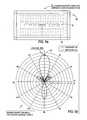
- FIG. 6 ashows a slot coupled microstrip array antenna 61 without periodic filters etched into the ground plane, with the corresponding gain pattern simulated at 24 GHz shown in FIG. 6 b .
- the periodic filtersincrease the gain of the antenna array.
- a computed gain 55 of 15.8 dBi for an antenna unit 50 in accordance with the present inventionis compared to a computed gain 65 of 13.8 dBi for an antenna unit 60 that does not have the periodic filters etched in the ground plane.
- an increase of about 2 dBiis obtained using holes etched in the ground plane in accordance with the present invention.
- the antenna unit in accordance with the present inventionsuppresses undesired surface waves associated with the uses of slot coupled microstrip antenna arrays by using periodic filters etched into the ground plan. By doing so, an increase in isolation between slot coupled microstrip antenna arrays.
- two slot coupled microstrip antenna arraysare separated by a distance of 40 millimeters and have a series of rows of filters etched between them, with each row containing 8 filters. Isolation between the antenna arrays (measured between 22 GHz and 26 GHz) was greater than ⁇ 30 dB for all frequencies within the measured range. It was measured at greater than ⁇ 40 dB for some frequencies within this range, and greater than ⁇ 50 dB for other frequencies within this range.
- increased gain of the slot coupled antenna arraysoccurs over the same frequency range.
Landscapes
- Physics & Mathematics (AREA)
- Electromagnetism (AREA)
- Waveguide Aerials (AREA)
- Variable-Direction Aerials And Aerial Arrays (AREA)
- Details Of Aerials (AREA)
- Aerials With Secondary Devices (AREA)
Abstract
Description
Claims (25)
Priority Applications (4)
| Application Number | Priority Date | Filing Date | Title |
|---|---|---|---|
| US10/289,874US6954177B2 (en) | 2002-11-07 | 2002-11-07 | Microstrip antenna array with periodic filters for enhanced performance |
| JP2003377945AJP4713823B2 (en) | 2002-11-07 | 2003-11-07 | Method for improving insulation between antenna unit and multiple microstrip antenna array |
| EP03257059AEP1418643B1 (en) | 2002-11-07 | 2003-11-07 | Microstrip antenna array with periodic filters |
| DE60325928TDE60325928D1 (en) | 2002-11-07 | 2003-11-07 | Microstrip array antenna with periodic filters |
Applications Claiming Priority (1)
| Application Number | Priority Date | Filing Date | Title |
|---|---|---|---|
| US10/289,874US6954177B2 (en) | 2002-11-07 | 2002-11-07 | Microstrip antenna array with periodic filters for enhanced performance |
Publications (2)
| Publication Number | Publication Date |
|---|---|
| US20040090368A1 US20040090368A1 (en) | 2004-05-13 |
| US6954177B2true US6954177B2 (en) | 2005-10-11 |
Family
ID=32107643
Family Applications (1)
| Application Number | Title | Priority Date | Filing Date |
|---|---|---|---|
| US10/289,874Expired - LifetimeUS6954177B2 (en) | 2002-11-07 | 2002-11-07 | Microstrip antenna array with periodic filters for enhanced performance |
Country Status (4)
| Country | Link |
|---|---|
| US (1) | US6954177B2 (en) |
| EP (1) | EP1418643B1 (en) |
| JP (1) | JP4713823B2 (en) |
| DE (1) | DE60325928D1 (en) |
Cited By (45)
| Publication number | Priority date | Publication date | Assignee | Title |
|---|---|---|---|---|
| US20060097917A1 (en)* | 2002-10-24 | 2006-05-11 | Marc Thevenot | Frequency multiband antenna with photonic bandgap material |
| US20060273975A1 (en)* | 2005-06-01 | 2006-12-07 | Accton Technology Corporation | Antenna structure |
| US20070285316A1 (en)* | 2006-06-13 | 2007-12-13 | Nokia Corporation | Antenna array and unit cell using an artificial magnetic layer |
| US20080094302A1 (en)* | 2006-10-20 | 2008-04-24 | Hong Kong Applied Science And Technology Research Institute Co., Ltd. | Systems and methods using ground plane filters for device isolation |
| US20080204347A1 (en)* | 2007-02-26 | 2008-08-28 | Alvey Graham R | Increasing isolation between multiple antennas with a grounded meander line structure |
| US20080265087A1 (en)* | 2007-04-27 | 2008-10-30 | Quinn Edward W | Power and imaging system for an airship |
| US20090002239A1 (en)* | 2007-06-28 | 2009-01-01 | Shau-Gang Mao | Micro-strip antenna with l-shaped band-stop filter |
| US7756059B1 (en) | 2008-05-19 | 2010-07-13 | Meru Networks | Differential signal-to-noise ratio based rate adaptation |
| US7808908B1 (en) | 2006-09-20 | 2010-10-05 | Meru Networks | Wireless rate adaptation |
| US7826426B1 (en) | 2005-12-05 | 2010-11-02 | Meru Networks | Seamless mobility in wireless networks |
| US20100295739A1 (en)* | 2009-05-21 | 2010-11-25 | Industrial Technology Research Institute | Radiation pattern insulator and multiple antennae system thereof and communication device using the multiple antennae system |
| US20110018083A1 (en)* | 2007-08-29 | 2011-01-27 | Sony Corporation | Method of producing semiconductor device, solid-state imaging device, method of producing electric apparatus, and electric apparatus |
| US7894436B1 (en) | 2007-09-07 | 2011-02-22 | Meru Networks | Flow inspection |
| US20110071761A1 (en)* | 2009-09-18 | 2011-03-24 | Charles Arnold Cummings | Holistic cybernetic vehicle control |
| US8010820B1 (en) | 2007-08-28 | 2011-08-30 | Meru Networks | Controlling multiple-radio wireless communication access points when using power over Ethernet |
| US8064601B1 (en) | 2006-03-31 | 2011-11-22 | Meru Networks | Security in wireless communication systems |
| US8081589B1 (en) | 2007-08-28 | 2011-12-20 | Meru Networks | Access points using power over ethernet |
| US8145136B1 (en) | 2007-09-25 | 2012-03-27 | Meru Networks | Wireless diagnostics |
| US8238834B1 (en) | 2008-09-11 | 2012-08-07 | Meru Networks | Diagnostic structure for wireless networks |
| US8284191B1 (en) | 2008-04-04 | 2012-10-09 | Meru Networks | Three-dimensional wireless virtual reality presentation |
| US8295177B1 (en) | 2007-09-07 | 2012-10-23 | Meru Networks | Flow classes |
| US8325753B1 (en) | 2008-06-10 | 2012-12-04 | Meru Networks | Selective suppression of 802.11 ACK frames |
| US8344953B1 (en) | 2008-05-13 | 2013-01-01 | Meru Networks | Omni-directional flexible antenna support panel |
| US8369794B1 (en) | 2008-06-18 | 2013-02-05 | Meru Networks | Adaptive carrier sensing and power control |
| US20130136853A1 (en)* | 2008-12-16 | 2013-05-30 | Lockheed Martin Corporation | Randomized circular grids for low-scatter em shielding of a sensor window |
| US8522353B1 (en) | 2007-08-15 | 2013-08-27 | Meru Networks | Blocking IEEE 802.11 wireless access |
| US8599734B1 (en) | 2008-09-30 | 2013-12-03 | Meru Networks | TCP proxy acknowledgements |
| US8799648B1 (en) | 2007-08-15 | 2014-08-05 | Meru Networks | Wireless network controller certification authority |
| US8893252B1 (en) | 2008-04-16 | 2014-11-18 | Meru Networks | Wireless communication selective barrier |
| US8941539B1 (en) | 2011-02-23 | 2015-01-27 | Meru Networks | Dual-stack dual-band MIMO antenna |
| US8981998B2 (en) | 2010-04-02 | 2015-03-17 | Furukawa Electric Co., Ltd. | Built-in transmitting and receiving integrated radar antenna |
| US9025581B2 (en) | 2005-12-05 | 2015-05-05 | Meru Networks | Hybrid virtual cell and virtual port wireless network architecture |
| US9142873B1 (en) | 2005-12-05 | 2015-09-22 | Meru Networks | Wireless communication antennae for concurrent communication in an access point |
| US9185618B1 (en) | 2005-12-05 | 2015-11-10 | Meru Networks | Seamless roaming in wireless networks |
| US9197482B1 (en) | 2009-12-29 | 2015-11-24 | Meru Networks | Optimizing quality of service in wireless networks |
| US9215754B2 (en) | 2007-03-07 | 2015-12-15 | Menu Networks | Wi-Fi virtual port uplink medium access control |
| US9215745B1 (en) | 2005-12-09 | 2015-12-15 | Meru Networks | Network-based control of stations in a wireless communication network |
| US20150364817A1 (en)* | 2013-01-28 | 2015-12-17 | Zte Corporation | Antenna system |
| US9794801B1 (en) | 2005-12-05 | 2017-10-17 | Fortinet, Inc. | Multicast and unicast messages in a virtual cell communication system |
| US9838911B1 (en) | 2007-08-20 | 2017-12-05 | Fortinet, Inc. | Multitier wireless data distribution |
| US9860813B2 (en) | 2005-12-05 | 2018-01-02 | Fortinet, Inc. | Seamless mobility in wireless networks |
| US9906650B2 (en) | 2011-06-26 | 2018-02-27 | Fortinet, Llc | Voice adaptation for wireless communication |
| US9917752B1 (en) | 2011-06-24 | 2018-03-13 | Fortinet, Llc | Optimization of contention paramaters for quality of service of VOIP (voice over internet protocol) calls in a wireless communication network |
| US10327186B2 (en) | 2005-12-05 | 2019-06-18 | Fortinet, Inc. | Aggregated beacons for per station control of multiple stations across multiple access points in a wireless communication network |
| US10326196B2 (en)* | 2014-09-25 | 2019-06-18 | Samsung Electronics Co., Ltd | Antenna device |
Families Citing this family (11)
| Publication number | Priority date | Publication date | Assignee | Title |
|---|---|---|---|---|
| DE10237790A1 (en)* | 2002-08-17 | 2004-02-26 | Robert Bosch Gmbh | System for detecting and displaying objects around vehicle, comprises transmitter and receiver for radiation in Giga region consisting of antenna enclosed in radome forming lens which concentrates and directs beam |
| US6943737B2 (en)* | 2003-08-27 | 2005-09-13 | The United States Of America As Represented By The Secretary Of The Navy | GPS microstrip antenna |
| US6867737B1 (en)* | 2003-08-27 | 2005-03-15 | The United States Of America As Represented By The Secretary Of The Navy | Reduced size GPS conical shaped microstrip antenna array |
| CN100384015C (en)* | 2005-05-30 | 2008-04-23 | 东南大学 | Balanced feed broadband substrate integrated waveguide slot array antenna unit |
| JP2007166115A (en)* | 2005-12-12 | 2007-06-28 | Matsushita Electric Ind Co Ltd | Antenna device |
| DE102008056729B3 (en)* | 2008-11-11 | 2010-05-12 | Kathrein-Werke Kg | RFID antenna system |
| US9293033B2 (en)* | 2013-07-16 | 2016-03-22 | The Boeing Company | Wireless fuel sensor system |
| US10141626B2 (en)* | 2014-07-23 | 2018-11-27 | Apple Inc. | Electronic device printed circuit board patch antenna |
| CN105789870B (en)* | 2016-03-07 | 2018-12-11 | 哈尔滨工业大学 | A kind of broadband low minor lobe micro-strip antenna array for anti-collision radar system |
| US10522891B2 (en)* | 2017-08-03 | 2019-12-31 | California Institute Of Technology | Millimeter-wave coupler for semi-confocal fabry-perot cavity |
| CN109449608B (en)* | 2018-12-05 | 2020-11-17 | 上海航天电子通讯设备研究所 | Microstrip array antenna structure capable of improving isolation degree between antennas |
Citations (11)
| Publication number | Priority date | Publication date | Assignee | Title |
|---|---|---|---|---|
| US4937972A (en) | 1989-03-16 | 1990-07-03 | Freitus Joseph P | Self-contained plant growth system |
| US5045862A (en)* | 1988-12-28 | 1991-09-03 | Her Majesty The Queen In Right Of Canada, As Represented By The Minister Of Communications | Dual polarization microstrip array antenna |
| US5068669A (en)* | 1988-09-01 | 1991-11-26 | Apti, Inc. | Power beaming system |
| US5448249A (en)* | 1992-02-27 | 1995-09-05 | Murata Manufacturing Co., Ltd. | Antenna device |
| US5896104A (en) | 1991-09-04 | 1999-04-20 | Honda Giken Kogyo Kabushiki Kaisha | FM radar system |
| US5912645A (en)* | 1996-03-19 | 1999-06-15 | Her Majesty The Queen In Right Of Canada, As Represented By The Minister Of Industry Through The Communications Research Centre | Array feed for axially symmetric and offset reflectors |
| US6313797B1 (en)* | 1998-10-22 | 2001-11-06 | Murata Manufacturing Co., Ltd. | Dielectric antenna including filter, dielectric antenna including duplexer, and radio apparatus |
| US6466172B1 (en)* | 2001-10-19 | 2002-10-15 | The United States Of America As Represented By The Secretary Of The Navy | GPS and telemetry antenna for use on projectiles |
| US6529092B2 (en)* | 2000-08-30 | 2003-03-04 | Kabushiki Kaisha Toshiba | Superconductor filter and radio transmitter-receiver |
| US6630907B1 (en)* | 2002-07-03 | 2003-10-07 | The United States Of America As Represented By The Secretary Of The Navy | Broadband telemetry antenna having an integrated filter |
| US6774867B2 (en)* | 2000-10-04 | 2004-08-10 | E-Tenna Corporation | Multi-resonant, high-impedance electromagnetic surfaces |
Family Cites Families (6)
| Publication number | Priority date | Publication date | Assignee | Title |
|---|---|---|---|---|
| JPS6489602A (en)* | 1987-09-30 | 1989-04-04 | Nec Corp | Printed antenna |
| US4973972A (en)* | 1989-09-07 | 1990-11-27 | The United States Of America As Represented By The Administrator Of The National Aeronautics And Space Adminstration | Stripline feed for a microstrip array of patch elements with teardrop shaped probes |
| JPH10200326A (en)* | 1997-01-07 | 1998-07-31 | Mitsubishi Electric Corp | Antenna device |
| JP2894325B2 (en)* | 1997-06-25 | 1999-05-24 | 日本電気株式会社 | Electronic circuit shield structure |
| JP3650957B2 (en)* | 1999-07-13 | 2005-05-25 | 株式会社村田製作所 | Transmission line, filter, duplexer and communication device |
| JP2001111328A (en)* | 1999-10-06 | 2001-04-20 | Mitsubishi Electric Corp | Microstrip antenna and design method thereof |
- 2002
- 2002-11-07USUS10/289,874patent/US6954177B2/ennot_activeExpired - Lifetime
- 2003
- 2003-11-07JPJP2003377945Apatent/JP4713823B2/ennot_activeExpired - Lifetime
- 2003-11-07EPEP03257059Apatent/EP1418643B1/ennot_activeExpired - Lifetime
- 2003-11-07DEDE60325928Tpatent/DE60325928D1/ennot_activeExpired - Lifetime
Patent Citations (11)
| Publication number | Priority date | Publication date | Assignee | Title |
|---|---|---|---|---|
| US5068669A (en)* | 1988-09-01 | 1991-11-26 | Apti, Inc. | Power beaming system |
| US5045862A (en)* | 1988-12-28 | 1991-09-03 | Her Majesty The Queen In Right Of Canada, As Represented By The Minister Of Communications | Dual polarization microstrip array antenna |
| US4937972A (en) | 1989-03-16 | 1990-07-03 | Freitus Joseph P | Self-contained plant growth system |
| US5896104A (en) | 1991-09-04 | 1999-04-20 | Honda Giken Kogyo Kabushiki Kaisha | FM radar system |
| US5448249A (en)* | 1992-02-27 | 1995-09-05 | Murata Manufacturing Co., Ltd. | Antenna device |
| US5912645A (en)* | 1996-03-19 | 1999-06-15 | Her Majesty The Queen In Right Of Canada, As Represented By The Minister Of Industry Through The Communications Research Centre | Array feed for axially symmetric and offset reflectors |
| US6313797B1 (en)* | 1998-10-22 | 2001-11-06 | Murata Manufacturing Co., Ltd. | Dielectric antenna including filter, dielectric antenna including duplexer, and radio apparatus |
| US6529092B2 (en)* | 2000-08-30 | 2003-03-04 | Kabushiki Kaisha Toshiba | Superconductor filter and radio transmitter-receiver |
| US6774867B2 (en)* | 2000-10-04 | 2004-08-10 | E-Tenna Corporation | Multi-resonant, high-impedance electromagnetic surfaces |
| US6466172B1 (en)* | 2001-10-19 | 2002-10-15 | The United States Of America As Represented By The Secretary Of The Navy | GPS and telemetry antenna for use on projectiles |
| US6630907B1 (en)* | 2002-07-03 | 2003-10-07 | The United States Of America As Represented By The Secretary Of The Navy | Broadband telemetry antenna having an integrated filter |
Non-Patent Citations (7)
| Title |
|---|
| Dan Sievepiper, Member, IEEE, Lijun Zhang, Romulo F. Jimenez Broas, Nicholas G. Alexopolous, Fellow, IEEE, and Eli Yablonovitch, Fellow, IEEE High-Impedance Electromagnetic Surfaces with a Forbidden Frequency Band, IEEE Transactions on Microwave Theory and Techniques, vol. 47, No. 11, Nov., 1999. |
| Fan Yang et al: Mutual Coupling Reduction Of Microstrip Antennas Using Electromagnetic Band-Gap Structure, IEEE Antennas And Propagation Society International Symposium, 2001 Digest, APS. Boston, MA, Jul. 8-13, 2001, pp. 478-481, XPO10564130. |
| Lee Y et al: Institute of Electrical And Electronics Engineers: "Multi-Layer Spatial Angular Filter With Air Gap Tuner To Suppress The Grating Lobes Of Microstrip Patch Arrays" Jun. 2-7, 2002, pp. 1329-1332, XPOO11100006. |
| Leong, K M K H et al: "Coupling Suppression In Microstrip Lines Using A Bi-Periodically Perforated Ground Plane", May 5, 2002, pp. 169-171, XPOO1114925. |
| Marc Thevenot, Cyril Cheype, Alain Reineix, and Bernard Jecko, Member IEEE, Directive Photonic-Bandgap Antennas, IEEE Transactions on Microwave Theory and Techniques, vol. 47, No. 11, Nov., 1999. |
| Ramon Gonzalo, Student Member, IEEE, Peter De Maagt, Member, IEEE and Mario Sorolla, Member, IEEE, Enhanced Patch-Antenna Performance by Suppressing Surface Waves Using Photonic-Bandgap Substrates, IEEE Transactions on Microwave Theory and Techniques, vol. 47, No. 11, Nov., 1999. |
| Vesna Radisic, Student Member, IEEE, Yongxi, Member, IEEE, Roberto Coccioli, Member, IEEE, and Tatsuo Itoh, Life Fellow, IEEE, Novel 2-D Photonic Bandgap Structure for Microstrip Lines, IEEE Microwave and Guided Wave Letters, vol. 8, No. 2, Feb., 1998. |
Cited By (67)
| Publication number | Priority date | Publication date | Assignee | Title |
|---|---|---|---|---|
| US20060097917A1 (en)* | 2002-10-24 | 2006-05-11 | Marc Thevenot | Frequency multiband antenna with photonic bandgap material |
| US7411564B2 (en)* | 2002-10-24 | 2008-08-12 | Centre National De La Recherche Scientifique (C.N.R.S.) | Frequency multiband antenna with photonic bandgap material |
| US7365684B2 (en)* | 2005-06-01 | 2008-04-29 | Accton Technology Corporation | Antenna having a filter and a signal feed-in point |
| US20060273975A1 (en)* | 2005-06-01 | 2006-12-07 | Accton Technology Corporation | Antenna structure |
| US9860813B2 (en) | 2005-12-05 | 2018-01-02 | Fortinet, Inc. | Seamless mobility in wireless networks |
| US8160664B1 (en) | 2005-12-05 | 2012-04-17 | Meru Networks | Omni-directional antenna supporting simultaneous transmission and reception of multiple radios with narrow frequency separation |
| US9761958B2 (en) | 2005-12-05 | 2017-09-12 | Fortinet, Inc. | Wireless communication antennae for concurrent communication in an access point |
| US9794801B1 (en) | 2005-12-05 | 2017-10-17 | Fortinet, Inc. | Multicast and unicast messages in a virtual cell communication system |
| US9025581B2 (en) | 2005-12-05 | 2015-05-05 | Meru Networks | Hybrid virtual cell and virtual port wireless network architecture |
| US9185618B1 (en) | 2005-12-05 | 2015-11-10 | Meru Networks | Seamless roaming in wireless networks |
| US10225764B2 (en) | 2005-12-05 | 2019-03-05 | Fortinet, Inc. | Per user uplink medium access control on a Wi-Fi communication network |
| US8787309B1 (en) | 2005-12-05 | 2014-07-22 | Meru Networks | Seamless mobility in wireless networks |
| US9930595B2 (en) | 2005-12-05 | 2018-03-27 | Fortinet, Inc. | Seamless roaming in wireless networks |
| US10278105B2 (en) | 2005-12-05 | 2019-04-30 | Fortinet, Inc. | Seamless mobility in wireless networks |
| US9142873B1 (en) | 2005-12-05 | 2015-09-22 | Meru Networks | Wireless communication antennae for concurrent communication in an access point |
| US7826426B1 (en) | 2005-12-05 | 2010-11-02 | Meru Networks | Seamless mobility in wireless networks |
| US10327186B2 (en) | 2005-12-05 | 2019-06-18 | Fortinet, Inc. | Aggregated beacons for per station control of multiple stations across multiple access points in a wireless communication network |
| US9215745B1 (en) | 2005-12-09 | 2015-12-15 | Meru Networks | Network-based control of stations in a wireless communication network |
| US8867744B1 (en) | 2006-03-31 | 2014-10-21 | Meru Networks | Security in wireless communication systems |
| US8064601B1 (en) | 2006-03-31 | 2011-11-22 | Meru Networks | Security in wireless communication systems |
| US20070285316A1 (en)* | 2006-06-13 | 2007-12-13 | Nokia Corporation | Antenna array and unit cell using an artificial magnetic layer |
| US7471247B2 (en)* | 2006-06-13 | 2008-12-30 | Nokia Siemens Networks, Oy | Antenna array and unit cell using an artificial magnetic layer |
| US7808908B1 (en) | 2006-09-20 | 2010-10-05 | Meru Networks | Wireless rate adaptation |
| US8767548B1 (en) | 2006-09-20 | 2014-07-01 | Meru Networks | Wireless rate adaptation |
| US7629930B2 (en)* | 2006-10-20 | 2009-12-08 | Hong Kong Applied Science And Technology Research Institute Co., Ltd. | Systems and methods using ground plane filters for device isolation |
| US20080094302A1 (en)* | 2006-10-20 | 2008-04-24 | Hong Kong Applied Science And Technology Research Institute Co., Ltd. | Systems and methods using ground plane filters for device isolation |
| US7701395B2 (en) | 2007-02-26 | 2010-04-20 | The Board Of Trustees Of The University Of Illinois | Increasing isolation between multiple antennas with a grounded meander line structure |
| US20080204347A1 (en)* | 2007-02-26 | 2008-08-28 | Alvey Graham R | Increasing isolation between multiple antennas with a grounded meander line structure |
| US9215754B2 (en) | 2007-03-07 | 2015-12-15 | Menu Networks | Wi-Fi virtual port uplink medium access control |
| US7744032B2 (en)* | 2007-04-27 | 2010-06-29 | Lockheed Martin Corporation | Power and imaging system for an airship |
| US20080265087A1 (en)* | 2007-04-27 | 2008-10-30 | Quinn Edward W | Power and imaging system for an airship |
| US7889136B2 (en)* | 2007-06-28 | 2011-02-15 | Richwave Technology Corp. | Micro-strip antenna with L-shaped band-stop filter |
| US20090002239A1 (en)* | 2007-06-28 | 2009-01-01 | Shau-Gang Mao | Micro-strip antenna with l-shaped band-stop filter |
| US8522353B1 (en) | 2007-08-15 | 2013-08-27 | Meru Networks | Blocking IEEE 802.11 wireless access |
| US8799648B1 (en) | 2007-08-15 | 2014-08-05 | Meru Networks | Wireless network controller certification authority |
| US9838911B1 (en) | 2007-08-20 | 2017-12-05 | Fortinet, Inc. | Multitier wireless data distribution |
| US10341920B2 (en) | 2007-08-20 | 2019-07-02 | Fortinet, Inc | Multitier wireless data distribution |
| US8081589B1 (en) | 2007-08-28 | 2011-12-20 | Meru Networks | Access points using power over ethernet |
| US8010820B1 (en) | 2007-08-28 | 2011-08-30 | Meru Networks | Controlling multiple-radio wireless communication access points when using power over Ethernet |
| US20110018083A1 (en)* | 2007-08-29 | 2011-01-27 | Sony Corporation | Method of producing semiconductor device, solid-state imaging device, method of producing electric apparatus, and electric apparatus |
| US7894436B1 (en) | 2007-09-07 | 2011-02-22 | Meru Networks | Flow inspection |
| US8995459B1 (en) | 2007-09-07 | 2015-03-31 | Meru Networks | Recognizing application protocols by identifying message traffic patterns |
| US8295177B1 (en) | 2007-09-07 | 2012-10-23 | Meru Networks | Flow classes |
| US8145136B1 (en) | 2007-09-25 | 2012-03-27 | Meru Networks | Wireless diagnostics |
| US8284191B1 (en) | 2008-04-04 | 2012-10-09 | Meru Networks | Three-dimensional wireless virtual reality presentation |
| US8893252B1 (en) | 2008-04-16 | 2014-11-18 | Meru Networks | Wireless communication selective barrier |
| US8344953B1 (en) | 2008-05-13 | 2013-01-01 | Meru Networks | Omni-directional flexible antenna support panel |
| US7756059B1 (en) | 2008-05-19 | 2010-07-13 | Meru Networks | Differential signal-to-noise ratio based rate adaptation |
| US8958334B2 (en) | 2008-05-19 | 2015-02-17 | Meru Networks | Differential signal-to-noise ratio based rate adaptation |
| US8456993B1 (en) | 2008-05-19 | 2013-06-04 | Meru Networks | Differential signal-to-noise ratio based rate adaptation |
| US8325753B1 (en) | 2008-06-10 | 2012-12-04 | Meru Networks | Selective suppression of 802.11 ACK frames |
| US8369794B1 (en) | 2008-06-18 | 2013-02-05 | Meru Networks | Adaptive carrier sensing and power control |
| US8238834B1 (en) | 2008-09-11 | 2012-08-07 | Meru Networks | Diagnostic structure for wireless networks |
| US8599734B1 (en) | 2008-09-30 | 2013-12-03 | Meru Networks | TCP proxy acknowledgements |
| US20130136853A1 (en)* | 2008-12-16 | 2013-05-30 | Lockheed Martin Corporation | Randomized circular grids for low-scatter em shielding of a sensor window |
| US9073084B2 (en)* | 2008-12-16 | 2015-07-07 | Lockheed Martin Corporation | Method for electromagnetically shielding a sensor window |
| US20100295739A1 (en)* | 2009-05-21 | 2010-11-25 | Industrial Technology Research Institute | Radiation pattern insulator and multiple antennae system thereof and communication device using the multiple antennae system |
| US8643546B2 (en) | 2009-05-21 | 2014-02-04 | Industrial Technology Research Institute | Radiation pattern insulator and multiple antennae system thereof and communication device using the multiple antennae system |
| US8731815B2 (en) | 2009-09-18 | 2014-05-20 | Charles Arnold Cummings | Holistic cybernetic vehicle control |
| US20110071761A1 (en)* | 2009-09-18 | 2011-03-24 | Charles Arnold Cummings | Holistic cybernetic vehicle control |
| US9197482B1 (en) | 2009-12-29 | 2015-11-24 | Meru Networks | Optimizing quality of service in wireless networks |
| US8981998B2 (en) | 2010-04-02 | 2015-03-17 | Furukawa Electric Co., Ltd. | Built-in transmitting and receiving integrated radar antenna |
| US8941539B1 (en) | 2011-02-23 | 2015-01-27 | Meru Networks | Dual-stack dual-band MIMO antenna |
| US9917752B1 (en) | 2011-06-24 | 2018-03-13 | Fortinet, Llc | Optimization of contention paramaters for quality of service of VOIP (voice over internet protocol) calls in a wireless communication network |
| US9906650B2 (en) | 2011-06-26 | 2018-02-27 | Fortinet, Llc | Voice adaptation for wireless communication |
| US20150364817A1 (en)* | 2013-01-28 | 2015-12-17 | Zte Corporation | Antenna system |
| US10326196B2 (en)* | 2014-09-25 | 2019-06-18 | Samsung Electronics Co., Ltd | Antenna device |
Also Published As
| Publication number | Publication date |
|---|---|
| EP1418643B1 (en) | 2009-01-21 |
| EP1418643A3 (en) | 2004-09-15 |
| DE60325928D1 (en) | 2009-03-12 |
| EP1418643A2 (en) | 2004-05-12 |
| JP4713823B2 (en) | 2011-06-29 |
| US20040090368A1 (en) | 2004-05-13 |
| JP2004159341A (en) | 2004-06-03 |
Similar Documents
| Publication | Publication Date | Title |
|---|---|---|
| US6954177B2 (en) | Microstrip antenna array with periodic filters for enhanced performance | |
| KR101621480B1 (en) | Transit structure of waveguide and dielectric waveguide | |
| EP0642190B1 (en) | Built-in radiation structure for a millimeter wave radar sensor | |
| US12009591B2 (en) | Electromagnetic band gap structure (EBG) | |
| US11133594B2 (en) | System and method with multilayer laminated waveguide antenna | |
| US9323877B2 (en) | Beam-steered wide bandwidth electromagnetic band gap antenna | |
| US6008770A (en) | Planar antenna and antenna array | |
| US8022861B2 (en) | Dual-band antenna array and RF front-end for mm-wave imager and radar | |
| KR101518429B1 (en) | Antenna array for ultra wide band radar applications | |
| US8786496B2 (en) | Three-dimensional array antenna on a substrate with enhanced backlobe suppression for mm-wave automotive applications | |
| JP4217713B2 (en) | Antenna equipment for radar applications in automobiles, for example | |
| CN111755819B (en) | Inverted microstrip traveling wave patch array antenna system | |
| US20100188309A1 (en) | Radar antenna | |
| CN111755832B (en) | Integrated back cavity slot array antenna system | |
| WO2015012942A1 (en) | Polarization dependent electromagnetic bandgap antenna and related methods | |
| US10756446B2 (en) | Planar antenna structure with reduced coupling between antenna arrays | |
| JP2004516734A (en) | Antenna device | |
| CN110828978B (en) | 77GHz vehicle-mounted radar low-sidelobe microstrip array antenna with shielding cover | |
| CN115149249A (en) | High-Gain Microstrip Antenna Array, Millimeter-Wave Vehicle Radar Sensor and Vehicle | |
| CN112912753A (en) | Radar sensor | |
| CN113394560B (en) | Antenna assembly, antenna device and movable platform | |
| US6999030B1 (en) | Linear polarization planar microstrip antenna array with circular patch elements and co-planar annular sector parasitic strips | |
| CN115395213B (en) | Antenna unit, array antenna, radar sensor and electronic equipment | |
| Naseh et al. | Miniaturized siw-cbs planar tx/rx antenna arrays for microwave cw/fmcw doppler radars | |
| JP2017003328A (en) | Radar device |
Legal Events
| Date | Code | Title | Description |
|---|---|---|---|
| AS | Assignment | Owner name:M/A-COM, INC., MASSACHUSETTS Free format text:ASSIGNMENT OF ASSIGNORS INTEREST;ASSIGNORS:CHANNABASAPPA, ESWARAPPA;KOLAK, FRANK;ANDERSON, RICHARD ALAN;REEL/FRAME:013472/0925 Effective date:20021107 | |
| STCF | Information on status: patent grant | Free format text:PATENTED CASE | |
| AS | Assignment | Owner name:AUTOILV ASP, INC., UTAH Free format text:ASSIGNMENT OF ASSIGNORS INTEREST;ASSIGNORS:M/A-COM, INC.;TYCO ELECTRONICS TECHNOLOGY RESOURCES, INC.;TYCO ELECTRONICS CORPORATION;AND OTHERS;REEL/FRAME:021750/0045 Effective date:20080926 Owner name:AUTOILV ASP, INC.,UTAH Free format text:ASSIGNMENT OF ASSIGNORS INTEREST;ASSIGNORS:M/A-COM, INC.;TYCO ELECTRONICS TECHNOLOGY RESOURCES, INC.;TYCO ELECTRONICS CORPORATION;AND OTHERS;REEL/FRAME:021750/0045 Effective date:20080926 | |
| FPAY | Fee payment | Year of fee payment:4 | |
| FPAY | Fee payment | Year of fee payment:8 | |
| FPAY | Fee payment | Year of fee payment:12 | |
| AS | Assignment | Owner name:VEONEER US, INC., MICHIGAN Free format text:ASSIGNMENT OF ASSIGNORS INTEREST;ASSIGNOR:AUTOLIV ASP, INC.;REEL/FRAME:046326/0137 Effective date:20180608 | |
| AS | Assignment | Owner name:VEONEER US, LLC, DELAWARE Free format text:CHANGE OF NAME;ASSIGNOR:VEONEER US, INC.;REEL/FRAME:061069/0535 Effective date:20220401 | |
| AS | Assignment | Owner name:VEONEER US, LLC, MICHIGAN Free format text:AFFIDAVIT / CHANGE OF ADDRESS;ASSIGNOR:VEONEER US, LLC;REEL/FRAME:065049/0150 Effective date:20220426 |