US6952812B2 - Design analysis tool for path extraction and false path identification and method thereof - Google Patents
Design analysis tool for path extraction and false path identification and method thereofDownload PDFInfo
- Publication number
- US6952812B2 US6952812B2US09/781,492US78149201AUS6952812B2US 6952812 B2US6952812 B2US 6952812B2US 78149201 AUS78149201 AUS 78149201AUS 6952812 B2US6952812 B2US 6952812B2
- Authority
- US
- United States
- Prior art keywords
- path
- conditions
- paths
- satisfied
- false
- Prior art date
- Legal status (The legal status is an assumption and is not a legal conclusion. Google has not performed a legal analysis and makes no representation as to the accuracy of the status listed.)
- Expired - Fee Related, expires
Links
Images


Classifications
- G—PHYSICS
- G01—MEASURING; TESTING
- G01R—MEASURING ELECTRIC VARIABLES; MEASURING MAGNETIC VARIABLES
- G01R31/00—Arrangements for testing electric properties; Arrangements for locating electric faults; Arrangements for electrical testing characterised by what is being tested not provided for elsewhere
- G01R31/28—Testing of electronic circuits, e.g. by signal tracer
- G01R31/317—Testing of digital circuits
- G01R31/3181—Functional testing
- G01R31/3183—Generation of test inputs, e.g. test vectors, patterns or sequences
- G01R31/318342—Generation of test inputs, e.g. test vectors, patterns or sequences by preliminary fault modelling, e.g. analysis, simulation
- G01R31/318357—Simulation
- G—PHYSICS
- G06—COMPUTING OR CALCULATING; COUNTING
- G06F—ELECTRIC DIGITAL DATA PROCESSING
- G06F30/00—Computer-aided design [CAD]
- G06F30/30—Circuit design
- G06F30/32—Circuit design at the digital level
- G06F30/33—Design verification, e.g. functional simulation or model checking
- G06F30/3308—Design verification, e.g. functional simulation or model checking using simulation
- G06F30/3312—Timing analysis
- G—PHYSICS
- G01—MEASURING; TESTING
- G01R—MEASURING ELECTRIC VARIABLES; MEASURING MAGNETIC VARIABLES
- G01R31/00—Arrangements for testing electric properties; Arrangements for locating electric faults; Arrangements for electrical testing characterised by what is being tested not provided for elsewhere
- G01R31/28—Testing of electronic circuits, e.g. by signal tracer
- G01R31/317—Testing of digital circuits
- G01R31/3181—Functional testing
- G01R31/3183—Generation of test inputs, e.g. test vectors, patterns or sequences
- G01R31/318328—Generation of test inputs, e.g. test vectors, patterns or sequences for delay tests
Definitions
- This inventiongenerally relates to design analysis tools and more particularly to design analysis tools for performing timing analysis and identification of critical paths in electronic circuits.
- Static timing analysisplays an important role in defining circuit performance for today's high-speed integrated circuits.
- Static timing analysis toolsidentify all the structural paths in the design and the calculated delay along each one of these paths.
- the term ‘path’refers to two nodes in a circuit design coupled by one or more circuit devices. Typically, these paths start at a latch point and end at another latch point in the design. These paths are sorted according to their delay and the slowest (critical) paths in the design are identified. The designer then would have to work on these paths and try to optimize them to reduce the delay along these long paths in order to meet target performance frequency goals.
- the static timing analysis toolsare “true paths” because these paths cannot be activated in the design with various constraints.
- FIG. 1Illustrated in FIG. 1 , in block diagram form, is an exemplary path in a complex design.
- FIG. 2Illustrated in FIG. 2 , in partial logic diagram form, are examples of false paths.
- Illustrated in FIG. 3is a process flow for performing timing analysis and false path identification in conjunction with an automated test pattern generation tool.
- FIG. 4Illustrated in FIG. 4 , in block diagram form, is an example of path extraction and enumeration from a launch point to a capture point.
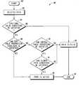
- FIG. 5Illustrated in FIG. 5 is a flow chart of false path identification in accordance with one embodiment of the present invention.
- FIG. 6Illustrated in FIG. 6 , in partial logic diagram form, is an example of false path identification between a launch point and a capture point in accordance with the present invention.
- FIG. 7Illustrated in FIG. 7 , in logic diagram form, is an example of the slow path condition of the flow chart of FIG. 5 .
- FIG. 1Illustrated in FIG. 1 is an integrated circuit portion 10 of a circuit design having a signal point represented as a launch point connected to an input of a block of custom logic 12 .
- Custom logic 12is formed of a plurality of transistors.
- An output of custom logic 12is connected to an input of synthesized logic gates block 14 .
- An output of synthesized logic gate block 14is coupled to an input of custom logic block 16 which is formed of a plurality of transistors.
- Intervening circuitrymay or may not be present between synthesized logic gates block 14 and custom logic block 16 as indicated by the broken line.
- An output of custom logic block 16provides an output capture point.
- integrated circuit portion 10illustrates a path corresponding to a circuit design in an integrated circuit in which a signal transition at the launch point results in an output transition at the output capture point.
- the timing analysis toolwill identify such paths in the design and will estimate the delay from when the transition occurs at the launch point and when it will appear at the output capture point.
- the purpose of timing analysisis to make sure that the delay of all the paths in the design fall below a certain timing budget which determines the speed of the circuit. If one of these paths exceeds the budget, then the designer will have to try and reduce the delay along that path in order to meet the timing budget.
- the pathsmay go through various different types of blocks.
- FIG. 2Illustrated in FIG. 2 is an example 20 of a portion of an integrated circuit.
- the integrated circuithas a plurality of latch circuits 22 , 24 , 26 and 28 .
- Each of the latch circuits 22 , 24 , 26 and 28has an input and an output for data. It should be well understood that the latch circuits described herein have both clock and data inputs.
- An output of latch circuit 22is connected to a first input of an AND gate 30 and to a first input of an AND gate 32 .
- An output of latch circuit 24is connected to a second input of an AND gate 32
- an output of latch circuit 26is connected to a first input of an AND gate 34 .
- An output of latch circuit 28is connected to a second input of AND gate 34 .
- the output of latch circuit 26is also connected to a second input of AND gate 30 .
- the output of AND gate 30is connected to an input of an inverter 36 .
- the output of AND gate 32is connected to a first input of an OR gate 40 .
- the output of AND gate 34is connected to a second input of OR gate 40 and the output of latch circuit 28 is connected to a third input of OR gate 40 .
- the output of inverter 36is connected to an input of inverter 38 having an output connected to an input of a latch circuit 42 .
- the output of OR gate 40is connected to an input of a latch circuit 44 .
- Latch circuits 42 and 44each have an output connected to surrounding logic 46 .
- the inputs of latch circuits 22 , 24 , 26 and 28are connected to surrounding logic 48 .
- the paths contained within the blockcan be false due to local constraints of the blocks themselves or due to external environmental constraints imposed by the surrounding logic.
- the path that starts at latch circuit 26 going into AND gate 34 on through OR gate 40 and going out to latch element 44is a false path because, in order to activate this path, the second input to AND gate 34 will have to be at the value 1 and the side input of the OR gate 40 will have to be at the value 0.
- This signal conditionis impossible because both signals are driven from the output of latch circuit 28 as shown in FIG. 2 .
- the Path P 1is false.
- the output of AND gate 30may possibly assume a logic one value should both inputs momentarily in the second time frame become a logic one as a result of such factors. Therefore, for a high-to-low signal transition at the output of latch 26 , the final value condition and the side value condition are both satisfied for path P 2 . But when a low-to-high logic transition is present at the output of latch 26 , the final value condition of the timing path going through AND gate 30 is violated because during the second time frame the second input of AND gate 30 is a controlling value (0) due to the one-hot constraint. This is an example of an external constraint from the surrounding logic that will make the path false. The following discussion is restricted to an analysis of local constraints imposed by the combinational blocks that contain the path and will not consider external constraints.
- a timing characterization step 52is initially performed on all the building blocks of the integrated circuit. It should be understood that the term “building blocks” encompasses both library cells and custom designed blocks.
- the output of the timing characterizationis provided to a timing analyzer for a timing analysis step 54 .
- the timing analysis step 54may be performed by any one of a variety of commercially existing or customized timing analysis tools.
- Information from the timing analysis step 54is provided to a path extraction and translation step 56 .
- an output of step 56is provided in the form of a false path identification step 58 .
- a false path reportis provided as an output of step 58 .
- the false path reportis provided back to the timing analysis tool and can be used in consecutive timing analysis step 54 .
- Intermediate results from the false path identification step 58are provided to an automated test pattern generation (ATPG) tool to check the satisfiability of logic values of nodes in the path or paths under consideration.
- the ATPG tooluses the intermediate results from false path identification step 58 and provides circuit and path information that is used to generate the false path report.
- ATPGsare well known in the art and are commercially available for performing specific test pattern generation on integrated circuits in an automated fashion to test their functionality.
- ATPG toolsperform a justifiability analysis by determining whether certain conditions can be satisfied or not. For example, ATPG tools may assign logic values to internal nets (circuit nodes) and analyze whether certain input value assignments can satisfy the assigned values.
- the justifiability function of ATPG toolsmay be implemented by various algorithms, including but not limited to the standard backtracking algorithm.
- steps 58 and 59are bidirectional.
- the bi-directionalityindicates that the false path identification process utilizes specific information from the ATPG and frequently calls for information or results created by the ATPG in order to perform the false path identification. Details of the interaction between the false path identification step 58 and an ATPG will be provided below.
- FIG. 4is an example of a complex path 60 that is identified by the timing analysis step 54 .
- the complex pathis identified as starting with a launch point having an input to a single path logic block 62 .
- An output of single path logic block 62is connected to an input of a multiple-path component logic block 63 .
- An output of multiple-path component logic block 63is connected to an input of a multiple-path component logic block 64 .
- An output of the multiple-path component logic block 64provides a capture point for the complex path.
- the timing analysis of step 54 in FIG. 3recognized only the inputs and outputs of single path component logic block 62 and multiple-path component logic blocks 63 and 64 .
- multiple-path component logic block 63comprises a plurality of component paths in the form of three separate paths.
- a first pathis connected to the input of multiple-path component logic block 63 and contains single path component logic block 66 .
- a second path of multiple-path component logic block 63contains a single path component logic block 67 and a single path component logic block 68 .
- Yet a third path of multiple-path component logic block 63contains a single path component logic block 69 and a single path component logic block 70 .
- multiple-path component logic block 64has two paths.
- a first pathcontains a single path component logic block 72 and a single path component logic block 73 .
- a second path of multiple-path component logic block 64contains a single path component logic block 74 .
- the single-path components and multiple-path componentsare formed using conventional combinational logic elements.
- the timing analysis toolidentifies the complex path going through blocks 62 , 63 and 64 as a single component timing path.
- the format of paths extracted by the timing analysis toolis very different from the format of paths that can be analyzed using ATPG.
- a start step 82transitions to receiving a selected path in step 84 .
- the selected pathis the result of the timing analysis step 54 and path extraction and translation step 56 of FIG. 3 .
- Path Pis characterized by the set of nodes along the path. Each one of these nodes will assume a certain transition that will require going from a previous value or initial value to a final value.
- condition 86In the next step of the process, we examine condition 86 .
- the conditionis a determination as to whether a set of final value conditions along all the nodes of the path can be satisfied within the combinational block or not.
- step 88we determine or evaluate whether a set of side value propagation conditions are satisfied. That condition states that all the side inputs of all the gates along the path have to assume non-controlling values.
- a non-controlling value for AND gates and NAND gatesis 1.
- a non-controlling value for OR gates and NOR gatesis 0.
- a non-controlling value for XOR gatescan be either 0 or 1.
- Step 88calls the ATPG tool to check whether these side-value propagation conditions can be satisfied by the circuit or not. If that is found to be true, then the path is determined to be an active path and we exit again at step 98 . If it is false, then we proceed to step 90 .
- the ATPGis called to check whether a set of initial value conditions of all the nodes along the paths is satisfied. If that is true, then we continue to step 92 where we determine whether a set of slower path conditions are satisfied. If so, the path is then characterized as being active in step 96 .
- An active characterizationmeans that the path could be true, but it could also be false for other reasons not being analyzed. Therefore, the term “active” is used rather than “true” or “false”.
- step 92If the result of step 92 is negative, then we determine that the path must be false in step 94 and we again exit at step 98 . If the initial value condition is true, we go to step 92 where we check for whether there are slower path conditions and whether any slower path conditions can be satisfied or not. A slower path condition requires that a slower path must exist at each side input where the side input propagation condition is violated. This condition will be explained below in FIG. 7 . If the condition of step 92 is found to be false, then the path is also determined to be false and we exit. Otherwise, if the condition is true, the path is determined to be an active path and we also exit. That terminates the process 80 for false path identification.
- a latch 102stores a digital value for the launch point.
- An output of latch 102is connected to a first input of an AND gate 104 .
- a second input 118 of AND gate 104is provided by combinational logic 114 .
- a third input 120 of AND gate 104is also provided by combinational logic 114 .
- An output of AND gate 104is connected to a first input of OR gate 106 .
- Combinational logic 114provides a second input 124 to OR gate 106 .
- An output of OR gate 106is connected to a first input of NAND gate 108 .
- Combinational logic 114provides a second input 128 to NAND gate 108 .
- NAND gate 108An output of NAND gate 108 is connected to a first input of exclusive OR (XOR) gate 110 .
- Combinational logic 114provides a second input 132 to XOR gate 110 .
- An output 134 of XOR gate 110is connected to a latch 112 that captures the digital value of the signal path example 100 .
- Also illustrated in FIG. 6is a sample signal transition from a digital 1 value to a digital 0 value at the output of latch 102 . The transition occurs after a first time period or time frame and transitions to a logic 0 value during a second time period or time frame.
- the transition at the input of AND gate 104is propagated through AND gate 104 , OR gate 106 , NAND gate 108 and XOR gate 110 .
- the path in FIG. 6goes through gates 104 , 106 , 108 and 110 .
- the set of the final value condition for the pathconsist of the following condition: having a 0 on input 116 , a 0 on input 122 , a 0 on input 126 , a 1 on input 130 , and a 1 on input 134 . These five signal conditions together define the final value condition for the path. This is the condition that will be checked during step 86 in FIG.
- step 88the side value propagation condition will be checked.
- the side value conditionhas the following: signal 118 at value 1, signal 120 at value 1, signal 124 at value 0, signal 128 at value 1, and signal 132 at value 0. Note here that since the signal transition at the input of XOR gate 110 is the same as the signal transition at its output, the side input value is required to be at value 0.
- step 88we check the initial value condition.
- the initial value condition for the path in FIG. 6has the following: a 1 on signal 116 , a 1 on signal 122 , a 1 on signal 126 , a 0 on 130 , and a 0 on signal 134 . These five values have to be simultaneously satisfied.
- FIG. 7Illustrated in FIG. 7 is an example path 140 which will illustrate the slower path conditions being satisfied step 92 of FIG. 5 .
- a launchoccurs at a first input of an AND gate 142 and an AND gate 144 .
- the first input of AND gate 142receives a digital signal transitioning from a 1 to a 0.
- An output of AND gate 142is provided via conductor 143 to a first input of AND gate 146 .
- a second input of AND gate 144is provided as a side input.
- An output of AND gate of 144is connected to a first input of an OR gate 148 .
- a second input of OR gate 148is provided as a side input.
- An output of OR gate 148is connected via a conductor 145 to a second input of AND gate 146 .
- An output of AND gate 146is connected to a first input of AND gate 150 .
- a second input of AND gate 150is provided as a side input.
- An output of AND gate 150provides a capture
- a digital transitionoccurs from a logic 1 value to a logic 0 value at the first input of AND gate 144 .
- This digital transitioncauses the output of AND gates 142 and 144 to both go to a logic 0 value.
- the output of OR gate 148concurrently goes from a logic 1 to a logic 0 as does the output of AND gate 146 and 150 .
- the side input to AND gate 146conductor 145
- conductor 145has to be at value 1 for the path to be active.
- conductor 145will be transitioning from 1 to 0.
- the side value conditionis not satisfied for that side input.
- the slower path conditionis defined as follows: if a slower path exists which converges at each side input where the side value propagation condition is violated, then the path being analyzed can still be considered active. In that particular example, in FIG.
- the top path going through AND gate 142 , AND gate 146 and AND gate 150is an active path assuming that the side input transition along conductor 145 is slower to arrive than the one arriving at conductor 143 .
- the second path going through AND gate 144 , OR gate 148 , AND gate 146 and AND gate 150In that case, the side value condition will also be violated at the input of the AND gate 146 .
- the slow value conditionwill not be satisfied since, obviously, the arrival of the transition on conductor 143 is faster than the arrival of the transition of the signal on conductor 145 .
- the slow path conditionis determined by examining the ordered list of paths produced by the timing analyzer.
- ATPG techniquesare utilized to identify conflicts of logic assignments within a large complex design very rapidly. As a result, the present invention is also extremely fast and effective. No circuit modification or special purpose ATPG is required.
- the present inventionworks for all types of designs as there is no restriction on whether the design is synthesized or custom, large or small. Engineering resources are preserved by minimizing wasteful efforts spent on optimizing false timing paths as a result of the present invention.
- the present inventioneliminates the creation of unnecessary circuit area, the dissipation of additional power, and reduction in performance which is typically associated with the optimization of false paths.
- the present inventionutilizes a translation function to enable the timing analysis tool and the ATPG tool to be utilized for path delay testing in a way in which previously neither tool was effectively utilized in combination.
- Steps 86 and 88are provided sequentially for optimization of the process.
- the information needed to perform each determinationexists in the same time frame.
- FIG. 6it may be noted that the checking of a set of final value conditions and a set of side value conditions at the input of AND gate 104 when it transitions from a logic 1 to a logic 0 value involves steps 86 and 88 . By taking each of steps 86 and 88 sequentially, they can optimize the use and presence of the value during the same time.
- step 90requires a different time frame as the initial logic value of 1 exists previous to the value for steps 86 and 88 .
- a reset of the relevant circuitry under testmay be implemented so that the initial value condition is a known condition.
- the known conditionwas a logic 1 value in FIG. 6 .
- the process of FIG. 5may be altered so that step 90 could be performed previous to step 86 and 88 . In such an event, the same criteria and process would be utilized to determine whether or not a path is false or active.
- steps 86 and 88may be reversed in order or that steps 86 and 88 may be combined. However, it should be noted that additional steps may be required if modifications of FIG. 5 are implemented.
Landscapes
- Engineering & Computer Science (AREA)
- Computer Hardware Design (AREA)
- General Engineering & Computer Science (AREA)
- Physics & Mathematics (AREA)
- General Physics & Mathematics (AREA)
- Theoretical Computer Science (AREA)
- Evolutionary Computation (AREA)
- Geometry (AREA)
- Design And Manufacture Of Integrated Circuits (AREA)
Abstract
Description
Claims (20)
Priority Applications (1)
| Application Number | Priority Date | Filing Date | Title |
|---|---|---|---|
| US09/781,492US6952812B2 (en) | 2001-02-13 | 2001-02-13 | Design analysis tool for path extraction and false path identification and method thereof |
Applications Claiming Priority (1)
| Application Number | Priority Date | Filing Date | Title |
|---|---|---|---|
| US09/781,492US6952812B2 (en) | 2001-02-13 | 2001-02-13 | Design analysis tool for path extraction and false path identification and method thereof |
Publications (2)
| Publication Number | Publication Date |
|---|---|
| US20020112213A1 US20020112213A1 (en) | 2002-08-15 |
| US6952812B2true US6952812B2 (en) | 2005-10-04 |
Family
ID=25122916
Family Applications (1)
| Application Number | Title | Priority Date | Filing Date |
|---|---|---|---|
| US09/781,492Expired - Fee RelatedUS6952812B2 (en) | 2001-02-13 | 2001-02-13 | Design analysis tool for path extraction and false path identification and method thereof |
Country Status (1)
| Country | Link |
|---|---|
| US (1) | US6952812B2 (en) |
Cited By (18)
| Publication number | Priority date | Publication date | Assignee | Title |
|---|---|---|---|---|
| US20030220926A1 (en)* | 2001-03-21 | 2003-11-27 | Huelsman David L. | Rule processing system |
| US20040181500A1 (en)* | 2002-03-20 | 2004-09-16 | Huelsman David L. | Method and system for capturing business rules for automated decision procession |
| US20050080798A1 (en)* | 2003-09-29 | 2005-04-14 | Huelsman David L. | Batch validation method, apparatus, and computer-readable medium for rule processing |
| US20050080648A1 (en)* | 2003-09-29 | 2005-04-14 | Huelsman David L. | Rule processing method, apparatus, and computer-readable medium to generate valid combinations for selection |
| US20050108183A1 (en)* | 2003-09-29 | 2005-05-19 | Huelsman David L. | Rule processing method, apparatus, and computer-readable medium to provide improved selection advice |
| US20050120271A1 (en)* | 2003-11-19 | 2005-06-02 | Fujitsu Limited | False path detection program |
| US20070094203A1 (en)* | 2004-09-28 | 2007-04-26 | Huelsman David L | Rule processing method and apparatus providing exclude cover removal to simplify selection and/or conflict advice |
| US20070094204A1 (en)* | 2001-03-21 | 2007-04-26 | Huelsman David L | Rule processing method and apparatus providing automatic user input selections |
| US20070204247A1 (en)* | 2006-02-24 | 2007-08-30 | Fujitsu Limited | Critical path estimating program, estimating apparatus, estimating method, and integrated circuit designing program |
| US7325207B1 (en)* | 2004-12-09 | 2008-01-29 | Sun Microsystems, Inc. | Automatic device strength based sensitization generation for sequential elements |
| US20080040639A1 (en)* | 2006-08-09 | 2008-02-14 | Unitest Inc. | Apparatus and Method For Generating Test Pattern Data For Testing Semiconductor Device |
| US20080086176A1 (en)* | 2006-10-09 | 2008-04-10 | Physical Logic Ag | Method and Apparatus for Control of Pacemakers |
| US20080288904A1 (en)* | 2007-05-15 | 2008-11-20 | Atrenta, Inc. | Method for modeling and verifying timing exceptions |
| US20090064071A1 (en)* | 2003-04-29 | 2009-03-05 | Cadence Design Systems, Inc. | Method and system for global coverage analysis |
| US20100026378A1 (en)* | 2008-05-07 | 2010-02-04 | Agere Systems, Inc. | Methods for designing integrated circuits employing voltage scaling and integrated circuits designed thereby |
| US7958470B1 (en)* | 2003-04-29 | 2011-06-07 | Cadence Design Systems, Inc. | Method and system for false path analysis |
| US7971169B1 (en)* | 2008-08-13 | 2011-06-28 | Lsi Corporation | System and method for reducing the generation of inconsequential violations resulting from timing analyses |
| US8539419B2 (en) | 2009-07-27 | 2013-09-17 | Lsi Corporation | Method for designing integrated circuits employing a partitioned hierarchical design flow and an apparatus employing the method |
Families Citing this family (12)
| Publication number | Priority date | Publication date | Assignee | Title |
|---|---|---|---|---|
| DE60107531T2 (en)* | 2001-02-19 | 2005-12-08 | Lucent Technologies Inc. | Sampling delay chain for delay measurement |
| US7039845B2 (en)* | 2002-03-28 | 2006-05-02 | Jeff Rearick | Method and apparatus for deriving a bounded set of path delay test patterns covering all transition faults |
| US7418684B1 (en)* | 2004-05-07 | 2008-08-26 | Cadence Design Systems, Inc. | Systems, methods, and apparatus to perform static timing analysis and optimization for multi-mode clock circuit networks |
| JP2006032870A (en)* | 2004-07-22 | 2006-02-02 | Matsushita Electric Ind Co Ltd | Method for designing semiconductor integrated circuit device |
| TWI406143B (en)* | 2005-02-03 | 2013-08-21 | Sage Software Inc | Static timing analysis and dynamic simulation for custom and asic designs |
| JP4682059B2 (en)* | 2006-03-02 | 2011-05-11 | 富士通株式会社 | False path description information generation program, false path description information generation device, and false path description information generation method |
| US7576569B2 (en)* | 2006-10-13 | 2009-08-18 | International Business Machines Corporation | Circuit for dynamic circuit timing synthesis and monitoring of critical paths and environmental conditions of an integrated circuit |
| US7810000B2 (en)* | 2006-11-14 | 2010-10-05 | International Business Machines Corporation | Circuit timing monitor having a selectable-path ring oscillator |
| US9003559B2 (en)* | 2008-07-29 | 2015-04-07 | International Business Machines Corporation | Continuity check monitoring for microchip exploitation detection |
| US8405413B2 (en) | 2010-08-23 | 2013-03-26 | International Business Machines Corporation | Critical path monitor having selectable operating modes and single edge detection |
| US9568548B1 (en) | 2015-10-14 | 2017-02-14 | International Business Machines Corporation | Measurement of signal delays in microprocessor integrated circuits with sub-picosecond accuracy using frequency stepping |
| US10331826B2 (en) | 2017-04-20 | 2019-06-25 | Texas Instruments Incorporated | False path timing exception handler circuit |
Citations (4)
| Publication number | Priority date | Publication date | Assignee | Title |
|---|---|---|---|---|
| EP0697668A1 (en)* | 1994-08-09 | 1996-02-21 | Sun Microsystems, Inc. | Apparatus and method for identifying false timing paths in digital circuits |
| US5648909A (en) | 1992-06-12 | 1997-07-15 | Digital Equipment Corporation | Static timing verification in the presence of logically false paths |
| US5659486A (en) | 1993-04-19 | 1997-08-19 | Fujitsu Limited | Network analyzing method |
| US20020104065A1 (en)* | 2000-11-22 | 2002-08-01 | Matsushita Electric Industrial Co., Ltd. | Delay distribution calculation method, circuit evaluation method and false path extraction method |
- 2001
- 2001-02-13USUS09/781,492patent/US6952812B2/ennot_activeExpired - Fee Related
Patent Citations (5)
| Publication number | Priority date | Publication date | Assignee | Title |
|---|---|---|---|---|
| US5648909A (en) | 1992-06-12 | 1997-07-15 | Digital Equipment Corporation | Static timing verification in the presence of logically false paths |
| US5659486A (en) | 1993-04-19 | 1997-08-19 | Fujitsu Limited | Network analyzing method |
| EP0697668A1 (en)* | 1994-08-09 | 1996-02-21 | Sun Microsystems, Inc. | Apparatus and method for identifying false timing paths in digital circuits |
| US5675728A (en)* | 1994-08-09 | 1997-10-07 | Sun Microsystems, Inc. | Apparatus and method identifying false timing paths in digital circuits |
| US20020104065A1 (en)* | 2000-11-22 | 2002-08-01 | Matsushita Electric Industrial Co., Ltd. | Delay distribution calculation method, circuit evaluation method and false path extraction method |
Non-Patent Citations (16)
| Title |
|---|
| Alfred L. Crouch, Design-for-Test for Digital IC's and Embedded Core Systems, 1999 by Prentice Hall PTR, pp. 163-166. |
| Ashar et al., "Functional Timing Analysis Using ATPG," IEEE Transactions on Computer-Aided Design of Integrated Circuits and Systems, vol. 14, No. 8, pp. 1025-1030 (Aug. 1995). |
| Bhadra et al., A Quick and Inexpensive Method to Identify False Critical Paths Using ATPG Techniques: An Experiment with a PowerPC Microprocessor, Proceedings of the IEEE 2000 Custom Integrated Circuits Conference, pp. 71-74, May 2000.* |
| Chang et al., VIPER: An Efficient Vigorously Sensitizable Path Extractor, Proceedings of the 30<SUP>th </SUP>International Design Automation Conference, pp. 112-117, Jul. 1993.* |
| Lee et al., "Critical Path Identifiction and Delay Tests of Dynamic Circuits," IEEE, pp. 421-430 (1999), ITC International Test Conference. |
| Lin et al., Dynamical Identification of Critical Paths for Iterative Gate Sizing, IEEE/ACM International Conference on Computer-Aided Design, pp. 481-484, Nov. 1994.* |
| Liu et al., "Transistor Level Synthesis for Static CMOS Combinational Circuits," Ninth Great Lakes Symposium on VLSI Proceedings, 4 pgs. (1999). |
| Raimi et al., "Detecting False Timing Paths: Experiments on PowerPC(TM) Microprocessors," 36th Design Automation Conference Proceedings, pp. 737-741 (1999). |
| Raimi et al., Detecting False Timing Paths: Experiments on PowerPC microprocessors, Proceedings of the 36<SUP>th </SUP>ACM/IEEE Conference on Desing Automation, pp. 737-741, Jun. 1999.* |
| Ringe et al., "Path Verification Using Boolean Satisfiability," Design, Automation and Test in Europe Conference & Exhibition, 2 pgs. (2000). |
| Sivaraman et al., "Timing Analysis Based on Primitive Path Delay Fault Identification," IEEE, pp. 182-189 (1997), International Conference on Computer Aided Design. |
| Sivaraman et al., Primitive Path Delay Faults: Identification and Their Use in Timing Analysis, IEEE Transactions on Computer-Aided Design of Integrated Circuits and Systems, pp. 1347-1362, Nov. 2000.* |
| Wolf et al., Intervals in Software Execution Cost Analysis, 13<SUP>th </SUP>International Symposium on System Synthesis, pp. 130-135, Sep. 2000.* |
| Zeng et al., False Timing Path Identification Using ATPG Technique and Delay-based Information, Proceedings of the 39<SUP>th </SUP>Design Automation Conference, pp. 562-565, Jun. 2002.* |
| Zeng et al., Full Chip False Timing Path Identification, IEEE Workshop on Signal Processing Systems, pp. 703-711, Oct. 2000.* |
| Zeng et al., Full Chip False Timing Path Identification: Applications to the PowerPC Microprocessors, 2001 Proceedings of Design, Automation and Test in Europe, pp. 514-518, Mar. 2001.* |
Cited By (40)
| Publication number | Priority date | Publication date | Assignee | Title |
|---|---|---|---|---|
| US20070150429A1 (en)* | 2001-03-21 | 2007-06-28 | Huelsman David L | Rule processing system |
| US7761397B2 (en) | 2001-03-21 | 2010-07-20 | Huelsman David L | Rule processing method and apparatus providing automatic user input selections |
| US20080270337A1 (en)* | 2001-03-21 | 2008-10-30 | Verde Sabor Assets, L.L.C. | Rule processing system |
| US20030220926A1 (en)* | 2001-03-21 | 2003-11-27 | Huelsman David L. | Rule processing system |
| US20100318476A1 (en)* | 2001-03-21 | 2010-12-16 | Huelsman David L | Rule processing method and apparatus providing automatic user input selection |
| US7809669B2 (en) | 2001-03-21 | 2010-10-05 | Huelsman David L | Rule processing system for determining a result response |
| US20070094204A1 (en)* | 2001-03-21 | 2007-04-26 | Huelsman David L | Rule processing method and apparatus providing automatic user input selections |
| US7430548B2 (en) | 2001-03-21 | 2008-09-30 | Verde Sabor Assets, L.L.C. | Rule processing system |
| US7188091B2 (en)* | 2001-03-21 | 2007-03-06 | Resolutionebs, Inc. | Rule processing system |
| US20090313201A1 (en)* | 2002-03-20 | 2009-12-17 | Huelsman David L | Method and system for capturing business rules for automated decision procession |
| US20040181500A1 (en)* | 2002-03-20 | 2004-09-16 | Huelsman David L. | Method and system for capturing business rules for automated decision procession |
| US7587379B2 (en) | 2002-03-20 | 2009-09-08 | Huelsman David L | Method and system for capturing business rules for automated decision procession |
| US8732107B2 (en) | 2002-03-20 | 2014-05-20 | Verde Sabor Assets, L.L.C. | Method and system for capturing business rules for automated decision procession |
| US7958470B1 (en)* | 2003-04-29 | 2011-06-07 | Cadence Design Systems, Inc. | Method and system for false path analysis |
| US20090064071A1 (en)* | 2003-04-29 | 2009-03-05 | Cadence Design Systems, Inc. | Method and system for global coverage analysis |
| US7552102B2 (en) | 2003-09-29 | 2009-06-23 | Huelsman David L | Rule processing method, apparatus, and computer-readable medium to provide improved selection advice |
| US8055604B2 (en) | 2003-09-29 | 2011-11-08 | Verde Sabor Assets, L.L.C. | Rule processing method, apparatus and computer-readable medium to provide improved selection advice |
| US20050080798A1 (en)* | 2003-09-29 | 2005-04-14 | Huelsman David L. | Batch validation method, apparatus, and computer-readable medium for rule processing |
| US20050080648A1 (en)* | 2003-09-29 | 2005-04-14 | Huelsman David L. | Rule processing method, apparatus, and computer-readable medium to generate valid combinations for selection |
| US20050108183A1 (en)* | 2003-09-29 | 2005-05-19 | Huelsman David L. | Rule processing method, apparatus, and computer-readable medium to provide improved selection advice |
| US20090228420A1 (en)* | 2003-09-29 | 2009-09-10 | Verde Sabor Assets, L.L.C. | Rule processing method, apparatus and computer-readable medium to provide improved selection advice |
| US7565337B2 (en) | 2003-09-29 | 2009-07-21 | Huelsman David L | Batch validation method, apparatus, and computer-readable medium for rule processing |
| US7587380B2 (en) | 2003-09-29 | 2009-09-08 | Huelsman David L | Rule processing method, apparatus, and computer-readable medium to generate valid combinations for selection |
| US7398424B2 (en)* | 2003-11-19 | 2008-07-08 | Fujitsu Limited | False path detection program |
| US20050120271A1 (en)* | 2003-11-19 | 2005-06-02 | Fujitsu Limited | False path detection program |
| US7734559B2 (en) | 2004-09-28 | 2010-06-08 | Huelsman David L | Rule processing method and apparatus providing exclude cover removal to simplify selection and/or conflict advice |
| US20070094203A1 (en)* | 2004-09-28 | 2007-04-26 | Huelsman David L | Rule processing method and apparatus providing exclude cover removal to simplify selection and/or conflict advice |
| US7325207B1 (en)* | 2004-12-09 | 2008-01-29 | Sun Microsystems, Inc. | Automatic device strength based sensitization generation for sequential elements |
| US20070204247A1 (en)* | 2006-02-24 | 2007-08-30 | Fujitsu Limited | Critical path estimating program, estimating apparatus, estimating method, and integrated circuit designing program |
| US7493580B2 (en)* | 2006-02-24 | 2009-02-17 | Fujitsu Microelectronics Limited | Critical path estimating program, estimating apparatus, estimating method, and integrated circuit designing program |
| US20080040639A1 (en)* | 2006-08-09 | 2008-02-14 | Unitest Inc. | Apparatus and Method For Generating Test Pattern Data For Testing Semiconductor Device |
| US20080086176A1 (en)* | 2006-10-09 | 2008-04-10 | Physical Logic Ag | Method and Apparatus for Control of Pacemakers |
| US7650581B2 (en) | 2007-05-15 | 2010-01-19 | Atrenta, Inc. | Method for modeling and verifying timing exceptions |
| US20080288904A1 (en)* | 2007-05-15 | 2008-11-20 | Atrenta, Inc. | Method for modeling and verifying timing exceptions |
| US20100026378A1 (en)* | 2008-05-07 | 2010-02-04 | Agere Systems, Inc. | Methods for designing integrated circuits employing voltage scaling and integrated circuits designed thereby |
| US8539423B2 (en) | 2008-05-07 | 2013-09-17 | Agere Systems, LLC | Systematic benchmarking system and method for standardized data creation, analysis and comparison of semiconductor technology node characteristics |
| US8806408B2 (en) | 2008-05-07 | 2014-08-12 | Agere Systems Inc. | Methods for designing integrated circuits employing voltage scaling and integrated circuits designed thereby |
| US7971169B1 (en)* | 2008-08-13 | 2011-06-28 | Lsi Corporation | System and method for reducing the generation of inconsequential violations resulting from timing analyses |
| US8539419B2 (en) | 2009-07-27 | 2013-09-17 | Lsi Corporation | Method for designing integrated circuits employing a partitioned hierarchical design flow and an apparatus employing the method |
| US8683407B2 (en) | 2009-07-27 | 2014-03-25 | Lsi Corporation | Hierarchical design flow generator |
Also Published As
| Publication number | Publication date |
|---|---|
| US20020112213A1 (en) | 2002-08-15 |
Similar Documents
| Publication | Publication Date | Title |
|---|---|---|
| US6952812B2 (en) | Design analysis tool for path extraction and false path identification and method thereof | |
| US7076748B2 (en) | Identification and implementation of clock gating in the design of integrated circuits | |
| US7086023B2 (en) | System and method for probabilistic criticality prediction of digital circuits | |
| US8336010B1 (en) | Design-specific on chip variation de-rating factors for static timing analysis of integrated circuits | |
| US8239798B1 (en) | Methods, systems, and apparatus for variation aware extracted timing models | |
| US7117466B2 (en) | System and method for correlated process pessimism removal for static timing analysis | |
| US7076753B2 (en) | Method and apparatus for solving sequential constraints | |
| US20080134117A1 (en) | System and method for efficient analysis of point-to-point delay constraints in static timing | |
| US7895552B1 (en) | Extracting, visualizing, and acting on inconsistencies between a circuit design and its abstraction | |
| US7774730B2 (en) | Method of and system for designing semiconductor integrated circuit | |
| US7039887B2 (en) | Method and apparatus for enhancing the performance of event driven dynamic simulation of digital circuits based on netlist partitioning techniques | |
| US20070094626A1 (en) | Methods for measurement and prediction of hold-time and exceeding hold time limits due to cells with tied input pins | |
| US20090012771A1 (en) | Transaction-based system and method for abstraction of hardware designs | |
| CN113609804A (en) | Case generation method and device, test method and testability design method | |
| US7418678B1 (en) | Managing formal verification complexity of designs with counters | |
| US20160292332A1 (en) | System for verifying timing constraints of ic design | |
| US9405882B1 (en) | High performance static timing analysis system and method for input/output interfaces | |
| US20030221173A1 (en) | Method and apparatus for detecting connectivity conditions in a netlist database | |
| US7148135B2 (en) | Method of designing low-power semiconductor integrated circuit | |
| US20070022394A1 (en) | Estimating the difficulty level of a formal verification problem | |
| US7073141B2 (en) | Device, system and method for VLSI design analysis | |
| US6725187B1 (en) | Latch inference using dataflow analysis | |
| US7237208B1 (en) | Managing formal verification complexity of designs with datapaths | |
| US7103859B2 (en) | System and method for improving testability independent of architecture | |
| US20070079266A1 (en) | Method and computer program for analysis of an integrated circuit design to identify and resolve a problematic structure characterized by multiple rule violations using a design closure knowledge base and a physical design database |
Legal Events
| Date | Code | Title | Description |
|---|---|---|---|
| AS | Assignment | Owner name:MOTOROLA, INC., ILLINOIS Free format text:ASSIGNMENT OF ASSIGNORS INTEREST;ASSIGNORS:ABADIR, MAGDY S.;ZENG, JING;BHADRA, JAYANTA;REEL/FRAME:011573/0234 Effective date:20010208 | |
| AS | Assignment | Owner name:FREESCALE SEMICONDUCTOR, INC., TEXAS Free format text:ASSIGNMENT OF ASSIGNORS INTEREST;ASSIGNOR:MOTOROLA, INC;REEL/FRAME:015360/0718 Effective date:20040404 Owner name:FREESCALE SEMICONDUCTOR, INC.,TEXAS Free format text:ASSIGNMENT OF ASSIGNORS INTEREST;ASSIGNOR:MOTOROLA, INC;REEL/FRAME:015360/0718 Effective date:20040404 | |
| AS | Assignment | Owner name:CITIBANK, N.A. AS COLLATERAL AGENT, NEW YORK Free format text:SECURITY AGREEMENT;ASSIGNORS:FREESCALE SEMICONDUCTOR, INC.;FREESCALE ACQUISITION CORPORATION;FREESCALE ACQUISITION HOLDINGS CORP.;AND OTHERS;REEL/FRAME:018855/0129 Effective date:20061201 Owner name:CITIBANK, N.A. AS COLLATERAL AGENT,NEW YORK Free format text:SECURITY AGREEMENT;ASSIGNORS:FREESCALE SEMICONDUCTOR, INC.;FREESCALE ACQUISITION CORPORATION;FREESCALE ACQUISITION HOLDINGS CORP.;AND OTHERS;REEL/FRAME:018855/0129 Effective date:20061201 | |
| FPAY | Fee payment | Year of fee payment:4 | |
| AS | Assignment | Owner name:CITIBANK, N.A., AS COLLATERAL AGENT,NEW YORK Free format text:SECURITY AGREEMENT;ASSIGNOR:FREESCALE SEMICONDUCTOR, INC.;REEL/FRAME:024397/0001 Effective date:20100413 Owner name:CITIBANK, N.A., AS COLLATERAL AGENT, NEW YORK Free format text:SECURITY AGREEMENT;ASSIGNOR:FREESCALE SEMICONDUCTOR, INC.;REEL/FRAME:024397/0001 Effective date:20100413 | |
| FPAY | Fee payment | Year of fee payment:8 | |
| AS | Assignment | Owner name:ZOZO MANAGEMENT, LLC, DELAWARE Free format text:ASSIGNMENT OF ASSIGNORS INTEREST;ASSIGNOR:FREESCALE SEMICONDUCTOR, INC.;REEL/FRAME:034038/0946 Effective date:20120629 | |
| AS | Assignment | Owner name:APPLE INC., CALIFORNIA Free format text:ASSIGNMENT OF ASSIGNORS INTEREST;ASSIGNOR:ZOZO MANAGEMENT, LLC;REEL/FRAME:034732/0019 Effective date:20141219 | |
| AS | Assignment | Owner name:FREESCALE SEMICONDUCTOR, INC., TEXAS Free format text:PATENT RELEASE;ASSIGNOR:CITIBANK, N.A., AS COLLATERAL AGENT;REEL/FRAME:037356/0143 Effective date:20151207 Owner name:FREESCALE SEMICONDUCTOR, INC., TEXAS Free format text:PATENT RELEASE;ASSIGNOR:CITIBANK, N.A., AS COLLATERAL AGENT;REEL/FRAME:037354/0225 Effective date:20151207 Owner name:FREESCALE SEMICONDUCTOR, INC., TEXAS Free format text:PATENT RELEASE;ASSIGNOR:CITIBANK, N.A., AS COLLATERAL AGENT;REEL/FRAME:037356/0553 Effective date:20151207 | |
| REMI | Maintenance fee reminder mailed | ||
| LAPS | Lapse for failure to pay maintenance fees | Free format text:PATENT EXPIRED FOR FAILURE TO PAY MAINTENANCE FEES (ORIGINAL EVENT CODE: EXP.) | |
| STCH | Information on status: patent discontinuation | Free format text:PATENT EXPIRED DUE TO NONPAYMENT OF MAINTENANCE FEES UNDER 37 CFR 1.362 | |
| FP | Expired due to failure to pay maintenance fee | Effective date:20171004 |