US6952778B1 - Protecting access to microcontroller memory blocks - Google Patents
Protecting access to microcontroller memory blocksDownload PDFInfo
- Publication number
- US6952778B1 US6952778B1US09/855,868US85586801AUS6952778B1US 6952778 B1US6952778 B1US 6952778B1US 85586801 AUS85586801 AUS 85586801AUS 6952778 B1US6952778 B1US 6952778B1
- Authority
- US
- United States
- Prior art keywords
- memory
- security
- block
- microcontroller
- request
- Prior art date
- Legal status (The legal status is an assumption and is not a legal conclusion. Google has not performed a legal analysis and makes no representation as to the accuracy of the status listed.)
- Expired - Lifetime, expires
Links
Images


Classifications
- G—PHYSICS
- G06—COMPUTING OR CALCULATING; COUNTING
- G06F—ELECTRIC DIGITAL DATA PROCESSING
- G06F21/00—Security arrangements for protecting computers, components thereof, programs or data against unauthorised activity
- G06F21/70—Protecting specific internal or peripheral components, in which the protection of a component leads to protection of the entire computer
- G06F21/78—Protecting specific internal or peripheral components, in which the protection of a component leads to protection of the entire computer to assure secure storage of data
- G06F21/79—Protecting specific internal or peripheral components, in which the protection of a component leads to protection of the entire computer to assure secure storage of data in semiconductor storage media, e.g. directly-addressable memories
- G—PHYSICS
- G06—COMPUTING OR CALCULATING; COUNTING
- G06F—ELECTRIC DIGITAL DATA PROCESSING
- G06F12/00—Accessing, addressing or allocating within memory systems or architectures
- G06F12/14—Protection against unauthorised use of memory or access to memory
- G06F12/1416—Protection against unauthorised use of memory or access to memory by checking the object accessibility, e.g. type of access defined by the memory independently of subject rights
- G06F12/1425—Protection against unauthorised use of memory or access to memory by checking the object accessibility, e.g. type of access defined by the memory independently of subject rights the protection being physical, e.g. cell, word, block
- G06F12/1433—Protection against unauthorised use of memory or access to memory by checking the object accessibility, e.g. type of access defined by the memory independently of subject rights the protection being physical, e.g. cell, word, block for a module or a part of a module
Definitions
- This inventionrelates generally to the field of memory security, for example in microcontrollers and the like. More particularly, this invention relates to a method and apparatus for mapping memory blocks to security levels to limit access thereto and for modifying such security levels.
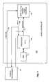
- Microcontrollers such as 100 depicted in FIG. 1generally include a processor (Central Processing Unit) 106 and associated Random Access Memory (RAM) 110 as well as a block of nonvolatile memory 116 , generally flash memory, used to store a user program.
- a block of user programmable nonvolatile memory 116the microcontroller may be customized to carry out any desired function within the capabilities of the device.
- Numerous techniques exist for programming the user program into the nonvolatile memory 116In general, such techniques may be characterized by use of an external tester/programmer 120 coupled directly to the nonvolatile memory 116 .
- the tester/programmer 120utilizes a control signal line 124 to appropriately signal the nonvolatile memory 116 (as well as associated circuitry within the microcontroller 100 ) that a programming mode is being entered. An address line, path or bus 130 is then used to identify memory locations within the nonvolatile memory 116 being programmed. Data is transmitted to the nonvolatile memory 116 over a data line, path or bus 138 . When all address locations have been appropriately programmed within the nonvolatile memory 116 , the tester/programmer 120 issues appropriate control signals on control path 124 to terminate the programming process. Thus, the tester/programmer 120 can directly manipulate the memory 116 with nothing to prevent unauthorized tampering with or copying the memory content.
- the present inventionrelates generally to controlling access to memory blocks. Objects, advantages and features of the invention will become apparent to those skilled in the art upon consideration of the following detailed description of the invention.
- a microcontrollerprovides protection to memory blocks in an embedded memory.
- a set of rulessuch as security levels mapped to memory blocks are stored in a nonvolatile memory.
- An algorithm for application of the rulesis stored, for example, in a supervisory ROM.
- the rulesare applied according to the algorithm in order to authorize or reject the read or write operation.
- Security levelscan be modified, according to defined rules. In one embodiment, the security levels can only be increased. This provides many advantages including the advantages that the memory security cannot be decreased below a default value established by the user. and intruders may be thwarted from attempts to modify the memory content in secure memory blocks.
- a method of accessing a block of memoryincludes, in response to an access request to the block of memory, ascertaining a security rule associated with the block of memory; applying the security rule according to a security algorithm to determine if the access request is authorized; and denying the access request in the event the access request is unauthorized.
- a method of accessing memoryincludes mapping a security level to each block of a plurality of memory blocks and storing the mapping in a table; in response to an access request to a specified block of memory, determining the security level for the specified block of memory; applying the a security algorithm using the security level to determine if the access request is authorized by the algorithm; and denying the access request in the event the access request is unauthorized.
- a method of controlling secure access to memoryinclude, in response to a request to change a security rule for a block of memory, determining if the change in the security rule for the block of memory is authorized; and denying the request in the event the request is unauthorized.
- FIG. 1is a block diagram illustrating a conventional microcontroller with external access to memory.
- FIG. 2is a block diagram of a microcontroller consistent with an embodiment of the present invention.
- FIG. 3is a flow chart describing a process of accessing protected memory blocks consistent with an embodiment of the invention.
- FIG. 4is a flow chart describing another process of accessing protected memory blocks consistent with an embodiment of the invention.
- FIG. 5is a flow chart describing a process of modifying security levels for memory blocks consistent with an embodiment of the present invention.
- FIG. 6is a flow chart describing another process of modifying security levels for memory blocks consistent with an embodiment of the present invention.
- these quantitiestake the form of electrical or magnetic signals capable of being stored, transferred, combined, compared, and otherwise manipulated in a computer system. It has proven convenient at times, principally for reasons of common usage, to refer to these signals as bits, values, elements, symbols, characters, terms, numbers, or the like.
- processor 206is coupled to internal Random Access Memory (RAM) 210 .
- Nonvolatile memory 216e.g., Flash memory
- supervisor nonvolatile memory 218is also connected to processor 206 .
- a control path 224is provided from processor 206 to nonvolatile memory 216 and 218 .
- conventional address path 230 and data path 238 from processor 206 to memory 216 and 218is provided.
- microcontroller 200includes a control program ROM (a supervisor ROM) 244 that contains hard-coded instructions used by processor 206 to directly program memory locations of nonvolatile memory 216 .
- control program ROMa supervisor ROM
- all programming of nonvolatile memory 216is carried out by an internally stored process executing as a program on processor 206 .
- a tester/programmer 220may be coupled to microcontroller 200 via a path 250 which, in the preferred embodiment, is a two wire bus carrying control, address and data information to an internal test/control interface 260 .
- the test/control interface 260is coupled to processor 206 to provide the processor with program instructions and other test and control function instructions from the tester/programmer 220 . Instructions from the tester/programmer 220 are stored in an instruction queue 268 for sequential retrieval and execution by processor 206 .
- the user programis stored in nonvolatile memory 216 which is arranged in memory blocks.
- this memory 216provides 16 Megabytes of storage for user program and is divided into 256 memory blocks.
- this particular arrangementis to be considered exemplary since any other arrangement could also be used with the present invention.
- the supervisory nonvolatile memory 218contains a table mapping a security level for each of the memory blocks in the user program nonvolatile memory 216 .
- four security levels 0 through 3are defined as illustrated in TABLE 1 below.
- security level 0is the least secure and security level 3 is the most secure. It is, however, somewhat ambiguous whether security level 2 is more or less secure than security level 1, since the actual security of these middle levels is somewhat application dependent.
- the security levelsmay be defined by setting two bits in a memory table. The number of bits can be adjusted if more or fewer security levels are to be used.
- the supervisor nonvolatile memory 218stores a table similar to TABLE 2 below to define the security level of each of the 256 blocks of memory 216 .
- the security levels presentedare presented for illustrative purposes and do not represent a default security level or have any other particular significance.
- block 0is shown to have the highest security level, while block 4 has the lowest security level.
- Blocks 1 and 255have security level 2 and blocks 2 and 3 have security level 1.
- these security levelsare programmed at the time of manufacture in accord with the end user's requirements. The security levels can subsequently be changed under certain circumstances either by programming using tester/programmer 220 or through actions of processor 206 operating under program control. However, as a security measure, the security levels can only be changed in a prescribed manner.
- the security levels assigned to the memory blockscan only be changed under control of an algorithm stored in the supervisor ROM 244 in accordance with rules stored in the supervisor nonvolatile memory 218 .
- rules in memory 218in accordance with one embodiment define the security levels and permissible transitions in security levels as will be described later.
- passwords, unique identifications for users, encryption and other security measurescould equally well be applied using the general principles of the present invention.
- the security levelcan only be increased, not decreased.
- changing from one intermediate level to the otheris not permitted.
- the permissible transitions in security levelsis described in TABLE 3 below for the current example.
- these permissible transitionscan be hard coded within the algorithm in supervisor ROM 244 or may form a type of rule defined by the supervisor nonvolatile memory 218 that is referenced in carrying out the security measures of the present invention.
- the security level of memory block 4is initially assigned as 0.
- the security levelcould be increased to level 2 by action of tester/programmer 220 and then subsequently increased to security level 3 by action of the tester/programmer.
- the only way to modify the security level to reduce itis to erase the supervisor nonvolatile memory 218 and re-initialize the microcontroller. This action will result in the user defined default security levels being restored.
- the security level of memory block 4would obviously return to 0 since there is no way to reach this insecure level except by it being so defined as a user default.
- a process 300 of providing security to memory blocks within nonvolatile memory 216 in accordance with an embodiment of the present inventionstarts at 304 .
- an instructionis received at 310
- the memory blockis looked up in the protection table of supervisory nonvolatile memory 218 .
- the processor 206determines through the supervisor programs stored in supervisor ROM 244 whether or not the read or write operation is authorized at 338 based upon the security algorithm residing in ROM 244 and the rules defined in memory 218 . If the read or write operation is authorized at 338 , then the operation is executed at 344 and control returns to 310 . However, in the event the operation is not authorized at 338 , the operation is rejected and an error condition exists at 352 . Any number of actions can take place as a result of such an error condition at 352 including shutdown of the microcontroller 200 , presenting an error message, presenting an alert or any other suitable action. In certain embodiments, control may then be passed from 352 back to 310 to await the next instruction.
- Process 300 of FIG. 3can be generalized as process 400 of FIG. 4 .
- an instructionis received at 310 , it is determined at 316 whether the instruction is a read or write operation to a protected memory block within nonvolatile user memory 216 . If not, normal processing of the instruction is carried out at 320 and control returns to 310 to await the next instruction. However, if the instruction is a read or write instruction to protected memory 216 at 316 control passes to 324 where the memory block for the read or write operation is identified.
- security rules for the identified memory blockare read from the supervisory nonvolatile memory 218 . These rules are applied to determine if the read or write operation is permitted using the security algorithm stored in supervisory ROM 244 at 420 .
- the read or write operationis permitted at 430 , then the read or write operation is executed at 344 and control returns to 310 to await the next instruction. However, if the read or write operation is not permitted at 430 , the operation is rejected and an error condition exists at 352 .
- the security level for any given memory block within the nonvolatile user memory 216can be modified by action of processor 206 under program control or under control of tester/programmer 220 .
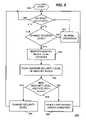
- One embodiment of a process used to determine whether or not a transition in security level is permittedis illustrated as process 500 of FIG. 5 which starts at 504 .
- processor 206determines if the instruction is for a change in security level at 518 . If not, normal operation proceeds at 522 and control returns to 512 to await the next instruction (either from tester programmer 220 or by operation of another program on processor 206 ).
- the memory block to be changedis identified at 526 and the current security level of the memory block is read at 532 from the supervisor nonvolatile memory 218 .
- transitions in security levelare only permitted if a transition increases security. Therefore, at 538 the current security level and the proposed new security level are examined to determine if the new security level is higher than the old level. If so, the security level is modified at 544 and control returns to 522 . If, however, the new security level is not higher than the old security level at 538 , the change is rejected and an error condition is flagged at 550 .
- error conditionscan result in any number of operational steps including disabling the microcontroller 200 .
- processor 206determines if the instruction is for a change in security level at 518 . If not, normal operation proceeds at 522 and control returns to 512 to await the next instruction (either from tester programmer 220 or by operation of another program on processor 206 ). If, at 518 , the instruction directs a security level change, the memory block to be changed is identified at 526 and the current security level of the memory block is read at 532 from the supervisor nonvolatile memory 218 .
- the transitionis permitted under the rules and algorithm defined for permissible transitions of security level. If the transition in security level is permitted at 616 , then the security level is modified at 544 and control returns to 522 . If, however, the transition is not permitted at 616 , the change is rejected and an error condition is flagged at 550 . Depending on the nature of the operational program of the microcontroller 200 , such error conditions can result in any number of operational steps including disabling the microcontroller 200 .
- the present inventionis used to protect memory locations in a nonvolatile user program memory 216 .
- the rulesare stored in the nonvolatile supervisory memory 218 and the algorithm for applying the rules is stored in the supervisor ROM 244 .
- this arrangementshould not be considered limiting since this invention can be configured in other ways without departing from the invention.
- both the rules and the algorithmcould be stored in ROM.
- the protected memorycould be random access memory or read only memory or nonvolatile Flash memory or a combination thereof. Such embodiments are considered equivalents for purposes of this invention.
- the present inventionis preferably implemented using a programmed processor executing programming instructions that are broadly described above in flow chart form. Such instructions can be stored in any suitable electronic programming medium.
- Such instructionscan be stored in any suitable electronic programming medium.
- those skilled in the artwill appreciate that the processes described above can be implemented in any number of variations and in many suitable programming languages without departing from the present invention. For example, the order of certain operations carried out can often be varied, and additional operations can be added without departing from the invention. Error trapping can be added and/or enhanced and variations can be made in user interface and information presentation without departing from the present invention. Such variations are contemplated and considered equivalent.
- the present inventionprovides enhanced security by virtue of isolating not only the control lines, data lines and address lines of the nonvolatile memory from the tester/programmer but also isolates the tester/programmer from the actual process used to effect the programming or re-programming of the nonvolatile memory 216 .
- the security procedures described aboveare used so that only modifications to the content of the nonvolatile memory that are within prescribed security limits can be carried out.
- the invention as describedprovides substantially enhanced security against intruders attempting to program or re-program the nonvolatile memory 216 .
- the present inventionis preferably implemented using a programmed processor executing programming instructions that are broadly described above in flow chart form. Such instructions may be stored in any suitable electronic programming medium.
- Such instructionsmay be stored in any suitable electronic programming medium.
- those skilled in the artwill appreciate that the processes described above may be implemented in any number of variations and in many suitable programming languages without departing from the present invention. For example, the order of certain operations carried out can often be varied, and additional operations may be added without departing from the invention. Error trapping may be added and/or enhanced and variations may be made in user interface and information presentation without departing from the present invention. Such variations are contemplated and considered equivalent.
Landscapes
- Engineering & Computer Science (AREA)
- Theoretical Computer Science (AREA)
- Computer Security & Cryptography (AREA)
- Computer Hardware Design (AREA)
- Physics & Mathematics (AREA)
- General Engineering & Computer Science (AREA)
- General Physics & Mathematics (AREA)
- Software Systems (AREA)
- Storage Device Security (AREA)
- Microcomputers (AREA)
Abstract
Description
| TABLE 1 | |
| Security | |
| Level | Definition |
| 0 | unsecure - no read protect, no write protect |
| 1 | read protect, write protect, processor can self modify |
| 2 | read protect, no processor self modify, no write protect |
| 3 | full read protect, full write protect |
| TABLE 2 | |||
| Block | Security | ||
| Number | Level | ||
| 0 | 3 | ||
| 1 | 2 | ||
| 2 | 1 | ||
| 3 | 1 | ||
| 4 | 0 | ||
| . . . | . . . | ||
| 255 | 2 | ||
| TABLE 3 | |||
| Security | Transition | ||
| Transition | Allowed? | ||
| 0 to 1 | YES | ||
| 0 to 2 | YES | ||
| 0 to 3 | YES? | ||
| 1 to 0 | NO? | ||
| 1 to 2 | NO | ||
| 1 to 3 | YES | ||
| 2 to 0 | NO? | ||
| 2 to 1 | NO | ||
| 2 to 3 | NO? | ||
| 3 to 0 | NO? | ||
| 3 to 1 | NO? | ||
| 3 to 2 | NO? | ||
Claims (15)
Priority Applications (1)
| Application Number | Priority Date | Filing Date | Title |
|---|---|---|---|
| US09/855,868US6952778B1 (en) | 2000-10-26 | 2001-05-14 | Protecting access to microcontroller memory blocks |
Applications Claiming Priority (2)
| Application Number | Priority Date | Filing Date | Title |
|---|---|---|---|
| US24370800P | 2000-10-26 | 2000-10-26 | |
| US09/855,868US6952778B1 (en) | 2000-10-26 | 2001-05-14 | Protecting access to microcontroller memory blocks |
Publications (1)
| Publication Number | Publication Date |
|---|---|
| US6952778B1true US6952778B1 (en) | 2005-10-04 |
Family
ID=35005229
Family Applications (1)
| Application Number | Title | Priority Date | Filing Date |
|---|---|---|---|
| US09/855,868Expired - LifetimeUS6952778B1 (en) | 2000-10-26 | 2001-05-14 | Protecting access to microcontroller memory blocks |
Country Status (1)
| Country | Link |
|---|---|
| US (1) | US6952778B1 (en) |
Cited By (59)
| Publication number | Priority date | Publication date | Assignee | Title |
|---|---|---|---|---|
| US20020133715A1 (en)* | 2000-12-04 | 2002-09-19 | Giovanni Benini | Method for using a data processing system as a function of an authorization, associated data processing system and associated program |
| US20030115472A1 (en)* | 2001-12-19 | 2003-06-19 | Chang L-Lang | Data protection method and device by using address |
| US20050033978A1 (en)* | 2003-08-08 | 2005-02-10 | Hyser Chris D. | Method and system for securing a computer system |
| US20050108488A1 (en)* | 2001-09-21 | 2005-05-19 | Peter Rohm | Programme-controlled unit |
| US20060037007A1 (en)* | 2004-08-13 | 2006-02-16 | Warren Snyder | Providing hardware independence to automate code generation of processing device firmware |
| US20060191002A1 (en)* | 2005-02-21 | 2006-08-24 | Samsung Electronics Co., Ltd. | Packet security method and apparatus |
| US20070271212A1 (en)* | 2006-05-17 | 2007-11-22 | Galois Connections Inc. | Document accessing through multiple security domains including multi-tear wiki webpage and/or using cross domain trusted service |
| US20070273659A1 (en)* | 2006-05-26 | 2007-11-29 | Xiaoping Jiang | Multi-function slider in touchpad |
| US20070282752A1 (en)* | 2006-05-17 | 2007-12-06 | Galois Connections Inc. | Document accessing through multiple security domains |
| US20080109747A1 (en)* | 2006-11-08 | 2008-05-08 | Cao Andrew H | Dynamic input field protection |
| US20080263334A1 (en)* | 2007-04-17 | 2008-10-23 | Cypress Semiconductor Corp. | Dynamically configurable and re-configurable data path |
| US20090327577A1 (en)* | 2008-06-27 | 2009-12-31 | Microsoft Corporation | Hybrid storage |
| US20100106954A1 (en)* | 2008-10-23 | 2010-04-29 | Robert Michael Muchsel | Multi-Layer Content Protecting Microcontroller |
| US7737724B2 (en) | 2007-04-17 | 2010-06-15 | Cypress Semiconductor Corporation | Universal digital block interconnection and channel routing |
| US7761845B1 (en) | 2002-09-09 | 2010-07-20 | Cypress Semiconductor Corporation | Method for parameterizing a user module |
| US7765095B1 (en) | 2000-10-26 | 2010-07-27 | Cypress Semiconductor Corporation | Conditional branching in an in-circuit emulation system |
| US7770113B1 (en) | 2001-11-19 | 2010-08-03 | Cypress Semiconductor Corporation | System and method for dynamically generating a configuration datasheet |
| US7774190B1 (en) | 2001-11-19 | 2010-08-10 | Cypress Semiconductor Corporation | Sleep and stall in an in-circuit emulation system |
| US7825688B1 (en) | 2000-10-26 | 2010-11-02 | Cypress Semiconductor Corporation | Programmable microcontroller architecture(mixed analog/digital) |
| US20100281145A1 (en)* | 2009-05-04 | 2010-11-04 | Cypress Semiconductor Corporation | Autonomous control in a programmable system |
| US7844437B1 (en) | 2001-11-19 | 2010-11-30 | Cypress Semiconductor Corporation | System and method for performing next placements and pruning of disallowed placements for programming an integrated circuit |
| JP2010286866A (en)* | 2009-06-09 | 2010-12-24 | Oki Semiconductor Co Ltd | Microcontroller device |
| US20110010773A1 (en)* | 2009-07-07 | 2011-01-13 | Kuity Corp. | Hardware command filter matrix integrated circuit with restriced command enforcement capability |
| US7893724B2 (en) | 2004-03-25 | 2011-02-22 | Cypress Semiconductor Corporation | Method and circuit for rapid alignment of signals |
| US8026739B2 (en) | 2007-04-17 | 2011-09-27 | Cypress Semiconductor Corporation | System level interconnect with programmable switching |
| US8042093B1 (en) | 2001-11-15 | 2011-10-18 | Cypress Semiconductor Corporation | System providing automatic source code generation for personalization and parameterization of user modules |
| US8040266B2 (en) | 2007-04-17 | 2011-10-18 | Cypress Semiconductor Corporation | Programmable sigma-delta analog-to-digital converter |
| US8049569B1 (en) | 2007-09-05 | 2011-11-01 | Cypress Semiconductor Corporation | Circuit and method for improving the accuracy of a crystal-less oscillator having dual-frequency modes |
| US8067948B2 (en) | 2006-03-27 | 2011-11-29 | Cypress Semiconductor Corporation | Input/output multiplexer bus |
| US8069428B1 (en) | 2001-10-24 | 2011-11-29 | Cypress Semiconductor Corporation | Techniques for generating microcontroller configuration information |
| US8069405B1 (en) | 2001-11-19 | 2011-11-29 | Cypress Semiconductor Corporation | User interface for efficiently browsing an electronic document using data-driven tabs |
| US8078970B1 (en) | 2001-11-09 | 2011-12-13 | Cypress Semiconductor Corporation | Graphical user interface with user-selectable list-box |
| US8078894B1 (en) | 2007-04-25 | 2011-12-13 | Cypress Semiconductor Corporation | Power management architecture, method and configuration system |
| US8082531B2 (en) | 2004-08-13 | 2011-12-20 | Cypress Semiconductor Corporation | Method and an apparatus to design a processing system using a graphical user interface |
| US8085100B2 (en) | 2005-02-04 | 2011-12-27 | Cypress Semiconductor Corporation | Poly-phase frequency synthesis oscillator |
| US8085067B1 (en) | 2005-12-21 | 2011-12-27 | Cypress Semiconductor Corporation | Differential-to-single ended signal converter circuit and method |
| US8089461B2 (en) | 2005-06-23 | 2012-01-03 | Cypress Semiconductor Corporation | Touch wake for electronic devices |
| US8092083B2 (en) | 2007-04-17 | 2012-01-10 | Cypress Semiconductor Corporation | Temperature sensor with digital bandgap |
| US8103497B1 (en) | 2002-03-28 | 2012-01-24 | Cypress Semiconductor Corporation | External interface for event architecture |
| US8103496B1 (en) | 2000-10-26 | 2012-01-24 | Cypress Semicondutor Corporation | Breakpoint control in an in-circuit emulation system |
| US8120408B1 (en) | 2005-05-05 | 2012-02-21 | Cypress Semiconductor Corporation | Voltage controlled oscillator delay cell and method |
| US8130025B2 (en) | 2007-04-17 | 2012-03-06 | Cypress Semiconductor Corporation | Numerical band gap |
| US8149048B1 (en) | 2000-10-26 | 2012-04-03 | Cypress Semiconductor Corporation | Apparatus and method for programmable power management in a programmable analog circuit block |
| US8160864B1 (en) | 2000-10-26 | 2012-04-17 | Cypress Semiconductor Corporation | In-circuit emulator and pod synchronized boot |
| US8176296B2 (en) | 2000-10-26 | 2012-05-08 | Cypress Semiconductor Corporation | Programmable microcontroller architecture |
| US20120191933A1 (en)* | 2010-09-21 | 2012-07-26 | Texas Instruments Incorporated | Device Security Features Supporting a Distributed Shared Memory System |
| US8286125B2 (en) | 2004-08-13 | 2012-10-09 | Cypress Semiconductor Corporation | Model for a hardware device-independent method of defining embedded firmware for programmable systems |
| US8402313B1 (en) | 2002-05-01 | 2013-03-19 | Cypress Semiconductor Corporation | Reconfigurable testing system and method |
| US8499270B1 (en) | 2007-04-25 | 2013-07-30 | Cypress Semiconductor Corporation | Configuration of programmable IC design elements |
| US8516025B2 (en) | 2007-04-17 | 2013-08-20 | Cypress Semiconductor Corporation | Clock driven dynamic datapath chaining |
| US8527949B1 (en) | 2001-11-19 | 2013-09-03 | Cypress Semiconductor Corporation | Graphical user interface for dynamically reconfiguring a programmable device |
| US8537121B2 (en) | 2006-05-26 | 2013-09-17 | Cypress Semiconductor Corporation | Multi-function slider in touchpad |
| CN104412242A (en)* | 2012-06-27 | 2015-03-11 | 北欧半导体公司 | Memory protection |
| US20160259004A1 (en)* | 2015-03-05 | 2016-09-08 | Advanced Digital Chips Inc. | Debugger and debugging system |
| US9514300B2 (en)* | 2011-02-22 | 2016-12-06 | Redwall Technologies, Llc | Systems and methods for enhanced security in wireless communication |
| US9720805B1 (en) | 2007-04-25 | 2017-08-01 | Cypress Semiconductor Corporation | System and method for controlling a target device |
| US9990505B2 (en) | 2014-08-12 | 2018-06-05 | Redwall Technologies, Llc | Temporally isolating data accessed by a computing device |
| US20180326735A1 (en)* | 2015-11-09 | 2018-11-15 | Hangzhou Chipjet Technology Co.,Ltd. | Printer Chip, Ink Cartridge and Printer Chip Storage Allocation Method |
| EP4557106A1 (en)* | 2023-11-17 | 2025-05-21 | STMicroelectronics International N.V. | Method for operating a non-volatile memory |
Citations (5)
| Publication number | Priority date | Publication date | Assignee | Title |
|---|---|---|---|---|
| US5202687A (en) | 1991-06-12 | 1993-04-13 | Intellectual Property Development Associates Of Connecticut | Analog to digital converter |
| US5737760A (en)* | 1995-10-06 | 1998-04-07 | Motorola Inc. | Microcontroller with security logic circuit which prevents reading of internal memory by external program |
| US6003133A (en)* | 1997-11-17 | 1999-12-14 | Motorola, Inc. | Data processor with a privileged state firewall and method therefore |
| US6144327A (en) | 1996-08-15 | 2000-11-07 | Intellectual Property Development Associates Of Connecticut, Inc. | Programmably interconnected programmable devices |
| US6339815B1 (en)* | 1998-08-14 | 2002-01-15 | Silicon Storage Technology, Inc. | Microcontroller system having allocation circuitry to selectively allocate and/or hide portions of a program memory address space |
- 2001
- 2001-05-14USUS09/855,868patent/US6952778B1/ennot_activeExpired - Lifetime
Patent Citations (5)
| Publication number | Priority date | Publication date | Assignee | Title |
|---|---|---|---|---|
| US5202687A (en) | 1991-06-12 | 1993-04-13 | Intellectual Property Development Associates Of Connecticut | Analog to digital converter |
| US5737760A (en)* | 1995-10-06 | 1998-04-07 | Motorola Inc. | Microcontroller with security logic circuit which prevents reading of internal memory by external program |
| US6144327A (en) | 1996-08-15 | 2000-11-07 | Intellectual Property Development Associates Of Connecticut, Inc. | Programmably interconnected programmable devices |
| US6003133A (en)* | 1997-11-17 | 1999-12-14 | Motorola, Inc. | Data processor with a privileged state firewall and method therefore |
| US6339815B1 (en)* | 1998-08-14 | 2002-01-15 | Silicon Storage Technology, Inc. | Microcontroller system having allocation circuitry to selectively allocate and/or hide portions of a program memory address space |
Non-Patent Citations (1)
| Title |
|---|
| Atmel Corporation: AT90SC Summay: "Secure Microcontrollers for Smart Cards", Oct. 1999, pp. 1-7.* |
Cited By (96)
| Publication number | Priority date | Publication date | Assignee | Title |
|---|---|---|---|---|
| US8555032B2 (en) | 2000-10-26 | 2013-10-08 | Cypress Semiconductor Corporation | Microcontroller programmable system on a chip with programmable interconnect |
| US8736303B2 (en) | 2000-10-26 | 2014-05-27 | Cypress Semiconductor Corporation | PSOC architecture |
| US9843327B1 (en) | 2000-10-26 | 2017-12-12 | Cypress Semiconductor Corporation | PSOC architecture |
| US10725954B2 (en) | 2000-10-26 | 2020-07-28 | Monterey Research, Llc | Microcontroller programmable system on a chip |
| US10020810B2 (en) | 2000-10-26 | 2018-07-10 | Cypress Semiconductor Corporation | PSoC architecture |
| US10248604B2 (en) | 2000-10-26 | 2019-04-02 | Cypress Semiconductor Corporation | Microcontroller programmable system on a chip |
| US10261932B2 (en) | 2000-10-26 | 2019-04-16 | Cypress Semiconductor Corporation | Microcontroller programmable system on a chip |
| US7825688B1 (en) | 2000-10-26 | 2010-11-02 | Cypress Semiconductor Corporation | Programmable microcontroller architecture(mixed analog/digital) |
| US8358150B1 (en) | 2000-10-26 | 2013-01-22 | Cypress Semiconductor Corporation | Programmable microcontroller architecture(mixed analog/digital) |
| US7765095B1 (en) | 2000-10-26 | 2010-07-27 | Cypress Semiconductor Corporation | Conditional branching in an in-circuit emulation system |
| US9766650B2 (en) | 2000-10-26 | 2017-09-19 | Cypress Semiconductor Corporation | Microcontroller programmable system on a chip with programmable interconnect |
| US8103496B1 (en) | 2000-10-26 | 2012-01-24 | Cypress Semicondutor Corporation | Breakpoint control in an in-circuit emulation system |
| US8149048B1 (en) | 2000-10-26 | 2012-04-03 | Cypress Semiconductor Corporation | Apparatus and method for programmable power management in a programmable analog circuit block |
| US8176296B2 (en) | 2000-10-26 | 2012-05-08 | Cypress Semiconductor Corporation | Programmable microcontroller architecture |
| US8160864B1 (en) | 2000-10-26 | 2012-04-17 | Cypress Semiconductor Corporation | In-circuit emulator and pod synchronized boot |
| US20020133715A1 (en)* | 2000-12-04 | 2002-09-19 | Giovanni Benini | Method for using a data processing system as a function of an authorization, associated data processing system and associated program |
| US20050108488A1 (en)* | 2001-09-21 | 2005-05-19 | Peter Rohm | Programme-controlled unit |
| US8793635B1 (en) | 2001-10-24 | 2014-07-29 | Cypress Semiconductor Corporation | Techniques for generating microcontroller configuration information |
| US10466980B2 (en) | 2001-10-24 | 2019-11-05 | Cypress Semiconductor Corporation | Techniques for generating microcontroller configuration information |
| US8069428B1 (en) | 2001-10-24 | 2011-11-29 | Cypress Semiconductor Corporation | Techniques for generating microcontroller configuration information |
| US8078970B1 (en) | 2001-11-09 | 2011-12-13 | Cypress Semiconductor Corporation | Graphical user interface with user-selectable list-box |
| US10698662B2 (en) | 2001-11-15 | 2020-06-30 | Cypress Semiconductor Corporation | System providing automatic source code generation for personalization and parameterization of user modules |
| US8042093B1 (en) | 2001-11-15 | 2011-10-18 | Cypress Semiconductor Corporation | System providing automatic source code generation for personalization and parameterization of user modules |
| US8533677B1 (en) | 2001-11-19 | 2013-09-10 | Cypress Semiconductor Corporation | Graphical user interface for dynamically reconfiguring a programmable device |
| US8370791B2 (en) | 2001-11-19 | 2013-02-05 | Cypress Semiconductor Corporation | System and method for performing next placements and pruning of disallowed placements for programming an integrated circuit |
| US7844437B1 (en) | 2001-11-19 | 2010-11-30 | Cypress Semiconductor Corporation | System and method for performing next placements and pruning of disallowed placements for programming an integrated circuit |
| US8527949B1 (en) | 2001-11-19 | 2013-09-03 | Cypress Semiconductor Corporation | Graphical user interface for dynamically reconfiguring a programmable device |
| US7770113B1 (en) | 2001-11-19 | 2010-08-03 | Cypress Semiconductor Corporation | System and method for dynamically generating a configuration datasheet |
| US8069405B1 (en) | 2001-11-19 | 2011-11-29 | Cypress Semiconductor Corporation | User interface for efficiently browsing an electronic document using data-driven tabs |
| US7774190B1 (en) | 2001-11-19 | 2010-08-10 | Cypress Semiconductor Corporation | Sleep and stall in an in-circuit emulation system |
| US20030115472A1 (en)* | 2001-12-19 | 2003-06-19 | Chang L-Lang | Data protection method and device by using address |
| US8103497B1 (en) | 2002-03-28 | 2012-01-24 | Cypress Semiconductor Corporation | External interface for event architecture |
| US8402313B1 (en) | 2002-05-01 | 2013-03-19 | Cypress Semiconductor Corporation | Reconfigurable testing system and method |
| US7761845B1 (en) | 2002-09-09 | 2010-07-20 | Cypress Semiconductor Corporation | Method for parameterizing a user module |
| US7398390B2 (en)* | 2003-08-08 | 2008-07-08 | Hewlett-Packard Development Company, L.P. | Method and system for securing a computer system |
| US20050033978A1 (en)* | 2003-08-08 | 2005-02-10 | Hyser Chris D. | Method and system for securing a computer system |
| US7893724B2 (en) | 2004-03-25 | 2011-02-22 | Cypress Semiconductor Corporation | Method and circuit for rapid alignment of signals |
| US8082531B2 (en) | 2004-08-13 | 2011-12-20 | Cypress Semiconductor Corporation | Method and an apparatus to design a processing system using a graphical user interface |
| US8539398B2 (en) | 2004-08-13 | 2013-09-17 | Cypress Semiconductor Corporation | Model for a hardware device-independent method of defining embedded firmware for programmable systems |
| US8069436B2 (en) | 2004-08-13 | 2011-11-29 | Cypress Semiconductor Corporation | Providing hardware independence to automate code generation of processing device firmware |
| US20060037007A1 (en)* | 2004-08-13 | 2006-02-16 | Warren Snyder | Providing hardware independence to automate code generation of processing device firmware |
| US8286125B2 (en) | 2004-08-13 | 2012-10-09 | Cypress Semiconductor Corporation | Model for a hardware device-independent method of defining embedded firmware for programmable systems |
| US8085100B2 (en) | 2005-02-04 | 2011-12-27 | Cypress Semiconductor Corporation | Poly-phase frequency synthesis oscillator |
| US20060191002A1 (en)* | 2005-02-21 | 2006-08-24 | Samsung Electronics Co., Ltd. | Packet security method and apparatus |
| US8438629B2 (en)* | 2005-02-21 | 2013-05-07 | Samsung Electronics Co., Ltd. | Packet security method and apparatus |
| US8120408B1 (en) | 2005-05-05 | 2012-02-21 | Cypress Semiconductor Corporation | Voltage controlled oscillator delay cell and method |
| US8089461B2 (en) | 2005-06-23 | 2012-01-03 | Cypress Semiconductor Corporation | Touch wake for electronic devices |
| US8085067B1 (en) | 2005-12-21 | 2011-12-27 | Cypress Semiconductor Corporation | Differential-to-single ended signal converter circuit and method |
| US8717042B1 (en) | 2006-03-27 | 2014-05-06 | Cypress Semiconductor Corporation | Input/output multiplexer bus |
| US8067948B2 (en) | 2006-03-27 | 2011-11-29 | Cypress Semiconductor Corporation | Input/output multiplexer bus |
| US8166559B2 (en)* | 2006-05-17 | 2012-04-24 | Galois, Inc. | Document accessing through multiple security domains including multi-tear wiki webpage and/or using cross domain trusted service |
| US8171557B2 (en) | 2006-05-17 | 2012-05-01 | Galois, Inc. | Document accessing through multiple security domains |
| US20070282752A1 (en)* | 2006-05-17 | 2007-12-06 | Galois Connections Inc. | Document accessing through multiple security domains |
| US20070271212A1 (en)* | 2006-05-17 | 2007-11-22 | Galois Connections Inc. | Document accessing through multiple security domains including multi-tear wiki webpage and/or using cross domain trusted service |
| US20070273659A1 (en)* | 2006-05-26 | 2007-11-29 | Xiaoping Jiang | Multi-function slider in touchpad |
| US8089472B2 (en) | 2006-05-26 | 2012-01-03 | Cypress Semiconductor Corporation | Bidirectional slider with delete function |
| US8537121B2 (en) | 2006-05-26 | 2013-09-17 | Cypress Semiconductor Corporation | Multi-function slider in touchpad |
| US7716596B2 (en) | 2006-11-08 | 2010-05-11 | International Business Machines Corporation | Dynamic input field protection |
| US20080109747A1 (en)* | 2006-11-08 | 2008-05-08 | Cao Andrew H | Dynamic input field protection |
| US20080263334A1 (en)* | 2007-04-17 | 2008-10-23 | Cypress Semiconductor Corp. | Dynamically configurable and re-configurable data path |
| US9564902B2 (en) | 2007-04-17 | 2017-02-07 | Cypress Semiconductor Corporation | Dynamically configurable and re-configurable data path |
| US8092083B2 (en) | 2007-04-17 | 2012-01-10 | Cypress Semiconductor Corporation | Temperature sensor with digital bandgap |
| US8130025B2 (en) | 2007-04-17 | 2012-03-06 | Cypress Semiconductor Corporation | Numerical band gap |
| US8476928B1 (en) | 2007-04-17 | 2013-07-02 | Cypress Semiconductor Corporation | System level interconnect with programmable switching |
| US7737724B2 (en) | 2007-04-17 | 2010-06-15 | Cypress Semiconductor Corporation | Universal digital block interconnection and channel routing |
| US8516025B2 (en) | 2007-04-17 | 2013-08-20 | Cypress Semiconductor Corporation | Clock driven dynamic datapath chaining |
| US8040266B2 (en) | 2007-04-17 | 2011-10-18 | Cypress Semiconductor Corporation | Programmable sigma-delta analog-to-digital converter |
| US8026739B2 (en) | 2007-04-17 | 2011-09-27 | Cypress Semiconductor Corporation | System level interconnect with programmable switching |
| US8499270B1 (en) | 2007-04-25 | 2013-07-30 | Cypress Semiconductor Corporation | Configuration of programmable IC design elements |
| US9720805B1 (en) | 2007-04-25 | 2017-08-01 | Cypress Semiconductor Corporation | System and method for controlling a target device |
| US8909960B1 (en) | 2007-04-25 | 2014-12-09 | Cypress Semiconductor Corporation | Power management architecture, method and configuration system |
| US8078894B1 (en) | 2007-04-25 | 2011-12-13 | Cypress Semiconductor Corporation | Power management architecture, method and configuration system |
| US8049569B1 (en) | 2007-09-05 | 2011-11-01 | Cypress Semiconductor Corporation | Circuit and method for improving the accuracy of a crystal-less oscillator having dual-frequency modes |
| US20090327577A1 (en)* | 2008-06-27 | 2009-12-31 | Microsoft Corporation | Hybrid storage |
| US8555015B2 (en)* | 2008-10-23 | 2013-10-08 | Maxim Integrated Products, Inc. | Multi-layer content protecting microcontroller |
| US9311255B2 (en)* | 2008-10-23 | 2016-04-12 | Maxim Integrated Products, Inc. | Multi-layer content protecting microcontroller |
| CN102197382B (en)* | 2008-10-23 | 2016-01-13 | 马克西姆综合产品公司 | Multilayer Content Protection Microcontroller |
| US20100106954A1 (en)* | 2008-10-23 | 2010-04-29 | Robert Michael Muchsel | Multi-Layer Content Protecting Microcontroller |
| US20140040584A1 (en)* | 2008-10-23 | 2014-02-06 | Maxim Integrated Products, Inc. | Multi-layer content protecting microcontroller |
| US20100281145A1 (en)* | 2009-05-04 | 2010-11-04 | Cypress Semiconductor Corporation | Autonomous control in a programmable system |
| US9448964B2 (en) | 2009-05-04 | 2016-09-20 | Cypress Semiconductor Corporation | Autonomous control in a programmable system |
| JP2010286866A (en)* | 2009-06-09 | 2010-12-24 | Oki Semiconductor Co Ltd | Microcontroller device |
| US20110010773A1 (en)* | 2009-07-07 | 2011-01-13 | Kuity Corp. | Hardware command filter matrix integrated circuit with restriced command enforcement capability |
| US8683114B2 (en)* | 2010-09-21 | 2014-03-25 | Texas Instruments Incorporated | Device security features supporting a distributed shared memory system |
| US20120191933A1 (en)* | 2010-09-21 | 2012-07-26 | Texas Instruments Incorporated | Device Security Features Supporting a Distributed Shared Memory System |
| US9514300B2 (en)* | 2011-02-22 | 2016-12-06 | Redwall Technologies, Llc | Systems and methods for enhanced security in wireless communication |
| KR20150033695A (en)* | 2012-06-27 | 2015-04-01 | 노르딕 세미컨덕터 에이에스에이 | Memory protection |
| TWI581099B (en)* | 2012-06-27 | 2017-05-01 | 北歐半導體公司 | Integrated-circuit and method of controlling memory access on the integrated-circuit device |
| CN104412242A (en)* | 2012-06-27 | 2015-03-11 | 北欧半导体公司 | Memory protection |
| US9430409B2 (en) | 2012-06-27 | 2016-08-30 | Nordic Semiconductor Asa | Memory protection |
| EP3702923A1 (en) | 2012-06-27 | 2020-09-02 | Nordic Semiconductor ASA | Memory protection |
| US9990505B2 (en) | 2014-08-12 | 2018-06-05 | Redwall Technologies, Llc | Temporally isolating data accessed by a computing device |
| US20160259004A1 (en)* | 2015-03-05 | 2016-09-08 | Advanced Digital Chips Inc. | Debugger and debugging system |
| US20180326735A1 (en)* | 2015-11-09 | 2018-11-15 | Hangzhou Chipjet Technology Co.,Ltd. | Printer Chip, Ink Cartridge and Printer Chip Storage Allocation Method |
| EP4557106A1 (en)* | 2023-11-17 | 2025-05-21 | STMicroelectronics International N.V. | Method for operating a non-volatile memory |
| FR3155620A1 (en)* | 2023-11-17 | 2025-05-23 | Stmicroelectronics International N.V. | Method of operating a non-volatile memory |
Similar Documents
| Publication | Publication Date | Title |
|---|---|---|
| US6952778B1 (en) | Protecting access to microcontroller memory blocks | |
| US10360411B2 (en) | Secure processing unit systems and methods | |
| CN101238473B (en) | A secure terminal and a method of protecting a secret key | |
| US8566927B2 (en) | Method for detecting and reacting against possible attack to security enforcing operation performed by a cryptographic token or card | |
| KR100929870B1 (en) | How to keep BIOS security of computer system | |
| JP3396043B2 (en) | Micro circuit | |
| US6160734A (en) | Method for ensuring security of program data in one-time programmable memory | |
| KR100319677B1 (en) | Memory access control unit | |
| US20080022396A1 (en) | Memory data protection device and IC card LSI | |
| US12147588B2 (en) | Controlled access to data stored in a secure partition | |
| JPS6046744B2 (en) | Computer operating system security devices | |
| JP2008257734A (en) | Security control in data processing system based on memory domain | |
| US20080263256A1 (en) | Logic Device with Write Protected Memory Management Unit Registers | |
| KR20190085387A (en) | Semiconductor device and method for operating semiconductor device | |
| US6079019A (en) | IC memory card | |
| US6240493B1 (en) | Method and apparatus for performing access censorship in a data processing system | |
| US5901311A (en) | Access key protection for computer system data | |
| US20060184799A1 (en) | Security circuit and method to secure information in a device | |
| US10296738B2 (en) | Secure integrated-circuit state management | |
| EP3454216A1 (en) | Method for protecting unauthorized data access from a memory | |
| CN109376530B (en) | Process mandatory behavior control method and system based on mark | |
| CA1085517A (en) | Hardware control storage area protection method and means | |
| US6779099B2 (en) | Operation method for controlling access attributes of a memorized page of a memory unit and its structure | |
| US20040186947A1 (en) | Access control system for nonvolatile memory | |
| WO2001097010A2 (en) | Data processing method and device for protected execution of instructions |
Legal Events
| Date | Code | Title | Description |
|---|---|---|---|
| STCF | Information on status: patent grant | Free format text:PATENTED CASE | |
| REMI | Maintenance fee reminder mailed | ||
| FPAY | Fee payment | Year of fee payment:4 | |
| SULP | Surcharge for late payment | ||
| FPAY | Fee payment | Year of fee payment:8 | |
| AS | Assignment | Owner name:MORGAN STANLEY SENIOR FUNDING, INC., NEW YORK Free format text:SECURITY INTEREST;ASSIGNORS:CYPRESS SEMICONDUCTOR CORPORATION;SPANSION LLC;REEL/FRAME:035240/0429 Effective date:20150312 | |
| FPAY | Fee payment | Year of fee payment:12 | |
| AS | Assignment | Owner name:CYPRESS SEMICONDUCTOR CORPORATION, CALIFORNIA Free format text:ASSIGNMENT OF ASSIGNORS INTEREST;ASSIGNOR:SNYDER, WARREN;REEL/FRAME:043296/0159 Effective date:20170720 | |
| AS | Assignment | Owner name:MUFG UNION BANK, N.A., CALIFORNIA Free format text:ASSIGNMENT AND ASSUMPTION OF SECURITY INTEREST IN INTELLECTUAL PROPERTY;ASSIGNOR:MORGAN STANLEY SENIOR FUNDING, INC.;REEL/FRAME:050896/0366 Effective date:20190731 | |
| AS | Assignment | Owner name:LONGITUDE FLASH MEMORY SOLUTIONS LIMITED, IRELAND Free format text:ASSIGNMENT OF ASSIGNORS INTEREST;ASSIGNOR:CYPRESS SEMICONDUCTOR CORPORATION;REEL/FRAME:051251/0787 Effective date:20191206 | |
| AS | Assignment | Owner name:CYPRESS SEMICONDUCTOR CORPORATION, CALIFORNIA Free format text:RELEASE BY SECURED PARTY;ASSIGNOR:MUFG UNION BANK, N.A.;REEL/FRAME:051334/0633 Effective date:20191206 | |
| AS | Assignment | Owner name:MORGAN STANLEY SENIOR FUNDING, INC., NEW YORK Free format text:CORRECTIVE ASSIGNMENT TO CORRECT THE 8647899 PREVIOUSLY RECORDED ON REEL 035240 FRAME 0429. ASSIGNOR(S) HEREBY CONFIRMS THE SECURITY INTERST;ASSIGNORS:CYPRESS SEMICONDUCTOR CORPORATION;SPANSION LLC;REEL/FRAME:058002/0470 Effective date:20150312 |