US6952047B2 - Assemblies having stacked semiconductor chips and methods of making same - Google Patents
Assemblies having stacked semiconductor chips and methods of making sameDownload PDFInfo
- Publication number
- US6952047B2 US6952047B2US10/611,390US61139003AUS6952047B2US 6952047 B2US6952047 B2US 6952047B2US 61139003 AUS61139003 AUS 61139003AUS 6952047 B2US6952047 B2US 6952047B2
- Authority
- US
- United States
- Prior art keywords
- microelectronic element
- substrate
- contacts
- terminals
- pads
- Prior art date
- Legal status (The legal status is an assumption and is not a legal conclusion. Google has not performed a legal analysis and makes no representation as to the accuracy of the status listed.)
- Expired - Lifetime
Links
Images


Classifications
- H—ELECTRICITY
- H01—ELECTRIC ELEMENTS
- H01L—SEMICONDUCTOR DEVICES NOT COVERED BY CLASS H10
- H01L25/00—Assemblies consisting of a plurality of semiconductor or other solid state devices
- H01L25/03—Assemblies consisting of a plurality of semiconductor or other solid state devices all the devices being of a type provided for in a single subclass of subclasses H10B, H10D, H10F, H10H, H10K or H10N, e.g. assemblies of rectifier diodes
- H01L25/04—Assemblies consisting of a plurality of semiconductor or other solid state devices all the devices being of a type provided for in a single subclass of subclasses H10B, H10D, H10F, H10H, H10K or H10N, e.g. assemblies of rectifier diodes the devices not having separate containers
- H01L25/065—Assemblies consisting of a plurality of semiconductor or other solid state devices all the devices being of a type provided for in a single subclass of subclasses H10B, H10D, H10F, H10H, H10K or H10N, e.g. assemblies of rectifier diodes the devices not having separate containers the devices being of a type provided for in group H10D89/00
- H01L25/0657—Stacked arrangements of devices
- H—ELECTRICITY
- H01—ELECTRIC ELEMENTS
- H01L—SEMICONDUCTOR DEVICES NOT COVERED BY CLASS H10
- H01L2224/00—Indexing scheme for arrangements for connecting or disconnecting semiconductor or solid-state bodies and methods related thereto as covered by H01L24/00
- H01L2224/01—Means for bonding being attached to, or being formed on, the surface to be connected, e.g. chip-to-package, die-attach, "first-level" interconnects; Manufacturing methods related thereto
- H01L2224/02—Bonding areas; Manufacturing methods related thereto
- H01L2224/04—Structure, shape, material or disposition of the bonding areas prior to the connecting process
- H01L2224/05—Structure, shape, material or disposition of the bonding areas prior to the connecting process of an individual bonding area
- H01L2224/0554—External layer
- H01L2224/0556—Disposition
- H01L2224/05568—Disposition the whole external layer protruding from the surface
- H—ELECTRICITY
- H01—ELECTRIC ELEMENTS
- H01L—SEMICONDUCTOR DEVICES NOT COVERED BY CLASS H10
- H01L2224/00—Indexing scheme for arrangements for connecting or disconnecting semiconductor or solid-state bodies and methods related thereto as covered by H01L24/00
- H01L2224/01—Means for bonding being attached to, or being formed on, the surface to be connected, e.g. chip-to-package, die-attach, "first-level" interconnects; Manufacturing methods related thereto
- H01L2224/02—Bonding areas; Manufacturing methods related thereto
- H01L2224/04—Structure, shape, material or disposition of the bonding areas prior to the connecting process
- H01L2224/05—Structure, shape, material or disposition of the bonding areas prior to the connecting process of an individual bonding area
- H01L2224/0554—External layer
- H01L2224/05573—Single external layer
- H—ELECTRICITY
- H01—ELECTRIC ELEMENTS
- H01L—SEMICONDUCTOR DEVICES NOT COVERED BY CLASS H10
- H01L2224/00—Indexing scheme for arrangements for connecting or disconnecting semiconductor or solid-state bodies and methods related thereto as covered by H01L24/00
- H01L2224/01—Means for bonding being attached to, or being formed on, the surface to be connected, e.g. chip-to-package, die-attach, "first-level" interconnects; Manufacturing methods related thereto
- H01L2224/10—Bump connectors; Manufacturing methods related thereto
- H01L2224/15—Structure, shape, material or disposition of the bump connectors after the connecting process
- H01L2224/16—Structure, shape, material or disposition of the bump connectors after the connecting process of an individual bump connector
- H01L2224/161—Disposition
- H01L2224/16151—Disposition the bump connector connecting between a semiconductor or solid-state body and an item not being a semiconductor or solid-state body, e.g. chip-to-substrate, chip-to-passive
- H01L2224/16221—Disposition the bump connector connecting between a semiconductor or solid-state body and an item not being a semiconductor or solid-state body, e.g. chip-to-substrate, chip-to-passive the body and the item being stacked
- H01L2224/16225—Disposition the bump connector connecting between a semiconductor or solid-state body and an item not being a semiconductor or solid-state body, e.g. chip-to-substrate, chip-to-passive the body and the item being stacked the item being non-metallic, e.g. insulating substrate with or without metallisation
- H—ELECTRICITY
- H01—ELECTRIC ELEMENTS
- H01L—SEMICONDUCTOR DEVICES NOT COVERED BY CLASS H10
- H01L2224/00—Indexing scheme for arrangements for connecting or disconnecting semiconductor or solid-state bodies and methods related thereto as covered by H01L24/00
- H01L2224/01—Means for bonding being attached to, or being formed on, the surface to be connected, e.g. chip-to-package, die-attach, "first-level" interconnects; Manufacturing methods related thereto
- H01L2224/26—Layer connectors, e.g. plate connectors, solder or adhesive layers; Manufacturing methods related thereto
- H01L2224/31—Structure, shape, material or disposition of the layer connectors after the connecting process
- H01L2224/32—Structure, shape, material or disposition of the layer connectors after the connecting process of an individual layer connector
- H01L2224/321—Disposition
- H01L2224/32135—Disposition the layer connector connecting between different semiconductor or solid-state bodies, i.e. chip-to-chip
- H01L2224/32145—Disposition the layer connector connecting between different semiconductor or solid-state bodies, i.e. chip-to-chip the bodies being stacked
- H—ELECTRICITY
- H01—ELECTRIC ELEMENTS
- H01L—SEMICONDUCTOR DEVICES NOT COVERED BY CLASS H10
- H01L2224/00—Indexing scheme for arrangements for connecting or disconnecting semiconductor or solid-state bodies and methods related thereto as covered by H01L24/00
- H01L2224/01—Means for bonding being attached to, or being formed on, the surface to be connected, e.g. chip-to-package, die-attach, "first-level" interconnects; Manufacturing methods related thereto
- H01L2224/42—Wire connectors; Manufacturing methods related thereto
- H01L2224/47—Structure, shape, material or disposition of the wire connectors after the connecting process
- H01L2224/48—Structure, shape, material or disposition of the wire connectors after the connecting process of an individual wire connector
- H01L2224/4805—Shape
- H01L2224/4809—Loop shape
- H01L2224/48091—Arched
- H—ELECTRICITY
- H01—ELECTRIC ELEMENTS
- H01L—SEMICONDUCTOR DEVICES NOT COVERED BY CLASS H10
- H01L2224/00—Indexing scheme for arrangements for connecting or disconnecting semiconductor or solid-state bodies and methods related thereto as covered by H01L24/00
- H01L2224/01—Means for bonding being attached to, or being formed on, the surface to be connected, e.g. chip-to-package, die-attach, "first-level" interconnects; Manufacturing methods related thereto
- H01L2224/42—Wire connectors; Manufacturing methods related thereto
- H01L2224/47—Structure, shape, material or disposition of the wire connectors after the connecting process
- H01L2224/48—Structure, shape, material or disposition of the wire connectors after the connecting process of an individual wire connector
- H01L2224/481—Disposition
- H01L2224/48151—Connecting between a semiconductor or solid-state body and an item not being a semiconductor or solid-state body, e.g. chip-to-substrate, chip-to-passive
- H01L2224/48221—Connecting between a semiconductor or solid-state body and an item not being a semiconductor or solid-state body, e.g. chip-to-substrate, chip-to-passive the body and the item being stacked
- H01L2224/48225—Connecting between a semiconductor or solid-state body and an item not being a semiconductor or solid-state body, e.g. chip-to-substrate, chip-to-passive the body and the item being stacked the item being non-metallic, e.g. insulating substrate with or without metallisation
- H01L2224/48227—Connecting between a semiconductor or solid-state body and an item not being a semiconductor or solid-state body, e.g. chip-to-substrate, chip-to-passive the body and the item being stacked the item being non-metallic, e.g. insulating substrate with or without metallisation connecting the wire to a bond pad of the item
- H—ELECTRICITY
- H01—ELECTRIC ELEMENTS
- H01L—SEMICONDUCTOR DEVICES NOT COVERED BY CLASS H10
- H01L2224/00—Indexing scheme for arrangements for connecting or disconnecting semiconductor or solid-state bodies and methods related thereto as covered by H01L24/00
- H01L2224/01—Means for bonding being attached to, or being formed on, the surface to be connected, e.g. chip-to-package, die-attach, "first-level" interconnects; Manufacturing methods related thereto
- H01L2224/42—Wire connectors; Manufacturing methods related thereto
- H01L2224/47—Structure, shape, material or disposition of the wire connectors after the connecting process
- H01L2224/48—Structure, shape, material or disposition of the wire connectors after the connecting process of an individual wire connector
- H01L2224/484—Connecting portions
- H—ELECTRICITY
- H01—ELECTRIC ELEMENTS
- H01L—SEMICONDUCTOR DEVICES NOT COVERED BY CLASS H10
- H01L2224/00—Indexing scheme for arrangements for connecting or disconnecting semiconductor or solid-state bodies and methods related thereto as covered by H01L24/00
- H01L2224/73—Means for bonding being of different types provided for in two or more of groups H01L2224/10, H01L2224/18, H01L2224/26, H01L2224/34, H01L2224/42, H01L2224/50, H01L2224/63, H01L2224/71
- H01L2224/732—Location after the connecting process
- H01L2224/73201—Location after the connecting process on the same surface
- H01L2224/73203—Bump and layer connectors
- H01L2224/73204—Bump and layer connectors the bump connector being embedded into the layer connector
- H—ELECTRICITY
- H01—ELECTRIC ELEMENTS
- H01L—SEMICONDUCTOR DEVICES NOT COVERED BY CLASS H10
- H01L2224/00—Indexing scheme for arrangements for connecting or disconnecting semiconductor or solid-state bodies and methods related thereto as covered by H01L24/00
- H01L2224/73—Means for bonding being of different types provided for in two or more of groups H01L2224/10, H01L2224/18, H01L2224/26, H01L2224/34, H01L2224/42, H01L2224/50, H01L2224/63, H01L2224/71
- H01L2224/732—Location after the connecting process
- H01L2224/73201—Location after the connecting process on the same surface
- H01L2224/73215—Layer and wire connectors
- H—ELECTRICITY
- H01—ELECTRIC ELEMENTS
- H01L—SEMICONDUCTOR DEVICES NOT COVERED BY CLASS H10
- H01L2224/00—Indexing scheme for arrangements for connecting or disconnecting semiconductor or solid-state bodies and methods related thereto as covered by H01L24/00
- H01L2224/73—Means for bonding being of different types provided for in two or more of groups H01L2224/10, H01L2224/18, H01L2224/26, H01L2224/34, H01L2224/42, H01L2224/50, H01L2224/63, H01L2224/71
- H01L2224/732—Location after the connecting process
- H01L2224/73251—Location after the connecting process on different surfaces
- H01L2224/73265—Layer and wire connectors
- H—ELECTRICITY
- H01—ELECTRIC ELEMENTS
- H01L—SEMICONDUCTOR DEVICES NOT COVERED BY CLASS H10
- H01L2225/00—Details relating to assemblies covered by the group H01L25/00 but not provided for in its subgroups
- H01L2225/03—All the devices being of a type provided for in the same main group of the same subclass of class H10, e.g. assemblies of rectifier diodes
- H01L2225/04—All the devices being of a type provided for in the same main group of the same subclass of class H10, e.g. assemblies of rectifier diodes the devices not having separate containers
- H01L2225/065—All the devices being of a type provided for in the same main group of the same subclass of class H10
- H01L2225/06503—Stacked arrangements of devices
- H01L2225/0651—Wire or wire-like electrical connections from device to substrate
- H—ELECTRICITY
- H01—ELECTRIC ELEMENTS
- H01L—SEMICONDUCTOR DEVICES NOT COVERED BY CLASS H10
- H01L2225/00—Details relating to assemblies covered by the group H01L25/00 but not provided for in its subgroups
- H01L2225/03—All the devices being of a type provided for in the same main group of the same subclass of class H10, e.g. assemblies of rectifier diodes
- H01L2225/04—All the devices being of a type provided for in the same main group of the same subclass of class H10, e.g. assemblies of rectifier diodes the devices not having separate containers
- H01L2225/065—All the devices being of a type provided for in the same main group of the same subclass of class H10
- H01L2225/06503—Stacked arrangements of devices
- H01L2225/06517—Bump or bump-like direct electrical connections from device to substrate
- H—ELECTRICITY
- H01—ELECTRIC ELEMENTS
- H01L—SEMICONDUCTOR DEVICES NOT COVERED BY CLASS H10
- H01L2225/00—Details relating to assemblies covered by the group H01L25/00 but not provided for in its subgroups
- H01L2225/03—All the devices being of a type provided for in the same main group of the same subclass of class H10, e.g. assemblies of rectifier diodes
- H01L2225/04—All the devices being of a type provided for in the same main group of the same subclass of class H10, e.g. assemblies of rectifier diodes the devices not having separate containers
- H01L2225/065—All the devices being of a type provided for in the same main group of the same subclass of class H10
- H01L2225/06503—Stacked arrangements of devices
- H01L2225/06541—Conductive via connections through the device, e.g. vertical interconnects, through silicon via [TSV]
- H—ELECTRICITY
- H01—ELECTRIC ELEMENTS
- H01L—SEMICONDUCTOR DEVICES NOT COVERED BY CLASS H10
- H01L2225/00—Details relating to assemblies covered by the group H01L25/00 but not provided for in its subgroups
- H01L2225/03—All the devices being of a type provided for in the same main group of the same subclass of class H10, e.g. assemblies of rectifier diodes
- H01L2225/04—All the devices being of a type provided for in the same main group of the same subclass of class H10, e.g. assemblies of rectifier diodes the devices not having separate containers
- H01L2225/065—All the devices being of a type provided for in the same main group of the same subclass of class H10
- H01L2225/06503—Stacked arrangements of devices
- H01L2225/06582—Housing for the assembly, e.g. chip scale package [CSP]
- H01L2225/06586—Housing with external bump or bump-like connectors
- H—ELECTRICITY
- H01—ELECTRIC ELEMENTS
- H01L—SEMICONDUCTOR DEVICES NOT COVERED BY CLASS H10
- H01L24/00—Arrangements for connecting or disconnecting semiconductor or solid-state bodies; Methods or apparatus related thereto
- H01L24/73—Means for bonding being of different types provided for in two or more of groups H01L24/10, H01L24/18, H01L24/26, H01L24/34, H01L24/42, H01L24/50, H01L24/63, H01L24/71
- H—ELECTRICITY
- H01—ELECTRIC ELEMENTS
- H01L—SEMICONDUCTOR DEVICES NOT COVERED BY CLASS H10
- H01L2924/00—Indexing scheme for arrangements or methods for connecting or disconnecting semiconductor or solid-state bodies as covered by H01L24/00
- H01L2924/01—Chemical elements
- H01L2924/01079—Gold [Au]
- H—ELECTRICITY
- H01—ELECTRIC ELEMENTS
- H01L—SEMICONDUCTOR DEVICES NOT COVERED BY CLASS H10
- H01L2924/00—Indexing scheme for arrangements or methods for connecting or disconnecting semiconductor or solid-state bodies as covered by H01L24/00
- H01L2924/15—Details of package parts other than the semiconductor or other solid state devices to be connected
- H01L2924/151—Die mounting substrate
- H01L2924/153—Connection portion
- H01L2924/1531—Connection portion the connection portion being formed only on the surface of the substrate opposite to the die mounting surface
- H01L2924/15311—Connection portion the connection portion being formed only on the surface of the substrate opposite to the die mounting surface being a ball array, e.g. BGA
- H—ELECTRICITY
- H01—ELECTRIC ELEMENTS
- H01L—SEMICONDUCTOR DEVICES NOT COVERED BY CLASS H10
- H01L2924/00—Indexing scheme for arrangements or methods for connecting or disconnecting semiconductor or solid-state bodies as covered by H01L24/00
- H01L2924/30—Technical effects
- H01L2924/301—Electrical effects
- H01L2924/3025—Electromagnetic shielding
Definitions
- the present inventionrelates to stacked microelectronic assemblies, to methods of forming such assemblies, and to components useful in such assemblies.
- a standard chiphas a flat, rectangular body with a relatively expansive front face having contacts connected to the internal circuitry of the chip.
- Each individual chipis mounted in a package, which in turn is connected to a circuit panel, such as a printed circuit board, so that the contacts of the chip are connected to conductors of the circuit panel.
- a circuit panelsuch as a printed circuit board
- the front face of the chipfaces the circuit panel, and the contacts on the chip are connected to the circuit panel by solder balls or other connecting elements.
- the chip packageoccupies an area of the circuit panel considerably larger than the area of the chip itself.
- the total area of a plurality of chips mounted on a circuit panelis also a concern.
- Various proposalshave been advanced for providing plural chips in a single package or module. It has been proposed to package plural chips in a “stacked” arrangement, i.e., an arrangement where chips are placed one on top of another. In a stacked arrangement, several chips can be mounted in an area of the circuit panel that is less than the total area of the chips.
- Certain stacked chip arrangementsare disclosed, for example, in certain embodiments of the aforementioned '977 and '265 patents and in U.S. Pat. No. 5,347,159, the disclosures of which are hereby incorporated by reference herein.
- the present inventionaddresses these needs.
- a microelectronic assemblycomprises a first microelectronic element having a first face with first contacts exposed at the first face. The first face faces in a first direction.
- a second microelectronic elementhas a first side with second contacts exposed at the first side. The first side faces in a second direction opposite to the first direction.
- the assemblyincludes a substrate underlying the first microelectronic element and the second microelectronic element. The substrate has first terminals, second terminals, and at least one third terminal. The first contacts are connected to the first terminals and the second contacts are connected to the second terminals.
- a conductive memberis disposed between the first microelectronic element and the second microelectronic element.
- the conductive memberis connected to the at least one third terminal.
- An assembly according to this aspectdesirably comprises a stacked arrangement of two microelectronic elements facing in opposite directions and having a conductive member disposed therebetween.
- the microelectronic elementsare connected to a substrate having terminals for forming connections with external elements, such as circuit boards or other microelectronic elements.
- the conductive membermay comprise a ground plane or an electromagnetic interference shield.
- the first face of the first microelectronic elementfaces the substrate and the first side of the second microelectronic element faces away from the substrate.
- the second microelectronic elementdesirably overlies the first microelectronic element.
- the substratemay have a first surface facing the first microelectronic element and the second microelectronic element.
- the substratemay also have a second surface facing in a direction opposite from the first surface.
- the features of the substratedesirably include pads exposed at the first surface of the substrate.
- the substrateincludes first pads connected to the first terminals.
- the first contactsmay be connected to the first pads.
- the first terminalsare connected to the first pads and are desirably exposed at the second surface of the substrate.
- the first padsare connected to the first contacts by masses of bonding material.
- a dielectric materialis desirably disposed between the first face of the first microelectronic element and the first surface of the substrate, and in-between the masses of bonding material.
- a dielectric materialmay also be disposed over the substrate, first microelectronic element and second microelectronic element.
- the substratemay include second pads exposed at the first surface of the substrate and connected to the second terminals.
- the second contacts of the second microelectronic elementmay be connected to the second pads.
- the second contacts and second padsare connected by wires.
- the second terminalsare desirably exposed at the second surface of the substrate.
- the terminalsdesirably include vias extending through the substrate.
- the substratemay include at least one third pad connected to the at least one third terminal.
- the conductive elementmay be connected to the at least one third pad.
- the third terminalis desirably exposed at the second surface of the substrate.
- the conductive elementmay be connected to the at least one third pad by at least one wire.
- the second pads and at least one third padare disposed outwardly from the first microelectronic element.
- the first microelectronic elementhas a second face facing oppositely from the first face and the second microelectronic element has a second side facing oppositely from the first side.
- the conductive elementis desirably disposed between the second face and the second side. The conductive element may be adhered to the second face and second side.
- the substratemay comprise an edge.
- the first padsare exposed at the first surface of the substrate.
- the first contactsmay be connected to the first pads by a conductive element, such as a wire, extending transversely to the edge.
- the substratemay comprise an aperture and the first contacts may be connected to the first pads by a wire or other conductive element, extending through the aperture.
- the conductive memberhas a first width and the second microelectronic element has a second width less than the first width.
- the second microelectronic elementoverlies a first portion of the conductive member and a second portion of the conductive member lies outwardly of the second microelectronic element.
- the substratemay include at least one pad exposed at the first surface of the substrate, the at least one pad being connected to the at least one third terminal, and the conductive member may be connected to the at least one pad at the second portion of the conductive member, outwardly of the second microelectronic element.
- a method of making a microelectronic assemblycomprises providing a substrate having a plurality of pads, including first pads, second pads and at least one third pad. The pads are exposed at a first surface of the substrate. A first microelectronic element is arranged with the substrate. The method includes connecting first contacts exposed on a first face of the first microelectronic element to the first pads on the substrate.
- a second microelectronic element and a conductive memberare arranged with the substrate and first microelectronic element so that the conductive member is disposed between the first microelectronic element and the second microelectronic element.
- a first side of the second microelectronic elementhas second contacts exposed thereat.
- the second contactsare connected to the second pads and the conductive member is connected to the at least one third pad.
- Methods according to this aspect of the present inventionprovide a method of making a stacked microelectronic assembly having a conductive member disposed in the space between a first microelectronic element and a second microelectronic element.
- Methods according to embodiments of the present inventionprovide a method for forming electromagnetic shielding or a ground plane between microelectronic elements in a stacked electronic assembly.
- the assemblymay comprise further microelectronic elements.
- the conductive membermay comprise a plate of electrically conductive material.
- the conductive membermay comprise an aluminum plate.
- the conductive memberis connected to the first microelectronic element and the second microelectronic element is connected to the conductive member. In certain preferred embodiments, the conductive member is connected to the at least one third pad before the second contacts are connected to the second pads.
- the first face of the first microelectronic elementmay face the first surface of the substrate and the first contacts may be connected before the second contacts and the conductive member.
- the step of connecting the first contacts to the first padsincludes disposing masses of bonding material between first contacts and the first pads.
- the step of connecting the first contacts to the first padsmay include attaching wires to the first contacts and the first pads.
- the first microelectronic elementhas a second face facing in a direction opposite to the first face.
- the step of connecting the conductive membermay include applying adhesive to the second face and attaching the conductive member to the second face.
- An adhesivemay be applied to the conductive member and a second side of the second microelectronic element is attached to the conductive member.
- the second side of the microelectronic elementfaces in a direction opposite to the first side.
- the adhesivemay be cured after the step of connecting the second microelectronic element to the conductive member.
- Methods according to certain embodiments of the present inventioninclude a conductive member for shielding or ground connection that is disposed between two microelectronic elements facing in opposite directions.
- the step of connecting the second contacts to the second padsmay include attaching wires to the second contacts and the second pads.
- the conductive membermay be connected to the at least one third pad by attaching wires to the conductive member and the third pad.
- the third padmay be arranged for connection with a ground or voltage source.
- a flowable materialis desirably introduced so as to surround at least the second contacts, second pads and third pads.
- a flowable materialis desirably introduced between the first face of the first microelectronic element and the first surface of the substrate so as to surround the first pads and first contacts, after the step of connecting the first contacts to the first pads.
- the conductive membermay be wider than the second microelectronic element and a portion of the conductive member disposed outwardly of the second microelectronic element may be connected to the at least one third pad.
- FIG. 1is a cross-sectional view of the substrate with a plurality of vias
- FIG. 2is a cross-sectional view of the substrate with a first microelectronic element overlying the substrate;
- FIG. 3is a cross-sectional view depicting the substrate and first microelectronic element at a later stage in the method
- FIG. 4is a cross-sectional view wherein an adhesive is overlying the first microelectronic element
- FIG. 5is a cross-sectional view of a conductive element being placed on top of the first microelectronic element
- FIG. 6is a cross-sectional view depicting the assembly of FIG. 5 at a later stage in the method
- FIG. 7is a cross-sectional view of packages formed in the method of FIGS. 1-6 with a second microelectronic element included overlying the assembly;
- FIG. 8is a cross-sectional view of an individual assembly formed in a method in accordance with a further embodiment of the present invention.
- FIG. 9is a cross-sectional view of an individual assembly formed in a method in accordance with another embodiment of the invention.
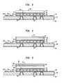
- FIGS. 1-7An embodiment of the invention is shown in FIGS. 1-7 .
- a substrate 10having a first surface 12 and a second surface 16 facing in a direction opposite from the first surface 12 .
- the substratedesirably comprises a rigid or flexible sheet of dielectric material.
- the substrate 10may comprise polyimide, other polymers, or other dielectric materials.
- the substratemay comprise FR4 or a circuit board material.
- the substrateincludes a plurality of vias 20 extending from the first surface 12 to the second surface 16 and pads 22 aligned with the vias 20 .
- the pads 22include first pads 22 a , second pads 22 b and third pads 22 c , as will be discussed further below.
- the pads in the embodiments shown in FIG. 1include first pads 22 a disposed at a central region of the substrate 10 and second pads 22 b and third pads 22 c disposed outwardly of the first pads.
- the padsmay have different arrangements with respect to one another.
- the first microelectronic element 24has a second face 28 that faces in the second direction 18 , in a direction opposite from the first face 26 .
- the contacts 27are connected to the first pads 22 a on the first surface 12 .
- the contacts 27are connected to first pads 22 a that are exposed at the second surface 16 of the substrate 10 .
- the first contacts 27are bonded to the first pads 22 a in a “flip-chip” arrangement with the substrate 10 , as shown in FIG. 2 .
- masses of bonding material 30are disposed between the first pads 22 a and the first contacts 27 .
- the masses of bonding material 30are brought to the reflow temperature of the bonding material and are then allowed to solidify so as to form a bond with the first contacts 27 and the first pads 22 a .
- the vias 20desirably have conductive material 32 disposed therein so as to line the vias 20 and form a connection with the pads 22 a .
- the conductive material 32is used in forming connections with external circuitry so that the substrate 10 interconnects the microelectronic elements with external circuitry.
- the conductive material 32may be deposited within the vias 20 before or after the first contacts 27 are connected to the first pads 22 a , but preferably before. As is known in the art, the conductive material 32 may be deposited in the vias 20 utilizing methods such as sputtering or other methods known in the art.
- a first dielectric material 35is desirably formed between the first face 26 and the first surface 12 , as shown in FIG. 3 .
- the first dielectric material 35may be introduced between the first face 26 and first surface 12 by disposing a flowable material therebetween so that the flowable material penetrates between the masses of bonding material 30 .
- the flowable materialis then cured to form the first dielectric material 35 .
- the first dielectric material 35may be formed from a flowable, curable polymer.
- a first layer of adhesive 37is applied to the second face 28 of the first microelectronic element 24 , as shown in FIG. 4.
- a first surface 38 of a conductive member 40is attached to the second face 28 utilizing the adhesive 37 , as shown in FIG. 5.
- a second layer of adhesive 42is then applied to the second surface 41 of the conductive member 40 .
- the second layer of adhesive 42is then utilized to connect the second microelectronic element 45 to the conductive member 40 , as shown in FIG. 6 .
- the first layer of adhesive and the second layer of adhesivemay comprise a flowable material applied onto the second face 28 and the second surface 41 of the conductive member 40 .
- the first layer of adhesive 37 and second layer of adhesive 42desirably comprise a thermal adhesive and the conductive member 40 may comprise a conductive plate, such as an aluminum plate.
- the conductive member 40comprises any electrically conductive material.
- the second microelectronic element 45has a first side 48 with a plurality of second contacts 50 exposed at the first side 48 .
- the second microelectronic element 45has a second side 52 facing in an opposite direction from the first side 48 .
- the second microelectronic element 45is assembled with the conductive member 40 so that the second side 52 abuts against the second layer of adhesive 42 , attaching the second side 52 to the second surface 41 of the conductive member 40 .
- the first layer of adhesive 37 and the second layer of adhesive 42are cured by applying thermal or radiant energy to the adhesive layers.
- the second layer of adhesive 42 and second microelectronic element 45are desirably smaller in width than the conductive member 40 so that after the second microelectronic element 45 is disposed on the conductive member 40 , a first portion of the conductive member 40 is covered by the second microelectronic element 45 , while a second portion 54 of the conductive member 40 lies outwardly of the second microelectronic element 45 .
- This second portion 54is then connected to the third pads 22 c on the first surface 12 of the substrate 10 .
- wires 58are attached at one end to third pads 22 c and then connected at a second end to the second portion 54 of the conductive member 40 .
- the second portion 54 lying outwardly of the second microelectronic element 45is utilized to connect to the substrate 10 .
- an edge 56 of the conductive membermay be used to connect to the third pads 22 c.
- the second contacts 50are connected to the second pads 22 b .
- wires 64are connected at one end to the second pads 22 b and then connected at another end to the second contacts 50 .
- the wiresmay be formed by a process known in the art as wire bonding.
- other conductive featuresare utilized to connect the pads of the substrate 10 to the first contacts 27 , the conductive member 40 and the second contacts 50 .
- any of these connectionsmay be formed by masses of bonding material, such as solder, or by leads formed on the substrate 10 , the first microelectronic element 24 and/or second microelectronic element 45 , or provided separately.
- the substrate 10desirably has terminals 60 that are exposed at the second surface 16 of the substrate 10 .
- the terminalsmay include solder balls 62 , disposed in the vias 20 .
- the solder balls 62are desirably deposited so as to connect with the conductive material 32 in the vias 20 .
- the terminals 60 binclude first terminals 60 a that are connected to the first pads 22 a , second terminals 60 b that are connected to the second pads 22 b and third terminals 60 c that are connected to the third pads 22 c .
- the terminals 60 care desirably arranged for forming the desired connections for the second contacts 50 .
- the first terminals 60 aare desirably arranged for forming the desired connections for the first contacts 27 .
- the third terminals 60 care arranged to form connections for the conductive member 40 , such as connections to a ground or voltage source, or other connections for electromagnetic interference shielding.
- the substrate 10may comprise one or more layers and may incorporate other features, such as traces or conductive planes.
- the pads and terminals carried by the substratedesirably comprise conductive materials commonly used to form electrical connections and used in making microelectronic elements and microelectronic components, such as copper and gold.
- the first microelectronic element 124is assembled with the substrate 110 and at least one aperture 111 is utilized to connect the first contacts 127 to first pads 122 a arranged on a surface of the substrate that faces away from the first microelectronic element 124 .
- wires 158are attached at one end to the first contacts 127 and then attached at another end to the first pads 122 a exposed on the second surface 116 of the substrate 110 .
- a first face 126 of the first microelectronic element 124faces the substrate 110 and may be attached to the substrate 110 using an adhesive.
- a dielectric layeris formed between the first face 126 and second face 112 .
- Such a dielectric layermay be formed as disclosed in certain embodiments of U.S. Pat. Nos. 5,679,977; 5,659,952; 5,706,174; and 6,169,328, the disclosures of which are hereby incorporated by reference herein.
- a substrate 210 having one or more windows 211 and a plurality of leads 258is assembled with the first microelectronic element 224 .
- the first microelectronic element 224 shown in FIG. 9has a first face 226 with a plurality of first contacts 227 exposed at a first face 226 , in a central region of the first face.
- contacts on the first microelectronic element and/or second microelectronic elementare arranged in one or more rows in a central region, at the periphery or distributed across the face or side of the microelectronic element.
- the leads 258 and substrate 210may be formed as disclosed in certain embodiments of U.S. Pat. No. 5,679,977, the disclosure of which is hereby incorporated by reference herein.
- microelectronic elementsare incorporated within the assembly.
- a dielectric padmay be mounted on the first side 48 of the second microelectronic element 45 shown in FIG. 7 .
- Another conductive member 40may be adhered to the pad and a third microelectronic element may be adhered to the conductive member.
- a third microelectronic elementmay be adhered to the dielectric pad on the first side 48 .
- a stack of microelectronic elements according to embodiments of the present inventionmay comprise any number of microelectronic elements.
Landscapes
- Engineering & Computer Science (AREA)
- Power Engineering (AREA)
- Microelectronics & Electronic Packaging (AREA)
- Physics & Mathematics (AREA)
- Condensed Matter Physics & Semiconductors (AREA)
- General Physics & Mathematics (AREA)
- Computer Hardware Design (AREA)
- Wire Bonding (AREA)
- Semiconductor Integrated Circuits (AREA)
Abstract
Description
Claims (24)
Priority Applications (2)
| Application Number | Priority Date | Filing Date | Title |
|---|---|---|---|
| US10/611,390US6952047B2 (en) | 2002-07-01 | 2003-07-01 | Assemblies having stacked semiconductor chips and methods of making same |
| US11/165,877US7229850B2 (en) | 2002-07-01 | 2005-06-24 | Method of making assemblies having stacked semiconductor chips |
Applications Claiming Priority (2)
| Application Number | Priority Date | Filing Date | Title |
|---|---|---|---|
| US39302602P | 2002-07-01 | 2002-07-01 | |
| US10/611,390US6952047B2 (en) | 2002-07-01 | 2003-07-01 | Assemblies having stacked semiconductor chips and methods of making same |
Related Child Applications (1)
| Application Number | Title | Priority Date | Filing Date |
|---|---|---|---|
| US11/165,877DivisionUS7229850B2 (en) | 2002-07-01 | 2005-06-24 | Method of making assemblies having stacked semiconductor chips |
Publications (2)
| Publication Number | Publication Date |
|---|---|
| US20040108581A1 US20040108581A1 (en) | 2004-06-10 |
| US6952047B2true US6952047B2 (en) | 2005-10-04 |
Family
ID=32474241
Family Applications (2)
| Application Number | Title | Priority Date | Filing Date |
|---|---|---|---|
| US10/611,390Expired - LifetimeUS6952047B2 (en) | 2002-07-01 | 2003-07-01 | Assemblies having stacked semiconductor chips and methods of making same |
| US11/165,877Expired - LifetimeUS7229850B2 (en) | 2002-07-01 | 2005-06-24 | Method of making assemblies having stacked semiconductor chips |
Family Applications After (1)
| Application Number | Title | Priority Date | Filing Date |
|---|---|---|---|
| US11/165,877Expired - LifetimeUS7229850B2 (en) | 2002-07-01 | 2005-06-24 | Method of making assemblies having stacked semiconductor chips |
Country Status (1)
| Country | Link |
|---|---|
| US (2) | US6952047B2 (en) |
Cited By (15)
| Publication number | Priority date | Publication date | Assignee | Title |
|---|---|---|---|---|
| US20050067712A1 (en)* | 2003-09-29 | 2005-03-31 | Toshikazu Imaoka | Semiconductor apparatus and method of fabricating the same |
| US20060003494A1 (en)* | 2004-06-30 | 2006-01-05 | Delin Li | Stacked package electronic device |
| US20070235865A1 (en)* | 2006-04-05 | 2007-10-11 | Infineon Technologies Ag | Semiconductor module havingdiscrete components and method for producing the same |
| US20080158844A1 (en)* | 2006-12-29 | 2008-07-03 | Advanced Semiconductor Engineering, Inc. | Stacked type chip package structure |
| US20080185736A1 (en)* | 1999-02-08 | 2008-08-07 | Megica Corporation | Multiple selectable function integrated circuit module |
| US20090057900A1 (en)* | 2005-05-03 | 2009-03-05 | Megica Corporation | Stacked Chip Package With Redistribution Lines |
| US7829986B2 (en)* | 2006-04-01 | 2010-11-09 | Stats Chippac Ltd. | Integrated circuit package system with net spacer |
| US20110133324A1 (en)* | 2009-12-03 | 2011-06-09 | Powertech Technology Inc. | Multi-chip stacked package and its mother chip to save interposer |
| US8021976B2 (en) | 2002-10-15 | 2011-09-20 | Megica Corporation | Method of wire bonding over active area of a semiconductor circuit |
| US8148806B2 (en) | 2000-05-19 | 2012-04-03 | Megica Corporation | Multiple chips bonded to packaging structure with low noise and multiple selectable functions |
| US8168527B2 (en) | 2006-09-06 | 2012-05-01 | Megica Corporation | Semiconductor chip and method for fabricating the same |
| US8294279B2 (en) | 2005-01-25 | 2012-10-23 | Megica Corporation | Chip package with dam bar restricting flow of underfill |
| US20130065363A1 (en)* | 2011-09-09 | 2013-03-14 | Dawning Leading Technology Inc. | Method for manufacturing a chip packaging structure |
| CN103000542A (en)* | 2011-09-16 | 2013-03-27 | 南茂科技股份有限公司 | Solder cap bump in semiconductor package and method of manufacturing the same |
| US8426982B2 (en) | 2001-03-30 | 2013-04-23 | Megica Corporation | Structure and manufacturing method of chip scale package |
Families Citing this family (8)
| Publication number | Priority date | Publication date | Assignee | Title |
|---|---|---|---|---|
| US10388626B2 (en)* | 2000-03-10 | 2019-08-20 | STATS ChipPAC Pte. Ltd. | Semiconductor device and method of forming flipchip interconnect structure |
| TW200536089A (en)* | 2004-03-03 | 2005-11-01 | United Test & Assembly Ct Ltd | Multiple stacked die window csp package and method of manufacture |
| US7531217B2 (en)* | 2004-12-15 | 2009-05-12 | Iowa State University Research Foundation, Inc. | Methods for making high-temperature coatings having Pt metal modified γ-Ni +γ′-Ni3Al alloy compositions and a reactive element |
| US7750482B2 (en)* | 2006-02-09 | 2010-07-06 | Stats Chippac Ltd. | Integrated circuit package system including zero fillet resin |
| WO2008007258A2 (en)* | 2006-06-20 | 2008-01-17 | Nxp B.V. | Power amplifier assembly |
| US20080150132A1 (en)* | 2006-12-21 | 2008-06-26 | Tom Hu | Stack up pcb substrate for high density interconnect packages |
| TWI376774B (en)* | 2007-06-08 | 2012-11-11 | Cyntec Co Ltd | Three dimensional package structure |
| US10271421B2 (en)* | 2016-09-30 | 2019-04-23 | Avago Technologies International Sales Pte. Limited | Systems and methods for providing electromagnetic interference (EMI) shielding between inductors of a radio frequency (RF) module |
Citations (16)
| Publication number | Priority date | Publication date | Assignee | Title |
|---|---|---|---|---|
| US4941033A (en) | 1988-12-27 | 1990-07-10 | Mitsubishi Denki Kabushiki Kaisha | Semiconductor integrated circuit device |
| US4982265A (en) | 1987-06-24 | 1991-01-01 | Hitachi, Ltd. | Semiconductor integrated circuit device and method of manufacturing the same |
| US5046238A (en) | 1990-03-15 | 1991-09-10 | Rogers Corporation | Method of manufacturing a multilayer circuit board |
| US5148266A (en) | 1990-09-24 | 1992-09-15 | Ist Associates, Inc. | Semiconductor chip assemblies having interposer and flexible lead |
| US5148265A (en) | 1990-09-24 | 1992-09-15 | Ist Associates, Inc. | Semiconductor chip assemblies with fan-in leads |
| US5222014A (en) | 1992-03-02 | 1993-06-22 | Motorola, Inc. | Three-dimensional multi-chip pad array carrier |
| US5440171A (en) | 1992-03-09 | 1995-08-08 | Hitachi, Ltd. | Semiconductor device with reinforcement |
| US5455740A (en) | 1994-03-07 | 1995-10-03 | Staktek Corporation | Bus communication system for stacked high density integrated circuit packages |
| US5646446A (en) | 1995-12-22 | 1997-07-08 | Fairchild Space And Defense Corporation | Three-dimensional flexible assembly of integrated circuits |
| US5659952A (en) | 1994-09-20 | 1997-08-26 | Tessera, Inc. | Method of fabricating compliant interface for semiconductor chip |
| US5679977A (en) | 1990-09-24 | 1997-10-21 | Tessera, Inc. | Semiconductor chip assemblies, methods of making same and components for same |
| US5706174A (en) | 1994-07-07 | 1998-01-06 | Tessera, Inc. | Compliant microelectrionic mounting device |
| US6169328B1 (en) | 1994-09-20 | 2001-01-02 | Tessera, Inc | Semiconductor chip assembly |
| US6573609B2 (en)* | 1997-11-25 | 2003-06-03 | Tessera, Inc. | Microelectronic component with rigid interposer |
| US6673651B2 (en)* | 1999-07-01 | 2004-01-06 | Oki Electric Industry Co., Ltd. | Method of manufacturing semiconductor device including semiconductor elements mounted on base plate |
| US6709895B1 (en)* | 1996-10-31 | 2004-03-23 | Tessera, Inc. | Packaged microelectronic elements with enhanced thermal conduction |
Family Cites Families (1)
| Publication number | Priority date | Publication date | Assignee | Title |
|---|---|---|---|---|
| US5834339A (en)* | 1996-03-07 | 1998-11-10 | Tessera, Inc. | Methods for providing void-free layers for semiconductor assemblies |
- 2003
- 2003-07-01USUS10/611,390patent/US6952047B2/ennot_activeExpired - Lifetime
- 2005
- 2005-06-24USUS11/165,877patent/US7229850B2/ennot_activeExpired - Lifetime
Patent Citations (17)
| Publication number | Priority date | Publication date | Assignee | Title |
|---|---|---|---|---|
| US4982265A (en) | 1987-06-24 | 1991-01-01 | Hitachi, Ltd. | Semiconductor integrated circuit device and method of manufacturing the same |
| US4941033A (en) | 1988-12-27 | 1990-07-10 | Mitsubishi Denki Kabushiki Kaisha | Semiconductor integrated circuit device |
| US5046238A (en) | 1990-03-15 | 1991-09-10 | Rogers Corporation | Method of manufacturing a multilayer circuit board |
| US5679977A (en) | 1990-09-24 | 1997-10-21 | Tessera, Inc. | Semiconductor chip assemblies, methods of making same and components for same |
| US5148266A (en) | 1990-09-24 | 1992-09-15 | Ist Associates, Inc. | Semiconductor chip assemblies having interposer and flexible lead |
| US5148265A (en) | 1990-09-24 | 1992-09-15 | Ist Associates, Inc. | Semiconductor chip assemblies with fan-in leads |
| US5347159A (en) | 1990-09-24 | 1994-09-13 | Tessera, Inc. | Semiconductor chip assemblies with face-up mounting and rear-surface connection to substrate |
| US5222014A (en) | 1992-03-02 | 1993-06-22 | Motorola, Inc. | Three-dimensional multi-chip pad array carrier |
| US5440171A (en) | 1992-03-09 | 1995-08-08 | Hitachi, Ltd. | Semiconductor device with reinforcement |
| US5455740A (en) | 1994-03-07 | 1995-10-03 | Staktek Corporation | Bus communication system for stacked high density integrated circuit packages |
| US5706174A (en) | 1994-07-07 | 1998-01-06 | Tessera, Inc. | Compliant microelectrionic mounting device |
| US5659952A (en) | 1994-09-20 | 1997-08-26 | Tessera, Inc. | Method of fabricating compliant interface for semiconductor chip |
| US6169328B1 (en) | 1994-09-20 | 2001-01-02 | Tessera, Inc | Semiconductor chip assembly |
| US5646446A (en) | 1995-12-22 | 1997-07-08 | Fairchild Space And Defense Corporation | Three-dimensional flexible assembly of integrated circuits |
| US6709895B1 (en)* | 1996-10-31 | 2004-03-23 | Tessera, Inc. | Packaged microelectronic elements with enhanced thermal conduction |
| US6573609B2 (en)* | 1997-11-25 | 2003-06-03 | Tessera, Inc. | Microelectronic component with rigid interposer |
| US6673651B2 (en)* | 1999-07-01 | 2004-01-06 | Oki Electric Industry Co., Ltd. | Method of manufacturing semiconductor device including semiconductor elements mounted on base plate |
Non-Patent Citations (2)
| Title |
|---|
| Brooks, Patent Application Publication, Aug. 14, 2003.* |
| Tan et al., Patent Application Publication, Aug. 7, 2003.* |
Cited By (37)
| Publication number | Priority date | Publication date | Assignee | Title |
|---|---|---|---|---|
| US8138079B2 (en) | 1998-12-21 | 2012-03-20 | Megica Corporation | Method of wire bonding over active area of a semiconductor circuit |
| US20080185736A1 (en)* | 1999-02-08 | 2008-08-07 | Megica Corporation | Multiple selectable function integrated circuit module |
| US8471389B2 (en) | 1999-02-08 | 2013-06-25 | Megica Corporation | Multiple selectable function integrated circuit module |
| US8013448B2 (en) | 1999-02-08 | 2011-09-06 | Megica Corporation | Multiple selectable function integrated circuit module |
| US8148806B2 (en) | 2000-05-19 | 2012-04-03 | Megica Corporation | Multiple chips bonded to packaging structure with low noise and multiple selectable functions |
| US9018774B2 (en) | 2001-03-30 | 2015-04-28 | Qualcomm Incorporated | Chip package |
| US8426982B2 (en) | 2001-03-30 | 2013-04-23 | Megica Corporation | Structure and manufacturing method of chip scale package |
| US8748227B2 (en) | 2001-03-30 | 2014-06-10 | Megit Acquisition Corp. | Method of fabricating chip package |
| US8912666B2 (en) | 2001-03-30 | 2014-12-16 | Qualcomm Incorporated | Structure and manufacturing method of chip scale package |
| US9142527B2 (en) | 2002-10-15 | 2015-09-22 | Qualcomm Incorporated | Method of wire bonding over active area of a semiconductor circuit |
| US9153555B2 (en) | 2002-10-15 | 2015-10-06 | Qualcomm Incorporated | Method of wire bonding over active area of a semiconductor circuit |
| US8742580B2 (en) | 2002-10-15 | 2014-06-03 | Megit Acquisition Corp. | Method of wire bonding over active area of a semiconductor circuit |
| US8021976B2 (en) | 2002-10-15 | 2011-09-20 | Megica Corporation | Method of wire bonding over active area of a semiconductor circuit |
| US8026588B2 (en) | 2002-10-15 | 2011-09-27 | Megica Corporation | Method of wire bonding over active area of a semiconductor circuit |
| US20050067712A1 (en)* | 2003-09-29 | 2005-03-31 | Toshikazu Imaoka | Semiconductor apparatus and method of fabricating the same |
| US7705467B2 (en) | 2004-06-30 | 2010-04-27 | Intel Corporation | Stacked package electronic device |
| US20060003494A1 (en)* | 2004-06-30 | 2006-01-05 | Delin Li | Stacked package electronic device |
| US7245003B2 (en)* | 2004-06-30 | 2007-07-17 | Intel Corporation | Stacked package electronic device |
| US20070278645A1 (en)* | 2004-06-30 | 2007-12-06 | Intel Corporation | Stacked package electronic device |
| US8294279B2 (en) | 2005-01-25 | 2012-10-23 | Megica Corporation | Chip package with dam bar restricting flow of underfill |
| US7973401B2 (en) | 2005-05-03 | 2011-07-05 | Megica Corporation | Stacked chip package with redistribution lines |
| US20090057900A1 (en)* | 2005-05-03 | 2009-03-05 | Megica Corporation | Stacked Chip Package With Redistribution Lines |
| US8426958B2 (en) | 2005-05-03 | 2013-04-23 | Megica Corporation | Stacked chip package with redistribution lines |
| US7829986B2 (en)* | 2006-04-01 | 2010-11-09 | Stats Chippac Ltd. | Integrated circuit package system with net spacer |
| US7795727B2 (en)* | 2006-04-05 | 2010-09-14 | Infineon Technologies Ag | Semiconductor module having discrete components and method for producing the same |
| US20070235865A1 (en)* | 2006-04-05 | 2007-10-11 | Infineon Technologies Ag | Semiconductor module havingdiscrete components and method for producing the same |
| US8168527B2 (en) | 2006-09-06 | 2012-05-01 | Megica Corporation | Semiconductor chip and method for fabricating the same |
| US7701046B2 (en) | 2006-12-29 | 2010-04-20 | Advanced Semiconductor Engineering Inc. | Stacked type chip package structure |
| US20080158844A1 (en)* | 2006-12-29 | 2008-07-03 | Advanced Semiconductor Engineering, Inc. | Stacked type chip package structure |
| US20110133324A1 (en)* | 2009-12-03 | 2011-06-09 | Powertech Technology Inc. | Multi-chip stacked package and its mother chip to save interposer |
| US8304917B2 (en)* | 2009-12-03 | 2012-11-06 | Powertech Technology Inc. | Multi-chip stacked package and its mother chip to save interposer |
| US8962390B2 (en)* | 2011-09-09 | 2015-02-24 | Dawning Leading Technology Inc. | Method for manufacturing a chip packaging structure |
| CN103000541A (en)* | 2011-09-09 | 2013-03-27 | 东琳精密股份有限公司 | Manufacturing method of chip package structure |
| US20130065363A1 (en)* | 2011-09-09 | 2013-03-14 | Dawning Leading Technology Inc. | Method for manufacturing a chip packaging structure |
| CN103000541B (en)* | 2011-09-09 | 2016-06-01 | 东琳精密股份有限公司 | Manufacturing method of chip packaging structure |
| CN103000542B (en)* | 2011-09-16 | 2015-05-20 | 南茂科技股份有限公司 | Solder cap bump in semiconductor package and method of manufacturing the same |
| CN103000542A (en)* | 2011-09-16 | 2013-03-27 | 南茂科技股份有限公司 | Solder cap bump in semiconductor package and method of manufacturing the same |
Also Published As
| Publication number | Publication date |
|---|---|
| US20040108581A1 (en) | 2004-06-10 |
| US7229850B2 (en) | 2007-06-12 |
| US20050239234A1 (en) | 2005-10-27 |
Similar Documents
| Publication | Publication Date | Title |
|---|---|---|
| US6952047B2 (en) | Assemblies having stacked semiconductor chips and methods of making same | |
| US6869827B2 (en) | Semiconductor/printed circuit board assembly, and computer system | |
| KR100274333B1 (en) | conductive layer adhesive anisotropic concuctive sheet and wiring board using such a sheet | |
| US6884658B2 (en) | Die stacking scheme | |
| US6738263B2 (en) | Stackable ball grid array package | |
| US20040217471A1 (en) | Component and assemblies with ends offset downwardly | |
| US20020127771A1 (en) | Multiple die package | |
| US20040135243A1 (en) | Semiconductor device, its manufacturing method and electronic device | |
| JP2001015679A (en) | Semiconductor device and manufacture thereof | |
| JPH05211275A (en) | Semiconductor device and manufacture thereof | |
| US6992380B2 (en) | Package for semiconductor device having a device-supporting polymeric material covering a solder ball array area | |
| US20020063331A1 (en) | Film carrier semiconductor device | |
| JP3378171B2 (en) | Semiconductor package manufacturing method | |
| US7847414B2 (en) | Chip package structure | |
| JP3549316B2 (en) | Wiring board | |
| US20050082658A1 (en) | Simplified stacked chip assemblies | |
| USRE43112E1 (en) | Stackable ball grid array package | |
| JP2005167159A (en) | Multilayer semiconductor device | |
| JP2000031340A (en) | Electronic component | |
| KR20040043739A (en) | method for stacking semiconductor package |
Legal Events
| Date | Code | Title | Description |
|---|---|---|---|
| AS | Assignment | Owner name:TESSERA, INC., CALIFORNIA Free format text:ASSIGNMENT OF ASSIGNORS INTEREST;ASSIGNOR:LI, DELIN;REEL/FRAME:014861/0801 Effective date:20031218 | |
| STCF | Information on status: patent grant | Free format text:PATENTED CASE | |
| FPAY | Fee payment | Year of fee payment:4 | |
| FPAY | Fee payment | Year of fee payment:8 | |
| AS | Assignment | Owner name:ROYAL BANK OF CANADA, AS COLLATERAL AGENT, CANADA Free format text:SECURITY INTEREST;ASSIGNORS:INVENSAS CORPORATION;TESSERA, INC.;TESSERA ADVANCED TECHNOLOGIES, INC.;AND OTHERS;REEL/FRAME:040797/0001 Effective date:20161201 | |
| FPAY | Fee payment | Year of fee payment:12 | |
| AS | Assignment | Owner name:BANK OF AMERICA, N.A., NORTH CAROLINA Free format text:SECURITY INTEREST;ASSIGNORS:ROVI SOLUTIONS CORPORATION;ROVI TECHNOLOGIES CORPORATION;ROVI GUIDES, INC.;AND OTHERS;REEL/FRAME:053468/0001 Effective date:20200601 | |
| AS | Assignment | Owner name:FOTONATION CORPORATION (F/K/A DIGITALOPTICS CORPORATION AND F/K/A DIGITALOPTICS CORPORATION MEMS), CALIFORNIA Free format text:RELEASE BY SECURED PARTY;ASSIGNOR:ROYAL BANK OF CANADA;REEL/FRAME:052920/0001 Effective date:20200601 Owner name:DTS LLC, CALIFORNIA Free format text:RELEASE BY SECURED PARTY;ASSIGNOR:ROYAL BANK OF CANADA;REEL/FRAME:052920/0001 Effective date:20200601 Owner name:TESSERA, INC., CALIFORNIA Free format text:RELEASE BY SECURED PARTY;ASSIGNOR:ROYAL BANK OF CANADA;REEL/FRAME:052920/0001 Effective date:20200601 Owner name:DTS, INC., CALIFORNIA Free format text:RELEASE BY SECURED PARTY;ASSIGNOR:ROYAL BANK OF CANADA;REEL/FRAME:052920/0001 Effective date:20200601 Owner name:PHORUS, INC., CALIFORNIA Free format text:RELEASE BY SECURED PARTY;ASSIGNOR:ROYAL BANK OF CANADA;REEL/FRAME:052920/0001 Effective date:20200601 Owner name:TESSERA ADVANCED TECHNOLOGIES, INC, CALIFORNIA Free format text:RELEASE BY SECURED PARTY;ASSIGNOR:ROYAL BANK OF CANADA;REEL/FRAME:052920/0001 Effective date:20200601 Owner name:INVENSAS CORPORATION, CALIFORNIA Free format text:RELEASE BY SECURED PARTY;ASSIGNOR:ROYAL BANK OF CANADA;REEL/FRAME:052920/0001 Effective date:20200601 Owner name:INVENSAS BONDING TECHNOLOGIES, INC. (F/K/A ZIPTRONIX, INC.), CALIFORNIA Free format text:RELEASE BY SECURED PARTY;ASSIGNOR:ROYAL BANK OF CANADA;REEL/FRAME:052920/0001 Effective date:20200601 Owner name:IBIQUITY DIGITAL CORPORATION, MARYLAND Free format text:RELEASE BY SECURED PARTY;ASSIGNOR:ROYAL BANK OF CANADA;REEL/FRAME:052920/0001 Effective date:20200601 |