US6951805B2 - Method of forming integrated circuitry, method of forming memory circuitry, and method of forming random access memory circuitry - Google Patents
Method of forming integrated circuitry, method of forming memory circuitry, and method of forming random access memory circuitryDownload PDFInfo
- Publication number
- US6951805B2 US6951805B2US09/921,518US92151801AUS6951805B2US 6951805 B2US6951805 B2US 6951805B2US 92151801 AUS92151801 AUS 92151801AUS 6951805 B2US6951805 B2US 6951805B2
- Authority
- US
- United States
- Prior art keywords
- forming
- metal
- conductive
- memory cell
- chalcogenide
- Prior art date
- Legal status (The legal status is an assumption and is not a legal conclusion. Google has not performed a legal analysis and makes no representation as to the accuracy of the status listed.)
- Expired - Lifetime, expires
Links
Images


Classifications
- H—ELECTRICITY
- H01—ELECTRIC ELEMENTS
- H01L—SEMICONDUCTOR DEVICES NOT COVERED BY CLASS H10
- H01L21/00—Processes or apparatus adapted for the manufacture or treatment of semiconductor or solid state devices or of parts thereof
- H01L21/70—Manufacture or treatment of devices consisting of a plurality of solid state components formed in or on a common substrate or of parts thereof; Manufacture of integrated circuit devices or of parts thereof
- H01L21/71—Manufacture of specific parts of devices defined in group H01L21/70
- H01L21/768—Applying interconnections to be used for carrying current between separate components within a device comprising conductors and dielectrics
- H01L21/76838—Applying interconnections to be used for carrying current between separate components within a device comprising conductors and dielectrics characterised by the formation and the after-treatment of the conductors
- H—ELECTRICITY
- H10—SEMICONDUCTOR DEVICES; ELECTRIC SOLID-STATE DEVICES NOT OTHERWISE PROVIDED FOR
- H10B—ELECTRONIC MEMORY DEVICES
- H10B51/00—Ferroelectric RAM [FeRAM] devices comprising ferroelectric memory transistors
- H—ELECTRICITY
- H10—SEMICONDUCTOR DEVICES; ELECTRIC SOLID-STATE DEVICES NOT OTHERWISE PROVIDED FOR
- H10B—ELECTRONIC MEMORY DEVICES
- H10B63/00—Resistance change memory devices, e.g. resistive RAM [ReRAM] devices
- H10B63/20—Resistance change memory devices, e.g. resistive RAM [ReRAM] devices comprising selection components having two electrodes, e.g. diodes
- H10B63/22—Resistance change memory devices, e.g. resistive RAM [ReRAM] devices comprising selection components having two electrodes, e.g. diodes of the metal-insulator-metal type
Definitions
- This inventionrelates to methods of forming integrated circuitry, for example memory integrated circuitry.
- One type of integrated circuitrycomprises memory circuitry where information is stored in the form of binary data.
- the circuitrycan be fabricated such that the data is volatile or non-volatile. Volatile storing memory devices result in loss of data when power is interrupted. Non-volatile memory circuitry retains the stored data even when power is interrupted.
- a voltage potentialis applied to a certain one of the electrodes, with the other of the electrode being held at zero voltage or ground.
- the electrode having the voltage applied theretofunctions as an anode, while the electrode held at zero or ground functions as a cathode.
- the nature of the fast ion conductor materialis such that it undergoes a chemical and structural change at a certain applied voltage. Specifically, at some suitable threshold voltage, a plating of metal from metal ions within the material begins to occur on the cathode and grows or progresses through the fast ion conductor toward the other anode electrode. With such voltage continued to be applied, the process continues until a single conductive dendrite or filament extends between the electrodes, effectively metal interconnecting the top and bottom electrodes to electrically short them together.
- Such a devicecan, for example, function as a programmable memory cell of memory circuitry.
- the preferred resistance variable material received between the electrodestypically and preferably comprises a chalcogenide material having metal ions diffused therein.
- a specific exampleis germanium selenide having silver ions diffused therein.
- the present method of providing the silver ions within the germanium selenide materialis to initially chemical vapor deposit the germanium selenide glass without any silver being received therein.
- a thin layer of silveris thereafter deposited upon the glass, for example by sputtering, physical vapor deposition or other technique.
- An exemplary thicknessis 200 Angstroms or less.
- the layer of silveris irradiated, preferably with electromagnetic energy at a wavelength less than 500 nanometers.
- the thin nature of the deposited silverenables such energy to pass through the silver to the silver/glass interface effective to break a chalcogenide bond of the chalcogenide material.
- Thismay form Ag 2 Se, which diffuses into the germanium selenide glass and effectively dopes the glass with silver.
- the applied energy and overlying silverultimately result in the silver migrating into the glass layer such that a typical homogenous distribution of silver throughout the layer is achieved.
- Saturation of silver in germanium selenideis apparently at about 35 atomic percent.
- preferred existing technology for cell fabricationconstitutes a concentration which is less than 35%, for example 27%.
- the top electrode materialtypically silver
- insulating dielectric layerssuch as doped glasses and interlevel dielectric layers are deposited, as are conductive metal interconnect layers. Formation of the conductive metal layers after formation of chalcogenide device components typically results in the substrate being exposed to high temperatures. Unfortunately, this can adversely effect properties of the chalcogenide devices.
- the inventionincludes methods of forming integrated circuitry, methods of forming memory circuitry, and methods of forming non-volatile random access memory circuitry.
- a method of forming memory circuitrysequentially includes forming a plurality of metal interconnect lines over a semiconductive substrate. A plurality of memory cell storage devices comprising voltage or current controlled resistance setable semiconductive material are then formed.
- a method of forming integrated circuitryincludes forming a metal interconnect line over a semiconductive substrate. A device comprising two metal comprising electrodes separated by a voltage or current controlled resistance setable semiconductive material is formed. The resistance setable semiconductive material is formed after forming the metal interconnect line.
- FIG. 1is a diagrammatic sectional view of a semiconductor wafer fragment in process in accordance with an aspect of the invention.
- FIG. 2is a view of the FIG. 1 wafer fragment at a processing step subsequent to that shown by FIG. 1 .
- FIG. 3is a diagrammatic sectional view of an alternate embodiment semiconductor wafer fragment in process in accordance with an aspect of the invention.
- FIG. 4is a view of the FIG. 3 wafer fragment at a processing step subsequent to that shown by FIG. 3 .
- FIG. 5is a view of the FIG. 3 wafer fragment at a processing step subsequent to that shown by FIG. 4 .
- FIG. 6is a view of the FIG. 3 wafer fragment at a processing step subsequent to that shown by FIG. 5 .
- FIG. 7is a view of the FIG. 3 wafer fragment at a processing step subsequent to that shown by FIG. 6 .
- FIG. 8is a view of the FIG. 3 wafer fragment at a processing step subsequent to that shown by FIG. 7 .
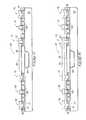
- a semiconductor wafer fragment 10comprises a bulk monocrystalline semiconductive substrate 12 and is shown in but one preferred embodiment of a method of forming integrated circuitry, for example integrated circuitry comprising voltage or current controlled resistance setable material.
- semiconductor substrateor “semiconductive substrate” is defined to mean any construction comprising semiconductive material, including, but not limited to, bulk semiconductive materials such as a semiconductive wafer (either alone or in assemblies comprising other materials thereon), and semiconductive material layers (either alone or in assemblies comprising other materials).
- substraterefers to any supporting structure, including, but not limited to, the semiconductive substrates described above.
- resistance setable materialincludes material wherein a property or properties in addition to resistance is/are also varied. For example, and by way of example only, the material's capacitance and/or inductance might also be changed in addition to resistance.
- FIG. 1depicts but one preferred implementation of the invention in a method of forming non-volatile random access memory circuitry.
- a plurality of memory cell access transistor gates 14 , 16 , 18 and 20are formed over semiconductor substrate 12 .
- suchcomprise a gate dielectric layer 22 , an overlying conductively doped polysilicon layer 24 , an overlying conductive metal silicide layer 26 , an insulative cap 28 , and opposing anisotropically etched insulative sidewall spacers 29 .
- gate constructions 14 - 20are in the form of memory cell wordlines.
- Substrate isolationfor example LOCOS field isolation oxide or trench isolation, is not shown for clarity, and as not constituting particular materiality to the invention. Discussion proceeds with processing particularly material to memory cell wordlines 16 and 18 which are proximate one another.
- a planarized insulating layer 30has been formed over the illustrated transistor gates and substrate 12 .
- An example preferred materialis borophosphosilicate glass (BPSG) deposited by chemical vapor deposition and planarized back by a polishing, for example chemical-mechanical polishing.
- Contact openings 32have been formed therein to semiconductive substrate 12 and filled with a conductive plugging material 34 .
- An example material for plugging material 34is conductively doped polysilicon.
- conductive metal or metal compound layersmight also be formed to constitute some or all of material 34 .
- Another insulative material layer 36has been deposited and planarized.
- BPSGis but one exemplary material for layer 36 .
- at least one of materials 30 and 36comprises a boron and/or phosphorus doped silicon dioxide glass comprising layer. Such can also be planarized or otherwise processed by reflow at a temperature of at least 750° C.
- a contact opening 38has been formed therethrough to the conductive plugging material 34 which is received between memory cell wordlines 16 and 18 .
- Suchhas been filled with a conductive plugging material 40 .
- Exemplary materials for material 40include conductively doped semiconductive materials, such as polysilicon, and metal or metal compounds, and mixtures thereof.
- At least one metal bit line 42is formed in electrical connection with material 40 as shown.
- bit line 42is formed in electrical connection with the active area of semiconductive substrate 12 located between memory cell wordlines 16 and 18 .
- metal bit linedefines a conductive bit line which includes at least one of, a) a conductive metal in elemental form; b) a conductive metal alloy comprising at least two elemental metals; and c) a conductive metal compound other than a silicide.
- exemplary elemental metals and alloys thereofinclude aluminum, copper, gold, silver, platinum, palladium and rhodium.
- exemplary metal compoundsinclude titanium nitride and conductive metal oxides, such as rhodium oxides.
- bit lines 42would typically be fabricated, with only one such bit line 42 being shown in the depicted cross-section.
- suchconstitutes the first metal layer formed over the substrate and, in some instances, is referred to as the Metal 1 layer by people of skill in the art.
- metal bit line 42constitutes a metal interconnect line which is formed over the substrate and memory cell access transistor gates.
- metal interconnect linedefines at least one conductive line which is not a transistor gate line and which electrically connects at least two devices and includes at least one of, a) a conductive metal in element form; b) a conductive metal alloy comprising at least two elemental metals; and c) a conductive metal compound other than a silicide.
- interconnect lines 42might also comprise a conductive metal silicide portion in addition to at least one of the materials referred to above. Examples include titanium silicides and tungsten silicides.
- interconnect lines 42might include any combination or mixtures of conductive elemental metals, metal alloys comprising at least two elemental metals, at least one conductive metal compound other than a silicide, and a conductive metal silicide. Further, the metal interconnect lines might consist essentially of any of these materials, alone or in combination.
- an interlevel dielectric layer 44is formed over dielectric layer 36 and metal interconnect lines/bit lines 42 .
- Exemplary materialsinclude undoped silicon dioxide and silicon nitride.
- Container openings 46are etched into insulating materials 44 and 36 to the conductive plugging material 34 which is received on respective lateral outer sides of wordlines 16 and 18 .
- Respective first memory cell electrodes 48are formed within container openings 46 and, accordingly, in electrical connection with active area of semiconductive substrate 12 on respective lateral outer sides of wordlines 16 and 18 . Accordingly, the exemplary respective first memory cell electrodes are formed in electrical connection with respective memory cell access transistors incorporating the illustrated memory cell access transistor gates. Source/drain regions (not shown) would be provided within or proximate semiconductive substrate 12 .
- Exemplary preferred materials for first electrodes 48include elemental metals, metal alloys and conductive metal compounds. Exemplary preferred materials include silver, for example silver in elemental or alloy form. Such material would preferably be deposited by physical or chemical vapor deposition, planarize polished back, and then recess etched to slightly below the outermost surface of interlevel dielectric layer 44 , as shown.
- a voltage or current controlled resistance setable semiconductive material 50is formed in electrical connection with the respective first at electrodes 48 .
- Exemplary resistance setable semiconductive materialincludes chalcogenide material having metal ions diffused therein.
- One exemplary materialcomprises Ge x A y , where “A” is selected from the group consisting of Se, Te, S, and mixtures thereof.
- Exemplary preferred metal ions within material 50include silver ions.
- An example preferred method for forming material 50is by chemical vapor deposition followed by a thin metal layer deposition thereon (i.e., preferably to less than 30% of the thickness of material 50 ).
- Exemplary preferred materials for the metalinclude silver and copper.
- Such metalis then preferably irradiated effective to break a chalcogenide bond of the chalcogenide material at an interface of such metal and chalcogenide material, and diffuse at least some of the metal into the chalcogenide material to diffuse metal ions therein.
- a preferred irradiatingincludes exposure to actinic radiation having a wavelength of from about 164-904 nanometers, with radiation exposure at between 404-408 nanometers being a more specific example.
- An even more specific exampleis a flood UV exposure tool operating at 4.5 milliwatts/cm 2 energy for 15 minutes in an oxygen-containing ambient at room temperature and pressure.
- the thickness of the metal layeris also preferably chosen to be suitably thin to enable the impinging electromagnetic radiation to essentially transparently pass through such metal to the interface of such metal with the chalcogenide material.
- Such layeris ultimately preferably planarized and recess etched back slightly relative to interlevel dielectric layer 44 , as shown.
- At least one second memory cell electrode 52is formed in electrical connection with voltage or current controlled resistance setable material 50 .
- second memory cell electrode 52is common to each of memory cells 54 and 56 , and preferably common to other memory cells which are formed.
- first memory cell electrodes, the resistance setable semiconductive material, and the second memory cell electrode(s)are formed into respective memory cell container shapes.
- the metal ions received within chalcogenide material 50include silver, and preferably at least one of the first and second electrodes comprises silver and more preferably silver in elemental form.
- the inventioncomprises a method of forming any memory circuitry which sequentially comprises the formation of some plurality of metal interconnect lines over a semiconductive substrate followed by the formation of a plurality of memory cell storage devices comprising voltage or current controlled resistance setable semiconductive material.
- the inventioncomprises any method of forming integrated circuitry (whether existing or yet-to-be-developed) which sequentially comprises forming at least one metal interconnect line over a semiconductive substrate followed by the formation of any device comprising two metal comprising electrodes separated by a voltage or current controlled resistance setable semiconductive material.
- FIG. 3depicts a wafer fragment 60 comprising a bulk semiconductive substrate 62 having an exemplary shallow trench field isolation region 64 formed therein.
- Various exemplary conductive device components 66 , 68 , 70 , 72 , 74 and 76are shown as being formed over substrate 62 .
- Suchmight constitute completed devices or devices in fabrication in the form of conductive lines, such as interconnect lines or field effect transistor lines, or any other conductive device or component thereof.
- such device componentsare depicted as having conductive polysilicon portions 77 , overlying metal portions 79 , and insulative silicon nitride caps 78 .
- a dielectric layer 80has been deposited, and planarized back.
- An exemplary silicon nitride layer 82is formed thereover.
- Exemplary contact openingshave been formed through layers 82 and 78 with respect to conductive device components 66 , 68 , 70 , 74 and 76 .
- a conductive layeris deposited and patterned to form at least one metal interconnect line 84 over the illustrated two conductive device components 70 and 72 .
- Suchis preferably formed by suitable metal, metals, or metal compound(s) deposition/formation, followed by photolithographic patterning and etch.
- Exemplary materials for the subject metal layerinclude tungsten nitride, tungsten, nickel, copper and mixtures thereof. Such provides but one example of forming a metal interconnect line over two conductive device components in the context of but one aspect of the invention.
- At least one opening 82is formed through metal interconnect line 84 to at least one of the two conductive device components, with only a single opening 82 being shown formed to conductive device component 72 .
- Preferred methods by which opening 82 is formedinclude photolithography and etching of metal interconnect line 80 .
- a preferred chalcogenide comprising material 85is deposited as shown. Such material is patterned, polished or etched back ( FIG. 7 ) by wet or dry processes. Metal ion insertion/doping thereof is preferably conducted as part of the FIG. 6 processing or as part of the FIG. 7 processing, and is preferably conducted by way of example only by metal layer irradiation as described above. Regardless, such provides but one example of forming voltage or current controlled resistance setable semiconductive material 85 within opening 82 in electrical connection with the respective one of the exemplary subject two device components 70 and 72 , with the depicted example showing such material being formed to only partially fill opening 82 .
- a conductive material 88is formed within opening 82 in electrical connection with resistance setable semiconductive material 85 and in electrical connection with metal interconnect line 84 .
- at least one of the conductive material 88 and that of device component 72comprises silver, and more preferably elemental silver. Any other alternate conductive material, whether existing or yet-to-be-developed, is also contemplated, of course.
- conductive material 88is formed to less than completely fill remaining portions of opening 82 , with a preferred container shape being formed as shown in FIG. 8 .
- Suchprovides but one example of forming voltage or current controlled resistance setable semiconductive material 84 within opening 82 in electrical connection with the respective one of the two device components and in electrical connection with metal interconnect line 84 with, in the depicted preferred embodiment, such being provided by the provision of a conductive material 88 .
Landscapes
- Engineering & Computer Science (AREA)
- Physics & Mathematics (AREA)
- Condensed Matter Physics & Semiconductors (AREA)
- General Physics & Mathematics (AREA)
- Manufacturing & Machinery (AREA)
- Computer Hardware Design (AREA)
- Microelectronics & Electronic Packaging (AREA)
- Power Engineering (AREA)
- Semiconductor Memories (AREA)
Abstract
Description
Claims (87)
Priority Applications (1)
| Application Number | Priority Date | Filing Date | Title |
|---|---|---|---|
| US09/921,518US6951805B2 (en) | 2001-08-01 | 2001-08-01 | Method of forming integrated circuitry, method of forming memory circuitry, and method of forming random access memory circuitry |
Applications Claiming Priority (1)
| Application Number | Priority Date | Filing Date | Title |
|---|---|---|---|
| US09/921,518US6951805B2 (en) | 2001-08-01 | 2001-08-01 | Method of forming integrated circuitry, method of forming memory circuitry, and method of forming random access memory circuitry |
Publications (2)
| Publication Number | Publication Date |
|---|---|
| US20030027416A1 US20030027416A1 (en) | 2003-02-06 |
| US6951805B2true US6951805B2 (en) | 2005-10-04 |
Family
ID=25445550
Family Applications (1)
| Application Number | Title | Priority Date | Filing Date |
|---|---|---|---|
| US09/921,518Expired - LifetimeUS6951805B2 (en) | 2001-08-01 | 2001-08-01 | Method of forming integrated circuitry, method of forming memory circuitry, and method of forming random access memory circuitry |
Country Status (1)
| Country | Link |
|---|---|
| US (1) | US6951805B2 (en) |
Cited By (7)
| Publication number | Priority date | Publication date | Assignee | Title |
|---|---|---|---|---|
| US20050030832A1 (en)* | 2002-09-03 | 2005-02-10 | Se-Ho Lee | Phase-changeable memory devices having phase-changeable material regions with lateral contacts and methods of fabrication therefor |
| US20060121726A1 (en)* | 2004-12-03 | 2006-06-08 | Micron Technology, Inc. | Methods of depositing silver onto a metal selenide-comprising surface, methods of depositing silver onto a selenium-comprising surface, and methods of forming a resistance variable device |
| US20070082492A1 (en)* | 2005-10-12 | 2007-04-12 | Samsung Electronics Co., Ltd. | Semiconductor memory device and method of fabricating the same |
| US20080144356A1 (en)* | 2006-12-13 | 2008-06-19 | Samsung Electronics Co., Ltd. | Nonvolatile memory devices having multi-filament variable resistivity memory cells therein |
| US20100032732A1 (en)* | 2008-08-06 | 2010-02-11 | International Business Machines Corporation | Electrical antifuse having a multi-thickness dielectric layer |
| US9006075B2 (en) | 2011-11-17 | 2015-04-14 | Micron Technology, Inc. | Memory cells, semiconductor devices including such cells, and methods of fabrication |
| US9048415B2 (en) | 2012-01-11 | 2015-06-02 | Micron Technology, Inc. | Memory cells including top electrodes comprising metal silicide, apparatuses including such cells, and related methods |
Families Citing this family (82)
| Publication number | Priority date | Publication date | Assignee | Title |
|---|---|---|---|---|
| US6653193B2 (en)* | 2000-12-08 | 2003-11-25 | Micron Technology, Inc. | Resistance variable device |
| US6638820B2 (en)* | 2001-02-08 | 2003-10-28 | Micron Technology, Inc. | Method of forming chalcogenide comprising devices, method of precluding diffusion of a metal into adjacent chalcogenide material, and chalcogenide comprising devices |
| JP4742429B2 (en)* | 2001-02-19 | 2011-08-10 | 住友電気工業株式会社 | Method for producing glass particulate deposit |
| US6727192B2 (en) | 2001-03-01 | 2004-04-27 | Micron Technology, Inc. | Methods of metal doping a chalcogenide material |
| US6818481B2 (en) | 2001-03-07 | 2004-11-16 | Micron Technology, Inc. | Method to manufacture a buried electrode PCRAM cell |
| US6734455B2 (en)* | 2001-03-15 | 2004-05-11 | Micron Technology, Inc. | Agglomeration elimination for metal sputter deposition of chalcogenides |
| US7102150B2 (en)* | 2001-05-11 | 2006-09-05 | Harshfield Steven T | PCRAM memory cell and method of making same |
| US6951805B2 (en) | 2001-08-01 | 2005-10-04 | Micron Technology, Inc. | Method of forming integrated circuitry, method of forming memory circuitry, and method of forming random access memory circuitry |
| US6737312B2 (en) | 2001-08-27 | 2004-05-18 | Micron Technology, Inc. | Method of fabricating dual PCRAM cells sharing a common electrode |
| US6881623B2 (en)* | 2001-08-29 | 2005-04-19 | Micron Technology, Inc. | Method of forming chalcogenide comprising devices, method of forming a programmable memory cell of memory circuitry, and a chalcogenide comprising device |
| US6784018B2 (en) | 2001-08-29 | 2004-08-31 | Micron Technology, Inc. | Method of forming chalcogenide comprising devices and method of forming a programmable memory cell of memory circuitry |
| US6955940B2 (en)* | 2001-08-29 | 2005-10-18 | Micron Technology, Inc. | Method of forming chalcogenide comprising devices |
| US6646902B2 (en) | 2001-08-30 | 2003-11-11 | Micron Technology, Inc. | Method of retaining memory state in a programmable conductor RAM |
| US6709958B2 (en) | 2001-08-30 | 2004-03-23 | Micron Technology, Inc. | Integrated circuit device and fabrication using metal-doped chalcogenide materials |
| US7109056B2 (en)* | 2001-09-20 | 2006-09-19 | Micron Technology, Inc. | Electro-and electroless plating of metal in the manufacture of PCRAM devices |
| US6815818B2 (en)* | 2001-11-19 | 2004-11-09 | Micron Technology, Inc. | Electrode structure for use in an integrated circuit |
| US6791859B2 (en) | 2001-11-20 | 2004-09-14 | Micron Technology, Inc. | Complementary bit PCRAM sense amplifier and method of operation |
| US6873538B2 (en)* | 2001-12-20 | 2005-03-29 | Micron Technology, Inc. | Programmable conductor random access memory and a method for writing thereto |
| US6909656B2 (en) | 2002-01-04 | 2005-06-21 | Micron Technology, Inc. | PCRAM rewrite prevention |
| US20030143782A1 (en)* | 2002-01-31 | 2003-07-31 | Gilton Terry L. | Methods of forming germanium selenide comprising devices and methods of forming silver selenide comprising structures |
| US6867064B2 (en)* | 2002-02-15 | 2005-03-15 | Micron Technology, Inc. | Method to alter chalcogenide glass for improved switching characteristics |
| US6791885B2 (en)* | 2002-02-19 | 2004-09-14 | Micron Technology, Inc. | Programmable conductor random access memory and method for sensing same |
| US6891749B2 (en)* | 2002-02-20 | 2005-05-10 | Micron Technology, Inc. | Resistance variable ‘on ’ memory |
| US7087919B2 (en)* | 2002-02-20 | 2006-08-08 | Micron Technology, Inc. | Layered resistance variable memory device and method of fabrication |
| US6847535B2 (en) | 2002-02-20 | 2005-01-25 | Micron Technology, Inc. | Removable programmable conductor memory card and associated read/write device and method of operation |
| US7151273B2 (en) | 2002-02-20 | 2006-12-19 | Micron Technology, Inc. | Silver-selenide/chalcogenide glass stack for resistance variable memory |
| US6809362B2 (en)* | 2002-02-20 | 2004-10-26 | Micron Technology, Inc. | Multiple data state memory cell |
| US6937528B2 (en) | 2002-03-05 | 2005-08-30 | Micron Technology, Inc. | Variable resistance memory and method for sensing same |
| US6849868B2 (en) | 2002-03-14 | 2005-02-01 | Micron Technology, Inc. | Methods and apparatus for resistance variable material cells |
| US6751114B2 (en) | 2002-03-28 | 2004-06-15 | Micron Technology, Inc. | Method for programming a memory cell |
| US6858482B2 (en) | 2002-04-10 | 2005-02-22 | Micron Technology, Inc. | Method of manufacture of programmable switching circuits and memory cells employing a glass layer |
| US6855975B2 (en)* | 2002-04-10 | 2005-02-15 | Micron Technology, Inc. | Thin film diode integrated with chalcogenide memory cell |
| US6864500B2 (en)* | 2002-04-10 | 2005-03-08 | Micron Technology, Inc. | Programmable conductor memory cell structure |
| US6731528B2 (en)* | 2002-05-03 | 2004-05-04 | Micron Technology, Inc. | Dual write cycle programmable conductor memory system and method of operation |
| US6825135B2 (en)* | 2002-06-06 | 2004-11-30 | Micron Technology, Inc. | Elimination of dendrite formation during metal/chalcogenide glass deposition |
| US6890790B2 (en)* | 2002-06-06 | 2005-05-10 | Micron Technology, Inc. | Co-sputter deposition of metal-doped chalcogenides |
| WO2004008535A1 (en)* | 2002-07-11 | 2004-01-22 | Matsushita Electric Industrial Co., Ltd. | Nonvolatile memory and its manufacturing method |
| US7209378B2 (en)* | 2002-08-08 | 2007-04-24 | Micron Technology, Inc. | Columnar 1T-N memory cell structure |
| US7018863B2 (en)* | 2002-08-22 | 2006-03-28 | Micron Technology, Inc. | Method of manufacture of a resistance variable memory cell |
| US7294527B2 (en) | 2002-08-29 | 2007-11-13 | Micron Technology Inc. | Method of forming a memory cell |
| US6867114B2 (en)* | 2002-08-29 | 2005-03-15 | Micron Technology Inc. | Methods to form a memory cell with metal-rich metal chalcogenide |
| US7163837B2 (en) | 2002-08-29 | 2007-01-16 | Micron Technology, Inc. | Method of forming a resistance variable memory element |
| US7010644B2 (en) | 2002-08-29 | 2006-03-07 | Micron Technology, Inc. | Software refreshed memory device and method |
| US6867996B2 (en)* | 2002-08-29 | 2005-03-15 | Micron Technology, Inc. | Single-polarity programmable resistance-variable memory element |
| US6864521B2 (en)* | 2002-08-29 | 2005-03-08 | Micron Technology, Inc. | Method to control silver concentration in a resistance variable memory element |
| US6831019B1 (en) | 2002-08-29 | 2004-12-14 | Micron Technology, Inc. | Plasma etching methods and methods of forming memory devices comprising a chalcogenide comprising layer received operably proximate conductive electrodes |
| US20040040837A1 (en)* | 2002-08-29 | 2004-03-04 | Mcteer Allen | Method of forming chalcogenide sputter target |
| US7364644B2 (en)* | 2002-08-29 | 2008-04-29 | Micron Technology, Inc. | Silver selenide film stoichiometry and morphology control in sputter deposition |
| US6903394B2 (en)* | 2002-11-27 | 2005-06-07 | Micron Technology, Inc. | CMOS imager with improved color response |
| US6813178B2 (en)* | 2003-03-12 | 2004-11-02 | Micron Technology, Inc. | Chalcogenide glass constant current device, and its method of fabrication and operation |
| US7022579B2 (en)* | 2003-03-14 | 2006-04-04 | Micron Technology, Inc. | Method for filling via with metal |
| US7050327B2 (en)* | 2003-04-10 | 2006-05-23 | Micron Technology, Inc. | Differential negative resistance memory |
| US6930909B2 (en) | 2003-06-25 | 2005-08-16 | Micron Technology, Inc. | Memory device and methods of controlling resistance variation and resistance profile drift |
| US6961277B2 (en) | 2003-07-08 | 2005-11-01 | Micron Technology, Inc. | Method of refreshing a PCRAM memory device |
| US7061004B2 (en)* | 2003-07-21 | 2006-06-13 | Micron Technology, Inc. | Resistance variable memory elements and methods of formation |
| US6903361B2 (en) | 2003-09-17 | 2005-06-07 | Micron Technology, Inc. | Non-volatile memory structure |
| US7583551B2 (en)* | 2004-03-10 | 2009-09-01 | Micron Technology, Inc. | Power management control and controlling memory refresh operations |
| US7098068B2 (en)* | 2004-03-10 | 2006-08-29 | Micron Technology, Inc. | Method of forming a chalcogenide material containing device |
| US7354793B2 (en)* | 2004-08-12 | 2008-04-08 | Micron Technology, Inc. | Method of forming a PCRAM device incorporating a resistance-variable chalocogenide element |
| US7190048B2 (en)* | 2004-07-19 | 2007-03-13 | Micron Technology, Inc. | Resistance variable memory device and method of fabrication |
| US7326950B2 (en)* | 2004-07-19 | 2008-02-05 | Micron Technology, Inc. | Memory device with switching glass layer |
| US7365411B2 (en) | 2004-08-12 | 2008-04-29 | Micron Technology, Inc. | Resistance variable memory with temperature tolerant materials |
| US7151688B2 (en)* | 2004-09-01 | 2006-12-19 | Micron Technology, Inc. | Sensing of resistance variable memory devices |
| US7224598B2 (en)* | 2004-09-02 | 2007-05-29 | Hewlett-Packard Development Company, L.P. | Programming of programmable resistive memory devices |
| US20060131555A1 (en)* | 2004-12-22 | 2006-06-22 | Micron Technology, Inc. | Resistance variable devices with controllable channels |
| US7374174B2 (en)* | 2004-12-22 | 2008-05-20 | Micron Technology, Inc. | Small electrode for resistance variable devices |
| US7317200B2 (en) | 2005-02-23 | 2008-01-08 | Micron Technology, Inc. | SnSe-based limited reprogrammable cell |
| US7269044B2 (en) | 2005-04-22 | 2007-09-11 | Micron Technology, Inc. | Method and apparatus for accessing a memory array |
| US7709289B2 (en) | 2005-04-22 | 2010-05-04 | Micron Technology, Inc. | Memory elements having patterned electrodes and method of forming the same |
| US7427770B2 (en) | 2005-04-22 | 2008-09-23 | Micron Technology, Inc. | Memory array for increased bit density |
| US7269079B2 (en) | 2005-05-16 | 2007-09-11 | Micron Technology, Inc. | Power circuits for reducing a number of power supply voltage taps required for sensing a resistive memory |
| US7233520B2 (en)* | 2005-07-08 | 2007-06-19 | Micron Technology, Inc. | Process for erasing chalcogenide variable resistance memory bits |
| US7274034B2 (en) | 2005-08-01 | 2007-09-25 | Micron Technology, Inc. | Resistance variable memory device with sputtered metal-chalcogenide region and method of fabrication |
| US7317567B2 (en)* | 2005-08-02 | 2008-01-08 | Micron Technology, Inc. | Method and apparatus for providing color changing thin film material |
| US7332735B2 (en)* | 2005-08-02 | 2008-02-19 | Micron Technology, Inc. | Phase change memory cell and method of formation |
| US20070037316A1 (en)* | 2005-08-09 | 2007-02-15 | Micron Technology, Inc. | Memory cell contact using spacers |
| US7579615B2 (en)* | 2005-08-09 | 2009-08-25 | Micron Technology, Inc. | Access transistor for memory device |
| US7304368B2 (en)* | 2005-08-11 | 2007-12-04 | Micron Technology, Inc. | Chalcogenide-based electrokinetic memory element and method of forming the same |
| US7251154B2 (en) | 2005-08-15 | 2007-07-31 | Micron Technology, Inc. | Method and apparatus providing a cross-point memory array using a variable resistance memory cell and capacitance |
| US7277313B2 (en)* | 2005-08-31 | 2007-10-02 | Micron Technology, Inc. | Resistance variable memory element with threshold device and method of forming the same |
| US7560723B2 (en)* | 2006-08-29 | 2009-07-14 | Micron Technology, Inc. | Enhanced memory density resistance variable memory cells, arrays, devices and systems including the same, and methods of fabrication |
| US8467236B2 (en)* | 2008-08-01 | 2013-06-18 | Boise State University | Continuously variable resistor |
Citations (184)
| Publication number | Priority date | Publication date | Assignee | Title |
|---|---|---|---|---|
| US3271591A (en) | 1963-09-20 | 1966-09-06 | Energy Conversion Devices Inc | Symmetrical current controlling device |
| US3622319A (en) | 1966-10-20 | 1971-11-23 | Western Electric Co | Nonreflecting photomasks and methods of making same |
| US3743847A (en) | 1971-06-01 | 1973-07-03 | Motorola Inc | Amorphous silicon film as a uv filter |
| US3961314A (en) | 1974-03-05 | 1976-06-01 | Energy Conversion Devices, Inc. | Structure and method for producing an image |
| US3966317A (en) | 1974-04-08 | 1976-06-29 | Energy Conversion Devices, Inc. | Dry process production of archival microform records from hard copy |
| US3983542A (en) | 1970-08-13 | 1976-09-28 | Energy Conversion Devices, Inc. | Method and apparatus for recording information |
| US4177474A (en) | 1977-05-18 | 1979-12-04 | Energy Conversion Devices, Inc. | High temperature amorphous semiconductor member and method of making the same |
| US4267261A (en) | 1971-07-15 | 1981-05-12 | Energy Conversion Devices, Inc. | Method for full format imaging |
| US4269935A (en) | 1979-07-13 | 1981-05-26 | Ionomet Company, Inc. | Process of doping silver image in chalcogenide layer |
| JPS56126916A (en) | 1980-03-10 | 1981-10-05 | Nippon Telegr & Teleph Corp <Ntt> | Manufacture of semiconductor device |
| US4312938A (en) | 1979-07-06 | 1982-01-26 | Drexler Technology Corporation | Method for making a broadband reflective laser recording and data storage medium with absorptive underlayer |
| US4316946A (en) | 1979-12-03 | 1982-02-23 | Ionomet Company, Inc. | Surface sensitized chalcogenide product and process for making and using the same |
| US4320191A (en) | 1978-11-07 | 1982-03-16 | Nippon Telegraph & Telephone Public Corporation | Pattern-forming process |
| US4405710A (en) | 1981-06-22 | 1983-09-20 | Cornell Research Foundation, Inc. | Ion beam exposure of (g-Gex -Se1-x) inorganic resists |
| US4419421A (en) | 1979-01-15 | 1983-12-06 | Max-Planck-Gesellschaft Zur Forderung Der Wissenschaften E.V. | Ion conductor material |
| US4499557A (en) | 1980-10-28 | 1985-02-12 | Energy Conversion Devices, Inc. | Programmable cell for use in programmable electronic arrays |
| US4597162A (en) | 1983-01-18 | 1986-07-01 | Energy Conversion Devices, Inc. | Method for making, parallel preprogramming or field programming of electronic matrix arrays |
| US4608296A (en) | 1983-12-06 | 1986-08-26 | Energy Conversion Devices, Inc. | Superconducting films and devices exhibiting AC to DC conversion |
| US4637895A (en) | 1985-04-01 | 1987-01-20 | Energy Conversion Devices, Inc. | Gas mixtures for the vapor deposition of semiconductor material |
| US4646266A (en) | 1984-09-28 | 1987-02-24 | Energy Conversion Devices, Inc. | Programmable semiconductor structures and methods for using the same |
| US4664939A (en) | 1985-04-01 | 1987-05-12 | Energy Conversion Devices, Inc. | Vertical semiconductor processor |
| US4668968A (en) | 1984-05-14 | 1987-05-26 | Energy Conversion Devices, Inc. | Integrated circuit compatible thin film field effect transistor and method of making same |
| US4670763A (en) | 1984-05-14 | 1987-06-02 | Energy Conversion Devices, Inc. | Thin film field effect transistor |
| US4671618A (en) | 1986-05-22 | 1987-06-09 | Wu Bao Gang | Liquid crystalline-plastic material having submillisecond switch times and extended memory |
| US4673957A (en) | 1984-05-14 | 1987-06-16 | Energy Conversion Devices, Inc. | Integrated circuit compatible thin film field effect transistor and method of making same |
| US4678679A (en) | 1984-06-25 | 1987-07-07 | Energy Conversion Devices, Inc. | Continuous deposition of activated process gases |
| US4710899A (en) | 1985-06-10 | 1987-12-01 | Energy Conversion Devices, Inc. | Data storage medium incorporating a transition metal for increased switching speed |
| US4728406A (en) | 1986-08-18 | 1988-03-01 | Energy Conversion Devices, Inc. | Method for plasma - coating a semiconductor body |
| US4737379A (en) | 1982-09-24 | 1988-04-12 | Energy Conversion Devices, Inc. | Plasma deposited coatings, and low temperature plasma method of making same |
| US4766471A (en) | 1986-01-23 | 1988-08-23 | Energy Conversion Devices, Inc. | Thin film electro-optical devices |
| US4769338A (en) | 1984-05-14 | 1988-09-06 | Energy Conversion Devices, Inc. | Thin film field effect transistor and method of making same |
| US4775425A (en) | 1987-07-27 | 1988-10-04 | Energy Conversion Devices, Inc. | P and n-type microcrystalline semiconductor alloy material including band gap widening elements, devices utilizing same |
| US4788594A (en) | 1986-10-15 | 1988-11-29 | Energy Conversion Devices, Inc. | Solid state electronic camera including thin film matrix of photosensors |
| US4795657A (en) | 1984-04-13 | 1989-01-03 | Energy Conversion Devices, Inc. | Method of fabricating a programmable array |
| US4800526A (en) | 1987-05-08 | 1989-01-24 | Gaf Corporation | Memory element for information storage and retrieval system and associated process |
| US4809044A (en) | 1986-08-22 | 1989-02-28 | Energy Conversion Devices, Inc. | Thin film overvoltage protection devices |
| US4818717A (en) | 1986-06-27 | 1989-04-04 | Energy Conversion Devices, Inc. | Method for making electronic matrix arrays |
| US4843443A (en) | 1984-05-14 | 1989-06-27 | Energy Conversion Devices, Inc. | Thin film field effect transistor and method of making same |
| US4845533A (en) | 1986-08-22 | 1989-07-04 | Energy Conversion Devices, Inc. | Thin film electrical devices with amorphous carbon electrodes and method of making same |
| US4847674A (en) | 1987-03-10 | 1989-07-11 | Advanced Micro Devices, Inc. | High speed interconnect system with refractory non-dogbone contacts and an active electromigration suppression mechanism |
| US4853785A (en) | 1986-10-15 | 1989-08-01 | Energy Conversion Devices, Inc. | Electronic camera including electronic signal storage cartridge |
| US4891330A (en) | 1987-07-27 | 1990-01-02 | Energy Conversion Devices, Inc. | Method of fabricating n-type and p-type microcrystalline semiconductor alloy material including band gap widening elements |
| US5128099A (en) | 1991-02-15 | 1992-07-07 | Energy Conversion Devices, Inc. | Congruent state changeable optical memory material and device |
| US5159661A (en) | 1990-10-05 | 1992-10-27 | Energy Conversion Devices, Inc. | Vertically interconnected parallel distributed processor |
| US5166758A (en) | 1991-01-18 | 1992-11-24 | Energy Conversion Devices, Inc. | Electrically erasable phase change memory |
| US5177567A (en) | 1991-07-19 | 1993-01-05 | Energy Conversion Devices, Inc. | Thin-film structure for chalcogenide electrical switching devices and process therefor |
| US5219788A (en) | 1991-02-25 | 1993-06-15 | Ibm Corporation | Bilayer metallization cap for photolithography |
| US5238862A (en) | 1992-03-18 | 1993-08-24 | Micron Technology, Inc. | Method of forming a stacked capacitor with striated electrode |
| US5272359A (en) | 1988-04-07 | 1993-12-21 | California Institute Of Technology | Reversible non-volatile switch based on a TCNQ charge transfer complex |
| US5296716A (en) | 1991-01-18 | 1994-03-22 | Energy Conversion Devices, Inc. | Electrically erasable, directly overwritable, multibit single cell memory elements and arrays fabricated therefrom |
| US5315131A (en) | 1990-11-22 | 1994-05-24 | Matsushita Electric Industrial Co., Ltd. | Electrically reprogrammable nonvolatile memory device |
| US5314772A (en) | 1990-10-09 | 1994-05-24 | Arizona Board Of Regents | High resolution, multi-layer resist for microlithography and method therefor |
| US5335219A (en) | 1991-01-18 | 1994-08-02 | Ovshinsky Stanford R | Homogeneous composition of microcrystalline semiconductor material, semiconductor devices and directly overwritable memory elements fabricated therefrom, and arrays fabricated from the memory elements |
| US5341328A (en) | 1991-01-18 | 1994-08-23 | Energy Conversion Devices, Inc. | Electrically erasable memory elements having reduced switching current requirements and increased write/erase cycle life |
| US5350484A (en) | 1992-09-08 | 1994-09-27 | Intel Corporation | Method for the anisotropic etching of metal films in the fabrication of interconnects |
| US5359205A (en) | 1991-11-07 | 1994-10-25 | Energy Conversion Devices, Inc. | Electrically erasable memory elements characterized by reduced current and improved thermal stability |
| US5360981A (en) | 1989-05-11 | 1994-11-01 | British Telecommunications Public Limited Company | Amorphous silicon memory |
| US5406509A (en) | 1991-01-18 | 1995-04-11 | Energy Conversion Devices, Inc. | Electrically erasable, directly overwritable, multibit single cell memory elements and arrays fabricated therefrom |
| US5414271A (en) | 1991-01-18 | 1995-05-09 | Energy Conversion Devices, Inc. | Electrically erasable memory elements having improved set resistance stability |
| US5500532A (en) | 1994-08-18 | 1996-03-19 | Arizona Board Of Regents | Personal electronic dosimeter |
| US5512328A (en) | 1992-08-07 | 1996-04-30 | Hitachi, Ltd. | Method for forming a pattern and forming a thin film used in pattern formation |
| US5512773A (en) | 1993-12-23 | 1996-04-30 | U.S. Philips Corporation | Switching element with memory provided with Schottky tunnelling barrier |
| US5534712A (en) | 1991-01-18 | 1996-07-09 | Energy Conversion Devices, Inc. | Electrically erasable memory elements characterized by reduced current and improved thermal stability |
| US5534711A (en) | 1991-01-18 | 1996-07-09 | Energy Conversion Devices, Inc. | Electrically erasable, directly overwritable, multibit single cell memory elements and arrays fabricated therefrom |
| US5536947A (en) | 1991-01-18 | 1996-07-16 | Energy Conversion Devices, Inc. | Electrically erasable, directly overwritable, multibit single cell memory element and arrays fabricated therefrom |
| US5543737A (en) | 1995-02-10 | 1996-08-06 | Energy Conversion Devices, Inc. | Logical operation circuit employing two-terminal chalcogenide switches |
| US5591501A (en) | 1995-12-20 | 1997-01-07 | Energy Conversion Devices, Inc. | Optical recording medium having a plurality of discrete phase change data recording points |
| US5596522A (en) | 1991-01-18 | 1997-01-21 | Energy Conversion Devices, Inc. | Homogeneous compositions of microcrystalline semiconductor material, semiconductor devices and directly overwritable memory elements fabricated therefrom, and arrays fabricated from the memory elements |
| US5687112A (en) | 1996-04-19 | 1997-11-11 | Energy Conversion Devices, Inc. | Multibit single cell memory element having tapered contact |
| US5694054A (en) | 1995-11-28 | 1997-12-02 | Energy Conversion Devices, Inc. | Integrated drivers for flat panel displays employing chalcogenide logic elements |
| US5714768A (en) | 1995-10-24 | 1998-02-03 | Energy Conversion Devices, Inc. | Second-layer phase change memory array on top of a logic device |
| US5726083A (en)* | 1994-11-29 | 1998-03-10 | Nec Corporation | Process of fabricating dynamic random access memory device having storage capacitor low in contact resistance and small in leakage current through tantalum oxide film |
| US5751012A (en) | 1995-06-07 | 1998-05-12 | Micron Technology, Inc. | Polysilicon pillar diode for use in a non-volatile memory cell |
| US5761115A (en) | 1996-05-30 | 1998-06-02 | Axon Technologies Corporation | Programmable metallization cell structure and method of making same |
| US5789277A (en) | 1996-07-22 | 1998-08-04 | Micron Technology, Inc. | Method of making chalogenide memory device |
| US5814527A (en) | 1996-07-22 | 1998-09-29 | Micron Technology, Inc. | Method of making small pores defined by a disposable internal spacer for use in chalcogenide memories |
| US5818749A (en) | 1993-08-20 | 1998-10-06 | Micron Technology, Inc. | Integrated circuit memory device |
| US5825046A (en) | 1996-10-28 | 1998-10-20 | Energy Conversion Devices, Inc. | Composite memory material comprising a mixture of phase-change memory material and dielectric material |
| US5841150A (en) | 1995-06-07 | 1998-11-24 | Micron Technology, Inc. | Stack/trench diode for use with a muti-state material in a non-volatile memory cell |
| US5846889A (en) | 1997-03-14 | 1998-12-08 | The United States Of America As Represented By The Secretary Of The Navy | Infrared transparent selenide glasses |
| US5851882A (en) | 1996-05-06 | 1998-12-22 | Micron Technology, Inc. | ZPROM manufacture and design and methods for forming thin structures using spacers as an etching mask |
| US5869843A (en) | 1995-06-07 | 1999-02-09 | Micron Technology, Inc. | Memory array having a multi-state element and method for forming such array or cells thereof |
| WO1999028914A2 (en) | 1997-12-04 | 1999-06-10 | Axon Technologies Corporation | Programmable sub-surface aggregating metallization structure and method of making same |
| US5912839A (en) | 1998-06-23 | 1999-06-15 | Energy Conversion Devices, Inc. | Universal memory element and method of programming same |
| US5920788A (en) | 1995-06-07 | 1999-07-06 | Micron Technology, Inc. | Chalcogenide memory cell with a plurality of chalcogenide electrodes |
| US5933365A (en) | 1997-06-19 | 1999-08-03 | Energy Conversion Devices, Inc. | Memory element with energy control mechanism |
| US5998066A (en) | 1997-05-16 | 1999-12-07 | Aerial Imaging Corporation | Gray scale mask and depth pattern transfer technique using inorganic chalcogenide glass |
| US6011757A (en) | 1998-01-27 | 2000-01-04 | Ovshinsky; Stanford R. | Optical recording media having increased erasability |
| US6031287A (en) | 1997-06-18 | 2000-02-29 | Micron Technology, Inc. | Contact structure and memory element incorporating the same |
| US6072716A (en) | 1999-04-14 | 2000-06-06 | Massachusetts Institute Of Technology | Memory structures and methods of making same |
| US6087674A (en) | 1996-10-28 | 2000-07-11 | Energy Conversion Devices, Inc. | Memory element with memory material comprising phase-change material and dielectric material |
| WO2000048196A1 (en) | 1999-02-11 | 2000-08-17 | Arizona Board Of Regents | Programmable microelectronic devices and methods of forming and programming same |
| US6117720A (en) | 1995-06-07 | 2000-09-12 | Micron Technology, Inc. | Method of making an integrated circuit electrode having a reduced contact area |
| US6141241A (en) | 1998-06-23 | 2000-10-31 | Energy Conversion Devices, Inc. | Universal memory element with systems employing same and apparatus and method for reading, writing and programming same |
| US6143604A (en)* | 1999-06-04 | 2000-11-07 | Taiwan Semiconductor Manufacturing Company | Method for fabricating small-size two-step contacts for word-line strapping on dynamic random access memory (DRAM) |
| US6177338B1 (en)* | 1999-02-08 | 2001-01-23 | Taiwan Semiconductor Manufacturing Company | Two step barrier process |
| US6236059B1 (en) | 1996-08-22 | 2001-05-22 | Micron Technology, Inc. | Memory cell incorporating a chalcogenide element and method of making same |
| US6297170B1 (en) | 1998-06-23 | 2001-10-02 | Vlsi Technology, Inc. | Sacrificial multilayer anti-reflective coating for mos gate formation |
| US6300684B1 (en) | 1995-06-07 | 2001-10-09 | Micron Technology, Inc. | Method for fabricating an array of ultra-small pores for chalcogenide memory cells |
| US6329606B1 (en) | 1996-04-24 | 2001-12-11 | Amkor Technology, Inc. | Grid array assembly of circuit boards with singulation grooves |
| US20020000666A1 (en) | 1998-08-31 | 2002-01-03 | Michael N. Kozicki | Self-repairing interconnections for electrical circuits |
| US6339544B1 (en) | 2000-09-29 | 2002-01-15 | Intel Corporation | Method to enhance performance of thermal resistor device |
| US6348365B1 (en) | 2001-03-02 | 2002-02-19 | Micron Technology, Inc. | PCRAM cell manufacturing |
| US6350679B1 (en)* | 1999-08-03 | 2002-02-26 | Micron Technology, Inc. | Methods of providing an interlevel dielectric layer intermediate different elevation conductive metal layers in the fabrication of integrated circuitry |
| WO2002021542A1 (en) | 2000-09-08 | 2002-03-14 | Axon Technologies Corporation | Microelectronic programmable device and methods of forming and programming the same |
| US6376284B1 (en) | 1996-02-23 | 2002-04-23 | Micron Technology, Inc. | Method of fabricating a memory device |
| US6404665B1 (en) | 2000-09-29 | 2002-06-11 | Intel Corporation | Compositionally modified resistive electrode |
| US20020072188A1 (en) | 2000-12-08 | 2002-06-13 | Gilton Terry L. | Non-volatile resistance variable devices and method of forming same, analog memory devices and method of forming same, programmable memory cell and method of forming same, and method of structurally changing a non-volatile device |
| US6414376B1 (en) | 1997-07-31 | 2002-07-02 | Micron Technology, Inc. | Method and apparatus for reducing isolation stress in integrated circuits |
| US6423628B1 (en) | 1999-10-22 | 2002-07-23 | Lsi Logic Corporation | Method of forming integrated circuit structure having low dielectric constant material and having silicon oxynitride caps over closely spaced apart metal lines |
| US6429064B1 (en) | 2000-09-29 | 2002-08-06 | Intel Corporation | Reduced contact area of sidewall conductor |
| US20020106849A1 (en) | 2001-02-08 | 2002-08-08 | Moore John T. | Method of forming non-volatile resistance variable devices, method of precluding diffusion of a metal into adjacent chalcogenide material, and non-volatile resistance variable devices |
| US6437383B1 (en) | 2000-12-21 | 2002-08-20 | Intel Corporation | Dual trench isolation for a phase-change memory cell and method of making same |
| US6440837B1 (en) | 2000-07-14 | 2002-08-27 | Micron Technology, Inc. | Method of forming a contact structure in a semiconductor device |
| US20020123169A1 (en) | 2001-03-01 | 2002-09-05 | Moore John T. | Methods of forming non-volatile resistance variable devices, and non-volatile resistance variable devices |
| US20020127886A1 (en) | 2001-03-07 | 2002-09-12 | Moore John T. | Method to manufacture a buried electrode PCRAM cell |
| US20020132417A1 (en) | 2001-03-15 | 2002-09-19 | Jiutao Li | Agglomeration elimination for metal sputter deposition of chalcogenides |
| US6462984B1 (en) | 2001-06-29 | 2002-10-08 | Intel Corporation | Biasing scheme of floating unselected wordlines and bitlines of a diode-based memory array |
| US6469364B1 (en) | 1998-08-31 | 2002-10-22 | Arizona Board Of Regents | Programmable interconnection system for electrical circuits |
| US6473332B1 (en) | 2001-04-04 | 2002-10-29 | The University Of Houston System | Electrically variable multi-state resistance computing |
| US20020160551A1 (en) | 2001-03-15 | 2002-10-31 | Harshfield Steven T. | Memory elements and methods for making same |
| US20020163828A1 (en) | 2001-05-07 | 2002-11-07 | Coatue Corporation | Memory device with a self-assembled polymer film and method of making the same |
| US6480438B1 (en) | 2001-06-12 | 2002-11-12 | Ovonyx, Inc. | Providing equal cell programming conditions across a large and high density array of phase-change memory cells |
| US20020168852A1 (en) | 2001-05-11 | 2002-11-14 | Harshfield Steven T. | PCRAM memory cell and method of making same |
| US20020168820A1 (en) | 2000-09-08 | 2002-11-14 | Kozicki Michael N. | Microelectronic programmable device and methods of forming and programming the same |
| US6487106B1 (en) | 1999-01-12 | 2002-11-26 | Arizona Board Of Regents | Programmable microelectronic devices and method of forming and programming same |
| US6487113B1 (en) | 2001-06-29 | 2002-11-26 | Ovonyx, Inc. | Programming a phase-change memory with slow quench time |
| US6501111B1 (en) | 2000-06-30 | 2002-12-31 | Intel Corporation | Three-dimensional (3D) programmable device |
| US6507061B1 (en) | 2001-08-31 | 2003-01-14 | Intel Corporation | Multiple layer phase-change memory |
| US6511862B2 (en) | 2001-06-30 | 2003-01-28 | Ovonyx, Inc. | Modified contact for programmable devices |
| US6512241B1 (en) | 2001-12-31 | 2003-01-28 | Intel Corporation | Phase change material memory device |
| US6511867B2 (en) | 2001-06-30 | 2003-01-28 | Ovonyx, Inc. | Utilizing atomic layer deposition for programmable device |
| US6514805B2 (en) | 2001-06-30 | 2003-02-04 | Intel Corporation | Trench sidewall profile for device isolation |
| US20030027416A1 (en) | 2001-08-01 | 2003-02-06 | Moore John T. | Method of forming integrated circuitry, method of forming memory circuitry, and method of forming random access memory circuitry |
| US20030035315A1 (en) | 2001-04-06 | 2003-02-20 | Kozicki Michael N. | Microelectronic device, structure, and system, including a memory structure having a variable programmable property and method of forming the same |
| US20030038301A1 (en) | 2001-08-27 | 2003-02-27 | John Moore | Apparatus and method for dual cell common electrode PCRAM memory device |
| US20030045049A1 (en) | 2001-08-29 | 2003-03-06 | Campbell Kristy A. | Method of forming chalcogenide comprising devices |
| US20030045054A1 (en) | 2001-08-29 | 2003-03-06 | Campbell Kristy A. | Method of forming non-volatile resistance variable devices, method of forming a programmable memory cell of memory circuitry, and a non-volatile resistance variable device |
| US20030043631A1 (en) | 2001-08-30 | 2003-03-06 | Gilton Terry L. | Method of retaining memory state in a programmable conductor RAM |
| US6531373B2 (en) | 2000-12-27 | 2003-03-11 | Ovonyx, Inc. | Method of forming a phase-change memory cell using silicon on insulator low electrode in charcogenide elements |
| US20030049912A1 (en) | 2001-08-29 | 2003-03-13 | Campbell Kristy A. | Method of forming chalcogenide comprsing devices and method of forming a programmable memory cell of memory circuitry |
| US20030048519A1 (en) | 2000-02-11 | 2003-03-13 | Kozicki Michael N. | Microelectronic photonic structure and device and method of forming the same |
| US20030047765A1 (en) | 2001-08-30 | 2003-03-13 | Campbell Kristy A. | Stoichiometry for chalcogenide glasses useful for memory devices and method of formation |
| US20030048744A1 (en) | 2001-09-01 | 2003-03-13 | Ovshinsky Stanford R. | Increased data storage in optical data storage and retrieval systems using blue lasers and/or plasmon lenses |
| US6534781B2 (en) | 2000-12-26 | 2003-03-18 | Ovonyx, Inc. | Phase-change memory bipolar array utilizing a single shallow trench isolation for creating an individual active area region for two memory array elements and one bipolar base contact |
| US6545907B1 (en) | 2001-10-30 | 2003-04-08 | Ovonyx, Inc. | Technique and apparatus for performing write operations to a phase change material memory device |
| US6545287B2 (en) | 2001-09-07 | 2003-04-08 | Intel Corporation | Using selective deposition to form phase-change memory cells |
| US20030068862A1 (en) | 2001-08-30 | 2003-04-10 | Jiutao Li | Integrated circuit device and fabrication using metal-doped chalcogenide materials |
| US6555860B2 (en) | 2000-09-29 | 2003-04-29 | Intel Corporation | Compositionally modified resistive electrode |
| US6563164B2 (en) | 2000-09-29 | 2003-05-13 | Ovonyx, Inc. | Compositionally modified resistive electrode |
| US6566700B2 (en) | 2001-10-11 | 2003-05-20 | Ovonyx, Inc. | Carbon-containing interfacial layer for phase-change memory |
| US6567293B1 (en) | 2000-09-29 | 2003-05-20 | Ovonyx, Inc. | Single level metal memory cell using chalcogenide cladding |
| US20030095426A1 (en) | 2001-11-20 | 2003-05-22 | Glen Hush | Complementary bit PCRAM sense amplifier and method of operation |
| US20030096497A1 (en) | 2001-11-19 | 2003-05-22 | Micron Technology, Inc. | Electrode structure for use in an integrated circuit |
| US6570784B2 (en) | 2001-06-29 | 2003-05-27 | Ovonyx, Inc. | Programming a phase-change material memory |
| US6569705B2 (en) | 2000-12-21 | 2003-05-27 | Intel Corporation | Metal structure for a phase-change memory device |
| US6576921B2 (en) | 2001-11-08 | 2003-06-10 | Intel Corporation | Isolating phase change material memory cells |
| US20030107105A1 (en) | 1999-08-31 | 2003-06-12 | Kozicki Michael N. | Programmable chip-to-substrate interconnect structure and device and method of forming same |
| US20030117831A1 (en) | 2001-12-20 | 2003-06-26 | Glen Hush | Programmable conductor random access memory and a method for writing thereto |
| US6586761B2 (en) | 2001-09-07 | 2003-07-01 | Intel Corporation | Phase change material memory device |
| US6590807B2 (en) | 2001-08-02 | 2003-07-08 | Intel Corporation | Method for reading a structural phase-change memory |
| US6589714B2 (en) | 2001-06-26 | 2003-07-08 | Ovonyx, Inc. | Method for making programmable resistance memory element using silylated photoresist |
| US20030128612A1 (en) | 2002-01-04 | 2003-07-10 | John Moore | PCRAM rewrite prevention |
| US20030137869A1 (en) | 1998-12-04 | 2003-07-24 | Kozicki Michael N. | Programmable microelectronic device, structure, and system and method of forming the same |
| US20030143782A1 (en) | 2002-01-31 | 2003-07-31 | Gilton Terry L. | Methods of forming germanium selenide comprising devices and methods of forming silver selenide comprising structures |
| US6605527B2 (en) | 2001-06-30 | 2003-08-12 | Intel Corporation | Reduced area intersection between electrode and programming element |
| US20030156463A1 (en) | 2002-02-19 | 2003-08-21 | Casper Stephen L. | Programmable conductor random access memory and method for sensing same |
| US20030155589A1 (en) | 2002-02-20 | 2003-08-21 | Campbell Kristy A. | Silver-selenide/chalcogenide glass stack for resistance variable memory |
| US20030155606A1 (en) | 2002-02-15 | 2003-08-21 | Campbell Kristy A. | Method to alter chalcogenide glass for improved switching characteristics |
| US20030156447A1 (en) | 2000-02-11 | 2003-08-21 | Kozicki Michael N. | Programming circuit for a programmable microelectronic device, system including the circuit, and method of forming the same |
| US6613604B2 (en) | 2001-08-02 | 2003-09-02 | Ovonyx, Inc. | Method for making small pore for use in programmable resistance memory element |
| US6625054B2 (en) | 2001-12-28 | 2003-09-23 | Intel Corporation | Method and apparatus to program a phase change memory |
| US6642102B2 (en) | 2001-06-30 | 2003-11-04 | Intel Corporation | Barrier material encapsulation of programmable material |
| US6646297B2 (en) | 2000-12-26 | 2003-11-11 | Ovonyx, Inc. | Lower electrode isolation in a double-wide trench |
| US20030212724A1 (en) | 2002-05-10 | 2003-11-13 | Ovshinsky Stanford R. | Methods of computing with digital multistate phase change materials |
| US20030209971A1 (en) | 2000-02-11 | 2003-11-13 | Kozicki Michael N. | Programmable structure, an array including the structure, and methods of forming the same |
| US20030210564A1 (en) | 2001-10-26 | 2003-11-13 | Kozicki Michael N. | Tunable cantilever apparatus and method for making same |
| US6649928B2 (en) | 2000-12-13 | 2003-11-18 | Intel Corporation | Method to selectively remove one side of a conductive bottom electrode of a phase-change memory cell and structure obtained thereby |
| US6667900B2 (en) | 2001-12-28 | 2003-12-23 | Ovonyx, Inc. | Method and apparatus to operate a memory cell |
| US6673700B2 (en) | 2001-06-30 | 2004-01-06 | Ovonyx, Inc. | Reduced area intersection between electrode and programming element |
| US6687427B2 (en) | 2000-12-29 | 2004-02-03 | Intel Corporation | Optic switch |
| US6690026B2 (en) | 2001-09-28 | 2004-02-10 | Intel Corporation | Method of fabricating a three-dimensional array of active media |
| US6696355B2 (en) | 2000-12-14 | 2004-02-24 | Ovonyx, Inc. | Method to selectively increase the top resistance of the lower programming electrode in a phase-change memory |
| US20040035401A1 (en) | 2002-08-26 | 2004-02-26 | Subramanian Ramachandran | Hydrogen powered scooter |
- 2001
- 2001-08-01USUS09/921,518patent/US6951805B2/ennot_activeExpired - Lifetime
Patent Citations (220)
| Publication number | Priority date | Publication date | Assignee | Title |
|---|---|---|---|---|
| US3271591A (en) | 1963-09-20 | 1966-09-06 | Energy Conversion Devices Inc | Symmetrical current controlling device |
| US3622319A (en) | 1966-10-20 | 1971-11-23 | Western Electric Co | Nonreflecting photomasks and methods of making same |
| US3983542A (en) | 1970-08-13 | 1976-09-28 | Energy Conversion Devices, Inc. | Method and apparatus for recording information |
| US3988720A (en) | 1970-08-13 | 1976-10-26 | Energy Conversion Devices, Inc. | Recording and retrieving information in an amorphous memory material using a catalytic material |
| US3743847A (en) | 1971-06-01 | 1973-07-03 | Motorola Inc | Amorphous silicon film as a uv filter |
| US4267261A (en) | 1971-07-15 | 1981-05-12 | Energy Conversion Devices, Inc. | Method for full format imaging |
| US3961314A (en) | 1974-03-05 | 1976-06-01 | Energy Conversion Devices, Inc. | Structure and method for producing an image |
| US3966317A (en) | 1974-04-08 | 1976-06-29 | Energy Conversion Devices, Inc. | Dry process production of archival microform records from hard copy |
| US4177474A (en) | 1977-05-18 | 1979-12-04 | Energy Conversion Devices, Inc. | High temperature amorphous semiconductor member and method of making the same |
| US4320191A (en) | 1978-11-07 | 1982-03-16 | Nippon Telegraph & Telephone Public Corporation | Pattern-forming process |
| US4419421A (en) | 1979-01-15 | 1983-12-06 | Max-Planck-Gesellschaft Zur Forderung Der Wissenschaften E.V. | Ion conductor material |
| US4312938A (en) | 1979-07-06 | 1982-01-26 | Drexler Technology Corporation | Method for making a broadband reflective laser recording and data storage medium with absorptive underlayer |
| US4269935A (en) | 1979-07-13 | 1981-05-26 | Ionomet Company, Inc. | Process of doping silver image in chalcogenide layer |
| US4316946A (en) | 1979-12-03 | 1982-02-23 | Ionomet Company, Inc. | Surface sensitized chalcogenide product and process for making and using the same |
| JPS56126916A (en) | 1980-03-10 | 1981-10-05 | Nippon Telegr & Teleph Corp <Ntt> | Manufacture of semiconductor device |
| US4499557A (en) | 1980-10-28 | 1985-02-12 | Energy Conversion Devices, Inc. | Programmable cell for use in programmable electronic arrays |
| US4405710A (en) | 1981-06-22 | 1983-09-20 | Cornell Research Foundation, Inc. | Ion beam exposure of (g-Gex -Se1-x) inorganic resists |
| US4737379A (en) | 1982-09-24 | 1988-04-12 | Energy Conversion Devices, Inc. | Plasma deposited coatings, and low temperature plasma method of making same |
| US4597162A (en) | 1983-01-18 | 1986-07-01 | Energy Conversion Devices, Inc. | Method for making, parallel preprogramming or field programming of electronic matrix arrays |
| US4608296A (en) | 1983-12-06 | 1986-08-26 | Energy Conversion Devices, Inc. | Superconducting films and devices exhibiting AC to DC conversion |
| US4795657A (en) | 1984-04-13 | 1989-01-03 | Energy Conversion Devices, Inc. | Method of fabricating a programmable array |
| US4673957A (en) | 1984-05-14 | 1987-06-16 | Energy Conversion Devices, Inc. | Integrated circuit compatible thin film field effect transistor and method of making same |
| US4769338A (en) | 1984-05-14 | 1988-09-06 | Energy Conversion Devices, Inc. | Thin film field effect transistor and method of making same |
| US4670763A (en) | 1984-05-14 | 1987-06-02 | Energy Conversion Devices, Inc. | Thin film field effect transistor |
| US4843443A (en) | 1984-05-14 | 1989-06-27 | Energy Conversion Devices, Inc. | Thin film field effect transistor and method of making same |
| US4668968A (en) | 1984-05-14 | 1987-05-26 | Energy Conversion Devices, Inc. | Integrated circuit compatible thin film field effect transistor and method of making same |
| US4678679A (en) | 1984-06-25 | 1987-07-07 | Energy Conversion Devices, Inc. | Continuous deposition of activated process gases |
| US4646266A (en) | 1984-09-28 | 1987-02-24 | Energy Conversion Devices, Inc. | Programmable semiconductor structures and methods for using the same |
| US4637895A (en) | 1985-04-01 | 1987-01-20 | Energy Conversion Devices, Inc. | Gas mixtures for the vapor deposition of semiconductor material |
| US4696758A (en) | 1985-04-01 | 1987-09-29 | Energy Conversion Devices, Inc. | Gas mixtures for the vapor deposition of semiconductor material |
| US4698234A (en) | 1985-04-01 | 1987-10-06 | Energy Conversion Devices, Inc. | Vapor deposition of semiconductor material |
| US4664939A (en) | 1985-04-01 | 1987-05-12 | Energy Conversion Devices, Inc. | Vertical semiconductor processor |
| US4710899A (en) | 1985-06-10 | 1987-12-01 | Energy Conversion Devices, Inc. | Data storage medium incorporating a transition metal for increased switching speed |
| US4766471A (en) | 1986-01-23 | 1988-08-23 | Energy Conversion Devices, Inc. | Thin film electro-optical devices |
| US4671618A (en) | 1986-05-22 | 1987-06-09 | Wu Bao Gang | Liquid crystalline-plastic material having submillisecond switch times and extended memory |
| US4818717A (en) | 1986-06-27 | 1989-04-04 | Energy Conversion Devices, Inc. | Method for making electronic matrix arrays |
| US4728406A (en) | 1986-08-18 | 1988-03-01 | Energy Conversion Devices, Inc. | Method for plasma - coating a semiconductor body |
| US4845533A (en) | 1986-08-22 | 1989-07-04 | Energy Conversion Devices, Inc. | Thin film electrical devices with amorphous carbon electrodes and method of making same |
| US4809044A (en) | 1986-08-22 | 1989-02-28 | Energy Conversion Devices, Inc. | Thin film overvoltage protection devices |
| US4788594A (en) | 1986-10-15 | 1988-11-29 | Energy Conversion Devices, Inc. | Solid state electronic camera including thin film matrix of photosensors |
| US4853785A (en) | 1986-10-15 | 1989-08-01 | Energy Conversion Devices, Inc. | Electronic camera including electronic signal storage cartridge |
| US4847674A (en) | 1987-03-10 | 1989-07-11 | Advanced Micro Devices, Inc. | High speed interconnect system with refractory non-dogbone contacts and an active electromigration suppression mechanism |
| US4800526A (en) | 1987-05-08 | 1989-01-24 | Gaf Corporation | Memory element for information storage and retrieval system and associated process |
| US4891330A (en) | 1987-07-27 | 1990-01-02 | Energy Conversion Devices, Inc. | Method of fabricating n-type and p-type microcrystalline semiconductor alloy material including band gap widening elements |
| US4775425A (en) | 1987-07-27 | 1988-10-04 | Energy Conversion Devices, Inc. | P and n-type microcrystalline semiconductor alloy material including band gap widening elements, devices utilizing same |
| US5272359A (en) | 1988-04-07 | 1993-12-21 | California Institute Of Technology | Reversible non-volatile switch based on a TCNQ charge transfer complex |
| US5360981A (en) | 1989-05-11 | 1994-11-01 | British Telecommunications Public Limited Company | Amorphous silicon memory |
| US5159661A (en) | 1990-10-05 | 1992-10-27 | Energy Conversion Devices, Inc. | Vertically interconnected parallel distributed processor |
| US5314772A (en) | 1990-10-09 | 1994-05-24 | Arizona Board Of Regents | High resolution, multi-layer resist for microlithography and method therefor |
| US5315131A (en) | 1990-11-22 | 1994-05-24 | Matsushita Electric Industrial Co., Ltd. | Electrically reprogrammable nonvolatile memory device |
| US5166758A (en) | 1991-01-18 | 1992-11-24 | Energy Conversion Devices, Inc. | Electrically erasable phase change memory |
| US5414271A (en) | 1991-01-18 | 1995-05-09 | Energy Conversion Devices, Inc. | Electrically erasable memory elements having improved set resistance stability |
| US5296716A (en) | 1991-01-18 | 1994-03-22 | Energy Conversion Devices, Inc. | Electrically erasable, directly overwritable, multibit single cell memory elements and arrays fabricated therefrom |
| US5596522A (en) | 1991-01-18 | 1997-01-21 | Energy Conversion Devices, Inc. | Homogeneous compositions of microcrystalline semiconductor material, semiconductor devices and directly overwritable memory elements fabricated therefrom, and arrays fabricated from the memory elements |
| US5536947A (en) | 1991-01-18 | 1996-07-16 | Energy Conversion Devices, Inc. | Electrically erasable, directly overwritable, multibit single cell memory element and arrays fabricated therefrom |
| US5335219A (en) | 1991-01-18 | 1994-08-02 | Ovshinsky Stanford R | Homogeneous composition of microcrystalline semiconductor material, semiconductor devices and directly overwritable memory elements fabricated therefrom, and arrays fabricated from the memory elements |
| US5341328A (en) | 1991-01-18 | 1994-08-23 | Energy Conversion Devices, Inc. | Electrically erasable memory elements having reduced switching current requirements and increased write/erase cycle life |
| US5534711A (en) | 1991-01-18 | 1996-07-09 | Energy Conversion Devices, Inc. | Electrically erasable, directly overwritable, multibit single cell memory elements and arrays fabricated therefrom |
| US5534712A (en) | 1991-01-18 | 1996-07-09 | Energy Conversion Devices, Inc. | Electrically erasable memory elements characterized by reduced current and improved thermal stability |
| US5406509A (en) | 1991-01-18 | 1995-04-11 | Energy Conversion Devices, Inc. | Electrically erasable, directly overwritable, multibit single cell memory elements and arrays fabricated therefrom |
| US5128099A (en) | 1991-02-15 | 1992-07-07 | Energy Conversion Devices, Inc. | Congruent state changeable optical memory material and device |
| US5219788A (en) | 1991-02-25 | 1993-06-15 | Ibm Corporation | Bilayer metallization cap for photolithography |
| US5177567A (en) | 1991-07-19 | 1993-01-05 | Energy Conversion Devices, Inc. | Thin-film structure for chalcogenide electrical switching devices and process therefor |
| US5359205A (en) | 1991-11-07 | 1994-10-25 | Energy Conversion Devices, Inc. | Electrically erasable memory elements characterized by reduced current and improved thermal stability |
| US5238862A (en) | 1992-03-18 | 1993-08-24 | Micron Technology, Inc. | Method of forming a stacked capacitor with striated electrode |
| US5512328A (en) | 1992-08-07 | 1996-04-30 | Hitachi, Ltd. | Method for forming a pattern and forming a thin film used in pattern formation |
| US5350484A (en) | 1992-09-08 | 1994-09-27 | Intel Corporation | Method for the anisotropic etching of metal films in the fabrication of interconnects |
| US5818749A (en) | 1993-08-20 | 1998-10-06 | Micron Technology, Inc. | Integrated circuit memory device |
| US5512773A (en) | 1993-12-23 | 1996-04-30 | U.S. Philips Corporation | Switching element with memory provided with Schottky tunnelling barrier |
| US5500532A (en) | 1994-08-18 | 1996-03-19 | Arizona Board Of Regents | Personal electronic dosimeter |
| US5726083A (en)* | 1994-11-29 | 1998-03-10 | Nec Corporation | Process of fabricating dynamic random access memory device having storage capacitor low in contact resistance and small in leakage current through tantalum oxide film |
| US5543737A (en) | 1995-02-10 | 1996-08-06 | Energy Conversion Devices, Inc. | Logical operation circuit employing two-terminal chalcogenide switches |
| US5841150A (en) | 1995-06-07 | 1998-11-24 | Micron Technology, Inc. | Stack/trench diode for use with a muti-state material in a non-volatile memory cell |
| US6077729A (en) | 1995-06-07 | 2000-06-20 | Micron Technology, Inc. | Memory array having a multi-state element and method for forming such array or cellis thereof |
| US5751012A (en) | 1995-06-07 | 1998-05-12 | Micron Technology, Inc. | Polysilicon pillar diode for use in a non-volatile memory cell |
| US6117720A (en) | 1995-06-07 | 2000-09-12 | Micron Technology, Inc. | Method of making an integrated circuit electrode having a reduced contact area |
| US6420725B1 (en) | 1995-06-07 | 2002-07-16 | Micron Technology, Inc. | Method and apparatus for forming an integrated circuit electrode having a reduced contact area |
| US6391688B1 (en) | 1995-06-07 | 2002-05-21 | Micron Technology, Inc. | Method for fabricating an array of ultra-small pores for chalcogenide memory cells |
| US5920788A (en) | 1995-06-07 | 1999-07-06 | Micron Technology, Inc. | Chalcogenide memory cell with a plurality of chalcogenide electrodes |
| US6300684B1 (en) | 1995-06-07 | 2001-10-09 | Micron Technology, Inc. | Method for fabricating an array of ultra-small pores for chalcogenide memory cells |
| US5869843A (en) | 1995-06-07 | 1999-02-09 | Micron Technology, Inc. | Memory array having a multi-state element and method for forming such array or cells thereof |
| US5714768A (en) | 1995-10-24 | 1998-02-03 | Energy Conversion Devices, Inc. | Second-layer phase change memory array on top of a logic device |
| US5694054A (en) | 1995-11-28 | 1997-12-02 | Energy Conversion Devices, Inc. | Integrated drivers for flat panel displays employing chalcogenide logic elements |
| US5591501A (en) | 1995-12-20 | 1997-01-07 | Energy Conversion Devices, Inc. | Optical recording medium having a plurality of discrete phase change data recording points |
| US6376284B1 (en) | 1996-02-23 | 2002-04-23 | Micron Technology, Inc. | Method of fabricating a memory device |
| US5687112A (en) | 1996-04-19 | 1997-11-11 | Energy Conversion Devices, Inc. | Multibit single cell memory element having tapered contact |
| USRE37259E1 (en) | 1996-04-19 | 2001-07-03 | Energy Conversion Devices, Inc. | Multibit single cell memory element having tapered contact |
| US6329606B1 (en) | 1996-04-24 | 2001-12-11 | Amkor Technology, Inc. | Grid array assembly of circuit boards with singulation grooves |
| US5851882A (en) | 1996-05-06 | 1998-12-22 | Micron Technology, Inc. | ZPROM manufacture and design and methods for forming thin structures using spacers as an etching mask |
| US5914893A (en) | 1996-05-30 | 1999-06-22 | Axon Technologies Corporation | Programmable metallization cell structure and method of making same |
| US5896312A (en) | 1996-05-30 | 1999-04-20 | Axon Technologies Corporation | Programmable metallization cell structure and method of making same |
| US5761115A (en) | 1996-05-30 | 1998-06-02 | Axon Technologies Corporation | Programmable metallization cell structure and method of making same |
| WO1997048032A8 (en) | 1996-05-30 | 2000-08-10 | Axon Technologies Corp | Programmable metallization cell and method of making |
| US6084796A (en) | 1996-05-30 | 2000-07-04 | Axon Technologies Corporation | Programmable metallization cell structure and method of making same |
| US6316784B1 (en) | 1996-07-22 | 2001-11-13 | Micron Technology, Inc. | Method of making chalcogenide memory device |
| US5789277A (en) | 1996-07-22 | 1998-08-04 | Micron Technology, Inc. | Method of making chalogenide memory device |
| US5814527A (en) | 1996-07-22 | 1998-09-29 | Micron Technology, Inc. | Method of making small pores defined by a disposable internal spacer for use in chalcogenide memories |
| US6236059B1 (en) | 1996-08-22 | 2001-05-22 | Micron Technology, Inc. | Memory cell incorporating a chalcogenide element and method of making same |
| US6087674A (en) | 1996-10-28 | 2000-07-11 | Energy Conversion Devices, Inc. | Memory element with memory material comprising phase-change material and dielectric material |
| US5825046A (en) | 1996-10-28 | 1998-10-20 | Energy Conversion Devices, Inc. | Composite memory material comprising a mixture of phase-change memory material and dielectric material |
| US5846889A (en) | 1997-03-14 | 1998-12-08 | The United States Of America As Represented By The Secretary Of The Navy | Infrared transparent selenide glasses |
| US5998066A (en) | 1997-05-16 | 1999-12-07 | Aerial Imaging Corporation | Gray scale mask and depth pattern transfer technique using inorganic chalcogenide glass |
| US6031287A (en) | 1997-06-18 | 2000-02-29 | Micron Technology, Inc. | Contact structure and memory element incorporating the same |
| US5933365A (en) | 1997-06-19 | 1999-08-03 | Energy Conversion Devices, Inc. | Memory element with energy control mechanism |
| US6414376B1 (en) | 1997-07-31 | 2002-07-02 | Micron Technology, Inc. | Method and apparatus for reducing isolation stress in integrated circuits |
| US20020190350A1 (en) | 1997-12-04 | 2002-12-19 | Arizona Board Of Regents | Programmable sub-surface aggregating metallization structure and method of making same |
| US6418049B1 (en) | 1997-12-04 | 2002-07-09 | Arizona Board Of Regents | Programmable sub-surface aggregating metallization structure and method of making same |
| WO1999028914A2 (en) | 1997-12-04 | 1999-06-10 | Axon Technologies Corporation | Programmable sub-surface aggregating metallization structure and method of making same |
| US6011757A (en) | 1998-01-27 | 2000-01-04 | Ovshinsky; Stanford R. | Optical recording media having increased erasability |
| US5912839A (en) | 1998-06-23 | 1999-06-15 | Energy Conversion Devices, Inc. | Universal memory element and method of programming same |
| US6141241A (en) | 1998-06-23 | 2000-10-31 | Energy Conversion Devices, Inc. | Universal memory element with systems employing same and apparatus and method for reading, writing and programming same |
| US6297170B1 (en) | 1998-06-23 | 2001-10-02 | Vlsi Technology, Inc. | Sacrificial multilayer anti-reflective coating for mos gate formation |
| US20020000666A1 (en) | 1998-08-31 | 2002-01-03 | Michael N. Kozicki | Self-repairing interconnections for electrical circuits |
| US6388324B2 (en) | 1998-08-31 | 2002-05-14 | Arizona Board Of Regents | Self-repairing interconnections for electrical circuits |
| US6469364B1 (en) | 1998-08-31 | 2002-10-22 | Arizona Board Of Regents | Programmable interconnection system for electrical circuits |
| US20030035314A1 (en) | 1998-12-04 | 2003-02-20 | Kozicki Michael N. | Programmable microelectronic devices and methods of forming and programming same |
| US20030209728A1 (en) | 1998-12-04 | 2003-11-13 | Kozicki Michael N. | Microelectronic programmable device and methods of forming and programming the same |
| US20030137869A1 (en) | 1998-12-04 | 2003-07-24 | Kozicki Michael N. | Programmable microelectronic device, structure, and system and method of forming the same |
| US6487106B1 (en) | 1999-01-12 | 2002-11-26 | Arizona Board Of Regents | Programmable microelectronic devices and method of forming and programming same |
| US6177338B1 (en)* | 1999-02-08 | 2001-01-23 | Taiwan Semiconductor Manufacturing Company | Two step barrier process |
| WO2000048196A9 (en) | 1999-02-11 | 2001-11-01 | Univ Arizona | Programmable microelectronic devices and methods of forming and programming same |
| WO2000048196A1 (en) | 1999-02-11 | 2000-08-17 | Arizona Board Of Regents | Programmable microelectronic devices and methods of forming and programming same |
| US6072716A (en) | 1999-04-14 | 2000-06-06 | Massachusetts Institute Of Technology | Memory structures and methods of making same |
| US6143604A (en)* | 1999-06-04 | 2000-11-07 | Taiwan Semiconductor Manufacturing Company | Method for fabricating small-size two-step contacts for word-line strapping on dynamic random access memory (DRAM) |
| US6350679B1 (en)* | 1999-08-03 | 2002-02-26 | Micron Technology, Inc. | Methods of providing an interlevel dielectric layer intermediate different elevation conductive metal layers in the fabrication of integrated circuitry |
| US20030107105A1 (en) | 1999-08-31 | 2003-06-12 | Kozicki Michael N. | Programmable chip-to-substrate interconnect structure and device and method of forming same |
| US6423628B1 (en) | 1999-10-22 | 2002-07-23 | Lsi Logic Corporation | Method of forming integrated circuit structure having low dielectric constant material and having silicon oxynitride caps over closely spaced apart metal lines |
| US20030156447A1 (en) | 2000-02-11 | 2003-08-21 | Kozicki Michael N. | Programming circuit for a programmable microelectronic device, system including the circuit, and method of forming the same |
| US20030048519A1 (en) | 2000-02-11 | 2003-03-13 | Kozicki Michael N. | Microelectronic photonic structure and device and method of forming the same |
| US20030209971A1 (en) | 2000-02-11 | 2003-11-13 | Kozicki Michael N. | Programmable structure, an array including the structure, and methods of forming the same |
| US6501111B1 (en) | 2000-06-30 | 2002-12-31 | Intel Corporation | Three-dimensional (3D) programmable device |
| US6440837B1 (en) | 2000-07-14 | 2002-08-27 | Micron Technology, Inc. | Method of forming a contact structure in a semiconductor device |
| US20020168820A1 (en) | 2000-09-08 | 2002-11-14 | Kozicki Michael N. | Microelectronic programmable device and methods of forming and programming the same |
| WO2002021542A1 (en) | 2000-09-08 | 2002-03-14 | Axon Technologies Corporation | Microelectronic programmable device and methods of forming and programming the same |
| US6563164B2 (en) | 2000-09-29 | 2003-05-13 | Ovonyx, Inc. | Compositionally modified resistive electrode |
| US6404665B1 (en) | 2000-09-29 | 2002-06-11 | Intel Corporation | Compositionally modified resistive electrode |
| US6429064B1 (en) | 2000-09-29 | 2002-08-06 | Intel Corporation | Reduced contact area of sidewall conductor |
| US6339544B1 (en) | 2000-09-29 | 2002-01-15 | Intel Corporation | Method to enhance performance of thermal resistor device |
| US6555860B2 (en) | 2000-09-29 | 2003-04-29 | Intel Corporation | Compositionally modified resistive electrode |
| US6567293B1 (en) | 2000-09-29 | 2003-05-20 | Ovonyx, Inc. | Single level metal memory cell using chalcogenide cladding |
| US6621095B2 (en) | 2000-09-29 | 2003-09-16 | Ovonyx, Inc. | Method to enhance performance of thermal resistor device |
| US6597009B2 (en) | 2000-09-29 | 2003-07-22 | Intel Corporation | Reduced contact area of sidewall conductor |
| US20030032254A1 (en) | 2000-12-08 | 2003-02-13 | Gilton Terry L. | Resistance variable device, analog memory device, and programmable memory cell |
| US20020072188A1 (en) | 2000-12-08 | 2002-06-13 | Gilton Terry L. | Non-volatile resistance variable devices and method of forming same, analog memory devices and method of forming same, programmable memory cell and method of forming same, and method of structurally changing a non-volatile device |
| US6649928B2 (en) | 2000-12-13 | 2003-11-18 | Intel Corporation | Method to selectively remove one side of a conductive bottom electrode of a phase-change memory cell and structure obtained thereby |
| US6696355B2 (en) | 2000-12-14 | 2004-02-24 | Ovonyx, Inc. | Method to selectively increase the top resistance of the lower programming electrode in a phase-change memory |
| US6569705B2 (en) | 2000-12-21 | 2003-05-27 | Intel Corporation | Metal structure for a phase-change memory device |
| US6437383B1 (en) | 2000-12-21 | 2002-08-20 | Intel Corporation | Dual trench isolation for a phase-change memory cell and method of making same |
| US6593176B2 (en) | 2000-12-26 | 2003-07-15 | Ovonyx, Inc. | Method for forming phase-change memory bipolar array utilizing a single shallow trench isolation for creating an individual active area region for two memory array elements and one bipolar base contact |
| US6646297B2 (en) | 2000-12-26 | 2003-11-11 | Ovonyx, Inc. | Lower electrode isolation in a double-wide trench |
| US6534781B2 (en) | 2000-12-26 | 2003-03-18 | Ovonyx, Inc. | Phase-change memory bipolar array utilizing a single shallow trench isolation for creating an individual active area region for two memory array elements and one bipolar base contact |
| US6531373B2 (en) | 2000-12-27 | 2003-03-11 | Ovonyx, Inc. | Method of forming a phase-change memory cell using silicon on insulator low electrode in charcogenide elements |
| US6687427B2 (en) | 2000-12-29 | 2004-02-03 | Intel Corporation | Optic switch |
| US20020106849A1 (en) | 2001-02-08 | 2002-08-08 | Moore John T. | Method of forming non-volatile resistance variable devices, method of precluding diffusion of a metal into adjacent chalcogenide material, and non-volatile resistance variable devices |
| US20020123248A1 (en) | 2001-03-01 | 2002-09-05 | Moore John T. | Methods of metal doping a chalcogenide material |
| US20030001229A1 (en) | 2001-03-01 | 2003-01-02 | Moore John T. | Chalcogenide comprising device |
| US20020123169A1 (en) | 2001-03-01 | 2002-09-05 | Moore John T. | Methods of forming non-volatile resistance variable devices, and non-volatile resistance variable devices |
| US6348365B1 (en) | 2001-03-02 | 2002-02-19 | Micron Technology, Inc. | PCRAM cell manufacturing |
| US20020123170A1 (en) | 2001-03-02 | 2002-09-05 | Moore John T. | PCRAM cell manufacturing |
| US20020127886A1 (en) | 2001-03-07 | 2002-09-12 | Moore John T. | Method to manufacture a buried electrode PCRAM cell |
| US20020160551A1 (en) | 2001-03-15 | 2002-10-31 | Harshfield Steven T. | Memory elements and methods for making same |
| US20030047773A1 (en) | 2001-03-15 | 2003-03-13 | Jiutao Li | Agglomeration elimination for metal sputter deposition of chalcogenides |
| US20020132417A1 (en) | 2001-03-15 | 2002-09-19 | Jiutao Li | Agglomeration elimination for metal sputter deposition of chalcogenides |
| US20030047772A1 (en) | 2001-03-15 | 2003-03-13 | Jiutao Li | Agglomeration elimination for metal sputter deposition of chalcogenides |
| US6473332B1 (en) | 2001-04-04 | 2002-10-29 | The University Of Houston System | Electrically variable multi-state resistance computing |
| US20030035315A1 (en) | 2001-04-06 | 2003-02-20 | Kozicki Michael N. | Microelectronic device, structure, and system, including a memory structure having a variable programmable property and method of forming the same |
| US20020163828A1 (en) | 2001-05-07 | 2002-11-07 | Coatue Corporation | Memory device with a self-assembled polymer film and method of making the same |
| US20020190289A1 (en) | 2001-05-11 | 2002-12-19 | Harshfield Steven T. | PCRAM memory cell and method of making same |
| US20020168852A1 (en) | 2001-05-11 | 2002-11-14 | Harshfield Steven T. | PCRAM memory cell and method of making same |
| US6480438B1 (en) | 2001-06-12 | 2002-11-12 | Ovonyx, Inc. | Providing equal cell programming conditions across a large and high density array of phase-change memory cells |
| US6589714B2 (en) | 2001-06-26 | 2003-07-08 | Ovonyx, Inc. | Method for making programmable resistance memory element using silylated photoresist |
| US6462984B1 (en) | 2001-06-29 | 2002-10-08 | Intel Corporation | Biasing scheme of floating unselected wordlines and bitlines of a diode-based memory array |
| US6687153B2 (en) | 2001-06-29 | 2004-02-03 | Ovonyx, Inc. | Programming a phase-change material memory |
| US6570784B2 (en) | 2001-06-29 | 2003-05-27 | Ovonyx, Inc. | Programming a phase-change material memory |
| US6487113B1 (en) | 2001-06-29 | 2002-11-26 | Ovonyx, Inc. | Programming a phase-change memory with slow quench time |
| US6642102B2 (en) | 2001-06-30 | 2003-11-04 | Intel Corporation | Barrier material encapsulation of programmable material |
| US6511862B2 (en) | 2001-06-30 | 2003-01-28 | Ovonyx, Inc. | Modified contact for programmable devices |
| US6514805B2 (en) | 2001-06-30 | 2003-02-04 | Intel Corporation | Trench sidewall profile for device isolation |
| US6673700B2 (en) | 2001-06-30 | 2004-01-06 | Ovonyx, Inc. | Reduced area intersection between electrode and programming element |
| US6511867B2 (en) | 2001-06-30 | 2003-01-28 | Ovonyx, Inc. | Utilizing atomic layer deposition for programmable device |
| US6605527B2 (en) | 2001-06-30 | 2003-08-12 | Intel Corporation | Reduced area intersection between electrode and programming element |
| US20030027416A1 (en) | 2001-08-01 | 2003-02-06 | Moore John T. | Method of forming integrated circuitry, method of forming memory circuitry, and method of forming random access memory circuitry |
| US6613604B2 (en) | 2001-08-02 | 2003-09-02 | Ovonyx, Inc. | Method for making small pore for use in programmable resistance memory element |
| US6707712B2 (en) | 2001-08-02 | 2004-03-16 | Intel Corporation | Method for reading a structural phase-change memory |
| US6590807B2 (en) | 2001-08-02 | 2003-07-08 | Intel Corporation | Method for reading a structural phase-change memory |
| US20030038301A1 (en) | 2001-08-27 | 2003-02-27 | John Moore | Apparatus and method for dual cell common electrode PCRAM memory device |
| US20030049912A1 (en) | 2001-08-29 | 2003-03-13 | Campbell Kristy A. | Method of forming chalcogenide comprsing devices and method of forming a programmable memory cell of memory circuitry |
| US20030045049A1 (en) | 2001-08-29 | 2003-03-06 | Campbell Kristy A. | Method of forming chalcogenide comprising devices |
| US20030045054A1 (en) | 2001-08-29 | 2003-03-06 | Campbell Kristy A. | Method of forming non-volatile resistance variable devices, method of forming a programmable memory cell of memory circuitry, and a non-volatile resistance variable device |
| US20030047765A1 (en) | 2001-08-30 | 2003-03-13 | Campbell Kristy A. | Stoichiometry for chalcogenide glasses useful for memory devices and method of formation |
| US20030068861A1 (en) | 2001-08-30 | 2003-04-10 | Jiutao Li | Integrated circuit device and fabrication using metal-doped chalcogenide materials |
| US20030068862A1 (en) | 2001-08-30 | 2003-04-10 | Jiutao Li | Integrated circuit device and fabrication using metal-doped chalcogenide materials |
| US20030043631A1 (en) | 2001-08-30 | 2003-03-06 | Gilton Terry L. | Method of retaining memory state in a programmable conductor RAM |
| US6507061B1 (en) | 2001-08-31 | 2003-01-14 | Intel Corporation | Multiple layer phase-change memory |
| US6674115B2 (en) | 2001-08-31 | 2004-01-06 | Intel Corporation | Multiple layer phrase-change memory |
| US20030048744A1 (en) | 2001-09-01 | 2003-03-13 | Ovshinsky Stanford R. | Increased data storage in optical data storage and retrieval systems using blue lasers and/or plasmon lenses |
| US6545287B2 (en) | 2001-09-07 | 2003-04-08 | Intel Corporation | Using selective deposition to form phase-change memory cells |
| US6586761B2 (en) | 2001-09-07 | 2003-07-01 | Intel Corporation | Phase change material memory device |
| US6690026B2 (en) | 2001-09-28 | 2004-02-10 | Intel Corporation | Method of fabricating a three-dimensional array of active media |
| US6566700B2 (en) | 2001-10-11 | 2003-05-20 | Ovonyx, Inc. | Carbon-containing interfacial layer for phase-change memory |
| US20030210564A1 (en) | 2001-10-26 | 2003-11-13 | Kozicki Michael N. | Tunable cantilever apparatus and method for making same |
| US6545907B1 (en) | 2001-10-30 | 2003-04-08 | Ovonyx, Inc. | Technique and apparatus for performing write operations to a phase change material memory device |
| US6673648B2 (en) | 2001-11-08 | 2004-01-06 | Intel Corporation | Isolating phase change material memory cells |
| US6576921B2 (en) | 2001-11-08 | 2003-06-10 | Intel Corporation | Isolating phase change material memory cells |
| US20030096497A1 (en) | 2001-11-19 | 2003-05-22 | Micron Technology, Inc. | Electrode structure for use in an integrated circuit |
| US20030095426A1 (en) | 2001-11-20 | 2003-05-22 | Glen Hush | Complementary bit PCRAM sense amplifier and method of operation |
| US20030117831A1 (en) | 2001-12-20 | 2003-06-26 | Glen Hush | Programmable conductor random access memory and a method for writing thereto |
| US6625054B2 (en) | 2001-12-28 | 2003-09-23 | Intel Corporation | Method and apparatus to program a phase change memory |
| US6667900B2 (en) | 2001-12-28 | 2003-12-23 | Ovonyx, Inc. | Method and apparatus to operate a memory cell |
| US6512241B1 (en) | 2001-12-31 | 2003-01-28 | Intel Corporation | Phase change material memory device |
| US20030128612A1 (en) | 2002-01-04 | 2003-07-10 | John Moore | PCRAM rewrite prevention |
| US20030143782A1 (en) | 2002-01-31 | 2003-07-31 | Gilton Terry L. | Methods of forming germanium selenide comprising devices and methods of forming silver selenide comprising structures |
| US20030155606A1 (en) | 2002-02-15 | 2003-08-21 | Campbell Kristy A. | Method to alter chalcogenide glass for improved switching characteristics |
| US20030156463A1 (en) | 2002-02-19 | 2003-08-21 | Casper Stephen L. | Programmable conductor random access memory and method for sensing same |
| US20030155589A1 (en) | 2002-02-20 | 2003-08-21 | Campbell Kristy A. | Silver-selenide/chalcogenide glass stack for resistance variable memory |
| US6671710B2 (en) | 2002-05-10 | 2003-12-30 | Energy Conversion Devices, Inc. | Methods of computing with digital multistate phase change materials |
| US20030212725A1 (en) | 2002-05-10 | 2003-11-13 | Ovshinsky Stanford R. | Methods of factoring and modular arithmetic |
| US20030212724A1 (en) | 2002-05-10 | 2003-11-13 | Ovshinsky Stanford R. | Methods of computing with digital multistate phase change materials |
| US6714954B2 (en) | 2002-05-10 | 2004-03-30 | Energy Conversion Devices, Inc. | Methods of factoring and modular arithmetic |
| US20040035401A1 (en) | 2002-08-26 | 2004-02-26 | Subramanian Ramachandran | Hydrogen powered scooter |
Non-Patent Citations (214)
| Title |
|---|
| Abdel-All, A; Elshafie,A.; Elhawary, M.M., DC electric-field effect in bulk and thin-film Ge5As38Te57 chalcogenide glass, Vacuum 59 (2000) 845-853. |
| Adler, D.; Henisch, H.K.; Mott, S.N., The mechanism of threshold switching in amorphous alloys, Rev. Mod. Phys. 50 (1978) 209-220. |
| Adler, D.; Moss, S.C., Amorphous memories and bistable switches, J. Vac. Sci. Technol. 9 (1972) 1182-1189. |
| Afifi, M.A.; Labib, H.H.; El-Fazary, M.H.; Fadel, M., Electrical and thermal properties of chalcogenide glass system Se75Ge25-xSbx, Appl. Phys. A 55 (1992) 167-169. |
| Afifi,M.A.; Labib, H.H.; Fouad, S.S.; El-Shazly, A.A., Electrical & thermal conductivity of the amorphous semiconductor GexSe1-x, Egypt, J. Phys. 17 (1986) 335-342. |
| Afifi,M.A.; Laibib, H.H.; El-Fazary, M.H.; Fadel, M., Electrical and thermal properties of chalcogenide glass system Se75Ge25-x-Sbx, Appl. Phys. A 55 (1992) 167-169. |
| Alekperova, Sh.M.; Gadshleva, G.S., Current-Voltage characteristics of Ag2Se single crystal near the phase transition, Inorganic Materials 23 (1987) 137-139. |
| Aleksiejunas, A.; Cesnys, A., Swithcing phenomenon and memory effect in thin-film heterojunction of polycrystalline selenium-silver selenide, Phys. Stat. Sol. (a) 19(1973) K169-K171. |
| Angell, C.A. Mobile ions in amorphous solids. Annu. Rev. Phys. Chem. 43 (1992) 693-717. |
| Aniya, M., Average electronegativity, medium-range-order, and ionic conductivity in superionic glasses, Solid state Ionics 136-137 (2000) 1085-1089. |
| Asahara, Y.; Izumitani, T., Voltage controlled switching in Cu-As-Se compositions, J. Non-Cryst. Solids 11 (1972) 97-104. |
| Asokan, S.; Prasad, M.V.N.; Parthasarathy, G.; Gopal, E.S.R., Mechanical and chemical thresholds in IV-VI chalcogenide glasses, Phys. Rev. Lett. 62 (1989) 808-810. |
| Axon Technologies Corporation, Programmable Metallization Cell (PMC), pp. 1-6 (pre-2000). |
| Axon Technologies Corporation, Technology Description: Programmable Metalization Cell(PMC), pp. 1-6 (Pre-May 2000). |
| Baranovskii, S.D.; Cordes, H., On the conduction mechanism in ionic glasses, J. Chem. Phys. 111 (1999) 7546-7557. |
| Belin, R. Zerouale, A.; Pradel, A.; Ribes, M., Ion dynamics in the argyrodite compound Ag7GeSe5I: non-Arrhenius behavior and complete conductivity spectra, Solid State Ionics 143 (2001) 445-455. |
| Belin, R.; Taillades, G.; Pradel, A.; Ribes, M., Ion dynamics in superionic chalcogenide glasses: complete conductivity spectra, Solid state Ionics 136-137 (2000) 1025-1029. |
| Benmore, C.J.; Salmon, P.S. Structure of fast ion conducting and semiconducting glassy chalcogenide alloys, Phys. Rev. Lett. 73 (1994) 264-267. |
| Bernede, J.C., Influence du metal des electrodes sur les caracteristiques courant-tension des structures M-Ag2Se-M, Thin solid films 70 (1980) L1-L4. |
| Bernede, J.C., Polarized memory switching in MIS thin films, Thin Solid Films 81 (1981) 155-160. |
| Bernede, J.C., Switching and silver movements in Ag2Se thin films, Phys. Stat. Sci. (a)57 (1980)K101-K104. |
| Bernede, J.C.; Abachi, T., Differential negative resistance in metal/insulator/metal structures with an upper bilayer electrode, Thin solid films 131 (1985) L61-L64. |
| Bernede, J.C.; Conan, A.; Fousenan't E.; El Bouchairi, B.; Goureax, G., Polarized memory switching effects in Ag2Se/Se/M thin film sandwiches, Thin solid films 97 (1982) 165-171. |
| Bernede, J.C.; Khelil, A.; Kettaf, M.; Conan, A, Transition from S- to N-type differential negative resistance in Al-Al2O3-Ag2-xSe1+ thin film structures, Phys. Stat. Sci. (a) 74 (1982) 217-224. |
| Bondarev, V.N.; Pikhitsa, P.V., A dendrite model of current instability in RbAg415, Solid State Ionics 70/71 (1994) 72-78. |
| Boolchand P.; Basser, W.J. Mobile silver ions and glass formation in solid electrolytes, Nature 410 (2001) 1070-1073. |
| Boolchand, P., Bresser, W.J., Compositional trends in glass transition temperature (Tg), network connectivity and nanoscale chemical phase separation in chalcogenides, Dept. pf ECECS, Univ. Cincinnati (Oct. 28, 1999) 45221-0030. |
| Boolchand, P., The maximum in glass transition temperture (Tg) near x=1/3 in GexSe1-x Glasses, Asian Journal of Physics (2000) 9, 709-72. |
| Boolchand, P.; Enzweiler, R.N.; Tenhover, M., Structural ordering of evaporated amorphous chalcogenide alloy films: role of thermal annealing, Diffusion and Defect Data vol. 53-54 (1987) 415-420. |
| Boolchand, P.; Grothaus, J. Molecular Structure of Melt-Quenched GeSe2 and GeS2 glasses compared, Proc. Int. Conf. Phys. Semicond. (Eds. Chadi and Harrison) 17<SUP>th </SUP>(1985) 833-36. |
| Boolchand, P.; Grothaus, J. Molecular Structure of Melt-Quenched GeSe2 and GeS2 glasses compared, Proc. Int. Conf. Phys. Semicond. (Eds. Chadi and Harrison) 17th (1985) 833-36. |
| Boolchand, P.; Grothaus, J.; Bresser, W.J.; Suranyi, P., Structural orgin of broken chemical order in a GeSe2 glass, Phys. Rev. B25 (1982) 2975-2978. |
| Boolchand, P.; Grothaus, J.; Phillips, J.C., Broken chemical order and phase separation in GexSe1-x glasses, Solid state comm. 45 (1983) 1983-185. |
| Boolchand, P.; Selvanathan, D. Wang, Y.; Georgiev, D.G.; Bresser, W.J., Onset of rigidity in steps in chalcogenide glasses, Properties and Applications of Amorphous Materials, M.F. Thorpe and Tichy, L. (eds.) Kluwer Academic Publishers, the Netherlands, 2001, pp. 97-132. |
| Boolchaud, P.; Georgiev, D.G.; Goodman, B., Discovery of the Intermediate Phase in Chalcogenide Glasses, J Optoelectronics and Advanced Materials, 3 (2001), 703. |
| Bresser, W.; Boolchand, P.; Suranyi, P., Rigidity percolation and molecular clustering in network glasses, Phys. Rev. Lett. 56 (1986) 2493-2496. |
| Bresser, W.J.; Boolchand, P.; Suranyi, P.; de Neufville, J.P. Intrinscially broken chalcogen chemical order in stoichiometric glasses, Journal de Physique 42 (1981) C4-193-C4-196. |
| Bresser, W.J.; Boolchand, P.; Suranyi, P.; Hernandez, J.G., Molecular phase separation and cluster size in GeSe2 glass, Hyperfine Interactions 27 (1986) 389-392. |
| Cahen, D.; Gilet, J.-M.; Schmitz, C.; Chernyak, L.; Gartsman, K.; Jakubowicz, A., Room-Temperature, electric field induced creation of stable devices in CuInSe2 Crystals, Science 258 (1992) 271-274. |
| Chatterjee, R.; Asokan, S.; Titus, S.S.K., Current-controlled negative-resistance behavior and memory switching in bulk As-Te-Se glasses, J. Phys. D: Appl. Phys. 27 (1994) 2624-2627. |
| Chen, C.H.; Tai, K.L., Whisker growth induced by Ag photodoping in glassy GexSe1-x films, Appl. Phys. Lett. 37 (1980) 1075-1077. |
| Chen, G.; Cheng, J., Role of nitrogen in the crystallization of silicon nitride-doped chalcogenide glasses, J. Am. Ceram. Soc. 82 (1999) 2934-2936. |
| Chen, G.; Cheng, J.; Chen, W., Effect of Si3N4 on chemical durability of chalcogenide glass, J. Non-Cryst. Solids 220 (1997) 249-253. |
| Cohen, M.H.; Neale, R.G.; Paskin, A., A model for an amorphous semiconductor memory device, J. Non-Cryst. Solids 8-10 (1972) 885-891. |
| Croitoru, N.; Lazarescu, M.; Popescu, C.; Tetnic, M.; and Vescan, L., Ohmic and non-ohmic conduction in some amorphous semiconductors, J. Non-Cryst. Solids 8-10 (1972) 781-786. |
| Dalven, R.; Gill, R., Electrical properties of beta-Ag2Te and beta-Ag2Se from 4.2 to 300k, J. Appl. Phys. 38 (1967) 753-756. |
| Das et al., Theory of the characteristic curves of the silver chalcogenide glass inorganic photoresists, 54 Appl. Phys. Lett., No. 18, pp. 1745-1747 (May 1989). |
| Davis, E.A., Semiconductors without form, Search 1 (1970) 152-155. |
| Deamaley, G.; Stoneham, A.M.; Morgan, D.V., Electrical phenomena in amorphous oxide films, Rep. Prog. Phys. 33 (1970) 1129-1191. |
| Dejus, R.J.; Susman, S.; Volin, K.J.; Montague, D.G.; Price, D.L., Structure of Vitreous Ag-Ge-Se, J. Non-Cryst. Solids 143 (1992) 162-180. |
| den Boer, W., Threshold switching in hydrogenated amorphous silicon, Appl. Phys. Lett. 40 (1982) 812-813. |
| Drusedau, T.P.; Panckow, A.N.; Klabunde, F., The hydrogenated amorphous silicon/nanodisperse metal (SIMAL) system-Films of unique electronic properities, J. Non-Cryst. Solids 198-200 (1996) 829-832. |
| El Bouchairi, B.; Bernede, J.C.; Burgaud, P., Properties of Ag2-xSe1+x/n-Si diodes, Thin Solid Films 110 (1983) 107-113. |
| El Gharras, Z,; Bourahla, A.; Vautier, C., Role of photoinduced defects in amorphous GexSe1-x photoconductivity, J. Non-Cryst. Solids 155 (1993) 171-179. |
| El Ghrandi, R.; Calas, J.; Galibert, G., Ag dissolution kinetics in amorphous GeSe5.5 thin films from "In-situ" resistance measurements vs time, Phys. Stat. Sol. (a) 123 (1991) 451-460. |
| El Ghrandi, R.; Calas, J.; Galibert, G.; Averous, M., Silver photodissolution in amorphous chalcogenide thin films, Thin Solid Films 218 (1992)259-273. |
| El-kady, Y.L., The threshold switching in semiconductiong glass Ge21Se17Te62, Indian J. Phys. 70A (1996) 507-516. |
| Elliott, S.R., A unified mechansim for metal photodissolution in amorphous chalcogenide materials, J. Non-Cryst. Solids 130 (1991) 85-97. |
| Elliott, S.R., Photodissolution of metals in chalcogenide glasses: A unified mechanism, J. Non-Cryst. Solids 137-138 (1991) 1031-1034. |
| Elsamanoudy, M.M.; Hegab, N.A.; Fadel, M., Conduction mechanism in the pre-switching state of thin films containing Te As Ge Si, Vacuum 46 (1995) 701-707. |
| El-Zahed, H.; El-Korashy, A., Influence of composition on the electrical and optical properties of Ge20BixSe80-x films, Thin Solid Films 376 (2000) 236-240. |
| Fadel, M., Switching phenomenon in evaporated Se-Ge-As thin films of amorphous chalcogenide glass, Vacuum 44 (1993) 851-855. |
| Fadel, M.; El-Shair, H.T., Electrical, thermal and optical properties of Se75Ge7Sb18, Vacuum 43 (1992) 253-257. |
| Feng, X. ;Bresser, W.J., Boolchand, P., Direct evidence for stiffness threshold in Chalcogenide glasses, Phys. Rev. Lett. 78 (1997) 4422-4425. |
| Feng, X.; Bresser, W.J.; Zhang, M., Goodman, B.; Boolchand, P., Role of network connectivity on the elastic, plastic and thermal behavior of covalent glasses, J. Non-Cryst. Solids 222 (1997) 137-143. |
| Fischer-Colbrie, A.; Bienenstock, A; Fuoss, P.H.; Marcus, M.A., Structure and bonding in photodiffused amorphous Ag-GeSe2 thin films, Phys. Rev. B 38 (1988) 12388-12403. |
| Fleury, G.; Harnou, A.; Viger, C.; Vautier, C., Conductivity and crystallization of amorphous selenium, Phys. Stat. Sol. (a) 64 (1981) 311-316. |
| Fritzsche, H, Optical and electrical energy gaps in amorphous semiconductors, J. Non-Cryst. Solids 6 (1971) 49-71. |
| Fritzsche, H., Electronic phenomena in amorphous semiductors, Annual Review of Materials Science 2 (1972) 697-744. |
| Gates, B.; Wu, Y.; Yang. P.; Xia, Y., Single-crystalline nanowires of Ag2Se can be synthesized by templating against nanowires of trigonal Se, J. Am. Chem. Soc. (2001) currently ASAP. |
| Gosain, D.P.; Nakamura, M.; Shimizu, T.; Suzuki, M.; Okano, S., Nonvolatile memory based on reversible phase transition phenomena in telluride glasses, Jap. J. Appl. Phys. 28 (1989) 1013-1018. |
| Guin, J.-P.; Rouxel, T.; Kervin, V.; Sangleboeuf, J.-C.; Serre, I.; Lucas, J., Indentation creep of Ge-Se chalcogenide glasses below Tg: elastic recovery and non-Newtonian flow, J. Non-Cryst. Solids 298 (2002) 260-269. |
| Guin, J-P.; Rouxel, T.; Sangleboeuf, J.-C; Melscoet, I.; Lucas, J., Hardness, toughness, and J. scratchability of germanium-selenium chalcogenide glasses, J. Am. Ceram. Soc. 85 (2002) 1545-52. |
| Gupta, Y.P., On electrical switching and memory effects in amorphous chalcogenides, J. Non-Cryst. Sol. 3 (1970) 148-154. |
| Haberland, D.R.; Stiegler, H., New experiments on the charge-controlled switching effect in amorphous semiconductors, J. Non-Cryst. Solids 8-10 (1972) 408-414. |
| Haifz, M.M.; Ibrahim, M.M.; Dongol, M.; Hammad, F.H., Effect of composition on the structure and electrical properties of As-Se-Cu glasses, J. Apply. Phys. 54 (1983) 1950-1954. |
| Hajto, J.; Hu, J.; Snell, A.J.; Turvey, K.; Rose, M.; DC and AC measurements on metal/a-Si:H/metal room temperature quantised resistance devices, J. Non-Cryst. Solids 266-269 (2000) 1058-1061. |
| Hajto, J.; McAuley, B.; Snell, A.J.; Owen, A.E., Theory of room temperature quantized resistance effects in metal-a-Si:H-metal thin film structures, J. Non-Cryst. Solids 198-200 (1998) 825-828. |
| Hajto, J.; Owen, A.E.; Snell, A.J.; Le Comber, P.G.; Rose, M.J., Analogue memory and ballistic electon effects in metal-amorphous silicon structures, Phil. Mag. B 63 (1991) 349-369. |
| Hajto, J.; Rose, M.J.; Osborne, I.S.; Snell, A.J.; Le Comber, P.G.; Owen, A.E., Quantization effects in metal/a-Si:H/metal devices, Int. J. Electronics 73 (1992) 911-913. |
| Hayashi, T.; Ono, Y.; Fukaya, M.; Kan, H., Polarized memory switching in amorphous Se film, Japan. J. Appl. Phys. 13 (1974) 1163-1164. |
| Hegab, N.A.; Fabel, M.; Sedeek, K. Memory switching phenomena in thin films of chalcogenide semiconductors, Vacuum 45 (1994) 459-462. |
| Helbert et al., Intralevel hybrid resist process with submicron capability, SPIE vol. 333 Submicron Lithography pp. 24-29 (1982). |
| Hilt, Dissertation: Materials Characterization of Silver Chalcogenide Programmable Metallization Cells, Arizona State University, pp. title page-114 (UMI Company, May 1999). |
| Hirose et al., High Speed Memory Behavior and Reliability of Amorphous As2S3 Film Doped Ag, Phys. Stat. Sol. (a) 61, pp. 87-90 (1980). |
| Hirose et al., High Speed Memory Behavior and Reliability of an Amorphous As<SUB>2 </SUB>S<SUB>3 </SUB>Film Doped With Ag, Physica Status Solidi (a) 61, pp. K187-K190 (Jul. 17, 1980). |
| Hirose et al., High Speed Memory Behavior and Reliability of an Amorphous As2 S3 Film Doped With Ag, Physica Status Solidi (a) 61, pp. K187-K190 (Jul. 17, 1980). |
| Hirose et al., Polarity-dependent memory switching and behavior of Ag dendrite in Ag-photodoped AS<SUB>s </SUB>S<SUB>3 </SUB>films, 47 J. Appl. Phys. No. 6, pp. 2767-2772 (Jun. 1976). |
| Hirose et al., Polarity-dependent memory switching and behavior of Ag dendrite in Ag-photodoped ASs S3 films, 47 J. Appl. Phys. No. 6, pp. 2767-2772 (Jun. 1976). |
| Hirose, Y.; Hirose, H., Polarity-dependent memory switching and behavior of Ag dendrite in Ag-photodoped amorphous As2S3 films, J. Appl. Phys. 47 (1976) 2767-2772. |
| Holmquist et al., Reaction and Diffusion in Silver-Arsenic Chalcogenide Glass Systems, 62 J. Amer. Ceram. Soc., No. 3-4, pp. 183-188 (Mar.-Apr. 1979). |
| Holmquist et al., Reaction and Diffusion in Silver-Arsenic Chalcogenide Glass Systems, 62 J. Amer. Ceramic Soc., Nos. 3-4, pp. 183-188 (Mar.-Apr. 1979). |
| Hong, K.S.; Speyer, R.F., Switching behavior in II-IV-V2 amorphous semiconductor systems, J. Non-Cryst. Solids 116 (1990) 191-200. |
| Hosokawa, S., Atomic and electronic of glassy GexSe1-x around the stiffness threshold compostion, J. Optoelectronics and Advanced Materials 3 (2001) 199-214. |
| Hu, J.; Hajito, J.; Snell, A.J.; Owen, A.E.; Rose, M.J., Capacitance anormaly near the metal-non-metal transition in Cr-hydrogenated amorphous Si-V thin-film devices, Phil. Mag. B. 74 (1996) 37-50. |
| Hu, J.; Snell, A.J.; Hajto, J.; Owen, A.E., Constant current forming in Cr/p+a-/Si:H/V thin film devices, J. Non-Cryst. Solids 227-230 (1998) 1187-1191. |
| Hu, J.; Snell, A.J.; Hajto, J.; Owen, A.E., Current-induced instability in Cr-p+a-Si:H-V thin film devices, Phil. Mag. B 80 (2000) 29-43. |
| Huggett et al., Development of silver sensitized germanium selenide photoresist by reactive sputter etching in SF6, 42 Appl. Phys. Lett., No. 7, pp. 592-594 (Apr. 1983). |
| Iizima, S.; Sugi, M.; Kikuchi, M.; Tanaka, K., Electrical and thermal properties of semiconducting glasses As-Te-Ge, Solid State Comm. 8 (1970) 153-155. |
| Ishikawa, R.; Kikuchi, M., Photovoltaic study on the photo-enhanced diffusion of Ag in amorphous films of Ge2S3, J. Non-Cryst. Solids 35 & 36 (1980) 1061-1066. |
| Iyetomi, H.; Vashishta, P.; Kalia, R.K., Incipient phase separation in Ag/Ga/Se glasses: clustering of Ag atoms, J. Non-Cryst. Solids 262 (2000) 135-142. |
| Johnson et al., Lateral Diffusion in Ag-Se Thin-Film Couples, 40 J. Appl. Phys. No. 1, pp. 149-152 (Jan. 1969). |
| Jones, G.; Collins, R.A., Switching properties of thin selenium films under pulsed bias, Thin Solid Films 40 (1977) L15-L18. |
| Joullie, A.M.; Marucchi, J. On the DC electrical conduction of amorphous As2Se7 before switching, Phys. Stat. Sol. (a) 13 (1972) K105-K109. |
| Joullie, A.M.; Marucchi, J., Electrical properties of the amorphous alloy As2Se5, Mat. Res. Bull. 8 (1973) 433-442. |
| Kaplan, T.; Adler, D., Electrothermal switching in amorphous semiconductors, J. Non-Cryst. Solids 8-10 (1972) 538-543. |
| Kawaguchi et al., Mechanism of photosurface deposition, 164-166 J. Non-Cryst. Solids, pp. 1231-1234 (1993). |
| Kawaguchi et al., Optical, electrical, and structural properties of amorphous Ag-Ge-S anf Ag-Ge-Se films and . . ., 79 J. Appl. Phys., No. 12, pp. 9096-9104 (Jun. 1996). |
| Kawaguchi, T.; Maruno, S.; Elliott, S.R., Optical, electrical, and structural properties of amorphous Ag-Ge-S and Ag-Ge-Se films and comparison of photoinduced and thermally induced phenomena of both systems, J. Appl. Phys. 79 (1996) 9096-9104. |
| Kawaguchi, T.; Masui, K., Analysis of chang in optical transmission spectra resulting from Ag photodoping in chalcogenid film, Japn. J. Appl. Phys. 26 (1987) 15-21. |
| Kawasaki, M.; Kawanura, J.; Nakamura, Y.; Aniya, M., Ionic conductivity of Agx(GeSe3)1-x (0<=x<=0.571) glasses, Solid state Ionics 123 (1999) 259-269. |
| Kluge et al., Silver photodiffusion in amorphous Ge<SUB>x </SUB>Se<SUB>100-xp </SUB>124 Journal of Non-Crystilline Solids, pp. 186-193 (1990). |
| Kluge et al., Silver photodiffusion in amorphous Gex Se100-xp 124 Journal of Non-Crystilline Solids, pp. 186-193 (1990). |
| Kluge, G.; Thomas, A; Klabes, R.; Grotzshel , R., Silver photodiffusion in amorphous GexSe100-x, J. Non-Cryst. Solids 124 (1990) 186-193. |
| Kolobov et al., Photodoping of amorphous chalcogenides by metals, 40 Advances in Physics, No. 5, pp. 625-684 (1991). |
| Kolobov et al., Photodoping of amorphous chalcogenides by metals, Advances in Physics, 1991, vol. 40, No. 5, pp. 625-684. |
| Kolobov, A.V., Lateral diffusion of silver in vitreous chalcogenide films, J. Non-Cryst. Solids 137-138 (1991) 1027-1030. |
| Kolobov, A.V., On the orgin of p-type conductivity in amorphous chalcogenides, J. Non-Cryst. Solids 198-200 (1996) 728-731. |
| Korkinova, Ts.N.; Andrelchin,R.E., Chalcogenide glass polarization and the type of contacts, J. Non-Cryst. Solids 1994 (1996) 256-259. |
| Kotkata, M.F.; Afif, M.A.; Labib, H.H.; Hegab, N.A.; Abdel-Aziz, M.M., Memory switching in amorphous GeSeTi chalcogenide semiconductor films, Thin Solid Films 240 (1994) 143-146. |
| Kozicki et al., Applications of Programmable Resistance Changes in Metal-Doped Chalcogenides, Electrochemical Society Proceedings, vol. 99-13, 1999, pp. 298-309. |
| Kozicki et al., Nanoscale effects in devices based on chalcogenide solid solutions, Superlattices and Microstructures, vol. 27, No. 516, 2000, pp. 485-488. |
| Kozicki et al., Nanoscale phase separation in Ag-Ge-Se glasses, Microelectronic Engineering 63 (2002) pp. 155-159. |
| Kozicki et al., Silver incorporation in thin films of seleniun rich Ge-Se glasses, International Congress on Glass, vol. 2, Extended Abstracts, Jul. 2001, pp. 8-9. |
| Lai, M.; Goyal, N., Chemical bond approach to study the memory and threshold switching chalcogenide glasses, Indian Journal of pure & appl. phys. 29 (1991) 303-304. |
| Lakshminarayan, K.N.; Srivastra, K.K.; Panwar, O.S.; Dumar, A., Amorphous semiconductor devices: memory and switching mechanism, J. Instn Electronic & Telecom. Engrs 27 (1981) 16-19. |
| Leimer, F.; Stotzel, H.; Kottwitz, A., Isothermal electrical polarisation of amorphous GeSe films with blocking Al contacts influenced by Poole-Frenkel conduction, Phys. Stat. Sol. (a) 29 (1975) K129-K132. |
| Leung, W.; Cheung, N.; Neureuther, A.R., Photoinduced diffusion of Ag in GexSe1-x glass, Appl. Phys. Lett. 46 (1985) 543-545. |
| Matsushita, T.; Yamagami, T.; Okuda, M., Polarized memory effect observed on amorphous selenium thin films, Jpn. J. Appl. Phys. 11 (1972) 606. |
| Matsushita, T.; Yamagami, T.; Okuda, M., Polarized memory effect observed on Se-SnO2 system, Jap. J. Appl. Phys. 11 (1972) 1657-1662. |
| Mazurier, F.; Levy, M.; Souquet, J.L. Reversible and irreversible electrical switching in TeO2-V2O5 based glasses, Journal de Physique IV 2 (1992) C2-185—C2-188. |
| McHardy et al., The dissolution of metals in amorphous chalcogenides and the effects of electron and ultraviolet radiation, 20 J. Phys. C: Solid State Phys., pp. 4055-4075 (1987). |
| Messoussi, R.; Bernede, J.C.; Benhida, S.; Abachi, T.; Latef, A., Electrical characterzation of M/Se strutures (M=Ni,Bi), Mat. Chem. And Phys. 28 (1991) 253-258. |
| Michael N. Kozicki, 1. Programmable Metallization Cell Technology Description, Feb. 18, 2000. |
| Michael N. Kozicki, Axon Technologies Corp. and Arizona State University, Presentation to Micron Technology, Inc., Apr. 6, 2000. |
| Mitkova et al., Dual Chemical Role of Ag as an Additive in Chalcogenide Glasses, 83 Physical Review Letters, No. 19, pp. 3848-3851 (Nov. 8, 1999). |
| Mitkova, M.; Boolchand, P., Microscopic orgin of the glass forming tendency in chalcogenides and constraint theory, J. Non-Cryst. Solids 240 (1998) 1-21. |
| Mitkova, M.; Kozicki, M.N., Silver Incorporation in Ge-Se glasses used in programmable metallization cell devices, J. Non-Cryst. Solids 299-302 (2002) 1023-1027. |
| Mitkova, M.; Wang, Y.; Boolchand, P., Dual chemical role of Ag as an additive in chalcogenide glasses, Phys. Rev. Lett. 83 (1999) 3848-3851. |
| Mitkova, Real Time Optical Recording on Thin Films of Amorphous Semiconductors, Insulating and Semiconducting Glasses, pp. 813-843 (P. Boolchand ed., World Scientific 2000). |
| Miyatani, Electrical Porperties of Ag2Se, 13 J. Phys. Soc. Japan, p. 317 (1958). |
| Miyatani, S.-y., Electronic and ionic conduction in (AgxCu1-x)2Se, J. Phys. Soc. Japan 34 (1973) 423-432. |
| Miyatani, S-y., Ionic conduction in beta-Ag2Te and beta-Ag2Se, Journal Phys. Soc. Japan 14 (1959) 996-1002. |
| Mizusaki et al. Kinetic Studies on the Selenization of Silver, 47 Bul. Chem. Soc. Japan., No. 11 pp. 2851-2855 (Nov. 1974). |
| Mott, N.F., Conduction in glasses containing transition metal ions, J. Non-Cryst. Solids 1 (1968) 1-17. |
| Nakayama, K.; Kitagawa, T.; Ohmura, M.; Suzuki, M., Nonvolatile memory based on phase transitions in chalcogenide thin films, Jpn. J. Appl. Phys. 32 (1993) 564-569. |
| Nakayama, K.; Kojima, K.; Hayakawa, F.; Imai, Y.; Kitagawa, A.; Suzuki, M., Submicron nonvolatile memory cell based on reversible phase transition in chalcogenide glasses, Jpn. J. Appl. Phys. 39 (2000) 6157-6161. |
| Nang, T.T.; Okuda, M.; Okuda, M.; Matsushita, T.; Yokota, S.; Suzuki, A., Electrical and optical parameters of GexSe1-x amorphous thin films, Jap. J. App. Phys. 15 (1976) 849-853. |
| Narayanan, R.A.; Asokan, S.; Kumar, A., Evidence concering the effect f topology on lectrical switching in chalcogenid network glasses, Phys. Rev. B 54 (1996) 4413-4415. |
| Neale, R.G.; Aseltine, J.A., The application of amorphous materials to computer memories, IEEE transactions on electron dev. Ed-20 (1973) 195-209. |
| Ovshinsky S.R.; Fritzsche, H., Reversible structural transformations in amorphous semiconductors for memory and logic, Mettalurgical transactions 2 (1971) 641-645. |
| Ovshinsky, S.R., Reversible electrical switching phenomena in disordered structures, Phys. Rev. Lett. 21 (1968) 1450-1453. |
| Owen et al., Metal-Chalcogenide Photoresists for High Resolution Lithography and Sub-Micron Structures, Nanostructure Physics and Fabrication, pp. 447-451 (M. Reed ed. 1989). |
| Owen, A.E.; Firth, A.P.; Ewen, P.J.S., Photo-induced structural and physico-chemical changes in amorphous chalcogenide semiconductors, Phil. Mag. B 52 (1985) 347-362. |
| Owen, A.E.; La Comber, P.G.; Hajto, J.; Rose, M.J.; Snell, A.J., Switching in amorphous devices, Int. J. Electronics 73 (1992) 897-906. |
| Owen, A.E.; LeComber, P.G.; Sarrabayrouse, G.; Spear, W.E., New amorphous-silicon electrically programmable nonvolatile switching device, IEE Proc. 129 (1982) 51-54. |
| Owens et al., Metal-Chalcogenide Photoresists for High Resolution Lithography and Sub-Micron Structures, Nanostructure Physics and Fabrication, pp. 447-451 (Academic Press, 1989). |
| Pearson, A.D.; Miller, C.E., Filamentary conduction in semiconduction glass diodes, App. Phys. Lett. 14 (1969) 280-282. |
| Pinto, R.; Ramanathan, K.V., Electric field induced memory switching in thin films of the chalcogenide system Ge-As-Se, Appl. Phys. Lett. 19(1971) 221-223. |
| Popescu, C., The Effect of local non-uniformities on thermal switching and high field behavior of structures with chalcogenide glasses, Solid-state electronics 18 (1975) 671-681. |
| Popescu, C.; Croitoru, N., The contribution of the lateral thermal instability to the switching phenomenon, J. Non-Cryst. Solids 8-10 (1972) 531-537. |
| Popov, A.I.; Geller I.KH.; Shemetova, V.K., Memory and threshold switching effects in amorphous selenium, Phys. Stat. Sol. (a) 44 (1977) K71-K73. |
| Prakash, S.; Asokan, S.; Ghare, D.B., Easily reversible memory switching in Ge-As-Te glasses, J. Phys. D: Appl. Phys. 29 (1996) 2004-2008. |
| Rahman, S.; Sivarama Sastry, G., Electronic switching in Ge-Bi-Se-Te glasses, Mat. Sci. and Eng. B12 (1992) 219-222. |
| Ramesh, K.; Asokan, S.; Sangunni, K.S.; Gopal, E.S.R., Electrical Switching in germanium telluride glasses doped with Cu and Ag, Appl. Phys. A 69 (1999) 421-425. |
| Rose,M.J.;Hajto,J.;Lecomber,P.G.;Gage,S.M.; Choi,W.K.;Snell,A.J.; Owen,A.E., Amorphous silicon analogue memory device, J. Non-Cryst. Solids 115 (1989) 168-170. |
| Rose,M.J.;Snell,A.J.;Lecomber,P.G.;Hajto,J.;Fitzgerald,A.G.;Owen,A.E., Aspects of non-volatility in a SI:H memory devices, Mat. Res. Soc. Symp. Proc. V 258, 1992, 1075-1080. |
| Safran et al., TEM study of Ag2Se developed by the reaction of polycrystalline silver films and selenium, 317 Thin Solid Films, pp. 72-76 (1998). |
| Schuocker, D.; Rieder, G., On the reliability of amorphous chalcogenide switching devices, J. Non-Cryst. Solids 29 (1978) 397-407. |
| Sharma, A.K.; Singh, B., Electrical conductivity measurements of evaporated selenium films in vacuum, Proc. Indian Natn. Sci. Acad. 46, A, (1980) 362-368. |
| Sharma, P. Structural, electrical and optical properties of silver selenide films, Ind. J. Of pure and applied phys. 35 (1997) 424-427. |
| Shimaka et al., Photoinduced effects and metastability in amorphous semiconductors and Insulators, 44 Advances in Physics, No. 6, pp. 475-588 (1995). |
| Shimizu et al., The Photo-Erasable Memory Switching Effect of Ag Photo-Doped Chalcogenide Glasses, 46 Bul. Chem. Soc. Japan, No. 12, pp. 3662-3665 (Dec. 1973). |
| Snell, A.J.; Hajto, J.;Rose, M.J.; Osborne, L.S.; Holmes, A.; Owen, A.E.; Gibson, R.A.G., Analogue memory effects in metal/a-Si:H/metal thin film structures, Mat. Res. Soc. Symp. Proc. V 297, 1993, 1017-1021. |
| Snell, A.J.; Lecomber, P.G.; Hajto, J.; Rose, M.J.; Owen, A.E.; Osborne, I.L., Analogue memory effects in metal/a-Si:H/metal memory devices, J. Non-Cryst. Solids 137-138 (1991) 1257-1262. |
| Somogyi et al., Temperature Dependence of the Carrier Mobility in Ag2Se Layers Grown on NaCl and SiOxSubstrates, 74 ACTA Physica Hungarica, No. 3, pp. 243-255 (1994). |
| Steventon, A.G., Microfilaments in amorphous chalcogenide memory devices, J. Phys, D: Appl. Phys. 8 (1975) L120-L122. |
| Steventon, A.G., The switching mechanisms in amorphous chalcogenide memory devices, J. Non-Cryst. Solids 21 (1976) 319-329. |
| Stocker, H.J., Bulk and thin film switching and memory effects in semiconducting chalcogenide glasses, App. Phys. Lett. 15 (1969) 55-57. |
| Tai et al., Multilevel Ge-Se film based resist systems,SPIE vol. 333 Submicron Lithography, pp. 32-39 (Mar. 1982). |
| Tai et al., Submicron optical lithography using an inorganic resist/polymer bilevel scheme, 17 J. Vac. Sci. Technol., No. 5, pp. 1169-1176 (Sep./Oct. 1980). |
| Tanaka, K., Ionic and mixed conductions in Ag photodoping process, Mod. Phys. Lett B 4 (1990) 1373-1377. |
| Tanaka, K.; Iizima, S.; Sugi, M.; Okada, Y.; Kikuchi, M., Thermal effects on switching phenomenon in chalcogenide amorphous semiconductors, Solid State Comm. 8 (1970) 387-389. |
| Thornburg, D.D., Memory switching in a Type I amorphous chalcogenide, J. Elect. Mat. 2 (1973) 3-15. |
| Thornburg, D.D., Memory switching in amorphous arsenic triselenide, J. Non-Cryst. Solids 11 (1972) 113-120. |
| Thornburg, D.D.; White, R.M., Electric field enhanced phase separation and memory switching in amorphous arsenic triselenide, Journal(??) (1972) 4609-4612. |
| Tichy, L; Ticha, H., Remark on the glass-forming ability in GexSe1-x and AsxSe1-x systems, J. Non-Cryst. Solids 261 (2000) 277-281. |
| Titus, S.S.K.; Chatterjee, R.; Asokan, S., Electrical switching and short-range order in As-Te glasses, Phys. Rev. B 48 (1993) 14650-14652. |
| Tranchant,S.;Peytavin,S.;Ribes,M.;Flank,A.M.;Dexpert,H.;Lagarde,J.P., Silver chalcogenide glasses Ag-Ge-Se: Ionic conduction and exafs structural investigation, Transport-structure relations in fast ion and mixed conductors Proceedings of the 6th Riso Internatioanl symposium, Sep. 9-13, 1985. |
| Tregouet, Y.; Bernede, J.C., Silver movements in Ag2Te thin films: switching and memory effects, Thin Solid Films 57 (1979) 49-54. |
| U.S. Appl. No. 09/732,968, filed Dec. 8, 2000, Gilton. |
| U.S. Appl. No. 09/779,983, filed Feb. 8, 2001, Moore. |
| U.S. Appl. No. 09/797,635, filed Mar. 1, 2001, Moore et al. |
| U.S. Appl. No. 09/943,187, filed Aug. 21, 2001, Campbell et al. |
| U.S. Appl. No. 09/943,190, filed Aug. 21, 2001, Campbell et al. |
| U.S. Appl. No. 09/943,199, filed Aug. 29, 2001, Campbell et al. |
| U.S. Appl. No. 09/999,883, filed Oct. 31, 2001, Gilton et al. |
| U.S. Appl. No. 10/061,825, filed Jan. 31, 2002, Gilton et al. |
| U.S. Appl. No. 10/077,867, filed Feb. 20, 2002, Campbell et al. |
| U.S. Appl. No. 10/232,757, filed Aug. 29, 2002, Li et al. |
| Uemura, O.; Kameda, Y.; Kokal, S.; Satow, T., Thermally Induced crystallization of amorphous Ge0.4Se0.6, J. Non-Cryst. Solids 117-118 (1990) 219-221. |
| Uttecht, R.; Stevenson, H.; Sie, C.H.; Griener, J.D.; Raghavan, K.S., Electric field induced filament formation in As-Te-Ge glass, J. Non-Cryst. Solids 2 (1970) 358-370. |
| Viger, C.; Lefrancois, G.; Fleury, G., Anomalous behaviour of amorphous selenium films, J. Non-Cryst. Solids 33 (1976) 267-272. |
| Vondenicharov, C.; Parvanov.S.; Petkov,P., Electrode-limited currents in the thin-film M-GeSe-M system, Mat. Chem. And Phys. 21 (1989) 447-454. |
| Wang, S.-J.; Misium, G.R.; Camp, J.C.; Chen, K.-L.; Tigelaar, H.L., High-performance Metal/silicide antifuse, IEEE electron dev. Lett. 13 (1992)471-472. |
| Weirauch, D.F., Threshold switching and thermal filaments in amorphous semiconductors, App. Phys. Lett. 16 (1970) 72-73. |
| West et al., Equivalent Circuit Modeling of the Ag|AS0.24S0.30Ag0.40|Ag System Prepared by Photodissolution of Ag, 145 J. Electrochem. Soc., No. 9, pp. 2971-2974 (Sep. 1998). |
| West, Disseration: Electrically Erasable Non-Volatile Memory Via Electrochemical Deposition of Mulifractal Aggregates, Arizona State University, pp. title page-168 (UMI Co., May 1998). |
| West, W.C., Electrically erasable non-volatile memory via electrochemical deposition of multifractal aggregates, Ph.D. Dissertation, ASU 1998. |
| West, W.C.; Sleradzki, K.; Kardynal, B. Kozicki, M.N., Equivalent circuit modeling of the Ag|As0.24S0.36Ag0.40|Ag System prepared by photodissolution of Ag, J. Electrochem. Soc. 145 (1998) 2971-2974. |
| Yoji Kawamoto et al., "Ionic Conduction in As2S3-Ag2S1 GeSe2-GeS2-Ag2S and P2S5-Ag2S Glasses," Journal of Non-Crystalline Solids 20 (1976) 393-404. |
| Yoshikawa et al., A new inorganic electron resist of high contrast, 31 Appl. Phys. Lett., No. 3, pp. 161-163 (Aug. 1977). |
| Yoshikawa et al., Dry development of Se-Ge Inorganic photoresist, 36 Appl. Phys. Lett., No. 1, pp. 107-109 (Jan. 1980). |
| Zhang, M.; Mancini, S.; Bresser. W.; Boolchand, P., Variation of glass transition temperature, Tg, with average coordination number, <m>, In network glasses: evidence of a threshold behavior in the slope |dTg/d<m>| at the rigidity percolation threshold (<m>+2.4), J. Non-Cryst. Solids 151 (1992) 149-154. |
Cited By (21)
| Publication number | Priority date | Publication date | Assignee | Title |
|---|---|---|---|---|
| US7018911B2 (en)* | 2002-09-03 | 2006-03-28 | Samsung Electronics Co., Ltd. | Methods for fabrication for phase-changeable memory devices having phase-changeable material regions with lateral contacts |
| US20050030832A1 (en)* | 2002-09-03 | 2005-02-10 | Se-Ho Lee | Phase-changeable memory devices having phase-changeable material regions with lateral contacts and methods of fabrication therefor |
| US20080299699A1 (en)* | 2004-12-03 | 2008-12-04 | Mcteer Allen | Methods of Forming A Resistance Variable Element |
| US20060121726A1 (en)* | 2004-12-03 | 2006-06-08 | Micron Technology, Inc. | Methods of depositing silver onto a metal selenide-comprising surface, methods of depositing silver onto a selenium-comprising surface, and methods of forming a resistance variable device |
| US20060240663A1 (en)* | 2004-12-03 | 2006-10-26 | Mcteer Allen | Methods of forming a resistance variable element |
| US7138290B2 (en)* | 2004-12-03 | 2006-11-21 | Micron Technology, Inc. | Methods of depositing silver onto a metal selenide-comprising surface and methods of depositing silver onto a selenium-comprising surface |
| US7632702B2 (en) | 2004-12-03 | 2009-12-15 | Micron Technology, Inc. | Methods of forming a resistance variable element |
| US7422927B2 (en) | 2004-12-03 | 2008-09-09 | Micron Technology, Inc. | Methods of forming a resistance variable element |
| US20070082492A1 (en)* | 2005-10-12 | 2007-04-12 | Samsung Electronics Co., Ltd. | Semiconductor memory device and method of fabricating the same |
| US7763542B2 (en)* | 2005-10-12 | 2010-07-27 | Samsung Electronics Co., Ltd. | Semiconductor memory device and method of fabricating the same |
| US7586776B2 (en) | 2006-12-13 | 2009-09-08 | Samsung Electronics Co., Ltd. | Nonvolatile memory devices having multi-filament variable resistivity memory cells therein |
| US20080144356A1 (en)* | 2006-12-13 | 2008-06-19 | Samsung Electronics Co., Ltd. | Nonvolatile memory devices having multi-filament variable resistivity memory cells therein |
| TWI463492B (en)* | 2006-12-13 | 2014-12-01 | Samsung Electronics Co Ltd | Resistive memory device |
| US20100032732A1 (en)* | 2008-08-06 | 2010-02-11 | International Business Machines Corporation | Electrical antifuse having a multi-thickness dielectric layer |
| US7825479B2 (en) | 2008-08-06 | 2010-11-02 | International Business Machines Corporation | Electrical antifuse having a multi-thickness dielectric layer |
| US9006075B2 (en) | 2011-11-17 | 2015-04-14 | Micron Technology, Inc. | Memory cells, semiconductor devices including such cells, and methods of fabrication |
| US9935264B2 (en) | 2011-11-17 | 2018-04-03 | Micron Technology, Inc. | Memory cells and methods of fabrication |
| US10283705B2 (en) | 2011-11-17 | 2019-05-07 | Micron Technology, Inc. | Memory cells, semiconductor devices including the memory cells, and methods of operation |
| US10651375B2 (en) | 2011-11-17 | 2020-05-12 | Micron Technology, Inc. | Memory cells, semiconductor devices including the memory cells, and methods of operation |
| US9048415B2 (en) | 2012-01-11 | 2015-06-02 | Micron Technology, Inc. | Memory cells including top electrodes comprising metal silicide, apparatuses including such cells, and related methods |
| US9553264B2 (en) | 2012-01-11 | 2017-01-24 | Micron Technology, Inc. | Memory cells and semiconductor structures including electrodes comprising a metal, and related methods |
Also Published As
| Publication number | Publication date |
|---|---|
| US20030027416A1 (en) | 2003-02-06 |
Similar Documents
| Publication | Publication Date | Title |
|---|---|---|
| US6951805B2 (en) | Method of forming integrated circuitry, method of forming memory circuitry, and method of forming random access memory circuitry | |
| US6710423B2 (en) | Chalcogenide comprising device | |
| US7863597B2 (en) | Resistance variable memory devices with passivating material | |
| US6348365B1 (en) | PCRAM cell manufacturing | |
| US6784018B2 (en) | Method of forming chalcogenide comprising devices and method of forming a programmable memory cell of memory circuitry | |
| US6812087B2 (en) | Methods of forming non-volatile resistance variable devices and methods of forming silver selenide comprising structures | |
| US6818481B2 (en) | Method to manufacture a buried electrode PCRAM cell | |
| US6998697B2 (en) | Non-volatile resistance variable devices | |
| US6833559B2 (en) | Non-volatile resistance variable device | |
| US20220393105A1 (en) | Resistive random access memory (rram) cells and methods of construction | |
| KR102332876B1 (en) | Diffusion barrier layer in programmable metallization cell | |
| CN116848968A (en) | Resistive Random Access Memory (RRAM) cell and method of construction |
Legal Events
| Date | Code | Title | Description |
|---|---|---|---|
| AS | Assignment | Owner name:MICRON TECHNOLOGY, INC., WASHINGTON Free format text:ASSIGNMENT OF ASSIGNORS INTEREST;ASSIGNOR:MOORE, JOHN T.;REEL/FRAME:012056/0840 Effective date:20010723 | |
| AS | Assignment | Owner name:MICRON TECHNOLOGY, INC., IDAHO Free format text:CORRECTIVE ASSIGNMENT TO CORRECT ASSIGNEE'S ADDRESS RECORDED ON 08/01/01 REEL 012056 FRAME 0840;ASSIGNOR:MOORE, JOHN T.;REEL/FRAME:013268/0369 Effective date:20010723 | |
| STCF | Information on status: patent grant | Free format text:PATENTED CASE | |
| CC | Certificate of correction | ||
| FEPP | Fee payment procedure | Free format text:PAYOR NUMBER ASSIGNED (ORIGINAL EVENT CODE: ASPN); ENTITY STATUS OF PATENT OWNER: LARGE ENTITY | |
| FPAY | Fee payment | Year of fee payment:4 | |
| FPAY | Fee payment | Year of fee payment:8 | |
| AS | Assignment | Owner name:U.S. BANK NATIONAL ASSOCIATION, AS COLLATERAL AGENT, CALIFORNIA Free format text:SECURITY INTEREST;ASSIGNOR:MICRON TECHNOLOGY, INC.;REEL/FRAME:038669/0001 Effective date:20160426 Owner name:U.S. BANK NATIONAL ASSOCIATION, AS COLLATERAL AGEN Free format text:SECURITY INTEREST;ASSIGNOR:MICRON TECHNOLOGY, INC.;REEL/FRAME:038669/0001 Effective date:20160426 | |
| AS | Assignment | Owner name:MORGAN STANLEY SENIOR FUNDING, INC., AS COLLATERAL AGENT, MARYLAND Free format text:PATENT SECURITY AGREEMENT;ASSIGNOR:MICRON TECHNOLOGY, INC.;REEL/FRAME:038954/0001 Effective date:20160426 Owner name:MORGAN STANLEY SENIOR FUNDING, INC., AS COLLATERAL Free format text:PATENT SECURITY AGREEMENT;ASSIGNOR:MICRON TECHNOLOGY, INC.;REEL/FRAME:038954/0001 Effective date:20160426 | |
| FPAY | Fee payment | Year of fee payment:12 | |
| AS | Assignment | Owner name:U.S. BANK NATIONAL ASSOCIATION, AS COLLATERAL AGENT, CALIFORNIA Free format text:CORRECTIVE ASSIGNMENT TO CORRECT THE REPLACE ERRONEOUSLY FILED PATENT #7358718 WITH THE CORRECT PATENT #7358178 PREVIOUSLY RECORDED ON REEL 038669 FRAME 0001. ASSIGNOR(S) HEREBY CONFIRMS THE SECURITY INTEREST;ASSIGNOR:MICRON TECHNOLOGY, INC.;REEL/FRAME:043079/0001 Effective date:20160426 Owner name:U.S. BANK NATIONAL ASSOCIATION, AS COLLATERAL AGEN Free format text:CORRECTIVE ASSIGNMENT TO CORRECT THE REPLACE ERRONEOUSLY FILED PATENT #7358718 WITH THE CORRECT PATENT #7358178 PREVIOUSLY RECORDED ON REEL 038669 FRAME 0001. ASSIGNOR(S) HEREBY CONFIRMS THE SECURITY INTEREST;ASSIGNOR:MICRON TECHNOLOGY, INC.;REEL/FRAME:043079/0001 Effective date:20160426 | |
| AS | Assignment | Owner name:JPMORGAN CHASE BANK, N.A., AS COLLATERAL AGENT, ILLINOIS Free format text:SECURITY INTEREST;ASSIGNORS:MICRON TECHNOLOGY, INC.;MICRON SEMICONDUCTOR PRODUCTS, INC.;REEL/FRAME:047540/0001 Effective date:20180703 Owner name:JPMORGAN CHASE BANK, N.A., AS COLLATERAL AGENT, IL Free format text:SECURITY INTEREST;ASSIGNORS:MICRON TECHNOLOGY, INC.;MICRON SEMICONDUCTOR PRODUCTS, INC.;REEL/FRAME:047540/0001 Effective date:20180703 | |
| AS | Assignment | Owner name:MICRON TECHNOLOGY, INC., IDAHO Free format text:RELEASE BY SECURED PARTY;ASSIGNOR:U.S. BANK NATIONAL ASSOCIATION, AS COLLATERAL AGENT;REEL/FRAME:047243/0001 Effective date:20180629 | |
| AS | Assignment | Owner name:MICRON TECHNOLOGY, INC., IDAHO Free format text:RELEASE BY SECURED PARTY;ASSIGNOR:MORGAN STANLEY SENIOR FUNDING, INC., AS COLLATERAL AGENT;REEL/FRAME:050937/0001 Effective date:20190731 | |
| AS | Assignment | Owner name:MICRON SEMICONDUCTOR PRODUCTS, INC., IDAHO Free format text:RELEASE BY SECURED PARTY;ASSIGNOR:JPMORGAN CHASE BANK, N.A., AS COLLATERAL AGENT;REEL/FRAME:051028/0001 Effective date:20190731 Owner name:MICRON TECHNOLOGY, INC., IDAHO Free format text:RELEASE BY SECURED PARTY;ASSIGNOR:JPMORGAN CHASE BANK, N.A., AS COLLATERAL AGENT;REEL/FRAME:051028/0001 Effective date:20190731 |