US6950910B2 - Mobile wireless communication device architectures and methods therefor - Google Patents
Mobile wireless communication device architectures and methods thereforDownload PDFInfo
- Publication number
- US6950910B2 US6950910B2US10/008,939US893901AUS6950910B2US 6950910 B2US6950910 B2US 6950910B2US 893901 AUS893901 AUS 893901AUS 6950910 B2US6950910 B2US 6950910B2
- Authority
- US
- United States
- Prior art keywords
- memory
- virtual channel
- synchronous
- memory device
- synchronous memory
- Prior art date
- Legal status (The legal status is an assumption and is not a legal conclusion. Google has not performed a legal analysis and makes no representation as to the accuracy of the status listed.)
- Expired - Lifetime, expires
Links
Images


Classifications
- G—PHYSICS
- G06—COMPUTING OR CALCULATING; COUNTING
- G06F—ELECTRIC DIGITAL DATA PROCESSING
- G06F13/00—Interconnection of, or transfer of information or other signals between, memories, input/output devices or central processing units
- G06F13/14—Handling requests for interconnection or transfer
- G06F13/16—Handling requests for interconnection or transfer for access to memory bus
- G06F13/1668—Details of memory controller
- G06F13/1684—Details of memory controller using multiple buses
Definitions
- the present inventionsrelate generally to mobile wireless communication architectures, and more particularly to virtual channel shared memory architectures for mobile wireless communications, combinations thereof and methods therefor.
- a known wireless communication architecturecomprising discrete basesband and application processing circuits provides relatively good performance, but at a high cost and high part count, and with a large footprint.
- FIG. 6another known wireless communication architecture comprising integrated baseband and application processing circuits has a reduced the part count and a reduced foot print in comparison to discrete architectures of the type illustrated in FIG. 5 .
- the RISC core performance in the architecture of FIG. 5is limited by the memory system implementation, and DSP expansion is limited by the amount of on-chip memory.
- FIG. 1is an exemplary multiple processor core, virtual channel shared memory based architecture.
- FIG. 2is an exemplary virtual channel shared memory based wireless communications architecture.
- FIG. 3is an exemplary virtual channel memory controller.
- FIG. 4is an exemplary timing diagram for a virtual channel shared memory architecture.
- FIG. 5is a prior art wireless communication architecture having discrete baseband and application processing circuits.
- FIG. 6is a prior art wireless communication architecture having integrated baseband and application processing circuits.
- a virtual channel memory controller 10interconnects first and second processor cores 12 , 14 to first and second synchronous memory devices 16 , 18 .
- the first synchronous memory device 16is coupled to the virtual channel memory controller 10 by a dedicated first data bus 17
- the second synchronous memory device 18is coupled to the virtual channel memory controller 10 by a dedicated second data bus 19 .
- the first and second synchronous memory devicesare also coupled to the virtual channel memory controller 10 by a shared address and control bus 20 . In other embodiments, additional memory devices and processor cores may be used.
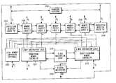
- FIG. 2is a wireless communications architecture comprising a virtual channel memory controller 210 interconnecting a digital signal processor (DSP) 212 and a reduced instruction set (RISC) processor 214 to synchronous SDRAM or SRAM 216 , and is burst FLASH/ROM 218 .
- the SDRAM/SRAMis coupled to the virtual channel memory module by a first data bus 217
- the Burst FLASH/ROM 218is coupled to the virtual channel memory controller by a second data bus 219 .
- other processor cores and synchronous memory devicesmay be used alternatively.
- the SDRAM/SRAM and Burst FLASH/ROMare coupled to the virtual channel memory controller 210 by a shared address and control bus 220 .
- the exemplary address bussupport multiplexing. A complete address is signaled to the memory device over two clock cycles; the first cycle conveys the row address and the second cycle conveys the column address.
- a first peripheral 222interfaces the DPS core with radio hardware
- a second peripheral 224interfaces the RISC core to keypads, keyboards, timers, serial communication modules, etc.
- One or more direct memory access devicefor example DMA 1 & DMA 2 devices 226 , 228 , move data from/to the memory and the peripherals via the virtual channel memory controller 210 .
- the wireless communication architecturealso includes a display controller, for example an LCD controller 230 , comprising digital logic for rendering text and/or graphical images on a display based on data stored in memory.
- a display controllerfor example an LCD controller 230 , comprising digital logic for rendering text and/or graphical images on a display based on data stored in memory.
- LCD controller 230comprising digital logic for rendering text and/or graphical images on a display based on data stored in memory.
- Other displays and corresponding controllermay be used alternatively.
- the first and second synchronous memory devicesare preferably commodity market sourced high-density memory devices, external to the virtual channel memory controller.
- the virtual channel memory controller and processor coresare disposed on a common integrated circuit 22 , and the first and second synchronous memory devices are external thereto.
- FIG. 1the virtual channel memory controller and processor cores are disposed on a common integrated circuit 22 , and the first and second synchronous memory devices are external thereto.
- the DSP and RISC cores 212 & 214 , peripherals 222 & 224 , DMA 1 and DMA 2 226 & 228 and the display controllerare integrated with the virtual channel memory controller 210 on a single application specific integrated circuit (ASIC), and the SDRAM/SRAM and FLASH/ROM memory devices are external to the ASIC.
- ASICapplication specific integrated circuit
- the preferred memory devicesare thus low cost and may be expanded without ASIC redesign.
- the shared address busreduces pin count on ASIC.
- the virtual channel memory controllersupports deep pipeline and concurrent memory access to the first and second memory devices by multiple processor cores and peripherals. In some embodiments, the virtual channel memory controller also provides memory protection as discussed more fully below.
- the first and second synchronous memory devicesare addressed with the shared address bus interconnecting the memory devices and the virtual channel memory controller.
- the first and second synchronous memory devicesare thus accessed simultaneously for memory location read/write operations by the corresponding first and second data buses. Addressing the memory devices while the memory devices are being accessed eliminates or reduces latency.
- the exemplary virtual channel memory controllercomprises a SRAM/SDRAM memory controller 320 and a Burst FLASH/ROM memory controller 322 , which are coupled to the corresponding external memory devices my corresponding data busses D 1 and D 2 as discussed above.
- the memory controllersare both coupled to the processor cores, DMAs and other controllers, for example the display controller, of FIG. 2 , by corresponding memory logic with data, address and control interfaces B 1 , B 2 , B 3 , B 4 and B 5 .
- Address bus arbitration logic 330interconnects the memory controllers 320 and 322 for resolving requests from the memory controllers for use of the shared address bus.
- the logic 330includes inputs for receiving requests from the memory controllers, and outputs for enabling memory access by the controllers. Requests are resolved on a first come, first served basis. The outputs also indicate when the address bus is busy and when the requesting controller must wait.
- a multiplexer 340routes address signals from the selected one of the first and second memory controllers 320 , 322 to the shared address bus.
- the exemplary multiplexerincludes generally a digital selector with an input s, t, from each controller, and an output “out” on the shared address bus V.
- the multiplexer outputis controlled by a “select” signal from the address bus arbitration logic 330 .
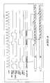
- the Row Address Strobeis signaled high for Memory Select 1 (SDRAM/SRAM) location “A”.
- the Address Bussignals “Row-A” during his time period.
- the Column Address Strobeis signaled high for Memory Select 1 (SDRAM/SRAM) location “A”.
- the Row Address Strobeis signal low, and the Address Bus signals “Col-A”.
- Clock times 4 - 7no memory locations are addressed.
- the address busdoes not change state from is last state, “Col-B”, thus reducing power consumption associated with signal transitions on the address bus.
- Clock time 4 - 7the data busses D 1 and D 2 are idle since there were no prior data requests in the example. If the memory access is a read, the memories are retrieving data requested during this time, the memory latency period.
- the first data word of a burst of 8 data words from SDRAM/SRAMappears on the data bus D 1 .
- the Row Address Strobeis signaled high for Memory Select 1 (SDRAM/SRAM) location “C”, and the Address Bus signals “Row-C”.
- the Column Address Strobeis signaled high for Memory Select 1 (SDRAM/SRAM) location “C”.
- the Row Address Strobeis signal low, and the Address Bus signals “Col-C”.
- the address busis inactive, and the first data word of the 8 bit data word burst from FLASH/ROM appears on data bus D 2 .
- the Row Address Strobeis signaled high for Memory Select 2 (FLASH/ROM) location “D”, and the Address Bus signals “Row-D” during concurrent access to the SDRAM/SRAM and FLASH ROM memories.
- the exemplary virtual channel memory controlleralso comprises a group of shared memory space access registers, or Semaphore registers 350 , interconnecting the first and second processor core memory access register blocks 352 , 354 .
- the first and second memory access register blocks 352 , 354are coupled to corresponding processor logic blocks 356 , 358 for conveying address ranges and restrictions for the core processors.
- the semaphore registers 350convey access permission to the shared memory space.
- the Semaphore register settingsonly indicate memory access policy.
- the shared memory spacefacilitates interprocessor communication of data and other information by passing by reference, rather than copying data from one memory to the other.
- the first and second processor core memory access register blocks 356 and 358define memory access permission and enforce protected memory areas on the processor cores. Thus configured, the processor cores cannot change the memory access configuration for other processor core.
- the exemplary virtual channel memory controllerincludes an optional local on-chip memory controller 360 for controlling local RAM/ROM illustrated in FIG. 2 .
- the on-chip memory controller 360has relatively low access times and thus does not require the deep pipelining and latency-hiding scheme discussed above in connection with the first and second external memory devices.
Landscapes
- Engineering & Computer Science (AREA)
- Theoretical Computer Science (AREA)
- Physics & Mathematics (AREA)
- General Engineering & Computer Science (AREA)
- General Physics & Mathematics (AREA)
- Multi Processors (AREA)
- Memory System (AREA)
Abstract
Description
Claims (40)
Priority Applications (2)
| Application Number | Priority Date | Filing Date | Title |
|---|---|---|---|
| US10/008,939US6950910B2 (en) | 2001-11-08 | 2001-11-08 | Mobile wireless communication device architectures and methods therefor |
| US11/220,735US7127563B2 (en) | 2001-11-08 | 2005-09-07 | Shared memory architecture |
Applications Claiming Priority (1)
| Application Number | Priority Date | Filing Date | Title |
|---|---|---|---|
| US10/008,939US6950910B2 (en) | 2001-11-08 | 2001-11-08 | Mobile wireless communication device architectures and methods therefor |
Related Child Applications (1)
| Application Number | Title | Priority Date | Filing Date |
|---|---|---|---|
| US11/220,735ContinuationUS7127563B2 (en) | 2001-11-08 | 2005-09-07 | Shared memory architecture |
Publications (2)
| Publication Number | Publication Date |
|---|---|
| US20030088743A1 US20030088743A1 (en) | 2003-05-08 |
| US6950910B2true US6950910B2 (en) | 2005-09-27 |
Family
ID=21734594
Family Applications (2)
| Application Number | Title | Priority Date | Filing Date |
|---|---|---|---|
| US10/008,939Expired - LifetimeUS6950910B2 (en) | 2001-11-08 | 2001-11-08 | Mobile wireless communication device architectures and methods therefor |
| US11/220,735Expired - LifetimeUS7127563B2 (en) | 2001-11-08 | 2005-09-07 | Shared memory architecture |
Family Applications After (1)
| Application Number | Title | Priority Date | Filing Date |
|---|---|---|---|
| US11/220,735Expired - LifetimeUS7127563B2 (en) | 2001-11-08 | 2005-09-07 | Shared memory architecture |
Country Status (1)
| Country | Link |
|---|---|
| US (2) | US6950910B2 (en) |
Cited By (2)
| Publication number | Priority date | Publication date | Assignee | Title |
|---|---|---|---|---|
| US20040204080A1 (en)* | 2002-12-09 | 2004-10-14 | Hayduk Matthew A. | Audio over subsystem interface |
| US20070024436A1 (en)* | 2005-07-28 | 2007-02-01 | Symbol Technologies, Inc. | Method and apparatus for a product information interface utilizing radio frequency identification (RFID) technology |
Families Citing this family (46)
| Publication number | Priority date | Publication date | Assignee | Title |
|---|---|---|---|---|
| US7100071B2 (en)* | 1998-07-16 | 2006-08-29 | Hewlett-Packard Development Company, L.P. | System and method for allocating fail-over memory |
| US7280428B2 (en) | 2004-09-30 | 2007-10-09 | Rambus Inc. | Multi-column addressing mode memory system including an integrated circuit memory device |
| US8595459B2 (en) | 2004-11-29 | 2013-11-26 | Rambus Inc. | Micro-threaded memory |
| US8335894B1 (en) | 2008-07-25 | 2012-12-18 | Google Inc. | Configurable memory system with interface circuit |
| US8796830B1 (en) | 2006-09-01 | 2014-08-05 | Google Inc. | Stackable low-profile lead frame package |
| US7609567B2 (en)* | 2005-06-24 | 2009-10-27 | Metaram, Inc. | System and method for simulating an aspect of a memory circuit |
| US8055833B2 (en) | 2006-10-05 | 2011-11-08 | Google Inc. | System and method for increasing capacity, performance, and flexibility of flash storage |
| US8386722B1 (en) | 2008-06-23 | 2013-02-26 | Google Inc. | Stacked DIMM memory interface |
| US9171585B2 (en) | 2005-06-24 | 2015-10-27 | Google Inc. | Configurable memory circuit system and method |
| US10013371B2 (en) | 2005-06-24 | 2018-07-03 | Google Llc | Configurable memory circuit system and method |
| US8111566B1 (en) | 2007-11-16 | 2012-02-07 | Google, Inc. | Optimal channel design for memory devices for providing a high-speed memory interface |
| US9507739B2 (en) | 2005-06-24 | 2016-11-29 | Google Inc. | Configurable memory circuit system and method |
| US8060774B2 (en) | 2005-06-24 | 2011-11-15 | Google Inc. | Memory systems and memory modules |
| US8041881B2 (en) | 2006-07-31 | 2011-10-18 | Google Inc. | Memory device with emulated characteristics |
| US8077535B2 (en) | 2006-07-31 | 2011-12-13 | Google Inc. | Memory refresh apparatus and method |
| US8359187B2 (en) | 2005-06-24 | 2013-01-22 | Google Inc. | Simulating a different number of memory circuit devices |
| US8438328B2 (en)* | 2008-02-21 | 2013-05-07 | Google Inc. | Emulation of abstracted DIMMs using abstracted DRAMs |
| US8130560B1 (en) | 2006-11-13 | 2012-03-06 | Google Inc. | Multi-rank partial width memory modules |
| US8327104B2 (en) | 2006-07-31 | 2012-12-04 | Google Inc. | Adjusting the timing of signals associated with a memory system |
| US20080028136A1 (en)* | 2006-07-31 | 2008-01-31 | Schakel Keith R | Method and apparatus for refresh management of memory modules |
| US8081474B1 (en) | 2007-12-18 | 2011-12-20 | Google Inc. | Embossed heat spreader |
| US7386656B2 (en) | 2006-07-31 | 2008-06-10 | Metaram, Inc. | Interface circuit system and method for performing power management operations in conjunction with only a portion of a memory circuit |
| US20080082763A1 (en) | 2006-10-02 | 2008-04-03 | Metaram, Inc. | Apparatus and method for power management of memory circuits by a system or component thereof |
| US8244971B2 (en) | 2006-07-31 | 2012-08-14 | Google Inc. | Memory circuit system and method |
| US8089795B2 (en) | 2006-02-09 | 2012-01-03 | Google Inc. | Memory module with memory stack and interface with enhanced capabilities |
| US8397013B1 (en) | 2006-10-05 | 2013-03-12 | Google Inc. | Hybrid memory module |
| US9542352B2 (en) | 2006-02-09 | 2017-01-10 | Google Inc. | System and method for reducing command scheduling constraints of memory circuits |
| US7543126B2 (en)* | 2005-08-31 | 2009-06-02 | International Business Machines Corporation | Apparatus, system, and method for implementing protected virtual memory subcontexts |
| WO2007028109A2 (en) | 2005-09-02 | 2007-03-08 | Metaram, Inc. | Methods and apparatus of stacking drams |
| KR100745369B1 (en)* | 2005-12-22 | 2007-08-02 | 삼성전자주식회사 | Multipath Accessible Semiconductor Memory Device with Port State Signaling |
| US9632929B2 (en) | 2006-02-09 | 2017-04-25 | Google Inc. | Translating an address associated with a command communicated between a system and memory circuits |
| EP2696290B1 (en)* | 2006-02-09 | 2015-12-23 | Google, Inc. | Memory circuit system and method |
| US20070260841A1 (en) | 2006-05-02 | 2007-11-08 | Hampel Craig E | Memory module with reduced access granularity |
| US7769942B2 (en) | 2006-07-27 | 2010-08-03 | Rambus, Inc. | Cross-threaded memory system |
| US20110016278A1 (en)* | 2008-03-31 | 2011-01-20 | Frederick Ware | Independent Threading of Memory Devices Disposed on Memory Modules |
| US8621159B2 (en) | 2009-02-11 | 2013-12-31 | Rambus Inc. | Shared access memory scheme |
| DE202010017690U1 (en) | 2009-06-09 | 2012-05-29 | Google, Inc. | Programming dimming terminating resistor values |
| US8914568B2 (en)* | 2009-12-23 | 2014-12-16 | Intel Corporation | Hybrid memory architectures |
| EP2539823B1 (en) | 2010-02-23 | 2016-04-13 | Rambus Inc. | Time multiplexing at different rates to access different memory types |
| US9268719B2 (en) | 2011-08-05 | 2016-02-23 | Rambus Inc. | Memory signal buffers and modules supporting variable access granularity |
| CN103019620A (en)* | 2012-11-30 | 2013-04-03 | 中国科学院上海技术物理研究所 | Storage circuit system based on flash memory-SRAM (Static Random Access Memory) flow line |
| KR102181441B1 (en) | 2014-04-15 | 2020-11-24 | 에스케이하이닉스 주식회사 | Semiconductor device including plurality of function blocks |
| US9990131B2 (en)* | 2014-09-22 | 2018-06-05 | Xilinx, Inc. | Managing memory in a multiprocessor system |
| EP3201342A4 (en) | 2014-10-01 | 2018-07-25 | National Research Council of Canada | Animal models, cell lines and methods for screening hepatitis c virus vaccines |
| US10579563B2 (en)* | 2017-06-16 | 2020-03-03 | Honeywell International Inc. | Multiple master process controllers using a shared serial peripheral bus |
| CN115658560B (en)* | 2022-12-28 | 2023-03-14 | 北京紫光芯能科技有限公司 | Data sharing management method, device and system, electronic equipment and storage medium |
Citations (6)
| Publication number | Priority date | Publication date | Assignee | Title |
|---|---|---|---|---|
| US5978866A (en)* | 1997-03-10 | 1999-11-02 | Integrated Technology Express, Inc. | Distributed pre-fetch buffer for multiple DMA channel device |
| US6021077A (en)* | 1996-07-22 | 2000-02-01 | Nec Corporation | Semiconductor memory device controlled in synchronous with external clock |
| US20010053069A1 (en)* | 2000-05-10 | 2001-12-20 | Rambus Inc. | Multiple channel modules and bus systems using same |
| US20020174311A1 (en)* | 2001-04-24 | 2002-11-21 | Ware Frederick A. | Method and apparatus for coordinating memory operations among diversely-located memory components |
| US20030105906A1 (en)* | 2001-11-15 | 2003-06-05 | Nokia Corporation | Data processor architecture employing segregated data, program and control buses |
| US6611537B1 (en)* | 1997-05-30 | 2003-08-26 | Centillium Communications, Inc. | Synchronous network for digital media streams |
- 2001
- 2001-11-08USUS10/008,939patent/US6950910B2/ennot_activeExpired - Lifetime
- 2005
- 2005-09-07USUS11/220,735patent/US7127563B2/ennot_activeExpired - Lifetime
Patent Citations (6)
| Publication number | Priority date | Publication date | Assignee | Title |
|---|---|---|---|---|
| US6021077A (en)* | 1996-07-22 | 2000-02-01 | Nec Corporation | Semiconductor memory device controlled in synchronous with external clock |
| US5978866A (en)* | 1997-03-10 | 1999-11-02 | Integrated Technology Express, Inc. | Distributed pre-fetch buffer for multiple DMA channel device |
| US6611537B1 (en)* | 1997-05-30 | 2003-08-26 | Centillium Communications, Inc. | Synchronous network for digital media streams |
| US20010053069A1 (en)* | 2000-05-10 | 2001-12-20 | Rambus Inc. | Multiple channel modules and bus systems using same |
| US20020174311A1 (en)* | 2001-04-24 | 2002-11-21 | Ware Frederick A. | Method and apparatus for coordinating memory operations among diversely-located memory components |
| US20030105906A1 (en)* | 2001-11-15 | 2003-06-05 | Nokia Corporation | Data processor architecture employing segregated data, program and control buses |
Cited By (3)
| Publication number | Priority date | Publication date | Assignee | Title |
|---|---|---|---|---|
| US20040204080A1 (en)* | 2002-12-09 | 2004-10-14 | Hayduk Matthew A. | Audio over subsystem interface |
| US7596384B2 (en)* | 2002-12-09 | 2009-09-29 | Intel Corporation | Audio over subsystem interface |
| US20070024436A1 (en)* | 2005-07-28 | 2007-02-01 | Symbol Technologies, Inc. | Method and apparatus for a product information interface utilizing radio frequency identification (RFID) technology |
Also Published As
| Publication number | Publication date |
|---|---|
| US7127563B2 (en) | 2006-10-24 |
| US20030088743A1 (en) | 2003-05-08 |
| US20060004976A1 (en) | 2006-01-05 |
Similar Documents
| Publication | Publication Date | Title |
|---|---|---|
| US6950910B2 (en) | Mobile wireless communication device architectures and methods therefor | |
| US6532525B1 (en) | Method and apparatus for accessing memory | |
| US7380045B2 (en) | Protocol conversion and arbitration circuit, system having the same, and method for converting and arbitrating signals | |
| CN101036131B (en) | Error-correcting coded memory transaction burst operations and memory components supporting temporal multiplexing | |
| US6954821B2 (en) | Crossbar switch that supports a multi-port slave device and method of operation | |
| EP1239374B1 (en) | Shared program memory for use in multicore DSP devices | |
| US7793008B2 (en) | AMBA modular memory controller | |
| US6425044B1 (en) | Apparatus for providing fast memory decode using a bank conflict table | |
| CN100499556C (en) | High-speed asynchronous interlinkage communication network of heterogeneous multi-nucleus processor | |
| KR100814904B1 (en) | On-Chip Communication architecture | |
| US7725621B2 (en) | Semiconductor device and data transfer method | |
| US8713233B2 (en) | Interconnect, bus system with interconnect and bus system operating method | |
| US20070136503A1 (en) | Systems for implementing SDRAM controllers, and buses adapted to include advanced high performance bus features | |
| JP2002049576A (en) | Bus architecture for system mounted on chip | |
| CN100419901C (en) | Memory device with different burst sequential addressing for read and write operations | |
| US7916720B2 (en) | Slave network interface circuit for improving parallelism of on-chip network and system thereof | |
| US6502173B1 (en) | System for accessing memory and method therefore | |
| US20070156937A1 (en) | Data transfer in multiprocessor system | |
| US10346328B2 (en) | Method and apparatus for indicating interrupts | |
| CN110633230A (en) | High bandwidth DIMM | |
| US20150177816A1 (en) | Semiconductor integrated circuit apparatus | |
| EP1588276B1 (en) | Processor array | |
| JP6294732B2 (en) | Data transfer control device and memory built-in device | |
| US7069363B1 (en) | On-chip bus | |
| US7185133B2 (en) | Data processor |
Legal Events
| Date | Code | Title | Description |
|---|---|---|---|
| AS | Assignment | Owner name:MOTOROLA, INC., ILLINOIS Free format text:ASSIGNMENT OF ASSIGNORS INTEREST;ASSIGNOR:RADER, SHEILA M.;REEL/FRAME:012370/0951 Effective date:20011107 | |
| AS | Assignment | Owner name:FREESCALE SEMICONDUCTOR, INC., TEXAS Free format text:ASSIGNMENT OF ASSIGNORS INTEREST;ASSIGNOR:MOTOROLA, INC;REEL/FRAME:015360/0718 Effective date:20040404 Owner name:FREESCALE SEMICONDUCTOR, INC.,TEXAS Free format text:ASSIGNMENT OF ASSIGNORS INTEREST;ASSIGNOR:MOTOROLA, INC;REEL/FRAME:015360/0718 Effective date:20040404 | |
| STCF | Information on status: patent grant | Free format text:PATENTED CASE | |
| AS | Assignment | Owner name:CITIBANK, N.A. AS COLLATERAL AGENT, NEW YORK Free format text:SECURITY AGREEMENT;ASSIGNORS:FREESCALE SEMICONDUCTOR, INC.;FREESCALE ACQUISITION CORPORATION;FREESCALE ACQUISITION HOLDINGS CORP.;AND OTHERS;REEL/FRAME:018855/0129 Effective date:20061201 Owner name:CITIBANK, N.A. AS COLLATERAL AGENT,NEW YORK Free format text:SECURITY AGREEMENT;ASSIGNORS:FREESCALE SEMICONDUCTOR, INC.;FREESCALE ACQUISITION CORPORATION;FREESCALE ACQUISITION HOLDINGS CORP.;AND OTHERS;REEL/FRAME:018855/0129 Effective date:20061201 | |
| CC | Certificate of correction | ||
| FPAY | Fee payment | Year of fee payment:4 | |
| AS | Assignment | Owner name:CITIBANK, N.A., AS COLLATERAL AGENT,NEW YORK Free format text:SECURITY AGREEMENT;ASSIGNOR:FREESCALE SEMICONDUCTOR, INC.;REEL/FRAME:024397/0001 Effective date:20100413 Owner name:CITIBANK, N.A., AS COLLATERAL AGENT, NEW YORK Free format text:SECURITY AGREEMENT;ASSIGNOR:FREESCALE SEMICONDUCTOR, INC.;REEL/FRAME:024397/0001 Effective date:20100413 | |
| AS | Assignment | Owner name:APPLE INC., CALIFORNIA Free format text:ASSIGNMENT OF ASSIGNORS INTEREST;ASSIGNOR:FREESCALE SEMICONDUCTOR, INC.;REEL/FRAME:026304/0200 Effective date:20110411 | |
| FPAY | Fee payment | Year of fee payment:8 | |
| AS | Assignment | Owner name:FREESCALE SEMICONDUCTOR, INC., TEXAS Free format text:PATENT RELEASE;ASSIGNOR:CITIBANK, N.A., AS COLLATERAL AGENT;REEL/FRAME:037354/0225 Effective date:20151207 Owner name:FREESCALE SEMICONDUCTOR, INC., TEXAS Free format text:PATENT RELEASE;ASSIGNOR:CITIBANK, N.A., AS COLLATERAL AGENT;REEL/FRAME:037356/0143 Effective date:20151207 Owner name:FREESCALE SEMICONDUCTOR, INC., TEXAS Free format text:PATENT RELEASE;ASSIGNOR:CITIBANK, N.A., AS COLLATERAL AGENT;REEL/FRAME:037356/0553 Effective date:20151207 | |
| FPAY | Fee payment | Year of fee payment:12 |