US6950321B2 - Active damping control for L-C output filters in three phase four-leg inverters - Google Patents
Active damping control for L-C output filters in three phase four-leg invertersDownload PDFInfo
- Publication number
- US6950321B2 US6950321B2US10/669,618US66961803AUS6950321B2US 6950321 B2US6950321 B2US 6950321B2US 66961803 AUS66961803 AUS 66961803AUS 6950321 B2US6950321 B2US 6950321B2
- Authority
- US
- United States
- Prior art keywords
- axis
- zero
- inverter
- filter
- voltage
- Prior art date
- Legal status (The legal status is an assumption and is not a legal conclusion. Google has not performed a legal analysis and makes no representation as to the accuracy of the status listed.)
- Expired - Lifetime, expires
Links
- 238000013016dampingMethods0.000titleclaimsabstractdescription46
- 230000001105regulatory effectEffects0.000claimsabstractdescription47
- 238000000034methodMethods0.000claimsabstractdescription25
- 230000033228biological regulationEffects0.000claimsabstractdescription17
- 230000001276controlling effectEffects0.000claimsabstractdescription4
- 238000012937correctionMethods0.000claimsdescription32
- 230000009466transformationEffects0.000claimsdescription15
- 230000008569processEffects0.000claimsdescription12
- 230000001131transforming effectEffects0.000claimsdescription6
- 230000001934delayEffects0.000claimsdescription4
- 238000005070samplingMethods0.000claimsdescription2
- 230000000694effectsEffects0.000claims1
- 230000010355oscillationEffects0.000description8
- 230000007935neutral effectEffects0.000description7
- 238000010586diagramMethods0.000description6
- 239000003990capacitorSubstances0.000description4
- 230000001052transient effectEffects0.000description4
- 238000013459approachMethods0.000description3
- 230000004044responseEffects0.000description3
- 230000001360synchronised effectEffects0.000description3
- 239000002131composite materialSubstances0.000description2
- 230000000593degrading effectEffects0.000description2
- 230000002411adverseEffects0.000description1
- 230000008901benefitEffects0.000description1
- 230000015556catabolic processEffects0.000description1
- 238000007796conventional methodMethods0.000description1
- 230000008878couplingEffects0.000description1
- 238000010168coupling processMethods0.000description1
- 238000005859coupling reactionMethods0.000description1
- 238000006731degradation reactionMethods0.000description1
- 239000000446fuelSubstances0.000description1
- 238000009499grossingMethods0.000description1
- 238000002372labellingMethods0.000description1
- 230000000116mitigating effectEffects0.000description1
- 238000010248power generationMethods0.000description1
- 230000006641stabilisationEffects0.000description1
- 238000011105stabilizationMethods0.000description1
- 230000001629suppressionEffects0.000description1
- 238000012360testing methodMethods0.000description1
- 238000000844transformationMethods0.000description1
- 238000012795verificationMethods0.000description1
Images


Classifications
- H—ELECTRICITY
- H02—GENERATION; CONVERSION OR DISTRIBUTION OF ELECTRIC POWER
- H02M—APPARATUS FOR CONVERSION BETWEEN AC AND AC, BETWEEN AC AND DC, OR BETWEEN DC AND DC, AND FOR USE WITH MAINS OR SIMILAR POWER SUPPLY SYSTEMS; CONVERSION OF DC OR AC INPUT POWER INTO SURGE OUTPUT POWER; CONTROL OR REGULATION THEREOF
- H02M7/00—Conversion of AC power input into DC power output; Conversion of DC power input into AC power output
- H02M7/42—Conversion of DC power input into AC power output without possibility of reversal
- H02M7/44—Conversion of DC power input into AC power output without possibility of reversal by static converters
- H02M7/48—Conversion of DC power input into AC power output without possibility of reversal by static converters using discharge tubes with control electrode or semiconductor devices with control electrode
- H02M7/53—Conversion of DC power input into AC power output without possibility of reversal by static converters using discharge tubes with control electrode or semiconductor devices with control electrode using devices of a triode or transistor type requiring continuous application of a control signal
- H02M7/537—Conversion of DC power input into AC power output without possibility of reversal by static converters using discharge tubes with control electrode or semiconductor devices with control electrode using devices of a triode or transistor type requiring continuous application of a control signal using semiconductor devices only, e.g. single switched pulse inverters
- H02M7/5387—Conversion of DC power input into AC power output without possibility of reversal by static converters using discharge tubes with control electrode or semiconductor devices with control electrode using devices of a triode or transistor type requiring continuous application of a control signal using semiconductor devices only, e.g. single switched pulse inverters in a bridge configuration
- H02M7/53871—Conversion of DC power input into AC power output without possibility of reversal by static converters using discharge tubes with control electrode or semiconductor devices with control electrode using devices of a triode or transistor type requiring continuous application of a control signal using semiconductor devices only, e.g. single switched pulse inverters in a bridge configuration with automatic control of output voltage or current
- H02M7/53875—Conversion of DC power input into AC power output without possibility of reversal by static converters using discharge tubes with control electrode or semiconductor devices with control electrode using devices of a triode or transistor type requiring continuous application of a control signal using semiconductor devices only, e.g. single switched pulse inverters in a bridge configuration with automatic control of output voltage or current with analogue control of three-phase output
- H—ELECTRICITY
- H02—GENERATION; CONVERSION OR DISTRIBUTION OF ELECTRIC POWER
- H02M—APPARATUS FOR CONVERSION BETWEEN AC AND AC, BETWEEN AC AND DC, OR BETWEEN DC AND DC, AND FOR USE WITH MAINS OR SIMILAR POWER SUPPLY SYSTEMS; CONVERSION OF DC OR AC INPUT POWER INTO SURGE OUTPUT POWER; CONTROL OR REGULATION THEREOF
- H02M1/00—Details of apparatus for conversion
- H02M1/12—Arrangements for reducing harmonics from AC input or output
- H02M1/123—Suppression of common mode voltage or current
Definitions
- the present inventiongenerally relates to three-phase voltage source inverters, and more particularly relates to the damping control of the L-C output filters in three-phase four-leg voltage source inverters.
- Three-phase voltage source invertersare generally used to convert DC power into three-phase AC power.
- the three-phase output voltagesare sinusoidal waveforms spaced 120 degrees apart, to be compatible with a wide variety of applications requiring conventional AC power.
- the output power frequencies commonly usedare 50, 60, and 400 hertz, but other frequencies could be used as well.
- a DC power sourcesuch as a battery, fuel cell array, or other equivalent device, is converted into an AC power supply for various internal control functions, including the propulsion system.
- the quality of an inverteris generally determined by its output voltage and frequency stability, and by the total harmonic distortion of its output waveforms.
- a high quality invertershould maintain its output stability in the presence of load current variations and load imbalances.
- the 4-leg three-phase inverter topologyis generally considered to offer superior performance than a 3-leg three-phase topology. That is, with an unbalanced load, the 3-phase output currents from an inverter will generally not add up to zero, as they would in a 3-leg balanced load situation. Therefore, a fourth (neutral) leg is typically added to accommodate the imbalance in current flow caused by an unbalanced load. If a neutral is not used with an unbalanced load, voltage imbalances may occur at the load terminals, and the output power quality may be adversely affected.
- the operational functions of a typical inverterare generally controlled by drive signals from an automatic controller.
- the controller and inverterare usually implemented as a closed loop control system, with the inverter output being sampled to provide regulating feedback signals to the controller.
- the feedback signalstypically include samples of the output voltage and current signals, and can also include harmonics of the fundamental output frequency.
- L-C filter3-phase inductor-capacitor (L-C) filter, which is normally connected at the output of the inverter.
- L-C filterhas very low component resistance, and may exhibit under-damped behavior. This behavior can lead to filter oscillations as a result of sudden changes in the inverter load, and can create distortion or over-voltages on the load.
- the typical voltage control loop response of an inverter controllermay be inadequate to compensate for this type of L-C filter oscillation.
- an inverter controllerwith a damping control scheme that will reduce the tendency of the L-C output filter to oscillate without degrading the efficiency of the inverter.
- an inverter controllerwith a damping scheme that will also improve the transient performance of the inverter.
- methods and devicesare provided for controlling a multi-phase inverter having an under-damped L-C filter connected to a load.
- the inverter outputis sampled to generate feedback voltage and current signals. These signals are processed to generate voltage regulation signals and damping signals.
- the voltage regulation signalscomprise regulating and imbalance compensating elements, and are further modified by damping signals.
- the modified voltage regulation signalsare processed into control signals for the inverter to stabilize the inverter output to the load.
- An exemplary embodiment of a devicefor controlling a multi-phase inverter having an under-damped L-C filter connected to a load.
- the deviceincludes means for sampling the multi-phase inverter output and for generating damping correction signals.
- the multi-phase outputis also processed through a converter, which transforms the multi-phase output into d-axis, q-axis and zero-axis voltage and current elements. These elements are processed in corresponding regulators to generate voltage regulation signals, each of which comprises a compensating fundamental component and a compensating imbalance component.
- the zero-axis voltage regulation signalis modified by an active damping filter, and the d-axis, q-axis and zero-axis voltage regulation signals are combined with the corresponding damping correction signals in a drive controller.
- the drive controllerprocesses the corrected voltage regulating signals into control inputs for the inverter switching circuits, which enable the inverter to damp the L-C filter and to regulate the fundamental and imbalance characteristics of the multi-phase output.
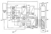
- FIG. 1is a block diagram of an exemplary four-leg three-phase inverter system
- FIG. 2is a simplified block diagram of an exemplary inverter controller with active damping
- FIG. 3is a detailed block diagram of an exemplary embodiment of an inverter controller with active damping
- FIG. 4is a block diagram of an exemplary embodiment of an active damping scheme.
- Various embodiments of the present inventionpertain to the area of voltage source inverters operating in a stand-alone mode.
- this type of inverteris used to convert DC power available at a selected voltage into AC power with fixed voltage and frequency.
- the output voltage and frequency stability of an invertershould be independent of load variations and imbalances.
- an inverter controllermay be used in a closed loop feedback configuration to provide regulating and imbalance compensating signals to the inverter.
- the inverter controllermay be implemented in hardware or software, or any combination of the two.
- the four-leg inverter topologyis generally used for quality AC power generation into a three-phase unbalanced load application.
- the fourth legprovides a return path for the neutral imbalance current of a three-phase load.
- a three-leg inverter configurationtypically connects the load neutral to the mid-point of two series-connected capacitors across the DC voltage source.
- the AC output voltagewould be approximately 0.5 Vdc
- the four-leg configurationprovides an AC output voltage of approximately 0.578 Vdc.
- a further advantage of the four-leg configurationis that a smaller, single capacitor can be used instead of the two required for the three-leg approach.
- a DC voltage source 102supplies a selected level of voltage (Vdc) to an inverter/filter 104 connected to a three-phase four-wire load 106 .
- Inverter/filter 104typically comprises an input (link) capacitor C L connected across source 102 , and in parallel with four sets of switching circuits 103 , which generate a three-phase output signal via L-C filter 105 to the load 106 .
- Inductor L nrepresents the inductance of the neutral line.
- An inverter controller 108is typically configured to receive voltage and frequency command signals from a control unit (not shown in FIG. 1 ), and to also receive feedback signals from the input Vdc and from the outputs of inverter/filter 104 at the inputs to load 106 . Inverter controller 108 processes the command and feedback signals to create output drive signals for the inverter/filter 104 switching circuits 103 .
- the inverter controller 108 output drive signalstypically include voltage and current regulating elements, and may also include load imbalance and filter under-damping compensation elements.
- FIG. 2depicts a simplified block diagram of inverter controller 108 within the closed loop four-leg three-phase inverter system 100 .
- an external control unit 110typically provides reference signals, such as voltage, current, frequency, etc., to inverter controller 108 to establish the desired output voltage and frequency values of inverter/filter 104 .
- control unit 110could be integrated within inverter controller 108 .
- Voltage regulator blocks 112 , 114 , 116receive voltage reference signals from control unit 110 while a current limiting block 126 receives a current reference signal from control unit 110 .
- Samples of the voltage and current outputs from L-C filter 105are transformed from the AC domain to the DC domain in block 124 , which receives a frequency reference signal from control unit 110 .
- Voltage feedback signals from block 124are fed to corresponding voltage regulator blocks 112 , 114 , 116 , and current feedback signals from block 124 are fed to current limiting block 126 .
- a current limiting signal from block 126is applied to voltage regulator blocks 112 , 114 , 116 .
- Voltage regulating blocks 112 , 114 , 116generate regulating signal outputs that are limited by the output of current limiting block 126 .
- the regulating signal outputsare inverse transformed from the DC domain to the AC domain in block 120 , which receives a frequency reference signal from control unit 110 .
- the transformed regulating signalsare then processed by block 122 into driving signals for the inverter 104 switching circuits 103 .
- samples of the voltage outputs from L-C filter 105are also connected to an active damping filter 130 , which processes the voltage samples into voltage correction signals.
- the voltage correction signalsare used as a damping influence on the driving signals generated by block 122 .
- active damping filter 130provides a damping factor to voltage regulator block 116 .
- inverter controller 108A more detailed description of the operation of inverter controller 108 is given below in conjunction with FIG. 3 .
- FIG. 3An exemplary embodiment of an inverter controller 108 for a four-leg three-phase inverter/filter 104 is shown in a more detailed block diagram form in FIG. 3 .
- the block functions within inverter controller 108are implemented in software modules to constitute a control algorithm for inverter/filter 104 .
- This approachutilizes the Park transformation, as is known in the electrical machine art (see “Analysis of Electric Machinery” by Krause, Paul C., Wasynczuk, Oleg and Sudhoff, Scott D.; IEEE Press, 1995, Institute of Electrical and Electronics Engineers, Inc.), to convert the sampled output signals from an AC domain to a DC domain in order to simplify the mathematical processes implemented within inverter controller 108 .
- An inverse Park transformationis then used to convert the processed DC domain signals back to the AC domain for the control inputs to the inverter switching circuits 103 .
- Other techniques for converting from the AC domain to the DC domaincould be used in a wide array of equivalent embodiments.
- the basic concept of the Park transformationis known as the synchronous reference frame approach. That is, a rotating reference frame is utilized in order to make the fundamental frequency quantities appear as DC values.
- a common conventionis to label the AC domain (stationary reference frame) quantities, such as phase voltages and currents, as “abc”, and to label the corresponding Park-transformed DC domain (synchronous reference frame) quantities as “dq 0 ”. This labeling convention will be followed throughout the following discussion.
- controller 108is configured to process regulating signals that control the input signals to the switching circuits 103 of inverter 104 .
- These regulating signalsare typically derived from reference signals and feedback signals, and can be processed in controller 108 to provide composite voltage regulating and imbalance compensation signals to drive switching circuits 103 .
- the disclosed exemplary embodimentalso provides active damping for L-C filter 105 , in conjunction with the composite voltage regulating and imbalance compensation signals.
- inverter L-C filtersmay be susceptible to oscillation under certain types of load transients.
- the cut-off frequencyis usually in excess of 1 kHz, in order to minimize the size and weight of the filter components.
- an under-damped L-C filter oscillation at this frequencywould usually be out of the regulation bandwidth of an inverter controller, and would probably not be eliminated through typical regulating actions.
- the exemplary embodimentincludes an active damping control to reduce the oscillation susceptibility of an L-C filter.
- reference values for voltage, current and frequencyare generally determined within a control unit 110 to establish desired values of inverter output voltage and frequency within a maximum current limit.
- the voltage referencesare V* d , V* q , V* 0 , which are typically calculated Park transformations of predetermined reference three-phase voltage values.
- the maximum current limit valueis shown in FIG. 3 as I inv — max , and the reference frequency is represented as ⁇ *.
- the inverter/filter 104 three-phase output voltages and currentsmay be measured by any conventional method to create feedback signals to inverter controller 108 .
- the voltage feedback signalsare typically measured between phase and neutral, and are designated herein as V a n, V bn , V cn .
- the current feedback signalscan be measured by line sensors on each phase, and are designated herein as I a , I b , I c .
- Voltage feedback signals V an , V bn , V cnare inputted in parallel to transform block 124 and to active damping block 130 .
- active damping block 130The operation of active damping block 130 will be described in a later section of this Detailed Description.
- Voltage feedback signals V an , V bn , V cnare converted from AC domain to DC domain equivalents via the Park transformation in block 124 .
- the reference angle used for this transformationis designated ⁇ *, and is generated by an integrator block 23 from the reference signal ⁇ *.
- the transformed voltage feedback signalsare designated V d , V q , V 0 and are fed back to adders 1120 , 1140 and 1160 , respectively.
- the reference voltage signals V* d , V* q , V* 0are also inputted to adders 1120 , 1140 and 1160 , respectively, to generate voltage error signals (V* d -V d , V* q -V q , V* 0 -V 0 ) at the outputs of the respective adders 1120 , 1140 , 1160 .
- the voltage error signals V* d -V d , V* q -V q , V* 0 -V 0are routed through proportional-integral (PI) controller blocks 1122 , 1142 , and 1162 , respectively, for amplifying and smoothing.
- voltage error signals V* d -V d , V* q -V q , V* 0 -V 0are also routed through band pass filter blocks 1128 , 1148 , and 1168 , respectively.
- block 1128is configured as a second order band pass filter with an adjustable gain.
- the center frequency of filter 1128is set at twice the reference frequency ⁇ *, in order to provide a high gain for the d-axis voltage controller at this particular frequency. This is intended to compensate for an unbalanced inverter output voltage condition, where a voltage component at twice the fundamental frequency appears in the voltage feedback signal.
- band pass filter 1128By placing band pass filter 1128 in a parallel path within the d-axis voltage controller 112 , the loop gain can be increased at 2* ⁇ * without affecting the phase and gain margin of the system.
- the output signals from blocks 1122 and 1128are combined in adder 1124 , along with a quantity ⁇ *LI q .
- This latter quantityis a feed-forward term, which may be obtained from control unit 110 by transforming the steady-state equations of the filter 105 from the stationary reference frame to the synchronous reference frame.
- the feed-forward term ⁇ *L qis used in this embodiment to improve the transient response of the d-axis voltage regulator 112 , and to reduce the cross-channel coupling between the d-axis and q-axis controllers ( 112 and 114 ).
- the corresponding feed-forward termis ⁇ *LI d .
- the q-axis voltage regulator 114operates in essentially the same manner as the d-axis voltage regulator 112 , except for the feed-forward term, as noted above.
- the 0-axis voltage regulator 116differs from the d-axis and q-axis regulators ( 112 , 114 ) in that its associated band pass filter 1168 is tuned to ⁇ *, rather than 2* ⁇ *. This is due to the fact that an unbalanced output voltage condition will generally produce a fundamental frequency component on the 0-axis feedback signal. Also, there is generally no need for a feed-forward signal in the 0-axis channel.
- Active damping block 130also plays a role in the operation of 0-axis voltage regulator 116 , as shown in FIGS. 3 and 4 .
- the error voltage (V* 0 -V 0 ) generated at the output of adder 1160is fed back to one channel of block 130 , and is designated as the zero-sequence voltage error in FIG. 4 .
- the zero-sequence voltage erroris routed through a band pass filter 132 , which is tuned to half the L-C output filter frequency ( ⁇ f /2).
- the equivalent inductance in the 0-axis voltage regulator 116is typically four times larger than the equivalent inductance in the d-axis and q-axis voltage regulators ( 112 , 114 ), assuming that the neutral leg inductance is equal to each phase inductance.
- the inherent oscillation frequencyis lower (1 ⁇ 2 in this example) in the 0-axis channel, and is generally within the regulating bandwidth capabilities of the inverter controller 108 .
- band pass filter 132is adjusted for timing delays in Lead-Lag block 134 , and is fed back to the summing junction (adder 1164 ) to be combined with the 0-axis voltage regulation and imbalance compensating signals.
- the outputs of adders 1124 , 1144 and 1164are routed through limiter blocks 1126 , 1146 , and 1166 , respectively.
- Limiter blocks 1126 , 1146 , 1166also receive a common input signal from current limiter 126 , as will be described below.
- the limited output signals of blocks 1126 , 1146 , 1166are then processed in block 120 from DC domain (dq 0 ) to equivalent AC domain (abc) by means of an inverse Park transformation, using the reference angle ⁇ *.
- the regulating output signals from block 120are designated V a , V b , V c , and are combined with damping correction signals ⁇ V a , ⁇ V b , ⁇ V c from active damping block 130 .
- the damping correction signalsare derived from voltage feedback signals V an , V bn , V cn , as shown in FIGS. 3 and 4 .
- Feedback signals V an , V bn , V cnare each passed through respective band pass filters 136 , 138 , 140 , tuned to the frequency of the L-C filter ( ⁇ f ), and are then time-adjusted through respective Lead-Lag blocks 142 , 144 , 146 .
- the resultant damping correction signals ⁇ V a , ⁇ V b , ⁇ V care outputted to block 122 to be combined with their respective regulating signals V a , V b , V c , as noted above.
- the damping correction signals ⁇ V a , ⁇ V b , ⁇ V care subtracted from the regulating signals V a , V b , V c to form damping corrected regulating signals within block 122 .
- the damping corrected regulating signalsare normalized in block 122 by a multiplication factor ( ⁇ 3/V dc ), which is the inverse of the maximum achievable inverter phase output voltage for a given DC input voltage (V dc ).
- the normalized signalsmay be used to control the pulse train duty cycles of a conventional Pulse Width Modulator (PWM) within block 122 , or through any other technique.
- the duty cycle modulated pulse trains, designated as d abcnare configured as the drive signals for the switching circuits 103 in inverter/filter 104 .
- the switching devices in switching circuits 103may be MOSFET's, IGBT's (Insulated Gate Bipolar Transistor), or any type of switching device with appropriate speed and power capabilities.
- current feedback signals I a , I b , I care converted from AC domain to DC domain equivalents via the Park transformation in block 124 .
- the transformed current feedback signalsare designated I d , I q , I 0 and are fed into a summing block 1260 within current limiting block 126 .
- the amplitude of inverter/filter 104 output current I invis calculated in summing block 1260 , based on the square root of the sum of the squares of the current feedback signals I d , I q , I 0 .
- This calculated value (I inv )is combined with the maximum current limit value I inv — max in adder 1262 to form a difference signal (I inv — max ⁇ I inv ).
- This difference signalis then amplified and smoothed in a PI block 1264 , so that the dynamics of the regulator are adequate for a fast reacting over-current protection.
- Block 1266processes the output of block 1264 into a limiting factor, such as in the range of 0 to 1, where 1 corresponds to the maximum current limit.
- This limiting factoris then applied to the three limiting blocks 1126 , 1146 , 1166 as a multiplier, to add over-current protection to the voltage limiting function of blocks 1126 , 1146 , 1166 .
- the PI controllers ( 1122 , 1142 , 1162 , 1264 ) in FIG. 3each receive a feedback signal from their respective limiting modules ( 1126 , 1146 , 1166 , 1266 ).
- This feedback schemeknown in the art as “integrator anti-wind-up”, improves the transient behavior of the PI controllers.
- controller 108 and inverter/filter 104constitute a closed-loop feedback system for maintaining the stability and quality of the inverter/filter 104 output.
- the architecture of the inverter control algorithmprovides a combination of voltage regulation, imbalance compensation, over-current protection, and L-C filter damping, with fast transient response, short execution time, high harmonic suppression and no degradation of inverter efficiency.
- the inverter controller and the disclosed active damping featurecan be implemented in software, with no additional current sensors required.
- verification testshave demonstrated that, with active damping as disclosed herein, typical inverter controller gains can be increased without incurring oscillation problems, even under no-load conditions.
Landscapes
- Engineering & Computer Science (AREA)
- Power Engineering (AREA)
- Inverter Devices (AREA)
Abstract
Description
Claims (16)
Priority Applications (1)
| Application Number | Priority Date | Filing Date | Title |
|---|---|---|---|
| US10/669,618US6950321B2 (en) | 2003-09-24 | 2003-09-24 | Active damping control for L-C output filters in three phase four-leg inverters |
Applications Claiming Priority (1)
| Application Number | Priority Date | Filing Date | Title |
|---|---|---|---|
| US10/669,618US6950321B2 (en) | 2003-09-24 | 2003-09-24 | Active damping control for L-C output filters in three phase four-leg inverters |
Publications (2)
| Publication Number | Publication Date |
|---|---|
| US20050063202A1 US20050063202A1 (en) | 2005-03-24 |
| US6950321B2true US6950321B2 (en) | 2005-09-27 |
Family
ID=34313732
Family Applications (1)
| Application Number | Title | Priority Date | Filing Date |
|---|---|---|---|
| US10/669,618Expired - LifetimeUS6950321B2 (en) | 2003-09-24 | 2003-09-24 | Active damping control for L-C output filters in three phase four-leg inverters |
Country Status (1)
| Country | Link |
|---|---|
| US (1) | US6950321B2 (en) |
Cited By (20)
| Publication number | Priority date | Publication date | Assignee | Title |
|---|---|---|---|---|
| US20080007974A1 (en)* | 2005-01-25 | 2008-01-10 | Abb Schweiz Ag | Method for operating a converter circuit, and apparatus for carrying out the method |
| US20090021196A1 (en)* | 2007-01-24 | 2009-01-22 | Airbus France | Device for controlling an electromechanical actuator |
| US7535303B1 (en) | 2004-11-24 | 2009-05-19 | Performance Controls, Inc. | Active LC filter damping circuit with galvanic isolation |
| US20110141783A1 (en)* | 2009-12-16 | 2011-06-16 | Krishna Murali Dora | Control of four-leg transformerless uninterruptible power supply |
| US20110156763A1 (en)* | 2009-12-31 | 2011-06-30 | Stmicroelectronics R&D (Shanghai) Co., Ltd. | Response of an under-damped system |
| CN103023358A (en)* | 2012-12-17 | 2013-04-03 | 中国科学院电工研究所 | Method for calculating current reference value of three-phase four-wire grid-connected voltage source type pulse-width modulation (PWM) rectifier |
| CN103532412A (en)* | 2012-07-05 | 2014-01-22 | 台达电子工业股份有限公司 | Feedback control circuit and power converter system of a power converter |
| US20150236618A1 (en)* | 2012-08-22 | 2015-08-20 | Carrier Corporation | Systems and methods for space vector pulse width modulation switching using boot-strap charging circuits |
| CN105680677A (en)* | 2016-03-18 | 2016-06-15 | 上海晶丰明源半导体有限公司 | Circuit, device and method for compensating over current protection point with line voltage and switching power supply system |
| US9722510B2 (en) | 2014-06-03 | 2017-08-01 | Cummins Power Generation Ip, Inc. | Modular inverter platform providing physical and electrical configurability and scalability |
| US9722511B2 (en) | 2012-12-07 | 2017-08-01 | General Electric Company | Systems and methods for controlling an electrical power supply |
| US20170302154A1 (en)* | 2014-12-24 | 2017-10-19 | Toshiba Mitsubishi-Electric Industrial Systems Corporation | Power conversion device |
| US9912251B2 (en) | 2014-10-21 | 2018-03-06 | Inertech Ip Llc | Systems and methods for controlling multi-level diode-clamped inverters using space vector pulse width modulation (SVPWM) |
| US9985473B2 (en) | 2012-07-09 | 2018-05-29 | Inertech Ip Llc | Transformerless multi-level medium-voltage uninterruptable power supply (UPS) system |
| CN108718151A (en)* | 2018-06-08 | 2018-10-30 | 哈尔滨工程大学 | A kind of three-phase four-leg inverter output end high frequency voltage noise suppressing method over the ground |
| US10502470B2 (en) | 2016-03-22 | 2019-12-10 | Vertiv Corporation | System and method to maintain evaporator superheat during pumped refrigerant economizer operation |
| US10637279B2 (en) | 2017-02-22 | 2020-04-28 | Vertiv Corporation | Method of mitigating effects of AC input voltage surge in a transformer-less rectifier uninterruptible power supply system |
| US10931190B2 (en) | 2015-10-22 | 2021-02-23 | Inertech Ip Llc | Systems and methods for mitigating harmonics in electrical systems by using active and passive filtering techniques |
| US10958184B2 (en) | 2014-07-09 | 2021-03-23 | Abb Schweiz Ag | Uninterruptible power supply and method of operation |
| US12191758B2 (en) | 2020-09-18 | 2025-01-07 | Cummins Inc. | System and method for operating a three-phase inverter with four or more legs |
Families Citing this family (23)
| Publication number | Priority date | Publication date | Assignee | Title |
|---|---|---|---|---|
| US7378754B2 (en)* | 2006-05-09 | 2008-05-27 | Mte Corporation | Three-phase harmonic reduction filter for bidirectional power converters |
| US7535125B2 (en)* | 2006-05-09 | 2009-05-19 | Mte Corporation | Single-phase filter for reducing harmonics |
| DE102006025110A1 (en)* | 2006-05-30 | 2007-12-06 | Siemens Ag | Inverter with a damping control loop |
| EP2060003B1 (en)* | 2006-09-07 | 2018-10-31 | Siemens Aktiengesellschaft | Device for damping regulation |
| JP6048928B2 (en)* | 2012-10-23 | 2016-12-21 | パナソニックIpマネジメント株式会社 | Power converter |
| CN103746588B (en)* | 2013-12-26 | 2016-09-07 | 安徽巨日华电新能源有限公司 | Combined type inverter |
| TWI513154B (en)* | 2014-04-23 | 2015-12-11 | Nat Univ Tsing Hua | Load impedance estimation and iterative learning control method capable of allowing inductance variation for inverter |
| EP3035511B1 (en)* | 2014-12-19 | 2018-08-22 | ABB Schweiz AG | Method for damping resonant component of common-mode current of multi-phase power converter |
| WO2017062034A1 (en)* | 2015-10-09 | 2017-04-13 | Ge Aviation Systems Llc | Control of ac source inverter to reduce total harmonic distortation and output voltage unbalance |
| CN105591400B (en)* | 2016-01-15 | 2018-04-17 | 湖南大学 | A kind of fast robust single electric current feedback of LCL type gird-connected inverter |
| BR112019005998B1 (en)* | 2016-09-30 | 2023-04-18 | Huawei Technologies Co., Ltd | THREE-PHASE CONVERTER AND THREE-PHASE CONVERTER CONTROL METHOD |
| CN106301053A (en)* | 2016-10-08 | 2017-01-04 | 国家电网公司 | Three-phase four-leg inverter control method under the conditions of imbalance, nonlinear load |
| CN106685252A (en)* | 2017-03-02 | 2017-05-17 | 江苏大学 | A control method and system for a three-phase four-arm inverter based on a virtual synchronous machine |
| CN109768552B (en)* | 2018-12-26 | 2022-11-08 | 安徽一天电能质量技术有限公司 | Target current generation modulation method for three-phase four-leg active power filter |
| CN112670958B (en)* | 2019-10-16 | 2024-09-24 | 株洲中车时代电气股份有限公司 | Overcurrent protection method and device for output current of inverter |
| CN110995115B (en)* | 2019-12-23 | 2023-01-03 | 深圳市凌康技术有限公司 | Improved three-dimensional space vector modulation method and system |
| CN112583293B (en)* | 2020-12-15 | 2022-09-27 | 武汉葆源新能科技有限公司 | A control method and system suitable for three-phase four-wire inverter power supply |
| CN112865163B (en)* | 2021-01-15 | 2022-09-23 | 中国南方电网有限责任公司超高压输电公司 | Additional control method for current converter |
| CN112865498B (en)* | 2021-01-29 | 2022-05-17 | 成都芯源系统有限公司 | Multiphase switching converter, controller and control method thereof |
| CN119111032A (en)* | 2022-12-08 | 2024-12-10 | 青岛海信日立空调系统有限公司 | Power supply device and control method thereof |
| US20240258903A1 (en)* | 2023-01-31 | 2024-08-01 | Cummins Power Generation Inc. | Rebalancing pulse width modulation signals for power systems |
| CN117937964B (en)* | 2024-03-22 | 2024-05-28 | 华中科技大学 | A carrier modulation method for three-phase four-leg inverter with reduced output filter inductance |
| CN119543285B (en)* | 2024-11-29 | 2025-09-02 | 安徽工业大学 | A method to improve grid impedance adaptability of grid-connected inverter |
Citations (10)
| Publication number | Priority date | Publication date | Assignee | Title |
|---|---|---|---|---|
| US5148362A (en)* | 1990-08-16 | 1992-09-15 | Siemens Aktiengesellschaft | Method and device for balancing a three-phase system |
| US5351178A (en)* | 1992-10-30 | 1994-09-27 | Electric Power Research Institute, Inc. | Active power line conditioner with a derived load current fundamental signal for fast dynamic response |
| US5488286A (en)* | 1993-05-12 | 1996-01-30 | Sundstrand Corporation | Method and apparatus for starting a synchronous machine |
| US5502360A (en)* | 1995-03-10 | 1996-03-26 | Allen-Bradley Company, Inc. | Stator resistance detector for use in electric motor controllers |
| US5909366A (en)* | 1997-02-05 | 1999-06-01 | Mitsubishi Denki Kabushiki Kaisha | Controller for power transducers |
| US6307759B1 (en)* | 1997-10-31 | 2001-10-23 | Hitachi, Ltd. | Control device for electric power translating device |
| US6630809B2 (en)* | 2001-11-29 | 2003-10-07 | Ballard Power Systems Corporation | System and method for induction motor control |
| US6768284B2 (en)* | 2002-09-30 | 2004-07-27 | Eaton Corporation | Method and compensation modulator for dynamically controlling induction machine regenerating energy flow and direct current bus voltage for an adjustable frequency drive system |
| US6809496B2 (en)* | 2002-09-16 | 2004-10-26 | Honeywell International Inc. | Position sensor emulator for a synchronous motor/generator |
| US6861897B1 (en)* | 2003-08-13 | 2005-03-01 | Honeywell International Inc. | Active filter for multi-phase AC power system |
- 2003
- 2003-09-24USUS10/669,618patent/US6950321B2/ennot_activeExpired - Lifetime
Patent Citations (10)
| Publication number | Priority date | Publication date | Assignee | Title |
|---|---|---|---|---|
| US5148362A (en)* | 1990-08-16 | 1992-09-15 | Siemens Aktiengesellschaft | Method and device for balancing a three-phase system |
| US5351178A (en)* | 1992-10-30 | 1994-09-27 | Electric Power Research Institute, Inc. | Active power line conditioner with a derived load current fundamental signal for fast dynamic response |
| US5488286A (en)* | 1993-05-12 | 1996-01-30 | Sundstrand Corporation | Method and apparatus for starting a synchronous machine |
| US5502360A (en)* | 1995-03-10 | 1996-03-26 | Allen-Bradley Company, Inc. | Stator resistance detector for use in electric motor controllers |
| US5909366A (en)* | 1997-02-05 | 1999-06-01 | Mitsubishi Denki Kabushiki Kaisha | Controller for power transducers |
| US6307759B1 (en)* | 1997-10-31 | 2001-10-23 | Hitachi, Ltd. | Control device for electric power translating device |
| US6630809B2 (en)* | 2001-11-29 | 2003-10-07 | Ballard Power Systems Corporation | System and method for induction motor control |
| US6809496B2 (en)* | 2002-09-16 | 2004-10-26 | Honeywell International Inc. | Position sensor emulator for a synchronous motor/generator |
| US6768284B2 (en)* | 2002-09-30 | 2004-07-27 | Eaton Corporation | Method and compensation modulator for dynamically controlling induction machine regenerating energy flow and direct current bus voltage for an adjustable frequency drive system |
| US6861897B1 (en)* | 2003-08-13 | 2005-03-01 | Honeywell International Inc. | Active filter for multi-phase AC power system |
Non-Patent Citations (4)
| Title |
|---|
| Krause et al., Analysis of Electric Machinery Sep. 2003. |
| Michael J. Ryan, Decoupled Control of a Four-Leg Inverter via a New 4x4 Transmission Matrix, IEEE Transactions on Power Electronics, vol. 16, No. 5, Sep. 2001. |
| R.A. Gannett, Application of Synchronous and Stationary Frame Controllers for Unbalanced and Non-Linear Load Compensation in 4-Leg Inverters, May 2002. |
| Richard Zhang, A Three-Phase Inverter with A Neutral Leg with Space Vector Modulation, Feb. 1997, pp. 857-863. |
Cited By (35)
| Publication number | Priority date | Publication date | Assignee | Title |
|---|---|---|---|---|
| US7535303B1 (en) | 2004-11-24 | 2009-05-19 | Performance Controls, Inc. | Active LC filter damping circuit with galvanic isolation |
| US7450405B2 (en)* | 2005-01-25 | 2008-11-11 | Abb Schweiz Ag | DC/AC converter with dampened LCL filter distortions |
| US20080007974A1 (en)* | 2005-01-25 | 2008-01-10 | Abb Schweiz Ag | Method for operating a converter circuit, and apparatus for carrying out the method |
| US20090021196A1 (en)* | 2007-01-24 | 2009-01-22 | Airbus France | Device for controlling an electromechanical actuator |
| US7911165B2 (en)* | 2007-01-24 | 2011-03-22 | Airbus France | Device for controlling an electromechanical actuator |
| US20110141783A1 (en)* | 2009-12-16 | 2011-06-16 | Krishna Murali Dora | Control of four-leg transformerless uninterruptible power supply |
| US8093746B2 (en) | 2009-12-16 | 2012-01-10 | General Electric Company | Control of four-leg transformerless uninterruptible power supply |
| US8570089B2 (en)* | 2009-12-31 | 2013-10-29 | Stmicroelectronics R&D Co. Ltd. (Shanghai) | Improving the response of an under-damped system |
| US20110156763A1 (en)* | 2009-12-31 | 2011-06-30 | Stmicroelectronics R&D (Shanghai) Co., Ltd. | Response of an under-damped system |
| CN103532412A (en)* | 2012-07-05 | 2014-01-22 | 台达电子工业股份有限公司 | Feedback control circuit and power converter system of a power converter |
| US11539236B2 (en) | 2012-07-09 | 2022-12-27 | Inertech Ip Llc | Multi-level uninterruptable power supply systems and methods |
| US10873208B2 (en) | 2012-07-09 | 2020-12-22 | Inertech Ip Llc | Transformerless multi-level medium-voltage uninterruptable power supply (UPS) systems and methods |
| US11923725B2 (en) | 2012-07-09 | 2024-03-05 | Inertech Ip Llc | Transformerless multi-level medium-voltage uninterruptable power supply systems and methods |
| US9985473B2 (en) | 2012-07-09 | 2018-05-29 | Inertech Ip Llc | Transformerless multi-level medium-voltage uninterruptable power supply (UPS) system |
| US20150236618A1 (en)* | 2012-08-22 | 2015-08-20 | Carrier Corporation | Systems and methods for space vector pulse width modulation switching using boot-strap charging circuits |
| US9774275B2 (en)* | 2012-08-22 | 2017-09-26 | Carrier Corporation | Systems and methods for space vector pulse width modulation switching using boot-strap charging circuits |
| US9722511B2 (en) | 2012-12-07 | 2017-08-01 | General Electric Company | Systems and methods for controlling an electrical power supply |
| CN103023358A (en)* | 2012-12-17 | 2013-04-03 | 中国科学院电工研究所 | Method for calculating current reference value of three-phase four-wire grid-connected voltage source type pulse-width modulation (PWM) rectifier |
| US9722510B2 (en) | 2014-06-03 | 2017-08-01 | Cummins Power Generation Ip, Inc. | Modular inverter platform providing physical and electrical configurability and scalability |
| US10958184B2 (en) | 2014-07-09 | 2021-03-23 | Abb Schweiz Ag | Uninterruptible power supply and method of operation |
| US11539303B2 (en) | 2014-07-09 | 2022-12-27 | Abb Schweiz Ag | Uninterruptible power supply and method of operation |
| US11949343B2 (en) | 2014-10-21 | 2024-04-02 | Inertech Ip Llc | Systems and methods for controlling multi-level diode-clamped inverters using space vector pulse width modulation (SVPWM) |
| US10389272B2 (en) | 2014-10-21 | 2019-08-20 | Inertech Ip Llc | Systems and methods for controlling multi-level diode-clamped inverters using Space Vector pulse width modulation (SVPWM) |
| US9912251B2 (en) | 2014-10-21 | 2018-03-06 | Inertech Ip Llc | Systems and methods for controlling multi-level diode-clamped inverters using space vector pulse width modulation (SVPWM) |
| US10879815B2 (en) | 2014-10-21 | 2020-12-29 | Inertech Ip Llc | Systems and methods for controlling multi-level diode-clamped inverters using space vector pulse width modulation (SVPWM) |
| US20170302154A1 (en)* | 2014-12-24 | 2017-10-19 | Toshiba Mitsubishi-Electric Industrial Systems Corporation | Power conversion device |
| US9899903B2 (en)* | 2014-12-24 | 2018-02-20 | Toshiba Mitsubishi-Electric Industrial Systems Corporation | Power conversion device |
| US10931190B2 (en) | 2015-10-22 | 2021-02-23 | Inertech Ip Llc | Systems and methods for mitigating harmonics in electrical systems by using active and passive filtering techniques |
| CN105680677B (en)* | 2016-03-18 | 2019-05-28 | 上海晶丰明源半导体股份有限公司 | Line voltage compensation overcurrent protection dot circuit, device, method and switch power supply system |
| CN105680677A (en)* | 2016-03-18 | 2016-06-15 | 上海晶丰明源半导体有限公司 | Circuit, device and method for compensating over current protection point with line voltage and switching power supply system |
| US10502470B2 (en) | 2016-03-22 | 2019-12-10 | Vertiv Corporation | System and method to maintain evaporator superheat during pumped refrigerant economizer operation |
| US10637279B2 (en) | 2017-02-22 | 2020-04-28 | Vertiv Corporation | Method of mitigating effects of AC input voltage surge in a transformer-less rectifier uninterruptible power supply system |
| CN108718151B (en)* | 2018-06-08 | 2020-07-14 | 哈尔滨工程大学 | Method for suppressing high-frequency voltage noise of output end of three-phase four-bridge-arm inverter to ground |
| CN108718151A (en)* | 2018-06-08 | 2018-10-30 | 哈尔滨工程大学 | A kind of three-phase four-leg inverter output end high frequency voltage noise suppressing method over the ground |
| US12191758B2 (en) | 2020-09-18 | 2025-01-07 | Cummins Inc. | System and method for operating a three-phase inverter with four or more legs |
Also Published As
| Publication number | Publication date |
|---|---|
| US20050063202A1 (en) | 2005-03-24 |
Similar Documents
| Publication | Publication Date | Title |
|---|---|---|
| US6950321B2 (en) | Active damping control for L-C output filters in three phase four-leg inverters | |
| US6924993B2 (en) | Method and apparatus for controlling a stand-alone 4-leg voltage source inverter | |
| Ouchen et al. | Direct power control of shunt active power filter using space vector modulation based on supertwisting sliding mode control | |
| US10224830B2 (en) | System and method for controlling a back-to-back three-level converter with voltage ripple compensation | |
| Li | Control and resonance damping of voltage-source and current-source converters with $ LC $ filters | |
| Dannehl et al. | Limitations of voltage-oriented PI current control of grid-connected PWM rectifiers with $ LCL $ filters | |
| Acuna et al. | Improved active power filter performance for renewable power generation systems | |
| CN106849135B (en) | Power/Current Quality Synergy Method for Microgrid Inverter and Active Filter | |
| US9973103B1 (en) | System for power conversion with reactive power compensation | |
| CN110112753B (en) | A star-connected cascaded STATCOM phase-to-phase DC voltage balance control method | |
| US20130181654A1 (en) | Motor drive system employing an active rectifier | |
| KR101846212B1 (en) | The V/F droop parallel operation inverter controlling apparatus based on active damping and repetition controlling compensation, and the method thereof | |
| Ma et al. | Dual-predictive control with adaptive error correction strategy for AC microgrids | |
| US6225791B1 (en) | Controller for performing a decoupling control of a transformerless reactive series compensator | |
| US20050195624A1 (en) | Method and arrangement in connection with network inverter | |
| US12273022B2 (en) | Active rectifier harmonics compensator | |
| JPWO2019097605A1 (en) | Power conversion system | |
| Yang et al. | Wideband dissipativity enhancement for grid-following VSC utilizing capacitor voltage feedforward | |
| JP5498100B2 (en) | Inverter control circuit, grid-connected inverter system equipped with this inverter control circuit | |
| US20210067074A1 (en) | Method of controlling a multi-channel multi-phase electrical machine | |
| Munduate et al. | Robust model-following control of a three-level neutral point clamped shunt active filter in the medium voltage range | |
| Molina et al. | Analysis of integrated STATCOM-SMES based on three-phase three-level multi-pulse voltage source inverter for high power utility applications | |
| Munir et al. | Comparative analysis of closed-loop current control of grid connected converter with LCL filter | |
| Han et al. | A novel harmonic-free power factor corrector based on T-type APF with adaptive linear neural network (ADALINE) control | |
| Rajesh et al. | A shunt active power filter for 12 pulse converter using source current detection approach |
Legal Events
| Date | Code | Title | Description |
|---|---|---|---|
| AS | Assignment | Owner name:GENERAL MOTORS CORPORATION, MICHIGAN Free format text:ASSIGNMENT OF ASSIGNORS INTEREST;ASSIGNORS:STANCU, CONSTANTIN C.;HITI, SILVA;REEL/FRAME:014244/0134;SIGNING DATES FROM 20030916 TO 20030919 | |
| STCF | Information on status: patent grant | Free format text:PATENTED CASE | |
| AS | Assignment | Owner name:GM GLOBAL TECHNOLOGY OPERATIONS, INC., MICHIGAN Free format text:ASSIGNMENT OF ASSIGNORS INTEREST;ASSIGNOR:GENERAL MOTORS CORPORATION;REEL/FRAME:022092/0703 Effective date:20050119 Owner name:GM GLOBAL TECHNOLOGY OPERATIONS, INC.,MICHIGAN Free format text:ASSIGNMENT OF ASSIGNORS INTEREST;ASSIGNOR:GENERAL MOTORS CORPORATION;REEL/FRAME:022092/0703 Effective date:20050119 | |
| AS | Assignment | Owner name:UNITED STATES DEPARTMENT OF THE TREASURY, DISTRICT Free format text:SECURITY AGREEMENT;ASSIGNOR:GM GLOBAL TECHNOLOGY OPERATIONS, INC.;REEL/FRAME:022201/0547 Effective date:20081231 Owner name:UNITED STATES DEPARTMENT OF THE TREASURY,DISTRICT Free format text:SECURITY AGREEMENT;ASSIGNOR:GM GLOBAL TECHNOLOGY OPERATIONS, INC.;REEL/FRAME:022201/0547 Effective date:20081231 | |
| FPAY | Fee payment | Year of fee payment:4 | |
| AS | Assignment | Owner name:CITICORP USA, INC. AS AGENT FOR BANK PRIORITY SECU Free format text:SECURITY AGREEMENT;ASSIGNOR:GM GLOBAL TECHNOLOGY OPERATIONS, INC.;REEL/FRAME:022553/0399 Effective date:20090409 Owner name:CITICORP USA, INC. AS AGENT FOR HEDGE PRIORITY SEC Free format text:SECURITY AGREEMENT;ASSIGNOR:GM GLOBAL TECHNOLOGY OPERATIONS, INC.;REEL/FRAME:022553/0399 Effective date:20090409 | |
| AS | Assignment | Owner name:GM GLOBAL TECHNOLOGY OPERATIONS, INC., MICHIGAN Free format text:RELEASE BY SECURED PARTY;ASSIGNOR:UNITED STATES DEPARTMENT OF THE TREASURY;REEL/FRAME:023124/0470 Effective date:20090709 Owner name:GM GLOBAL TECHNOLOGY OPERATIONS, INC.,MICHIGAN Free format text:RELEASE BY SECURED PARTY;ASSIGNOR:UNITED STATES DEPARTMENT OF THE TREASURY;REEL/FRAME:023124/0470 Effective date:20090709 | |
| AS | Assignment | Owner name:GM GLOBAL TECHNOLOGY OPERATIONS, INC., MICHIGAN Free format text:RELEASE BY SECURED PARTY;ASSIGNORS:CITICORP USA, INC. AS AGENT FOR BANK PRIORITY SECURED PARTIES;CITICORP USA, INC. AS AGENT FOR HEDGE PRIORITY SECURED PARTIES;REEL/FRAME:023127/0273 Effective date:20090814 Owner name:GM GLOBAL TECHNOLOGY OPERATIONS, INC.,MICHIGAN Free format text:RELEASE BY SECURED PARTY;ASSIGNORS:CITICORP USA, INC. AS AGENT FOR BANK PRIORITY SECURED PARTIES;CITICORP USA, INC. AS AGENT FOR HEDGE PRIORITY SECURED PARTIES;REEL/FRAME:023127/0273 Effective date:20090814 | |
| AS | Assignment | Owner name:UNITED STATES DEPARTMENT OF THE TREASURY, DISTRICT Free format text:SECURITY AGREEMENT;ASSIGNOR:GM GLOBAL TECHNOLOGY OPERATIONS, INC.;REEL/FRAME:023156/0001 Effective date:20090710 Owner name:UNITED STATES DEPARTMENT OF THE TREASURY,DISTRICT Free format text:SECURITY AGREEMENT;ASSIGNOR:GM GLOBAL TECHNOLOGY OPERATIONS, INC.;REEL/FRAME:023156/0001 Effective date:20090710 | |
| AS | Assignment | Owner name:UAW RETIREE MEDICAL BENEFITS TRUST, MICHIGAN Free format text:SECURITY AGREEMENT;ASSIGNOR:GM GLOBAL TECHNOLOGY OPERATIONS, INC.;REEL/FRAME:023161/0911 Effective date:20090710 Owner name:UAW RETIREE MEDICAL BENEFITS TRUST,MICHIGAN Free format text:SECURITY AGREEMENT;ASSIGNOR:GM GLOBAL TECHNOLOGY OPERATIONS, INC.;REEL/FRAME:023161/0911 Effective date:20090710 | |
| AS | Assignment | Owner name:GM GLOBAL TECHNOLOGY OPERATIONS, INC., MICHIGAN Free format text:RELEASE BY SECURED PARTY;ASSIGNOR:UNITED STATES DEPARTMENT OF THE TREASURY;REEL/FRAME:025245/0347 Effective date:20100420 Owner name:GM GLOBAL TECHNOLOGY OPERATIONS, INC., MICHIGAN Free format text:RELEASE BY SECURED PARTY;ASSIGNOR:UAW RETIREE MEDICAL BENEFITS TRUST;REEL/FRAME:025311/0725 Effective date:20101026 | |
| AS | Assignment | Owner name:WILMINGTON TRUST COMPANY, DELAWARE Free format text:SECURITY AGREEMENT;ASSIGNOR:GM GLOBAL TECHNOLOGY OPERATIONS, INC.;REEL/FRAME:025327/0262 Effective date:20101027 | |
| AS | Assignment | Owner name:GM GLOBAL TECHNOLOGY OPERATIONS LLC, MICHIGAN Free format text:CHANGE OF NAME;ASSIGNOR:GM GLOBAL TECHNOLOGY OPERATIONS, INC.;REEL/FRAME:025780/0902 Effective date:20101202 | |
| FPAY | Fee payment | Year of fee payment:8 | |
| AS | Assignment | Owner name:GM GLOBAL TECHNOLOGY OPERATIONS LLC, MICHIGAN Free format text:RELEASE BY SECURED PARTY;ASSIGNOR:WILMINGTON TRUST COMPANY;REEL/FRAME:034371/0676 Effective date:20141017 | |
| FPAY | Fee payment | Year of fee payment:12 |