US6949756B2 - Shaped and low density focused ion beams - Google Patents
Shaped and low density focused ion beamsDownload PDFInfo
- Publication number
- US6949756B2 US6949756B2US09/765,806US76580601AUS6949756B2US 6949756 B2US6949756 B2US 6949756B2US 76580601 AUS76580601 AUS 76580601AUS 6949756 B2US6949756 B2US 6949756B2
- Authority
- US
- United States
- Prior art keywords
- ion beam
- target
- aperture
- lens
- ion
- Prior art date
- Legal status (The legal status is an assumption and is not a legal conclusion. Google has not performed a legal analysis and makes no representation as to the accuracy of the status listed.)
- Expired - Lifetime, expires
Links
- 238000010884ion-beam techniqueMethods0.000titleclaimsabstractdescription132
- 230000004075alterationEffects0.000claimsabstractdescription59
- 238000000034methodMethods0.000claimsabstractdescription40
- 238000003384imaging methodMethods0.000claimsabstractdescription16
- 150000002500ionsChemical class0.000claimsdescription82
- 238000000151depositionMethods0.000claimsdescription35
- 230000008021depositionEffects0.000claimsdescription26
- 239000000463materialSubstances0.000claimsdescription23
- 238000005530etchingMethods0.000claimsdescription20
- 230000003287optical effectEffects0.000claimsdescription16
- 238000007493shaping processMethods0.000claimsdescription13
- 238000006243chemical reactionMethods0.000claimsdescription7
- 238000002347injectionMethods0.000claimsdescription5
- 239000007924injectionSubstances0.000claimsdescription5
- 239000008207working materialSubstances0.000claims4
- 238000001514detection methodMethods0.000claims2
- 239000011810insulating materialSubstances0.000claims2
- 230000001678irradiating effectEffects0.000claims2
- 239000002243precursorSubstances0.000claims2
- 239000004020conductorSubstances0.000claims1
- 230000000779depleting effectEffects0.000claims1
- 230000001939inductive effectEffects0.000claims1
- 238000012545processingMethods0.000abstractdescription7
- 239000007789gasSubstances0.000description29
- 230000003993interactionEffects0.000description21
- 239000000523sampleSubstances0.000description11
- 230000008569processEffects0.000description8
- 230000000694effectsEffects0.000description7
- 230000004907fluxEffects0.000description6
- BASFCYQUMIYNBI-UHFFFAOYSA-NplatinumChemical compound[Pt]BASFCYQUMIYNBI-UHFFFAOYSA-N0.000description6
- 230000008901benefitEffects0.000description5
- 238000010586diagramMethods0.000description5
- 239000000243solutionSubstances0.000description5
- 238000013461designMethods0.000description4
- 238000004519manufacturing processMethods0.000description4
- 238000003801millingMethods0.000description4
- 239000002245particleSubstances0.000description4
- XUIMIQQOPSSXEZ-UHFFFAOYSA-NSiliconChemical compound[Si]XUIMIQQOPSSXEZ-UHFFFAOYSA-N0.000description3
- 150000001875compoundsChemical class0.000description3
- 230000007423decreaseEffects0.000description3
- 238000009826distributionMethods0.000description3
- 238000000609electron-beam lithographyMethods0.000description3
- 238000005516engineering processMethods0.000description3
- 239000000203mixtureSubstances0.000description3
- 229910052697platinumInorganic materials0.000description3
- 239000004065semiconductorSubstances0.000description3
- 229910052710siliconInorganic materials0.000description3
- 239000010703siliconSubstances0.000description3
- 230000002411adverseEffects0.000description2
- 238000005520cutting processMethods0.000description2
- 239000010408filmSubstances0.000description2
- 229910052733galliumInorganic materials0.000description2
- 238000007737ion beam depositionMethods0.000description2
- 229910001338liquidmetalInorganic materials0.000description2
- 229910021645metal ionInorganic materials0.000description2
- 239000000758substrateSubstances0.000description2
- 238000013519translationMethods0.000description2
- XQMVBICWFFHDNN-UHFFFAOYSA-N5-amino-4-chloro-2-phenylpyridazin-3-one;(2-ethoxy-3,3-dimethyl-2h-1-benzofuran-5-yl) methanesulfonateChemical compoundO=C1C(Cl)=C(N)C=NN1C1=CC=CC=C1.C1=C(OS(C)(=O)=O)C=C2C(C)(C)C(OCC)OC2=C1XQMVBICWFFHDNN-UHFFFAOYSA-N0.000description1
- GYHNNYVSQQEPJS-UHFFFAOYSA-NGalliumChemical compound[Ga]GYHNNYVSQQEPJS-UHFFFAOYSA-N0.000description1
- 108010083687Ion PumpsProteins0.000description1
- 235000010627Phaseolus vulgarisNutrition0.000description1
- 244000046052Phaseolus vulgarisSpecies0.000description1
- 230000001133accelerationEffects0.000description1
- 238000004458analytical methodMethods0.000description1
- 230000005540biological transmissionEffects0.000description1
- 238000004364calculation methodMethods0.000description1
- 230000008859changeEffects0.000description1
- 238000010276constructionMethods0.000description1
- 230000000593degrading effectEffects0.000description1
- -1gallium ionsChemical class0.000description1
- 230000000977initiatory effectEffects0.000description1
- 238000007735ion beam assisted depositionMethods0.000description1
- 238000010849ion bombardmentMethods0.000description1
- 238000002164ion-beam lithographyMethods0.000description1
- 238000001459lithographyMethods0.000description1
- 239000012528membraneSubstances0.000description1
- 238000004377microelectronicMethods0.000description1
- 238000005457optimizationMethods0.000description1
- 239000011368organic materialSubstances0.000description1
- 150000002902organometallic compoundsChemical class0.000description1
- 238000009304pastoral farmingMethods0.000description1
- 230000001902propagating effectEffects0.000description1
- 238000005086pumpingMethods0.000description1
- 230000001846repelling effectEffects0.000description1
- 238000004088simulationMethods0.000description1
- 229910001415sodium ionInorganic materials0.000description1
- 239000007787solidSubstances0.000description1
- 238000004544sputter depositionMethods0.000description1
- 238000000992sputter etchingMethods0.000description1
- 238000010561standard procedureMethods0.000description1
- 238000006467substitution reactionMethods0.000description1
- 239000010409thin filmSubstances0.000description1
- 238000012546transferMethods0.000description1
- 238000009966trimmingMethods0.000description1
- 230000008016vaporizationEffects0.000description1
Images


Classifications
- H—ELECTRICITY
- H01—ELECTRIC ELEMENTS
- H01J—ELECTRIC DISCHARGE TUBES OR DISCHARGE LAMPS
- H01J37/00—Discharge tubes with provision for introducing objects or material to be exposed to the discharge, e.g. for the purpose of examination or processing thereof
- H01J37/30—Electron-beam or ion-beam tubes for localised treatment of objects
- H01J37/317—Electron-beam or ion-beam tubes for localised treatment of objects for changing properties of the objects or for applying thin layers thereon, e.g. for ion implantation
- H01J37/3178—Electron-beam or ion-beam tubes for localised treatment of objects for changing properties of the objects or for applying thin layers thereon, e.g. for ion implantation for applying thin layers on objects
- H—ELECTRICITY
- H01—ELECTRIC ELEMENTS
- H01J—ELECTRIC DISCHARGE TUBES OR DISCHARGE LAMPS
- H01J37/00—Discharge tubes with provision for introducing objects or material to be exposed to the discharge, e.g. for the purpose of examination or processing thereof
- H01J37/30—Electron-beam or ion-beam tubes for localised treatment of objects
- H01J37/3002—Details
- H01J37/3007—Electron or ion-optical systems
- H—ELECTRICITY
- H01—ELECTRIC ELEMENTS
- H01J—ELECTRIC DISCHARGE TUBES OR DISCHARGE LAMPS
- H01J37/00—Discharge tubes with provision for introducing objects or material to be exposed to the discharge, e.g. for the purpose of examination or processing thereof
- H01J37/30—Electron-beam or ion-beam tubes for localised treatment of objects
- H01J37/305—Electron-beam or ion-beam tubes for localised treatment of objects for casting, melting, evaporating, or etching
- H01J37/3053—Electron-beam or ion-beam tubes for localised treatment of objects for casting, melting, evaporating, or etching for evaporating or etching
- H01J37/3056—Electron-beam or ion-beam tubes for localised treatment of objects for casting, melting, evaporating, or etching for evaporating or etching for microworking, e. g. etching of gratings or trimming of electrical components
- H—ELECTRICITY
- H01—ELECTRIC ELEMENTS
- H01J—ELECTRIC DISCHARGE TUBES OR DISCHARGE LAMPS
- H01J2237/00—Discharge tubes exposing object to beam, e.g. for analysis treatment, etching, imaging
- H01J2237/30—Electron or ion beam tubes for processing objects
- H01J2237/317—Processing objects on a microscale
- H01J2237/3174—Etching microareas
- H01J2237/31742—Etching microareas for repairing masks
- H01J2237/31744—Etching microareas for repairing masks introducing gas in vicinity of workpiece
Definitions
- the inventionrelates to Focused Ion Beam (FIB) systems for milling, etching or depositing materials on surfaces.
- FIBFocused Ion Beam
- FIB systemsare used in a variety of applications, including processing integrated circuits, trimming thin film heads for disk drives, processing Micro Electro Mechanical Systems (MEMS), and preparing samples for viewing in Transmission Electron Microscopes (TEMs).
- MEMSMicro Electro Mechanical Systems
- TEMsTransmission Electron Microscopes
- the standard methods for creating microscopic featuresinvolve scanning a finely focused ion beam in a pattern over the target surface to mill, etch, or deposit material. Milling involves the direct removal of surface material by the impact of ions in a process called sputtering.
- a gastypically including organometallic compounds, is directed toward the impact point of the FIB on the target surface. The gas decomposes in the presence of the ion beam to add material to the target surface.
- Ion beam assisted deposition processesare described, for example, in U.S. Pat. No. 4,876,112 to Kaito et al. for “Process for Forming Metallic Patterned Film,” and U.S. Pat. No.
- FIB-enhanced etchinguses a reactive gas in combination with the FIB to increase the number of surface atoms removed by each impinging ion.
- a reactive gasin combination with the FIB to increase the number of surface atoms removed by each impinging ion.
- the reactive gasis adsorbed onto the specimen surface and reacts in the presence of the ion beam.
- the rate of material removal or depositiondepends on the number of ions striking the target surface, the rate at which gas molecules are adsorbed by the surface, and the number of atoms removed or deposited by each ion.
- Small diameter ion beamsare typically Gaussian shaped beams produced by forming an image of the ion source on the target surface.
- Another method of forming small diameter beams, used in ion beam lithographyincludes forming an image of an aperture onto the target.
- Such aperture imaging techniquesare described, for example, in H. N. Slingerland, “Optimization of a Chromatically Limited Ion Microprobe,” Microelectronic Engineering 2, pp. 219-226 (1984) and J. Orloff and L. W.
- Such small diameter beamstypically contain fewer ions, that is, have a lower beam current, than larger diameter beams. The rate at which material is etched or deposited by such beams is reduced because the total number of ions in the beam is reduced.
- the beam current densitythat is, the current per unit area
- the adsorbed gas moleculesare reacted and removed by the high current density beam faster than they can be replenished by the broadly aimed gas jet.
- This phenomenais known as “overmilling” and applies to both FIB etching and depositing when the gas flux is insufficient to support the ion flux.
- This extensive gas removalmakes the ion beam induced etch or deposition less efficient than if a higher density of adsorbed molecules were present on the surface.
- the low density of the adsorbed gasnot only reduces the deposition rate, but also some of the material already deposited may be etched away by the ion beam.
- the FIB deposition rate or FIB enhanced etch ratemay be limited by either the beam current at the required resolution or the supply of gas molecules. Platinum deposition is a particularly difficult case, where the beam current, and correspondingly the current density, must be limited to prevent overmilling of the adsorbed platinum-organic material.
- the gas jetis much broader than the sub-micron ion beam, merely increasing the flow of gas toward the specimen is in some cases insufficient to provide an adequate supply of gas molecules adsorbed near the impact point of the ion beam. Moreover, most of the gas injected into the vacuum chamber is not reacted.
- the gases used in FIB etching and depositionare often corrosive, and unreacted gas molecules, which increase as the flow rate is increased, can degrade components in the vacuum system. Large increases in the gas flow rate would also adversely affect the vacuum required to maintain the ion beam.
- One solution to the overmilling problemis to reduce the beam current. This solution reduces the rate of deposition or etching and results in unacceptably long processing times, particularly when a large amount of material is to be deposited or etched.
- Another solution to the overmilling problemis to increase the scanning rate, that is, decrease the dwell time of the ion beam at each surface pixel in the scan pattern to move the beam to a new position before the adhered gas is exhausted.
- the minimum pixel dwell time usedis about one hundred nanoseconds. Thus, with some gases the ion beam cannot be scanned sufficiently fast to change locations before the adhered gas molecules are extensively reacted.
- Another solutionis to use a weakly defocused ion beam system that produces a broader, lower current density beam.
- Such beamscannot, however, produce the sharp edges and high resolution required in modern applications.
- the one dimensional current density profile (current density along a single axis through the center of the beam) of most focused ion beamsis approximately Gaussian, or bell shaped.
- Most of the ionsare in a center portion of the beam and the number of ions decreases gradually towards the beam edges. This non-uniform beam distribution causes uneven etching and deposition.
- the broad beamhas a broadly tapering edge that results in unacceptably sloped, rather than sharp, vertical edges on etched or deposited features.
- An object of the inventionis to increase the rate of focused ion beam deposition and etching.
- Another object of the inventionis to increase the rate of focused ion beam deposition and etching without degrading edge resolution.
- Yet another object of the inventionis to provide an ion beam having a current density that is uniform and sufficiently low to reduce overmilling and a current sufficiently high for efficient processing.
- Still another object of the inventionis to increase the speed of deposition or etching over medium to large areas.
- Yet a further object of the inventionis to provide a large size ion beam having a high beam current, low beam current density, and high edge resolution.
- Still a further object of the inventionis to provide ion beams having particular shapes, such as rectangular, customized for specific applications.
- a shaped ion beam having a relatively low current density and sharp edge resolutionis produced.
- the “shape” of a beamrefers to its current density over a cross-sectional area. If for example, we choose the half maximum current density as our reference, then the beam shape is the shape of the half current density contour line in the two dimensional current density distribution or contour. Thus the shape of a beam is different at different points along its path.
- shaped ion beamis meant a beam having a non-round, two-dimensional current density contour.
- the shape of a focused ion beamcan be determined by milling a surface such as a silicon wafer with a non-scanning beam and observing the shape of the spot pattern using a SEM (Scanning Electron Microscope).
- the current density of the shaped ion beamcan be made sufficiently low that the etching or deposition rate is not limited by the exhaustion of the adsorbed gas molecules.
- the overall beam current of a shaped ion beamcan be made sufficiently high to significantly increase the etch and deposition rate compared to that of conventional, unshaped beams.
- the edge resolution of some geometric feature aspect of the shaped beamis sufficiently sharp to produce features comparable to those produced by a conventional high resolution unshaped beam.
- the shaped beamhas a size or diameter much larger than that of an unshaped beam and has a substantially uniform current density profile with sharp edge resolution. Such a beam can be stepped across a target surface to produce uniform etching or deposition over a large area.
- a focused ion beam system incorporating the inventionincludes an ion beam column positioned in a vacuum system for directing an ion beam for impinging upon a target.
- the ion beam columnincludes accelerating electronics and scanning electronics and typically includes a secondary electron or ion detecting and imaging system, as well as a gas injection system for supplying a gas for depositing material on or etching the target.
- the ion columnprovides at the target a demagnified image of an aperture.
- the chromatic and spherical aberrationsare quite low, and the finite source size does not significantly degrade the edge resolution of the shaped beam.
- the major remaining contributors to the beam edge resolutionare the edge roughness of the aperture and the beam interactions.
- the shaped beam sizeis relatively independent of the focus condition, although the beam edge resolution does depend upon the focus.
- the defocusing embodimentproduces a large, strongly defocused shaped beam, preferably rectangular or square, with a nearly uniform beam density.
- the strong defocusingcan reduce the current density by orders-of-magnitude, even with dramatically increased total beam current.
- the defocusing methodpreferably uses a rectangular or square shaping aperture before or after the final lens. Under these conditions, large rectangular beams, having sides on the order of microns, can be produced with relatively sharp edges.
- the size of the rectangular beamdepends upon the amount of beam defocus; larger defocus gives larger beams.
- the defocus method for shaped beamsallows larger demagnification of the beam formed by the shaping aperture in a short column and, therefore, is more suitable for smaller diameter beams. However, it has larger aberration contributions to the beam size, and the shaped beam size depends upon the amount of beam defocus.
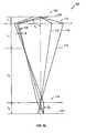
- FIG. 1shows a focused ion beam system in which a shaped ion beam can be produced and applied.
- FIGS. 2A and 2Bare ray diagrams of a focused ion beam column in accordance with an aperture imaging embodiment of the present invention.
- FIG. 2Ashows on the right side rays from a point source being imaged to the center of the second lens and shows on the left side rays from an extended source which graze the shaping aperture and pass through the second lens.
- FIG. 2Bshows the effects of chromatic and spherical aberrations on the rays on the left and right sides, respectively.
- FIG. 3is a ray diagram of a defocus embodiment for forming shaped beams.
- FIGS. 4A and 4Bare diagrams of rays emitted from a final lens toward a target, FIG. 4A showing rays without aberrations, and FIG. 4B is with substantial spherical aberrations.
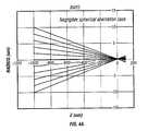
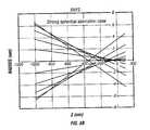
- FIGS. 5A , 5 B, and 5 Care graphs showing current density profiles across a focused ion beam at various target positions.
- FIG. 5Bis for the disk of least confusion target placement; and
- FIG. 5Cis for a large negative Z, where the beam is relatively uniform in current density.
- FIG. 6shows a straight aperture edge cutting off the beam along side the optical axis.
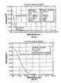
- FIG. 7is graph comparing the platinum deposition by the present invention and the prior art.
- an ion optical column in a focused ion beam systemproduces a shaped ion beam having one or more desirable geometric feature, such as a straight edge having sharp edge resolution.
- the ion optical columnis implemented in a focused ion beam system as described in FIG. 1 .
- an evacuated envelope 10includes an upper neck portion 12 within which are located a liquid metal ion source 14 and a focusing column 16 which includes extractor electrode means and an electrostatic optical system.
- Ion beam 18passes from source 14 through column 16 and between electrostatic deflection means schematically indicated at 20 toward sample 22 , which comprises, for example, a semiconductor device positioned on movable X-Y stage 24 within lower chamber 26 .
- An ion pump 28is employed for evacuating neck portion 12 .
- the chamber 26is evacuated with turbomolecular and mechanical pumping system 30 under the control of vacuum controller 32 .
- High voltage power supply 34is connected to liquid metal ion source 14 as well as to appropriate electrodes in focusing column 16 for forming an approximately 30 keV ion beam 18 and directing the same downwardly.
- Deflection controller and amplifier 36operated in accordance with a prescribed pattern such as a raster pattern provided by pattern generator 38 , is coupled to deflection plates 20 whereby beam 18 may be controlled to trace out a corresponding pattern on the upper surface of sample 22 .
- the deflection platesare placed before the final lens, as is well know in the art.
- the source 14typically provides a metal ion beam of gallium, although other ion sources, such as a multicusp or other plasma ion source, can be used.
- the sourcetypically is capable of being focused into a sub one-tenth micron wide beam at sample 22 for either modifying the surface 22 by ion milling, enhanced etch, material deposition, or for the purpose of imaging the surface 22 .
- An electron multiplier 40 used for detecting secondary emission for imagingis connected to video circuit and amplifier 42 , the latter supplying drive for video monitor 44 also receiving deflection signals from controller 36 .
- a gas source 46is located inwardly of the side of chamber 26 by translation device 48 adapted for positioning said source via support means within bellows 52 .
- U.S. Pat. No. 5,435,850 to Rasmussen for a “Gas Injection System” assigned to the assignee of the present inventiondiscloses an apparatus for introducing and directing gaseous vapor toward sample 22 .
- Source 46includes a reservoir 50 and a heater 54 , which may comprise a membrane type heater and which may be used for raising the temperature of a compound within reservoir 50 to a temperature for providing a suitable vapor pressure as hereinafter more fully disclosed.
- a transfer tube or nozzle 56comprising a capillary tube provided by a hypodermic needle extends from reservoir 50 and is connected thereto via control valve 58 adapted for releasing gaseous vapor.
- the nozzleis extended and translated in orthogonal directions substantially perpendicular to its axis employing translation apparatus 48 , so that gaseous vapor can be aimed directly toward a region on the top surface of sample 22 .
- a door 60is opened for inserting sample 22 on stage 24 which may be heated, and also for servicing the reservoir 50 .
- the dooris interlocked so that it cannot be opened if the temperature in reservoir 50 is substantially above room temperature.
- a gate valve, schematically illustrated at 62is closed before door 60 can be opened to seal off the ion source and focusing column apparatus.
- valve 58When reservoir 50 is raised to a desired temperature for vaporizing the compound within reservoir 50 , valve 58 may be opened by withdrawing an actuator rod from outside the apparatus to open and regulate the position of valve plunger, while the nozzle 56 is directed towards the desired area of the sample. Bellows 52 accommodates movement of the nozzle assembly and reservoir relative to the sample without affecting the vacuum within chamber 26 .
- the vacuum control systemalong with the heater of gaseous vapor source 46 are operated to provide an appropriate vapor pressure condition for establishing a gaseous vapor flux in chamber as directed toward substrate 22 for etching or depositing material.
- the reservoiris heated to a predetermined temperature.
- the high voltage power supplyprovides an appropriate acceleration voltage to electrodes in ion beam column 16 for energizing and focusing ion beam 18 .
- the ion beamprovides energy for initiating a reaction between the gaseous compound and the substrate and for either enhanced etching of or material deposition upon the sample.
- Deflection controller and amplifier 36causes the ion beam to be deflected in a desired pattern for etching sample 22 . Considerations regarding deflection speed, loop time, etc. are well understood by those skilled in the art.
- the vacuum systemprovides a vacuum of between approximately 1 ⁇ 10 ⁇ 7 Torr and 5 ⁇ 10 ⁇ 4 Torr within chamber 26 .
- the chamber background pressureis suitably about 1 ⁇ 10 ⁇ 5 Torr.
- the gaseous source 46is heated to a temperature for providing an appropriate gaseous flux via the capillary tube of the hypodermic needle, while the metal ion source and focusing column are suitably controlled for generating a corresponding appropriate ion flux. Skilled persons can readily determine appropriate pressures and gas flows for any particular application.
- the first preferred embodimentis referred to as the “aperture imaging” embodiment.
- the aperture imaging embodimentuses a two-lens ion focusing column, the first lens forming an image of the ion source at or near the plane of the second lens and the second lens forming an image on the target plane of a shaping aperture placed between the first and second lenses.
- Skilled personswill understand that the lenses and other “optical” elements used with focused ion beams use electrostatic or magnetic fields to control ions in the beam, and that the optical elements are controlling a stream of ions, not light.
- the designsmay include only one or up to several lenses.
- FIGS. 2A and 2Bare ray diagrams of a focused ion beam column 102 in accordance with an aperture imaging embodiment of the invention.
- Ion column 102includes a source 104 positioned on a source plane 106 .
- a first ion lens 112has a focal length F 1 and is positioned a distance F 1 from source plane 106 .
- a shaping aperture 114is positioned a distance L 1 from the plane of first lens 112 , and a second lens 116 having a focal length F 2 is located a distance L 2 from shaping aperture 114 .
- the magnification M 1 of the source by first lens 112is therefore (L 1 +L 2 )/F 1 and the magnification of the shaping aperture by second lens 116 is F 2 /L 2 .
- L 1is 35 mm
- L 2is 400 mm
- F 1is 25 mm
- F 2is 10 mm, giving an M 1 of 17 and an M 2 of 0.025.
- the ion column described aboveprovides an enlarged ion beam having a uniform current density at a target plane.
- the beamforms a reduced, that is, demagnified, image of the aperture at the target surface, the image having a high edge resolution value, that is, sharp or small edge widths.
- the impact spot of the ionsis in the shape of the aperture, with the ion bombardment rate being substantially uniform throughout the spot and dropping sharply to zero at the edge of the spot.
- Edge resolution of a shaped or unshaped beamcan be characterized in various ways, one way being the distance over which the beam current density falls from eighty-five percent of its maximum value to fifteen percent of that value.
- High edge resolutionis, for many applications, edge resolution on the order of a few tenths of microns or less, preferably less than one tenth of a micron, and more preferably less than fifty nanometers.
- the sharpness of the beam edgecorresponds to the edge width, W, of the image formed by the beam.
- a small edge widthcorresponds to a sharp edge and high resolution.
- the six primary factors that contribute to the edge width, Ware: the edge roughness of shaping aperture 114 , the spherical aberration of second lens 116 , the chromatic aberration of second lens 116 , the diffraction of second lens 116 , the interaction of ions within the beam, and the geometric aberration due to the extended source.
- the contribution to the edge width from each of these factorsis referred to as W A , W S , W C , W D , W B , and W G , respectively.
- the half-angle spread, A 2 , of ions leaving second lens 116is a factor in determining the contributions to the edge width of spherical aberration (W S ), chromatic aberration (W C ), and diffraction (W D ).
- the angular spread A 2is equal to the incoming angular spread, B, divided by the magnification M 2 .
- FIGS. 2A and 2Bshow factors contributing to the angular spread B.
- FIG. 2Ashows that rays 118 originating from a point in the center of ion source 104 and propagating in different directions are being imaged to the same point at the center of second lens 116 if no lens aberrations are present.
- the left hand side of FIG. 2Ashows that rays 120 originating from different points along source 104 and grazing shaping aperture 114 pass through second lens 116 at different points, thereby widening the beam at second lens 116 . Because second lens 22 is positioned to form an image of aperture 114 on a target plane 122 , rays 120 are focused to a single point (assuming no aberrations from the second lens), and the direct contribution to the edge width from the extended source (W G ) is zero. The extended source does, however, contribute to the angular spread, B, of ions entering second lens 116 .
- FIG. 2Bshows the effects of chromatic and spherical aberrations on the rays originating from the center of the source.
- Rays 128 a , 128 b , and 128 c on the left side of FIG. 1Bshow the effects of chromatic aberration, with ray 128 a having the nominal beam energy E, ray 128 b having energy E+dE, and ray 128 c having energy E ⁇ dE.
- Eis 30,000 V and dE is 5V.
- B Gr G /F 1 Eq. 2
- B SC S1 A 1 3 /F 1 Eq. 4
- r Gis source radius
- r Cis chromatic radius
- C C1is the coefficient of chromatic aberration of first lens 112
- C S1is the coefficient of chromatic aberration of first lens 112 .
- the spherical and chromatic aberration of second lens 116also contribute directly to the beam edge width.
- W Dthe contribution to the image edge width by diffraction, depends upon the wavelength and the second lens 116 entrance angle A 2 .
- W Athe contribution to the image edge width due to the demagnified aperture edge roughness is the dominant contribution.
- M 21/10
- W A0.2 ⁇ m, which is orders of magnitude greater than all other contributions to the edge width except the beam interaction contribution.
- Silicon or other semiconductor fabricated materialscould be used for the aperture and would provide a much smoother edge and, therefore, much better edge resolution. The edge of such apertures, however, would be rapidly milled away by the ion beam and frequent aperture changes would be necessary.
- W Bthe edge width contribution from beam interactions
- the beam interaction contributionis caused by ions in the beam repelling each other, particularly at points where the beam is narrowed over an extended distance. Beam interactions are a concern in this column design because the rays cross over in the center of second lens 116 , and the beam angle, B, is very shallow. Fortunately, the effect of the beam interactions on edge width is reduced because the crossover is late in the column.
- the 0.6 ⁇ m contribution to the edge width from the beam interactionsis less than the 2 ⁇ m from the aperture edge roughness.
- this estimateis low, as the beam interactions are stronger as the beam converges near second lens 116 , and extrapolating the orbits back to the aperture will then have a larger contribution.
- the approximation developed hereis rough in that an ion orbit is assumed to be perturbed from only one direction throughout the orbit.
- the contribution due to beam interactions in the shaped beam modecan be reduced by focusing the beam from first lens 112 slightly beyond the plane of second lens 116 . This would increase the beam diameter in second lens 116 and thereby decrease beam interactions. Second lens 116 aberrations would increase, but this could be tolerated as the column has extremely low spherical and chromatic aberration to begin with. These small aberrations from lens 2 result from the small beam size in the plane of the second lens 116 .
- the resulting edge resolutioncan be made sufficiently small using the aperture imaging embodiment to create a FIB having excellent edge resolution.
- This embodimentalso provides a uniform current density.
- Table 2gives various parameters described above as a function of the first lens 112 half-angle, A 1 . This table was calculated using the parameters of Table 1. The beam current in the last column of Table 2 is calculated using a source angular intensity of 20 microamps per steradian.
- the embodiment described abovehas the advantage that the shaped beam size is relatively independent of focus.
- the size of the shaped beamhowever, is relatively inflexible because the shaped beam forms an image of the aperture on the target plane and the size of the beam on the target plane is determined, therefore, by the size of the aperture and the demagnification from the aperture to the target plane.
- This embodimentis best suited for large, that is, tens of microns, sized beams. This is because a small aperture, which must be placed in a more dense beam, is quickly destroyed by that beam and a longer column to produce higher demagnification would adversely affect edge resolution by increasing beam interaction effects. Also, the range of useful aperture sizes is limited, because of the aperture edge width contribution, about two microns, from the electroetched apertures.
- edge roughnessis only one percent.
- a twenty micron aperturewould have ten percent edge roughness, and one hundred times less current would go through one aperture.
- a twenty micron aperturecould be fabricated from silicon, but it must be placed in a smaller, denser beam, and will erode very rapidly. Aperatures of various shapes can be used, depending on the application requirements.
- a second embodiment of the inventionis referred to the “defocusing” embodiment.
- Applicantshave discovered that if the chromatic aberration dominates over spherical aberration, a strongly underfocused ion beam will have a relatively uniform current density, and a straight-sided aperture in the beam path of such a beam will result in a beam having straight sides and sharp edges.
- a square or rectangular aperture placed in the beam path, preferably in the vicinity of the final lens, in combination with the strong under-focusingwill generate a square or rectangular beam.
- the defocusing embodimentuses a two lens column with a shaping aperture, and underfocuses the ion beam, an embodiment of which is shown in FIG. 3 .
- FIG. 3shows an ion source 140 , a first lens 142 , a second lens 144 , and a beam shaping aperture 146 .
- the targetis located in target plane 148 .
- FIG. 3also shows that second lens 144 converges ions onto a crossover point 152 below target plane 148 .
- the columnmay have substantial spherical aberration contribution, in this large under-focus condition, the beam is still relatively uniform in current density.
- a beamis “strongly” underfocused if the current density of the aberrated beam is relatively uniform throughout its cross section.
- FIGS. 4A and 4Bare ray diagrams showing rays, originally emitted from a point source, emerging from a final lens toward a target.
- FIG. 4Ashows rays 158 without aberrations, the rays converging to a point on a crossover plane.
- FIG. 4Bshows rays 160 having substantial spherical aberrations.
- Rays 160do not converge to a single point, as most of rays 160 cross the optical axis before reaching the target plane.
- a plane placed a distance Z from the crossover planewill have uniform current density over the beam.
- the spherical aberrated beam in FIG. 4Bhas a non-uniform current density, and for large negative Z, the rays tend to bunch up at the beam edges.
- there is a minimum beam diameter location 162called the disk of least confusion, at which the spherical aberrations produce non-uniformities over the entire beam.
- FIGS. 5A , 5 B, and 5 Cshow the calculated current density across unshaped (round) ion beams.
- the modified lenshas a focal length of about 20 mm for both the first and second lenses.
- FIGS. 5A and 5Bhave strong peaks in the current density and gaussian-like peak shapes or beam profiles. These types of beams have traditionally been employed in FIB systems.
- FIG. 5Cshows the current density at a target position having large underfocus or large negative Z ( ⁇ 1,000 ⁇ m), where the beam is relatively uniform in current density.
- FIG. 5C for the large under-focus conditionshows a relatively uniform current density over a large beam diameter with some increase in current density at the edges. Even though the column has substantial spherical aberration contribution, in this large under-focus condition, the beam is still relatively uniform in current density.
- FIG. 5Cshows that a square or rectangular aperture placed in the vicinity of the final lens in combination with the strong under-focusing will generate a square or rectangular beam.
- a beamis chromatic aberration limited if other sources of aberration are small compared to the chromatic aberration, that is, the chromatic aberration is the most significant factor preventing the ion beam from focusing to an ideal, first order image.
- the shaped beamwill have high edge resolution, that is, sharp edges or small edge widths.
- the chromatic aberrationbroadens the beam in proportion to the lens angle A, whereas the magnified source contribution is independent of A.
- FIG. 6shows a straight aperture edge cutting off the beam along two sides of the optical axis, which is perpendicular to the plane of the paper.
- rY 0 /cos( T ) Eq. 11
- AA 0 /cos( T ) Eq. 13
- Y 0is the distance of the straight, parallel aperture edges from the optical axis
- kis a constant
- T and rare variables used to describe different positions along the aperture edge
- a 0is the lens angle as determined by the aperture width.
- R CYis independent of T (or X), so the straight, parallel aperture sides give constant chromatic contribution in the Y-direction for the beam limited by the straight aperture edges.
- the chromatic aberrationis proportional to the aperture size Y 0 in FIG. 6 .
- the source contribution of Equation 16arises from the source being convoluted with a flat beam density having chromatic aberrated edges.
- the source contribution to the radiusis its diameter-hence the factor of 2.
- the, straight, parallel aperture sidesyield straight beam edges with constant chromatic and source contributions in the Y-direction for X from zero to infinity.
- the beam shaping apertureis shown placed before the final lens, though it could be placed before the first lens or elsewhere. If a straight aperture edge is placed in the X-direction a distance Y 0 from the beam optical axis in the Y-direction, then there is an angle A 0 of the beam in the Y-direction, which defines the chromatic aberration all along the X direction of the shaped beam independent of X. In other words, the beam cut by the straight aperture has a constant edge resolution. If a rectangular aperture is employed, then each side has a constant but different edge width, each width being defined by its Y 0 value and corresponding A 0 value.
- a special caseis where a square aperture is symmetrically placed about the beam axis, in which case all sides have the same edge resolution.
- a useful case for the rectangular apertureis where a slot must be cut with the ion beam, and a long, thin rectangular aperture can form a long, thin beam, with the long sides having sharper edges than the short sides.
- Equations similar to Equations 15 and 16can be derived for significant spherical aberration in the column by those skilled in the art.
- the aperture in this casecan be shaped along its edges to give a straight edged beam.
- Equation 15shows that the size of the shaped beam is proportional to A 0 and the defocus distance Z.
- this settingmust be to within a few microns in Z, which can be accomplished using, for example, a capacitance distance measuring device, such as manufactured by ADE Technology of Newton, Mass.
- a 00
- the chromatic term in the edge widthbecomes zero.
- Thiscan also be shown for spherical aberration.
- a center cut straight aperturehas the property that spherical and chromatic aberration do not contribute to the edge resolution of the beam. Remaining contributions to the beam resolution along this edge include the magnified source (See Equation 16) and the beam interactions.
- this methodcan be employed to sharpen a beam edge, though at the cost of reducing beam current.
- Low density ion beamscan be useful for FIB processing, where the ion beam and a gas jet are coincident upon the surface, to either enhance the etching or deposition of material on the surface.
- a prior art ion beamdepletes the adsorbed gas so fast that the chemistry is less effective.
- Either of these shaped beam methodscan be used in these applications to increase the process efficiency.
- An experimental exampleis shown in FIG. 7 , where platinum deposition speed is greatly increased using the defocus method to produce a less dense, shaped beam.
- the depositionactually goes from negative (milling the surface) to positive (deposition). This increased efficiency can give about 50 times increase in deposition throughput over normal deposition conditions using a less dense, lower current beam.
- shaped beamsare similar to electron beam lithography, where square or rectangular beams can be “stitched” together to form larger patterns.
- an array of edges or aperturescan be rapidly switched by mechanical or electrical (beam steering) means to mix and match beam strategies on the fly.
Landscapes
- Chemical & Material Sciences (AREA)
- Analytical Chemistry (AREA)
- Physics & Mathematics (AREA)
- Engineering & Computer Science (AREA)
- Plasma & Fusion (AREA)
- Drying Of Semiconductors (AREA)
- Physical Vapour Deposition (AREA)
Abstract
Description
B=(BG2+BC2+BS2)0.5 Eq. 1
BG=rG/F1 Eq. 2
BC=rC/F1=CC1A1e/F1 Eq. 3
BS=CS1A13/F1 Eq. 4
| TABLE 1 | |
| CC1 = | 100 mm |
| CS1 = | 500 mm |
| F1 = | 25 |
| F | |
| 2 = | 10 mm |
| rG = | 0.05 mm |
| RC = | 25 nm |
Thus, chromatic and spherical aberrations of
DB=(3.122−2.742)0.5=1.49 μm Eq. 5
for the beam focused by the first lens to the plane of the second lens. One method of determining the contribution of the beam interactions to the final beam edge width is to estimate what deviation these rays have when extrapolated back to the aperture. Assume that the deviation of individual particles from straight lines has column length dependence as follows:
Db=K ZN Eq. 6
where Z is the beam interaction length and K and N are parameters. Differentiating to get the slope of the ray at distance Z gives:
dDb/dZ=N K ZN−1 Eq. 7
Then the ray deviation extrapolated back to Z=0 is
Db0=(dDb/dZ)Z−Db=(N−1)Db Eq. 8
W. Stickel, in “Simulation of Coulomb Interactions in electron Beam Lithography Systems—A Comparison of Theoretical Models”, Papers from the 42ndInternational Conference on Electron, Ion, and Photon Beam Technology and Nanofabrication, 26-29 May 1998, Chicago, Ill., suggests that N=1.4, and in this case,
Dbo=0.4Db=0.6 μm Eq. 9
| TABLE 2 | ||||||||||||||
| A1 | BG | BC | BS | B | A2 | WC | WS | WD | WA | WB | W | Ib | ||
| (rad) | M1 | (rad) | (rad) | (rad) | (rad) | M2 | (rad) | (um) | (um) | (um) | (um) | (um) | (um) | (nA) |
| 0.002 | 17.00 | 2.0E-06 | 1.3E-06 | 1.6E-07 | 2.4E-06 | 0.025 | 9.6E-05 | 1.6E-06 | 4.5E-10 | 2.1E-04 | 5.0E-02 | 0.05 | 0.628 | |
| 0.004 | 17.00 | 2.0E-06 | 2.7E-06 | 1.3E-06 | 3.6E-06 | 0.025 | 1.4E-04 | 2.4E-06 | 1.5E-09 | 1.4E-04 | 5.0E-02 | 0.05 | 2.512 | |
| 0.006 | 17.00 | 2.0E-06 | 4.0E-06 | 4.3E-06 | 6.2E-06 | 0.025 | 2.5E-04 | 4.1E-06 | 7.7E-09 | 8.0E-05 | 5.0E-02 | 0.05 | 5.652 | |
| 0.008 | 17.00 | 2.0E-06 | 5.3E-06 | 1.0E-05 | 1.2E-05 | 0.025 | 4.7E-04 | 7.8E-06 | 5.1E-08 | 4.3E-05 | 5.0E-02 | 0.05 | 10.048 | |
| 0.010 | 17.00 | 2.0E-06 | 6.7E-06 | 2.0E-05 | 2.1E-05 | 0.025 | 8.5E-04 | 1.4E-05 | 3.0E-07 | 2.4E-05 | 5.0E-02 | 0.05 | 15.700 | |
| 0.012 | 17.00 | 2.0E-06 | 8.0E-06 | 3.5E-05 | 3.6E-05 | 0.025 | 1.4E-03 | 2.4E-05 | 1.4E-06 | 1.4E-05 | 5.0E-02 | 0.05 | 22.608 | |
| 0.014 | 17.00 | 2.0E-06 | 9.3E-06 | 5.5E-05 | 5.6E-05 | 0.025 | 2.2E-03 | 3.7E-05 | 5.5E-06 | 9.0E-06 | 5.0E-02 | 0.05 | 30.772 | |
| 0.016 | 17.00 | 2.0E-06 | 1.1E-05 | 8.2E-05 | 8.3E-05 | 0.025 | 3.3E-03 | 5.5E-05 | 1.8E-05 | 6.1E-06 | 5.0E-02 | 0.05 | 40.192 | |
| 0.018 | 17.00 | 2.0E-06 | 1.2E-05 | 1.2E-04 | 1.2E-04 | 0.025 | 4.7E-03 | 7.8E-05 | 5.2E-05 | 4.3E-06 | 5.0E-02 | 0.05 | 50.868 | |
| 0.020 | 17.00 | 2.0E-06 | 1.3E-05 | 1.6E-04 | 1.6E-04 | 0.025 | 6.4E-03 | 1.1E-04 | 1.3E-04 | 3.1E-06 | 5.0E-02 | 0.05 | 62.800 | |
| 0.022 | 17.00 | 2.0E-06 | 1.5E-05 | 2.1E-04 | 2.1E-04 | 0.025 | 8.5E-03 | 1.4E-04 | 3.1E-04 | 2.3E-06 | 5.0E-02 | 0.05 | 75.988 | |
| 0.024 | 17.00 | 2.0E-05 | 1.6E-05 | 2.8E-04 | 2.8E-04 | 0.025 | 1.1E-02 | 1.8E-04 | 6.8E-04 | 1.8E-06 | 5.0E-02 | 0.05 | 90.432 | |
| 0.026 | 17.00 | 2.0E-06 | 1.7E-05 | 3.5E-04 | 3.5E-04 | 0.025 | 1.4E-02 | 2.3E-04 | 1.4E-03 | 1.4E-06 | 5.0E-02 | 0.05002 | 106.132 | |
| 0.028 | 17.00 | 2.0E-06 | 1.9E-05 | 4.4E-04 | 4.4E-04 | 0.025 | 1.8E-02 | 2.9E-04 | 2.7E-03 | 1.1E-06 | 5.0E-02 | 0.05007 | 123.088 | |
| 0.030 | 17.00 | 2.0E-06 | 2.0E-05 | 5.4E-04 | 5.4E-04 | 0.025 | 2.2E-02 | 3.6E-04 | 5.0E-03 | 9.3E-07 | 5.0E-02 | 0.05026 | 141.300 | |
RC=(CC(dE/E)+Z)A Eq. 10
where RCis the chromatic radius, CCis the chromatic aberration coefficient, dE/E is the normalized energy spread, and Z is the image plane distance away from the first order focal plane (positive Z is in the direction away from the final lens).
r=Y0/cos(T) Eq. 11
A=k r=k Y0/cos(T) Eq. 12
A=A0/cos(T) Eq. 13
RCY=RCcos(T)=CC(dE/E)A0 Eq. 14
WY=Z A0 Eq. 15
and
dWY=(CC(dE/E)A0)2+(2M RG)2)1/2 Eq. 16
where WYis the beam half-width in the Y direction, and dWYis the beam edge width in the Y-direction, and it is assumed that the beam is strongly under-focused (Z<<0). The source contribution of
Claims (29)
Priority Applications (2)
| Application Number | Priority Date | Filing Date | Title |
|---|---|---|---|
| US09/765,806US6949756B2 (en) | 2000-01-21 | 2001-01-19 | Shaped and low density focused ion beams |
| US10/688,810US6977386B2 (en) | 2001-01-19 | 2003-10-17 | Angular aperture shaped beam system and method |
Applications Claiming Priority (2)
| Application Number | Priority Date | Filing Date | Title |
|---|---|---|---|
| US17751800P | 2000-01-21 | 2000-01-21 | |
| US09/765,806US6949756B2 (en) | 2000-01-21 | 2001-01-19 | Shaped and low density focused ion beams |
Related Child Applications (1)
| Application Number | Title | Priority Date | Filing Date |
|---|---|---|---|
| US10/688,810Continuation-In-PartUS6977386B2 (en) | 2001-01-19 | 2003-10-17 | Angular aperture shaped beam system and method |
Publications (2)
| Publication Number | Publication Date |
|---|---|
| US20010045525A1 US20010045525A1 (en) | 2001-11-29 |
| US6949756B2true US6949756B2 (en) | 2005-09-27 |
Family
ID=22648901
Family Applications (1)
| Application Number | Title | Priority Date | Filing Date |
|---|---|---|---|
| US09/765,806Expired - LifetimeUS6949756B2 (en) | 2000-01-21 | 2001-01-19 | Shaped and low density focused ion beams |
Country Status (5)
| Country | Link |
|---|---|
| US (1) | US6949756B2 (en) |
| EP (1) | EP1210723B1 (en) |
| JP (1) | JP5259035B2 (en) |
| DE (1) | DE60138002D1 (en) |
| WO (1) | WO2001054163A1 (en) |
Cited By (10)
| Publication number | Priority date | Publication date | Assignee | Title |
|---|---|---|---|---|
| US20060060777A1 (en)* | 2004-09-07 | 2006-03-23 | Canon Kabushiki Kaisha | Apparatus and method for evaluating cross section of specimen |
| US20060250147A1 (en)* | 2003-08-26 | 2006-11-09 | Yukihiro Morita | Insulating film measuring device, insulating film measuring method, insulating film evaluating device, insulating film evaluating method, substrate for electric discharge display element, and plasma display panel |
| US20080073587A1 (en)* | 2006-02-15 | 2008-03-27 | Fei Company | Sputtering coating of protective layer for charged particle beam processing |
| US20090133167A1 (en)* | 2007-11-21 | 2009-05-21 | Fei Company | Method for obtaining a scanning transmission image of a sample in a particle-optical apparatus |
| US20090220561A1 (en)* | 2005-04-28 | 2009-09-03 | Sungho Jin | Compositions comprising nanostructures for cell, tissue and artificial organ growth, and methods for making and using same |
| US20110085968A1 (en)* | 2009-10-13 | 2011-04-14 | The Regents Of The University Of California | Articles comprising nano-materials for geometry-guided stem cell differentiation and enhanced bone growth |
| US8653474B2 (en) | 2003-10-17 | 2014-02-18 | Fei Company | Charged particle extraction device and method of design there for |
| EP3166127A1 (en) | 2015-10-30 | 2017-05-10 | FEI Company | Method for optimizing charged particle beams formed by shaped apertures |
| EP4297062A1 (en) | 2022-06-23 | 2023-12-27 | Fei Company | Focused ion beam system and method |
| US12253391B2 (en) | 2018-05-24 | 2025-03-18 | The Research Foundation For The State University Of New York | Multielectrode capacitive sensor without pull-in risk |
Families Citing this family (17)
| Publication number | Priority date | Publication date | Assignee | Title |
|---|---|---|---|---|
| FR2806527B1 (en) | 2000-03-20 | 2002-10-25 | Schlumberger Technologies Inc | SIMULTANEOUS FOCUSING COLUMN OF PARTICLE BEAM AND OPTICAL BEAM |
| US6921722B2 (en)* | 2000-05-30 | 2005-07-26 | Ebara Corporation | Coating, modification and etching of substrate surface with particle beam irradiation of the same |
| US20060051508A1 (en)* | 2000-12-28 | 2006-03-09 | Ilan Gavish | Focused ion beam deposition |
| US6638580B2 (en)* | 2000-12-29 | 2003-10-28 | Intel Corporation | Apparatus and a method for forming an alloy layer over a substrate using an ion beam |
| US6492261B2 (en)* | 2000-12-30 | 2002-12-10 | Intel Corporation | Focused ion beam metal deposition |
| US6977386B2 (en)* | 2001-01-19 | 2005-12-20 | Fei Company | Angular aperture shaped beam system and method |
| US7160475B2 (en)* | 2002-11-21 | 2007-01-09 | Fei Company | Fabrication of three dimensional structures |
| US6926935B2 (en)* | 2003-06-27 | 2005-08-09 | Fei Company | Proximity deposition |
| FR2859488B1 (en)* | 2003-09-10 | 2006-02-17 | Centre Nat Rech Scient | PROCESS FOR PRODUCING AT LEAST ONE CAVITY IN A MATERIAL |
| JP5509239B2 (en)* | 2004-09-29 | 2014-06-04 | 株式会社日立ハイテクノロジーズ | Ion beam processing apparatus and processing method |
| JP5033314B2 (en)* | 2004-09-29 | 2012-09-26 | 株式会社日立ハイテクノロジーズ | Ion beam processing apparatus and processing method |
| WO2011163397A1 (en) | 2010-06-22 | 2011-12-29 | The Regents Of The University Of California | Microfabricated high-bandpass foucault aperture for electron microscopy |
| JP6403200B2 (en) | 2014-12-03 | 2018-10-10 | 日本電子株式会社 | Film forming method and focused ion beam apparatus |
| JP2017020106A (en)* | 2015-07-02 | 2017-01-26 | エフ・イ−・アイ・カンパニー | Adaptive beam current for high-throughput pattern formation |
| JP7154593B2 (en)* | 2019-02-15 | 2022-10-18 | 株式会社日立ハイテクサイエンス | COMPOSITE CHARGED PARTICLE BEAM DEVICE AND CONTROL METHOD |
| US10971618B2 (en) | 2019-08-02 | 2021-04-06 | Applied Materials Israel Ltd. | Generating milled structural elements with a flat upper surface |
| US12205789B1 (en) | 2023-07-22 | 2025-01-21 | New York Structural Biology Center | Transmission electron microscopy with square beams |
Citations (45)
| Publication number | Priority date | Publication date | Assignee | Title |
|---|---|---|---|---|
| JPS6169125A (en) | 1984-08-06 | 1986-04-09 | Nippon Telegr & Teleph Corp <Ntt> | Charged beam exposure equipment |
| US4609809A (en) | 1983-03-16 | 1986-09-02 | Hitachi, Ltd. | Method and apparatus for correcting delicate wiring of IC device |
| US4634871A (en) | 1985-01-14 | 1987-01-06 | Hughes Aircraft Company | Method and apparatus for spot shaping and blanking a focused beam |
| US4661709A (en) | 1985-06-28 | 1987-04-28 | Control Data Corporation | Modular all-electrostatic electron-optical column and assembly of said columns into an array and method of manufacture |
| US4694178A (en) | 1985-06-28 | 1987-09-15 | Control Data Corporation | Multiple channel electron beam optical column lithography system and method of operation |
| US4698236A (en)* | 1984-10-26 | 1987-10-06 | Ion Beam Systems, Inc. | Augmented carbonaceous substrate alteration |
| US4724359A (en)* | 1986-10-17 | 1988-02-09 | General Electric Company | Laminar flow guns for light valves |
| US4820898A (en) | 1986-08-27 | 1989-04-11 | U.S. Philips Corporation | Ion beam apparatus for finishing patterns |
| US4874460A (en) | 1987-11-16 | 1989-10-17 | Seiko Instruments Inc. | Method and apparatus for modifying patterned film |
| US4876112A (en) | 1986-05-29 | 1989-10-24 | Seiko Instruments Inc. | Process for forming metallic patterned film |
| US4894549A (en) | 1987-03-05 | 1990-01-16 | Ims Ionen Mikrofabrikations Systeme Gesellschaft M.B.H. | Apparatus for demagnification or full-size ion projection lithography |
| USRE33193E (en)* | 1981-09-30 | 1990-04-03 | Hitachi, Ltd. | Ion beam processing apparatus and method of correcting mask defects |
| DE3910054A1 (en) | 1989-03-28 | 1990-10-11 | Siemens Ag | ION IMPLANTATION SYSTEM |
| US5051556A (en) | 1988-10-31 | 1991-09-24 | Fujitsu Limited | Charged particle beam lithography system and a method thereof |
| US5061850A (en)* | 1990-07-30 | 1991-10-29 | Wisconsin Alumni Research Foundation | High-repetition rate position sensitive atom probe |
| US5093572A (en) | 1989-11-02 | 1992-03-03 | Mitsubishi Denki Kabushiki Kaisha | Scanning electron microscope for observation of cross section and method of observing cross section employing the same |
| US5120925A (en)* | 1989-05-10 | 1992-06-09 | Hitachi, Ltd. | Methods for device transplantation |
| US5126287A (en)* | 1990-06-07 | 1992-06-30 | Mcnc | Self-aligned electron emitter fabrication method and devices formed thereby |
| US5149974A (en) | 1990-10-29 | 1992-09-22 | International Business Machines Corporation | Gas delivery for ion beam deposition and etching |
| US5151605A (en)* | 1990-04-09 | 1992-09-29 | U.S. Philips Corporation | Method of irradiating an object by means of a charged particle beam, and device for performing the method |
| US5188705A (en) | 1991-04-15 | 1993-02-23 | Fei Company | Method of semiconductor device manufacture |
| US5376791A (en) | 1991-04-15 | 1994-12-27 | Fei Company | Secondary ion mass spectometry system |
| US5389196A (en)* | 1992-01-30 | 1995-02-14 | Massachusetts Institute Of Technology | Methods for fabricating three-dimensional micro structures |
| US5435850A (en) | 1993-09-17 | 1995-07-25 | Fei Company | Gas injection system |
| US5524018A (en)* | 1993-10-04 | 1996-06-04 | Adachi; Yoshi | Superior resolution laser using bessel transform optical filter |
| US5574280A (en) | 1993-03-02 | 1996-11-12 | Seiko Instruments Inc. | Focused ion beam apparatus and method |
| US5583344A (en)* | 1993-03-10 | 1996-12-10 | Hitachi, Ltd. | Process method and apparatus using focused ion beam generating means |
| US5827786A (en) | 1994-06-28 | 1998-10-27 | Fei Company | Charged particle deposition of electrically insulating films |
| US5852297A (en)* | 1995-03-24 | 1998-12-22 | Ishitani; Tohru | Focused ion beam apparatus and method for irradiating focused ion beam |
| US5916424A (en)* | 1996-04-19 | 1999-06-29 | Micrion Corporation | Thin film magnetic recording heads and systems and methods for manufacturing the same |
| EP0927880A1 (en) | 1997-07-22 | 1999-07-07 | Hitachi, Ltd. | Method and apparatus for preparing samples |
| US5945677A (en) | 1998-04-10 | 1999-08-31 | The Regents Of The University Of California | Focused ion beam system |
| US5952658A (en)* | 1996-04-18 | 1999-09-14 | Hitachi, Ltd. | Method and system for judging milling end point for use in charged particle beam milling system |
| US5973295A (en)* | 1993-07-30 | 1999-10-26 | International Business Machines Corporation | Heated tool positioned in the X,Y, and 2-directions for depositing fine lines on a substrate |
| US6011269A (en) | 1998-04-10 | 2000-01-04 | Etec Systems, Inc. | Shaped shadow projection for an electron beam column |
| US6042738A (en)* | 1997-04-16 | 2000-03-28 | Micrion Corporation | Pattern film repair using a focused particle beam system |
| US6048588A (en)* | 1988-07-08 | 2000-04-11 | Cauldron Limited Partnership | Method for enhancing chemisorption of material |
| US6118129A (en)* | 1994-03-15 | 2000-09-12 | Fujitsu Limited | Method and system for exposing an exposure pattern on an object by a charged particle beam which is shaped into a plurality of beam elements |
| US6128134A (en)* | 1997-08-27 | 2000-10-03 | Digital Optics Corporation | Integrated beam shaper and use thereof |
| WO2000075954A2 (en) | 1999-06-09 | 2000-12-14 | Etec Systems, Inc. | Apparatus and method for forming a charged particle beam of arbitrary shape |
| US6177670B1 (en)* | 1998-01-23 | 2001-01-23 | Seiko Instruments Inc. | Method of observing secondary ion image by focused ion beam |
| US6274877B1 (en)* | 1997-05-08 | 2001-08-14 | Canon Kabushiki Kaisha | Electron beam exposure apparatus |
| US6277542B1 (en)* | 1998-06-05 | 2001-08-21 | Nikon Corporation | Charged-particle-beam projection-exposure methods exhibiting more uniform beam-current density |
| US6303932B1 (en)* | 1997-11-20 | 2001-10-16 | Hitachi, Ltd. | Method and its apparatus for detecting a secondary electron beam image and a method and its apparatus for processing by using focused charged particle beam |
| US6414307B1 (en)* | 1999-07-09 | 2002-07-02 | Fei Company | Method and apparatus for enhancing yield of secondary ions |
Family Cites Families (6)
| Publication number | Priority date | Publication date | Assignee | Title |
|---|---|---|---|---|
| US4687940A (en)* | 1986-03-20 | 1987-08-18 | Hughes Aircraft Company | Hybrid focused-flood ion beam system and method |
| JPH09199072A (en)* | 1996-01-22 | 1997-07-31 | Hitachi Ltd | Ion beam projection method and apparatus |
| JPH10144583A (en)* | 1996-11-07 | 1998-05-29 | Nikon Corp | Charged particle beam projection method and charged particle beam projection apparatus |
| JPH10162769A (en)* | 1996-11-28 | 1998-06-19 | Hitachi Ltd | Ion beam processing equipment |
| JPH1177333A (en)* | 1997-09-09 | 1999-03-23 | Hitachi Ltd | Focused ion beam processing apparatus and method |
| JP3542140B2 (en)* | 1997-09-10 | 2004-07-14 | 株式会社日立製作所 | Projection type ion beam processing equipment |
- 2001
- 2001-01-19WOPCT/EP2001/000621patent/WO2001054163A1/enactiveApplication Filing
- 2001-01-19EPEP01903662Apatent/EP1210723B1/ennot_activeExpired - Lifetime
- 2001-01-19JPJP2001553556Apatent/JP5259035B2/ennot_activeExpired - Fee Related
- 2001-01-19DEDE60138002Tpatent/DE60138002D1/ennot_activeExpired - Lifetime
- 2001-01-19USUS09/765,806patent/US6949756B2/ennot_activeExpired - Lifetime
Patent Citations (47)
| Publication number | Priority date | Publication date | Assignee | Title |
|---|---|---|---|---|
| USRE33193E (en)* | 1981-09-30 | 1990-04-03 | Hitachi, Ltd. | Ion beam processing apparatus and method of correcting mask defects |
| US4609809A (en) | 1983-03-16 | 1986-09-02 | Hitachi, Ltd. | Method and apparatus for correcting delicate wiring of IC device |
| US4609809B1 (en) | 1983-03-16 | 1993-01-26 | Hitachi Ltd | |
| JPS6169125A (en) | 1984-08-06 | 1986-04-09 | Nippon Telegr & Teleph Corp <Ntt> | Charged beam exposure equipment |
| US4698236A (en)* | 1984-10-26 | 1987-10-06 | Ion Beam Systems, Inc. | Augmented carbonaceous substrate alteration |
| US4634871A (en) | 1985-01-14 | 1987-01-06 | Hughes Aircraft Company | Method and apparatus for spot shaping and blanking a focused beam |
| US4661709A (en) | 1985-06-28 | 1987-04-28 | Control Data Corporation | Modular all-electrostatic electron-optical column and assembly of said columns into an array and method of manufacture |
| US4694178A (en) | 1985-06-28 | 1987-09-15 | Control Data Corporation | Multiple channel electron beam optical column lithography system and method of operation |
| US4876112A (en) | 1986-05-29 | 1989-10-24 | Seiko Instruments Inc. | Process for forming metallic patterned film |
| EP0257685B1 (en) | 1986-08-27 | 1991-01-09 | Koninklijke Philips Electronics N.V. | Method for altering patterns provided at a surface of a carrier and apparatus for carrying it out |
| US4820898A (en) | 1986-08-27 | 1989-04-11 | U.S. Philips Corporation | Ion beam apparatus for finishing patterns |
| US4724359A (en)* | 1986-10-17 | 1988-02-09 | General Electric Company | Laminar flow guns for light valves |
| US4894549A (en) | 1987-03-05 | 1990-01-16 | Ims Ionen Mikrofabrikations Systeme Gesellschaft M.B.H. | Apparatus for demagnification or full-size ion projection lithography |
| US4874460A (en) | 1987-11-16 | 1989-10-17 | Seiko Instruments Inc. | Method and apparatus for modifying patterned film |
| US6048588A (en)* | 1988-07-08 | 2000-04-11 | Cauldron Limited Partnership | Method for enhancing chemisorption of material |
| US5051556A (en) | 1988-10-31 | 1991-09-24 | Fujitsu Limited | Charged particle beam lithography system and a method thereof |
| DE3910054A1 (en) | 1989-03-28 | 1990-10-11 | Siemens Ag | ION IMPLANTATION SYSTEM |
| US5120925A (en)* | 1989-05-10 | 1992-06-09 | Hitachi, Ltd. | Methods for device transplantation |
| US5093572A (en) | 1989-11-02 | 1992-03-03 | Mitsubishi Denki Kabushiki Kaisha | Scanning electron microscope for observation of cross section and method of observing cross section employing the same |
| US5151605A (en)* | 1990-04-09 | 1992-09-29 | U.S. Philips Corporation | Method of irradiating an object by means of a charged particle beam, and device for performing the method |
| US5126287A (en)* | 1990-06-07 | 1992-06-30 | Mcnc | Self-aligned electron emitter fabrication method and devices formed thereby |
| US5061850A (en)* | 1990-07-30 | 1991-10-29 | Wisconsin Alumni Research Foundation | High-repetition rate position sensitive atom probe |
| US5149974A (en) | 1990-10-29 | 1992-09-22 | International Business Machines Corporation | Gas delivery for ion beam deposition and etching |
| US5188705A (en) | 1991-04-15 | 1993-02-23 | Fei Company | Method of semiconductor device manufacture |
| US5376791A (en) | 1991-04-15 | 1994-12-27 | Fei Company | Secondary ion mass spectometry system |
| US5389196A (en)* | 1992-01-30 | 1995-02-14 | Massachusetts Institute Of Technology | Methods for fabricating three-dimensional micro structures |
| US5574280A (en) | 1993-03-02 | 1996-11-12 | Seiko Instruments Inc. | Focused ion beam apparatus and method |
| US5583344A (en)* | 1993-03-10 | 1996-12-10 | Hitachi, Ltd. | Process method and apparatus using focused ion beam generating means |
| US5973295A (en)* | 1993-07-30 | 1999-10-26 | International Business Machines Corporation | Heated tool positioned in the X,Y, and 2-directions for depositing fine lines on a substrate |
| US5435850A (en) | 1993-09-17 | 1995-07-25 | Fei Company | Gas injection system |
| US5524018A (en)* | 1993-10-04 | 1996-06-04 | Adachi; Yoshi | Superior resolution laser using bessel transform optical filter |
| US6118129A (en)* | 1994-03-15 | 2000-09-12 | Fujitsu Limited | Method and system for exposing an exposure pattern on an object by a charged particle beam which is shaped into a plurality of beam elements |
| US5827786A (en) | 1994-06-28 | 1998-10-27 | Fei Company | Charged particle deposition of electrically insulating films |
| US5852297A (en)* | 1995-03-24 | 1998-12-22 | Ishitani; Tohru | Focused ion beam apparatus and method for irradiating focused ion beam |
| US5952658A (en)* | 1996-04-18 | 1999-09-14 | Hitachi, Ltd. | Method and system for judging milling end point for use in charged particle beam milling system |
| US5916424A (en)* | 1996-04-19 | 1999-06-29 | Micrion Corporation | Thin film magnetic recording heads and systems and methods for manufacturing the same |
| US6042738A (en)* | 1997-04-16 | 2000-03-28 | Micrion Corporation | Pattern film repair using a focused particle beam system |
| US6274877B1 (en)* | 1997-05-08 | 2001-08-14 | Canon Kabushiki Kaisha | Electron beam exposure apparatus |
| EP0927880A1 (en) | 1997-07-22 | 1999-07-07 | Hitachi, Ltd. | Method and apparatus for preparing samples |
| US6128134A (en)* | 1997-08-27 | 2000-10-03 | Digital Optics Corporation | Integrated beam shaper and use thereof |
| US6303932B1 (en)* | 1997-11-20 | 2001-10-16 | Hitachi, Ltd. | Method and its apparatus for detecting a secondary electron beam image and a method and its apparatus for processing by using focused charged particle beam |
| US6177670B1 (en)* | 1998-01-23 | 2001-01-23 | Seiko Instruments Inc. | Method of observing secondary ion image by focused ion beam |
| US5945677A (en) | 1998-04-10 | 1999-08-31 | The Regents Of The University Of California | Focused ion beam system |
| US6011269A (en) | 1998-04-10 | 2000-01-04 | Etec Systems, Inc. | Shaped shadow projection for an electron beam column |
| US6277542B1 (en)* | 1998-06-05 | 2001-08-21 | Nikon Corporation | Charged-particle-beam projection-exposure methods exhibiting more uniform beam-current density |
| WO2000075954A2 (en) | 1999-06-09 | 2000-12-14 | Etec Systems, Inc. | Apparatus and method for forming a charged particle beam of arbitrary shape |
| US6414307B1 (en)* | 1999-07-09 | 2002-07-02 | Fei Company | Method and apparatus for enhancing yield of secondary ions |
Non-Patent Citations (20)
| Title |
|---|
| "Plasma Ion Source-ECR microwave plasma ion source," http://www.tectra.de/plasma-ion-source.htm, Feb. 18, 2000 Contact: Dr. Christian Bradley, tectra GmbH, Reuterweg 65, D-60323 Frankfurt/M. |
| Bauer, E., Koziol, C., Lilienkamp, G., Schmidt, T., "Spectromicroscopy in a Low Energy Electron Microscope," Journal of Electron Spectroscopy and Related Phenomena 84 (1997) pp 201-209. |
| Edinger, Klaus and Kraus, Thomas, "Modeling of Focused Ion Beam Induced Surface Chemistry," Journal of Vacuum Science Technology B 18(6), Nov./Dec. 2000; pp 3190-3193. |
| Edinger, Klaus, Yun, Victor, Melngaillis, John and Orloff, Jon, "Development of a High Brightness Gas Field Ion Source," J. Vac. Sci. Technol. b(6), Nov./Dec. 1997, pp. 2365-2368. |
| Guharay, S.K., Wang, W., Dudnikov, V.G., Reiser,M. Orloff,J. And Meingaillis, J., "High-brightness Ion Source for Ion Projection Lithography," J. Vac. Sci. Technol. B(6), Nov./Dec. 1996, pp. 3907-3910. |
| Hawkes, P.W. and Kasper, E., Principles of Electron Optics, vol. 2., Applied Geometrical Optics, Academic Press, 1989: Chapters 47, 48. pp 971-1003. |
| Lee, Y. ,et al. "Development of Ion Sources for Ion Projection Lithography" Journal of Vacuum Science Technology, B 14(6), Nov./Dec. 1996; pp 3947-3950. |
| Orloff, J., and Sudraud, Pierre, "Design of a 100 kV, High Resolution Focused Ion Beam Column with a Liquid Metal Ion Source" Microelectronic Engineering 3 (1985)pp. 161-165. |
| Orloff, J., and Swanson, L. W., "Some Considerations on the Design of a Field Emission Gun for a Shaped Spit Lithography System," Optik, vol. 61, No. 3 (1982), pp 237-245. |
| Orloff, J., Li, J. Z., Sato, M., "Experimental Study of a Focused Ion Beam Probe Size and Comparison with Theory," Journal of Vacuum Science Technology, B 9 (5), Sep./Oct. 1991, pp 2609-2612. |
| Sato, M., and Orloff, J. "A Method for calculating the Current Density of Charged Particle Beams and the Effect of Finite Source Size and Spherical and Chromatic Aberrations on the Focusing Characteristics," Journal of Vacuum Science Technology, B, vol 9, No. 5, Sep./Oct. 1991; pp 2602-2608. |
| Slingerland, H. N., "Optimization of a Chromatically Limited Ion Microprobe," Microelectronic Engineering 2 (1984) 219-226. |
| Slingerland, H.N., Barth, J.E., Koets, E. Kramer, J. van der Mast, K.D., "Proposal for a Second Generation IBPG," Proceedings Microcircuit Engineering Conference, 1984, Microcircuit Engineering, 1985, pp. 381-387. |
| Slingerland, H.N., Bohlander, J.H., van der Mast, K.D., Koets, E., "Progress on the Delft Ion Beam Pattern Generator," Microelectronic Engineering 5 (1986), Elsevier Science Publishers B.V. (North Holland), pp 155-161. |
| Stickel, W., "Simulation of Columb Interactions in Electron Beam Lithography Systems-A Comparison of Theoretical Models," Papers from the 42<SUP>nd </SUP>International Conference on Electron, Ion, and Photon Beam Technology and Nanofabrication, May 26-29, 1998. |
| Tuggle, D.W., Swanson, L.W., and Gesley, M.A., "Current Distribution in a Chromatically Limited Electron Microprobe", J. Vac. Sci. Technol. B4 (1) Jan./Feb. 1986 pp. 131-134. |
| Van der Mast, K.D., Jansen, G.H., Barth, J.E., "The Shower-Beam Concept" Microelectronic Engineering 3 (1985), Elsevier Science Publishers B.V. (North Holland), pp 43-51. |
| Van der Mast, K.D., Pijper, F. J., and Barth, J.E., "A Flexible Beamshaper," Microelectronic Engineering 5 (1986), Elsevier Science Publishers B.V. (North Holland), pp 115-122. |
| Vijgen, L., "Coulomb Interactions in Focused Ion Beam Columns," 3 Beams Conference 1992. |
| Vijgen, L.J., and Kruit, P., "Coulomb Interactions in a Shaped Ion Beam Pattern Generator," J. Vac. Sci. Technol. B 10(6), Nov./Dec. 1992, pp. 2809-2813. |
Cited By (19)
| Publication number | Priority date | Publication date | Assignee | Title |
|---|---|---|---|---|
| US20060250147A1 (en)* | 2003-08-26 | 2006-11-09 | Yukihiro Morita | Insulating film measuring device, insulating film measuring method, insulating film evaluating device, insulating film evaluating method, substrate for electric discharge display element, and plasma display panel |
| US8653474B2 (en) | 2003-10-17 | 2014-02-18 | Fei Company | Charged particle extraction device and method of design there for |
| US7297947B2 (en)* | 2004-09-07 | 2007-11-20 | Canon Kabushiki Kaisha | Apparatus and method for evaluating cross section of specimen |
| US20060060777A1 (en)* | 2004-09-07 | 2006-03-23 | Canon Kabushiki Kaisha | Apparatus and method for evaluating cross section of specimen |
| US8414908B2 (en) | 2005-04-28 | 2013-04-09 | The Regents Of The University Of California | Compositions comprising nanostructures for cell, tissue and artificial organ growth, and methods for making and using same |
| US9844657B2 (en) | 2005-04-28 | 2017-12-19 | The Regents Of The University Of California | Compositions comprising nanostructures for cell, tissue and artificial organ growth, and methods for making and using same |
| US10518074B2 (en) | 2005-04-28 | 2019-12-31 | The Regents Of The University Of California | Compositions comprising nanostructures for cell, tissue and artificial organ growth, and methods for making and using same |
| US20090220561A1 (en)* | 2005-04-28 | 2009-09-03 | Sungho Jin | Compositions comprising nanostructures for cell, tissue and artificial organ growth, and methods for making and using same |
| US9273277B2 (en) | 2005-04-28 | 2016-03-01 | The Regents Of The University Of California | Compositions comprising nanostructures for cell, tissue and artificial organ growth, and methods for making and using same |
| US20080073587A1 (en)* | 2006-02-15 | 2008-03-27 | Fei Company | Sputtering coating of protective layer for charged particle beam processing |
| US7675049B2 (en) | 2006-02-15 | 2010-03-09 | Fei Company | Sputtering coating of protective layer for charged particle beam processing |
| US7825378B2 (en)* | 2007-11-21 | 2010-11-02 | Fei Company | Method for obtaining a scanning transmission image of a sample in a particle-optical apparatus |
| US20090133167A1 (en)* | 2007-11-21 | 2009-05-21 | Fei Company | Method for obtaining a scanning transmission image of a sample in a particle-optical apparatus |
| US20110085968A1 (en)* | 2009-10-13 | 2011-04-14 | The Regents Of The University Of California | Articles comprising nano-materials for geometry-guided stem cell differentiation and enhanced bone growth |
| US9679742B2 (en) | 2015-10-30 | 2017-06-13 | Fei Company | Method for optimizing charged particle beams formed by shaped apertures |
| EP3166127A1 (en) | 2015-10-30 | 2017-05-10 | FEI Company | Method for optimizing charged particle beams formed by shaped apertures |
| US12253391B2 (en) | 2018-05-24 | 2025-03-18 | The Research Foundation For The State University Of New York | Multielectrode capacitive sensor without pull-in risk |
| EP4297062A1 (en) | 2022-06-23 | 2023-12-27 | Fei Company | Focused ion beam system and method |
| US20230420213A1 (en)* | 2022-06-23 | 2023-12-28 | Fei Company | Focused ion beam system and method |
Also Published As
| Publication number | Publication date |
|---|---|
| WO2001054163A9 (en) | 2002-10-17 |
| DE60138002D1 (en) | 2009-04-30 |
| JP5259035B2 (en) | 2013-08-07 |
| WO2001054163A1 (en) | 2001-07-26 |
| JP2003520409A (en) | 2003-07-02 |
| EP1210723A1 (en) | 2002-06-05 |
| EP1210723B1 (en) | 2009-03-18 |
| US20010045525A1 (en) | 2001-11-29 |
Similar Documents
| Publication | Publication Date | Title |
|---|---|---|
| US6949756B2 (en) | Shaped and low density focused ion beams | |
| JP5498955B2 (en) | Apparatus and method for analyzing and / or processing samples | |
| US10522327B2 (en) | Method of operating a charged particle beam specimen inspection system | |
| JP5498655B2 (en) | Charged particle beam processing using a cluster source | |
| US7160475B2 (en) | Fabrication of three dimensional structures | |
| US6977386B2 (en) | Angular aperture shaped beam system and method | |
| US7183562B2 (en) | Charged-particle-beam mapping projection-optical systems and methods for adjusting same | |
| US20110163068A1 (en) | Multibeam System | |
| JP5600371B2 (en) | Sputtering coating of protective layer for charged particle beam processing | |
| JP2005015922A (en) | Proximity deposition method and system therefor | |
| EP4376047A2 (en) | Particle beam system | |
| JP2019145328A (en) | Charged particle beam device and sample processing observation method | |
| CN113403572A (en) | Method and equipment for processing workpiece by charged particle beam | |
| JP2024002970A (en) | Focused ion beam system and method | |
| US20050109955A1 (en) | Charged particle beam lithography system, pattern drawing method, and method of manufacturing semiconductor device | |
| JPH09186138A (en) | Ion beam processing apparatus | |
| US20240105421A1 (en) | Enhanced deposition rate by applying a negative voltage to a gas injection nozzle in fib systems | |
| Bussmann et al. | Stronger field-emission science via coupling novel nanoscale imaging techniques | |
| Li et al. | Ion beam instruments used for nanomanufacturing | |
| JP2025514718A (en) | Reduced charging due to low negative voltage in FIB system | |
| EP2182543B1 (en) | Method and device for improved alignment of a high brightness charged particle gun | |
| KR100511556B1 (en) | Automatic Adjustment System of Specimen Set-up Level using SIM Functions | |
| WO2019022672A1 (en) | An ionization chamber chip for a nano-aperture ion source, method of fabrication thereof, and a proton beam writing system | |
| JP2009187852A (en) | Charged particle beam processing equipment | |
| Cleaver et al. | Scanning Ion Beam Lithography For Sub-Micron Structure Fabrication |
Legal Events
| Date | Code | Title | Description |
|---|---|---|---|
| AS | Assignment | Owner name:FEI COMPANY, OREGON Free format text:ASSIGNMENT OF ASSIGNORS INTEREST;ASSIGNORS:GERLACH, ROBERT L.;UTLAUT, MARK W.;TESCH, PAUL P.;AND OTHERS;REEL/FRAME:011471/0178;SIGNING DATES FROM 20010118 TO 20010119 | |
| AS | Assignment | Owner name:FEI COMPANY, OREGON Free format text:ASSIGNMENT OF ASSIGNORS INTEREST;ASSIGNOR:VAN DER MAST, KAREL D.;REEL/FRAME:011902/0688 Effective date:20010418 | |
| AS | Assignment | Owner name:FEI COMPANY, OREGON Free format text:ASSIGNMENT OF ASSIGNORS INTEREST;ASSIGNOR:YOUNG, RICHARD J.;REEL/FRAME:011902/0663 Effective date:20010514 | |
| STCF | Information on status: patent grant | Free format text:PATENTED CASE | |
| CC | Certificate of correction | ||
| AS | Assignment | Owner name:J.P. MORGAN EUROPE LIMITED, AS ALTERNATIVE CURRENC Free format text:SECURITY AGREEMENT;ASSIGNOR:FEI COMPANY;REEL/FRAME:021064/0319 Effective date:20080604 Owner name:JP MORGAN CHASE BANK, N.A. (AS ADMINISTRATIVE AGEN Free format text:SECURITY AGREEMENT;ASSIGNOR:FEI COMPANY;REEL/FRAME:021064/0319 Effective date:20080604 | |
| FPAY | Fee payment | Year of fee payment:4 | |
| FPAY | Fee payment | Year of fee payment:8 | |
| AS | Assignment | Owner name:FEI COMPANY, OREGON Free format text:RELEASE BY SECURED PARTY;ASSIGNORS:JPMORGAN CHASE BANK, N.A.;J.P. MORGAN EUROPE LIMITED;REEL/FRAME:038328/0787 Effective date:20160324 | |
| FPAY | Fee payment | Year of fee payment:12 |