US6949402B2 - Method of forming a non-volatile resistance variable device - Google Patents
Method of forming a non-volatile resistance variable deviceDownload PDFInfo
- Publication number
- US6949402B2 US6949402B2US10/777,755US77775504AUS6949402B2US 6949402 B2US6949402 B2US 6949402B2US 77775504 AUS77775504 AUS 77775504AUS 6949402 B2US6949402 B2US 6949402B2
- Authority
- US
- United States
- Prior art keywords
- metal
- chalcogenide material
- projecting
- patterned
- mass
- Prior art date
- Legal status (The legal status is an assumption and is not a legal conclusion. Google has not performed a legal analysis and makes no representation as to the accuracy of the status listed.)
- Expired - Lifetime, expires
Links
Images


Classifications
- H—ELECTRICITY
- H10—SEMICONDUCTOR DEVICES; ELECTRIC SOLID-STATE DEVICES NOT OTHERWISE PROVIDED FOR
- H10N—ELECTRIC SOLID-STATE DEVICES NOT OTHERWISE PROVIDED FOR
- H10N70/00—Solid-state devices having no potential barriers, and specially adapted for rectifying, amplifying, oscillating or switching
- H10N70/20—Multistable switching devices, e.g. memristors
- H—ELECTRICITY
- H10—SEMICONDUCTOR DEVICES; ELECTRIC SOLID-STATE DEVICES NOT OTHERWISE PROVIDED FOR
- H10B—ELECTRONIC MEMORY DEVICES
- H10B63/00—Resistance change memory devices, e.g. resistive RAM [ReRAM] devices
- H10B63/10—Phase change RAM [PCRAM, PRAM] devices
- H—ELECTRICITY
- H10—SEMICONDUCTOR DEVICES; ELECTRIC SOLID-STATE DEVICES NOT OTHERWISE PROVIDED FOR
- H10D—INORGANIC ELECTRIC SEMICONDUCTOR DEVICES
- H10D1/00—Resistors, capacitors or inductors
- H10D1/40—Resistors
- H10D1/47—Resistors having no potential barriers
- H10D1/474—Resistors having no potential barriers comprising refractory metals, transition metals, noble metals, metal compounds or metal alloys, e.g. silicides
- H—ELECTRICITY
- H10—SEMICONDUCTOR DEVICES; ELECTRIC SOLID-STATE DEVICES NOT OTHERWISE PROVIDED FOR
- H10N—ELECTRIC SOLID-STATE DEVICES NOT OTHERWISE PROVIDED FOR
- H10N70/00—Solid-state devices having no potential barriers, and specially adapted for rectifying, amplifying, oscillating or switching
- H10N70/011—Manufacture or treatment of multistable switching devices
- H10N70/041—Modification of switching materials after formation, e.g. doping
- H10N70/046—Modification of switching materials after formation, e.g. doping by diffusion, e.g. photo-dissolution
- H—ELECTRICITY
- H10—SEMICONDUCTOR DEVICES; ELECTRIC SOLID-STATE DEVICES NOT OTHERWISE PROVIDED FOR
- H10N—ELECTRIC SOLID-STATE DEVICES NOT OTHERWISE PROVIDED FOR
- H10N70/00—Solid-state devices having no potential barriers, and specially adapted for rectifying, amplifying, oscillating or switching
- H10N70/011—Manufacture or treatment of multistable switching devices
- H10N70/061—Shaping switching materials
- H10N70/063—Shaping switching materials by etching of pre-deposited switching material layers, e.g. lithography
- H—ELECTRICITY
- H10—SEMICONDUCTOR DEVICES; ELECTRIC SOLID-STATE DEVICES NOT OTHERWISE PROVIDED FOR
- H10N—ELECTRIC SOLID-STATE DEVICES NOT OTHERWISE PROVIDED FOR
- H10N70/00—Solid-state devices having no potential barriers, and specially adapted for rectifying, amplifying, oscillating or switching
- H10N70/20—Multistable switching devices, e.g. memristors
- H10N70/24—Multistable switching devices, e.g. memristors based on migration or redistribution of ionic species, e.g. anions, vacancies
- H10N70/245—Multistable switching devices, e.g. memristors based on migration or redistribution of ionic species, e.g. anions, vacancies the species being metal cations, e.g. programmable metallization cells
- H—ELECTRICITY
- H10—SEMICONDUCTOR DEVICES; ELECTRIC SOLID-STATE DEVICES NOT OTHERWISE PROVIDED FOR
- H10N—ELECTRIC SOLID-STATE DEVICES NOT OTHERWISE PROVIDED FOR
- H10N70/00—Solid-state devices having no potential barriers, and specially adapted for rectifying, amplifying, oscillating or switching
- H10N70/801—Constructional details of multistable switching devices
- H10N70/821—Device geometry
- H10N70/826—Device geometry adapted for essentially vertical current flow, e.g. sandwich or pillar type devices
- H—ELECTRICITY
- H10—SEMICONDUCTOR DEVICES; ELECTRIC SOLID-STATE DEVICES NOT OTHERWISE PROVIDED FOR
- H10N—ELECTRIC SOLID-STATE DEVICES NOT OTHERWISE PROVIDED FOR
- H10N70/00—Solid-state devices having no potential barriers, and specially adapted for rectifying, amplifying, oscillating or switching
- H10N70/801—Constructional details of multistable switching devices
- H10N70/881—Switching materials
- H10N70/882—Compounds of sulfur, selenium or tellurium, e.g. chalcogenides
- H10N70/8822—Sulfides, e.g. CuS
- H—ELECTRICITY
- H10—SEMICONDUCTOR DEVICES; ELECTRIC SOLID-STATE DEVICES NOT OTHERWISE PROVIDED FOR
- H10N—ELECTRIC SOLID-STATE DEVICES NOT OTHERWISE PROVIDED FOR
- H10N70/00—Solid-state devices having no potential barriers, and specially adapted for rectifying, amplifying, oscillating or switching
- H10N70/801—Constructional details of multistable switching devices
- H10N70/881—Switching materials
- H10N70/882—Compounds of sulfur, selenium or tellurium, e.g. chalcogenides
- H10N70/8825—Selenides, e.g. GeSe
- H—ELECTRICITY
- H10—SEMICONDUCTOR DEVICES; ELECTRIC SOLID-STATE DEVICES NOT OTHERWISE PROVIDED FOR
- H10N—ELECTRIC SOLID-STATE DEVICES NOT OTHERWISE PROVIDED FOR
- H10N70/00—Solid-state devices having no potential barriers, and specially adapted for rectifying, amplifying, oscillating or switching
- H10N70/801—Constructional details of multistable switching devices
- H10N70/881—Switching materials
- H10N70/882—Compounds of sulfur, selenium or tellurium, e.g. chalcogenides
- H10N70/8828—Tellurides, e.g. GeSbTe
Definitions
- This inventionrelates to non-volatile resistance variable devices and methods of forming the same.
- One type of integrated circuitrycomprises memory circuitry where information is stored in the form of binary data.
- the circuitrycan be fabricated such that the data is volatile or non-volatile. Volatile storing memory devices result in loss of data when power is interrupted. Non-volatile memory circuitry retains the stored data even when power is interrupted.
- a voltage potentialis applied to a certain one of the electrodes, with the other of the electrode being held at zero voltage or ground.
- the electrode having the voltage applied theretofunctions as an anode, while the electrode held at zero or ground functions as a cathode.
- the nature of the fast ion conductor materialis such that it undergoes a chemical and structural change at a certain applied voltage. Specifically, at some suitable threshold voltage, plating of metal from metal ions within the material begins to occur on the cathode and grows or progresses through the fast ion conductor toward the other anode electrode. With such voltage continued to be applied, the process continues until a single conductive dendrite or filament extends between the electrodes, effectively interconnecting the top and bottom electrodes to electrically short them together.
- Such a devicecan, for example, function as a programmable memory cell of memory circuitry.
- the preferred resistance variable material received between the electrodestypically and preferably comprises a chalcogenide material having metal ions diffused therein.
- a specific exampleis germanium selenide with silver ions.
- the present method of providing the silver ions within the germanium selenide materialis to initially deposit the germanium selenide glass without any silver being received therein. A thin layer of silver is thereafter deposited upon the glass, for example by physical vapor deposition or other technique. An exemplary thickness is 200 Angstroms or less.
- the layer of silveris irradiated, preferably with electromagnetic energy at a wavelength less than 500 nanometers.
- the thin nature of the deposited silverenables such energy to pass through the silver to the silver/glass interface effective to break a chalcogenide bond of the chalcogenide material, thereby effecting dissolution of silver into the germanium selenide glass.
- the applied energy and overlying silverresult in the silver migrating into the glass layer such that a homogenous distribution of silver throughout the layer is ultimately achieved.
- a method of metal doping a chalcogenide materialincludes forming a metal over a substrate. A chalcogenide material is formed on the metal. Irradiating is conducted through the chalcogenide material to the metal effective to break a chalcogenide bond of the chalcogenide material at an interface of the metal and chalcogenide material and diffuse at least some of the metal outwardly into the chalcogenide material.
- a method of metal doping a chalcogenide materialincludes surrounding exposed outer surfaces of a projecting metal mass with chalcogenide material.
- Irradiatingis conducted through the chalcogenide material to the projecting metal mass effective to break a chalcogenide bond of the chalcogenide material at an interface of the projecting metal mass outer surfaces and diffuse at least some of the projecting metal mass outwardly into the chalcogenide material.
- the above implementationsare incorporated in methods of forming non-volatile resistance variable devices.
- a non-volatile resistance variable device in a highest resistance state for a given ambient temperature and pressureincludes a resistance variable chalcogenide material having metal ions diffused therein. Opposing first and second electrodes are received operatively proximate the resistance variable chalcogenide material. At least one of the electrodes has a conductive projection extending into the resistance variable chalcogenide material.
- FIG. 1is a diagrammatic sectional view of a semiconductor wafer fragment in process in accordance with an aspect of the invention.
- FIG. 2is a view of the FIG. 1 wafer fragment at a processing step subsequent to that shown by FIG. 1 .
- FIG. 3is a view of the FIG. 1 wafer fragment at a processing step subsequent to that shown by FIG. 2 .
- FIG. 4is a view of the FIG. 1 wafer fragment at a processing step subsequent to that shown by FIG. 3 .
- FIG. 5is a view of the FIG. 1 wafer fragment at an alternate processing step subsequent to that shown by FIG. 3 .
- FIG. 6is a view of the FIG. 1 wafer fragment at a processing step subsequent to that shown by FIG. 4 .
- FIG. 7is a view of the FIG. 1 wafer fragment at a processing step subsequent to that shown by FIG. 6 .
- FIG. 8is a view of the FIG. 1 wafer fragment at a processing step subsequent to that shown by FIG. 7 .
- a semiconductor wafer fragment 10is shown in but one preferred embodiment of a method of forming a non-volatile resistance variable device.
- non-volatile resistance variable deviceexamples include programmable metalization cells and programmable optical elements of the patents referred to above, further by way of example only, including programmable capacitance elements, programmable resistance elements, programmable antifuses of integrated circuitry and programmable memory cells of memory circuitry.
- programmable capacitance elementsincluding programmable capacitance elements, programmable resistance elements, programmable antifuses of integrated circuitry and programmable memory cells of memory circuitry.
- the above patentsare herein incorporated by reference.
- the inventioncontemplates the fabrication techniques and structure of any existing non-volatile resistance variable device, as well as yet-to-be developed such devices.
- semiconductor substrateor “semiconductive substrate” is defined to mean any construction comprising semiconductive material, including, but not limited to, bulk semiconductive materials such as a semiconductive wafer (either alone or in assemblies comprising other materials thereon), and semiconductive material layers (either alone or in assemblies comprising other materials).
- substraterefers to any supporting structure, including, but not limited to, the semiconductive substrates described above.
- layerencompasses both the singular and the plural unless otherwise indicated.
- resistance setable semiconductive materialand “resistance variable device” includes materials and devices wherein a property or properties in addition to resistance is/are also varied.
- the material's capacitance and/or inductancemight also be changed in addition to resistance.
- Semiconductor wafer fragment 10comprises a bulk monocrystalline semiconductive material 12 , for example silicon, having an insulative dielectric layer 14 , for example silicon dioxide, formed thereover.
- a conductive electrode material 16also termed a first metal layer, is formed over and on dielectric layer 14 .
- preferred materialsinclude any of those described in the incorporated Kozicki et al. patents referred to above in conjunction with the preferred type of device being fabricated.
- Layer 16might constitute a patterned electrode for the preferred non-volatile resistance variable device being fabricated. Alternately by way of example only, layer 16 might constitute a patterned line or extension of a field effect transistor gate, with a subsequently deposited layer principally serving essentially as the electrode.
- An example preferred material for layer 16is elemental tungsten deposited to an exemplary thickness of from about 100 Angstroms to about 1000 Angstroms. In the illustrated example, layer 16 has been patterned, and another dielectric layer 17 has been deposited and planarized as shown.
- a second metal layer 18is formed (preferably by a blanket deposition) on first metal layer 16 .
- An exemplary preferred material in conjunction with the non-volatile resistance variable device being fabricatedis elemental silver.
- a preferred thickness for layer 18is from about 175 Angstroms to about 300 Angstroms.
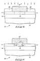
- second metal layer 18is formed into a structure 20 , and first metal layer 16 is outwardly exposed. Such is preferably conducted by subtractive patterning of metal layer 18 , for example by photolithographic patterning and etch.
- structure 20can be considered as comprising a metal mass projecting from underlying substrate material and having outer surfaces comprised of a top surface 22 and opposing side surfaces 24 which join with top surface 22 at respective angles. The preferred angles are preferably within about 15° of normal, with normal angles being shown in the figures.
- a chalcogenide material 26is formed over the substrate on second metal structure 20 outer surfaces 22 and 24 , and on exposed first metal layer 16 .
- Suchis preferably formed by blanket physical vapor deposition.
- a preferred deposition thickness for layer 26is preferably less than three times the thickness of deposited layer 18 , with an example being from about 525 Angstroms to about 900 Angstroms. More preferred is a thickness to provide layer 18 at 20% to 50% of layer 26 thickness.
- Exemplary preferred chalcogenide materialsinclude those disclosed in the Kozicki et al. patents referred to above.
- Specific preferred examplesinclude a chalcogenide material having metal ions diffused therein represented by the formula Ge x A y , where “A” is selected from the group consisting of Se, Te and S and mixtures thereof.
- Ais selected from the group consisting of Se, Te and S and mixtures thereof.
- the illustrated exampleprovides but one possible example of surrounding the exposed outer surfaces of a projecting metal mass with chalcogenide material in accordance with but one aspect of the invention.
- irradiatingis conducted through chalcogenide material 26 to patterned second metal 18 effective to break a chalcogenide bond of the chalcogenide material at an interface with the patterned second metal outer surfaces and the chalcogenide material, and to diffuse at least some of second metal 18 outwardly into the chalcogenide material.
- Metal doped material 27is formed thereby. Therefore as shown in the preferred embodiment, only a portion of blanket deposited chalcogenide material layer 26 is doped with second metal 18 .
- a preferred irradiatingincludes exposure to actinic radiation having a wavelength below 500 nanometers, with radiation exposure at between 404-408 nanometers being a more specific example.
- a specific example in a suitable UV radiation flood exposure toolis 4.5 mW/cm 2 , 15 minutes, 405 nm wavelength, at room ambient temperature and pressure.
- the irradiatingdiffuses only some of the metal from layer 18 outwardly into chalcogenide material, leaving a remnant structure 20 a . Accordingly, the projecting metal mass 20 a has a shape after the irradiating which is maintained in comparison to original shape 20 , but at a reduced size.
- FIG. 5illustrates a lesser preferred alternate embodiment 10 a whereby the irradiating and/or layer dimensions might be modified such that the irradiating diffuses all of projecting metal mass 20 outwardly into the chalcogenide material.
- the preferred exemplary tungsten material of layer 16does not appreciably diffuse into layer 26 .
- chalcogenide material 26 not doped with metal 18is substantially selectively etched from metal doped portion 27 of the chalcogenide material.
- substantially selectivemeans a relative etch ratio of layer 26 relative to layer 27 or at least 3:1.
- such etchingis preferably conducted to remove all of chalcogenide material 26 which has not been doped with metal 18 .
- the preferred etchingcomprises dry anisotropic etching, preferably dry plasma anisotropic etching.
- a principle preferred component of such etching gascomprises CF 4 .
- Top poweris preferably maintained at 500 watts, with the lower wafer susceptor being allowed to float.
- Susceptor temperatureis preferably maintained at about 25° C., and an exemplary reactor pressure is 50 mTorr.
- a specific example in a reactive ion etcheris CF 4 at 50 sccm, Ar at 25 sccm, susceptor temperature at 25° C., pressure of 50 mTorr and top power at 500 Watts.
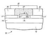
- an insulating layer 30has been deposited and metal doped chalcogenide material 27 has been exposed.
- An example and preferred material for layer 30is silicon nitride.
- an outer conductive electrode layer 32has been deposited and patterned to form the outer electrode of the preferred non-volatile resistance variable device.
- Example materialsinclude those disclosed in the above Kozicki et al. patents.
- silver structure 20 amight be designed and fabricated to constitute the effective quantity of silver for programming the device with no silver being provided in electrode 32 .
- layer 16might also constitute elemental silver with no silver being provided in electrode 32 .
- electrode 32might principally comprise elemental silver, or at least a lower silver portion in contact with the chalcogenide material 27 .
- the above-described preferred embodiment examplewas in conjunction with fabrication of a non-volatile resistance variable device.
- the inventionalso contemplates metal doping a chalcogenide material independent of the device being fabricated, and in the context of the accompanying claims as literally worded regarding methods of metal doping a chalcogenide material.
- the preferred exampleis with respect to formation of a projecting metal from an underlying substrate having chalcogenide material received thereover.
- the inventionis in no way so limited and also contemplates, by way of example only, diffusing metal from an entirely flat, or other, underlying surface into overlying chalcogenide material.
- the inventionalso contemplates non-volatile resistance variable devices independent of the method of manufacture.
- a deviceincludes a projecting metal mass (for example mass 20 a ) extending outwardly from a first metal layer laterally central into resistance variable chalcogenide material.
- the inventioncontemplates the device being in a highest resistance state for a given ambient temperature and pressure.
- the FIG. 8 device as depictedis in such a highest state of resistance.
- Progressively lower states of resistance for a given ambient temperature and pressurewill exist as a silver dendrite, in the preferred embodiment, progressively grows from an electrode to the point of contacting the opposing electrode.
- FIG. 8depicts but one exemplary embodiment of such a non-volatile resistance variable device having such a laterally central located projecting mass relative to material 27 .
- the inventionalso contemplates a non-volatile resistance variable device in a highest resistance state for a given ambient temperature and pressure independent of a conductive projection which is so centrally located.
- a non-volatile resistance variable devicein a highest resistance state for a given ambient temperature and pressure independent of a conductive projection which is so centrally located.
- Suchcomprises a resistance variable chalcogenide material having metal ions diffused therein.
- Opposing first and second electrodesare received operatively proximate the resistance variable, chalcogenide material, with at least one of the electrodes comprising a conductive projection extending into the resistance variable chalcogenide material. Provision of such a structure is in no way shown or suggested in a highest resistance state for a given ambient temperature and pressure in any of the teachings and drawings of the above-described Kozicki et al. patents.
Landscapes
- Engineering & Computer Science (AREA)
- Manufacturing & Machinery (AREA)
- Semiconductor Memories (AREA)
Abstract
Description
This application is a continuation of application Ser. No. 09/999,883, filed on Oct. 31, 2001, now U.S. Pat. No. 6,709,887, which in turn is a divisional of application Ser. No. 09/797,635, filed on Mar. 1, 2002, now U.S. Pat. No. 6,727,192, both of which applications are incorporated herein by reference.
This invention relates to non-volatile resistance variable devices and methods of forming the same.
Semiconductor fabrication continues to strive to make individual electronic components smaller and smaller, resulting in ever denser integrated circuitry. One type of integrated circuitry comprises memory circuitry where information is stored in the form of binary data. The circuitry can be fabricated such that the data is volatile or non-volatile. Volatile storing memory devices result in loss of data when power is interrupted. Non-volatile memory circuitry retains the stored data even when power is interrupted.
This invention was principally motivated in making improvements to the design and operation of memory circuitry disclosed in the Kozicki et al. U.S. Pat. Nos. 5,761,115; 5,896,312; 5,914,893; and 6,084,796, which ultimately resulted from U.S. patent application Ser. No. 08/652,706, filed on May 30, 1996, disclosing what is referred to as a programmable metalization cell. Such a cell includes opposing electrodes having an insulating dielectric material received therebetween. Received within the dielectric material is a fast ion conductor material. The resistance of such material can be changed between highly insulative and highly conductive states. In its normal high resistive state, to perform a write operation, a voltage potential is applied to a certain one of the electrodes, with the other of the electrode being held at zero voltage or ground. The electrode having the voltage applied thereto functions as an anode, while the electrode held at zero or ground functions as a cathode. The nature of the fast ion conductor material is such that it undergoes a chemical and structural change at a certain applied voltage. Specifically, at some suitable threshold voltage, plating of metal from metal ions within the material begins to occur on the cathode and grows or progresses through the fast ion conductor toward the other anode electrode. With such voltage continued to be applied, the process continues until a single conductive dendrite or filament extends between the electrodes, effectively interconnecting the top and bottom electrodes to electrically short them together.
Once this occurs, dendrite growth stops, and is retained when the voltage potentials are removed. Such can effectively result in the resistance of the mass of fast ion conductor material between electrodes dropping by a factor of 1,000. Such material can be returned to its highly resistive state by reversing the voltage potential between the anode and cathode, whereby the filament disappears. Again, the highly resistive state is maintained once the reverse voltage potentials are removed. Accordingly, such a device can, for example, function as a programmable memory cell of memory circuitry.
The preferred resistance variable material received between the electrodes typically and preferably comprises a chalcogenide material having metal ions diffused therein. A specific example is germanium selenide with silver ions. The present method of providing the silver ions within the germanium selenide material is to initially deposit the germanium selenide glass without any silver being received therein. A thin layer of silver is thereafter deposited upon the glass, for example by physical vapor deposition or other technique. An exemplary thickness is 200 Angstroms or less. The layer of silver is irradiated, preferably with electromagnetic energy at a wavelength less than 500 nanometers. The thin nature of the deposited silver enables such energy to pass through the silver to the silver/glass interface effective to break a chalcogenide bond of the chalcogenide material, thereby effecting dissolution of silver into the germanium selenide glass. The applied energy and overlying silver result in the silver migrating into the glass layer such that a homogenous distribution of silver throughout the layer is ultimately achieved.
It can be challenging to etch and to chemical-mechanical polish metal ion containing chalcogenide materials. Accordingly it would be desirable to develop memory cell fabrication methods which avoid one or both of etching or polishing such materials. It would also be desirable to develop alternate methods from that just described which incorporate the metal ions into chalcogenide materials. While the invention was principally motivated in achieving objectives such as these, the invention is in no way so limited. The artisan will appreciate applicability of the invention in other aspects of processing involving chalcogenide materials, with the invention only being limited by the accompanying claims as literally worded and as appropriately interpreted in accordance with the doctrine of equivalents.
The invention includes non-volatile resistance variable devices and methods of forming the same. In one implementation, a method of metal doping a chalcogenide material includes forming a metal over a substrate. A chalcogenide material is formed on the metal. Irradiating is conducted through the chalcogenide material to the metal effective to break a chalcogenide bond of the chalcogenide material at an interface of the metal and chalcogenide material and diffuse at least some of the metal outwardly into the chalcogenide material. In one implementation, a method of metal doping a chalcogenide material includes surrounding exposed outer surfaces of a projecting metal mass with chalcogenide material. Irradiating is conducted through the chalcogenide material to the projecting metal mass effective to break a chalcogenide bond of the chalcogenide material at an interface of the projecting metal mass outer surfaces and diffuse at least some of the projecting metal mass outwardly into the chalcogenide material. In certain aspects, the above implementations are incorporated in methods of forming non-volatile resistance variable devices.
In one implementation, a non-volatile resistance variable device in a highest resistance state for a given ambient temperature and pressure includes a resistance variable chalcogenide material having metal ions diffused therein. Opposing first and second electrodes are received operatively proximate the resistance variable chalcogenide material. At least one of the electrodes has a conductive projection extending into the resistance variable chalcogenide material.
Preferred embodiments of the invention are described below with reference to the following accompanying drawings.
This disclosure of the invention is submitted in furtherance of the constitutional purposes of the U.S. Patent Laws “to promote the progress of science and useful arts” (Article 1, Section 8).
Referring toFIG. 1 , asemiconductor wafer fragment 10 is shown in but one preferred embodiment of a method of forming a non-volatile resistance variable device. By way of example only, example such devices include programmable metalization cells and programmable optical elements of the patents referred to above, further by way of example only, including programmable capacitance elements, programmable resistance elements, programmable antifuses of integrated circuitry and programmable memory cells of memory circuitry. The above patents are herein incorporated by reference. The invention contemplates the fabrication techniques and structure of any existing non-volatile resistance variable device, as well as yet-to-be developed such devices. In the context of this document, the term “semiconductor substrate” or “semiconductive substrate” is defined to mean any construction comprising semiconductive material, including, but not limited to, bulk semiconductive materials such as a semiconductive wafer (either alone or in assemblies comprising other materials thereon), and semiconductive material layers (either alone or in assemblies comprising other materials). The term “substrate” refers to any supporting structure, including, but not limited to, the semiconductive substrates described above. Also in the context of this document, the term “layer” encompasses both the singular and the plural unless otherwise indicated. Further, it will be appreciated by the artisan that “resistance setable semiconductive material” and “resistance variable device” includes materials and devices wherein a property or properties in addition to resistance is/are also varied. For example, and by way of example only, the material's capacitance and/or inductance might also be changed in addition to resistance.
Asecond metal layer 18 is formed (preferably by a blanket deposition) onfirst metal layer 16. An exemplary preferred material in conjunction with the non-volatile resistance variable device being fabricated is elemental silver. A preferred thickness forlayer 18 is from about 175 Angstroms to about 300 Angstroms.
Referring toFIG. 2 ,second metal layer 18 is formed into astructure 20, andfirst metal layer 16 is outwardly exposed. Such is preferably conducted by subtractive patterning ofmetal layer 18, for example by photolithographic patterning and etch. In one implementation,structure 20 can be considered as comprising a metal mass projecting from underlying substrate material and having outer surfaces comprised of atop surface 22 and opposing side surfaces24 which join withtop surface 22 at respective angles. The preferred angles are preferably within about 15° of normal, with normal angles being shown in the figures.
Referring toFIG. 3 , achalcogenide material 26 is formed over the substrate onsecond metal structure 20outer surfaces first metal layer 16. Such is preferably formed by blanket physical vapor deposition. A preferred deposition thickness forlayer 26 is preferably less than three times the thickness of depositedlayer 18, with an example being from about 525 Angstroms to about 900 Angstroms. More preferred is a thickness to providelayer 18 at 20% to 50% oflayer 26 thickness. Exemplary preferred chalcogenide materials include those disclosed in the Kozicki et al. patents referred to above. Specific preferred examples include a chalcogenide material having metal ions diffused therein represented by the formula GexAy, where “A” is selected from the group consisting of Se, Te and S and mixtures thereof. The illustrated example provides but one possible example of surrounding the exposed outer surfaces of a projecting metal mass with chalcogenide material in accordance with but one aspect of the invention.
Referring toFIG. 4 , irradiating is conducted throughchalcogenide material 26 to patternedsecond metal 18 effective to break a chalcogenide bond of the chalcogenide material at an interface with the patterned second metal outer surfaces and the chalcogenide material, and to diffuse at least some ofsecond metal 18 outwardly into the chalcogenide material. Metal dopedmaterial 27 is formed thereby. Therefore as shown in the preferred embodiment, only a portion of blanket depositedchalcogenide material layer 26 is doped withsecond metal 18. A preferred irradiating includes exposure to actinic radiation having a wavelength below 500 nanometers, with radiation exposure at between 404-408 nanometers being a more specific example. A specific example in a suitable UV radiation flood exposure tool is 4.5 mW/cm2, 15 minutes, 405 nm wavelength, at room ambient temperature and pressure.
In the depicted and preferred embodiment, the irradiating diffuses only some of the metal fromlayer 18 outwardly into chalcogenide material, leaving aremnant structure 20a. Accordingly, the projectingmetal mass 20ahas a shape after the irradiating which is maintained in comparison tooriginal shape 20, but at a reduced size.FIG. 5 illustrates a lesser preferred alternate embodiment 10awhereby the irradiating and/or layer dimensions might be modified such that the irradiating diffuses all of projectingmetal mass 20 outwardly into the chalcogenide material.
The preferred exemplary tungsten material oflayer 16 does not appreciably diffuse intolayer 26. Referring to FIG.6 and regardless,chalcogenide material 26 not doped withmetal 18 is substantially selectively etched from metal dopedportion 27 of the chalcogenide material. In the context of this document, “substantially selective” means a relative etch ratio oflayer 26 relative to layer27 or at least 3:1. In the illustrated and preferred embodiment, such etching is preferably conducted to remove all ofchalcogenide material 26 which has not been doped withmetal 18. The preferred etching comprises dry anisotropic etching, preferably dry plasma anisotropic etching. A principle preferred component of such etching gas comprises CF4. Additional preferred gases in the chemistry include C2F6and C4F8. Top power is preferably maintained at 500 watts, with the lower wafer susceptor being allowed to float. Susceptor temperature is preferably maintained at about 25° C., and an exemplary reactor pressure is 50 mTorr. By way of example only, a specific example in a reactive ion etcher is CF4at 50 sccm, Ar at 25 sccm, susceptor temperature at 25° C., pressure of 50 mTorr and top power at 500 Watts.
Referring toFIG. 7 , an insulatinglayer 30 has been deposited and metal dopedchalcogenide material 27 has been exposed. An example and preferred material forlayer 30 is silicon nitride.
Referring toFIG. 8 , an outerconductive electrode layer 32 has been deposited and patterned to form the outer electrode of the preferred non-volatile resistance variable device. Example materials include those disclosed in the above Kozicki et al. patents. In the illustrated and described preferred example,silver structure 20amight be designed and fabricated to constitute the effective quantity of silver for programming the device with no silver being provided inelectrode 32. Alternately by way of example only,layer 16 might also constitute elemental silver with no silver being provided inelectrode 32. Further, by way of example only,electrode 32 might principally comprise elemental silver, or at least a lower silver portion in contact with thechalcogenide material 27.
The above-described preferred embodiment example was in conjunction with fabrication of a non-volatile resistance variable device. However, the invention also contemplates metal doping a chalcogenide material independent of the device being fabricated, and in the context of the accompanying claims as literally worded regarding methods of metal doping a chalcogenide material. Further, the preferred example is with respect to formation of a projecting metal from an underlying substrate having chalcogenide material received thereover. However, the invention is in no way so limited and also contemplates, by way of example only, diffusing metal from an entirely flat, or other, underlying surface into overlying chalcogenide material.
The invention also contemplates non-volatile resistance variable devices independent of the method of manufacture. In one implementation, such a device includes a projecting metal mass (forexample mass 20a) extending outwardly from a first metal layer laterally central into resistance variable chalcogenide material. In one aspect, the invention contemplates the device being in a highest resistance state for a given ambient temperature and pressure. For example, theFIG. 8 device as depicted is in such a highest state of resistance. Progressively lower states of resistance for a given ambient temperature and pressure will exist as a silver dendrite, in the preferred embodiment, progressively grows from an electrode to the point of contacting the opposing electrode.FIG. 8 depicts but one exemplary embodiment of such a non-volatile resistance variable device having such a laterally central located projecting mass relative tomaterial 27.
The invention also contemplates a non-volatile resistance variable device in a highest resistance state for a given ambient temperature and pressure independent of a conductive projection which is so centrally located. Such comprises a resistance variable chalcogenide material having metal ions diffused therein. Opposing first and second electrodes are received operatively proximate the resistance variable, chalcogenide material, with at least one of the electrodes comprising a conductive projection extending into the resistance variable chalcogenide material. Provision of such a structure is in no way shown or suggested in a highest resistance state for a given ambient temperature and pressure in any of the teachings and drawings of the above-described Kozicki et al. patents.
In compliance with the statute, the invention has been described in language more or less specific as to structural and methodical features. It is to be understood, however, that the invention is not limited to the specific features shown and described, since the means herein disclosed comprise preferred forms of putting the invention into effect. The invention is, therefore, claimed in any of its forms or modifications within the proper scope of the appended claims appropriately interpreted in accordance with the doctrine of equivalents.
Claims (26)
1. A method of forming a non-volatile resistance variable device comprising:
forming a substrate;
forming a projecting metal mass having an exposed outer surface on said substrate;
surrounding said exposed outer surface of said projecting metal mass with chalcogenide material;
diffusing a portion of said projecting metal mass outwardly into a portion of said chalcogenide material; and
forming an electrode over said chalcogenide material.
2. The method ofclaim 1 wherein the step of forming a projecting metal mass having an exposed outer surface further comprises the steps of:
forming a metal layer over said substrate; and
patterning said metal layer into a projecting metal mass having an exposed outer surface.
3. The method ofclaim 1 wherein said exposed outer surface of said projecting metal mass further comprises joining a top metal surface with opposing side metal surfaces at respective angles.
4. The method ofclaim 1 wherein said exposed outer surface of said projecting metal mass further comprises joining a top metal surface with opposing side metal surfaces at respective angles within about 15 degrees of normal.
5. The method ofclaim 1 wherein said portion of said projecting metal mass diffused outwardly into said chalcogenide material comprises less than all of said projecting metal mass.
6. The method ofclaim 5 wherein a portion of said projecting metal mass that is not diffused outwardly into said chalcogenide material is smaller but is substantially the same shape as said projecting metal mass before said portion of said projecting metal mass is diffused into said chalcogenide material.
7. The method ofclaim 1 wherein said portion of said projecting metal mass diffused outwardly into said chalcogenide material comprises all of said projecting metal mass.
8. The method ofclaim 1 wherein the step of surrounding said exposed outer surface of said projecting metal mass with chalcogenide material further comprises blanket deposition of chalcogenide material.
9. The method ofclaim 1 wherein the step of diffusing a portion of said projecting metal mass outwardly into said chalcogenide material further comprises irradiating through said chalcogenide material to said projecting metal mass.
10. The method ofclaim 9 wherein said step of irradiating further comprises irradiating through said chalcogenide material to said projecting metal mass with electromagnetic radiation having a wavelength less than about 500 nanometers.
11. The method ofclaim 10 wherein said electromagnetic radiation has a wavelength of about 404 nanometers to about 408 nanometers.
12. The method ofclaim 10 wherein said electromagnetic radiation has a wavelength of about 405 nanometers.
13. The method ofclaim 1 further comprising the step of substantially selectively etching a portion of said chalcogenide material into which a portion of projecting metal mass has not been diffused, before said step of forming an electrode over said chalcogenide material.
14. The method ofclaim 13 wherein said step of substantially selectively etching comprises dry anisotropic etching.
15. The method ofclaim 13 wherein said step of substantially selectively etching comprises dry anisotropic etching using a gas chemistry comprising CF4.
16. A method of forming a non-volatile resistance variable device comprising:
forming a first metal layer over a substrate;
forming a second metal layer on said first metal layer;
patterning said second metal layer into a structure having an outer surface and exposing said first metal layer;
blanket depositing a chalcogenide material over said substrate on said second metal structure outer surface and on said exposed first metal layer; and
diffusing a portion of said of said patterned second metal outwardly into a portion of said chalcogenide material.
17. The method ofclaim 16 further comprising the steps of:
substantially selectively etching a portion of said chalcogenide material into which a portion of said patterned second metal has not been diffused; and
after said step of substantially selectively etching, forming an outer electrode over a remaining portion of said chalcogenide material into which said portion of said patterned second metal has been diffused.
18. The method ofclaim 17 wherein said step of substantially selectively etching comprises dry anisotropic etching.
19. The method ofclaim 17 wherein said step of substantially selectively etching comprises dry anisotropic etching using a gas chemistry comprising CF4.
20. The method ofclaim 16 wherein said portion of said patterned second metal diffused outwardly into said chalcogenide material comprises less than all of said patterned second metal.
21. The method ofclaim 20 wherein a portion of said patterned second metal that is not diffused outwardly into said chalcogenide material is smaller but is substantially the same shape as said patterned second metal before said portion of said patterned second metal is diffused into said chalcogenide material.
22. The method ofclaim 16 wherein said portion of said patterned second metal diffused outwardly into said chalcogenide material comprises all of said patterned second metal.
23. The method ofclaim 16 wherein the step of diffusing a portion of said patterned second metal outwardly into said chalcogenide material further comprises irradiating through said chalcogenide material to said patterned second metal.
24. The method ofclaim 23 wherein said step of irradiating further comprises irradiating through said chalcogenide material to said patterned second metal with electromagnetic radiation having a wavelength less than about 500 nanometers.
25. The method ofclaim 24 wherein said electromagnetic radiation has a wavelength of about 404 nanometers to about 408 nanometers.
26. The method ofclaim 24 wherein said electromagnetic radiation has a wavelength of about 405 nanometers.
Priority Applications (1)
| Application Number | Priority Date | Filing Date | Title |
|---|---|---|---|
| US10/777,755US6949402B2 (en) | 2001-03-01 | 2004-02-13 | Method of forming a non-volatile resistance variable device |
Applications Claiming Priority (3)
| Application Number | Priority Date | Filing Date | Title |
|---|---|---|---|
| US09/797,635US6727192B2 (en) | 2001-03-01 | 2001-03-01 | Methods of metal doping a chalcogenide material |
| US09/999,883US6709887B2 (en) | 2001-03-01 | 2001-10-31 | Method of forming a chalcogenide comprising device |
| US10/777,755US6949402B2 (en) | 2001-03-01 | 2004-02-13 | Method of forming a non-volatile resistance variable device |
Related Parent Applications (1)
| Application Number | Title | Priority Date | Filing Date |
|---|---|---|---|
| US09/999,883ContinuationUS6709887B2 (en) | 2001-03-01 | 2001-10-31 | Method of forming a chalcogenide comprising device |
Publications (2)
| Publication Number | Publication Date |
|---|---|
| US20040161874A1 US20040161874A1 (en) | 2004-08-19 |
| US6949402B2true US6949402B2 (en) | 2005-09-27 |
Family
ID=25171391
Family Applications (6)
| Application Number | Title | Priority Date | Filing Date |
|---|---|---|---|
| US09/797,635Expired - LifetimeUS6727192B2 (en) | 2001-03-01 | 2001-03-01 | Methods of metal doping a chalcogenide material |
| US09/999,883Expired - LifetimeUS6709887B2 (en) | 2001-03-01 | 2001-10-31 | Method of forming a chalcogenide comprising device |
| US10/227,316Expired - LifetimeUS6710423B2 (en) | 2001-03-01 | 2002-08-23 | Chalcogenide comprising device |
| US10/774,515Expired - LifetimeUS7022555B2 (en) | 2001-03-01 | 2004-02-10 | Methods of forming a semiconductor memory device |
| US10/777,755Expired - LifetimeUS6949402B2 (en) | 2001-03-01 | 2004-02-13 | Method of forming a non-volatile resistance variable device |
| US11/219,742Expired - LifetimeUS7199444B2 (en) | 2001-03-01 | 2005-09-07 | Memory device, programmable resistance memory cell and memory array |
Family Applications Before (4)
| Application Number | Title | Priority Date | Filing Date |
|---|---|---|---|
| US09/797,635Expired - LifetimeUS6727192B2 (en) | 2001-03-01 | 2001-03-01 | Methods of metal doping a chalcogenide material |
| US09/999,883Expired - LifetimeUS6709887B2 (en) | 2001-03-01 | 2001-10-31 | Method of forming a chalcogenide comprising device |
| US10/227,316Expired - LifetimeUS6710423B2 (en) | 2001-03-01 | 2002-08-23 | Chalcogenide comprising device |
| US10/774,515Expired - LifetimeUS7022555B2 (en) | 2001-03-01 | 2004-02-10 | Methods of forming a semiconductor memory device |
Family Applications After (1)
| Application Number | Title | Priority Date | Filing Date |
|---|---|---|---|
| US11/219,742Expired - LifetimeUS7199444B2 (en) | 2001-03-01 | 2005-09-07 | Memory device, programmable resistance memory cell and memory array |
Country Status (1)
| Country | Link |
|---|---|
| US (6) | US6727192B2 (en) |
Cited By (2)
| Publication number | Priority date | Publication date | Assignee | Title |
|---|---|---|---|---|
| US20070241385A1 (en)* | 2006-04-14 | 2007-10-18 | Heon Yong Chang | Phase change memory device for optimized current consumption efficiency and operation speed and method of manufacturing the same |
| US20100032732A1 (en)* | 2008-08-06 | 2010-02-11 | International Business Machines Corporation | Electrical antifuse having a multi-thickness dielectric layer |
Families Citing this family (129)
| Publication number | Priority date | Publication date | Assignee | Title |
|---|---|---|---|---|
| US6653193B2 (en)* | 2000-12-08 | 2003-11-25 | Micron Technology, Inc. | Resistance variable device |
| US6638820B2 (en) | 2001-02-08 | 2003-10-28 | Micron Technology, Inc. | Method of forming chalcogenide comprising devices, method of precluding diffusion of a metal into adjacent chalcogenide material, and chalcogenide comprising devices |
| JP4742429B2 (en)* | 2001-02-19 | 2011-08-10 | 住友電気工業株式会社 | Method for producing glass particulate deposit |
| US6727192B2 (en) | 2001-03-01 | 2004-04-27 | Micron Technology, Inc. | Methods of metal doping a chalcogenide material |
| US6818481B2 (en) | 2001-03-07 | 2004-11-16 | Micron Technology, Inc. | Method to manufacture a buried electrode PCRAM cell |
| US6734455B2 (en) | 2001-03-15 | 2004-05-11 | Micron Technology, Inc. | Agglomeration elimination for metal sputter deposition of chalcogenides |
| US7102150B2 (en) | 2001-05-11 | 2006-09-05 | Harshfield Steven T | PCRAM memory cell and method of making same |
| US6951805B2 (en) | 2001-08-01 | 2005-10-04 | Micron Technology, Inc. | Method of forming integrated circuitry, method of forming memory circuitry, and method of forming random access memory circuitry |
| US6737312B2 (en) | 2001-08-27 | 2004-05-18 | Micron Technology, Inc. | Method of fabricating dual PCRAM cells sharing a common electrode |
| US6881623B2 (en) | 2001-08-29 | 2005-04-19 | Micron Technology, Inc. | Method of forming chalcogenide comprising devices, method of forming a programmable memory cell of memory circuitry, and a chalcogenide comprising device |
| US6784018B2 (en) | 2001-08-29 | 2004-08-31 | Micron Technology, Inc. | Method of forming chalcogenide comprising devices and method of forming a programmable memory cell of memory circuitry |
| US6955940B2 (en) | 2001-08-29 | 2005-10-18 | Micron Technology, Inc. | Method of forming chalcogenide comprising devices |
| US6646902B2 (en) | 2001-08-30 | 2003-11-11 | Micron Technology, Inc. | Method of retaining memory state in a programmable conductor RAM |
| US6709958B2 (en) | 2001-08-30 | 2004-03-23 | Micron Technology, Inc. | Integrated circuit device and fabrication using metal-doped chalcogenide materials |
| US7109056B2 (en)* | 2001-09-20 | 2006-09-19 | Micron Technology, Inc. | Electro-and electroless plating of metal in the manufacture of PCRAM devices |
| US6815818B2 (en) | 2001-11-19 | 2004-11-09 | Micron Technology, Inc. | Electrode structure for use in an integrated circuit |
| US6791859B2 (en) | 2001-11-20 | 2004-09-14 | Micron Technology, Inc. | Complementary bit PCRAM sense amplifier and method of operation |
| US6873538B2 (en) | 2001-12-20 | 2005-03-29 | Micron Technology, Inc. | Programmable conductor random access memory and a method for writing thereto |
| US6909656B2 (en) | 2002-01-04 | 2005-06-21 | Micron Technology, Inc. | PCRAM rewrite prevention |
| US20030143782A1 (en)* | 2002-01-31 | 2003-07-31 | Gilton Terry L. | Methods of forming germanium selenide comprising devices and methods of forming silver selenide comprising structures |
| US6867064B2 (en)* | 2002-02-15 | 2005-03-15 | Micron Technology, Inc. | Method to alter chalcogenide glass for improved switching characteristics |
| US6791885B2 (en) | 2002-02-19 | 2004-09-14 | Micron Technology, Inc. | Programmable conductor random access memory and method for sensing same |
| US6891749B2 (en) | 2002-02-20 | 2005-05-10 | Micron Technology, Inc. | Resistance variable ‘on ’ memory |
| US6847535B2 (en) | 2002-02-20 | 2005-01-25 | Micron Technology, Inc. | Removable programmable conductor memory card and associated read/write device and method of operation |
| US6809362B2 (en) | 2002-02-20 | 2004-10-26 | Micron Technology, Inc. | Multiple data state memory cell |
| US7087919B2 (en) | 2002-02-20 | 2006-08-08 | Micron Technology, Inc. | Layered resistance variable memory device and method of fabrication |
| US7151273B2 (en) | 2002-02-20 | 2006-12-19 | Micron Technology, Inc. | Silver-selenide/chalcogenide glass stack for resistance variable memory |
| US6937528B2 (en) | 2002-03-05 | 2005-08-30 | Micron Technology, Inc. | Variable resistance memory and method for sensing same |
| US6849868B2 (en) | 2002-03-14 | 2005-02-01 | Micron Technology, Inc. | Methods and apparatus for resistance variable material cells |
| US6751114B2 (en) | 2002-03-28 | 2004-06-15 | Micron Technology, Inc. | Method for programming a memory cell |
| US6855975B2 (en) | 2002-04-10 | 2005-02-15 | Micron Technology, Inc. | Thin film diode integrated with chalcogenide memory cell |
| US6858482B2 (en) | 2002-04-10 | 2005-02-22 | Micron Technology, Inc. | Method of manufacture of programmable switching circuits and memory cells employing a glass layer |
| US6864500B2 (en)* | 2002-04-10 | 2005-03-08 | Micron Technology, Inc. | Programmable conductor memory cell structure |
| US6731528B2 (en) | 2002-05-03 | 2004-05-04 | Micron Technology, Inc. | Dual write cycle programmable conductor memory system and method of operation |
| US6825135B2 (en) | 2002-06-06 | 2004-11-30 | Micron Technology, Inc. | Elimination of dendrite formation during metal/chalcogenide glass deposition |
| US6890790B2 (en)* | 2002-06-06 | 2005-05-10 | Micron Technology, Inc. | Co-sputter deposition of metal-doped chalcogenides |
| US7209378B2 (en) | 2002-08-08 | 2007-04-24 | Micron Technology, Inc. | Columnar 1T-N memory cell structure |
| US7018863B2 (en) | 2002-08-22 | 2006-03-28 | Micron Technology, Inc. | Method of manufacture of a resistance variable memory cell |
| US7364644B2 (en)* | 2002-08-29 | 2008-04-29 | Micron Technology, Inc. | Silver selenide film stoichiometry and morphology control in sputter deposition |
| US7010644B2 (en) | 2002-08-29 | 2006-03-07 | Micron Technology, Inc. | Software refreshed memory device and method |
| US7294527B2 (en) | 2002-08-29 | 2007-11-13 | Micron Technology Inc. | Method of forming a memory cell |
| US6867114B2 (en) | 2002-08-29 | 2005-03-15 | Micron Technology Inc. | Methods to form a memory cell with metal-rich metal chalcogenide |
| US6831019B1 (en) | 2002-08-29 | 2004-12-14 | Micron Technology, Inc. | Plasma etching methods and methods of forming memory devices comprising a chalcogenide comprising layer received operably proximate conductive electrodes |
| US20040040837A1 (en)* | 2002-08-29 | 2004-03-04 | Mcteer Allen | Method of forming chalcogenide sputter target |
| US6867996B2 (en)* | 2002-08-29 | 2005-03-15 | Micron Technology, Inc. | Single-polarity programmable resistance-variable memory element |
| US6864521B2 (en) | 2002-08-29 | 2005-03-08 | Micron Technology, Inc. | Method to control silver concentration in a resistance variable memory element |
| US7163837B2 (en) | 2002-08-29 | 2007-01-16 | Micron Technology, Inc. | Method of forming a resistance variable memory element |
| US6903394B2 (en)* | 2002-11-27 | 2005-06-07 | Micron Technology, Inc. | CMOS imager with improved color response |
| US7337160B2 (en)* | 2002-12-31 | 2008-02-26 | Bae Systems Information And Electronic Systems Integration Inc. | Use of radiation-hardened chalcogenide technology for spaceborne reconfigurable digital processing systems |
| US6813178B2 (en)* | 2003-03-12 | 2004-11-02 | Micron Technology, Inc. | Chalcogenide glass constant current device, and its method of fabrication and operation |
| US7022579B2 (en) | 2003-03-14 | 2006-04-04 | Micron Technology, Inc. | Method for filling via with metal |
| US7050327B2 (en) | 2003-04-10 | 2006-05-23 | Micron Technology, Inc. | Differential negative resistance memory |
| US7067865B2 (en)* | 2003-06-06 | 2006-06-27 | Macronix International Co., Ltd. | High density chalcogenide memory cells |
| US6930909B2 (en) | 2003-06-25 | 2005-08-16 | Micron Technology, Inc. | Memory device and methods of controlling resistance variation and resistance profile drift |
| US6961277B2 (en) | 2003-07-08 | 2005-11-01 | Micron Technology, Inc. | Method of refreshing a PCRAM memory device |
| US7061004B2 (en) | 2003-07-21 | 2006-06-13 | Micron Technology, Inc. | Resistance variable memory elements and methods of formation |
| US6903361B2 (en) | 2003-09-17 | 2005-06-07 | Micron Technology, Inc. | Non-volatile memory structure |
| US7858980B2 (en)* | 2004-03-01 | 2010-12-28 | Taiwan Semiconductor Manufacturing Co., Ltd. | Reduced active area in a phase change memory structure |
| US7098068B2 (en) | 2004-03-10 | 2006-08-29 | Micron Technology, Inc. | Method of forming a chalcogenide material containing device |
| US7583551B2 (en) | 2004-03-10 | 2009-09-01 | Micron Technology, Inc. | Power management control and controlling memory refresh operations |
| DE102004014965B4 (en)* | 2004-03-26 | 2007-12-27 | Qimonda Ag | Method for producing a nonvolatile memory cell |
| US7145795B2 (en)* | 2004-04-13 | 2006-12-05 | Micron Technology, Inc. | Multi-cell resistive memory array architecture with select transistor |
| CN1977513B (en)* | 2004-06-29 | 2010-09-01 | 皇家飞利浦电子股份有限公司 | System and methods for efficient authentication of medical wireless self-organizing network nodes |
| KR100668824B1 (en)* | 2004-06-30 | 2007-01-16 | 주식회사 하이닉스반도체 | Phase change memory device and its manufacturing method |
| US7326950B2 (en) | 2004-07-19 | 2008-02-05 | Micron Technology, Inc. | Memory device with switching glass layer |
| US7354793B2 (en) | 2004-08-12 | 2008-04-08 | Micron Technology, Inc. | Method of forming a PCRAM device incorporating a resistance-variable chalocogenide element |
| US7190048B2 (en) | 2004-07-19 | 2007-03-13 | Micron Technology, Inc. | Resistance variable memory device and method of fabrication |
| US7226857B2 (en)* | 2004-07-30 | 2007-06-05 | Micron Technology, Inc. | Front-end processing of nickel plated bond pads |
| US7365411B2 (en) | 2004-08-12 | 2008-04-29 | Micron Technology, Inc. | Resistance variable memory with temperature tolerant materials |
| US7151688B2 (en) | 2004-09-01 | 2006-12-19 | Micron Technology, Inc. | Sensing of resistance variable memory devices |
| US7224598B2 (en)* | 2004-09-02 | 2007-05-29 | Hewlett-Packard Development Company, L.P. | Programming of programmable resistive memory devices |
| DE102004052648A1 (en)* | 2004-10-29 | 2006-05-04 | Infineon Technologies Ag | Non-volatile (sic) resistive storage cell with solid electrolyte matrix (300) between first (1) and second (2) electrode as active layer useful in semiconductor technology has elements from groups IVb and Vb |
| US7106096B2 (en)* | 2004-11-11 | 2006-09-12 | International Business Machines Corporation | Circuit and method of controlling integrated circuit power consumption using phase change switches |
| US7138290B2 (en)* | 2004-12-03 | 2006-11-21 | Micron Technology, Inc. | Methods of depositing silver onto a metal selenide-comprising surface and methods of depositing silver onto a selenium-comprising surface |
| US6972429B1 (en)* | 2004-12-16 | 2005-12-06 | Macronix International Co, Ltd. | Chalcogenide random access memory and method of fabricating the same |
| US20060131555A1 (en)* | 2004-12-22 | 2006-06-22 | Micron Technology, Inc. | Resistance variable devices with controllable channels |
| US7374174B2 (en) | 2004-12-22 | 2008-05-20 | Micron Technology, Inc. | Small electrode for resistance variable devices |
| US20060172067A1 (en)* | 2005-01-28 | 2006-08-03 | Energy Conversion Devices, Inc | Chemical vapor deposition of chalcogenide materials |
| US7317200B2 (en) | 2005-02-23 | 2008-01-08 | Micron Technology, Inc. | SnSe-based limited reprogrammable cell |
| US7749805B2 (en)* | 2005-03-10 | 2010-07-06 | Qimonda Ag | Method for manufacturing an integrated circuit including an electrolyte material layer |
| DE102005012047A1 (en)* | 2005-03-16 | 2006-09-28 | Infineon Technologies Ag | Solid-state electrolyte memory manufacture involves coating first electrode with solid-state electrolyte layer, and then forming second electrode on solid-state electrolyte layer |
| US7427770B2 (en) | 2005-04-22 | 2008-09-23 | Micron Technology, Inc. | Memory array for increased bit density |
| US7269044B2 (en) | 2005-04-22 | 2007-09-11 | Micron Technology, Inc. | Method and apparatus for accessing a memory array |
| US7709289B2 (en) | 2005-04-22 | 2010-05-04 | Micron Technology, Inc. | Memory elements having patterned electrodes and method of forming the same |
| US7269079B2 (en) | 2005-05-16 | 2007-09-11 | Micron Technology, Inc. | Power circuits for reducing a number of power supply voltage taps required for sensing a resistive memory |
| JP4285452B2 (en)* | 2005-07-06 | 2009-06-24 | 株式会社日立製作所 | Device and manufacturing method thereof |
| US7233520B2 (en) | 2005-07-08 | 2007-06-19 | Micron Technology, Inc. | Process for erasing chalcogenide variable resistance memory bits |
| US7274034B2 (en) | 2005-08-01 | 2007-09-25 | Micron Technology, Inc. | Resistance variable memory device with sputtered metal-chalcogenide region and method of fabrication |
| US7332735B2 (en) | 2005-08-02 | 2008-02-19 | Micron Technology, Inc. | Phase change memory cell and method of formation |
| US7317567B2 (en) | 2005-08-02 | 2008-01-08 | Micron Technology, Inc. | Method and apparatus for providing color changing thin film material |
| US20070037316A1 (en)* | 2005-08-09 | 2007-02-15 | Micron Technology, Inc. | Memory cell contact using spacers |
| US7579615B2 (en) | 2005-08-09 | 2009-08-25 | Micron Technology, Inc. | Access transistor for memory device |
| US7304368B2 (en) | 2005-08-11 | 2007-12-04 | Micron Technology, Inc. | Chalcogenide-based electrokinetic memory element and method of forming the same |
| US7251154B2 (en) | 2005-08-15 | 2007-07-31 | Micron Technology, Inc. | Method and apparatus providing a cross-point memory array using a variable resistance memory cell and capacitance |
| US7277313B2 (en) | 2005-08-31 | 2007-10-02 | Micron Technology, Inc. | Resistance variable memory element with threshold device and method of forming the same |
| US8062833B2 (en)* | 2005-12-30 | 2011-11-22 | Macronix International Co., Ltd. | Chalcogenide layer etching method |
| US7560337B2 (en)* | 2006-01-09 | 2009-07-14 | Macronix International Co., Ltd. | Programmable resistive RAM and manufacturing method |
| TWI299527B (en)* | 2006-04-11 | 2008-08-01 | Taiwan Tft Lcd Ass | A fabrication method of thin film for active layer by metal chalcogenide precursor solution |
| US7785920B2 (en)* | 2006-07-12 | 2010-08-31 | Macronix International Co., Ltd. | Method for making a pillar-type phase change memory element |
| US7560723B2 (en) | 2006-08-29 | 2009-07-14 | Micron Technology, Inc. | Enhanced memory density resistance variable memory cells, arrays, devices and systems including the same, and methods of fabrication |
| KR100850482B1 (en) | 2007-03-29 | 2008-08-05 | 한양대학교 산학협력단 | Method for manufacturing conductive polymer nanostructures and nanostructures prepared thereby |
| US7989793B2 (en)* | 2007-12-10 | 2011-08-02 | Electronics And Telecommunications Research Institute | Electrical device using phase change material, phase change memory device using solid state reaction and method for fabricating the same |
| US7879643B2 (en)* | 2008-01-18 | 2011-02-01 | Macronix International Co., Ltd. | Memory cell with memory element contacting an inverted T-shaped bottom electrode |
| US7879645B2 (en)* | 2008-01-28 | 2011-02-01 | Macronix International Co., Ltd. | Fill-in etching free pore device |
| US8467236B2 (en) | 2008-08-01 | 2013-06-18 | Boise State University | Continuously variable resistor |
| US8063394B2 (en)* | 2008-10-08 | 2011-11-22 | Qimonda Ag | Integrated circuit |
| WO2010077622A1 (en)* | 2008-12-08 | 2010-07-08 | Arizona Board Of Regents, Acting For And On Behalf Of Arizona State University | Electrical devices including dendritic metal electrodes |
| US7839681B2 (en)* | 2008-12-12 | 2010-11-23 | Actel Corporation | Push-pull FPGA cell |
| US7929345B2 (en)* | 2008-12-23 | 2011-04-19 | Actel Corporation | Push-pull memory cell configured for simultaneous programming of n-channel and p-channel non-volatile transistors |
| US8120955B2 (en)* | 2009-02-13 | 2012-02-21 | Actel Corporation | Array and control method for flash based FPGA cell |
| US8269204B2 (en) | 2009-07-02 | 2012-09-18 | Actel Corporation | Back to back resistive random access memory cells |
| US8279665B2 (en)* | 2009-11-23 | 2012-10-02 | International Business Machines Corporation | Memory cell and select element |
| US8134139B2 (en)* | 2010-01-25 | 2012-03-13 | Macronix International Co., Ltd. | Programmable metallization cell with ion buffer layer |
| US8962460B2 (en) | 2011-04-26 | 2015-02-24 | Micron Technology, Inc. | Methods of selectively forming metal-doped chalcogenide materials, methods of selectively doping chalcogenide materials, and methods of forming semiconductor device structures including same |
| US8921818B2 (en)* | 2012-11-09 | 2014-12-30 | Taiwan Semiconductor Manufacturing Company, Ltd. | Resistance variable memory structure |
| US9837605B2 (en)* | 2013-08-16 | 2017-12-05 | Taiwan Semiconductor Manufacturing Company, Ltd. | Memory cell having resistance variable film and method of making the same |
| US9245742B2 (en) | 2013-12-18 | 2016-01-26 | Asm Ip Holding B.V. | Sulfur-containing thin films |
| US9478419B2 (en) | 2013-12-18 | 2016-10-25 | Asm Ip Holding B.V. | Sulfur-containing thin films |
| US9461134B1 (en) | 2015-05-20 | 2016-10-04 | Asm Ip Holding B.V. | Method for forming source/drain contact structure with chalcogen passivation |
| US9711350B2 (en) | 2015-06-03 | 2017-07-18 | Asm Ip Holding B.V. | Methods for semiconductor passivation by nitridation |
| US10490475B2 (en) | 2015-06-03 | 2019-11-26 | Asm Ip Holding B.V. | Methods for semiconductor passivation by nitridation after oxide removal |
| US9741815B2 (en) | 2015-06-16 | 2017-08-22 | Asm Ip Holding B.V. | Metal selenide and metal telluride thin films for semiconductor device applications |
| US9711396B2 (en) | 2015-06-16 | 2017-07-18 | Asm Ip Holding B.V. | Method for forming metal chalcogenide thin films on a semiconductor device |
| US10270451B2 (en) | 2015-12-17 | 2019-04-23 | Microsemi SoC Corporation | Low leakage ReRAM FPGA configuration cell |
| US10256406B2 (en) | 2016-05-16 | 2019-04-09 | Micron Technology, Inc. | Semiconductor structures including liners and related methods |
| US10147485B2 (en) | 2016-09-29 | 2018-12-04 | Microsemi Soc Corp. | Circuits and methods for preventing over-programming of ReRAM-based memory cells |
| WO2018106450A1 (en) | 2016-12-09 | 2018-06-14 | Microsemi Soc Corp. | Resistive random access memory cell |
| US10522224B2 (en) | 2017-08-11 | 2019-12-31 | Microsemi Soc Corp. | Circuitry and methods for programming resistive random access memory devices |
| KR102109347B1 (en) | 2018-11-14 | 2020-05-12 | 성균관대학교산학협력단 | Preparing method of doped metal-chalcogenide thin film |
Citations (158)
| Publication number | Priority date | Publication date | Assignee | Title |
|---|---|---|---|---|
| US3271591A (en) | 1963-09-20 | 1966-09-06 | Energy Conversion Devices Inc | Symmetrical current controlling device |
| US3622319A (en) | 1966-10-20 | 1971-11-23 | Western Electric Co | Nonreflecting photomasks and methods of making same |
| US3743847A (en) | 1971-06-01 | 1973-07-03 | Motorola Inc | Amorphous silicon film as a uv filter |
| US3961314A (en) | 1974-03-05 | 1976-06-01 | Energy Conversion Devices, Inc. | Structure and method for producing an image |
| US3966317A (en) | 1974-04-08 | 1976-06-29 | Energy Conversion Devices, Inc. | Dry process production of archival microform records from hard copy |
| US3983542A (en) | 1970-08-13 | 1976-09-28 | Energy Conversion Devices, Inc. | Method and apparatus for recording information |
| US4158133A (en)* | 1976-08-20 | 1979-06-12 | Siemens Aktiengesellschaft | Filters for photo-detectors |
| US4177474A (en) | 1977-05-18 | 1979-12-04 | Energy Conversion Devices, Inc. | High temperature amorphous semiconductor member and method of making the same |
| US4267261A (en) | 1971-07-15 | 1981-05-12 | Energy Conversion Devices, Inc. | Method for full format imaging |
| US4269935A (en) | 1979-07-13 | 1981-05-26 | Ionomet Company, Inc. | Process of doping silver image in chalcogenide layer |
| JPS56126915A (en) | 1980-03-11 | 1981-10-05 | Fujitsu Ltd | Manufacture of semiconductor device |
| US4312938A (en) | 1979-07-06 | 1982-01-26 | Drexler Technology Corporation | Method for making a broadband reflective laser recording and data storage medium with absorptive underlayer |
| US4316946A (en) | 1979-12-03 | 1982-02-23 | Ionomet Company, Inc. | Surface sensitized chalcogenide product and process for making and using the same |
| US4320191A (en) | 1978-11-07 | 1982-03-16 | Nippon Telegraph & Telephone Public Corporation | Pattern-forming process |
| US4405710A (en) | 1981-06-22 | 1983-09-20 | Cornell Research Foundation, Inc. | Ion beam exposure of (g-Gex -Se1-x) inorganic resists |
| US4419421A (en) | 1979-01-15 | 1983-12-06 | Max-Planck-Gesellschaft Zur Forderung Der Wissenschaften E.V. | Ion conductor material |
| US4499557A (en) | 1980-10-28 | 1985-02-12 | Energy Conversion Devices, Inc. | Programmable cell for use in programmable electronic arrays |
| US4597162A (en) | 1983-01-18 | 1986-07-01 | Energy Conversion Devices, Inc. | Method for making, parallel preprogramming or field programming of electronic matrix arrays |
| US4608296A (en) | 1983-12-06 | 1986-08-26 | Energy Conversion Devices, Inc. | Superconducting films and devices exhibiting AC to DC conversion |
| US4637895A (en) | 1985-04-01 | 1987-01-20 | Energy Conversion Devices, Inc. | Gas mixtures for the vapor deposition of semiconductor material |
| US4646266A (en) | 1984-09-28 | 1987-02-24 | Energy Conversion Devices, Inc. | Programmable semiconductor structures and methods for using the same |
| US4664939A (en) | 1985-04-01 | 1987-05-12 | Energy Conversion Devices, Inc. | Vertical semiconductor processor |
| US4668968A (en) | 1984-05-14 | 1987-05-26 | Energy Conversion Devices, Inc. | Integrated circuit compatible thin film field effect transistor and method of making same |
| US4670763A (en) | 1984-05-14 | 1987-06-02 | Energy Conversion Devices, Inc. | Thin film field effect transistor |
| US4671618A (en) | 1986-05-22 | 1987-06-09 | Wu Bao Gang | Liquid crystalline-plastic material having submillisecond switch times and extended memory |
| US4673957A (en) | 1984-05-14 | 1987-06-16 | Energy Conversion Devices, Inc. | Integrated circuit compatible thin film field effect transistor and method of making same |
| US4678679A (en) | 1984-06-25 | 1987-07-07 | Energy Conversion Devices, Inc. | Continuous deposition of activated process gases |
| US4710899A (en) | 1985-06-10 | 1987-12-01 | Energy Conversion Devices, Inc. | Data storage medium incorporating a transition metal for increased switching speed |
| US4728406A (en) | 1986-08-18 | 1988-03-01 | Energy Conversion Devices, Inc. | Method for plasma - coating a semiconductor body |
| US4737379A (en) | 1982-09-24 | 1988-04-12 | Energy Conversion Devices, Inc. | Plasma deposited coatings, and low temperature plasma method of making same |
| US4766471A (en) | 1986-01-23 | 1988-08-23 | Energy Conversion Devices, Inc. | Thin film electro-optical devices |
| US4769338A (en) | 1984-05-14 | 1988-09-06 | Energy Conversion Devices, Inc. | Thin film field effect transistor and method of making same |
| US4775425A (en) | 1987-07-27 | 1988-10-04 | Energy Conversion Devices, Inc. | P and n-type microcrystalline semiconductor alloy material including band gap widening elements, devices utilizing same |
| US4788594A (en) | 1986-10-15 | 1988-11-29 | Energy Conversion Devices, Inc. | Solid state electronic camera including thin film matrix of photosensors |
| US4795657A (en) | 1984-04-13 | 1989-01-03 | Energy Conversion Devices, Inc. | Method of fabricating a programmable array |
| US4800526A (en) | 1987-05-08 | 1989-01-24 | Gaf Corporation | Memory element for information storage and retrieval system and associated process |
| US4809044A (en) | 1986-08-22 | 1989-02-28 | Energy Conversion Devices, Inc. | Thin film overvoltage protection devices |
| US4818717A (en) | 1986-06-27 | 1989-04-04 | Energy Conversion Devices, Inc. | Method for making electronic matrix arrays |
| US4843443A (en) | 1984-05-14 | 1989-06-27 | Energy Conversion Devices, Inc. | Thin film field effect transistor and method of making same |
| US4845533A (en) | 1986-08-22 | 1989-07-04 | Energy Conversion Devices, Inc. | Thin film electrical devices with amorphous carbon electrodes and method of making same |
| US4847674A (en) | 1987-03-10 | 1989-07-11 | Advanced Micro Devices, Inc. | High speed interconnect system with refractory non-dogbone contacts and an active electromigration suppression mechanism |
| US4853785A (en) | 1986-10-15 | 1989-08-01 | Energy Conversion Devices, Inc. | Electronic camera including electronic signal storage cartridge |
| US4891330A (en) | 1987-07-27 | 1990-01-02 | Energy Conversion Devices, Inc. | Method of fabricating n-type and p-type microcrystalline semiconductor alloy material including band gap widening elements |
| US5128099A (en) | 1991-02-15 | 1992-07-07 | Energy Conversion Devices, Inc. | Congruent state changeable optical memory material and device |
| US5159661A (en) | 1990-10-05 | 1992-10-27 | Energy Conversion Devices, Inc. | Vertically interconnected parallel distributed processor |
| US5166758A (en) | 1991-01-18 | 1992-11-24 | Energy Conversion Devices, Inc. | Electrically erasable phase change memory |
| US5177567A (en) | 1991-07-19 | 1993-01-05 | Energy Conversion Devices, Inc. | Thin-film structure for chalcogenide electrical switching devices and process therefor |
| US5219788A (en) | 1991-02-25 | 1993-06-15 | Ibm Corporation | Bilayer metallization cap for photolithography |
| US5238862A (en) | 1992-03-18 | 1993-08-24 | Micron Technology, Inc. | Method of forming a stacked capacitor with striated electrode |
| US5272359A (en) | 1988-04-07 | 1993-12-21 | California Institute Of Technology | Reversible non-volatile switch based on a TCNQ charge transfer complex |
| US5296716A (en) | 1991-01-18 | 1994-03-22 | Energy Conversion Devices, Inc. | Electrically erasable, directly overwritable, multibit single cell memory elements and arrays fabricated therefrom |
| US5314772A (en) | 1990-10-09 | 1994-05-24 | Arizona Board Of Regents | High resolution, multi-layer resist for microlithography and method therefor |
| US5315131A (en) | 1990-11-22 | 1994-05-24 | Matsushita Electric Industrial Co., Ltd. | Electrically reprogrammable nonvolatile memory device |
| US5335219A (en) | 1991-01-18 | 1994-08-02 | Ovshinsky Stanford R | Homogeneous composition of microcrystalline semiconductor material, semiconductor devices and directly overwritable memory elements fabricated therefrom, and arrays fabricated from the memory elements |
| US5341328A (en) | 1991-01-18 | 1994-08-23 | Energy Conversion Devices, Inc. | Electrically erasable memory elements having reduced switching current requirements and increased write/erase cycle life |
| US5350484A (en) | 1992-09-08 | 1994-09-27 | Intel Corporation | Method for the anisotropic etching of metal films in the fabrication of interconnects |
| US5359205A (en) | 1991-11-07 | 1994-10-25 | Energy Conversion Devices, Inc. | Electrically erasable memory elements characterized by reduced current and improved thermal stability |
| US5360981A (en) | 1989-05-11 | 1994-11-01 | British Telecommunications Public Limited Company | Amorphous silicon memory |
| US5406509A (en) | 1991-01-18 | 1995-04-11 | Energy Conversion Devices, Inc. | Electrically erasable, directly overwritable, multibit single cell memory elements and arrays fabricated therefrom |
| US5414271A (en) | 1991-01-18 | 1995-05-09 | Energy Conversion Devices, Inc. | Electrically erasable memory elements having improved set resistance stability |
| US5500532A (en) | 1994-08-18 | 1996-03-19 | Arizona Board Of Regents | Personal electronic dosimeter |
| US5512773A (en) | 1993-12-23 | 1996-04-30 | U.S. Philips Corporation | Switching element with memory provided with Schottky tunnelling barrier |
| US5512328A (en) | 1992-08-07 | 1996-04-30 | Hitachi, Ltd. | Method for forming a pattern and forming a thin film used in pattern formation |
| US5534712A (en) | 1991-01-18 | 1996-07-09 | Energy Conversion Devices, Inc. | Electrically erasable memory elements characterized by reduced current and improved thermal stability |
| US5534711A (en) | 1991-01-18 | 1996-07-09 | Energy Conversion Devices, Inc. | Electrically erasable, directly overwritable, multibit single cell memory elements and arrays fabricated therefrom |
| US5536947A (en) | 1991-01-18 | 1996-07-16 | Energy Conversion Devices, Inc. | Electrically erasable, directly overwritable, multibit single cell memory element and arrays fabricated therefrom |
| US5543737A (en) | 1995-02-10 | 1996-08-06 | Energy Conversion Devices, Inc. | Logical operation circuit employing two-terminal chalcogenide switches |
| US5591501A (en) | 1995-12-20 | 1997-01-07 | Energy Conversion Devices, Inc. | Optical recording medium having a plurality of discrete phase change data recording points |
| US5596522A (en) | 1991-01-18 | 1997-01-21 | Energy Conversion Devices, Inc. | Homogeneous compositions of microcrystalline semiconductor material, semiconductor devices and directly overwritable memory elements fabricated therefrom, and arrays fabricated from the memory elements |
| US5687112A (en) | 1996-04-19 | 1997-11-11 | Energy Conversion Devices, Inc. | Multibit single cell memory element having tapered contact |
| US5694054A (en) | 1995-11-28 | 1997-12-02 | Energy Conversion Devices, Inc. | Integrated drivers for flat panel displays employing chalcogenide logic elements |
| WO1997048032A2 (en) | 1996-05-30 | 1997-12-18 | Axon Technologies Corporation | Programmable metallization cell and method of making |
| US5714768A (en) | 1995-10-24 | 1998-02-03 | Energy Conversion Devices, Inc. | Second-layer phase change memory array on top of a logic device |
| US5726083A (en) | 1994-11-29 | 1998-03-10 | Nec Corporation | Process of fabricating dynamic random access memory device having storage capacitor low in contact resistance and small in leakage current through tantalum oxide film |
| US5751012A (en) | 1995-06-07 | 1998-05-12 | Micron Technology, Inc. | Polysilicon pillar diode for use in a non-volatile memory cell |
| US5789277A (en) | 1996-07-22 | 1998-08-04 | Micron Technology, Inc. | Method of making chalogenide memory device |
| US5825046A (en) | 1996-10-28 | 1998-10-20 | Energy Conversion Devices, Inc. | Composite memory material comprising a mixture of phase-change memory material and dielectric material |
| US5841150A (en) | 1995-06-07 | 1998-11-24 | Micron Technology, Inc. | Stack/trench diode for use with a muti-state material in a non-volatile memory cell |
| US5846889A (en) | 1997-03-14 | 1998-12-08 | The United States Of America As Represented By The Secretary Of The Navy | Infrared transparent selenide glasses |
| US5912839A (en) | 1998-06-23 | 1999-06-15 | Energy Conversion Devices, Inc. | Universal memory element and method of programming same |
| US5914993A (en) | 1995-03-08 | 1999-06-22 | U.S. Philips Corporation | Multirate transmission system |
| US5920788A (en) | 1995-06-07 | 1999-07-06 | Micron Technology, Inc. | Chalcogenide memory cell with a plurality of chalcogenide electrodes |
| US5933365A (en) | 1997-06-19 | 1999-08-03 | Energy Conversion Devices, Inc. | Memory element with energy control mechanism |
| WO1999028914A3 (en) | 1997-12-04 | 1999-08-26 | Axon Technologies Corp | Programmable sub-surface aggregating metallization structure and method of making same |
| US5998066A (en) | 1997-05-16 | 1999-12-07 | Aerial Imaging Corporation | Gray scale mask and depth pattern transfer technique using inorganic chalcogenide glass |
| US6011757A (en) | 1998-01-27 | 2000-01-04 | Ovshinsky; Stanford R. | Optical recording media having increased erasability |
| US6072716A (en) | 1999-04-14 | 2000-06-06 | Massachusetts Institute Of Technology | Memory structures and methods of making same |
| US6077729A (en) | 1995-06-07 | 2000-06-20 | Micron Technology, Inc. | Memory array having a multi-state element and method for forming such array or cellis thereof |
| US6087674A (en) | 1996-10-28 | 2000-07-11 | Energy Conversion Devices, Inc. | Memory element with memory material comprising phase-change material and dielectric material |
| WO2000048196A1 (en) | 1999-02-11 | 2000-08-17 | Arizona Board Of Regents | Programmable microelectronic devices and methods of forming and programming same |
| US6117720A (en) | 1995-06-07 | 2000-09-12 | Micron Technology, Inc. | Method of making an integrated circuit electrode having a reduced contact area |
| US6141241A (en) | 1998-06-23 | 2000-10-31 | Energy Conversion Devices, Inc. | Universal memory element with systems employing same and apparatus and method for reading, writing and programming same |
| US6143604A (en) | 1999-06-04 | 2000-11-07 | Taiwan Semiconductor Manufacturing Company | Method for fabricating small-size two-step contacts for word-line strapping on dynamic random access memory (DRAM) |
| US6177338B1 (en) | 1999-02-08 | 2001-01-23 | Taiwan Semiconductor Manufacturing Company | Two step barrier process |
| US6236059B1 (en) | 1996-08-22 | 2001-05-22 | Micron Technology, Inc. | Memory cell incorporating a chalcogenide element and method of making same |
| US6297170B1 (en) | 1998-06-23 | 2001-10-02 | Vlsi Technology, Inc. | Sacrificial multilayer anti-reflective coating for mos gate formation |
| US6300684B1 (en) | 1995-06-07 | 2001-10-09 | Micron Technology, Inc. | Method for fabricating an array of ultra-small pores for chalcogenide memory cells |
| US6329606B1 (en) | 1996-04-24 | 2001-12-11 | Amkor Technology, Inc. | Grid array assembly of circuit boards with singulation grooves |
| US20020000666A1 (en) | 1998-08-31 | 2002-01-03 | Michael N. Kozicki | Self-repairing interconnections for electrical circuits |
| US6339544B1 (en) | 2000-09-29 | 2002-01-15 | Intel Corporation | Method to enhance performance of thermal resistor device |
| US6348365B1 (en) | 2001-03-02 | 2002-02-19 | Micron Technology, Inc. | PCRAM cell manufacturing |
| US6350679B1 (en) | 1999-08-03 | 2002-02-26 | Micron Technology, Inc. | Methods of providing an interlevel dielectric layer intermediate different elevation conductive metal layers in the fabrication of integrated circuitry |
| WO2002021542A1 (en) | 2000-09-08 | 2002-03-14 | Axon Technologies Corporation | Microelectronic programmable device and methods of forming and programming the same |
| US6376284B1 (en) | 1996-02-23 | 2002-04-23 | Micron Technology, Inc. | Method of fabricating a memory device |
| US6404665B1 (en) | 2000-09-29 | 2002-06-11 | Intel Corporation | Compositionally modified resistive electrode |
| US6414376B1 (en) | 1997-07-31 | 2002-07-02 | Micron Technology, Inc. | Method and apparatus for reducing isolation stress in integrated circuits |
| US6423628B1 (en) | 1999-10-22 | 2002-07-23 | Lsi Logic Corporation | Method of forming integrated circuit structure having low dielectric constant material and having silicon oxynitride caps over closely spaced apart metal lines |
| US6429064B1 (en) | 2000-09-29 | 2002-08-06 | Intel Corporation | Reduced contact area of sidewall conductor |
| US6437383B1 (en) | 2000-12-21 | 2002-08-20 | Intel Corporation | Dual trench isolation for a phase-change memory cell and method of making same |
| US20020127886A1 (en) | 2001-03-07 | 2002-09-12 | Moore John T. | Method to manufacture a buried electrode PCRAM cell |
| US6462984B1 (en) | 2001-06-29 | 2002-10-08 | Intel Corporation | Biasing scheme of floating unselected wordlines and bitlines of a diode-based memory array |
| US6469364B1 (en) | 1998-08-31 | 2002-10-22 | Arizona Board Of Regents | Programmable interconnection system for electrical circuits |
| US6473332B1 (en) | 2001-04-04 | 2002-10-29 | The University Of Houston System | Electrically variable multi-state resistance computing |
| US20020163828A1 (en) | 2001-05-07 | 2002-11-07 | Coatue Corporation | Memory device with a self-assembled polymer film and method of making the same |
| US6480438B1 (en) | 2001-06-12 | 2002-11-12 | Ovonyx, Inc. | Providing equal cell programming conditions across a large and high density array of phase-change memory cells |
| US20020168820A1 (en) | 2000-09-08 | 2002-11-14 | Kozicki Michael N. | Microelectronic programmable device and methods of forming and programming the same |
| US6487106B1 (en) | 1999-01-12 | 2002-11-26 | Arizona Board Of Regents | Programmable microelectronic devices and method of forming and programming same |
| US6487113B1 (en) | 2001-06-29 | 2002-11-26 | Ovonyx, Inc. | Programming a phase-change memory with slow quench time |
| US6501111B1 (en) | 2000-06-30 | 2002-12-31 | Intel Corporation | Three-dimensional (3D) programmable device |
| US20030001229A1 (en) | 2001-03-01 | 2003-01-02 | Moore John T. | Chalcogenide comprising device |
| US6507061B1 (en) | 2001-08-31 | 2003-01-14 | Intel Corporation | Multiple layer phase-change memory |
| US6512241B1 (en) | 2001-12-31 | 2003-01-28 | Intel Corporation | Phase change material memory device |
| US6511867B2 (en) | 2001-06-30 | 2003-01-28 | Ovonyx, Inc. | Utilizing atomic layer deposition for programmable device |
| US6511862B2 (en) | 2001-06-30 | 2003-01-28 | Ovonyx, Inc. | Modified contact for programmable devices |
| US6514805B2 (en) | 2001-06-30 | 2003-02-04 | Intel Corporation | Trench sidewall profile for device isolation |
| US20030027416A1 (en) | 2001-08-01 | 2003-02-06 | Moore John T. | Method of forming integrated circuitry, method of forming memory circuitry, and method of forming random access memory circuitry |
| US20030035315A1 (en) | 2001-04-06 | 2003-02-20 | Kozicki Michael N. | Microelectronic device, structure, and system, including a memory structure having a variable programmable property and method of forming the same |
| US6531373B2 (en) | 2000-12-27 | 2003-03-11 | Ovonyx, Inc. | Method of forming a phase-change memory cell using silicon on insulator low electrode in charcogenide elements |
| US20030048744A1 (en) | 2001-09-01 | 2003-03-13 | Ovshinsky Stanford R. | Increased data storage in optical data storage and retrieval systems using blue lasers and/or plasmon lenses |
| US6534781B2 (en) | 2000-12-26 | 2003-03-18 | Ovonyx, Inc. | Phase-change memory bipolar array utilizing a single shallow trench isolation for creating an individual active area region for two memory array elements and one bipolar base contact |
| US6545907B1 (en) | 2001-10-30 | 2003-04-08 | Ovonyx, Inc. | Technique and apparatus for performing write operations to a phase change material memory device |
| US6545287B2 (en) | 2001-09-07 | 2003-04-08 | Intel Corporation | Using selective deposition to form phase-change memory cells |
| US6555860B2 (en) | 2000-09-29 | 2003-04-29 | Intel Corporation | Compositionally modified resistive electrode |
| US6563164B2 (en) | 2000-09-29 | 2003-05-13 | Ovonyx, Inc. | Compositionally modified resistive electrode |
| US6567293B1 (en) | 2000-09-29 | 2003-05-20 | Ovonyx, Inc. | Single level metal memory cell using chalcogenide cladding |
| US6566700B2 (en) | 2001-10-11 | 2003-05-20 | Ovonyx, Inc. | Carbon-containing interfacial layer for phase-change memory |
| US6570784B2 (en) | 2001-06-29 | 2003-05-27 | Ovonyx, Inc. | Programming a phase-change material memory |
| US6569705B2 (en) | 2000-12-21 | 2003-05-27 | Intel Corporation | Metal structure for a phase-change memory device |
| US6576921B2 (en) | 2001-11-08 | 2003-06-10 | Intel Corporation | Isolating phase change material memory cells |
| US6586761B2 (en) | 2001-09-07 | 2003-07-01 | Intel Corporation | Phase change material memory device |
| US6589714B2 (en) | 2001-06-26 | 2003-07-08 | Ovonyx, Inc. | Method for making programmable resistance memory element using silylated photoresist |
| US6590807B2 (en) | 2001-08-02 | 2003-07-08 | Intel Corporation | Method for reading a structural phase-change memory |
| US20030137869A1 (en) | 1998-12-04 | 2003-07-24 | Kozicki Michael N. | Programmable microelectronic device, structure, and system and method of forming the same |
| US6605527B2 (en) | 2001-06-30 | 2003-08-12 | Intel Corporation | Reduced area intersection between electrode and programming element |
| US20030156447A1 (en) | 2000-02-11 | 2003-08-21 | Kozicki Michael N. | Programming circuit for a programmable microelectronic device, system including the circuit, and method of forming the same |
| US6613604B2 (en) | 2001-08-02 | 2003-09-02 | Ovonyx, Inc. | Method for making small pore for use in programmable resistance memory element |
| US20030168651A1 (en) | 2001-10-26 | 2003-09-11 | Kozicki Michael N. | Programmable surface control devices and method of making same |
| US6625054B2 (en) | 2001-12-28 | 2003-09-23 | Intel Corporation | Method and apparatus to program a phase change memory |
| US6642102B2 (en) | 2001-06-30 | 2003-11-04 | Intel Corporation | Barrier material encapsulation of programmable material |
| US6646297B2 (en) | 2000-12-26 | 2003-11-11 | Ovonyx, Inc. | Lower electrode isolation in a double-wide trench |
| US20030212724A1 (en) | 2002-05-10 | 2003-11-13 | Ovshinsky Stanford R. | Methods of computing with digital multistate phase change materials |
| US6649928B2 (en) | 2000-12-13 | 2003-11-18 | Intel Corporation | Method to selectively remove one side of a conductive bottom electrode of a phase-change memory cell and structure obtained thereby |
| US6667900B2 (en) | 2001-12-28 | 2003-12-23 | Ovonyx, Inc. | Method and apparatus to operate a memory cell |
| US6673700B2 (en) | 2001-06-30 | 2004-01-06 | Ovonyx, Inc. | Reduced area intersection between electrode and programming element |
| US6687427B2 (en) | 2000-12-29 | 2004-02-03 | Intel Corporation | Optic switch |
| US6690026B2 (en) | 2001-09-28 | 2004-02-10 | Intel Corporation | Method of fabricating a three-dimensional array of active media |
| US6696355B2 (en) | 2000-12-14 | 2004-02-24 | Ovonyx, Inc. | Method to selectively increase the top resistance of the lower programming electrode in a phase-change memory |
| US20040035401A1 (en) | 2002-08-26 | 2004-02-26 | Subramanian Ramachandran | Hydrogen powered scooter |
Family Cites Families (17)
| Publication number | Priority date | Publication date | Assignee | Title |
|---|---|---|---|---|
| US137869A (en)* | 1873-04-15 | Improvement in stilts | ||
| US190350A (en)* | 1877-05-01 | Improvement in faucets | ||
| US123170A (en)* | 1872-01-30 | Improvement in tailors measures | ||
| US35315A (en)* | 1862-05-20 | Imijrovement in harvesters | ||
| US666A (en)* | 1838-04-02 | Sfbing-bock for coagh and railroad-gab | ||
| US27416A (en)* | 1860-03-13 | Improvement in lubricating journals | ||
| US163828A (en)* | 1875-05-25 | Improvement in apparatus for variegating soap | ||
| US35314A (en)* | 1862-05-20 | Improvement in glass-furnaces | ||
| US1229A (en)* | 1839-07-10 | Endless-chain horse-power for driving machinery | ||
| US127886A (en)* | 1872-06-11 | Improvement in portable billiard-tables | ||
| JPS6024580B2 (en)* | 1980-03-10 | 1985-06-13 | 日本電信電話株式会社 | Manufacturing method for semiconductor devices |
| DE69333209T2 (en)* | 1992-10-29 | 2004-07-01 | The Australian National University, Acton | ANGIOGENESIS INHIBITING ANTIBODIES |
| US5831276A (en)* | 1995-06-07 | 1998-11-03 | Micron Technology, Inc. | Three-dimensional container diode for use with multi-state material in a non-volatile memory cell |
| US5837564A (en)* | 1995-11-01 | 1998-11-17 | Micron Technology, Inc. | Method for optimal crystallization to obtain high electrical performance from chalcogenides |
| US5814527A (en)* | 1996-07-22 | 1998-09-29 | Micron Technology, Inc. | Method of making small pores defined by a disposable internal spacer for use in chalcogenide memories |
| US6147395A (en)* | 1996-10-02 | 2000-11-14 | Micron Technology, Inc. | Method for fabricating a small area of contact between electrodes |
| WO1999009264A1 (en) | 1997-08-20 | 1999-02-25 | Margret Spiegel | Mixer and method for dispensing cold water containing co¿2? |
- 2001
- 2001-03-01USUS09/797,635patent/US6727192B2/ennot_activeExpired - Lifetime
- 2001-10-31USUS09/999,883patent/US6709887B2/ennot_activeExpired - Lifetime
- 2002
- 2002-08-23USUS10/227,316patent/US6710423B2/ennot_activeExpired - Lifetime
- 2004
- 2004-02-10USUS10/774,515patent/US7022555B2/ennot_activeExpired - Lifetime
- 2004-02-13USUS10/777,755patent/US6949402B2/ennot_activeExpired - Lifetime
- 2005
- 2005-09-07USUS11/219,742patent/US7199444B2/ennot_activeExpired - Lifetime
Patent Citations (184)
| Publication number | Priority date | Publication date | Assignee | Title |
|---|---|---|---|---|
| US3271591A (en) | 1963-09-20 | 1966-09-06 | Energy Conversion Devices Inc | Symmetrical current controlling device |
| US3622319A (en) | 1966-10-20 | 1971-11-23 | Western Electric Co | Nonreflecting photomasks and methods of making same |
| US3983542A (en) | 1970-08-13 | 1976-09-28 | Energy Conversion Devices, Inc. | Method and apparatus for recording information |
| US3988720A (en) | 1970-08-13 | 1976-10-26 | Energy Conversion Devices, Inc. | Recording and retrieving information in an amorphous memory material using a catalytic material |
| US3743847A (en) | 1971-06-01 | 1973-07-03 | Motorola Inc | Amorphous silicon film as a uv filter |
| US4267261A (en) | 1971-07-15 | 1981-05-12 | Energy Conversion Devices, Inc. | Method for full format imaging |
| US3961314A (en) | 1974-03-05 | 1976-06-01 | Energy Conversion Devices, Inc. | Structure and method for producing an image |
| US3966317A (en) | 1974-04-08 | 1976-06-29 | Energy Conversion Devices, Inc. | Dry process production of archival microform records from hard copy |
| US4158133A (en)* | 1976-08-20 | 1979-06-12 | Siemens Aktiengesellschaft | Filters for photo-detectors |
| US4177474A (en) | 1977-05-18 | 1979-12-04 | Energy Conversion Devices, Inc. | High temperature amorphous semiconductor member and method of making the same |
| US4320191A (en) | 1978-11-07 | 1982-03-16 | Nippon Telegraph & Telephone Public Corporation | Pattern-forming process |
| US4419421A (en) | 1979-01-15 | 1983-12-06 | Max-Planck-Gesellschaft Zur Forderung Der Wissenschaften E.V. | Ion conductor material |
| US4312938A (en) | 1979-07-06 | 1982-01-26 | Drexler Technology Corporation | Method for making a broadband reflective laser recording and data storage medium with absorptive underlayer |
| US4269935A (en) | 1979-07-13 | 1981-05-26 | Ionomet Company, Inc. | Process of doping silver image in chalcogenide layer |
| US4316946A (en) | 1979-12-03 | 1982-02-23 | Ionomet Company, Inc. | Surface sensitized chalcogenide product and process for making and using the same |
| JPS56126915A (en) | 1980-03-11 | 1981-10-05 | Fujitsu Ltd | Manufacture of semiconductor device |
| US4499557A (en) | 1980-10-28 | 1985-02-12 | Energy Conversion Devices, Inc. | Programmable cell for use in programmable electronic arrays |
| US4405710A (en) | 1981-06-22 | 1983-09-20 | Cornell Research Foundation, Inc. | Ion beam exposure of (g-Gex -Se1-x) inorganic resists |
| US4737379A (en) | 1982-09-24 | 1988-04-12 | Energy Conversion Devices, Inc. | Plasma deposited coatings, and low temperature plasma method of making same |
| US4597162A (en) | 1983-01-18 | 1986-07-01 | Energy Conversion Devices, Inc. | Method for making, parallel preprogramming or field programming of electronic matrix arrays |
| US4608296A (en) | 1983-12-06 | 1986-08-26 | Energy Conversion Devices, Inc. | Superconducting films and devices exhibiting AC to DC conversion |
| US4795657A (en) | 1984-04-13 | 1989-01-03 | Energy Conversion Devices, Inc. | Method of fabricating a programmable array |
| US4670763A (en) | 1984-05-14 | 1987-06-02 | Energy Conversion Devices, Inc. | Thin film field effect transistor |
| US4769338A (en) | 1984-05-14 | 1988-09-06 | Energy Conversion Devices, Inc. | Thin film field effect transistor and method of making same |
| US4843443A (en) | 1984-05-14 | 1989-06-27 | Energy Conversion Devices, Inc. | Thin film field effect transistor and method of making same |
| US4673957A (en) | 1984-05-14 | 1987-06-16 | Energy Conversion Devices, Inc. | Integrated circuit compatible thin film field effect transistor and method of making same |
| US4668968A (en) | 1984-05-14 | 1987-05-26 | Energy Conversion Devices, Inc. | Integrated circuit compatible thin film field effect transistor and method of making same |
| US4678679A (en) | 1984-06-25 | 1987-07-07 | Energy Conversion Devices, Inc. | Continuous deposition of activated process gases |
| US4646266A (en) | 1984-09-28 | 1987-02-24 | Energy Conversion Devices, Inc. | Programmable semiconductor structures and methods for using the same |
| US4637895A (en) | 1985-04-01 | 1987-01-20 | Energy Conversion Devices, Inc. | Gas mixtures for the vapor deposition of semiconductor material |
| US4696758A (en) | 1985-04-01 | 1987-09-29 | Energy Conversion Devices, Inc. | Gas mixtures for the vapor deposition of semiconductor material |
| US4698234A (en) | 1985-04-01 | 1987-10-06 | Energy Conversion Devices, Inc. | Vapor deposition of semiconductor material |
| US4664939A (en) | 1985-04-01 | 1987-05-12 | Energy Conversion Devices, Inc. | Vertical semiconductor processor |
| US4710899A (en) | 1985-06-10 | 1987-12-01 | Energy Conversion Devices, Inc. | Data storage medium incorporating a transition metal for increased switching speed |
| US4766471A (en) | 1986-01-23 | 1988-08-23 | Energy Conversion Devices, Inc. | Thin film electro-optical devices |
| US4671618A (en) | 1986-05-22 | 1987-06-09 | Wu Bao Gang | Liquid crystalline-plastic material having submillisecond switch times and extended memory |
| US4818717A (en) | 1986-06-27 | 1989-04-04 | Energy Conversion Devices, Inc. | Method for making electronic matrix arrays |
| US4728406A (en) | 1986-08-18 | 1988-03-01 | Energy Conversion Devices, Inc. | Method for plasma - coating a semiconductor body |
| US4809044A (en) | 1986-08-22 | 1989-02-28 | Energy Conversion Devices, Inc. | Thin film overvoltage protection devices |
| US4845533A (en) | 1986-08-22 | 1989-07-04 | Energy Conversion Devices, Inc. | Thin film electrical devices with amorphous carbon electrodes and method of making same |
| US4853785A (en) | 1986-10-15 | 1989-08-01 | Energy Conversion Devices, Inc. | Electronic camera including electronic signal storage cartridge |
| US4788594A (en) | 1986-10-15 | 1988-11-29 | Energy Conversion Devices, Inc. | Solid state electronic camera including thin film matrix of photosensors |
| US4847674A (en) | 1987-03-10 | 1989-07-11 | Advanced Micro Devices, Inc. | High speed interconnect system with refractory non-dogbone contacts and an active electromigration suppression mechanism |
| US4800526A (en) | 1987-05-08 | 1989-01-24 | Gaf Corporation | Memory element for information storage and retrieval system and associated process |
| US4775425A (en) | 1987-07-27 | 1988-10-04 | Energy Conversion Devices, Inc. | P and n-type microcrystalline semiconductor alloy material including band gap widening elements, devices utilizing same |
| US4891330A (en) | 1987-07-27 | 1990-01-02 | Energy Conversion Devices, Inc. | Method of fabricating n-type and p-type microcrystalline semiconductor alloy material including band gap widening elements |
| US5272359A (en) | 1988-04-07 | 1993-12-21 | California Institute Of Technology | Reversible non-volatile switch based on a TCNQ charge transfer complex |
| US5360981A (en) | 1989-05-11 | 1994-11-01 | British Telecommunications Public Limited Company | Amorphous silicon memory |
| US5159661A (en) | 1990-10-05 | 1992-10-27 | Energy Conversion Devices, Inc. | Vertically interconnected parallel distributed processor |
| US5314772A (en) | 1990-10-09 | 1994-05-24 | Arizona Board Of Regents | High resolution, multi-layer resist for microlithography and method therefor |
| US5315131A (en) | 1990-11-22 | 1994-05-24 | Matsushita Electric Industrial Co., Ltd. | Electrically reprogrammable nonvolatile memory device |
| US5296716A (en) | 1991-01-18 | 1994-03-22 | Energy Conversion Devices, Inc. | Electrically erasable, directly overwritable, multibit single cell memory elements and arrays fabricated therefrom |
| US5536947A (en) | 1991-01-18 | 1996-07-16 | Energy Conversion Devices, Inc. | Electrically erasable, directly overwritable, multibit single cell memory element and arrays fabricated therefrom |
| US5596522A (en) | 1991-01-18 | 1997-01-21 | Energy Conversion Devices, Inc. | Homogeneous compositions of microcrystalline semiconductor material, semiconductor devices and directly overwritable memory elements fabricated therefrom, and arrays fabricated from the memory elements |
| US5534711A (en) | 1991-01-18 | 1996-07-09 | Energy Conversion Devices, Inc. | Electrically erasable, directly overwritable, multibit single cell memory elements and arrays fabricated therefrom |
| US5534712A (en) | 1991-01-18 | 1996-07-09 | Energy Conversion Devices, Inc. | Electrically erasable memory elements characterized by reduced current and improved thermal stability |
| US5335219A (en) | 1991-01-18 | 1994-08-02 | Ovshinsky Stanford R | Homogeneous composition of microcrystalline semiconductor material, semiconductor devices and directly overwritable memory elements fabricated therefrom, and arrays fabricated from the memory elements |
| US5341328A (en) | 1991-01-18 | 1994-08-23 | Energy Conversion Devices, Inc. | Electrically erasable memory elements having reduced switching current requirements and increased write/erase cycle life |
| US5414271A (en) | 1991-01-18 | 1995-05-09 | Energy Conversion Devices, Inc. | Electrically erasable memory elements having improved set resistance stability |
| US5406509A (en) | 1991-01-18 | 1995-04-11 | Energy Conversion Devices, Inc. | Electrically erasable, directly overwritable, multibit single cell memory elements and arrays fabricated therefrom |
| US5166758A (en) | 1991-01-18 | 1992-11-24 | Energy Conversion Devices, Inc. | Electrically erasable phase change memory |
| US5128099A (en) | 1991-02-15 | 1992-07-07 | Energy Conversion Devices, Inc. | Congruent state changeable optical memory material and device |
| US5219788A (en) | 1991-02-25 | 1993-06-15 | Ibm Corporation | Bilayer metallization cap for photolithography |
| US5177567A (en) | 1991-07-19 | 1993-01-05 | Energy Conversion Devices, Inc. | Thin-film structure for chalcogenide electrical switching devices and process therefor |
| US5359205A (en) | 1991-11-07 | 1994-10-25 | Energy Conversion Devices, Inc. | Electrically erasable memory elements characterized by reduced current and improved thermal stability |
| US5238862A (en) | 1992-03-18 | 1993-08-24 | Micron Technology, Inc. | Method of forming a stacked capacitor with striated electrode |
| US5512328A (en) | 1992-08-07 | 1996-04-30 | Hitachi, Ltd. | Method for forming a pattern and forming a thin film used in pattern formation |
| US5350484A (en) | 1992-09-08 | 1994-09-27 | Intel Corporation | Method for the anisotropic etching of metal films in the fabrication of interconnects |
| US5512773A (en) | 1993-12-23 | 1996-04-30 | U.S. Philips Corporation | Switching element with memory provided with Schottky tunnelling barrier |
| US5500532A (en) | 1994-08-18 | 1996-03-19 | Arizona Board Of Regents | Personal electronic dosimeter |
| US5726083A (en) | 1994-11-29 | 1998-03-10 | Nec Corporation | Process of fabricating dynamic random access memory device having storage capacitor low in contact resistance and small in leakage current through tantalum oxide film |
| US5543737A (en) | 1995-02-10 | 1996-08-06 | Energy Conversion Devices, Inc. | Logical operation circuit employing two-terminal chalcogenide switches |
| US5914993A (en) | 1995-03-08 | 1999-06-22 | U.S. Philips Corporation | Multirate transmission system |
| US6300684B1 (en) | 1995-06-07 | 2001-10-09 | Micron Technology, Inc. | Method for fabricating an array of ultra-small pores for chalcogenide memory cells |
| US6077729A (en) | 1995-06-07 | 2000-06-20 | Micron Technology, Inc. | Memory array having a multi-state element and method for forming such array or cellis thereof |
| US5841150A (en) | 1995-06-07 | 1998-11-24 | Micron Technology, Inc. | Stack/trench diode for use with a muti-state material in a non-volatile memory cell |
| US5751012A (en) | 1995-06-07 | 1998-05-12 | Micron Technology, Inc. | Polysilicon pillar diode for use in a non-volatile memory cell |
| US5920788A (en) | 1995-06-07 | 1999-07-06 | Micron Technology, Inc. | Chalcogenide memory cell with a plurality of chalcogenide electrodes |
| US6117720A (en) | 1995-06-07 | 2000-09-12 | Micron Technology, Inc. | Method of making an integrated circuit electrode having a reduced contact area |
| US6391688B1 (en) | 1995-06-07 | 2002-05-21 | Micron Technology, Inc. | Method for fabricating an array of ultra-small pores for chalcogenide memory cells |
| US5714768A (en) | 1995-10-24 | 1998-02-03 | Energy Conversion Devices, Inc. | Second-layer phase change memory array on top of a logic device |
| US5694054A (en) | 1995-11-28 | 1997-12-02 | Energy Conversion Devices, Inc. | Integrated drivers for flat panel displays employing chalcogenide logic elements |
| US5591501A (en) | 1995-12-20 | 1997-01-07 | Energy Conversion Devices, Inc. | Optical recording medium having a plurality of discrete phase change data recording points |
| US6376284B1 (en) | 1996-02-23 | 2002-04-23 | Micron Technology, Inc. | Method of fabricating a memory device |
| USRE37259E1 (en) | 1996-04-19 | 2001-07-03 | Energy Conversion Devices, Inc. | Multibit single cell memory element having tapered contact |
| US5687112A (en) | 1996-04-19 | 1997-11-11 | Energy Conversion Devices, Inc. | Multibit single cell memory element having tapered contact |
| US6329606B1 (en) | 1996-04-24 | 2001-12-11 | Amkor Technology, Inc. | Grid array assembly of circuit boards with singulation grooves |
| US5761115A (en) | 1996-05-30 | 1998-06-02 | Axon Technologies Corporation | Programmable metallization cell structure and method of making same |
| US5914893A (en) | 1996-05-30 | 1999-06-22 | Axon Technologies Corporation | Programmable metallization cell structure and method of making same |
| WO1997048032A2 (en) | 1996-05-30 | 1997-12-18 | Axon Technologies Corporation | Programmable metallization cell and method of making |
| US6084796A (en) | 1996-05-30 | 2000-07-04 | Axon Technologies Corporation | Programmable metallization cell structure and method of making same |
| US5896312A (en) | 1996-05-30 | 1999-04-20 | Axon Technologies Corporation | Programmable metallization cell structure and method of making same |
| US5789277A (en) | 1996-07-22 | 1998-08-04 | Micron Technology, Inc. | Method of making chalogenide memory device |
| US6316784B1 (en) | 1996-07-22 | 2001-11-13 | Micron Technology, Inc. | Method of making chalcogenide memory device |
| US6236059B1 (en) | 1996-08-22 | 2001-05-22 | Micron Technology, Inc. | Memory cell incorporating a chalcogenide element and method of making same |
| US6087674A (en) | 1996-10-28 | 2000-07-11 | Energy Conversion Devices, Inc. | Memory element with memory material comprising phase-change material and dielectric material |
| US5825046A (en) | 1996-10-28 | 1998-10-20 | Energy Conversion Devices, Inc. | Composite memory material comprising a mixture of phase-change memory material and dielectric material |
| US5846889A (en) | 1997-03-14 | 1998-12-08 | The United States Of America As Represented By The Secretary Of The Navy | Infrared transparent selenide glasses |
| US5998066A (en) | 1997-05-16 | 1999-12-07 | Aerial Imaging Corporation | Gray scale mask and depth pattern transfer technique using inorganic chalcogenide glass |
| US5933365A (en) | 1997-06-19 | 1999-08-03 | Energy Conversion Devices, Inc. | Memory element with energy control mechanism |
| US6414376B1 (en) | 1997-07-31 | 2002-07-02 | Micron Technology, Inc. | Method and apparatus for reducing isolation stress in integrated circuits |
| US20020190350A1 (en) | 1997-12-04 | 2002-12-19 | Arizona Board Of Regents | Programmable sub-surface aggregating metallization structure and method of making same |
| US6418049B1 (en) | 1997-12-04 | 2002-07-09 | Arizona Board Of Regents | Programmable sub-surface aggregating metallization structure and method of making same |
| WO1999028914A3 (en) | 1997-12-04 | 1999-08-26 | Axon Technologies Corp | Programmable sub-surface aggregating metallization structure and method of making same |
| US6011757A (en) | 1998-01-27 | 2000-01-04 | Ovshinsky; Stanford R. | Optical recording media having increased erasability |
| US6297170B1 (en) | 1998-06-23 | 2001-10-02 | Vlsi Technology, Inc. | Sacrificial multilayer anti-reflective coating for mos gate formation |
| US5912839A (en) | 1998-06-23 | 1999-06-15 | Energy Conversion Devices, Inc. | Universal memory element and method of programming same |
| US6141241A (en) | 1998-06-23 | 2000-10-31 | Energy Conversion Devices, Inc. | Universal memory element with systems employing same and apparatus and method for reading, writing and programming same |
| US6388324B2 (en) | 1998-08-31 | 2002-05-14 | Arizona Board Of Regents | Self-repairing interconnections for electrical circuits |
| US20020000666A1 (en) | 1998-08-31 | 2002-01-03 | Michael N. Kozicki | Self-repairing interconnections for electrical circuits |
| US6469364B1 (en) | 1998-08-31 | 2002-10-22 | Arizona Board Of Regents | Programmable interconnection system for electrical circuits |
| US20030137869A1 (en) | 1998-12-04 | 2003-07-24 | Kozicki Michael N. | Programmable microelectronic device, structure, and system and method of forming the same |
| US20030035314A1 (en) | 1998-12-04 | 2003-02-20 | Kozicki Michael N. | Programmable microelectronic devices and methods of forming and programming same |
| US6487106B1 (en) | 1999-01-12 | 2002-11-26 | Arizona Board Of Regents | Programmable microelectronic devices and method of forming and programming same |
| US6177338B1 (en) | 1999-02-08 | 2001-01-23 | Taiwan Semiconductor Manufacturing Company | Two step barrier process |
| WO2000048196A1 (en) | 1999-02-11 | 2000-08-17 | Arizona Board Of Regents | Programmable microelectronic devices and methods of forming and programming same |
| US6072716A (en) | 1999-04-14 | 2000-06-06 | Massachusetts Institute Of Technology | Memory structures and methods of making same |
| US6143604A (en) | 1999-06-04 | 2000-11-07 | Taiwan Semiconductor Manufacturing Company | Method for fabricating small-size two-step contacts for word-line strapping on dynamic random access memory (DRAM) |
| US6350679B1 (en) | 1999-08-03 | 2002-02-26 | Micron Technology, Inc. | Methods of providing an interlevel dielectric layer intermediate different elevation conductive metal layers in the fabrication of integrated circuitry |
| US6423628B1 (en) | 1999-10-22 | 2002-07-23 | Lsi Logic Corporation | Method of forming integrated circuit structure having low dielectric constant material and having silicon oxynitride caps over closely spaced apart metal lines |
| US20030156447A1 (en) | 2000-02-11 | 2003-08-21 | Kozicki Michael N. | Programming circuit for a programmable microelectronic device, system including the circuit, and method of forming the same |
| US6501111B1 (en) | 2000-06-30 | 2002-12-31 | Intel Corporation | Three-dimensional (3D) programmable device |
| WO2002021542A1 (en) | 2000-09-08 | 2002-03-14 | Axon Technologies Corporation | Microelectronic programmable device and methods of forming and programming the same |
| US20020168820A1 (en) | 2000-09-08 | 2002-11-14 | Kozicki Michael N. | Microelectronic programmable device and methods of forming and programming the same |
| US6404665B1 (en) | 2000-09-29 | 2002-06-11 | Intel Corporation | Compositionally modified resistive electrode |
| US6429064B1 (en) | 2000-09-29 | 2002-08-06 | Intel Corporation | Reduced contact area of sidewall conductor |
| US6563164B2 (en) | 2000-09-29 | 2003-05-13 | Ovonyx, Inc. | Compositionally modified resistive electrode |
| US6567293B1 (en) | 2000-09-29 | 2003-05-20 | Ovonyx, Inc. | Single level metal memory cell using chalcogenide cladding |
| US6339544B1 (en) | 2000-09-29 | 2002-01-15 | Intel Corporation | Method to enhance performance of thermal resistor device |
| US6597009B2 (en) | 2000-09-29 | 2003-07-22 | Intel Corporation | Reduced contact area of sidewall conductor |
| US6555860B2 (en) | 2000-09-29 | 2003-04-29 | Intel Corporation | Compositionally modified resistive electrode |
| US6621095B2 (en) | 2000-09-29 | 2003-09-16 | Ovonyx, Inc. | Method to enhance performance of thermal resistor device |
| US6649928B2 (en) | 2000-12-13 | 2003-11-18 | Intel Corporation | Method to selectively remove one side of a conductive bottom electrode of a phase-change memory cell and structure obtained thereby |
| US6696355B2 (en) | 2000-12-14 | 2004-02-24 | Ovonyx, Inc. | Method to selectively increase the top resistance of the lower programming electrode in a phase-change memory |
| US6437383B1 (en) | 2000-12-21 | 2002-08-20 | Intel Corporation | Dual trench isolation for a phase-change memory cell and method of making same |
| US6569705B2 (en) | 2000-12-21 | 2003-05-27 | Intel Corporation | Metal structure for a phase-change memory device |
| US6593176B2 (en) | 2000-12-26 | 2003-07-15 | Ovonyx, Inc. | Method for forming phase-change memory bipolar array utilizing a single shallow trench isolation for creating an individual active area region for two memory array elements and one bipolar base contact |
| US6646297B2 (en) | 2000-12-26 | 2003-11-11 | Ovonyx, Inc. | Lower electrode isolation in a double-wide trench |
| US6534781B2 (en) | 2000-12-26 | 2003-03-18 | Ovonyx, Inc. | Phase-change memory bipolar array utilizing a single shallow trench isolation for creating an individual active area region for two memory array elements and one bipolar base contact |
| US6531373B2 (en) | 2000-12-27 | 2003-03-11 | Ovonyx, Inc. | Method of forming a phase-change memory cell using silicon on insulator low electrode in charcogenide elements |
| US6687427B2 (en) | 2000-12-29 | 2004-02-03 | Intel Corporation | Optic switch |
| US20030001229A1 (en) | 2001-03-01 | 2003-01-02 | Moore John T. | Chalcogenide comprising device |
| US6709887B2 (en)* | 2001-03-01 | 2004-03-23 | Micron Technology, Inc. | Method of forming a chalcogenide comprising device |
| US20020123170A1 (en) | 2001-03-02 | 2002-09-05 | Moore John T. | PCRAM cell manufacturing |
| US6348365B1 (en) | 2001-03-02 | 2002-02-19 | Micron Technology, Inc. | PCRAM cell manufacturing |
| US20020127886A1 (en) | 2001-03-07 | 2002-09-12 | Moore John T. | Method to manufacture a buried electrode PCRAM cell |
| US6473332B1 (en) | 2001-04-04 | 2002-10-29 | The University Of Houston System | Electrically variable multi-state resistance computing |
| US20030035315A1 (en) | 2001-04-06 | 2003-02-20 | Kozicki Michael N. | Microelectronic device, structure, and system, including a memory structure having a variable programmable property and method of forming the same |
| US20020163828A1 (en) | 2001-05-07 | 2002-11-07 | Coatue Corporation | Memory device with a self-assembled polymer film and method of making the same |
| US6480438B1 (en) | 2001-06-12 | 2002-11-12 | Ovonyx, Inc. | Providing equal cell programming conditions across a large and high density array of phase-change memory cells |
| US6589714B2 (en) | 2001-06-26 | 2003-07-08 | Ovonyx, Inc. | Method for making programmable resistance memory element using silylated photoresist |
| US6462984B1 (en) | 2001-06-29 | 2002-10-08 | Intel Corporation | Biasing scheme of floating unselected wordlines and bitlines of a diode-based memory array |
| US6570784B2 (en) | 2001-06-29 | 2003-05-27 | Ovonyx, Inc. | Programming a phase-change material memory |
| US6487113B1 (en) | 2001-06-29 | 2002-11-26 | Ovonyx, Inc. | Programming a phase-change memory with slow quench time |
| US6687153B2 (en) | 2001-06-29 | 2004-02-03 | Ovonyx, Inc. | Programming a phase-change material memory |
| US6673700B2 (en) | 2001-06-30 | 2004-01-06 | Ovonyx, Inc. | Reduced area intersection between electrode and programming element |
| US6642102B2 (en) | 2001-06-30 | 2003-11-04 | Intel Corporation | Barrier material encapsulation of programmable material |
| US6514805B2 (en) | 2001-06-30 | 2003-02-04 | Intel Corporation | Trench sidewall profile for device isolation |
| US6511862B2 (en) | 2001-06-30 | 2003-01-28 | Ovonyx, Inc. | Modified contact for programmable devices |
| US6605527B2 (en) | 2001-06-30 | 2003-08-12 | Intel Corporation | Reduced area intersection between electrode and programming element |
| US6511867B2 (en) | 2001-06-30 | 2003-01-28 | Ovonyx, Inc. | Utilizing atomic layer deposition for programmable device |
| US20030027416A1 (en) | 2001-08-01 | 2003-02-06 | Moore John T. | Method of forming integrated circuitry, method of forming memory circuitry, and method of forming random access memory circuitry |
| US6613604B2 (en) | 2001-08-02 | 2003-09-02 | Ovonyx, Inc. | Method for making small pore for use in programmable resistance memory element |
| US6707712B2 (en) | 2001-08-02 | 2004-03-16 | Intel Corporation | Method for reading a structural phase-change memory |
| US6590807B2 (en) | 2001-08-02 | 2003-07-08 | Intel Corporation | Method for reading a structural phase-change memory |
| US6507061B1 (en) | 2001-08-31 | 2003-01-14 | Intel Corporation | Multiple layer phase-change memory |
| US6674115B2 (en) | 2001-08-31 | 2004-01-06 | Intel Corporation | Multiple layer phrase-change memory |
| US20030048744A1 (en) | 2001-09-01 | 2003-03-13 | Ovshinsky Stanford R. | Increased data storage in optical data storage and retrieval systems using blue lasers and/or plasmon lenses |
| US6586761B2 (en) | 2001-09-07 | 2003-07-01 | Intel Corporation | Phase change material memory device |
| US6545287B2 (en) | 2001-09-07 | 2003-04-08 | Intel Corporation | Using selective deposition to form phase-change memory cells |
| US6690026B2 (en) | 2001-09-28 | 2004-02-10 | Intel Corporation | Method of fabricating a three-dimensional array of active media |
| US6566700B2 (en) | 2001-10-11 | 2003-05-20 | Ovonyx, Inc. | Carbon-containing interfacial layer for phase-change memory |
| US20030168651A1 (en) | 2001-10-26 | 2003-09-11 | Kozicki Michael N. | Programmable surface control devices and method of making same |
| US6545907B1 (en) | 2001-10-30 | 2003-04-08 | Ovonyx, Inc. | Technique and apparatus for performing write operations to a phase change material memory device |
| US6673648B2 (en) | 2001-11-08 | 2004-01-06 | Intel Corporation | Isolating phase change material memory cells |
| US6576921B2 (en) | 2001-11-08 | 2003-06-10 | Intel Corporation | Isolating phase change material memory cells |
| US6667900B2 (en) | 2001-12-28 | 2003-12-23 | Ovonyx, Inc. | Method and apparatus to operate a memory cell |
| US6625054B2 (en) | 2001-12-28 | 2003-09-23 | Intel Corporation | Method and apparatus to program a phase change memory |
| US6512241B1 (en) | 2001-12-31 | 2003-01-28 | Intel Corporation | Phase change material memory device |
| US6671710B2 (en) | 2002-05-10 | 2003-12-30 | Energy Conversion Devices, Inc. | Methods of computing with digital multistate phase change materials |
| US20030212725A1 (en) | 2002-05-10 | 2003-11-13 | Ovshinsky Stanford R. | Methods of factoring and modular arithmetic |
| US20030212724A1 (en) | 2002-05-10 | 2003-11-13 | Ovshinsky Stanford R. | Methods of computing with digital multistate phase change materials |
| US6714954B2 (en) | 2002-05-10 | 2004-03-30 | Energy Conversion Devices, Inc. | Methods of factoring and modular arithmetic |
| US20040035401A1 (en) | 2002-08-26 | 2004-02-26 | Subramanian Ramachandran | Hydrogen powered scooter |
Non-Patent Citations (194)
| Title |
|---|
| Abdel-Ali, A.; Elshafie,A.; Elhawary, M.M., DC electric-field effect in bulk and thin-film Ge5As38Te57 chalcogenide glass, Vacuum 59 (2000) 845-853. |
| Adler, D.; Henisch, H.K.; Mott, S.N., The mechanism of threshold switching in amorphous alloys, Rev. Mod. Phys. 50 (1978) 209-220. |
| Adler, D.; Moss, S.C., Amorphous memories and bistable switches, J. Vac. Sci. Technol. 9 (1972) 1182-1189. |
| Afifi, M.A.; Labib, H.H.; El-Fazary, M.H.; Fadel, M., Electrical and thermal properties of chalcogenide glass system Se75Ge25-xSbx, Appl. Phys. A 55 (1992) 167-169. |
| Afifi,M.A.; Labib, H.H.; Fouad, S.S.; El-Shazly, A.A., Electrical & thermal conductivity of the amorphous semiconductor GexSe1-x, Egypt, J. Phys. 17 (1986) 335-342. |
| Alekperova, Sh.M.; Gadzhieva, G.S., Current-Voltage characteristics of Ag2Se single crystal near the phase transition, Inorganic Materials 23 (1987) 137-139. |
| Aleksiejunas, A.; Cesnys, A., Switching phenomenon and memory effect in thin-film heterojunction of polycrystalline selenium-silver selenide, Phys. Stat. Sol. (a) 19 (1973) K169-K171. |
| Angeli, C.A., Mobile ions in amorphous solids, Annu. Rev. Phys. Chem. 43 (1992) 693-717. |
| Aniya, M., Average electronegativity, medium-range-order, and ionic conductivity in superionic glasses, Solid state ionics 136-137 (2000) 1085-1089. |
| Asahara, Y.; Izumitani, T., Voltage controlled switching in Cu-As-Se compositions, J. Non-Cryst. Solids 11 (1972) 97-104. |
| Asokan, S.; Prasad, M.V.N.; Parthasarathy, G.; Gopal, E.S.R., Mechanical and chemical thresholds in IV-VI chalcogenide glasses, Phys. Rev. Lett. 62 (1989) 808-810. |
| Axon Technologies Corporation, Technology Description: Programmable Metallization Cell (PMC), (pre-Jul. 7, 2000) pp. 1-6. |
| Baranovskii, S.D.; Cordes, H., On the conduction mechanism in Ionic glasses, J. Chem. Phys. 111 (1999) 7546-7557. |
| Belin, R.; Taillades, G.; Pradel, A.; Ribes M., Ion dynamics in superionic chalcogenide glasses; complete conductivity spectra, Solid state Ionics 136-137 (2000) 1025-1029. |
| Belin, R.; Zerouale, A.; Pradel, A.; Ribes, M., Ion dynamics in the argyrodite compound Ag7GeSe5l: non-Arrhenius behavior and complete conductivity spectra, Solid State Ionics 143 (2001) 445-455. |
| Benmore, C.J.; Salmon, P.S., Structure of fast ion conducting and semiconducting glassy chalcogenide alloys, Phys. Rev. Lett. 73 (1994) 264-267. |
| Bernede, J.C., Influence du metal des electrodes sur les caracteristiques courant-tension des structures M-Ag2Se-M, Thin solid films 70 (1980) L1-L4. |
| Bernede, J.C., Polarized memory switching in MIS thin films, Thin Solid Films 81 (1981) 155-160. |
| Bernede, J.C., Switching and silver movements in Ag2Se thin films, Phys. Stat. Sol. (a) 57 (1980) K101-K104. |
| Bernede, J.C.; Abachi, T., Differential negative resistance in metal/insulator/metal structures with an uppere bilayer electrode, Thin solid films 131 (1985) L61-L64. |
| Bernede, J.C.; Conan, A.; Fousenan't, E.; El Bouchairi, B.; Goureaux, G., Polarized memory switching effects in Ag2Se/Se/M thin film sandwiches, Thin solid films 97 (1982) 165-171. |
| Bernede, J.C.; Khelil, A.; Kettaf, M.; Conan, A., Transition from S- to N-type differential negative resistance in AI-AI203-Ag2-xSe1+x thin film structures, Phys. Stat. Sol. (a) 74 (1982) 217-224. |
| Bondarev, V.N.; Pikhitsa, P.V., A dendrite model of current instability in RbAg415, Solid State Ionics 70/71 (1994) 72-76. |
| Boolchand, P., Bresser, W.J., Compositional trends in glass transition temperature (Tg), network connectivity and nanoscale chemical phase separation in chalcogenides, Dept of ECECS, Univ. Cincinnati (Oct. 28, 1999) 45221-0030. |
| Boolchand, P., The maxium in glass transition temperature (Tg) near x=⅓ in GexSe1-x Glasses, Asian Journal, of Physics (2000) 9, 709-72. |
| Boolchand, P., The maxium in glass transition temperature (Tg) near x=1/3 in GexSe1-x Glasses, Asian Journal, of Physics (2000) 9, 709-72. |
| Boolchand, P.; Bresser, W.J., Mobile silver ions and glass formation in solid electrolytes, Nature 410 (2001) 1070-1073. |
| Boolchand, P.; Enzweiler, R.N.; Tenhover, M., Structural ordering of evaporated amorphous chalcogenide alloy films: role of thermal annealing, Diffusion and Defect Data vol. 53-54 (1987) 415-420. |
| Boolchand, P.; Georgiev, D.G.; Goodman, B., Discovery of the Intermediate Phase in Chalcogenide Glasses, J. Optoelectronics and Advanced Materials, 3 (2001), 703. |
| Boolchand, P.; Grothaus, J, Molecular Structure of Melt-Quenched GeSe2 and GeS2 glasses compared, Proc. Int. Conf. Phys. Semicond. (Eds. Chadi and Harrison) 17<SUP>th </SUP>(1985) 833-36. |
| Boolchand, P.; Grothaus, J, Molecular Structure of Melt-Quenched GeSe2 and GeS2 glasses compared, Proc. Int. Conf. Phys. Semicond. (Eds. Chadi and Harrison) 17th (1985) 833-36. |
| Boolchand, P.; Grothaus, J.; Bresser, W.J.; Suranyi, P., Structural origin of broken chemical order in a GeSe2 glass, Phys, Rev. B 25 (1982) 2975-2978. |
| Boolchand, P.; Grothaus, J.; Phillips, J.C., Broken chemical order and phase separation in GexSe1-x glasses, Solid state comm. 45 (1983) 183-185. |
| Boolchand, P.; Selvanathan, D.; Wang, Y.; Georgiev, D.G.; Bresser, W.J., Onset of rigidity in steps in chalcogenide glasses, Properties and Applications of Amorphous Materials, M.F. Thorpe and Tichy, L. (eds.) Kluwer Academic Publishers, the Netherlands, 2001, pp. 97-132. |
| Bresser, W.; Boolchand, P.; Suranyi, P., Rigidity percolation and molecular clustering in network glasses, Phys. Rev. Lett. 56 (1986) 2493-2496. |
| Bresser, W.J.; Boolchand, P.; Suranyi, P.; de Neufville, J.P, Intrinsically broken chalcogen chemical order in stoichiometric glasses, Journal de Physique 42 (1981) C4-193-C4-196. |
| Bresser, W.J.; Boolchand, P.; Suranyi, P.; Hernandez, J.G., Molecular phase separation and cluster size in GeSe2 glass, Hyperfine Interactions 27 (1986) 389-392. |
| Cahen, D.; Gllet, J.-M.; Schmitz, C.; Chernyak, L.; Gartsman, K.; Jakubowicz, A., Room-Temperature, electric field induced creation of stable devices in CulnSe2 Crystals, Science 258 (1992) 271-274. |
| Chatterjee, R.; Asokan, S.; Titus, S.S.K., Current-controlled negative-resistance behavior and memory switching in bulk As-Te-Se glasses, J. Phys. D: Appl. Phys. 27 (1994) 2624-2627. |
| Chen, C.H.; Tai, K.L. , Whisker growth induced by Ag photodoping in glassy GexSe1-x films, Appl. Phys. Lett. 37 (1980) 1075-1077. |
| Chen, G.; Cheng, J., Role of nitrogen in the crystallization of silicon nitride-doped chalcogenide glasses, J. Am. Ceram. Soc. 82 (1999) 2934-2936. |
| Chen. G.; Cheng, J.; Chen, W., Effect of Si3N4 on chemical durability of chalcogenide glass, J. Non-Cryst. Solids 220 (1997) 249-253. |
| Cohen, M.H.; Neale, R.G.; Paskin, A., A model for an amorphous semiconductor memory device, J. Non-Cryst. Solids 8-10 (1972) 885-891. |
| Croitoru, N.; Lazarescu, M.; Popescu, C.; Telnic, M.; and Vescan, L., Ohmic and non-ohmic conduction in some amorphous semiconductors, J. Non-Cryst. Solids 8-10 (1972) 781-786. |
| Dalven, R.; Gill, R., Electrical properties of beta-Ag2Te and beta-Ag2Se from 4.2 to 300K, J. Appl. Phys. 38 (1967) 753-756. |
| Das et al., Theory of the characteristic curves of the silver chalcoganide glass inorganic photoresists, 54 Appl. Phys. Lett., No. 18, pp. 1745-1747 (May 1989). |
| Davis, E.A., Semiconductors without form, Search 1 (1970) 152-155. |
| Deamaley, G.; Stoneham, A.M.; Morgan, D.V., Electrical phenomena in amorphous oxide films, Rep. Prog. Phys. 33 (1970) 1129-1191. |
| Dejus, R.J.; Susman, S.; Volin, K.J.; Montague, D.G.; Price, D.L., Structure of Vitreous Ag-Ge-Se, J. Non-Cryst. Solids 143 (1992) 162-180. |
| den Boer, W., Threshold switching in hydrogenated amorphous silicon, Appl. Phys. Lett. 40 (1982) 812-813. |
| Derwent Abstracted Publication No. JP62034122A. (attached). Feb. 14, 1987 "Integrated optical element of wavequide type-. . ." Hitatchi Ltd.* |
| Drusedau, T.P.; Panckow, A.N.; Klabunde, F., The hydrogenated amorphous silicon/nanodisperse metal (SIMAL) system-Films of unique electronic properties, J. Non-Cryst. Solids 198-200 (1996) 829-832. |
| El Bouchairi, B.; Bernede, J.C.; Burgaud, P., Properties of Ag2-xSe1+x/n-Si diodes, Thin Solid Films 110 (1983) 107-113. |
| El Gharras, Z.; Bourahia, A.; Vautier, C., Role of photoinduced defects in amorphous GexSe1-x photoconductivity, J. Non-Cryst. Solids 155 (1993) 171-179. |
| El Ghrandi, R.; Calas, J.; Gailbert, G.; Averous, M., Silver photodissolution in amorphous chalcogenide thin films, Thin Solid Films 218 (1992)259-273. |
| El Ghrandi, R.; Calas, J.; Galibert, G., Ag dissolution kinetics in amorphous GeSe5.5 thin films from "In-situ" resistance measurements vs time, Phys. Stat. Sol. (a) 123 (1991) 451-460. |
| El-kady, Y.L., The threshold switching in semiconducting glass Ge21Se17Te62, Indian J. Phys. 70A (1996) 507-516. |
| Elliott, S.R., A unified mechanism for metal photodissolution in amorphous chalcogenide materials, J. Non-Cryst. Solids 130 (1991) 85-97. |
| Elliott, S.R., Photodissolution of metals in chalcogenide glasses: A unified mechanism, J. Non-Cryst. Solids 137-138 (1991) 1031-1034. |
| Elsamanoudy, M.M.; Hegab, N.A.; Fadel, M., Conduction mechanism in the pre-switching state of thin films containing Te As Ge Si, Vacuum 46 (1995) 701-707. |
| El-Zahed, H.; El-Korashy, A., Influence of composition on the electrical and optical properties of Ge20BixSe80-x films, Thin Solid Films 376 (2000) 236-240. |
| Fadel, M., Switching phenomenon in evaporated Se-Ge-As thin films of amorphous chalcogenide glass, Vacuum 44 (1993) 851-855. |
| Fadel, M.; El-Shair, H.T., Electrical, thermal and optical properties of Se75Ge7Sb18, Vacuum 43 (1992) 253-257. |
| Feng, X. ;Bresser, W.J.; Boolchand, P., Direct evidence for stiffness threshold in Chalcogenide glasses, Phys. Rev. Lett. 78 (1997) 4422-4425. |
| Feng, X.; Bresser, W.J.; Zhang, M.; Goodman, B.; Boolchand, P., Role of network connectivity on the elastic, plastic and thermal behavior of covalent glasses, J. Non-Cryst. Solids 222 (1997) 137-143. |
| Fischer-Colbrie, A.; Bienenstock, A.; Fuoss, P.H.; Marcus, M.A., Structure and bonding in photodiffused amorphous Ag-GeSe2 thin films, Phys. Rev. B 38 (1988) 12388-12403. |
| Fleury, G.; Hamou, A.; Viger, C.; Vautier, C.; Conductivity and crystallization of amorphous selenium, Phys. Stat. Sol. (a) 64 (1981) 311-316. |
| Fritzsche, H, Optical and electrical energy gaps in amorphous semiconductors, J. Non-Cryst. Solids 6 (1971) 49-71. |
| Fritzsche, H., Electronic phenomena in amorphous semiconductors, Annual Review of Materials Science 2 (1972) 697-744. |
| Gates, B.; Wu, Y.; Yin, Y.; Yang, P.; Xia, Y., Single-crystalline nanowires of Ag2Se can be synthesized by templating against nanowires of trigonal Se, J. Am. Chem. Soc. (2001) currently ASAP. |
| Gosain, D.P.; Nakamura, M.; Shimizu, T.; Suzuki, M.; Okano, S., Nonvolatile memory based on reversible phase transition phenomena in telluride glasses, Jap. J. Appl. Phys. 28 (1989) 1013-1018. |
| Guin, J.-P.; Rouxel, T.; Keryvin, V.; Sangleboeuf, J.-C.; Serre, I.; Lucas, J., Indentation creep of Ge-Se chalcogenide glasses below Tg: elastic recovery and non-Newtonian flow, J. Non-Cryst. Solids 298 (2002) 260-269. |
| Guin, J.-P.; Rouxel, T.; Sangleboeuf, J.-C; Melscoet, I.; Lucas, J., Hardness, toughness, and scratchability of germanium-selenium chalcogenide glasses, J. Am. Ceram. Soc. 85 (2002) 1545-52. |
| Gupta, Y.P., On electrical switching and memory effects in amorphous chalcogenides, J. Non-Cryst. Sol. 3 (1970) 148-154. |
| Haberland, D.R.; Stiegler, H., New experiments on the charge-controlled switching effect in amorphous semiconductors, J. Non-Cryst. Solids 8-10 (1972) 408-414. |
| Hajto, J.; Hu. J.; Snell, A.J.; Turvey, K.; Rose, M., DC and AC measurements on metal/a-Si:H/metal room temperature quantised resistance devices, J. Non-Cryst. Solids 266-269 (2000) 1058-1061. |
| Hajto, J.; McAuley, B.; Snell, A.J.; Owen, A.E., Theory of room temperature quantized resistance effects in metal-a-Si:H-metal thin film structures, J. Non-Cryst. Solids 198-200 (1996) 825-828. |
| Hajto, J.; Owen, A.E.; Snell, A.J.; Le Comber, P.G.; Rose, M.J., Analogue memory and ballistic electron effects in metal-amorphous silicon structures, Phil. Mag. B 63 (1991) 349-369. |
| Hajto, J.; Rose, M.J.; Osborne, I.S.; Snell, A.J.; Le Comber, P.G.; Owen, A.E., Quantization effects in metal/a-Si:H/metal devices, Int. J. Electronics 73 (1992) 911-913. |
| Halfz, M.M.; Ibrahim, M.M.; Dongol, M.; Hammad, F.H., Effect of composition on the structure and electrical properties of As-Se-Cu glasses, J. Apply. Phys. 54 (1983) 1950-1954. |
| Hayashi, T.; Ono, Y.; Fukaya, M.; Kan, H., Polarized memory switching in amorphous Se film, Japan. J. Appl. Phys. 13 (1974) 1163-1164. |
| Hegab, N.A.; Fadel, M.; Sedeek, K., Memory switching phenomena in thin films of chalcogenide semiconductors, Vacuum 45 (1994) 459-462. |
| Helbert et al., Intralevel hybrid resist process with submicron capability, SPIE vol. 333 Submicron Lithography pp. 24-29 (1982). |
| Hilt, Dissertation: Materials Characterization of silver Chalcogenide Programmable Metallization Cells, Arizona State University, pp. title p.-114 (UMI Company, May 1999). |
| Hirose, et al., "High Speed Memory Behavior and Reliability of an Amorphous As2S3 Film Doped with Ag", Jul. 17, 1980, pp. K187-K190. |
| Hirose, et al., "Polarity-dependent memory switching and behavior of Ag dendrite in Ag-photodoped amorphous As2Sd3 films", Journal of Applied Physics, vol. 47, No. 6, Jun., 1976, pp. 2767-2772. |
| Holmquist et al., Reaction and Diffusion in Silver-Arsenic Chalcogenide Glass Systems, 61 J. Amer. Ceramic Soc., Nos. 3-4, pp. 183-188 (Mar.-Apr. 1979). |
| Hong, K.S.; Speyer, R.F., Switching behavior in II-IV-V2 amorphous semiconductor systems, J. Non-Cryst. Solids 116 (1990) 191-200. |
| Hosokawa, S., Atomic and electronic structures of glassy GexSe1-x around the stiffness threshold composition, J. Optoelectronics and Advanced Materials 3 (2001) 199-214. |
| Hu, J.; Hajto, J.; Snell, A.J.; Owen, A.E.; Rose, M.J., Capacitance anomaly near the metal-non-metal transition in Cr-hydrogenated amorphous Si-V thin-film devices, Phil. Mag. B. 74 (1996) 37-50. |
| Hu, J.; Snell, A.J.; Hajto, J.; Owen, A.E., Constant current forming in Cr/p+a-/Si:H/V thin film devices, J. Non-Cryst. Solids 227-230 (1998) 1187-1191. |
| Hu, J.; Snell, A.J.; Hajto, J.; Owen, A.E., Current-induced instability in Cr-p+a-Si:H-V thin film devices, Phil. Mag. B 80 (2000) 29-43. |
| Huggett et al., Development of silver sensitized germanium selenide photoresist by reactive sputter etching in SF, 42 Appl. Phys. Lett., No. 7, pp. 592-594 (Apr. 1983). |
| Iizima, S.; Sugi, M.; Kikuchi, M.; Tanaka, K., Electrical and thermal properties of semiconducting glasses As-Te-Ge, Solid State Comm. 8 (1970) 153-155. |
| Ishikawa, R.; Kikuchi, M., Photovoltaic study on the photo-enhanced diffusion of Ag in amorphous films of Ge2S3, J. Non-Cryst. Solids 35 & 36 (1980) 1061-1066. |
| Iyetomi, H.; Vashishta, P.; Kalia, R.K., Incipient phase separation in Ag/Ge/Se glasses: clustering of Ag atoms, J. Non-Cryst. Solids 262 (2000) 135-142. |
| Johnson et al., Lateral Diffusion in Ag-Se Thin-Film Couples, 40 Journal of Applied Physics, No. 1, pp. 149-152 (Jan. 1969). |
| Jones, G.; Collins, R.A., Switching properties of thin selenium films under pulsed bias, Thin Solid Films 40 (1977) L15-L18. |
| Joullie, A.M.; Marucchi, J., Electrical properties of the amorphous alloy As2Se5, Mat. Res. Bull, 8 (1973) 433-442. |
| Joullie, A.M.; Marucchi, J., On the DC electrical conduction of amorphous As2Se7 before switching, Phys. Stat. Sol. (a) 13 (1972) K105-K109. |
| Kaplan, T.; Adler, D., Electrothermal switching in amorphous semiconductors, J. Non-Cryst. Solids 8-10 (1972) 538-543. |
| Kawaguchi et al., Mechanism of photosurface deposition, 164-166 J. Non-Cryst. Solids, pp. 1231-1234 (1993). |
| Kawaguchi, et al., "Optical, electrical and structural properties of amorphous Ag-Ge-S Ag-Ge-Se and films and comparison of photoinduced and thermally induced phenomena of both systems", Journal of Applied Physics, 79, Jun. 1996, pp. 9096-9104. |
| Kawaguchi, T.; Masui, K., Analysis of change in optical transmission spectra resulting from Ag photodoping in chalcogenide film, Japn. J. Appl. Phys. 26 (1987) 15-21. |
| Kawasaki, M.; Kawamura, J.; Nakamura, Y.; Aniya, M., Ionic conductivity of Agx(GeSe3)1-x (0<=x<=0.571) glasses, Solid state Ionics 123 (1999) 259-269. |
| Kluge, et al., "Silver photodiffusion in amorphous Ge, Se100", Journal of Non-Crystalline Solids 124 (1990) pp. 186-193. |
| Kolobov, A.V., Lateral diffusion of silver in vitreous chalcogenide films, J. Non-Cryst. Solids 137-138 (1991) 1027-1030. |
| Kolobov, A.V., On the origin of p-type conductivity in amorphous chalcogenides, J. Non-Cryst. Solids 198-200 (1996) 728-731. |
| Korkinova, Ts.N.; Andreichin,R.E., Chalcogenide glass polarization and the type of contacts, J. Non-Cryst. Solids 194 (1996) 258-259. |
| Kotkata, M.F.; Afif, M.A.; Labib, H.H.; Hegab, N.A.; Abdel-Aziz, M.M., Memory switching in amorphous GeSeTl chalcogenide semiconductor films, Thin Solid Films 240 (1994) 143-146. |
| Lai, M.; Goyal, N., Chemical bond approach to study the memory and threshold switching chalcogenide glasses, Indian Journal of pure & appl. phys. 29 (1991) 303-304. |
| Lakshminrayan, K.N.; Srivastava, K.K.; Panwar, O.S.; Dumar, A., Amorphous semiconductor devices: memory and switching mechanism, J. Instn Electronics & Telecom. Engrs 27 (1981) 16-19. |
| Leimer, F.; Stotzel, H.; Kottwitz, A., Isothermal electrical polarisation of amorphous GeSe films with blocking Al contacts influenced by Poole-Frenkel conduction, Phys. Stat. Sol. (a) 29 (1975) K129-K132. |
| Leung, W.; Cheung, N.; Neureuther, A.R., Photoinduced diffusion of Ag in GexSe1-x glass, Appl. Phys. Lett. 46 (1985) 543-545. |
| Lolobov, A.V., "Photodoping of amorphous chalcogenides by metals", Advance in Physics, 1991, vol. 40, No. 5, pp. 625-684. |
| Matsushita, T.; Yamagami, T.; Okuda, M., Polarized memory effect observed on amorphous selenium thin films, Jpn. J. Appl. Phys. 11 (1972) 606. |
| Matsushita, T.; Yamagami, T.; Okuda, M., Polarized memory effect observed on Se-SnO2 system, Jap. J. Appl. Phys. 11 (1972) 1657-1662. |
| Mazurier, F.; Levy, M.; Souquet, J.L., Reversible and irreversible electrical switching in TeO2-V2O5 based glasses, Journal de Physique IV 2 (1992) C2-185-C2-188. |
| McHardy et al., The dissolution of metals in amorphous chalcogenides and the effects of electron and ultraviolet radiation, 20 J. Phys. C: Solid State Phys., pp. 4055-4075 (1987). |
| Messoussi, R.; Bernede, J.C.; Benhida, S.; Abachi, T.; Latef, A., Electrical characterization of M/Se structures (M=NI,BI), Mat. Chem. And Phys. 28 (1991) 253-258. |
| Mitkova, "Insulating and Semiconducting Glasses", Editor: P. Boolchand, World Scientific, New Jersey, 2000, pp. 813-843. |
| Mitkova, et al. "Dual Chemical Role of Ag as an Additive in Chalcogenide Glasses", Physical Review Letters, Vo. 83, No. 19, pp. 3848-3851. |
| Mitkova, M.; Boolchand, P., Microscopic origin of the glass forming tendency in chalcogenides and constraint theory, J. Non-Cryst. Solids 240 (1998) 1-21. |
| Mitkova, M.; Kozicki, M.N., Silver incorporation in Ge-Se glasses used in programmable metallization cell devices, J. Non-Cryst. Solids 299-302 (2002) 1023-1027. |
| Miyatani, Electrical Porperties of Ag2Se113 J. Phys. Soc. Japan, p. 317 (1958). |
| Miyatani, S.-y., Electronic and ionic conduction in (AgxCu1-x)2Se, J. Phys. Soc. Japan 34 (1973) 423-432. |
| Miyatani, S.-y., Ionic conduction in beta-Ag2Te and beta-Ag2Se, Journal Phys. Soc. Japan 14 (1959) 996-1002. |
| Mizusaki et al. Kinetic Studies on the Selenization of Silver, 47 Bul. Chem. Soc. Japan., No. 11 pp. 2851-2855 (Nov. 1974). |
| Mott, N.F., Conduction in glasses containing transition metal ions, J. Non-Cryst. Solids 1 (1968) 1-17. |
| Nakayama, K.; Kitagawa, T.; Ohmura, M.; Suzuki, M., Nonvolatile memory based on phase transitions in chalcogenide thin films, Jpn. J. Appl. Phys. 32 (1993) 564-569. |
| Nakayama, K.; Kojima, K.; Hayakawa, F.; Imai, Y,; Kitagawa, A.; Suzuki, M., Submicron nonvolatile memory cell based on reversible phase transition in chalcogenide glasses, Jpn. J. Appl. Phys. 39 (2000) 6157-6161. |
| Nang, T.T.; Okuda, M.; Matsushita, T.; Yokota, S.; Suzuki, A., Electrical and optical parameters of GexSe1-x amorphous thin films, Jap. J. App. Phys. 15 (1976) 849-853. |
| Narayanan, R.A.; Asokan, S.; Kumar, A., Evidence concerning the effect of topology on electrical switching in chalcogenide network glasses, Phys. Rev. B 54 (1996) 4413-4415. |
| Neale, R.G.; Aseltine, J.A., The application of amorphous materials to computer memories, IEEE transactions on electron dev. Ed-20 (1973) 195-209. |
| Ovshinsky S.R.; Fritzsche, H., Reversible structural transformations in amorphous semiconductors for memory and logic, Mettalurgical transactions 2 (1971) 641-645. |
| Ovshinsky, S.R., Reversible electrical switching phenomena in disordered structures, Phys. Rev. Lett. 21 (1968) 1450-1453. |
| Owen, A.E.; Firth, A.P.; Ewen, P.J.S., Photo-induced structural and physico-chemical changes in amorphous chalcogenide semiconductors, Phil. Mag. B 52 (1985) 347-382. |
| Owen, A.E.; Le Comber, P.G.; Hajto, J.; Rose, M.J.; Snell, A.J., Switching in amorphous devices, Int. J. Electronics 73 (1992) 897-906. |
| Owen, A.E.; LeComber, P.G.; Sarrabayrouse, G.; Spear, W.E., New amorphous-silicon electrically programmable nonvolatile switching device, IEE Proc. 129 (1982) 51-54. |
| Owens et al., Metal-Chalcogenide Photoresists for High Resolution Lithography and Sub-Micron Structures, Nanostructure Physics And Fabrication, pp. 447-451 (Academic Press, 1989). |
| Pearson, A.D.; Miller, C.E., Filamentary conduction in semiconducting glass diodes, App. Phys. Lett. 14 (1969) 280-282. |
| Pinto, R.; Ramanathan, K.V., Electric field induced memory switching in thin films of the chalcogenide system Ge-As-Se, Appl. Phys. Lett. 19 (1971) 221-223. |
| Popescu, C., The effect of local non-uniformities on thermal switching and high field behavior of structures with chalcogenide glasses, Solid-state electronics 18 (1975) 671-681. |
| Popescu, C.; Croitoru, N., The contribution of the lateral thermal instability to the switching phenomenon, J. Non-Cryst Solids 8-10 (1972) 531-537. |
| Popov, A.I.; Geller, I.KH.; Shemetova, V.K., Memory and threshold switching effects in amorphous selenium, Phys. Stat. Sol. (a) 44 (1977) K71-K73. |
| Prakash, S.; Asokan, S.; Ghare, D.B., Easily reversible memory switching in Ge-As-Te glasses, J. Phys. D: Appl. Phys. 29 (1996) 2004-2008. |
| Rahman, S.; Sivarama Sastry, G., Electronic switching in Ge-Bi-Se-Te glasses, Mat. Sci. and Eng. B12 (1992) 219-222. |
| Ramesh, K.; Asokan, S.; Sangunni, K.S.; Gopal, E.S.R., Electrical Switching in germanium telluride glasses doped with Cu and Ag, Appl. Phys. A 69 (1999) 421-425. |
| Rose,M.J.;Hajto,J.;Lecomber,P.G.;Gage,S.M.;Choi,W.K.;Snell,A.J.;Owen,A.E., Amorphous silicon analogue memory devices, J. Non-Cryst. Solids 115 (1989) 168-170. |
| Rose,M.J.;Snell,A.J.;Lecomber,P.G.;Hajto,J.;Fitzgerald,A.G.;Owen,A.E., Aspects of non-volatility in a -Si:H memory devices, Mat. Res. Soc. Symp. Proc. V 258, 1992, 1075-1080. |
| Safran et al., TEM study of Ag2Se developed by the reaction of polycrystalline silver films and selenium, 317 Thin Solid Films, pp. 72-76 (1998). |
| Schuocker, D.; Rieder, G., On the reliability of amorphous chalcogenide switching devices, J. Non-Cryst. Solids 29 (1978) 397-407. |
| Sharma, A.K.; Singh, B., Electrical conductivity measurements of evaporated selenium films in vacuum, Proc. Indian Natn. Sci. Acad. 46, A, (1980) 362-368. |
| Sharma, P., Structural, electrical and optical properties of silver selenide films, Ind. J. Of pure and applied phys. 35 (1997) 424-427. |
| Shimakawa et al., Photoinduced effects and metastability in amorphous semiconductors and insulators, 44 Advances in Physics No. 6, 475-588 (Taylor & Francis Ltd. 1995). |
| Shimizu et al., The Photo-Erasable Memory Switching Effect of Ag Photo-Doped Chalcogenide Glasses, 46 Bul. Chem. Soc. Japan, No. 12, pp. 3662-3685 (Dec. 1973). |
| Snell, A.J.; Hajto, J.;Rose, M.J.; Osborne, LS.; Holmes, A.; Owen, A.E.; Gibson, R.A.G., Analogue memory effects in metal/a-Si:H/metal thin film structures, Mat. Res. Soc. Symp. Pro. V 297, 1993, 1017-1021. |
| Snell, A.J.; Lecomber, P.G.; Hajto, J.; Rose, M.J.; Owen, A.E.; Osborne, I.L., Analogue memory effects in metal/a-Si:H/metal memory devices, J. Non-Cryst. Solids 137-138 (1991) 1257-1262. |
| Somogyi et al., Temperature Dependence of the Carrier Mobility in Ag2 Se Layers Grown on NaCI and SiO8 Substrates, 74 Acta Physica Hungarica, No. 3, pp. 243-255 (1994). |
| Steventon, A.G., Microfilaments in amorphous chalcogenide memory devices, J. Phys. D: Appl. Phys. 8 (1975) L120-L122. |
| Steventon, A.G., The switching mechanisms in amorphous chalcogenide memory devices, J. Non-Cryst. Solids 21 (1976) 319-329. |
| Stocker, H.J., Bulk and thin film switching and memory effects in semiconducting chalcogenide glasses, App. Phys. Lett. 15 (1969) 55-57. |
| Tai et al., Multilevel Ge-Se film based resist systems, SPIE vol. 333 Submicron Lithography, pp. 32-39 (Mar. 1982). |
| Tai et al., Submicron optical lithography using an inorganic resist/polymer bilevel scheme, 17 J. Vac. Sci. Technol., No. 5, pp. 1169-1176 (Sep./Oct. 1980). |
| Tanaka, K., Ionic and mixed conductions in Ag photodoping process, Mod. Phys. Lett B 4 (1990) 1373-1377. |
| Tanaka, K.; Iizima, S.; Sugi, M.; Okada, Y.; Kikuchi, M., Thermal effects on switching phenomenon in chalcogenide amorphous semiconductors, Solid State Comm. 8 (1970) 387-389. |
| Thornburg, D.D., Memory switching in a Type I amorphous chalcogenide, J. Elect. Mat 2 (1973) 3-15. |
| Thornburg, D.D., Memory switching in amorphous arsenic triselenide, J. Non-Cryst. Solids 11 (1972) 113-120. |
| Thornburg, D.D.; White, R.M., Electric field enhanced phase separation and memory switching in amorphous arsenic triselenide, Journal(??) (1972) 4609-4612. |
| Tichy, L.; Ticha, H., Remark on the glass-forming ability in GexSe1-x and AsxSe1-x systems, J. Non-Cryst. Solids 261 (2000) 277-281. |
| Titus, S.S.K.; Chatterjee, R.; Asokan, S., Electrical switching and short-range order in As-Te glasses, Phys. Rev. B 48 (1993) 14650-14652.. |
| Tranchant,S.;Peytavin,S.;Ribes,M.;Flank,A.M.;Dexpert,H.;Lagarde,J.P., Silver chalcogenide glasses Ag-Ge-Se: Ionic conduction and exafs structural investigation, Transport-structure relations in fast ion and mixed conductors Proceedings of the 6th Riso International symposium. Sep. 9-13, 1985. |
| Tregouet, Y.; Bernede, J.C., Silver movements in Ag2Te thin films: switching and memory effects, Thin Solid Films 57 (1979) 49-54. |
| U.S. Appl. No. 09/732,968, filed Dec. 8, 2000, Gilton. |
| U.S. Appl. No. 09/779,983, filed Feb. 8, 2001, Moore. |
| U.S. Appl. No. 09/921,518, filed Aug. 1, 2001, Moore. |
| U.S. Appl. No. 09/943,187, filed Aug. 29, 2001, Campbell et al. |
| U.S. Appl. No. 09/943,190, filed Aug. 29, 2001, Campbell et al. |
| U.S. Appl. No. 09/943,199, filed Aug. 23, 2001, Campbell et al. |
| U.S. Appl. No. 09/943,199, filed Aug. 29, 2001, Campbell et al. |
| U.S. Appl. No. 10/061,825, filed Jan. 31, 2002, Gilton et al. |
| U.S. Appl. No. 10/077,667, filed Feb. 20, 2002, Campbell et al. |
| U.S. Appl. No. 10/232,757, filed Aug. 29, 2002, Li, et al. |
| Uemura, O.; Kameda, Y.; Kokai, S.; Satow, T., Thermally induced crystallization of amorphous Ge0.4Se0.6, J. Non-Cryst. Solids 117-118 (1990) 219-221. |
| Uttecht, R.; Stevenson, H.; Sie, C.H.; Griener, J.D.; Raghavan, K.S., Electric field induced filament formation in As-Te-Ge glass, J. Non-Cryst. Solids 2 (1970) 358-370. |
| Viger, C.; Lefrancois, G.; Fleury, G., Anomalous behaviour of amorphous selenium films, J. Non-Cryst. Solids 33 (1976) 267-272. |
| Vodenicharov, C.; Parvanov,S.; Petkov,P., Electrode-limited currents in the thin-film M-GeSe-M system, Mat. Chem. And Phys. 21 (1989) 447-454. |
| Wang, S.-J.; Misium, G.R.; Camp, J.C.; Chen, K.-L; Tigelaar, H.L., High-performance Metal/silicide antifuse, IEEE electron dev. Lett. 13 (1992)471-472. |
| Weirauch, D.F., Threshold switching and thermal filaments in amorphous semiconductors, App. Phys. Lett. 16 (1970) 72-73. |
| West et al., Equivalent Circuit Modeling of the Ag|AS0.24S0.36Ag0.40|Ag System Prepared by Photodissolution of Ag, 145 J. Electrochem. Soc., No. 9, pp. 2971-2974 (Sep. 1998). |
| West, Dissertation: Electrically Erasable Non-Volatile Memory Via electrochemical Deposition of Multifractal Aggregates, Arizona State University, pp. title p.-168 (UMI Co., May 1998). |
| Yoshikawa et al., A new inorganic electron resist of high contrast, 31 Appl. Phys. Lett., No. 3, pp. 161-163 (Aug. 1977). |
| Yoshikawa et al., Dry development of Se-Ge inorganic photoresist, 36 Appl. Phys. Lett., No. 1, pp. 107-109 (Jan. 1980). |
| Zhang, M.; Mancini, S.; Bresser, W.; Boolchand, P., Variation of glass transition temperature, Tg, with average coordination number, <m>, in network glasses: evidence of a threshold behavior in the slope |dTg/d<m>| at the rigidity percolation threshold (<m>=2.4), J. Non-Cryst. Solids 151 (1992) 149-154. |
Cited By (3)
| Publication number | Priority date | Publication date | Assignee | Title |
|---|---|---|---|---|
| US20070241385A1 (en)* | 2006-04-14 | 2007-10-18 | Heon Yong Chang | Phase change memory device for optimized current consumption efficiency and operation speed and method of manufacturing the same |
| US20100032732A1 (en)* | 2008-08-06 | 2010-02-11 | International Business Machines Corporation | Electrical antifuse having a multi-thickness dielectric layer |
| US7825479B2 (en) | 2008-08-06 | 2010-11-02 | International Business Machines Corporation | Electrical antifuse having a multi-thickness dielectric layer |
Also Published As
| Publication number | Publication date |
|---|---|
| US6727192B2 (en) | 2004-04-27 |
| US20040161874A1 (en) | 2004-08-19 |
| US6710423B2 (en) | 2004-03-23 |
| US20060006421A1 (en) | 2006-01-12 |
| US20020123169A1 (en) | 2002-09-05 |
| US6709887B2 (en) | 2004-03-23 |
| US7199444B2 (en) | 2007-04-03 |
| US20040157416A1 (en) | 2004-08-12 |
| US20030001229A1 (en) | 2003-01-02 |
| US20020123248A1 (en) | 2002-09-05 |
| US7022555B2 (en) | 2006-04-04 |
Similar Documents
| Publication | Publication Date | Title |
|---|---|---|
| US6949402B2 (en) | Method of forming a non-volatile resistance variable device | |
| US6812087B2 (en) | Methods of forming non-volatile resistance variable devices and methods of forming silver selenide comprising structures | |
| US7863597B2 (en) | Resistance variable memory devices with passivating material | |
| US7030410B2 (en) | Resistance variable device | |
| US6951805B2 (en) | Method of forming integrated circuitry, method of forming memory circuitry, and method of forming random access memory circuitry | |
| US7067348B2 (en) | Method of forming a programmable memory cell and chalcogenide structure | |
| US6737726B2 (en) | Resistance variable device, analog memory device, and programmable memory cell | |
| US6348365B1 (en) | PCRAM cell manufacturing | |
| US6998697B2 (en) | Non-volatile resistance variable devices | |
| US6818481B2 (en) | Method to manufacture a buried electrode PCRAM cell |
Legal Events
| Date | Code | Title | Description |
|---|---|---|---|
| STCF | Information on status: patent grant | Free format text:PATENTED CASE | |
| CC | Certificate of correction | ||
| FEPP | Fee payment procedure | Free format text:PAYOR NUMBER ASSIGNED (ORIGINAL EVENT CODE: ASPN); ENTITY STATUS OF PATENT OWNER: LARGE ENTITY | |
| FPAY | Fee payment | Year of fee payment:4 | |
| FPAY | Fee payment | Year of fee payment:8 | |
| AS | Assignment | Owner name:OVONYX MEMORY TECHNOLOGY, LLC, VIRGINIA Free format text:ASSIGNMENT OF ASSIGNORS INTEREST;ASSIGNOR:MICRON TECHNOLOGY, INC;REEL/FRAME:039974/0496 Effective date:20160829 | |
| FPAY | Fee payment | Year of fee payment:12 |