US6948371B2 - Acoustic wave touch detecting apparatus - Google Patents
Acoustic wave touch detecting apparatusDownload PDFInfo
- Publication number
- US6948371B2 US6948371B2US10/712,753US71275303AUS6948371B2US 6948371 B2US6948371 B2US 6948371B2US 71275303 AUS71275303 AUS 71275303AUS 6948371 B2US6948371 B2US 6948371B2
- Authority
- US
- United States
- Prior art keywords
- substrate
- acoustic wave
- converter
- detecting apparatus
- waves
- Prior art date
- Legal status (The legal status is an assumption and is not a legal conclusion. Google has not performed a legal analysis and makes no representation as to the accuracy of the status listed.)
- Expired - Lifetime
Links
Images


Classifications
- G—PHYSICS
- G06—COMPUTING OR CALCULATING; COUNTING
- G06F—ELECTRIC DIGITAL DATA PROCESSING
- G06F3/00—Input arrangements for transferring data to be processed into a form capable of being handled by the computer; Output arrangements for transferring data from processing unit to output unit, e.g. interface arrangements
- G06F3/01—Input arrangements or combined input and output arrangements for interaction between user and computer
- G06F3/03—Arrangements for converting the position or the displacement of a member into a coded form
- G06F3/041—Digitisers, e.g. for touch screens or touch pads, characterised by the transducing means
- G—PHYSICS
- G01—MEASURING; TESTING
- G01B—MEASURING LENGTH, THICKNESS OR SIMILAR LINEAR DIMENSIONS; MEASURING ANGLES; MEASURING AREAS; MEASURING IRREGULARITIES OF SURFACES OR CONTOURS
- G01B17/00—Measuring arrangements characterised by the use of infrasonic, sonic or ultrasonic vibrations
- G—PHYSICS
- G06—COMPUTING OR CALCULATING; COUNTING
- G06F—ELECTRIC DIGITAL DATA PROCESSING
- G06F3/00—Input arrangements for transferring data to be processed into a form capable of being handled by the computer; Output arrangements for transferring data from processing unit to output unit, e.g. interface arrangements
- G06F3/01—Input arrangements or combined input and output arrangements for interaction between user and computer
- G06F3/03—Arrangements for converting the position or the displacement of a member into a coded form
- G06F3/041—Digitisers, e.g. for touch screens or touch pads, characterised by the transducing means
- G06F3/043—Digitisers, e.g. for touch screens or touch pads, characterised by the transducing means using propagating acoustic waves
- G06F3/0436—Digitisers, e.g. for touch screens or touch pads, characterised by the transducing means using propagating acoustic waves in which generating transducers and detecting transducers are attached to a single acoustic waves transmission substrate
- H—ELECTRICITY
- H05—ELECTRIC TECHNIQUES NOT OTHERWISE PROVIDED FOR
- H05K—PRINTED CIRCUITS; CASINGS OR CONSTRUCTIONAL DETAILS OF ELECTRIC APPARATUS; MANUFACTURE OF ASSEMBLAGES OF ELECTRICAL COMPONENTS
- H05K1/00—Printed circuits
- H05K1/02—Details
- H05K1/0213—Electrical arrangements not otherwise provided for
- H05K1/0216—Reduction of cross-talk, noise or electromagnetic interference
- H05K1/0218—Reduction of cross-talk, noise or electromagnetic interference by printed shielding conductors, ground planes or power plane
- H05K1/0219—Printed shielding conductors for shielding around or between signal conductors, e.g. coplanar or coaxial printed shielding conductors
- H—ELECTRICITY
- H05—ELECTRIC TECHNIQUES NOT OTHERWISE PROVIDED FOR
- H05K—PRINTED CIRCUITS; CASINGS OR CONSTRUCTIONAL DETAILS OF ELECTRIC APPARATUS; MANUFACTURE OF ASSEMBLAGES OF ELECTRICAL COMPONENTS
- H05K1/00—Printed circuits
- H05K1/18—Printed circuits structurally associated with non-printed electric components
- H05K1/189—Printed circuits structurally associated with non-printed electric components characterised by the use of a flexible or folded printed circuit
- H—ELECTRICITY
- H05—ELECTRIC TECHNIQUES NOT OTHERWISE PROVIDED FOR
- H05K—PRINTED CIRCUITS; CASINGS OR CONSTRUCTIONAL DETAILS OF ELECTRIC APPARATUS; MANUFACTURE OF ASSEMBLAGES OF ELECTRICAL COMPONENTS
- H05K2201/00—Indexing scheme relating to printed circuits covered by H05K1/00
- H05K2201/09—Shape and layout
- H05K2201/09209—Shape and layout details of conductors
- H05K2201/09218—Conductive traces
- H05K2201/09236—Parallel layout
Definitions
- the present inventionrelates to an acoustic wave contact detecting apparatus, such as an ultrasonic touch panel.
- Ultrasonic acoustic wave contact detecting apparatusesare in widespread use. Examples of their applications include operating screens of personal computers, ticket dispensers at train stations, copiers installed in convenience stores, and ATM's at financial institutions.
- These acoustic wave contact detecting apparatusesutilize transducers, including piezoelectric vibrators (piezoelectric elements) provided on a substrate (touch panel) formed of glass or the like. These transducers function both as generating means for bulk waves and as sensors for detecting acoustic waves which are scattered by a finger or the like that contacts the touch panel.
- the transducers and controllers of control circuitsare connected by wires which are insulated by insulative coverings.
- FPCFlexible Printed Circuits
- the present inventionhas been developed in view of the above points. It is an object of the present invention to provide an acoustic wave contact detecting apparatus, which is superior in anti-Electromagnetic Interference (EMI) properties, at low cost.
- EMIanti-Electromagnetic Interference
- the acoustic wave contact detecting apparatus of the present inventioncomprises:
- the flexible planar wiringmay comprise:
- the acoustic wavesinclude ultrasonic waves that propagate through the thin substrate along the surface thereof, in addition to surface acoustic waves that propagate on the surface of the substrate.
- the acoustic wave generating meansmay include a mode converting element and an ultrasonic vibrator.
- the mode converting elementmay be constructed by a plurality of parallel ridges formed integrally with the substrate.
- the detectormay be a converter.
- the convertermay be of a type which is adhesively attached to the rear surface of the substrate.
- the convertermay be a wedge type converter, which is adhesively attached to an end of a triangular prism, which is adhesively attached to the front surface of the substrate.
- the flexible planar wiringincludes FPC's and Flexible Flat Cables (FFC). Bifilar wires may be utilized as alternatives to the flexible planar wiring.
- the acoustic wave contact detecting apparatus of the present inventionat least one of the acoustic wave generating means and the detector are connected the controller by flexible planar wiring.
- the flexible planar wiringis of a wiring pattern in which a grounding wire is provided on at least one side of a signal wire. Therefore, the signal wire is electromagnetically shielded by the grounding wire, improving the anti-EMI properties of the acoustic wave contact detecting apparatus.
- the necessity for an additional shielding structureis obviated, the cost of the apparatus is reduced.
- the flexible planar wiringcomprises a signal wire group in which a plurality of the signal wires are arranged; and grounding wires at both sides of the signal wire group.
- the group of signal wiresis enabled to be collectively and efficiently shielded, further improving the anti-EMI properties.
- This constructionalso enables miniaturization of the flexible planar wiring.
- the miniaturization of FPC'sfurther contribute to reduction in cost thereof, as the cost of FPC's is substantially proportional to the area thereof.
- FIG. 1is a front view of a touch panel, to be utilized in an acoustic wave contact detecting apparatus of the present invention.
- FIG. 2is a front view illustrating an FPC which is attached to a substrate.
- FIG. 3is a schematic plan view showing the entirety of the FPC.
- FIG. 4is a magnified view of the portion of the FPC indicated by B in FIG. 3 .
- FIG. 5is a front view of a reflection array, corresponding to that shown in FIG. 1 .
- FIG. 6is a front view of mode converting elements and a diffusion grating, corresponding to that shown in FIG. 1 .
- FIG. 7is a partial magnified view of the reflection array and the diffusion grating.
- FIG. 8is another partial magnified view of the reflection array and the diffusion grating.
- FIG. 9is a magnified view of an alternate form of the diffusion grating.
- FIG. 10is a front view illustrating the relative positions of the diffusion grating and the reflection array.
- FIG. 11is a schematic partial magnified view of the substrate of FIG. 1 , viewed from the direction of arrow A.
- FIG. 12is a partial magnified sectional view illustrating a second embodiment of the touch panel, in which an inclined surface is formed at the edge of the substrate, and a converter is mounted on the inclined surface.
- FIG. 13is a front view of an FFC which is attached to the substrate.
- FIG. 14is a partial magnified view of the FFC of FIG. 13 .
- FIG. 15is a schematic magnified sectional view of the FFC.
- FIG. 16is a front view of FFC which is attached to the substrate.
- FIG. 17is a partial magnified view of the FFC of FIG. 16 .
- FIG. 18is a schematic magnified sectional view of the FFC of FIG. 16 .
- AppatusPreferred embodiments of the acoustic wave contact detecting apparatus (hereinafter, simply referred to as “apparatus”) will be described with reference to the attached drawings.
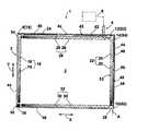
- FIG. 1is a front view of a touch panel 3 , to be utilized in an apparatus 1 .
- the touch panel 3comprises: a substrate 2 formed by a rectangular glass plate; a Flexible Printed Circuit 4 (FPC) mounted on the substrate 2 ; and a controller 6 , which is electrically linked to the FPC 4 .
- FPCFlexible Printed Circuit
- the FPC 4is branched into an FPC branch 4 a and an FPC branch 4 b .
- the FPC branch 4 aextends along the horizontal direction of the substrate 2 , that is, the X axis direction indicated by the arrow X.
- the FPC branch 4 bextends along the vertical direction of the substrate perpendicular to the X axis, that is, the Y axis direction indicated by the arrow Y.
- Converters (bulk wave generating means) 8 and 10 for generating ultrasonic wavesare mounted on the FPC 4 .
- converters (detectors) 12 and 14which function as sensors, are mounted on the FPC 4 .
- a reflection array 18comprising a great number of inclined lines 16 , is formed along the Y axis on the front surface of the substrate 2 , in the vicinity of one lateral edge 44 thereof.
- a reflection array 22comprising a great number of inclined lines 20 , is formed to face the reflection array 18 , at the other lateral edge 44 of the substrate.
- a reflection array 28comprising a great number of inclined lines 26 , is formed along the X axis in the vicinity of the upper edge 24 of the substrate 2 .
- a reflection array 32comprising a great number of inclined lines 30 , is formed to face the reflection array 28 , in the vicinity of the lower edge 45 of the substrate.
- the patterns of these reflection arrays 18 , 22 , 28 , and 32are those disclosed in Japanese Unexamined Patent Publication Nos. 61 (1986)-239322 and 2001-14094. Note that the reflection arrays 18 , 22 , 28 , and 32 are collectively referred to as a reflection array 33 .
- the reflection array 33reflects acoustic waves, and causes them to propagate along the front surface of the substrate 2 .
- the converters 8 , 10 , 12 , and 14are adhesively attached to the rear surface of the substrate 2 .
- Mode converting elements 78 , 80 , 82 , and 84are formed on the front surface of the substrate 2 , at positions corresponding to the converters 8 , 10 , 12 , and 14 , respectively.
- FIG. 11is a schematic partially magnified view of the substrate 2 , viewed from the direction of arrow A.
- the mode converting element 80 of FIG. 11is formed by sintering glass paste on the substrate 2 , and comprises a plurality of parallel ridges 80 a .
- the ridges 80 a shown in FIG. 11extend in the direction perpendicular to the surface of the drawing sheet.
- the widths of the ridges 80 aare set to be 400 ⁇ m, and the heights are set to be 35 ⁇ m or greater.
- the direction in which the bulk waves are reflectedis changed by varying the intervals among the ridges 80 a .
- the ridges 80 aare formed with intervals that cause surface acoustic waves to be generated directly beside the ridges 80 a .
- the converter 10is adhesively attached on the side of the substrate opposite the mode converting element 80 , and is electrically connected to the FPC branch 4 b with solder.
- the other mode converting elements 78 , 82 , and 84are of the same construction.
- the mode converting elements (acoustic wave generating means) denoted by reference numerals 78 and 80convert bulk waves generated by the transmission side converters 8 and 10 into surface acoustic waves.
- the mode converting elements 82 and 84convert the surface acoustic waves which have propagated along the front surface of the substrate 2 back into bulk waves.
- the converter 10generates ultrasonic vibrations (bulk waves) at a frequency of approximately 5.5 MHz.
- the ultrasonic vibrationstravel through the interior of the substrate 2 from the rear surface thereof, and reach the mode converting element 80 .
- the mode converting element 80converts the ultrasonic vibrations to surface acoustic waves, which are propagated (reflected) perpendicular to the ridges 80 a , toward the reflection array 32 .
- the surface acoustic wavesare reflected by the inwardly inclined lines 30 of the reflection array 32 and propagate along the front surface of the substrate 2 toward the reflection array 28 until they reach the inwardly inclined lines 26 .
- Bulk waves which are not converted to surface acoustic waves by the mode converting elements 78 and 80are not radiated in a specific direction, but propagate in all directions from the mode converting elements 78 and 80 . If a portion of the unconverted bulk waves are transmitted to the converters 12 and 14 , they become spurious waves that obstruct primary signal detection.
- the mode converting elements 78 and 80are constructed to generate surface acoustic waves in a direction perpendicular to the ridges thereof, it is known that slight surface acoustic waves are generated in unintended directions. These surface acoustic waves may also become spurious waves that obstruct primary signal detection. If these spurious waves reach the converters 12 and 14 , noise signals are generated thereat.
- the surface acoustic waves that reach the reflection array 28are reflected thereby to propagate toward the mode converting element 84 .
- the surface acoustic waves that reach the mode converting element 84are converted to bulk waves thereby.
- the converted bulk wavesare transmitted to the converter 14 on the rear surface of the substrate 2 , which senses and converts the vibrations thereof to electrical signals.
- the ultrasonic vibrations (bulk waves) generated by the converter 8are converted to surface acoustic waves by the mode converting element 78 . Then, the surface acoustic waves reach the mode converting element 82 via the reflection array 18 and the reflection array 22 . The surface acoustic waves are converted to bulk waves by the mode converting element 82 , transmitted to the converter 14 , which senses and converts them to electrical signals.
- the surface acoustic wavesare propagated across the entire region of the front surface of the substrate 2 covered by the reflection arrays 18 , 22 , 28 , and 32 . Therefore, if a finger (object) contacts (touches) the substrate 2 within this region, the surface acoustic waves blocked by the finger disappear or are attenuated.
- the signal change accompanying the change in the surface acoustic wavesis transmitted from the converters 12 and 14 , which function as sensors, to a timing circuit of the controller 6 connected thereto. The controller 6 determines the geometric coordinates of the position touched by the finger.
- the surface acoustic wavesare reflected by each of the inclined lines 16 , 20 , 26 , and 30 of the reflection array 33 . 0.5% to 1% of the surface acoustic waves that reach each of the inclined lines are reflected thereby. The remainder passes through and is transmitted to the adjacent inclined line, so that all of the inclined lines sequentially reflect the surface acoustic waves.
- Spurious wave scattering means for reducing noise by diffusing spurious wavesare formed on the front surface of the substrate 2 of the apparatus 1 .
- the diffusion gratingsinclude the rectangular portions denoted by reference numerals 34 , 36 , and 38 in FIG. 1 , a diffusion grating 43 formed by inclined lines 40 and 42 along the upper edge 24 , and a diffusion grating 49 formed by inclined lines 46 and 48 along the lateral edge 44 .
- the inclined lines 40 , 42 , 46 , and 48construct a second reflection array, having a function different from that of the reflection arrays 18 , 22 , 28 , and 32 .
- the second reflection arrayis also provided within the diffusion gratings 34 , 36 , and 3 B (refer to FIG. 7 ). Details of the diffusion gratings 34 , 36 , 38 , 43 , and 49 will be described later. Note that the diffusion gratings will collectively be referred to as a diffusion grating 50 .
- FIG. 2is a front view illustrating the FPC 4 , which is attached to the substrate 2 .
- the FPC 4is adhesively attached to the rear surface of the substrate 2 , it is drawn in solid lines for the sake of convenience. Note that the reflection array 33 and the diffusion grating 50 are omitted from FIG. 2 .
- FIG. 3is a schematic plan view showing the entirety of the FPC 4 .
- FIG. 4is a magnified view of the portion of the FPC 4 indicated by B in FIG. 3 .
- the FPC 4 as shown in FIG. 3 and FIG. 4correspond to a state in which it is viewed from the rear surface of the substrate 2 of FIG. 2 .
- Electrodes 52 and 54corresponding respectively to the converters (sensors) 12 and 14 , are provided at one end of the FPC 4 , as shown in FIG. 3 and FIG. 4 .
- the electrodes 52 and 54are connected to the converters 12 and 14 from above by soldering, a conductive adhesive such as silver paste, or an anisotropic conductive adhesive. That is, the converters 12 and 14 are positioned between the FPC 4 and the rear surface of the substrate 2 .
- the FPC 4is constructed by the aforementioned FPC branches 4 a and 4 b , and a connection line 4 c for connecting with the controller 6 .
- connection line 4 c and the FPC branch 4 aare of the same length, and are formed integrally as a band (refer to FIG. 3 ). Perforations 56 are formed between the connection line 4 c and the FPC branch 4 a , to enable separation of the two.
- An electrode 58for connecting with the converter 8 , is formed at the end of the FPC branch 4 a opposite that at which the electrode 52 is provided.
- An electrode 60for connecting with the controller 6 , is formed at the end of the connection line 4 c near the electrode 58 .
- An electrode 62for connecting with the converter 10 , is formed at the end of the FPC branch 4 b opposite that at which the electrode 54 is provided (refer to FIG. 3 ).
- a printed wiring 64 of the connection line 4 ccomprises ten printed wires 64 a , 64 b , 64 c , 64 d , 64 e , 64 f , 64 g , 64 h , 64 i , and 64 j .
- a signal wire groupis constructed by four printed wires (signal reception wires) 64 d , 64 e , 64 f , and 64 g , which are connected to the converters (sensors). 12 and 14 . What is important here is that grounding wires 64 c and 64 h are provided at either side of the signal wire group.
- Signal wires 64 b and 64 iwhich are connected to the transmission converters 8 and 10 , are provided adjacent to the grounding wires 64 c and 64 h , respectively. Further, grounding wires 64 a and 64 j are provided adjacent to the signal wires 64 b and 64 i , respectively on the outsides thereof. This construction results in shielding of all of the signal wires, by the signal reception wires 64 d , 64 e , 64 f , and 64 g being surrounded by the grounding wires 64 c and 64 h , and the signal transmission wires 64 b and 64 i being surrounded by the grounding wires 64 c and 64 a , and the grounding wires 64 h and 64 j , respectively.
- the signal wire group consisting of the printed wires 64 b , 64 d , 64 e , 64 f , 64 g , and 64 iare less likely to be influenced by external electromagnetic waves. At the same time, an effect that electromagnetic waves are less likely to be radiated toward the exterior is also obtained.
- the above constructionis particularly effective in improving anti-EMI properties in the case that the FPC 4 is extended over a long distance along the substrate 2 .
- bending lines of the FPC branch 4 bare denoted by reference numerals 66 and 68 in FIG. 4 .
- the FPC branch 4 bis bent along the bending line 66 in the direction toward the surface of the drawing sheet of FIG. 4 .
- the FPC branch 4 bis bent again along the bending line 68 in the direction away from the surface of the drawing sheet of FIG. 4 , so that the electrode 62 (refer to FIG. 3 ) faces the converter 10 .
- the bending portionis denoted by reference numeral 69 in FIG. 2 .
- the FPC branch 4 bis arranged along the lateral edge 44 of the substrate 2 .
- the FPC 4is fixed to the substrate 2 by an adhesive (not shown) or the like.
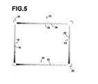
- FIG. 5is a front view of the reflection array 33 , corresponding to that shown in FIG. 1 .
- the diffusion gratings 34 , 36 , 38 , and the like for scattering spurious wavesare omitted from FIG. 5 .
- Each of the inclined lines 16 , 20 , 26 , and 30 of the reflection arrays 18 , 22 , 28 , and 32is inclined at an angle of 45°.
- the inclined lines 16 , 20 , 26 , and 30are configured to reflect surface acoustic waves toward the reflection array that faces them across the substrate 2 .
- the reflection array 33is formed by printing fine particles of lead glass formed into a paste on the front surface of the substrate 2 by screen printing or the like, then sintering at approximately 500° C. Note that the corners of the substrate 2 are partially illustrated in FIG. 5 , denoted by reference numeral 25 .
- a UV curable organic ink, or an organic ink having metal particles added as filler therein to improve the reflective properties thereof,may be utilized as the material of the reflection array.
- the intervals among the inclined lines 16 , 20 , 26 , and 30decrease, that is, the incline lines are arranged at higher densities, the further they are from the transmission side converters 8 and 10 .
- the reflection arrays 22 and 28are provided slightly inward from the upper edge 24 and the lateral edge 44 (refer to FIG. 1 ) of the substrate, respectively. This is so that the inclined lines 40 , 42 , 46 , and 48 of the diffusion grating 50 , to be described later, may be provided at the outsides of the reflection arrays 22 and 28 .
- FIG. 6is a front view, corresponding to FIG. 1 , that shows the diffusion grating 50 along with the mode converting elements 78 , 80 , 82 , and 84 .
- the inclined lines 40 and 42which constitute the second reflection array, are formed at opposite angles with respect to each other in the vicinity of the upper edge 24 of the substrate 2 .
- the angles of the inclined linesare such that they are close to perpendicular toward the central portion of the substrate 2 , and gradually decrease toward the edges thereof.
- the other inclined lines 46 and 48which constitute the second reflection array, are formed at opposite angles with respect to each other, with gradually changing angles. This is so that spurious waves are not reflected in the same direction, but rather are diffused.
- the inclined lines 40 , 42 , 46 , and 48are positioned at regions where tape and the like are adhered to in conventional touch panels. That is, the inclined lines 40 , 42 , 46 , and 48 are formed to replace the tape of conventional touch panels.
- the spurious waves that reach these regionsare diffusively reflected by the inclined lines 40 , 42 , 46 , and 48 , so that they are not propagated to the converters (sensors) 12 and 14 .
- the attenuation rate of ultrasonic vibration energydiffers according to the frequency of the ultrasonic waves, the vibration mode, and the type of glass.
- the intensity of surface acoustic waves at a frequency of 5.5 MHzattenuates to 1/10 its original intensity after propagating 40 cm along a typical substrate 2 formed of soda lime glass. Accordingly, the diffusively reflected spurious waves attenuate rapidly and disappear as they are reflected across the substrate 2 .
- FIG. 7is a partial magnified view of the diffusion grating 36 and the reflection array 33 .
- FIG. 8is a partial magnified view of the diffusion grating 38 and the reflection array 33 . It is clearly shown in FIG. 7 that inclined lines 36 a of the diffusion grating 36 are oriented at angles different from those of the reflection arrays 18 and 32 .
- FIG. 8clearly shows the diffusion grating 38 , which is constituted by steeply inclined lines 38 a.
- diffusion gratings 36 and 38also function to diffusively reflect spurious waves that propagate along the front surface of the substrate 2 toward the exterior, at angles other than 45° or ⁇ 45°.
- the diffusion grating 34although not illustrated in detail, possesses a similar structure and function.
- the inclined lines 36 a and 38 amay be parallel or have gradually changing angles within the respective diffusion gratings 36 and 38 .
- the diffusion gratings 34 and 38also function to block the paths of surface acoustic waves that propagate in directions other than a predetermined direction, so that they do not reach the converters (sensors) 12 and 14 .
- the diffusion grating 50is printed on the substrate 2 by lead glass particles formed into a paste, in the same manner as the reflection array 33 . Accordingly, the diffusion grating 50 may be printed at the same time that the reflection array 33 is formed. This improves productivity and reduces manufacturing costs.
- the inclined lines 36 a and 38 a of the diffusion gratings 36 and 38are formed as a plurality of ridges.
- the diffusion gratingsare not limited to being formed by ridges, and various modifications are possible.
- An alternate construction of the diffusion gratingis shown in FIG. 9 .
- FIG. 9is a magnified view of an alternate form of the diffusion grating.
- This diffusion grating 51is constructed by a great number of protrusions 51 a , which are diamond shaped in plan view. Spurious waves that reach the diffusion grating 51 are attenuated while being repetitively reflected by the protrusions 51 a within the region formed thereby.
- the shape of the protrusionsis not limited to a diamond shape, and may be any desired shape, such as rectangles, triangles, other polygonal shapes, or ovals.
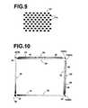
- FIG. 10is a front view illustrating the relative positions of the diffusion grating 50 and the reflection array 33 , formed on the front surface of the substrate 2 .
- FIG. 10clearly illustrates that the inclined lines 40 and 42 are positioned outside the reflection array 28 , and that the inclined lines 46 and 48 are positioned outside the reflection array 22 .
- the diffusion gratings 34 , 36 , and 38are positioned so that surface acoustic waves, which pass through the reflection array 33 without being reflected, are reflected in directions different from those in which the reflection array 33 reflects them.
- the diffusion grating 36functions to reflect surface acoustic waves toward the outside of the substrate 2 . That is, the diffusion grating 36 reflects the surface acoustic waves in the opposite direction from the primary direction, so that ultrasonic vibrations that would cause noise do not reach the converter (sensor) 12 .
- the inclined lines 40 , 42 , 46 , and 48 formed along the edges of the substrate 2are structured to diffusively reflect and attenuate bulk waves that propagate along the front surface of the substrate 2 .
- bulk wavesare converted to surface acoustic waves by the mode converting elements 78 and 80 .
- the inclined lines 40 , 42 , 46 , and 48are utilized to attenuate these spurious bulk waves.
- surface acoustic wavespropagate in directions other than the predetermined directions therefor after being converted by the mode converting elements 78 and 80 .
- the inclined lines 40 , 42 , 46 , and 48also diffusively reflect these stray surface acoustic waves so that they are scattered in various directions. The risk that spurious ultrasonic vibrations reach the converters (sensors) 12 and 14 to cause noise is reduced by this diffusive reflection.
- Pictures 82 of dolphinsare printed between the inclined lines 40 and 42 , and also between the inclined lines 46 and 48 in FIG. 10 .
- the pictures 82are also effective in reducing noise.
- the pictures 82have curved outlines. Bulk waves or stray surface acoustic waves that reach the outlines of the pictures 82 are reflected in various directions and attenuated. Any picture may be employed as long as the outline thereof is formed of curved lines, or are of angles that cause spurious waves to be diffusively reflected in various directions. Alternatively, patterns may be printed on the substrate 2 at these portions.
- FIG. 12is a partial magnified view of a touch panel in which an inclined surface is formed at the edge of a glass substrate, and a converter is mounted on the inclined surface.
- An upwardly facing inclined surface 94is formed along the entire lengths of the edges of a substrate 90 of a touch panel 92 of this second embodiment, corresponding to the upper edge 24 and the lateral edge 44 of the previous embodiment.
- a converter 98which is triangular in cross section (wedge type converter) is adhesively attached to the inclined surface 94 .
- An FPC 96is adhesively attached to the rear surface 90 a of the substrate 90 .
- a portion 96 a of the FPC 96extends outward and is connected to the converter 98 via an electrode 99 .
- reference numeral 97denotes a piezoelectric element which is a part of the converter 98 .
- the converter 98may be a transmission converter or a reception converter.
- the FPC 96may alternatively be provided on the inclined surface 94 .
- the converter 98is a transmission converter
- ultrasonic vibrations generated therebyare propagated upward along the inclined surface 94 , then along the front surface 90 b of the substrate 90 , as indicated by arrow 95 .
- Acoustic waves that propagate along the front surface 90 bare changed by contact with a finger or a like. The change is detected and the touched position is determined in the same manner as in the previous embodiment.
- the converter 98is provided on the inclined surface 94 of the substrate 90 . Therefore, the converter 98 does not protrude from the substrate 90 , and is easily accommodated within bezels, even if the periphery of the substrate 90 is covered with bezels or the like.
- FIG. 13is a front view of an FFC 100 which is attached to the substrate 2 .
- FIG. 14is a partial magnified view of the FFC 100 of FIG. 13 .
- FIG. 15is a schematic magnified sectional view of the FFC 100 . As shown in FIG. 15 , the FFC 100 comprises three flat linear conductors.
- the three flat linear conductorsare two substantially parallel signal wires 104 and 104 , and a grounding wire 102 provided between the two signal wires 104 , substantially parallel thereto.
- the signal wires 104 and the grounding wire 102are covered by a flat insulator 106 , thereby insulated from each other. By this construction, the signal wires 104 are shielded by the grounding wire 102 .
- the outer periphery of the insulator 106is covered by a conductive film 108 such as copper plating, which is electrically connected to the grounding wire 102 via a connection portion 108 a .
- a conductive film 108such as copper plating
- the two signal wires 104are shielded by the film 108 in addition to the grounding wire 102 , further improving the anti-EMI properties.
- the film 108is covered and protected by an insulative outer covering 110 .
- Two FFC's 100 constructed in this mannerare utilized on the substrate 2 , as shown in FIG. 13 and FIG. 14 . That is, an FFC 100 a is provided at the upper edge 24 of the substrate 2 , and an FFC 100 b is provided at the lateral edge 44 .
- the FFC 100 a and the FFC 100 bare connected via a rigid circuit board 112 .
- An electrical connector 114is mounted on the rigid circuit board 112 .
- the electrical connector 114functions to establish an electrical connection with the controller 6 , via an FFC 100 partially shown by broken lines.
- the direction of the FFC 100 bis changed by being folded from the lateral edge 44 toward the upper edge 24 .
- the converters 12 and 14are connected to the rigid circuit board 112 via conductors 116 and 116 .
- the converters 8 and 10are electrically connected to the distal ends of the FFC's 100 a and 10 b , respectively, by soldering.
- the FFC 100 , the converters 8 , 10 , 12 , and 14 , as well as the rigid circuit board 112are adhesively attached to the substrate 2 .
- the rigid circuit board 112may be replaced by an FPC.
- the wiring for connecting the electrical connector 114 and the connector 6is not limited to the FFC 100 .
- An FPC, a bifilar wire (to be described later), or an FFC, from which the conductive film 108 and the insulative outer covering 110 shown in FIG. 15 are removed, that is, an FFC comprising the grounding wire 102 , the signal wires 104 , and the insulator 106 ,may alternatively be employed.
- FIG. 16is a front view of an FFC 130 which is attached to the substrate.
- FIG. 17is a partial magnified view of the FFC 130 of FIG. 16 .
- FIG. 18is a schematic magnified sectional view of the FFC 130 of FIG. 16 .
- the FFC 130comprises two flat conductors.
- the two flat conductorsare a signal wire 132 and a grounding wire 134 , arranged parallel to each other.
- the periphery of the signal wire 132 and the grounding wire 134is covered by an insulator 136 .
- the insulator 136is further covered by an outer covering 138 , although this outer covering 138 is not always necessary.
- the film 108 of the previous embodiment illustrated in FIG. 13 through FIG. 15has been omitted.
- the signal wire 132is in a state in which it is shielded by the grounding wire 134 .
- the FFC 130comprises an FFC 130 a , which is adhesively attached at the upper edge 24 of the substrate 2 , and an FFC 130 b , which is adhesively attached at the lateral edge 44 .
- the FFC 130 a and the FFC 130 bare electrically connected via a rigid circuit board 140 .
- the rigid circuit board 140comprises a main body 140 a along the upper edge 24 , and an arm portion 140 b that extends toward the lateral edge 44 .
- the FFC 130 ais connected to the main body 140 a by soldering.
- the FFC 130 bis connected to the arm portion 140 b .
- the converters 12 and 14are electrically connected to the rigid circuit board 140 via an FFC 130 c and an FFC 130 d , respectively.
- a connector 142for connecting the rigid circuit board 140 with the controller 6 via an FFC 130 , is mounted on the rigid circuit board 140 .
- the FFC 130is only partly shown by broken lines in FIG. 17 , and the controller 6 is omitted.
- the rigid circuit board 140may be replaced by an FPC.
- the wiring for connecting the electrical connector 142 to the controller 6may be an FPC or a bifilar wire, as alternatives to the FFC 130 .
- the cost of the apparatuses according to the third and fourth embodimentscan be reduced as a whole.
- the rigid circuit boards 112 and 140are employed, separate conductors such as the FFC 130 are required to connect the converters 8 , 10 , 12 , and 14 thereto.
- the converters 8 , 10 , 12 , and 14may be directly soldered thereon.
- Wires having extremely small cross sectional areassuch as that of AWG 40 (diameter of about 0.5 mm), that is, bifilar wires, may be utilized in place of the FFC's 100 and 130 .
- the bifilar wiresare single wires that comprise a pair of twisted or parallel conductors, insulated from each other. As the diameters thereof are extremely small, the bifilar wires do not protrude significantly even if they are provided on the surface of the substrate 2 .
- the pair of conductors of the bifilar wirescomprises a signal wire and a grounding wire adjacent to each other. Thereby, a shielding effect is obtained by this structure.
- the diffusion grating 50may be formed by etching with hydrofluoric acid.
- the diffusion grating 50may also be formed by a chemical or physical removal process employing lasers, sandblasting, or cutting.
- the diffusion grating 50may be formed by grooves instead of protrusions.
- the present inventionis not limited to apparatuses that employ this type of surface acoustic wave generating means.
- the present inventionmay be applied to an acoustic wave contact detecting apparatus that generates surface acoustic waves by means of a wedge type converter as shown in FIG. 12 that utilizes an acrylic prism.
- the present inventionmay also be applied to an acoustic wave contact detecting apparatus that employs a pair of comb electrodes formed on an ultrasonic vibrator, without a grating nor a wedge.
- ultrasonic vibrationsare transmitted in the edge direction of the ultrasonic vibrator and not in the thickness direction thereof. Therefore, the ultrasonic vibrator can be provided on the same surface as the mode converting elements 78 , 80 , 82 , and 84 .
- the FPC 4 which is utilized in the present inventionmay be adhesively attached to the substrate 2 with any desired adhesive.
- piezoelectric vibratorsbe adhesively attached using ultraviolet cured adhesive. This is to enable adjustment of the positions of the converters 8 , 10 , 12 , and 14 with respect to the mode converting elements 78 , 80 , 82 and 84 to confirm optimal generation of surface acoustic waves prior to irradiation of ultraviolet rays, which causes adhesion.
- the spurious wave scattering meansmay be of the type that causes diffusive reflection and attenuation, as described above.
- the two converters (sensors) 12 and 14are provided in close proximity to each other in the embodiments described above.
- the converters (sensors) 12 and 14may switch places with the transmission converters 8 and 10 , so that they are positioned apart from each other. In this case, when surface acoustic waves leak from either the converter 12 or 14 , as the other converter 14 or 12 is not in close proximity therewith, the noise picked up by the other converter is suppressed.
- the electrical path from the controller 6 to the transmission converters 8 and 10can be reduced. Therefore, spurious radiation, that is, emission of electromagnetic waves, from the electrical path, can be suppressed.
Landscapes
- Engineering & Computer Science (AREA)
- Physics & Mathematics (AREA)
- General Engineering & Computer Science (AREA)
- Theoretical Computer Science (AREA)
- General Physics & Mathematics (AREA)
- Human Computer Interaction (AREA)
- Electromagnetism (AREA)
- Microelectronics & Electronic Packaging (AREA)
- Acoustics & Sound (AREA)
- Position Input By Displaying (AREA)
- Transducers For Ultrasonic Waves (AREA)
- Length Measuring Devices Characterised By Use Of Acoustic Means (AREA)
- Measurement Of Velocity Or Position Using Acoustic Or Ultrasonic Waves (AREA)
Abstract
Description
- a substrate having a surface along which acoustic waves propagate;
- an acoustic wave generating means;
- a reflection array for causing the generated acoustic waves to propagate along the surface of the substrate;
- a detector for detecting changes in the acoustic wave caused by an object contacting the surface of the substrate; and
- a controller for determining the geometric coordinates of the object; wherein:
- at least one of the acoustic wave generating means and the detector are connected the controller by flexible planar wiring; and
- the flexible planar wiring is of a wiring pattern in which a grounding wire is provided on at least one side of a signal wire.
- a signal wire group in which a plurality of the signal wires are arranged; and
- grounding wires at both sides of the signal wire group.
Claims (10)
Priority Applications (6)
| Application Number | Priority Date | Filing Date | Title |
|---|---|---|---|
| TW093134182ATW200532171A (en) | 2003-11-12 | 2004-11-09 | Acoustic wave contact detecting apparatus |
| KR1020067011500AKR20070011248A (en) | 2003-11-12 | 2004-11-10 | Acoustic Wave Contact Detection Device |
| PCT/US2004/037563WO2005050546A2 (en) | 2003-11-12 | 2004-11-10 | Acoustic wave touch detecting apparatus |
| EP04810706AEP1690178A2 (en) | 2003-11-12 | 2004-11-10 | Acoustic wave touch detecting apparatus |
| CNA2004800398155ACN1906566A (en) | 2003-11-12 | 2004-11-10 | Acoustic wave type touch detection device |
| JP2006539826AJP2007512594A (en) | 2003-11-12 | 2004-11-10 | Sonic touch detector |
Applications Claiming Priority (2)
| Application Number | Priority Date | Filing Date | Title |
|---|---|---|---|
| JP2002329478AJP2004163262A (en) | 2002-11-13 | 2002-11-13 | Acoustic wave contact detector |
| JP2002-329478 | 2002-11-13 |
Publications (2)
| Publication Number | Publication Date |
|---|---|
| US20050035685A1 US20050035685A1 (en) | 2005-02-17 |
| US6948371B2true US6948371B2 (en) | 2005-09-27 |
Family
ID=32310570
Family Applications (1)
| Application Number | Title | Priority Date | Filing Date |
|---|---|---|---|
| US10/712,753Expired - LifetimeUS6948371B2 (en) | 2002-11-13 | 2003-11-12 | Acoustic wave touch detecting apparatus |
Country Status (8)
| Country | Link |
|---|---|
| US (1) | US6948371B2 (en) |
| EP (1) | EP1562104A4 (en) |
| JP (1) | JP2004163262A (en) |
| KR (1) | KR20050086550A (en) |
| CN (1) | CN1327320C (en) |
| AU (1) | AU2003301927A1 (en) |
| TW (1) | TWI291014B (en) |
| WO (1) | WO2004044726A1 (en) |
Cited By (149)
| Publication number | Priority date | Publication date | Assignee | Title |
|---|---|---|---|---|
| US20070240913A1 (en)* | 2006-04-18 | 2007-10-18 | Schermerhorn Jerry D | Touch control system and apparatus with multiple acoustic coupled substrates |
| US20080030483A1 (en)* | 2006-08-03 | 2008-02-07 | Samsung Electronics Co., Ltd. | Touch screen panel, method of manufacturing the same, and display having the same |
| US20100064586A1 (en)* | 2007-02-05 | 2010-03-18 | Nice Spa | Motor unit for a gate actuating system |
| US20100194711A1 (en)* | 2009-02-05 | 2010-08-05 | Quanta Computer, Inc. | Optical Touch Sensing Apparatus |
| WO2013044253A1 (en)* | 2011-08-19 | 2013-03-28 | Butler David J | Safety system for machine tools |
| US9189109B2 (en) | 2012-07-18 | 2015-11-17 | Sentons Inc. | Detection of type of object used to provide a touch contact input |
| US9348468B2 (en) | 2013-06-07 | 2016-05-24 | Sentons Inc. | Detecting multi-touch inputs |
| US9449476B2 (en) | 2011-11-18 | 2016-09-20 | Sentons Inc. | Localized haptic feedback |
| US9459715B1 (en) | 2013-09-20 | 2016-10-04 | Sentons Inc. | Using spectral control in detecting touch input |
| US9477350B2 (en) | 2011-04-26 | 2016-10-25 | Sentons Inc. | Method and apparatus for active ultrasonic touch devices |
| US9513727B2 (en) | 2012-07-18 | 2016-12-06 | Sentons Inc. | Touch input surface microphone |
| US9524063B2 (en) | 2012-07-18 | 2016-12-20 | Sentons Inc. | Detection of a number of touch contacts of a multi-touch input |
| US9588552B2 (en) | 2013-09-11 | 2017-03-07 | Sentons Inc. | Attaching electrical components using non-conductive adhesive |
| US9594450B2 (en) | 2011-11-18 | 2017-03-14 | Sentons Inc. | Controlling audio volume using touch input force |
| US9639213B2 (en) | 2011-04-26 | 2017-05-02 | Sentons Inc. | Using multiple signals to detect touch input |
| US9667317B2 (en) | 2015-06-15 | 2017-05-30 | At&T Intellectual Property I, L.P. | Method and apparatus for providing security using network traffic adjustments |
| US9674711B2 (en) | 2013-11-06 | 2017-06-06 | At&T Intellectual Property I, L.P. | Surface-wave communications and methods thereof |
| US9685992B2 (en) | 2014-10-03 | 2017-06-20 | At&T Intellectual Property I, L.P. | Circuit panel network and methods thereof |
| US9705561B2 (en) | 2015-04-24 | 2017-07-11 | At&T Intellectual Property I, L.P. | Directional coupling device and methods for use therewith |
| US9705610B2 (en) | 2014-10-21 | 2017-07-11 | At&T Intellectual Property I, L.P. | Transmission device with impairment compensation and methods for use therewith |
| US9722318B2 (en) | 2015-07-14 | 2017-08-01 | At&T Intellectual Property I, L.P. | Method and apparatus for coupling an antenna to a device |
| US9729197B2 (en) | 2015-10-01 | 2017-08-08 | At&T Intellectual Property I, L.P. | Method and apparatus for communicating network management traffic over a network |
| US9735833B2 (en) | 2015-07-31 | 2017-08-15 | At&T Intellectual Property I, L.P. | Method and apparatus for communications management in a neighborhood network |
| US9742521B2 (en) | 2014-11-20 | 2017-08-22 | At&T Intellectual Property I, L.P. | Transmission device with mode division multiplexing and methods for use therewith |
| US9742462B2 (en) | 2014-12-04 | 2017-08-22 | At&T Intellectual Property I, L.P. | Transmission medium and communication interfaces and methods for use therewith |
| US9749013B2 (en) | 2015-03-17 | 2017-08-29 | At&T Intellectual Property I, L.P. | Method and apparatus for reducing attenuation of electromagnetic waves guided by a transmission medium |
| US9749053B2 (en) | 2015-07-23 | 2017-08-29 | At&T Intellectual Property I, L.P. | Node device, repeater and methods for use therewith |
| US9748626B2 (en) | 2015-05-14 | 2017-08-29 | At&T Intellectual Property I, L.P. | Plurality of cables having different cross-sectional shapes which are bundled together to form a transmission medium |
| US9769020B2 (en) | 2014-10-21 | 2017-09-19 | At&T Intellectual Property I, L.P. | Method and apparatus for responding to events affecting communications in a communication network |
| US9768833B2 (en) | 2014-09-15 | 2017-09-19 | At&T Intellectual Property I, L.P. | Method and apparatus for sensing a condition in a transmission medium of electromagnetic waves |
| US9769128B2 (en) | 2015-09-28 | 2017-09-19 | At&T Intellectual Property I, L.P. | Method and apparatus for encryption of communications over a network |
| US9780834B2 (en) | 2014-10-21 | 2017-10-03 | At&T Intellectual Property I, L.P. | Method and apparatus for transmitting electromagnetic waves |
| US9787412B2 (en) | 2015-06-25 | 2017-10-10 | At&T Intellectual Property I, L.P. | Methods and apparatus for inducing a fundamental wave mode on a transmission medium |
| US9793951B2 (en) | 2015-07-15 | 2017-10-17 | At&T Intellectual Property I, L.P. | Method and apparatus for launching a wave mode that mitigates interference |
| US9793955B2 (en) | 2015-04-24 | 2017-10-17 | At&T Intellectual Property I, Lp | Passive electrical coupling device and methods for use therewith |
| US9793954B2 (en) | 2015-04-28 | 2017-10-17 | At&T Intellectual Property I, L.P. | Magnetic coupling device and methods for use therewith |
| US9800327B2 (en) | 2014-11-20 | 2017-10-24 | At&T Intellectual Property I, L.P. | Apparatus for controlling operations of a communication device and methods thereof |
| US9820146B2 (en) | 2015-06-12 | 2017-11-14 | At&T Intellectual Property I, L.P. | Method and apparatus for authentication and identity management of communicating devices |
| US9838078B2 (en) | 2015-07-31 | 2017-12-05 | At&T Intellectual Property I, L.P. | Method and apparatus for exchanging communication signals |
| US9838896B1 (en) | 2016-12-09 | 2017-12-05 | At&T Intellectual Property I, L.P. | Method and apparatus for assessing network coverage |
| US9847566B2 (en) | 2015-07-14 | 2017-12-19 | At&T Intellectual Property I, L.P. | Method and apparatus for adjusting a field of a signal to mitigate interference |
| US9847850B2 (en) | 2014-10-14 | 2017-12-19 | At&T Intellectual Property I, L.P. | Method and apparatus for adjusting a mode of communication in a communication network |
| US9853342B2 (en) | 2015-07-14 | 2017-12-26 | At&T Intellectual Property I, L.P. | Dielectric transmission medium connector and methods for use therewith |
| US9860075B1 (en) | 2016-08-26 | 2018-01-02 | At&T Intellectual Property I, L.P. | Method and communication node for broadband distribution |
| US9865911B2 (en) | 2015-06-25 | 2018-01-09 | At&T Intellectual Property I, L.P. | Waveguide system for slot radiating first electromagnetic waves that are combined into a non-fundamental wave mode second electromagnetic wave on a transmission medium |
| US9866276B2 (en) | 2014-10-10 | 2018-01-09 | At&T Intellectual Property I, L.P. | Method and apparatus for arranging communication sessions in a communication system |
| US9866309B2 (en) | 2015-06-03 | 2018-01-09 | At&T Intellectual Property I, Lp | Host node device and methods for use therewith |
| US9871282B2 (en) | 2015-05-14 | 2018-01-16 | At&T Intellectual Property I, L.P. | At least one transmission medium having a dielectric surface that is covered at least in part by a second dielectric |
| US9871283B2 (en) | 2015-07-23 | 2018-01-16 | At&T Intellectual Property I, Lp | Transmission medium having a dielectric core comprised of plural members connected by a ball and socket configuration |
| US9871558B2 (en) | 2014-10-21 | 2018-01-16 | At&T Intellectual Property I, L.P. | Guided-wave transmission device and methods for use therewith |
| US9876570B2 (en) | 2015-02-20 | 2018-01-23 | At&T Intellectual Property I, Lp | Guided-wave transmission device with non-fundamental mode propagation and methods for use therewith |
| US9876264B2 (en) | 2015-10-02 | 2018-01-23 | At&T Intellectual Property I, Lp | Communication system, guided wave switch and methods for use therewith |
| US9876605B1 (en) | 2016-10-21 | 2018-01-23 | At&T Intellectual Property I, L.P. | Launcher and coupling system to support desired guided wave mode |
| US9880671B2 (en) | 2013-10-08 | 2018-01-30 | Sentons Inc. | Damping vibrational wave reflections |
| US9882257B2 (en) | 2015-07-14 | 2018-01-30 | At&T Intellectual Property I, L.P. | Method and apparatus for launching a wave mode that mitigates interference |
| US9887447B2 (en) | 2015-05-14 | 2018-02-06 | At&T Intellectual Property I, L.P. | Transmission medium having multiple cores and methods for use therewith |
| US9893795B1 (en) | 2016-12-07 | 2018-02-13 | At&T Intellectual Property I, Lp | Method and repeater for broadband distribution |
| US9906269B2 (en) | 2014-09-17 | 2018-02-27 | At&T Intellectual Property I, L.P. | Monitoring and mitigating conditions in a communication network |
| US9904535B2 (en) | 2015-09-14 | 2018-02-27 | At&T Intellectual Property I, L.P. | Method and apparatus for distributing software |
| US9912027B2 (en) | 2015-07-23 | 2018-03-06 | At&T Intellectual Property I, L.P. | Method and apparatus for exchanging communication signals |
| US9912033B2 (en) | 2014-10-21 | 2018-03-06 | At&T Intellectual Property I, Lp | Guided wave coupler, coupling module and methods for use therewith |
| US9911020B1 (en) | 2016-12-08 | 2018-03-06 | At&T Intellectual Property I, L.P. | Method and apparatus for tracking via a radio frequency identification device |
| US9912381B2 (en) | 2015-06-03 | 2018-03-06 | At&T Intellectual Property I, Lp | Network termination and methods for use therewith |
| US9913139B2 (en) | 2015-06-09 | 2018-03-06 | At&T Intellectual Property I, L.P. | Signal fingerprinting for authentication of communicating devices |
| US9917341B2 (en) | 2015-05-27 | 2018-03-13 | At&T Intellectual Property I, L.P. | Apparatus and method for launching electromagnetic waves and for modifying radial dimensions of the propagating electromagnetic waves |
| US9929755B2 (en) | 2015-07-14 | 2018-03-27 | At&T Intellectual Property I, L.P. | Method and apparatus for coupling an antenna to a device |
| US9927517B1 (en) | 2016-12-06 | 2018-03-27 | At&T Intellectual Property I, L.P. | Apparatus and methods for sensing rainfall |
| US9948333B2 (en) | 2015-07-23 | 2018-04-17 | At&T Intellectual Property I, L.P. | Method and apparatus for wireless communications to mitigate interference |
| US9954287B2 (en) | 2014-11-20 | 2018-04-24 | At&T Intellectual Property I, L.P. | Apparatus for converting wireless signals and electromagnetic waves and methods thereof |
| US9954286B2 (en) | 2014-10-21 | 2018-04-24 | At&T Intellectual Property I, L.P. | Guided-wave transmission device with non-fundamental mode propagation and methods for use therewith |
| US9967173B2 (en) | 2015-07-31 | 2018-05-08 | At&T Intellectual Property I, L.P. | Method and apparatus for authentication and identity management of communicating devices |
| US9973940B1 (en) | 2017-02-27 | 2018-05-15 | At&T Intellectual Property I, L.P. | Apparatus and methods for dynamic impedance matching of a guided wave launcher |
| US9973416B2 (en) | 2014-10-02 | 2018-05-15 | At&T Intellectual Property I, L.P. | Method and apparatus that provides fault tolerance in a communication network |
| US9991580B2 (en) | 2016-10-21 | 2018-06-05 | At&T Intellectual Property I, L.P. | Launcher and coupling system for guided wave mode cancellation |
| US9998870B1 (en) | 2016-12-08 | 2018-06-12 | At&T Intellectual Property I, L.P. | Method and apparatus for proximity sensing |
| US9999038B2 (en) | 2013-05-31 | 2018-06-12 | At&T Intellectual Property I, L.P. | Remote distributed antenna system |
| US9997819B2 (en) | 2015-06-09 | 2018-06-12 | At&T Intellectual Property I, L.P. | Transmission medium and method for facilitating propagation of electromagnetic waves via a core |
| US10009067B2 (en) | 2014-12-04 | 2018-06-26 | At&T Intellectual Property I, L.P. | Method and apparatus for configuring a communication interface |
| US10020844B2 (en) | 2016-12-06 | 2018-07-10 | T&T Intellectual Property I, L.P. | Method and apparatus for broadcast communication via guided waves |
| US10027397B2 (en) | 2016-12-07 | 2018-07-17 | At&T Intellectual Property I, L.P. | Distributed antenna system and methods for use therewith |
| US10044409B2 (en) | 2015-07-14 | 2018-08-07 | At&T Intellectual Property I, L.P. | Transmission medium and methods for use therewith |
| US10051630B2 (en) | 2013-05-31 | 2018-08-14 | At&T Intellectual Property I, L.P. | Remote distributed antenna system |
| US10048811B2 (en) | 2015-09-18 | 2018-08-14 | Sentons Inc. | Detecting touch input provided by signal transmitting stylus |
| US10069185B2 (en) | 2015-06-25 | 2018-09-04 | At&T Intellectual Property I, L.P. | Methods and apparatus for inducing a non-fundamental wave mode on a transmission medium |
| US10069535B2 (en) | 2016-12-08 | 2018-09-04 | At&T Intellectual Property I, L.P. | Apparatus and methods for launching electromagnetic waves having a certain electric field structure |
| US10090594B2 (en) | 2016-11-23 | 2018-10-02 | At&T Intellectual Property I, L.P. | Antenna system having structural configurations for assembly |
| US10090606B2 (en) | 2015-07-15 | 2018-10-02 | At&T Intellectual Property I, L.P. | Antenna system with dielectric array and methods for use therewith |
| US10103422B2 (en) | 2016-12-08 | 2018-10-16 | At&T Intellectual Property I, L.P. | Method and apparatus for mounting network devices |
| US10126877B1 (en) | 2017-02-01 | 2018-11-13 | Sentons Inc. | Update of reference data for touch input detection |
| US10135146B2 (en) | 2016-10-18 | 2018-11-20 | At&T Intellectual Property I, L.P. | Apparatus and methods for launching guided waves via circuits |
| US10135145B2 (en) | 2016-12-06 | 2018-11-20 | At&T Intellectual Property I, L.P. | Apparatus and methods for generating an electromagnetic wave along a transmission medium |
| US10135147B2 (en) | 2016-10-18 | 2018-11-20 | At&T Intellectual Property I, L.P. | Apparatus and methods for launching guided waves via an antenna |
| US10136255B2 (en) | 2016-12-08 | 2018-11-20 | At&T Intellectual Property I, L.P. | Method and apparatus for proximity sensing on a communication device |
| US10139820B2 (en) | 2016-12-07 | 2018-11-27 | At&T Intellectual Property I, L.P. | Method and apparatus for deploying equipment of a communication system |
| US10148016B2 (en) | 2015-07-14 | 2018-12-04 | At&T Intellectual Property I, L.P. | Apparatus and methods for communicating utilizing an antenna array |
| US10168695B2 (en) | 2016-12-07 | 2019-01-01 | At&T Intellectual Property I, L.P. | Method and apparatus for controlling an unmanned aircraft |
| US10178445B2 (en) | 2016-11-23 | 2019-01-08 | At&T Intellectual Property I, L.P. | Methods, devices, and systems for load balancing between a plurality of waveguides |
| US10198097B2 (en) | 2011-04-26 | 2019-02-05 | Sentons Inc. | Detecting touch input force |
| US10205655B2 (en) | 2015-07-14 | 2019-02-12 | At&T Intellectual Property I, L.P. | Apparatus and methods for communicating utilizing an antenna array and multiple communication paths |
| US10225025B2 (en) | 2016-11-03 | 2019-03-05 | At&T Intellectual Property I, L.P. | Method and apparatus for detecting a fault in a communication system |
| US10224634B2 (en) | 2016-11-03 | 2019-03-05 | At&T Intellectual Property I, L.P. | Methods and apparatus for adjusting an operational characteristic of an antenna |
| US10235004B1 (en) | 2011-11-18 | 2019-03-19 | Sentons Inc. | Touch input detector with an integrated antenna |
| US10243270B2 (en) | 2016-12-07 | 2019-03-26 | At&T Intellectual Property I, L.P. | Beam adaptive multi-feed dielectric antenna system and methods for use therewith |
| US10243784B2 (en) | 2014-11-20 | 2019-03-26 | At&T Intellectual Property I, L.P. | System for generating topology information and methods thereof |
| US10264586B2 (en) | 2016-12-09 | 2019-04-16 | At&T Mobility Ii Llc | Cloud-based packet controller and methods for use therewith |
| US10291334B2 (en) | 2016-11-03 | 2019-05-14 | At&T Intellectual Property I, L.P. | System for detecting a fault in a communication system |
| US10296144B2 (en) | 2016-12-12 | 2019-05-21 | Sentons Inc. | Touch input detection with shared receivers |
| US10298293B2 (en) | 2017-03-13 | 2019-05-21 | At&T Intellectual Property I, L.P. | Apparatus of communication utilizing wireless network devices |
| US10305190B2 (en) | 2016-12-01 | 2019-05-28 | At&T Intellectual Property I, L.P. | Reflecting dielectric antenna system and methods for use therewith |
| US10312567B2 (en) | 2016-10-26 | 2019-06-04 | At&T Intellectual Property I, L.P. | Launcher with planar strip antenna and methods for use therewith |
| US10320586B2 (en) | 2015-07-14 | 2019-06-11 | At&T Intellectual Property I, L.P. | Apparatus and methods for generating non-interfering electromagnetic waves on an insulated transmission medium |
| US10326494B2 (en) | 2016-12-06 | 2019-06-18 | At&T Intellectual Property I, L.P. | Apparatus for measurement de-embedding and methods for use therewith |
| US10326689B2 (en) | 2016-12-08 | 2019-06-18 | At&T Intellectual Property I, L.P. | Method and system for providing alternative communication paths |
| US10340600B2 (en) | 2016-10-18 | 2019-07-02 | At&T Intellectual Property I, L.P. | Apparatus and methods for launching guided waves via plural waveguide systems |
| US10340601B2 (en) | 2016-11-23 | 2019-07-02 | At&T Intellectual Property I, L.P. | Multi-antenna system and methods for use therewith |
| US10340573B2 (en) | 2016-10-26 | 2019-07-02 | At&T Intellectual Property I, L.P. | Launcher with cylindrical coupling device and methods for use therewith |
| US10340603B2 (en) | 2016-11-23 | 2019-07-02 | At&T Intellectual Property I, L.P. | Antenna system having shielded structural configurations for assembly |
| US10340983B2 (en) | 2016-12-09 | 2019-07-02 | At&T Intellectual Property I, L.P. | Method and apparatus for surveying remote sites via guided wave communications |
| US10355367B2 (en) | 2015-10-16 | 2019-07-16 | At&T Intellectual Property I, L.P. | Antenna structure for exchanging wireless signals |
| US10359749B2 (en) | 2016-12-07 | 2019-07-23 | At&T Intellectual Property I, L.P. | Method and apparatus for utilities management via guided wave communication |
| US10361489B2 (en) | 2016-12-01 | 2019-07-23 | At&T Intellectual Property I, L.P. | Dielectric dish antenna system and methods for use therewith |
| US10374316B2 (en) | 2016-10-21 | 2019-08-06 | At&T Intellectual Property I, L.P. | System and dielectric antenna with non-uniform dielectric |
| US10382976B2 (en) | 2016-12-06 | 2019-08-13 | At&T Intellectual Property I, L.P. | Method and apparatus for managing wireless communications based on communication paths and network device positions |
| US10389037B2 (en) | 2016-12-08 | 2019-08-20 | At&T Intellectual Property I, L.P. | Apparatus and methods for selecting sections of an antenna array and use therewith |
| US10389029B2 (en) | 2016-12-07 | 2019-08-20 | At&T Intellectual Property I, L.P. | Multi-feed dielectric antenna system with core selection and methods for use therewith |
| US10411356B2 (en) | 2016-12-08 | 2019-09-10 | At&T Intellectual Property I, L.P. | Apparatus and methods for selectively targeting communication devices with an antenna array |
| US10439675B2 (en) | 2016-12-06 | 2019-10-08 | At&T Intellectual Property I, L.P. | Method and apparatus for repeating guided wave communication signals |
| US10446936B2 (en) | 2016-12-07 | 2019-10-15 | At&T Intellectual Property I, L.P. | Multi-feed dielectric antenna system and methods for use therewith |
| US10498044B2 (en) | 2016-11-03 | 2019-12-03 | At&T Intellectual Property I, L.P. | Apparatus for configuring a surface of an antenna |
| US10530505B2 (en) | 2016-12-08 | 2020-01-07 | At&T Intellectual Property I, L.P. | Apparatus and methods for launching electromagnetic waves along a transmission medium |
| US10535928B2 (en) | 2016-11-23 | 2020-01-14 | At&T Intellectual Property I, L.P. | Antenna system and methods for use therewith |
| US10547348B2 (en) | 2016-12-07 | 2020-01-28 | At&T Intellectual Property I, L.P. | Method and apparatus for switching transmission mediums in a communication system |
| US10585522B2 (en) | 2017-02-27 | 2020-03-10 | Sentons Inc. | Detection of non-touch inputs using a signature |
| US10601494B2 (en) | 2016-12-08 | 2020-03-24 | At&T Intellectual Property I, L.P. | Dual-band communication device and method for use therewith |
| US10637149B2 (en) | 2016-12-06 | 2020-04-28 | At&T Intellectual Property I, L.P. | Injection molded dielectric antenna and methods for use therewith |
| US10650940B2 (en) | 2015-05-15 | 2020-05-12 | At&T Intellectual Property I, L.P. | Transmission medium having a conductive material and methods for use therewith |
| US10694379B2 (en) | 2016-12-06 | 2020-06-23 | At&T Intellectual Property I, L.P. | Waveguide system with device-based authentication and methods for use therewith |
| US10727599B2 (en) | 2016-12-06 | 2020-07-28 | At&T Intellectual Property I, L.P. | Launcher with slot antenna and methods for use therewith |
| US10755542B2 (en) | 2016-12-06 | 2020-08-25 | At&T Intellectual Property I, L.P. | Method and apparatus for surveillance via guided wave communication |
| US10777873B2 (en) | 2016-12-08 | 2020-09-15 | At&T Intellectual Property I, L.P. | Method and apparatus for mounting network devices |
| US10797781B2 (en) | 2015-06-03 | 2020-10-06 | At&T Intellectual Property I, L.P. | Client node device and methods for use therewith |
| US10811767B2 (en) | 2016-10-21 | 2020-10-20 | At&T Intellectual Property I, L.P. | System and dielectric antenna with convex dielectric radome |
| US10819035B2 (en) | 2016-12-06 | 2020-10-27 | At&T Intellectual Property I, L.P. | Launcher with helical antenna and methods for use therewith |
| US10908741B2 (en) | 2016-11-10 | 2021-02-02 | Sentons Inc. | Touch input detection along device sidewall |
| US10916969B2 (en) | 2016-12-08 | 2021-02-09 | At&T Intellectual Property I, L.P. | Method and apparatus for providing power using an inductive coupling |
| US10938108B2 (en) | 2016-12-08 | 2021-03-02 | At&T Intellectual Property I, L.P. | Frequency selective multi-feed dielectric antenna system and methods for use therewith |
| US11009411B2 (en) | 2017-08-14 | 2021-05-18 | Sentons Inc. | Increasing sensitivity of a sensor using an encoded signal |
| US11327599B2 (en) | 2011-04-26 | 2022-05-10 | Sentons Inc. | Identifying a contact type |
| US11580829B2 (en) | 2017-08-14 | 2023-02-14 | Sentons Inc. | Dynamic feedback for haptics |
Families Citing this family (15)
| Publication number | Priority date | Publication date | Assignee | Title |
|---|---|---|---|---|
| JP4090329B2 (en) | 2002-11-13 | 2008-05-28 | タッチパネル・システムズ株式会社 | Acoustic wave contact detector |
| TW591502B (en)* | 2003-03-11 | 2004-06-11 | Onetouch Technologies Co Ltd | Design method of the reflective streaks on ultrasonic touch screen |
| TW200532171A (en)* | 2003-11-12 | 2005-10-01 | Elo Touchsystems Inc | Acoustic wave contact detecting apparatus |
| US8253578B2 (en) | 2006-05-12 | 2012-08-28 | Panasonic Corporation | Smoke sensor of the sound wave type including a smoke density estimation unit |
| JP4809130B2 (en)* | 2006-05-31 | 2011-11-09 | タッチパネル・システムズ株式会社 | Acoustic wave type touch panel |
| JP5178590B2 (en)* | 2009-03-09 | 2013-04-10 | 株式会社ジャパンディスプレイイースト | Touch panel |
| JP5597583B2 (en)* | 2011-03-28 | 2014-10-01 | 太陽誘電株式会社 | Touch panel device and electronic device |
| US9304629B2 (en) | 2011-11-15 | 2016-04-05 | Elo Touch Solutions, Inc. | Radial transducer for acoustic wave touch sensor |
| US9348467B2 (en)* | 2011-11-15 | 2016-05-24 | Elo Touch Solutions, Inc. | Radial layout for acoustic wave touch sensor |
| US9128567B2 (en)* | 2012-11-20 | 2015-09-08 | Elo Touch Solutions, Inc. | Segmented waveguide core touch sensor systems and methods |
| WO2017177408A1 (en)* | 2016-04-14 | 2017-10-19 | Abb Technology Ltd | Gripping head, gripping system and method thereof |
| EP3375408B1 (en)* | 2017-03-14 | 2019-05-15 | 3M Innovative Properties Company | Dental light polymerization device |
| TWI692639B (en)* | 2019-10-03 | 2020-05-01 | 佳世達科技股份有限公司 | Ultrasonic probe |
| TWI733208B (en)* | 2019-10-03 | 2021-07-11 | 佳世達科技股份有限公司 | Ultrasonic probe and manufacturing method thereof |
| WO2024185287A1 (en)* | 2023-03-07 | 2024-09-12 | 株式会社オートネットワーク技術研究所 | Flexible substrate and wiring module |
Citations (6)
| Publication number | Priority date | Publication date | Assignee | Title |
|---|---|---|---|---|
| US5241308A (en)* | 1990-02-22 | 1993-08-31 | Paragon Systems, Inc. | Force sensitive touch panel |
| US6091406A (en)* | 1996-12-25 | 2000-07-18 | Elo Touchsystems, Inc. | Grating transducer for acoustic touchscreens |
| US6406990B1 (en)* | 1999-11-24 | 2002-06-18 | Omron Corporation | Method of mounting a semiconductor chip, circuit board for flip-chip connection and method of manufacturing the same, electromagnetic wave readable data carrier and method of manufacturing the same, and electronic component module for an electromagnetic wave readable data carrier |
| US6567077B2 (en)* | 1998-08-18 | 2003-05-20 | Touch Panel Systems Corporation | Touch panel |
| US6741237B1 (en)* | 2001-08-23 | 2004-05-25 | Rockwell Automation Technologies, Inc. | Touch screen |
| US6765274B2 (en)* | 2002-07-10 | 2004-07-20 | Fujitsu Limited | Semiconductor device having a built-in contact-type sensor and manufacturing method of such a semiconductor device |
Family Cites Families (4)
| Publication number | Priority date | Publication date | Assignee | Title |
|---|---|---|---|---|
| JPH0682301A (en)* | 1992-09-04 | 1994-03-22 | Canon Inc | Vibration detector |
| JPH09152938A (en)* | 1995-11-30 | 1997-06-10 | Sanyo Electric Co Ltd | Coordinate input incorporated display device |
| US5739479A (en)* | 1996-03-04 | 1998-04-14 | Elo Touchsystems, Inc. | Gentle-bevel flat acoustic wave touch sensor |
| JP2000043484A (en)* | 1998-07-30 | 2000-02-15 | Ricoh Co Ltd | Electronic blackboard system |
- 2002
- 2002-11-13JPJP2002329478Apatent/JP2004163262A/enactivePending
- 2003
- 2003-11-11CNCNB2003801029736Apatent/CN1327320C/ennot_activeExpired - Fee Related
- 2003-11-11WOPCT/JP2003/014323patent/WO2004044726A1/enactiveApplication Filing
- 2003-11-11EPEP03811119Apatent/EP1562104A4/ennot_activeCeased
- 2003-11-11AUAU2003301927Apatent/AU2003301927A1/ennot_activeAbandoned
- 2003-11-11KRKR1020057008460Apatent/KR20050086550A/ennot_activeCeased
- 2003-11-12TWTW092131663Apatent/TWI291014B/ennot_activeIP Right Cessation
- 2003-11-12USUS10/712,753patent/US6948371B2/ennot_activeExpired - Lifetime
Patent Citations (6)
| Publication number | Priority date | Publication date | Assignee | Title |
|---|---|---|---|---|
| US5241308A (en)* | 1990-02-22 | 1993-08-31 | Paragon Systems, Inc. | Force sensitive touch panel |
| US6091406A (en)* | 1996-12-25 | 2000-07-18 | Elo Touchsystems, Inc. | Grating transducer for acoustic touchscreens |
| US6567077B2 (en)* | 1998-08-18 | 2003-05-20 | Touch Panel Systems Corporation | Touch panel |
| US6406990B1 (en)* | 1999-11-24 | 2002-06-18 | Omron Corporation | Method of mounting a semiconductor chip, circuit board for flip-chip connection and method of manufacturing the same, electromagnetic wave readable data carrier and method of manufacturing the same, and electronic component module for an electromagnetic wave readable data carrier |
| US6741237B1 (en)* | 2001-08-23 | 2004-05-25 | Rockwell Automation Technologies, Inc. | Touch screen |
| US6765274B2 (en)* | 2002-07-10 | 2004-07-20 | Fujitsu Limited | Semiconductor device having a built-in contact-type sensor and manufacturing method of such a semiconductor device |
Cited By (191)
| Publication number | Priority date | Publication date | Assignee | Title |
|---|---|---|---|---|
| US7764276B2 (en)* | 2006-04-18 | 2010-07-27 | Schermerhorn Jerry D | Touch control system and apparatus with multiple acoustic coupled substrates |
| US20070240913A1 (en)* | 2006-04-18 | 2007-10-18 | Schermerhorn Jerry D | Touch control system and apparatus with multiple acoustic coupled substrates |
| US8451231B2 (en)* | 2006-08-03 | 2013-05-28 | Samsung Display Co., Ltd. | Touch screen panel, method of manufacturing the same, and display having the same |
| US20080030483A1 (en)* | 2006-08-03 | 2008-02-07 | Samsung Electronics Co., Ltd. | Touch screen panel, method of manufacturing the same, and display having the same |
| US20100064586A1 (en)* | 2007-02-05 | 2010-03-18 | Nice Spa | Motor unit for a gate actuating system |
| US20100194711A1 (en)* | 2009-02-05 | 2010-08-05 | Quanta Computer, Inc. | Optical Touch Sensing Apparatus |
| US8294692B2 (en)* | 2009-02-05 | 2012-10-23 | Quanta Computer Inc. | Optical touch sensing apparatus |
| US10877581B2 (en) | 2011-04-26 | 2020-12-29 | Sentons Inc. | Detecting touch input force |
| US9639213B2 (en) | 2011-04-26 | 2017-05-02 | Sentons Inc. | Using multiple signals to detect touch input |
| US11327599B2 (en) | 2011-04-26 | 2022-05-10 | Sentons Inc. | Identifying a contact type |
| US10969908B2 (en) | 2011-04-26 | 2021-04-06 | Sentons Inc. | Using multiple signals to detect touch input |
| US9477350B2 (en) | 2011-04-26 | 2016-10-25 | Sentons Inc. | Method and apparatus for active ultrasonic touch devices |
| US10198097B2 (en) | 2011-04-26 | 2019-02-05 | Sentons Inc. | Detecting touch input force |
| US11907464B2 (en) | 2011-04-26 | 2024-02-20 | Sentons Inc. | Identifying a contact type |
| US12299226B2 (en) | 2011-04-26 | 2025-05-13 | Sentons Inc. | Identifying signal disturbance |
| US10444909B2 (en) | 2011-04-26 | 2019-10-15 | Sentons Inc. | Using multiple signals to detect touch input |
| WO2013044253A1 (en)* | 2011-08-19 | 2013-03-28 | Butler David J | Safety system for machine tools |
| US10235004B1 (en) | 2011-11-18 | 2019-03-19 | Sentons Inc. | Touch input detector with an integrated antenna |
| US10732755B2 (en) | 2011-11-18 | 2020-08-04 | Sentons Inc. | Controlling audio volume using touch input force |
| US9449476B2 (en) | 2011-11-18 | 2016-09-20 | Sentons Inc. | Localized haptic feedback |
| US9594450B2 (en) | 2011-11-18 | 2017-03-14 | Sentons Inc. | Controlling audio volume using touch input force |
| US10162443B2 (en) | 2011-11-18 | 2018-12-25 | Sentons Inc. | Virtual keyboard interaction using touch input force |
| US10248262B2 (en) | 2011-11-18 | 2019-04-02 | Sentons Inc. | User interface interaction using touch input force |
| US11016607B2 (en) | 2011-11-18 | 2021-05-25 | Sentons Inc. | Controlling audio volume using touch input force |
| US10353509B2 (en) | 2011-11-18 | 2019-07-16 | Sentons Inc. | Controlling audio volume using touch input force |
| US11829555B2 (en) | 2011-11-18 | 2023-11-28 | Sentons Inc. | Controlling audio volume using touch input force |
| US11209931B2 (en) | 2011-11-18 | 2021-12-28 | Sentons Inc. | Localized haptic feedback |
| US10055066B2 (en) | 2011-11-18 | 2018-08-21 | Sentons Inc. | Controlling audio volume using touch input force |
| US10698528B2 (en) | 2011-11-18 | 2020-06-30 | Sentons Inc. | Localized haptic feedback |
| US9189109B2 (en) | 2012-07-18 | 2015-11-17 | Sentons Inc. | Detection of type of object used to provide a touch contact input |
| US9823760B2 (en) | 2012-07-18 | 2017-11-21 | Sentons Inc. | Touch input surface speaker |
| US10209825B2 (en) | 2012-07-18 | 2019-02-19 | Sentons Inc. | Detection of type of object used to provide a touch contact input |
| US10466836B2 (en) | 2012-07-18 | 2019-11-05 | Sentons Inc. | Using a type of object to provide a touch contact input |
| US10860132B2 (en) | 2012-07-18 | 2020-12-08 | Sentons Inc. | Identifying a contact type |
| US9524063B2 (en) | 2012-07-18 | 2016-12-20 | Sentons Inc. | Detection of a number of touch contacts of a multi-touch input |
| US9513727B2 (en) | 2012-07-18 | 2016-12-06 | Sentons Inc. | Touch input surface microphone |
| US9999038B2 (en) | 2013-05-31 | 2018-06-12 | At&T Intellectual Property I, L.P. | Remote distributed antenna system |
| US10051630B2 (en) | 2013-05-31 | 2018-08-14 | At&T Intellectual Property I, L.P. | Remote distributed antenna system |
| US9348468B2 (en) | 2013-06-07 | 2016-05-24 | Sentons Inc. | Detecting multi-touch inputs |
| US9588552B2 (en) | 2013-09-11 | 2017-03-07 | Sentons Inc. | Attaching electrical components using non-conductive adhesive |
| US9459715B1 (en) | 2013-09-20 | 2016-10-04 | Sentons Inc. | Using spectral control in detecting touch input |
| US9880671B2 (en) | 2013-10-08 | 2018-01-30 | Sentons Inc. | Damping vibrational wave reflections |
| US9674711B2 (en) | 2013-11-06 | 2017-06-06 | At&T Intellectual Property I, L.P. | Surface-wave communications and methods thereof |
| US9768833B2 (en) | 2014-09-15 | 2017-09-19 | At&T Intellectual Property I, L.P. | Method and apparatus for sensing a condition in a transmission medium of electromagnetic waves |
| US9906269B2 (en) | 2014-09-17 | 2018-02-27 | At&T Intellectual Property I, L.P. | Monitoring and mitigating conditions in a communication network |
| US10063280B2 (en) | 2014-09-17 | 2018-08-28 | At&T Intellectual Property I, L.P. | Monitoring and mitigating conditions in a communication network |
| US9973416B2 (en) | 2014-10-02 | 2018-05-15 | At&T Intellectual Property I, L.P. | Method and apparatus that provides fault tolerance in a communication network |
| US9685992B2 (en) | 2014-10-03 | 2017-06-20 | At&T Intellectual Property I, L.P. | Circuit panel network and methods thereof |
| US9866276B2 (en) | 2014-10-10 | 2018-01-09 | At&T Intellectual Property I, L.P. | Method and apparatus for arranging communication sessions in a communication system |
| US9847850B2 (en) | 2014-10-14 | 2017-12-19 | At&T Intellectual Property I, L.P. | Method and apparatus for adjusting a mode of communication in a communication network |
| US9876587B2 (en) | 2014-10-21 | 2018-01-23 | At&T Intellectual Property I, L.P. | Transmission device with impairment compensation and methods for use therewith |
| US9912033B2 (en) | 2014-10-21 | 2018-03-06 | At&T Intellectual Property I, Lp | Guided wave coupler, coupling module and methods for use therewith |
| US9960808B2 (en) | 2014-10-21 | 2018-05-01 | At&T Intellectual Property I, L.P. | Guided-wave transmission device and methods for use therewith |
| US9780834B2 (en) | 2014-10-21 | 2017-10-03 | At&T Intellectual Property I, L.P. | Method and apparatus for transmitting electromagnetic waves |
| US9954286B2 (en) | 2014-10-21 | 2018-04-24 | At&T Intellectual Property I, L.P. | Guided-wave transmission device with non-fundamental mode propagation and methods for use therewith |
| US9769020B2 (en) | 2014-10-21 | 2017-09-19 | At&T Intellectual Property I, L.P. | Method and apparatus for responding to events affecting communications in a communication network |
| US9871558B2 (en) | 2014-10-21 | 2018-01-16 | At&T Intellectual Property I, L.P. | Guided-wave transmission device and methods for use therewith |
| US9705610B2 (en) | 2014-10-21 | 2017-07-11 | At&T Intellectual Property I, L.P. | Transmission device with impairment compensation and methods for use therewith |
| US9742521B2 (en) | 2014-11-20 | 2017-08-22 | At&T Intellectual Property I, L.P. | Transmission device with mode division multiplexing and methods for use therewith |
| US9749083B2 (en) | 2014-11-20 | 2017-08-29 | At&T Intellectual Property I, L.P. | Transmission device with mode division multiplexing and methods for use therewith |
| US9800327B2 (en) | 2014-11-20 | 2017-10-24 | At&T Intellectual Property I, L.P. | Apparatus for controlling operations of a communication device and methods thereof |
| US9954287B2 (en) | 2014-11-20 | 2018-04-24 | At&T Intellectual Property I, L.P. | Apparatus for converting wireless signals and electromagnetic waves and methods thereof |
| US10243784B2 (en) | 2014-11-20 | 2019-03-26 | At&T Intellectual Property I, L.P. | System for generating topology information and methods thereof |
| US9742462B2 (en) | 2014-12-04 | 2017-08-22 | At&T Intellectual Property I, L.P. | Transmission medium and communication interfaces and methods for use therewith |
| US10009067B2 (en) | 2014-12-04 | 2018-06-26 | At&T Intellectual Property I, L.P. | Method and apparatus for configuring a communication interface |
| US9876571B2 (en) | 2015-02-20 | 2018-01-23 | At&T Intellectual Property I, Lp | Guided-wave transmission device with non-fundamental mode propagation and methods for use therewith |
| US9876570B2 (en) | 2015-02-20 | 2018-01-23 | At&T Intellectual Property I, Lp | Guided-wave transmission device with non-fundamental mode propagation and methods for use therewith |
| US9749013B2 (en) | 2015-03-17 | 2017-08-29 | At&T Intellectual Property I, L.P. | Method and apparatus for reducing attenuation of electromagnetic waves guided by a transmission medium |
| US9831912B2 (en) | 2015-04-24 | 2017-11-28 | At&T Intellectual Property I, Lp | Directional coupling device and methods for use therewith |
| US9705561B2 (en) | 2015-04-24 | 2017-07-11 | At&T Intellectual Property I, L.P. | Directional coupling device and methods for use therewith |
| US9793955B2 (en) | 2015-04-24 | 2017-10-17 | At&T Intellectual Property I, Lp | Passive electrical coupling device and methods for use therewith |
| US10224981B2 (en) | 2015-04-24 | 2019-03-05 | At&T Intellectual Property I, Lp | Passive electrical coupling device and methods for use therewith |
| US9793954B2 (en) | 2015-04-28 | 2017-10-17 | At&T Intellectual Property I, L.P. | Magnetic coupling device and methods for use therewith |
| US9871282B2 (en) | 2015-05-14 | 2018-01-16 | At&T Intellectual Property I, L.P. | At least one transmission medium having a dielectric surface that is covered at least in part by a second dielectric |
| US9748626B2 (en) | 2015-05-14 | 2017-08-29 | At&T Intellectual Property I, L.P. | Plurality of cables having different cross-sectional shapes which are bundled together to form a transmission medium |
| US9887447B2 (en) | 2015-05-14 | 2018-02-06 | At&T Intellectual Property I, L.P. | Transmission medium having multiple cores and methods for use therewith |
| US10650940B2 (en) | 2015-05-15 | 2020-05-12 | At&T Intellectual Property I, L.P. | Transmission medium having a conductive material and methods for use therewith |
| US9917341B2 (en) | 2015-05-27 | 2018-03-13 | At&T Intellectual Property I, L.P. | Apparatus and method for launching electromagnetic waves and for modifying radial dimensions of the propagating electromagnetic waves |
| US9912382B2 (en) | 2015-06-03 | 2018-03-06 | At&T Intellectual Property I, Lp | Network termination and methods for use therewith |
| US10050697B2 (en) | 2015-06-03 | 2018-08-14 | At&T Intellectual Property I, L.P. | Host node device and methods for use therewith |
| US9935703B2 (en) | 2015-06-03 | 2018-04-03 | At&T Intellectual Property I, L.P. | Host node device and methods for use therewith |
| US10797781B2 (en) | 2015-06-03 | 2020-10-06 | At&T Intellectual Property I, L.P. | Client node device and methods for use therewith |
| US9967002B2 (en) | 2015-06-03 | 2018-05-08 | At&T Intellectual I, Lp | Network termination and methods for use therewith |
| US9866309B2 (en) | 2015-06-03 | 2018-01-09 | At&T Intellectual Property I, Lp | Host node device and methods for use therewith |
| US9912381B2 (en) | 2015-06-03 | 2018-03-06 | At&T Intellectual Property I, Lp | Network termination and methods for use therewith |
| US10812174B2 (en) | 2015-06-03 | 2020-10-20 | At&T Intellectual Property I, L.P. | Client node device and methods for use therewith |
| US9913139B2 (en) | 2015-06-09 | 2018-03-06 | At&T Intellectual Property I, L.P. | Signal fingerprinting for authentication of communicating devices |
| US9997819B2 (en) | 2015-06-09 | 2018-06-12 | At&T Intellectual Property I, L.P. | Transmission medium and method for facilitating propagation of electromagnetic waves via a core |
| US9820146B2 (en) | 2015-06-12 | 2017-11-14 | At&T Intellectual Property I, L.P. | Method and apparatus for authentication and identity management of communicating devices |
| US9667317B2 (en) | 2015-06-15 | 2017-05-30 | At&T Intellectual Property I, L.P. | Method and apparatus for providing security using network traffic adjustments |
| US10069185B2 (en) | 2015-06-25 | 2018-09-04 | At&T Intellectual Property I, L.P. | Methods and apparatus for inducing a non-fundamental wave mode on a transmission medium |
| US9787412B2 (en) | 2015-06-25 | 2017-10-10 | At&T Intellectual Property I, L.P. | Methods and apparatus for inducing a fundamental wave mode on a transmission medium |
| US9865911B2 (en) | 2015-06-25 | 2018-01-09 | At&T Intellectual Property I, L.P. | Waveguide system for slot radiating first electromagnetic waves that are combined into a non-fundamental wave mode second electromagnetic wave on a transmission medium |
| US9847566B2 (en) | 2015-07-14 | 2017-12-19 | At&T Intellectual Property I, L.P. | Method and apparatus for adjusting a field of a signal to mitigate interference |
| US9722318B2 (en) | 2015-07-14 | 2017-08-01 | At&T Intellectual Property I, L.P. | Method and apparatus for coupling an antenna to a device |
| US9929755B2 (en) | 2015-07-14 | 2018-03-27 | At&T Intellectual Property I, L.P. | Method and apparatus for coupling an antenna to a device |
| US10205655B2 (en) | 2015-07-14 | 2019-02-12 | At&T Intellectual Property I, L.P. | Apparatus and methods for communicating utilizing an antenna array and multiple communication paths |
| US9853342B2 (en) | 2015-07-14 | 2017-12-26 | At&T Intellectual Property I, L.P. | Dielectric transmission medium connector and methods for use therewith |
| US10148016B2 (en) | 2015-07-14 | 2018-12-04 | At&T Intellectual Property I, L.P. | Apparatus and methods for communicating utilizing an antenna array |
| US9882257B2 (en) | 2015-07-14 | 2018-01-30 | At&T Intellectual Property I, L.P. | Method and apparatus for launching a wave mode that mitigates interference |
| US10044409B2 (en) | 2015-07-14 | 2018-08-07 | At&T Intellectual Property I, L.P. | Transmission medium and methods for use therewith |
| US10320586B2 (en) | 2015-07-14 | 2019-06-11 | At&T Intellectual Property I, L.P. | Apparatus and methods for generating non-interfering electromagnetic waves on an insulated transmission medium |
| US9793951B2 (en) | 2015-07-15 | 2017-10-17 | At&T Intellectual Property I, L.P. | Method and apparatus for launching a wave mode that mitigates interference |
| US10090606B2 (en) | 2015-07-15 | 2018-10-02 | At&T Intellectual Property I, L.P. | Antenna system with dielectric array and methods for use therewith |
| US9806818B2 (en) | 2015-07-23 | 2017-10-31 | At&T Intellectual Property I, Lp | Node device, repeater and methods for use therewith |
| US9912027B2 (en) | 2015-07-23 | 2018-03-06 | At&T Intellectual Property I, L.P. | Method and apparatus for exchanging communication signals |
| US9871283B2 (en) | 2015-07-23 | 2018-01-16 | At&T Intellectual Property I, Lp | Transmission medium having a dielectric core comprised of plural members connected by a ball and socket configuration |
| US9948333B2 (en) | 2015-07-23 | 2018-04-17 | At&T Intellectual Property I, L.P. | Method and apparatus for wireless communications to mitigate interference |
| US9749053B2 (en) | 2015-07-23 | 2017-08-29 | At&T Intellectual Property I, L.P. | Node device, repeater and methods for use therewith |
| US9735833B2 (en) | 2015-07-31 | 2017-08-15 | At&T Intellectual Property I, L.P. | Method and apparatus for communications management in a neighborhood network |
| US9838078B2 (en) | 2015-07-31 | 2017-12-05 | At&T Intellectual Property I, L.P. | Method and apparatus for exchanging communication signals |
| US9967173B2 (en) | 2015-07-31 | 2018-05-08 | At&T Intellectual Property I, L.P. | Method and apparatus for authentication and identity management of communicating devices |
| US9904535B2 (en) | 2015-09-14 | 2018-02-27 | At&T Intellectual Property I, L.P. | Method and apparatus for distributing software |
| US10048811B2 (en) | 2015-09-18 | 2018-08-14 | Sentons Inc. | Detecting touch input provided by signal transmitting stylus |
| US9769128B2 (en) | 2015-09-28 | 2017-09-19 | At&T Intellectual Property I, L.P. | Method and apparatus for encryption of communications over a network |
| US9729197B2 (en) | 2015-10-01 | 2017-08-08 | At&T Intellectual Property I, L.P. | Method and apparatus for communicating network management traffic over a network |
| US9876264B2 (en) | 2015-10-02 | 2018-01-23 | At&T Intellectual Property I, Lp | Communication system, guided wave switch and methods for use therewith |
| US10355367B2 (en) | 2015-10-16 | 2019-07-16 | At&T Intellectual Property I, L.P. | Antenna structure for exchanging wireless signals |
| US9860075B1 (en) | 2016-08-26 | 2018-01-02 | At&T Intellectual Property I, L.P. | Method and communication node for broadband distribution |
| US10135146B2 (en) | 2016-10-18 | 2018-11-20 | At&T Intellectual Property I, L.P. | Apparatus and methods for launching guided waves via circuits |
| US10340600B2 (en) | 2016-10-18 | 2019-07-02 | At&T Intellectual Property I, L.P. | Apparatus and methods for launching guided waves via plural waveguide systems |
| US10135147B2 (en) | 2016-10-18 | 2018-11-20 | At&T Intellectual Property I, L.P. | Apparatus and methods for launching guided waves via an antenna |
| US9991580B2 (en) | 2016-10-21 | 2018-06-05 | At&T Intellectual Property I, L.P. | Launcher and coupling system for guided wave mode cancellation |
| US10811767B2 (en) | 2016-10-21 | 2020-10-20 | At&T Intellectual Property I, L.P. | System and dielectric antenna with convex dielectric radome |
| US9876605B1 (en) | 2016-10-21 | 2018-01-23 | At&T Intellectual Property I, L.P. | Launcher and coupling system to support desired guided wave mode |
| US10374316B2 (en) | 2016-10-21 | 2019-08-06 | At&T Intellectual Property I, L.P. | System and dielectric antenna with non-uniform dielectric |
| US10340573B2 (en) | 2016-10-26 | 2019-07-02 | At&T Intellectual Property I, L.P. | Launcher with cylindrical coupling device and methods for use therewith |
| US10312567B2 (en) | 2016-10-26 | 2019-06-04 | At&T Intellectual Property I, L.P. | Launcher with planar strip antenna and methods for use therewith |
| US10225025B2 (en) | 2016-11-03 | 2019-03-05 | At&T Intellectual Property I, L.P. | Method and apparatus for detecting a fault in a communication system |
| US10291334B2 (en) | 2016-11-03 | 2019-05-14 | At&T Intellectual Property I, L.P. | System for detecting a fault in a communication system |
| US10498044B2 (en) | 2016-11-03 | 2019-12-03 | At&T Intellectual Property I, L.P. | Apparatus for configuring a surface of an antenna |
| US10224634B2 (en) | 2016-11-03 | 2019-03-05 | At&T Intellectual Property I, L.P. | Methods and apparatus for adjusting an operational characteristic of an antenna |
| US10908741B2 (en) | 2016-11-10 | 2021-02-02 | Sentons Inc. | Touch input detection along device sidewall |
| US10090594B2 (en) | 2016-11-23 | 2018-10-02 | At&T Intellectual Property I, L.P. | Antenna system having structural configurations for assembly |
| US10340601B2 (en) | 2016-11-23 | 2019-07-02 | At&T Intellectual Property I, L.P. | Multi-antenna system and methods for use therewith |
| US10535928B2 (en) | 2016-11-23 | 2020-01-14 | At&T Intellectual Property I, L.P. | Antenna system and methods for use therewith |
| US10340603B2 (en) | 2016-11-23 | 2019-07-02 | At&T Intellectual Property I, L.P. | Antenna system having shielded structural configurations for assembly |
| US10178445B2 (en) | 2016-11-23 | 2019-01-08 | At&T Intellectual Property I, L.P. | Methods, devices, and systems for load balancing between a plurality of waveguides |
| US10361489B2 (en) | 2016-12-01 | 2019-07-23 | At&T Intellectual Property I, L.P. | Dielectric dish antenna system and methods for use therewith |
| US10305190B2 (en) | 2016-12-01 | 2019-05-28 | At&T Intellectual Property I, L.P. | Reflecting dielectric antenna system and methods for use therewith |
| US10135145B2 (en) | 2016-12-06 | 2018-11-20 | At&T Intellectual Property I, L.P. | Apparatus and methods for generating an electromagnetic wave along a transmission medium |
| US10819035B2 (en) | 2016-12-06 | 2020-10-27 | At&T Intellectual Property I, L.P. | Launcher with helical antenna and methods for use therewith |
| US10326494B2 (en) | 2016-12-06 | 2019-06-18 | At&T Intellectual Property I, L.P. | Apparatus for measurement de-embedding and methods for use therewith |
| US10382976B2 (en) | 2016-12-06 | 2019-08-13 | At&T Intellectual Property I, L.P. | Method and apparatus for managing wireless communications based on communication paths and network device positions |
| US9927517B1 (en) | 2016-12-06 | 2018-03-27 | At&T Intellectual Property I, L.P. | Apparatus and methods for sensing rainfall |
| US10755542B2 (en) | 2016-12-06 | 2020-08-25 | At&T Intellectual Property I, L.P. | Method and apparatus for surveillance via guided wave communication |
| US10727599B2 (en) | 2016-12-06 | 2020-07-28 | At&T Intellectual Property I, L.P. | Launcher with slot antenna and methods for use therewith |
| US10439675B2 (en) | 2016-12-06 | 2019-10-08 | At&T Intellectual Property I, L.P. | Method and apparatus for repeating guided wave communication signals |
| US10694379B2 (en) | 2016-12-06 | 2020-06-23 | At&T Intellectual Property I, L.P. | Waveguide system with device-based authentication and methods for use therewith |
| US10637149B2 (en) | 2016-12-06 | 2020-04-28 | At&T Intellectual Property I, L.P. | Injection molded dielectric antenna and methods for use therewith |
| US10020844B2 (en) | 2016-12-06 | 2018-07-10 | T&T Intellectual Property I, L.P. | Method and apparatus for broadcast communication via guided waves |
| US9893795B1 (en) | 2016-12-07 | 2018-02-13 | At&T Intellectual Property I, Lp | Method and repeater for broadband distribution |
| US10446936B2 (en) | 2016-12-07 | 2019-10-15 | At&T Intellectual Property I, L.P. | Multi-feed dielectric antenna system and methods for use therewith |
| US10359749B2 (en) | 2016-12-07 | 2019-07-23 | At&T Intellectual Property I, L.P. | Method and apparatus for utilities management via guided wave communication |
| US10139820B2 (en) | 2016-12-07 | 2018-11-27 | At&T Intellectual Property I, L.P. | Method and apparatus for deploying equipment of a communication system |
| US10168695B2 (en) | 2016-12-07 | 2019-01-01 | At&T Intellectual Property I, L.P. | Method and apparatus for controlling an unmanned aircraft |
| US10547348B2 (en) | 2016-12-07 | 2020-01-28 | At&T Intellectual Property I, L.P. | Method and apparatus for switching transmission mediums in a communication system |
| US10389029B2 (en) | 2016-12-07 | 2019-08-20 | At&T Intellectual Property I, L.P. | Multi-feed dielectric antenna system with core selection and methods for use therewith |
| US10243270B2 (en) | 2016-12-07 | 2019-03-26 | At&T Intellectual Property I, L.P. | Beam adaptive multi-feed dielectric antenna system and methods for use therewith |
| US10027397B2 (en) | 2016-12-07 | 2018-07-17 | At&T Intellectual Property I, L.P. | Distributed antenna system and methods for use therewith |
| US10411356B2 (en) | 2016-12-08 | 2019-09-10 | At&T Intellectual Property I, L.P. | Apparatus and methods for selectively targeting communication devices with an antenna array |
| US9998870B1 (en) | 2016-12-08 | 2018-06-12 | At&T Intellectual Property I, L.P. | Method and apparatus for proximity sensing |
| US11146916B2 (en) | 2016-12-08 | 2021-10-12 | At&T Intellectual Property I, L.P. | Method and apparatus for proximity sensing on a communication device |
| US9911020B1 (en) | 2016-12-08 | 2018-03-06 | At&T Intellectual Property I, L.P. | Method and apparatus for tracking via a radio frequency identification device |
| US10601494B2 (en) | 2016-12-08 | 2020-03-24 | At&T Intellectual Property I, L.P. | Dual-band communication device and method for use therewith |
| US10069535B2 (en) | 2016-12-08 | 2018-09-04 | At&T Intellectual Property I, L.P. | Apparatus and methods for launching electromagnetic waves having a certain electric field structure |
| US10567911B2 (en) | 2016-12-08 | 2020-02-18 | At&T Intellectual Property I, L.P. | Method and apparatus for proximity sensing on a communication device |
| US10777873B2 (en) | 2016-12-08 | 2020-09-15 | At&T Intellectual Property I, L.P. | Method and apparatus for mounting network devices |
| US10389037B2 (en) | 2016-12-08 | 2019-08-20 | At&T Intellectual Property I, L.P. | Apparatus and methods for selecting sections of an antenna array and use therewith |
| US10938108B2 (en) | 2016-12-08 | 2021-03-02 | At&T Intellectual Property I, L.P. | Frequency selective multi-feed dielectric antenna system and methods for use therewith |
| US10103422B2 (en) | 2016-12-08 | 2018-10-16 | At&T Intellectual Property I, L.P. | Method and apparatus for mounting network devices |
| US10326689B2 (en) | 2016-12-08 | 2019-06-18 | At&T Intellectual Property I, L.P. | Method and system for providing alternative communication paths |
| US10916969B2 (en) | 2016-12-08 | 2021-02-09 | At&T Intellectual Property I, L.P. | Method and apparatus for providing power using an inductive coupling |
| US10530505B2 (en) | 2016-12-08 | 2020-01-07 | At&T Intellectual Property I, L.P. | Apparatus and methods for launching electromagnetic waves along a transmission medium |
| US10136255B2 (en) | 2016-12-08 | 2018-11-20 | At&T Intellectual Property I, L.P. | Method and apparatus for proximity sensing on a communication device |
| US9838896B1 (en) | 2016-12-09 | 2017-12-05 | At&T Intellectual Property I, L.P. | Method and apparatus for assessing network coverage |
| US10264586B2 (en) | 2016-12-09 | 2019-04-16 | At&T Mobility Ii Llc | Cloud-based packet controller and methods for use therewith |
| US10340983B2 (en) | 2016-12-09 | 2019-07-02 | At&T Intellectual Property I, L.P. | Method and apparatus for surveying remote sites via guided wave communications |
| US10509515B2 (en) | 2016-12-12 | 2019-12-17 | Sentons Inc. | Touch input detection with shared receivers |
| US10296144B2 (en) | 2016-12-12 | 2019-05-21 | Sentons Inc. | Touch input detection with shared receivers |
| US10126877B1 (en) | 2017-02-01 | 2018-11-13 | Sentons Inc. | Update of reference data for touch input detection |
| US10444905B2 (en) | 2017-02-01 | 2019-10-15 | Sentons Inc. | Update of reference data for touch input detection |
| US11061510B2 (en) | 2017-02-27 | 2021-07-13 | Sentons Inc. | Detection of non-touch inputs using a signature |
| US9973940B1 (en) | 2017-02-27 | 2018-05-15 | At&T Intellectual Property I, L.P. | Apparatus and methods for dynamic impedance matching of a guided wave launcher |
| US10585522B2 (en) | 2017-02-27 | 2020-03-10 | Sentons Inc. | Detection of non-touch inputs using a signature |
| US10298293B2 (en) | 2017-03-13 | 2019-05-21 | At&T Intellectual Property I, L.P. | Apparatus of communication utilizing wireless network devices |
| US11009411B2 (en) | 2017-08-14 | 2021-05-18 | Sentons Inc. | Increasing sensitivity of a sensor using an encoded signal |
| US11262253B2 (en) | 2017-08-14 | 2022-03-01 | Sentons Inc. | Touch input detection using a piezoresistive sensor |
| US11340124B2 (en) | 2017-08-14 | 2022-05-24 | Sentons Inc. | Piezoresistive sensor for detecting a physical disturbance |
| US11435242B2 (en) | 2017-08-14 | 2022-09-06 | Sentons Inc. | Increasing sensitivity of a sensor using an encoded signal |
| US11580829B2 (en) | 2017-08-14 | 2023-02-14 | Sentons Inc. | Dynamic feedback for haptics |
Also Published As
| Publication number | Publication date |
|---|---|
| AU2003301927A1 (en) | 2004-06-03 |
| JP2004163262A (en) | 2004-06-10 |
| EP1562104A4 (en) | 2005-11-09 |
| TWI291014B (en) | 2007-12-11 |
| TW200427966A (en) | 2004-12-16 |
| US20050035685A1 (en) | 2005-02-17 |
| KR20050086550A (en) | 2005-08-30 |
| CN1711518A (en) | 2005-12-21 |
| EP1562104A1 (en) | 2005-08-10 |
| CN1327320C (en) | 2007-07-18 |
| WO2004044726A1 (en) | 2004-05-27 |
Similar Documents
| Publication | Publication Date | Title |
|---|---|---|
| US6948371B2 (en) | Acoustic wave touch detecting apparatus | |
| EP1580651B1 (en) | Acoustic wave type contact detector | |
| US7423636B2 (en) | Touch panel device and method for manufacturing touch panel devices | |
| US8896564B2 (en) | Acoustic touch apparatus | |
| CN1550968A (en) | Acoustic touch detection device | |
| EP1306797B1 (en) | Touch panel device | |
| EP1690178A2 (en) | Acoustic wave touch detecting apparatus | |
| WO2006035994A1 (en) | Contact detectiing function-carrying display unit | |
| WO2005050363A2 (en) | Acoustic wave touch detecting apparatus | |
| US7502015B2 (en) | Touch panel device |
Legal Events
| Date | Code | Title | Description |
|---|---|---|---|
| AS | Assignment | Owner name:ELO TOUCHSYSTEMS, INC., CALIFORNIA Free format text:ASSIGNMENT OF ASSIGNORS INTEREST;ASSIGNORS:TANAKA, YOSHIKAZU;DEWS, CHRISTOPHER;SCHARFF, DANIEL;REEL/FRAME:015287/0760;SIGNING DATES FROM 20040929 TO 20041022 | |
| STCF | Information on status: patent grant | Free format text:PATENTED CASE | |
| AS | Assignment | Owner name:TYCO ELECTRONICS CORPORATION, PENNSYLVANIA Free format text:ASSIGNMENT OF ASSIGNORS INTEREST;ASSIGNOR:ELO TOUCHSYSTEMS, INC.;REEL/FRAME:017105/0022 Effective date:20051221 | |
| FPAY | Fee payment | Year of fee payment:4 | |
| AS | Assignment | Owner name:ELO TOUCH SOLUTIONS, INC., CALIFORNIA Free format text:ASSIGNMENT OF ASSIGNORS INTEREST;ASSIGNOR:TYCO ELECTRONICS CORPORATION;REEL/FRAME:028357/0655 Effective date:20120601 | |
| AS | Assignment | Owner name:CREDIT SUISSE AG, NEW YORK Free format text:PATENT SECURITY AGREEMENT (FIRST LIEN);ASSIGNOR:ELO TOUCH SOLUTIONS, INC.;REEL/FRAME:028486/0917 Effective date:20120601 | |
| AS | Assignment | Owner name:CREDIT SUISSE AG, NEW YORK Free format text:PATENT SECURITY AGREEMENT (SECOND LIEN);ASSIGNOR:ELO TOUCH SOLUTIONS, INC.;REEL/FRAME:028486/0941 Effective date:20120601 | |
| FPAY | Fee payment | Year of fee payment:8 | |
| FEPP | Fee payment procedure | Free format text:PAT HOLDER CLAIMS SMALL ENTITY STATUS, ENTITY STATUS SET TO SMALL (ORIGINAL EVENT CODE: LTOS); ENTITY STATUS OF PATENT OWNER: SMALL ENTITY | |
| FPAY | Fee payment | Year of fee payment:12 | |
| AS | Assignment | Owner name:JPMORGAN CHASE BANK, N.A., AS COLLATERAL AGENT, NEW YORK Free format text:SECURITY AGREEMENT;ASSIGNOR:ELO TOUCH SOLUTIONS, INC.;REEL/FRAME:044652/0421 Effective date:20171031 Owner name:JPMORGAN CHASE BANK, N.A., AS COLLATERAL AGENT, NE Free format text:SECURITY AGREEMENT;ASSIGNOR:ELO TOUCH SOLUTIONS, INC.;REEL/FRAME:044652/0421 Effective date:20171031 | |
| AS | Assignment | Owner name:ELO TOUCH SOLUTIONS, INC., CALIFORNIA Free format text:RELEASE BY SECURED PARTY;ASSIGNOR:CREDIT SUISSE AG, AS COLLATERAL AGENT;REEL/FRAME:044346/0790 Effective date:20171031 Owner name:ELO TOUCH SOLUTIONS, INC., CALIFORNIA Free format text:RELEASE BY SECURED PARTY;ASSIGNOR:CREDIT SUISSE AG, AS COLLATERAL AGENT;REEL/FRAME:044346/0810 Effective date:20171031 | |
| AS | Assignment | Owner name:ELO TOUCH SOLUTIONS, INC., DELAWARE Free format text:RELEASE BY SECURED PARTY;ASSIGNOR:JPMORGAN CHASE BANK, N.A.;REEL/FRAME:047909/0833 Effective date:20181214 | |
| AS | Assignment | Owner name:GOLDMAN SACHS BANK USA, AS COLLATERAL AGENT, NEW JERSEY Free format text:SECURITY INTEREST;ASSIGNOR:ELO TOUCH SOLUTIONS, INC.;REEL/FRAME:047956/0114 Effective date:20181214 Owner name:GOLDMAN SACHS BANK USA, AS COLLATERAL AGENT, NEW J Free format text:SECURITY INTEREST;ASSIGNOR:ELO TOUCH SOLUTIONS, INC.;REEL/FRAME:047956/0114 Effective date:20181214 | |
| AS | Assignment | Owner name:ELO TOUCH SOLUTIONS, INC., TENNESSEE Free format text:RELEASE OF SECURITY INTERESTS (FIRST LIEN) IN PATENTS;ASSIGNOR:GOLDMAN SACHS BANK USA;REEL/FRAME:070670/0714 Effective date:20250327 |