US6948026B2 - Erase block management - Google Patents
Erase block managementDownload PDFInfo
- Publication number
- US6948026B2 US6948026B2US09/938,782US93878201AUS6948026B2US 6948026 B2US6948026 B2US 6948026B2US 93878201 AUS93878201 AUS 93878201AUS 6948026 B2US6948026 B2US 6948026B2
- Authority
- US
- United States
- Prior art keywords
- erase block
- erase
- sectors
- flash memory
- management data
- Prior art date
- Legal status (The legal status is an assumption and is not a legal conclusion. Google has not performed a legal analysis and makes no representation as to the accuracy of the status listed.)
- Expired - Lifetime, expires
Links
Images


Classifications
- G—PHYSICS
- G06—COMPUTING OR CALCULATING; COUNTING
- G06F—ELECTRIC DIGITAL DATA PROCESSING
- G06F12/00—Accessing, addressing or allocating within memory systems or architectures
- G06F12/02—Addressing or allocation; Relocation
- G06F12/0223—User address space allocation, e.g. contiguous or non contiguous base addressing
- G06F12/023—Free address space management
- G06F12/0238—Memory management in non-volatile memory, e.g. resistive RAM or ferroelectric memory
- G06F12/0246—Memory management in non-volatile memory, e.g. resistive RAM or ferroelectric memory in block erasable memory, e.g. flash memory
- G—PHYSICS
- G06—COMPUTING OR CALCULATING; COUNTING
- G06F—ELECTRIC DIGITAL DATA PROCESSING
- G06F2212/00—Indexing scheme relating to accessing, addressing or allocation within memory systems or architectures
- G06F2212/72—Details relating to flash memory management
- G06F2212/7207—Details relating to flash memory management management of metadata or control data
- G—PHYSICS
- G06—COMPUTING OR CALCULATING; COUNTING
- G06F—ELECTRIC DIGITAL DATA PROCESSING
- G06F2212/00—Indexing scheme relating to accessing, addressing or allocation within memory systems or architectures
- G06F2212/72—Details relating to flash memory management
- G06F2212/7209—Validity control, e.g. using flags, time stamps or sequence numbers
Definitions
- the present inventionrelates generally to integrated circuits and in particular the present invention relates to erase block management of Flash memory devices.
- RAMrandom-access memory
- ROMread-only memory
- An EEPROMelectrically erasable programmable read-only memory
- EEPROMelectrically erasable programmable read-only memory
- EEPROMelectrically erasable programmable read-only memory
- EEPROMcomprise a large number of memory cells having electrically isolated gates (floating gates). Data is stored in the memory cells in the form of charge on the floating gates. Charge is transported to or removed from the floating gates by specialized programming and erase operations, respectively.
- Flash memoryis a type of EEPROM that can be erased and reprogrammed in blocks instead of one byte at a time.
- a typical Flash memorycomprises a memory array, which includes a large number of memory cells. Each of the memory cells includes a floating gate field-effect transistor capable of holding a charge. The data in a cell is determined by the presence or absence of the charge in the floating gate.
- the cellsare usually grouped into sections called “erase blocks”. Each of the cells within an erase block can be electrically programmed in a random basis by charging the floating gate. The charge can be removed from the floating gate by a block erase operation, wherein all floating gate memory cells in the erase block are erased in a single operation.
- Erase block managementprovides an abstraction layer for this to the host, allowing the Flash device to appear as a freely rewrite-able device.
- Erase block managementalso allows for load leveling of the internal floating gate memory cells to help prevent write fatigue failure. Write fatigue is where the floating gate memory cell, after repetitive writes and erasures, no longer properly erases and removes charge from the floating gate. Load leveling procedures increase the mean time between failure of the erase block and Flash memory device as a whole.
- the erase block management routinesprovide the necessary linkage between the host and the internal Flash memory device erase block array. Logically mapping logical sectors to physical sectors on the Flash device and managing block erasure. In many modern Flash memory devices implementations, the host interface and erase block management routines additionally allow the Flash memory device to appear as a read/write mass storage device (i.e., a magnetic disk) to the host.
- a read/write mass storage devicei.e., a magnetic disk
- Flash memory deviceor Flash memory card (including one or more Flash memory array chips) whose interface meets this standard can be plugged into a host system having a standard DOS or compatible operating system with a PCMCIA-ATA (or standard ATA) interface.
- PCMCIA-ATAor standard ATA
- DOSdisk Operating System
- Magnetic hard disk drivesoperate by storing polarities on magnetic material. This material is able to be rewritten quickly and as often as desired. These characteristics have allowed DOS to develop a file structure that stores files at a given location which is updated by a rewrite of that location as information is changed. Essentially all locations in DOS are viewed as fixed and do not change over the life of the disk drive being used therewith, and are easily updated by rewrites of the smallest supported block of this structure.
- a sector(of a magnetic disk drive) is the smallest unit of storage that the DOS operating system supports.
- a sectorhas come to mean 512 bytes of information for DOS and most other operating systems in existence.
- Flash memory systemsthat emulate the storage characteristics of hard disk drives are preferably structured to support storage in 512 byte blocks along with additional storage for overhead associated with mass storage, such as ECC (error correction code) bits and/or redundant bits.
- erase block management routineskeep summary erase block management data, such as available blocks, invalid blocks to be erased, logical to physical address mapping, valid (full) blocks, partially full block, and etc.
- This erase block management data in a Flash device of the prior artis kept in special non-volatile tables within the Flash device. To improve performance of the device, this erase block management data is copied into internal RAM data structures to improve overall device operation. The non-volatile tables, however, must be updated with each change made to the Flash memory device erase blocks and erase block management data to prevent loss of the Flash memory state data in case of power failure.
- the update to the non-volatile erase block management data tableoften requires that the non-volatile erase block management data table themselves be erased before they can be updated. This introduces additional overhead in the Flash memory device update process, requiring at least two or more Flash block writes and/or erases for each data write to the Flash memory; one for the user data and one for the erase block management data, with possible block erasures required. This has the effect of slowing overall Flash device operation. In addition, with the concentration of writes and erasures in the non-volatile erase block management data tables, the non-volatile erase block management data tables are thus, ironically, some of most likely to see errors from floating gate memory cell write fatigue.
- FIG. 1shows a simplified diagram of a Flash memory of the prior art.
- a control state machine 110directs internal operation of the Flash memory device; managing the Flash memory array 112 and updating RAM control registers and tables 114 and the non-volatile erase block management registers and tables 128 .
- the RAM control registers and tables 114are loaded at power up from the non-volatile erase block management registers and tables 128 by the control state machine 110 .
- the Flash memory array 112contains a sequence of erase blocks 116 .
- Each erase block 116contains a series of sectors 118 that include a user data space 120 and a control data space 122 .
- the control data space 122contains overhead information for operation of the sector, such as an error correction code (not shown).
- the user data space 120 in each sector 118is typically 512 bytes long. In a typical Flash memory device 100 each erase block 116 typically contains 128 sectors 118 .
- Flash memory devicethat has an erase block management method and data that allows for single write/erase updates of the Flash memory device.
- an erase block management method and datathat has improved write fatigue characteristics.
- a Flash memory devicecomprises a control circuit, a memory array with a plurality of floating gate memory cells arranged in a plurality of erase blocks, wherein each erase block of the plurality of erase blocks contains 128 sectors, and each sector contains a user data section of 512 bytes, an erase block management data structure formed into a control data section of a first six sectors of each erase block of the plurality of erase blocks, wherein each control data section of the first six sectors contains a 6 byte erase block management data field, and a plurality of RAM control registers.
- a Flash memory devicecomprises a memory array containing a plurality of floating gate memory cells arranged in a plurality of erase blocks, and an erase block management data structure arranged in each erase block of the plurality of erase blocks.
- a Flash memory devicecomprises a memory array containing a plurality of floating gate memory cells divided into a plurality of erase blocks, wherein each of the plurality of erase blocks is further divided into a plurality of sectors, and an erase block management data structure arranged in each erase block of the plurality of erase blocks.
- a Flash memory devicecomprises a memory array containing a plurality of floating gate memory cells arranged in a plurality of erase blocks, and an erase block management data structure arranged in each erase block of the plurality of erase blocks, wherein each erase block of the plurality of erase blocks has an erase block state that is recorded in the erase block management data structure of the erase block.
- a Flash memory devicecomprises a memory array containing a plurality of floating gate memory cells arranged in a plurality of erase blocks, a control circuit, and an erase block management data structure arranged in each erase block of the plurality of erase blocks.
- a systemcomprises a host coupled to a Flash memory device.
- the Flash memory devicecomprises, a memory array containing a plurality of floating gate memory cells arranged in a plurality of erase blocks, and an erase block management data structure arranged in each erase block of the plurality of erase blocks.
- a method of making a Flash memory devicecomprises forming a memory array containing a plurality of floating gate memory cells arranged in a plurality of erase blocks, and forming an erase block management data structure in each erase block of the plurality of erase blocks.
- a method of operating a Flash memory devicecomprises storing an erase block management data structure in each erase block of a plurality of erase blocks of a Flash memory array.
- Another method of operating a Flash memory devicecomprises storing a fault tolerant erase block management data structure in a plurality of sectors of each erase block of a plurality of erase blocks of a Flash memory array.
- a further method of operating a Flash memory devicecomprises placing an erase block management data structure in at least one sector of each erase block of a plurality of erase blocks of a Flash memory array, and recording an erase block state in the erase block management data structure in the at least one sector of each erase block of the plurality of erase blocks.
- Yet another method of operating a Flash memory devicecomprises placing an erase block management data structure in at least one sector of each erase block of a plurality of erase blocks of a Flash memory array, and mapping a logical address to a physical erase block and a sector address of the plurality of erase blocks.
- FIG. 1details a prior art Flash memory.
- FIG. 2details a memory system with Flash memory of the present invention.
- FIG. 3details sector formats of a Flash memory of the present invention.
- FIG. 4details the EBM bytes of a sector of a Flash memory of the present invention.
- FIG. 5details sector formats and states of an erase block of a Flash memory of the present invention.
- FIG. 6details a table showing the possible erase block states and the EMB sectors and field values that correspond.
- FIG. 7details the formats of Logical Block of Sectors (LBS) and Repeated Logical Sector (RLS) EBM block identifier field entries of a Flash memory of the present invention.
- LBSLogical Block of Sectors
- RLSRepeated Logical Sector
- FIG. 8details an erase block state transition diagram and EBM sector field values for a Flash memory of the present invention.
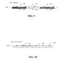
- FIG. 9details a logical block address to physical block address RAM table of a Flash memory of the present invention.
- FIG. 10details an open block identifier RAM table of a Flash memory of the present invention.
- FIG. 11details an open block flags RAM table of a Flash memory of the present invention.
- FIG. 12details an open block count RAM table of a Flash memory of the present invention.
- FIG. 13details a block invalid flags RAM table of a Flash memory of the present invention.
- FIG. 14details a block erased flags RAM table of a Flash memory of the present invention.
- a Flash memory of the present inventionmanages the EBM data in a decentralized approach.
- a Flash memory embodiment of the present inventionincorporates the erase block management information for an individual erase block (EB) in an extended area of the control data section of the first several sectors in the erase block. This allows for single write nonvolatile block updates and block writes. These single write block operations are inherently faster resulting in an improved performance.
- EBindividual erase block
- the distributed EBM data contained in the erase blocksis also inherently load leveling and resistant to write fatigue. If the EBM fields of an erase block are damaged or succumb to write fatigue, only that write block is affected.
- the erase block management system of a Flash memory embodiment of the present inventioncan continue to operate with the EBM information fields in the unaffected erase blocks.
- FIG. 2Shown in FIG. 2 is a simplified diagram of a Flash memory device embodiment of the present invention 200 coupled to a processor 202 with an address 204 , control 206 , and data bus 208 .
- a control state machine 210directs internal operation of the Flash memory device; managing the Flash memory array 212 and updating RAM control registers and tables 214 .
- the Flash memory array 212contains a sequence of erase blocks 216 .
- Each erase block 216contains a series of sectors 218 that contain a user data space 220 and a control data space 222 .
- the control data space 222contains overhead information for operation of the sector 218 , such as an error correction code (not shown) or an erase block management data field area 224 .
- the first six sectors 226 of an erase block 216 of a Flash memory device 200 embodiment of the present inventioncontain erase block management data fields 224 that contain the decentralized erase block management data in their control data space 222 .
- the RAM control registers and tables 214are loaded at power up from the erase block management data fields 224 held in the first six sectors 226 of each erase block 216 by the control state machine 210 .
- the user data space 220 in each sector 218is typically 512 bytes long.
- each erase block 216typically contains 128 sectors 218 and has 6 byte EBM data fields 224 in each sector 218 . It is noted that other formats for the erase blocks 216 and sectors 218 are possible and should be apparent to those skilled in the art with benefit of the present disclosure.
- FIG. 3further details two examples 300 , 302 of the many possible sector formats for a Flash memory erase block of the present invention.
- Both the M42 sector format 300 and the M53 sector format 302contain space for 512 bytes of user data 304 , 306 , 8 bytes of ECC 308 , 310 , and 6 bytes of EBM data 312 , 314 .
- the formatsdiffer, however, in that the M42 sector format 300 contains additional data space for format specific functions 316 , while the M53 sector format 302 does not contain such space.
- Other sector formatsare of course possible and should be apparent to those skilled in the art with the benefit of the present disclosure.
- FIG. 4is shown a diagram of a EBM data field of 6 bytes 400 as would be used in a sector of an erase block of an embodiment of the present invention.
- the EBM data field bytes 0 to 2 , 402contain EBM data.
- the EBM data field bytes 3 to 6 , 404contain the 1s complement of the data in EBM data field bytes 0 to 2 , 402 , for error redundancy purposes.
- an erase block 500 of 128 sectors 508is detailed.
- the erase block management fields of the first six sectors of an erase block of a Flash memory of the present inventionare paired together in 3 groups of 2 sectors each 502 , 504 , 506 . This improves the EBM data redundancy and general fault tolerance of the Flash memory device.
- Each sector 508 of the erase block 500has a 512 byte user data space 510 and a control data space 512 .
- the control data space 512contains an EBM data field of 6 bytes 514 .
- the EBM data fields of the first six sectors 516are utilized in erase block management in a Flash memory device of the present invention.
- sectors 0 and 1are paired 502
- sectors 2 and 3are paired 504
- sectors 4 and 5are paired 506 .
- Identical EBM datais redundantly written to the EBM data fields of each sector in each pair. As long as one sector in the pair can be read the EBM data stored in the sector pair is considered valid. It is noted that other sector EBM data field formats and erase block EBM field arrangements are possible and should be apparent to those skilled in the art with benefit of the present disclosure.
- the erase blockscan have one of four states: “invalid” (unavailable and in need of block erasure), “erased” (available for use), “partially filled” (partially written with user data), and “fully valid” (full of user data).
- FIG. 6shows a table 600 which details the state of an erase block 602 and the contents of the EBM fields 604 of each pair of the first six sectors of the erase block.
- the state of any erase block of an embodiment of the present inventioncan be determined at any time by reading the contents of each pair of the first six sectors of the erase block.
- the erase block management firmware software of a Flash memory device of the present inventionreads these fields for each erase block of the device upon power up and retains the information in the internal RAM tables to improve operation performance.
- the EBM data fields of sectors 0 / 1 606 , sectors 2 / 3 608 , and sectors 4 / 5 610will have an “invalid” pattern written into each sector.
- the invalid pattern for the present embodiment of a Flash memory device of the present inventionis that of all zeros.
- An erase block in the “erased” state 614will have the hexadecimal pattern “AA55AA” and its complement written into sectors 0 / 1 606 .
- the remaining sectors, sectors 2 / 3 608 and sectors 4 / 5 610will be in the “erased” state; which is a pattern of hexadecimal “FFFFFF” for the present embodiment of a Flash memory of the present invention.
- the presence of the “AA55AA” patternis required to indicate the successful completion of the erasure procedure on the erase block.
- the erase blockwill have the hexadecimal pattern “AA55AA” and its complement written into sectors 0 / 1 606 , and sectors 4 / 5 610 will contain a valid block identifier and its complement.
- the block identifierindicates the logical address or address range and type of user data written to the erase block.
- the sectors 2 / 3 608will be in the “erased” state, indicating that the erase block is not closed and that space remains to be written.
- the partially filled stateallows for any number of physical sectors between 0 and 128 to be written.
- the erase blockwill have the hexadecimal pattern “AA55AA” and its complement written into sectors 0 / 1 606 .
- Both sectors 2 / 3 608 and sectors 4 / 5 610will contain a valid block identifiers and their complement.
- the block identifiersindicate the logical address or address range and type of user data written to the erase block.
- the erase blockis considered closed by the EBM control and that no space remains to be written.
- the fully valid stateis an aid to power up initialization, immediately indicating the validity of all sectors of the erase block without further verification.
- LBSLogical Block of Sectors
- Sectors 2 / 3 of the LBS utilized erase blockwill be “erased”, and sectors 0 / 1 will contain the pattern “AA55AA”.
- the erase blockis considered full.
- the LBS utilized erase blockwill then be marked as being the “fully valid” state by having a valid LBS block identifier written into the EBM data fields of both sectors 2 / 3 and sectors 4 / 5 .
- RLSBlock of Repeated Logical Sector Address
- Flash memory deviceAnother such erase block use and block identifier type is the Block of Repeated Logical Sector Address (RLS).
- RLSis designed to be utilized by the Flash memory device to conveniently deal with a sector that is heavily written and rewritten by the host while minimizing write fatigue and the number of time consuming block erasures the Flash memory needs to do.
- the erase blockcontains a single repeated logical sector. When the logical sector is again written by the host it is simply written to the next available physical sector in the erase block. If the RLS utilized erase block is “partially filled”, as described above in the table of FIG. 6 , only sectors 4 / 5 will be written with a valid RLS block identifier in the EBM data field.
- Sectors 2 / 3 of the RLS utilized erase blockwill be “erased”, and sectors 0 / 1 will contain the pattern “AA55AA”. When all the sectors of a RLS utilized erase block have written, the erase block is considered full.
- the RLS utilized erase blockcan be marked as being the “fully valid” state by having a valid RLS block identifier written into the EBM data fields of both sectors 2 / 3 and sectors 4 / 5 . Although, the RLS utilized erase block may be optionally left marked as if in the “partially filled” state for, as state above, the “partially filled” state allows for the sectors between 0 and 128 in an erase block to have been written.
- FIG. 7details the EBM data fields for both a LBS block identifier 700 and a RLS block identifier 702 .
- LBS block identifier 700details the EBM data fields for both a LBS block identifier 700 and a RLS block identifier 702 .
- FIG. 7details the EBM data fields for both a LBS block identifier 700 and a RLS block identifier 702 .
- bytes 0 , 1 , and 2are shown and the is complement versions in bytes 3 , 4 , and 5 are omitted.
- An LBS block identifierindicates the section of 128 contiguous logical sectors stored in this physical erase block. For embodiments of the present invention, this is accomplished by the 12 bit logical block address (LBA) 704 that is written into bytes 1 and 2 of the EBM data field. The remaining 4 bits of EBM data field byte 2 706 are filled with zeros.
- the LBS block identifieralso contains an 8 bit AGE descriptor 708 in byte 0 of the EBM data field, indicating the validity of the data stored in the erase block. As multiple blocks may be identified on the Flash memory device with the same logical block address, this AGE descriptor is utilized by the EBM control to determine the validity of the stored data and retrieve/operate on the most recent.
- An RLS block identifierindicates the logical sector address for the single logical sector of data stored in this physical erase block. As stated above, the same logical sector is written to increasing sector addresses within the erase block. The highest written sector is therefore the most recent data. For this reason there is no “AGE” data for an RLS erase block identifier, for only one will exist for a given logical sector in an RLS utilized erase block at a time.
- An RLS block identifier for embodiments of the present inventioncontains a 19 bit logical sector address 710 written into bytes 0 , 1 , and 2 of the EBM data field. The remaining 5 bits of byte 2 are filled with the bit pattern “00010” 712 . It is noted that other variations of block identifiers are possible and should be apparent to those skilled in the art with the benefit of the present disclosure.
- FIG. 8details an erase block state transition diagram 800 for Flash memory devices of the present invention, showing the “erased” 802 , “invalid” 804 , “partially filled” 806 , and “fully valid” 808 states and their allowed previous and next states. Also detailed are the contents of the EBM data fields of the first six sectors of the erase block when the erase block is in each state. As shown in FIG. 8 , the “erased” state 802 can only be entered from the “invalid” state 804 after a successful erase operation 810 . The “erased” state 802 can then be exited by a transition to the “partially filled” state 806 when data is written to the physical sectors of the erase block 812 .
- the “partially filled” state 806can be exited by either transitioning to the “fully valid” state 808 , by filling the remaining sectors of the erase block 814 , or by transitioning directly to the “invalid” state 804 . Therefore saving overhead by not having to transition through the “fully valid” state 808 first if there is no need to keep the data in the erase block.
- the “fully valid” state 808can be exited by transitioning back to the “invalid” state 804 , when the erase block data is no longer necessary 818 .
- Erase Block Management firmwareutilizes the following RAM data variable structures in control of the erase blocks of an embodiment of the Flash memory device of the present invention: lba_to_pba[lba], open_block_id[index], open_block_flags[index], open_block_count[index], block_invalid_flags[block], block_erased_flags[block].
- the index utilized to access the RAM data structureis shown in brackets in the above listing.
- the lba_to_pba RAM tableshown in FIG. 9 , is a randomly addressable array 900 of 12 bit Physical Block Addresses (PBA) 902 indexed by a logical block address (LBA) value 904 (lba_to_pba[lba]).
- PBAPhysical Block Addresses
- LBAlogical block address
- An entry of 0xFFF in the array 900indicates that the LBA has no corresponding PBA present.
- this tableis initialized to all 0xFFF and filled with LBA to PBA mappings as the EBM data fields are read from the individual erase blocks. In operation, an entry is placed in this table when a physical erase block is transitioned into the “fully valid” state.
- the open_block_id RAM tablecontains the block identifier information (EBM) 1002 and physical block address (PBA) 1004 for all “partially filled” state erase blocks in the Flash memory device as well as an activity indication 1006 for the entry itself.
- EBMblock identifier information
- PBAphysical block address
- Each entryis 6 bytes in size 1000 and accessed by an index value (open_block_id[index]). Entries are ordered by address and age. The most recently updated entry is given an activity value of 0 and all other activity values are incremented. An entry of all ‘FF’s is invalid and power-up initializes this table to invalid entries.
- the open_block_id RAM tableis filled during the initialization with erase blocks in the “partially filled” state as the EBM data fields are read from the individual erase blocks.
- the open_block_flags table 1100contains 128 bit flags 1102 for each “partially filled” erase block of the Flash memory device.
- the tablerepresents each “partially filled” erase block that is present on the Flash memory device or Flash card.
- the open_block_flags tableis accessed by an index value 1104 (open_block_flags[index]).
- a bit flag 1102is set to 1 for each sector in the erase block which contains valid data. This table is initialized to all zeros on power-up and filled as the EBM data fields are read and “partially filled” erase blocks identified and scanned for all sectors that contain valid data.
- the open_block_count table 1200a representation of which shown in FIG. 12 , indicates the number of valid sectors in each “partially filled” erase block on the Flash memory device or Flash card. Each entry is a single byte 1202 and is accessed by an index value 1204 (open_block_count[index]). This table is initialized to all zeros on power-up and filled as the EBM data fields are read and “partially filled” erase blocks identified and scanned for all sectors that contain valid data.
- the block_invalid_flags table 1300contains a bit flag 1302 for each physical erase block on the card.
- the block_invalid_flags tableis accessed by an erase block identifier 1304 (block_invalid_flags[block]).
- a bit flag 1302is set to 1 for each erase block which is in the “invalid” state. This table is initialized to all zeros on power-up and filled as the EBM data fields are read and “invalid” state erase blocks identified.
- the block_erased_flags table 1400shown in FIG. 14 , contains a bit flag 1403 for each physical erase block on the card.
- the block_erased_flags tableis accessed by an erase block identifier 1304 (block_erased_flags[block]).
- a bit flag 1302is set to 1 for each block which is in the “erased” state. This table is initialized to all zeros on power-up and filled as the EBM data fields are read and erase blocks in the “erased” state identified.
- Flash memory RAM tablesare first filled with their power-up default values.
- the state of all erase blocksis then determined and recorded in controller RAM tables by reading the EBM data fields of all erase blocks on the card or Flash memory device to determine each erase block's state and logical block address information.
- the lba_to_pba, open_block_id, block_invalid_flags and block_erased_flags tablesare updated using this information.
- All sectors of each “partially filled” erase block located in the previous sub-processare read to determine the valid state of sectors within the erase block in order to update the open_block_flags and open_block_count tables.
- Read Locationin order to perform a read command and return a written sector data to the host, erase block management control must locate the requested sector data on the Flash memory device.
- the Read Location processwill be given an input start logical sector address (LSA) and a Sector Count from the host.
- LSAlogical sector address
- the Read Location processthen returns with an indication of successful location of data (or not) and, if data is located, a starting Chip, Block and Sector location as well as a Sector Count.
- the returned countwill be equal to or less than the requested count.
- the RAM open_block_id and open_block_flags tablesare first searched for the requested data. Repeated logical sector (RLS) entries are considered by default to be the most recent. Logical blocks of sectors (LBS) entries have the AGE parameter allowing the most recent data to be identified. Entries which locate some of the requested data, but not the first requested sector, force the sector count to be clipped to a value which will exclude sectors in that entry.
- RLSlogical sector
- LBSLogical blocks of sectors
- the erase block management controlin order to perform a write command and write host supplied sector data to the Flash memory device, the erase block management control must allocate the requested erased sector space on the Flash memory.
- the Write Allocation processwill be given an input starting logical sector address (LSA) and a Sector Count from the host.
- LSAlogical sector address
- the Write Allocation processthen returns with an indication of successful allocation of space (or not) and, if space is allocated, a starting Chip, Block and Sector location as well as a Sector Count is returned. The returned count will be equal to or less than the requested count.
- the RAM open_block_id and open_block_flags tablesare initially searched for space in a “partially filled” state erase block for the requested sectors.
- Repeated logical sector (RLS) utilized erase blocksare selected over logical blocks of sectors (LBS) utilized erase blocks by default. If multiple LBS entries are present and applicable to the requested LSA, then only the most recent in AGE is searched. If no space is found for at least the first requested sector in the current “partially filled” state erase blocks, then a new “partially filled” erase block must be opened.
- RLSlogical sector
- LBSlogical blocks of sectors
- a new “partially filled” erase blockis “opened” by first searching the open_block_id table for the correct ordered location and AGE to use for the new entry.
- a physical erase block in the “erased” stateis selected. This information is entered into the correct entry position in the open_block_id table.
- the open_block_flags bits for this entryare set to all zeros and the Activity value of this entry is set to 0.
- the Activity value of all other entriesis incremented, up to a maximum value of 20.
- the selected physical erase block's Partial EBM data field(sectors 4 / 5 ) is written.
- Closing an erase block in the “partially filled” stateis fundamentally the process of removing its entry from the open_block_id table.
- the processes of accomplishing thisare the most complicated in erase block management firmware and differs depending on the type of erase block in the “partially filled” state involved and the number of other erase block in the “partially filled” state open at the time.
- An erase block in the “partially filled” statewith sectors for an LBA which is currently not open in any other erase block, is closed by writing any remaining unwritten sectors using data from any currently existing erase block in the “fully valid” state that contains this data.
- the erase block in the “fully valid” stateis invalidated by programming its EBM data field entries to “invalid”. Its PBA location is then marked in the block_invalid_flags table.
- the “partially filled” erase blockis then marked as in the “fully valid” state through its EBM data field entries and entered into the lba_to_pba table. Finally, the newly closed erase block is removed from the open_block_id table, removing its entry.
- An erase block in the “partially filled” state that contains sectors of an LBA open in other “partially filled” erase blocks, and thus have open_block_id entries,can only be closed if it is the oldest entry (its AGE value is the lowest for that LBA). It is closed by writing any valid sectors in its block for which no valid sectors in younger blocks appear into the youngest block for this LBA.
- the “partially filled” erase blockcan now be invalidated by programming its EBM entries. Its entry in the open_block_id table can then be invalidated.
- a Repeated Logical Sectors (RLS) utilized erase block in the “partially filled” stateis closed by first moving its content of the single most recent data sector it contains into an Logical Block of sectors (LBS) utilized erase block in the “partially filled” state.
- LBSLogical Block of sectors
- the physical RLS utilized erase blockis then invalidated and marked in the block invalid_flags and the entry in the open_block_id table is then removed.
- an erase block in the “erased” stateis selected, for purposes of opening a “partially filled” state erase block, by searching the block_erased_flags table for a non-zero flag bit. For purposes of leveling wear among the erase blocks of the Flash memory device or card, a new search through this table will always begin at the block after the last search completed. This process will return with an indication of success or failure in locating an erased block, and the physical block address located if successful.
- Invalid Block Selectionan erase block in the “invalid” state is selected for erasure by searching the block_invalid_flags table for a non-zero flag bit. For purposes of leveling wear among the Erase Blocks of the Flash memory device or card, a new search through this table will always begin at the block after the last search completed. This process will return with an indication of success or failure in locating an invalid block. The process will return also with the physical block address (PBA) located if successful.
- PBAphysical block address
- EBMdistributed erase block management
- one of the goals of the EBM controlis to minimize write fatigue of the non-volatile floating gate memory cells of the Flash memory device erase blocks by re-mapping and distributing heavily rewritten user data sectors in a process called load leveling so that no one erase block gets overused too quickly and reduce the expected lifespan of the Flash memory device.
- the EBM data structuresare some of the most heavily rewritten non-volatile floating gate memory cells in the device and thus, while helping to reduce write fatigue in the Flash memory device, are some of the data structures most susceptible to the process of fatigue.
- the Flash memory device of the detailed inventioncombines the EBM data in a user data erase block by placing it in an EBM data field of the control data section of the erase block sectors.
- the detailed Flash memoryalso reduces the process of EBM data structure write fatigue by allowing the EBM data fields to be load leveled by rotating them with the erase blocks they describe.
Landscapes
- Engineering & Computer Science (AREA)
- Theoretical Computer Science (AREA)
- Physics & Mathematics (AREA)
- General Engineering & Computer Science (AREA)
- General Physics & Mathematics (AREA)
- Techniques For Improving Reliability Of Storages (AREA)
- Read Only Memory (AREA)
Abstract
Description
Claims (50)
Priority Applications (4)
| Application Number | Priority Date | Filing Date | Title |
|---|---|---|---|
| US09/938,782US6948026B2 (en) | 2001-08-24 | 2001-08-24 | Erase block management |
| US11/199,481US7454558B2 (en) | 2001-08-24 | 2005-08-08 | Non-volatile memory with erase block state indication in data section |
| US12/272,358US8112573B2 (en) | 2001-08-24 | 2008-11-17 | Non-volatile memory with erase block state indication in a subset of sectors of erase block |
| US13/367,012US8433846B2 (en) | 2001-08-24 | 2012-02-06 | Methods and apparatus reading erase block management data in subsets of sectors having user data and control data sections |
Applications Claiming Priority (1)
| Application Number | Priority Date | Filing Date | Title |
|---|---|---|---|
| US09/938,782US6948026B2 (en) | 2001-08-24 | 2001-08-24 | Erase block management |
Related Child Applications (1)
| Application Number | Title | Priority Date | Filing Date |
|---|---|---|---|
| US11/199,481ContinuationUS7454558B2 (en) | 2001-08-24 | 2005-08-08 | Non-volatile memory with erase block state indication in data section |
Publications (2)
| Publication Number | Publication Date |
|---|---|
| US20030041210A1 US20030041210A1 (en) | 2003-02-27 |
| US6948026B2true US6948026B2 (en) | 2005-09-20 |
Family
ID=25471946
Family Applications (4)
| Application Number | Title | Priority Date | Filing Date |
|---|---|---|---|
| US09/938,782Expired - LifetimeUS6948026B2 (en) | 2001-08-24 | 2001-08-24 | Erase block management |
| US11/199,481Expired - LifetimeUS7454558B2 (en) | 2001-08-24 | 2005-08-08 | Non-volatile memory with erase block state indication in data section |
| US12/272,358Expired - Fee RelatedUS8112573B2 (en) | 2001-08-24 | 2008-11-17 | Non-volatile memory with erase block state indication in a subset of sectors of erase block |
| US13/367,012Expired - LifetimeUS8433846B2 (en) | 2001-08-24 | 2012-02-06 | Methods and apparatus reading erase block management data in subsets of sectors having user data and control data sections |
Family Applications After (3)
| Application Number | Title | Priority Date | Filing Date |
|---|---|---|---|
| US11/199,481Expired - LifetimeUS7454558B2 (en) | 2001-08-24 | 2005-08-08 | Non-volatile memory with erase block state indication in data section |
| US12/272,358Expired - Fee RelatedUS8112573B2 (en) | 2001-08-24 | 2008-11-17 | Non-volatile memory with erase block state indication in a subset of sectors of erase block |
| US13/367,012Expired - LifetimeUS8433846B2 (en) | 2001-08-24 | 2012-02-06 | Methods and apparatus reading erase block management data in subsets of sectors having user data and control data sections |
Country Status (1)
| Country | Link |
|---|---|
| US (4) | US6948026B2 (en) |
Cited By (48)
| Publication number | Priority date | Publication date | Assignee | Title |
|---|---|---|---|---|
| US20030135793A1 (en)* | 2002-01-16 | 2003-07-17 | Sandisk Corporation | Method and apparatus for dynamic degradation detection |
| US20030145151A1 (en)* | 2002-01-25 | 2003-07-31 | Hitachi, Ltd. | Nonvolatile memory and memory card |
| US20050132127A1 (en)* | 2003-12-10 | 2005-06-16 | Samsung Electronics Co., Ltd. | Flash memory and mapping control apparatus and method for flash memory |
| US20050188148A1 (en)* | 2004-02-20 | 2005-08-25 | Nec Electronics Corporation | Data access controlling method in flash memory and data access controlling program |
| US20050204115A1 (en)* | 2004-01-30 | 2005-09-15 | Kiminori Matsuno | Semiconductor memory device, memory controller and data recording method |
| US20050273551A1 (en)* | 2001-08-24 | 2005-12-08 | Micron Technology, Inc. | Erase block management |
| US20060224818A1 (en)* | 2005-04-04 | 2006-10-05 | Standard Microsystems Corporation | Method for fast access to flash-memory media |
| US7134025B1 (en) | 2002-03-29 | 2006-11-07 | Xilinx, Inc. | Methods and circuits for preventing the overwriting of memory frames in programmable logic devices |
| US20070168698A1 (en)* | 2005-11-03 | 2007-07-19 | Coulson Richard L | Recovering from a non-volatile memory failure |
| US20080126719A1 (en)* | 2006-11-24 | 2008-05-29 | Radoslav Danilak | System, method, and computer program product for delaying an operation that reduces a lifetime of memory |
| US20080126720A1 (en)* | 2006-11-24 | 2008-05-29 | Radoslav Danilak | Multi-memory device system and method for managing a lifetime thereof |
| US20080126724A1 (en)* | 2006-11-24 | 2008-05-29 | Radoslav Danilak | System, method, and computer program product for reducing memory write operations using difference information |
| US20080126891A1 (en)* | 2006-11-24 | 2008-05-29 | Radoslav Danilak | Memory lifetime gauging system, method and computer program product |
| US20080141054A1 (en)* | 2006-12-08 | 2008-06-12 | Radoslav Danilak | System, method, and computer program product for providing data redundancy in a plurality of storage devices |
| US20080231810A1 (en)* | 2007-03-19 | 2008-09-25 | Catania Louis J | Method of fitting contact lenses |
| US7444579B2 (en) | 2005-04-28 | 2008-10-28 | Micron Technology, Inc. | Non-systematic coded error correction |
| US20080307270A1 (en)* | 2007-06-07 | 2008-12-11 | Micron Technology, Inc. | Emerging bad block detection |
| US20090132778A1 (en)* | 2007-11-19 | 2009-05-21 | Radoslav Danilak | System, method and a computer program product for writing data to different storage devices based on write frequency |
| US20090129163A1 (en)* | 2007-11-19 | 2009-05-21 | Radoslav Danilak | System, method, and computer program product for increasing a lifetime of a plurality of blocks of memory |
| US20100017588A1 (en)* | 2008-07-15 | 2010-01-21 | Radoslav Danilak | System, method, and computer program product for providing an extended capability to a system |
| US20100017566A1 (en)* | 2008-07-15 | 2010-01-21 | Radoslav Danilak | System, method, and computer program product for interfacing computing device hardware of a computing device and an operating system utilizing a virtualization layer |
| US20100064093A1 (en)* | 2008-09-09 | 2010-03-11 | Radoslav Danilak | System, method, and computer program product for converting data in a binary representation to a non-power of two representation |
| US20100146236A1 (en)* | 2008-12-08 | 2010-06-10 | Radoslav Danilak | System, method, and computer program product for rendering at least a portion of data useless in immediate response to a delete command |
| US20100169595A1 (en)* | 2009-01-01 | 2010-07-01 | Sandisk Il Ltd. | Storage backup |
| US20100174847A1 (en)* | 2009-01-05 | 2010-07-08 | Alexander Paley | Non-Volatile Memory and Method With Write Cache Partition Management Methods |
| US20100250830A1 (en)* | 2009-03-27 | 2010-09-30 | Ross John Stenfort | System, method, and computer program product for hardening data stored on a solid state disk |
| US20100251009A1 (en)* | 2009-03-27 | 2010-09-30 | Ross John Stenfort | System, method, and computer program product for converting logical block address de-allocation information in a first format to a second format |
| US20110004710A1 (en)* | 2009-07-06 | 2011-01-06 | Ross John Stenfort | System, method, and computer program product for interfacing one or more storage devices with a plurality of bridge chips |
| US20110004718A1 (en)* | 2009-07-02 | 2011-01-06 | Ross John Stenfort | System, method, and computer program product for ordering a plurality of write commands associated with a storage device |
| US20110016239A1 (en)* | 2009-07-20 | 2011-01-20 | Ross John Stenfort | System, method, and computer program product for reducing a rate of data transfer to at least a portion of memory |
| US20110016233A1 (en)* | 2009-07-17 | 2011-01-20 | Ross John Stenfort | System, method, and computer program product for inserting a gap in information sent from a drive to a host device |
| US7904672B2 (en) | 2006-12-08 | 2011-03-08 | Sandforce, Inc. | System and method for providing data redundancy after reducing memory writes |
| US20110083047A1 (en)* | 2009-10-05 | 2011-04-07 | Ross John Stenfort | System, method, and computer program product for sending failure information from a serial ata (sata) solid state drive (ssd) to a host device |
| US20110145474A1 (en)* | 2009-12-14 | 2011-06-16 | Symwave, Inc. | Efficient Use Of Flash Memory In Flash Drives |
| US8040744B2 (en)* | 2009-01-05 | 2011-10-18 | Sandisk Technologies Inc. | Spare block management of non-volatile memories |
| US8094500B2 (en) | 2009-01-05 | 2012-01-10 | Sandisk Technologies Inc. | Non-volatile memory and method with write cache partitioning |
| US8230159B2 (en) | 2009-03-27 | 2012-07-24 | Lsi Corporation | System, method, and computer program product for sending logical block address de-allocation status information |
| US20120290772A1 (en)* | 2011-05-09 | 2012-11-15 | Canon Kabushiki Kaisha | Storage control apparatus for controlling data writing and deletion to and from semiconductor storage device, and control method and storage medium therefor |
| US8635399B2 (en)* | 2011-10-18 | 2014-01-21 | Stec, Inc. | Reducing a number of close operations on open blocks in a flash memory |
| US8671259B2 (en) | 2009-03-27 | 2014-03-11 | Lsi Corporation | Storage system data hardening |
| US8700840B2 (en) | 2009-01-05 | 2014-04-15 | SanDisk Technologies, Inc. | Nonvolatile memory with write cache having flush/eviction methods |
| US8706990B2 (en) | 2003-10-28 | 2014-04-22 | Sandisk Technologies Inc. | Adaptive internal table backup for non-volatile memory system |
| US20140164824A1 (en)* | 2009-10-27 | 2014-06-12 | Micron Technology, Inc. | Error detection/correction based memory management |
| US9183133B2 (en) | 2007-11-28 | 2015-11-10 | Seagate Technology Llc | System, method, and computer program product for increasing spare space in memory to extend a lifetime of the memory |
| USRE46446E1 (en)* | 2005-05-09 | 2017-06-20 | Sandisk Technologies Llc | Method and system for facilitating fast wake-up of a flash memory system |
| US9766819B2 (en) | 2014-12-30 | 2017-09-19 | Sandisk Technologies Llc | Systems and methods for managing storage endurance |
| CN109119108A (en)* | 2018-08-15 | 2019-01-01 | 杭州阿姆科技有限公司 | A method of improving the Nand service life |
| TWI796148B (en)* | 2022-02-25 | 2023-03-11 | 華邦電子股份有限公司 | Erase method for flash memory |
Families Citing this family (91)
| Publication number | Priority date | Publication date | Assignee | Title |
|---|---|---|---|---|
| TW539946B (en)* | 2001-08-07 | 2003-07-01 | Solid State System Company Ltd | Window-based flash memory storage system, and the management method and the access method thereof |
| GB0123415D0 (en)* | 2001-09-28 | 2001-11-21 | Memquest Ltd | Method of writing data to non-volatile memory |
| DE60332091D1 (en)* | 2002-01-31 | 2010-05-27 | Panasonic Corp | INFORMATION PROCESSING DEVICE, MEMORY MANAGEMENT DEVICE, MEMORY MANAGEMENT PROCESS AND INFORMATION PROCESSING METHOD |
| US20040083334A1 (en)* | 2002-10-28 | 2004-04-29 | Sandisk Corporation | Method and apparatus for managing the integrity of data in non-volatile memory system |
| US6944063B2 (en)* | 2003-01-28 | 2005-09-13 | Sandisk Corporation | Non-volatile semiconductor memory with large erase blocks storing cycle counts |
| US6906961B2 (en) | 2003-06-24 | 2005-06-14 | Micron Technology, Inc. | Erase block data splitting |
| US7321951B2 (en)* | 2003-11-17 | 2008-01-22 | Micron Technology, Inc. | Method for testing flash memory power loss recovery |
| US7480760B2 (en) | 2003-12-17 | 2009-01-20 | Wegener Communications, Inc. | Rotational use of memory to minimize write cycles |
| US7350044B2 (en)* | 2004-01-30 | 2008-03-25 | Micron Technology, Inc. | Data move method and apparatus |
| US7322002B2 (en)* | 2004-05-26 | 2008-01-22 | Micron Technology, Inc. | Erasure pointer error correction |
| US8082382B2 (en)* | 2004-06-04 | 2011-12-20 | Micron Technology, Inc. | Memory device with user configurable density/performance |
| US7398348B2 (en)* | 2004-08-24 | 2008-07-08 | Sandisk 3D Llc | Method and apparatus for using a one-time or few-time programmable memory with a host device designed for erasable/rewritable memory |
| JP3942612B2 (en)* | 2004-09-10 | 2007-07-11 | 東京エレクトロンデバイス株式会社 | Storage device, memory management method, and program |
| JP2006085596A (en)* | 2004-09-17 | 2006-03-30 | Mitsubishi Electric Corp | Information recording / reading device |
| KR100703727B1 (en)* | 2005-01-12 | 2007-04-05 | 삼성전자주식회사 | Non-volatile memory, mapping control device and method therefor |
| US20060277359A1 (en)* | 2005-06-06 | 2006-12-07 | Faber Robert W | Blank memory location detection mechanism |
| US7453723B2 (en)* | 2006-03-01 | 2008-11-18 | Micron Technology, Inc. | Memory with weighted multi-page read |
| FI20060427L (en)* | 2006-05-03 | 2007-11-04 | Tellabs Oy | Method and apparatus for processing a sequential file |
| US7369434B2 (en)* | 2006-08-14 | 2008-05-06 | Micron Technology, Inc. | Flash memory with multi-bit read |
| KR100843133B1 (en)* | 2006-09-20 | 2008-07-02 | 삼성전자주식회사 | Apparatus and Method for Reconstructing Mapping Information from Flash Memory |
| US20080320253A1 (en)* | 2007-06-19 | 2008-12-25 | Andrew Tomlin | Memory device with circuitry for writing data of an atomic transaction |
| US8266391B2 (en)* | 2007-06-19 | 2012-09-11 | SanDisk Technologies, Inc. | Method for writing data of an atomic transaction to a memory device |
| CN101162449B (en)* | 2007-10-08 | 2010-06-02 | 福州瑞芯微电子有限公司 | NAND FLASH controller and data interactive method with NAND FLASH chip |
| US20090164745A1 (en)* | 2007-12-21 | 2009-06-25 | Alan Sinclair | System and Method for Controlling an Amount of Unprogrammed Capacity in Memory Blocks of a Mass Storage System |
| US8775758B2 (en)* | 2007-12-28 | 2014-07-08 | Sandisk Technologies Inc. | Memory device and method for performing a write-abort-safe firmware update |
| JP4536785B2 (en)* | 2008-02-01 | 2010-09-01 | 富士通株式会社 | Information processing apparatus, control unit for controlling data storage performed in information processing apparatus, and data storage control method |
| US8566505B2 (en)* | 2008-04-15 | 2013-10-22 | SMART Storage Systems, Inc. | Flash management using sequential techniques |
| CN101676882B (en)* | 2008-09-16 | 2013-01-16 | 美光科技公司 | Built-in mapping message of memory device |
| US8046530B2 (en)* | 2008-10-02 | 2011-10-25 | Infineon Technologies Ag | Process and method for erase strategy in solid state disks |
| US8452940B2 (en)* | 2008-12-30 | 2013-05-28 | Sandisk Technologies Inc. | Optimized memory management for random and sequential data writing |
| US7925925B2 (en)* | 2008-12-30 | 2011-04-12 | Intel Corporation | Delta checkpoints for a non-volatile memory indirection table |
| US8205063B2 (en)* | 2008-12-30 | 2012-06-19 | Sandisk Technologies Inc. | Dynamic mapping of logical ranges to write blocks |
| US20100174845A1 (en)* | 2009-01-05 | 2010-07-08 | Sergey Anatolievich Gorobets | Wear Leveling for Non-Volatile Memories: Maintenance of Experience Count and Passive Techniques |
| US20100318719A1 (en)* | 2009-06-12 | 2010-12-16 | Micron Technology, Inc. | Methods, memory controllers and devices for wear leveling a memory |
| US8527697B2 (en)* | 2009-07-20 | 2013-09-03 | Netapp, Inc. | Virtualized data storage in a network computing environment |
| US20110035540A1 (en)* | 2009-08-10 | 2011-02-10 | Adtron, Inc. | Flash blade system architecture and method |
| US20110208898A1 (en)* | 2010-02-23 | 2011-08-25 | Samsung Electronics Co., Ltd. | Storage device, computing system, and data management method |
| US8661193B1 (en)* | 2010-10-29 | 2014-02-25 | Western Digital Technologies, Inc. | Disk drive with partial sector management |
| US9098399B2 (en) | 2011-08-31 | 2015-08-04 | SMART Storage Systems, Inc. | Electronic system with storage management mechanism and method of operation thereof |
| US9021231B2 (en) | 2011-09-02 | 2015-04-28 | SMART Storage Systems, Inc. | Storage control system with write amplification control mechanism and method of operation thereof |
| US9021319B2 (en) | 2011-09-02 | 2015-04-28 | SMART Storage Systems, Inc. | Non-volatile memory management system with load leveling and method of operation thereof |
| US8654619B1 (en) | 2011-09-29 | 2014-02-18 | Western Digital Technologies, Inc. | Method and apparatus for operating a disk drive |
| FR2980905B1 (en)* | 2011-09-29 | 2014-03-14 | Continental Automotive France | METHOD FOR ERASING MEMORIZED INFORMATION IN NON-VOLATILE REINSTRIPTIBLE MEMORY, MEMORY STORAGE MEDIUM AND AUTOMOTIVE VEHICLE CALCULATOR |
| US9239781B2 (en) | 2012-02-07 | 2016-01-19 | SMART Storage Systems, Inc. | Storage control system with erase block mechanism and method of operation thereof |
| CN104272241B (en) | 2012-04-30 | 2017-08-15 | 英派尔科技开发有限公司 | The numerical value for improving the life-span of solid-state storage device is represented |
| US8910017B2 (en) | 2012-07-02 | 2014-12-09 | Sandisk Technologies Inc. | Flash memory with random partition |
| TWI509615B (en)* | 2012-08-03 | 2015-11-21 | Phison Electronics Corp | Data storing method, and memory controller and memory storage apparatus using the same |
| US20140129758A1 (en)* | 2012-11-06 | 2014-05-08 | Spansion Llc | Wear leveling in flash memory devices with trim commands |
| GB2507961A (en) | 2012-11-14 | 2014-05-21 | Ibm | Back-up and restoration of data between volatile and flash memory |
| US9671962B2 (en) | 2012-11-30 | 2017-06-06 | Sandisk Technologies Llc | Storage control system with data management mechanism of parity and method of operation thereof |
| US9123445B2 (en) | 2013-01-22 | 2015-09-01 | SMART Storage Systems, Inc. | Storage control system with data management mechanism and method of operation thereof |
| US9214965B2 (en) | 2013-02-20 | 2015-12-15 | Sandisk Enterprise Ip Llc | Method and system for improving data integrity in non-volatile storage |
| US9329928B2 (en) | 2013-02-20 | 2016-05-03 | Sandisk Enterprise IP LLC. | Bandwidth optimization in a non-volatile memory system |
| US9183137B2 (en) | 2013-02-27 | 2015-11-10 | SMART Storage Systems, Inc. | Storage control system with data management mechanism and method of operation thereof |
| US9043780B2 (en) | 2013-03-27 | 2015-05-26 | SMART Storage Systems, Inc. | Electronic system with system modification control mechanism and method of operation thereof |
| US9170941B2 (en) | 2013-04-05 | 2015-10-27 | Sandisk Enterprises IP LLC | Data hardening in a storage system |
| US10049037B2 (en) | 2013-04-05 | 2018-08-14 | Sandisk Enterprise Ip Llc | Data management in a storage system |
| US9543025B2 (en) | 2013-04-11 | 2017-01-10 | Sandisk Technologies Llc | Storage control system with power-off time estimation mechanism and method of operation thereof |
| US10546648B2 (en) | 2013-04-12 | 2020-01-28 | Sandisk Technologies Llc | Storage control system with data management mechanism and method of operation thereof |
| US9898056B2 (en) | 2013-06-19 | 2018-02-20 | Sandisk Technologies Llc | Electronic assembly with thermal channel and method of manufacture thereof |
| US9244519B1 (en) | 2013-06-25 | 2016-01-26 | Smart Storage Systems. Inc. | Storage system with data transfer rate adjustment for power throttling |
| US9367353B1 (en) | 2013-06-25 | 2016-06-14 | Sandisk Technologies Inc. | Storage control system with power throttling mechanism and method of operation thereof |
| US9146850B2 (en) | 2013-08-01 | 2015-09-29 | SMART Storage Systems, Inc. | Data storage system with dynamic read threshold mechanism and method of operation thereof |
| US9431113B2 (en) | 2013-08-07 | 2016-08-30 | Sandisk Technologies Llc | Data storage system with dynamic erase block grouping mechanism and method of operation thereof |
| US9361222B2 (en) | 2013-08-07 | 2016-06-07 | SMART Storage Systems, Inc. | Electronic system with storage drive life estimation mechanism and method of operation thereof |
| US9448946B2 (en) | 2013-08-07 | 2016-09-20 | Sandisk Technologies Llc | Data storage system with stale data mechanism and method of operation thereof |
| GB2517435A (en) | 2013-08-19 | 2015-02-25 | Ibm | Fast data back-up and restore between volatile and flash memory |
| TWI501242B (en)* | 2013-10-04 | 2015-09-21 | Winbond Electronics Corp | Erase method for flash |
| US9152555B2 (en) | 2013-11-15 | 2015-10-06 | Sandisk Enterprise IP LLC. | Data management with modular erase in a data storage system |
| TWI515737B (en)* | 2013-12-09 | 2016-01-01 | 慧榮科技股份有限公司 | Data storage device and data erasing method |
| KR20150071500A (en)* | 2013-12-18 | 2015-06-26 | 삼성전자주식회사 | Method and Apparatus for Managing Data |
| KR20150138528A (en)* | 2014-05-29 | 2015-12-10 | 삼성전자주식회사 | Storage system based on flash memory and operation method thereof |
| US9613715B2 (en) | 2014-06-16 | 2017-04-04 | Sandisk Technologies Llc | Low-test memory stack for non-volatile storage |
| US9653184B2 (en) | 2014-06-16 | 2017-05-16 | Sandisk Technologies Llc | Non-volatile memory module with physical-to-physical address remapping |
| US9772783B2 (en) | 2014-09-25 | 2017-09-26 | Dropbox, Inc. | Constructing an index to facilitate accessing a closed extent in an append-only storage system |
| US9690823B2 (en) | 2014-09-25 | 2017-06-27 | Dropbox, Inc. | Synchronizing copies of an extent in an append-only storage system |
| US9720607B2 (en)* | 2014-09-25 | 2017-08-01 | Dropbox, Inc. | Append-only storage system supporting open and closed extents |
| US9632715B2 (en) | 2015-08-10 | 2017-04-25 | International Business Machines Corporation | Back-up and restoration of data between volatile and flash memory |
| US10120573B2 (en)* | 2015-09-14 | 2018-11-06 | Microsoft Technology Licensing, Llc. | Modular sequential writing of data to data storage devices |
| WO2017058218A1 (en)* | 2015-09-30 | 2017-04-06 | Hewlett Packard Enterprise Development LP. | Using a memory controller to manage access to a memory based on a memory initialization state indicator |
| US10114743B2 (en) | 2016-04-06 | 2018-10-30 | Sandisk Technologies Inc. | Memory erase management |
| KR102351649B1 (en)* | 2017-06-07 | 2022-01-17 | 삼성전자주식회사 | Storage device and operation method thereof |
| CN107346668B (en)* | 2017-07-12 | 2020-08-21 | 武汉新芯集成电路制造有限公司 | Durability test method |
| CN109408409A (en)* | 2018-10-25 | 2019-03-01 | 江苏华存电子科技有限公司 | A method of promoting random writing efficiency |
| US10877900B1 (en) | 2019-06-26 | 2020-12-29 | Western Digital Technologies, Inc. | Enabling faster and regulated device initialization times |
| US11068165B2 (en) | 2019-06-27 | 2021-07-20 | Western Digital Technologies, Inc. | Non-volatile memory data write management |
| US10922012B1 (en) | 2019-09-03 | 2021-02-16 | Dropbox, Inc. | Fair data scrubbing in a data storage system |
| CN111090542A (en)* | 2019-12-17 | 2020-05-01 | 深圳忆联信息系统有限公司 | Abnormal block identification method and device based on abnormal power failure and computer equipment |
| CN113311989B (en)* | 2020-02-26 | 2023-09-22 | 北京君正集成电路股份有限公司 | Parallel use-based double-piece NAND FLASH bad block management method |
| US11527300B2 (en) | 2020-08-26 | 2022-12-13 | Western Digital Technologies, Inc. | Level dependent error correction code protection in multi-level non-volatile memory |
| US11436083B2 (en) | 2020-09-04 | 2022-09-06 | Western Digital Technologies, Inc. | Data address management in non-volatile memory |
Citations (19)
| Publication number | Priority date | Publication date | Assignee | Title |
|---|---|---|---|---|
| US3576982A (en)* | 1968-12-16 | 1971-05-04 | Ibm | Error tolerant read-only storage system |
| US5608684A (en)* | 1994-10-13 | 1997-03-04 | Hewlett-Packard Company | System and method for RAM power and data backup utilizing a capacitor and ROM |
| US5758325A (en)* | 1995-06-21 | 1998-05-26 | Mark Voting Systems, Inc. | Electronic voting system that automatically returns to proper operating state after power outage |
| US5923827A (en)* | 1993-11-10 | 1999-07-13 | Matsushita Graphic Communication Systems, Inc. | Facsimile apparatus using a memory management device having empty memory block maintenance function |
| US5933847A (en)* | 1995-09-28 | 1999-08-03 | Canon Kabushiki Kaisha | Selecting erase method based on type of power supply for flash EEPROM |
| US5966720A (en)* | 1992-02-20 | 1999-10-12 | Fujitsu Limited | Flash memory accessed using only the logical address |
| US6144607A (en)* | 1997-06-25 | 2000-11-07 | Sony Corporation | Memory management apparatus and memory management method |
| US6209069B1 (en)* | 1998-05-11 | 2001-03-27 | Intel Corporation | Method and apparatus using volatile lock architecture for individual block locking on flash memory |
| US6278654B1 (en) | 2000-06-30 | 2001-08-21 | Micron Technology, Inc. | Active terminate command in synchronous flash memory |
| US20010029565A1 (en)* | 1992-06-22 | 2001-10-11 | Kenichi Kaki | Semiconductor storage device |
| US6304497B1 (en) | 2000-06-30 | 2001-10-16 | Micron Technology, Inc. | Synchronous memory status register |
| US6307779B1 (en) | 2000-07-28 | 2001-10-23 | Micron Technology, Inc. | Method and circuitry for bank tracking in write command sequence |
| US20020013879A1 (en)* | 1998-03-18 | 2002-01-31 | Sang-Wook Han | Flash memory array access method and device |
| US6345333B1 (en)* | 1997-07-07 | 2002-02-05 | Sony Corporation | Method and apparatus for reverse rewriting |
| US20020026566A1 (en)* | 1998-06-08 | 2002-02-28 | Kosaku Awada | Data backup in non-volatile memory |
| US6427186B1 (en)* | 1999-03-30 | 2002-07-30 | Frank (Fong-Long) Lin | Memory, interface system and method for mapping logical block numbers to physical sector numbers in a flash memory, using a master index table and a table of physical sector numbers |
| US6513095B1 (en)* | 1999-05-31 | 2003-01-28 | Sharp Kabushiki Kaisha | File system with assured integrity incorporating semiconductor memory device |
| US6772274B1 (en)* | 2000-09-13 | 2004-08-03 | Lexar Media, Inc. | Flash memory system and method implementing LBA to PBA correlation within flash memory array |
| US6845438B1 (en)* | 1997-08-08 | 2005-01-18 | Kabushiki Kaisha Toshiba | Method for controlling non-volatile semiconductor memory system by using look up table |
Family Cites Families (8)
| Publication number | Priority date | Publication date | Assignee | Title |
|---|---|---|---|---|
| EP0935255A2 (en)* | 1989-04-13 | 1999-08-11 | SanDisk Corporation | Flash EEPROM system |
| US6230233B1 (en)* | 1991-09-13 | 2001-05-08 | Sandisk Corporation | Wear leveling techniques for flash EEPROM systems |
| US5907856A (en)* | 1995-07-31 | 1999-05-25 | Lexar Media, Inc. | Moving sectors within a block of information in a flash memory mass storage architecture |
| US6411546B1 (en)* | 1997-03-31 | 2002-06-25 | Lexar Media, Inc. | Nonvolatile memory using flexible erasing methods and method and system for using same |
| JP3898305B2 (en)* | 1997-10-31 | 2007-03-28 | 富士通株式会社 | Semiconductor storage device, control device and control method for semiconductor storage device |
| US6426893B1 (en)* | 2000-02-17 | 2002-07-30 | Sandisk Corporation | Flash eeprom system with simultaneous multiple data sector programming and storage of physical block characteristics in other designated blocks |
| JP4641338B2 (en)* | 2000-08-29 | 2011-03-02 | ルネサスエレクトロニクス株式会社 | Nonvolatile semiconductor memory device and system |
| US6948026B2 (en)* | 2001-08-24 | 2005-09-20 | Micron Technology, Inc. | Erase block management |
- 2001
- 2001-08-24USUS09/938,782patent/US6948026B2/ennot_activeExpired - Lifetime
- 2005
- 2005-08-08USUS11/199,481patent/US7454558B2/ennot_activeExpired - Lifetime
- 2008
- 2008-11-17USUS12/272,358patent/US8112573B2/ennot_activeExpired - Fee Related
- 2012
- 2012-02-06USUS13/367,012patent/US8433846B2/ennot_activeExpired - Lifetime
Patent Citations (20)
| Publication number | Priority date | Publication date | Assignee | Title |
|---|---|---|---|---|
| US3576982A (en)* | 1968-12-16 | 1971-05-04 | Ibm | Error tolerant read-only storage system |
| US5966720A (en)* | 1992-02-20 | 1999-10-12 | Fujitsu Limited | Flash memory accessed using only the logical address |
| US20010029565A1 (en)* | 1992-06-22 | 2001-10-11 | Kenichi Kaki | Semiconductor storage device |
| US6411404B1 (en)* | 1993-11-10 | 2002-06-25 | Matsushita Graphic Communication Systems, Inc. | Memory management device and communication apparatus comprising said memory management device |
| US5923827A (en)* | 1993-11-10 | 1999-07-13 | Matsushita Graphic Communication Systems, Inc. | Facsimile apparatus using a memory management device having empty memory block maintenance function |
| US5608684A (en)* | 1994-10-13 | 1997-03-04 | Hewlett-Packard Company | System and method for RAM power and data backup utilizing a capacitor and ROM |
| US5758325A (en)* | 1995-06-21 | 1998-05-26 | Mark Voting Systems, Inc. | Electronic voting system that automatically returns to proper operating state after power outage |
| US5933847A (en)* | 1995-09-28 | 1999-08-03 | Canon Kabushiki Kaisha | Selecting erase method based on type of power supply for flash EEPROM |
| US6144607A (en)* | 1997-06-25 | 2000-11-07 | Sony Corporation | Memory management apparatus and memory management method |
| US6345333B1 (en)* | 1997-07-07 | 2002-02-05 | Sony Corporation | Method and apparatus for reverse rewriting |
| US6845438B1 (en)* | 1997-08-08 | 2005-01-18 | Kabushiki Kaisha Toshiba | Method for controlling non-volatile semiconductor memory system by using look up table |
| US20020013879A1 (en)* | 1998-03-18 | 2002-01-31 | Sang-Wook Han | Flash memory array access method and device |
| US6209069B1 (en)* | 1998-05-11 | 2001-03-27 | Intel Corporation | Method and apparatus using volatile lock architecture for individual block locking on flash memory |
| US20020026566A1 (en)* | 1998-06-08 | 2002-02-28 | Kosaku Awada | Data backup in non-volatile memory |
| US6427186B1 (en)* | 1999-03-30 | 2002-07-30 | Frank (Fong-Long) Lin | Memory, interface system and method for mapping logical block numbers to physical sector numbers in a flash memory, using a master index table and a table of physical sector numbers |
| US6513095B1 (en)* | 1999-05-31 | 2003-01-28 | Sharp Kabushiki Kaisha | File system with assured integrity incorporating semiconductor memory device |
| US6304497B1 (en) | 2000-06-30 | 2001-10-16 | Micron Technology, Inc. | Synchronous memory status register |
| US6278654B1 (en) | 2000-06-30 | 2001-08-21 | Micron Technology, Inc. | Active terminate command in synchronous flash memory |
| US6307779B1 (en) | 2000-07-28 | 2001-10-23 | Micron Technology, Inc. | Method and circuitry for bank tracking in write command sequence |
| US6772274B1 (en)* | 2000-09-13 | 2004-08-03 | Lexar Media, Inc. | Flash memory system and method implementing LBA to PBA correlation within flash memory array |
Cited By (98)
| Publication number | Priority date | Publication date | Assignee | Title |
|---|---|---|---|---|
| US7454558B2 (en)* | 2001-08-24 | 2008-11-18 | Micron Technology, Inc. | Non-volatile memory with erase block state indication in data section |
| US8433846B2 (en) | 2001-08-24 | 2013-04-30 | Micron Technology, Inc. | Methods and apparatus reading erase block management data in subsets of sectors having user data and control data sections |
| US20050273551A1 (en)* | 2001-08-24 | 2005-12-08 | Micron Technology, Inc. | Erase block management |
| US20090125670A1 (en)* | 2001-08-24 | 2009-05-14 | Micron Technology, Inc. | Erase block management |
| US8112573B2 (en) | 2001-08-24 | 2012-02-07 | Micron Technology, Inc. | Non-volatile memory with erase block state indication in a subset of sectors of erase block |
| US7246268B2 (en)* | 2002-01-16 | 2007-07-17 | Sandisk Corporation | Method and apparatus for dynamic degradation detection |
| US20030135793A1 (en)* | 2002-01-16 | 2003-07-17 | Sandisk Corporation | Method and apparatus for dynamic degradation detection |
| US20030145151A1 (en)* | 2002-01-25 | 2003-07-31 | Hitachi, Ltd. | Nonvolatile memory and memory card |
| US20060143370A1 (en)* | 2002-01-25 | 2006-06-29 | Renesas Technology Corp. | Nonvolatile memory and memory card |
| US7200235B1 (en) | 2002-03-29 | 2007-04-03 | Xilinx, Inc. | Error-checking and correcting decryption-key memory for programmable logic devices |
| US7389429B1 (en) | 2002-03-29 | 2008-06-17 | Xilinx, Inc. | Self-erasing memory for protecting decryption keys and proprietary configuration data |
| US7219237B1 (en) | 2002-03-29 | 2007-05-15 | Xilinx, Inc. | Read- and write-access control circuits for decryption-key memories on programmable logic devices |
| US7162644B1 (en) | 2002-03-29 | 2007-01-09 | Xilinx, Inc. | Methods and circuits for protecting proprietary configuration data for programmable logic devices |
| US7366306B1 (en)* | 2002-03-29 | 2008-04-29 | Xilinx, Inc. | Programmable logic device that supports secure and non-secure modes of decryption-key access |
| US7373668B1 (en) | 2002-03-29 | 2008-05-13 | Xilinx, Inc. | Methods and circuits for protecting proprietary configuration data for programmable logic devices |
| US7134025B1 (en) | 2002-03-29 | 2006-11-07 | Xilinx, Inc. | Methods and circuits for preventing the overwriting of memory frames in programmable logic devices |
| US8706990B2 (en) | 2003-10-28 | 2014-04-22 | Sandisk Technologies Inc. | Adaptive internal table backup for non-volatile memory system |
| US7287117B2 (en)* | 2003-12-10 | 2007-10-23 | Samsung Electronics Co. Ltd. | Flash memory and mapping control apparatus and method for flash memory |
| US20050132127A1 (en)* | 2003-12-10 | 2005-06-16 | Samsung Electronics Co., Ltd. | Flash memory and mapping control apparatus and method for flash memory |
| US20050204115A1 (en)* | 2004-01-30 | 2005-09-15 | Kiminori Matsuno | Semiconductor memory device, memory controller and data recording method |
| US7590793B2 (en)* | 2004-02-20 | 2009-09-15 | Nec Electronics Corporation | Data access controlling method in flash memory and data access controlling program |
| US20050188148A1 (en)* | 2004-02-20 | 2005-08-25 | Nec Electronics Corporation | Data access controlling method in flash memory and data access controlling program |
| US20060224818A1 (en)* | 2005-04-04 | 2006-10-05 | Standard Microsystems Corporation | Method for fast access to flash-memory media |
| US7849253B2 (en)* | 2005-04-04 | 2010-12-07 | Standard Microsystems Corporation | Method for fast access to flash-memory media |
| US7444579B2 (en) | 2005-04-28 | 2008-10-28 | Micron Technology, Inc. | Non-systematic coded error correction |
| USRE46446E1 (en)* | 2005-05-09 | 2017-06-20 | Sandisk Technologies Llc | Method and system for facilitating fast wake-up of a flash memory system |
| US20070168698A1 (en)* | 2005-11-03 | 2007-07-19 | Coulson Richard L | Recovering from a non-volatile memory failure |
| US7516267B2 (en)* | 2005-11-03 | 2009-04-07 | Intel Corporation | Recovering from a non-volatile memory failure |
| US7904764B2 (en) | 2006-11-24 | 2011-03-08 | Sandforce, Inc. | Memory lifetime gauging system, method and computer program product |
| US7904619B2 (en) | 2006-11-24 | 2011-03-08 | Sandforce, Inc. | System, method, and computer program product for reducing memory write operations using difference information |
| US20110167199A1 (en)* | 2006-11-24 | 2011-07-07 | Sandforce Inc. | Techniques for prolonging a lifetime of memory by controlling operations that affect the lifetime of the memory |
| US20080126724A1 (en)* | 2006-11-24 | 2008-05-29 | Radoslav Danilak | System, method, and computer program product for reducing memory write operations using difference information |
| US20110125956A1 (en)* | 2006-11-24 | 2011-05-26 | Sandforce Inc. | Techniques for multi-memory device lifetime management |
| US8230183B2 (en) | 2006-11-24 | 2012-07-24 | Lsi Corporation | Techniques for prolonging a lifetime of memory by controlling operations that affect the lifetime of the memory |
| US20080126719A1 (en)* | 2006-11-24 | 2008-05-29 | Radoslav Danilak | System, method, and computer program product for delaying an operation that reduces a lifetime of memory |
| US20080126720A1 (en)* | 2006-11-24 | 2008-05-29 | Radoslav Danilak | Multi-memory device system and method for managing a lifetime thereof |
| US7747813B2 (en) | 2006-11-24 | 2010-06-29 | Sandforce, Inc. | Multi-memory device system and method for managing a lifetime thereof |
| US8230164B2 (en) | 2006-11-24 | 2012-07-24 | Lsi Corporation | Techniques for multi-memory device lifetime management |
| US20080126891A1 (en)* | 2006-11-24 | 2008-05-29 | Radoslav Danilak | Memory lifetime gauging system, method and computer program product |
| US7809900B2 (en) | 2006-11-24 | 2010-10-05 | Sandforce, Inc. | System, method, and computer program product for delaying an operation that reduces a lifetime of memory |
| US8402184B2 (en) | 2006-11-24 | 2013-03-19 | Lsi Corporation | Techniques for reducing memory write operations using coalescing memory buffers and difference information |
| US7904672B2 (en) | 2006-12-08 | 2011-03-08 | Sandforce, Inc. | System and method for providing data redundancy after reducing memory writes |
| US8090980B2 (en) | 2006-12-08 | 2012-01-03 | Sandforce, Inc. | System, method, and computer program product for providing data redundancy in a plurality of storage devices |
| US8504783B2 (en) | 2006-12-08 | 2013-08-06 | Lsi Corporation | Techniques for providing data redundancy after reducing memory writes |
| US20080141054A1 (en)* | 2006-12-08 | 2008-06-12 | Radoslav Danilak | System, method, and computer program product for providing data redundancy in a plurality of storage devices |
| US20080231810A1 (en)* | 2007-03-19 | 2008-09-25 | Catania Louis J | Method of fitting contact lenses |
| US9405639B2 (en) | 2007-06-07 | 2016-08-02 | Micron Technology, Inc. | Systems and methods for retrieving data |
| US8930771B2 (en) | 2007-06-07 | 2015-01-06 | Micron Technology, Inc. | Systems and methods for retrieving data |
| US7765426B2 (en) | 2007-06-07 | 2010-07-27 | Micron Technology, Inc. | Emerging bad block detection |
| US20110239061A1 (en)* | 2007-06-07 | 2011-09-29 | Micron Technology, Inc. | Systems and methods for retrieving data |
| US20100287410A1 (en)* | 2007-06-07 | 2010-11-11 | Micron Technology, Inc. | Systems and methods for retrieving data |
| US7954004B2 (en) | 2007-06-07 | 2011-05-31 | Micron Technology, Inc. | Systems and methods for retrieving data |
| US20080307270A1 (en)* | 2007-06-07 | 2008-12-11 | Micron Technology, Inc. | Emerging bad block detection |
| US20090132778A1 (en)* | 2007-11-19 | 2009-05-21 | Radoslav Danilak | System, method and a computer program product for writing data to different storage devices based on write frequency |
| US8339881B2 (en) | 2007-11-19 | 2012-12-25 | Lsi Corporation | Techniques for increasing a lifetime of blocks of memory |
| US7903486B2 (en) | 2007-11-19 | 2011-03-08 | Sandforce, Inc. | System, method, and computer program product for increasing a lifetime of a plurality of blocks of memory |
| US7849275B2 (en) | 2007-11-19 | 2010-12-07 | Sandforce, Inc. | System, method and a computer program product for writing data to different storage devices based on write frequency |
| US8230184B2 (en) | 2007-11-19 | 2012-07-24 | Lsi Corporation | Techniques for writing data to different portions of storage devices based on write frequency |
| US20090129163A1 (en)* | 2007-11-19 | 2009-05-21 | Radoslav Danilak | System, method, and computer program product for increasing a lifetime of a plurality of blocks of memory |
| US10318181B2 (en) | 2007-11-28 | 2019-06-11 | Seagate Technology Llc | System, method, and computer program product for increasing spare space in memory to extend a lifetime of the memory |
| US9183133B2 (en) | 2007-11-28 | 2015-11-10 | Seagate Technology Llc | System, method, and computer program product for increasing spare space in memory to extend a lifetime of the memory |
| US9645750B2 (en) | 2007-11-28 | 2017-05-09 | Seagate Technology Llc | System, method, and computer program product for increasing spare space in memory to extend a lifetime of the memory |
| US20100017566A1 (en)* | 2008-07-15 | 2010-01-21 | Radoslav Danilak | System, method, and computer program product for interfacing computing device hardware of a computing device and an operating system utilizing a virtualization layer |
| US20100017588A1 (en)* | 2008-07-15 | 2010-01-21 | Radoslav Danilak | System, method, and computer program product for providing an extended capability to a system |
| US20100064093A1 (en)* | 2008-09-09 | 2010-03-11 | Radoslav Danilak | System, method, and computer program product for converting data in a binary representation to a non-power of two representation |
| US20100146236A1 (en)* | 2008-12-08 | 2010-06-10 | Radoslav Danilak | System, method, and computer program product for rendering at least a portion of data useless in immediate response to a delete command |
| US8412905B2 (en)* | 2009-01-01 | 2013-04-02 | Sandisk Il Ltd. | Storage system having secondary data store to mirror data |
| US20100169595A1 (en)* | 2009-01-01 | 2010-07-01 | Sandisk Il Ltd. | Storage backup |
| US8244960B2 (en) | 2009-01-05 | 2012-08-14 | Sandisk Technologies Inc. | Non-volatile memory and method with write cache partition management methods |
| US8094500B2 (en) | 2009-01-05 | 2012-01-10 | Sandisk Technologies Inc. | Non-volatile memory and method with write cache partitioning |
| US20100174847A1 (en)* | 2009-01-05 | 2010-07-08 | Alexander Paley | Non-Volatile Memory and Method With Write Cache Partition Management Methods |
| US8040744B2 (en)* | 2009-01-05 | 2011-10-18 | Sandisk Technologies Inc. | Spare block management of non-volatile memories |
| US8700840B2 (en) | 2009-01-05 | 2014-04-15 | SanDisk Technologies, Inc. | Nonvolatile memory with write cache having flush/eviction methods |
| US20100250830A1 (en)* | 2009-03-27 | 2010-09-30 | Ross John Stenfort | System, method, and computer program product for hardening data stored on a solid state disk |
| US8090905B2 (en) | 2009-03-27 | 2012-01-03 | Sandforce, Inc. | System, method, and computer program product for converting logical block address de-allocation information in a first format to a second format |
| US20100251009A1 (en)* | 2009-03-27 | 2010-09-30 | Ross John Stenfort | System, method, and computer program product for converting logical block address de-allocation information in a first format to a second format |
| US8230159B2 (en) | 2009-03-27 | 2012-07-24 | Lsi Corporation | System, method, and computer program product for sending logical block address de-allocation status information |
| US8671259B2 (en) | 2009-03-27 | 2014-03-11 | Lsi Corporation | Storage system data hardening |
| US20110004718A1 (en)* | 2009-07-02 | 2011-01-06 | Ross John Stenfort | System, method, and computer program product for ordering a plurality of write commands associated with a storage device |
| US8930606B2 (en) | 2009-07-02 | 2015-01-06 | Lsi Corporation | Ordering a plurality of write commands associated with a storage device |
| US9792074B2 (en) | 2009-07-06 | 2017-10-17 | Seagate Technology Llc | System, method, and computer program product for interfacing one or more storage devices with a plurality of bridge chips |
| US20110004710A1 (en)* | 2009-07-06 | 2011-01-06 | Ross John Stenfort | System, method, and computer program product for interfacing one or more storage devices with a plurality of bridge chips |
| US20110016233A1 (en)* | 2009-07-17 | 2011-01-20 | Ross John Stenfort | System, method, and computer program product for inserting a gap in information sent from a drive to a host device |
| US8140712B2 (en) | 2009-07-17 | 2012-03-20 | Sandforce, Inc. | System, method, and computer program product for inserting a gap in information sent from a drive to a host device |
| US20110016239A1 (en)* | 2009-07-20 | 2011-01-20 | Ross John Stenfort | System, method, and computer program product for reducing a rate of data transfer to at least a portion of memory |
| US8516166B2 (en) | 2009-07-20 | 2013-08-20 | Lsi Corporation | System, method, and computer program product for reducing a rate of data transfer to at least a portion of memory |
| US8108737B2 (en) | 2009-10-05 | 2012-01-31 | Sandforce, Inc. | System, method, and computer program product for sending failure information from a serial ATA (SATA) solid state drive (SSD) to a host device |
| US20110083047A1 (en)* | 2009-10-05 | 2011-04-07 | Ross John Stenfort | System, method, and computer program product for sending failure information from a serial ata (sata) solid state drive (ssd) to a host device |
| US9483370B2 (en)* | 2009-10-27 | 2016-11-01 | Micron Technology, Inc. | Error detection/correction based memory management |
| US20140164824A1 (en)* | 2009-10-27 | 2014-06-12 | Micron Technology, Inc. | Error detection/correction based memory management |
| US20110145474A1 (en)* | 2009-12-14 | 2011-06-16 | Symwave, Inc. | Efficient Use Of Flash Memory In Flash Drives |
| US8489803B2 (en) | 2009-12-14 | 2013-07-16 | Smsc Holdings S.A.R.L. | Efficient use of flash memory in flash drives |
| US20120290772A1 (en)* | 2011-05-09 | 2012-11-15 | Canon Kabushiki Kaisha | Storage control apparatus for controlling data writing and deletion to and from semiconductor storage device, and control method and storage medium therefor |
| US8635399B2 (en)* | 2011-10-18 | 2014-01-21 | Stec, Inc. | Reducing a number of close operations on open blocks in a flash memory |
| US9766819B2 (en) | 2014-12-30 | 2017-09-19 | Sandisk Technologies Llc | Systems and methods for managing storage endurance |
| US10268396B2 (en) | 2014-12-30 | 2019-04-23 | Sandisk Technologies Llc | Systems and methods for managing storage endurance |
| CN109119108A (en)* | 2018-08-15 | 2019-01-01 | 杭州阿姆科技有限公司 | A method of improving the Nand service life |
| TWI796148B (en)* | 2022-02-25 | 2023-03-11 | 華邦電子股份有限公司 | Erase method for flash memory |
Also Published As
| Publication number | Publication date |
|---|---|
| US20050273551A1 (en) | 2005-12-08 |
| US20120137056A1 (en) | 2012-05-31 |
| US8112573B2 (en) | 2012-02-07 |
| US7454558B2 (en) | 2008-11-18 |
| US20090125670A1 (en) | 2009-05-14 |
| US8433846B2 (en) | 2013-04-30 |
| US20030041210A1 (en) | 2003-02-27 |
Similar Documents
| Publication | Publication Date | Title |
|---|---|---|
| US6948026B2 (en) | Erase block management | |
| US9489301B2 (en) | Memory systems | |
| US6381176B1 (en) | Method of driving remapping in flash memory and flash memory architecture suitable therefor | |
| US8041884B2 (en) | Controller for non-volatile memories and methods of operating the memory controller | |
| KR100292011B1 (en) | Flash file means | |
| US6865658B2 (en) | Nonvolatile data management system using data segments and link information | |
| US7193899B2 (en) | Erase block data splitting | |
| US7277978B2 (en) | Runtime flash device detection and configuration for flash data management software | |
| EP1410399B1 (en) | Method and apparatus for decreasing block write operation times performed on nonvolatile memory | |
| US5479638A (en) | Flash memory mass storage architecture incorporation wear leveling technique | |
| US7389397B2 (en) | Method of storing control information in a large-page flash memory device | |
| US20110231597A1 (en) | Data access method, memory controller and memory storage system | |
| JP2007280428A (en) | Memory management | |
| GB2411499A (en) | Maintaining erased blocks in a non-volatile memory | |
| JP2021068129A (en) | Memory controller and flash memory system | |
| WO2006093304A1 (en) | Storage device, memory block managing method, and program |
Legal Events
| Date | Code | Title | Description |
|---|---|---|---|
| AS | Assignment | Owner name:MICRON TECHNOLOGY, INC., IDAHO Free format text:ASSIGNMENT OF ASSIGNORS INTEREST;ASSIGNOR:KEAYS, BRADY L.;REEL/FRAME:012121/0164 Effective date:20010817 | |
| FEPP | Fee payment procedure | Free format text:PAYOR NUMBER ASSIGNED (ORIGINAL EVENT CODE: ASPN); ENTITY STATUS OF PATENT OWNER: LARGE ENTITY | |
| STCF | Information on status: patent grant | Free format text:PATENTED CASE | |
| CC | Certificate of correction | ||
| FPAY | Fee payment | Year of fee payment:4 | |
| FPAY | Fee payment | Year of fee payment:8 | |
| AS | Assignment | Owner name:U.S. BANK NATIONAL ASSOCIATION, AS COLLATERAL AGENT, CALIFORNIA Free format text:SECURITY INTEREST;ASSIGNOR:MICRON TECHNOLOGY, INC.;REEL/FRAME:038669/0001 Effective date:20160426 Owner name:U.S. BANK NATIONAL ASSOCIATION, AS COLLATERAL AGEN Free format text:SECURITY INTEREST;ASSIGNOR:MICRON TECHNOLOGY, INC.;REEL/FRAME:038669/0001 Effective date:20160426 | |
| AS | Assignment | Owner name:MORGAN STANLEY SENIOR FUNDING, INC., AS COLLATERAL AGENT, MARYLAND Free format text:PATENT SECURITY AGREEMENT;ASSIGNOR:MICRON TECHNOLOGY, INC.;REEL/FRAME:038954/0001 Effective date:20160426 Owner name:MORGAN STANLEY SENIOR FUNDING, INC., AS COLLATERAL Free format text:PATENT SECURITY AGREEMENT;ASSIGNOR:MICRON TECHNOLOGY, INC.;REEL/FRAME:038954/0001 Effective date:20160426 | |
| FPAY | Fee payment | Year of fee payment:12 | |
| AS | Assignment | Owner name:U.S. BANK NATIONAL ASSOCIATION, AS COLLATERAL AGENT, CALIFORNIA Free format text:CORRECTIVE ASSIGNMENT TO CORRECT THE REPLACE ERRONEOUSLY FILED PATENT #7358718 WITH THE CORRECT PATENT #7358178 PREVIOUSLY RECORDED ON REEL 038669 FRAME 0001. ASSIGNOR(S) HEREBY CONFIRMS THE SECURITY INTEREST;ASSIGNOR:MICRON TECHNOLOGY, INC.;REEL/FRAME:043079/0001 Effective date:20160426 Owner name:U.S. BANK NATIONAL ASSOCIATION, AS COLLATERAL AGEN Free format text:CORRECTIVE ASSIGNMENT TO CORRECT THE REPLACE ERRONEOUSLY FILED PATENT #7358718 WITH THE CORRECT PATENT #7358178 PREVIOUSLY RECORDED ON REEL 038669 FRAME 0001. ASSIGNOR(S) HEREBY CONFIRMS THE SECURITY INTEREST;ASSIGNOR:MICRON TECHNOLOGY, INC.;REEL/FRAME:043079/0001 Effective date:20160426 | |
| AS | Assignment | Owner name:JPMORGAN CHASE BANK, N.A., AS COLLATERAL AGENT, ILLINOIS Free format text:SECURITY INTEREST;ASSIGNORS:MICRON TECHNOLOGY, INC.;MICRON SEMICONDUCTOR PRODUCTS, INC.;REEL/FRAME:047540/0001 Effective date:20180703 Owner name:JPMORGAN CHASE BANK, N.A., AS COLLATERAL AGENT, IL Free format text:SECURITY INTEREST;ASSIGNORS:MICRON TECHNOLOGY, INC.;MICRON SEMICONDUCTOR PRODUCTS, INC.;REEL/FRAME:047540/0001 Effective date:20180703 | |
| AS | Assignment | Owner name:MICRON TECHNOLOGY, INC., IDAHO Free format text:RELEASE BY SECURED PARTY;ASSIGNOR:U.S. BANK NATIONAL ASSOCIATION, AS COLLATERAL AGENT;REEL/FRAME:047243/0001 Effective date:20180629 | |
| AS | Assignment | Owner name:MICRON TECHNOLOGY, INC., IDAHO Free format text:RELEASE BY SECURED PARTY;ASSIGNOR:MORGAN STANLEY SENIOR FUNDING, INC., AS COLLATERAL AGENT;REEL/FRAME:050937/0001 Effective date:20190731 | |
| AS | Assignment | Owner name:MICRON SEMICONDUCTOR PRODUCTS, INC., IDAHO Free format text:RELEASE BY SECURED PARTY;ASSIGNOR:JPMORGAN CHASE BANK, N.A., AS COLLATERAL AGENT;REEL/FRAME:051028/0001 Effective date:20190731 Owner name:MICRON TECHNOLOGY, INC., IDAHO Free format text:RELEASE BY SECURED PARTY;ASSIGNOR:JPMORGAN CHASE BANK, N.A., AS COLLATERAL AGENT;REEL/FRAME:051028/0001 Effective date:20190731 |