US6947639B2 - Integrated polarization coupler - Google Patents
Integrated polarization couplerDownload PDFInfo
- Publication number
- US6947639B2 US6947639B2US10/298,465US29846502AUS6947639B2US 6947639 B2US6947639 B2US 6947639B2US 29846502 AUS29846502 AUS 29846502AUS 6947639 B2US6947639 B2US 6947639B2
- Authority
- US
- United States
- Prior art keywords
- waveguide
- stress
- substrate
- polarization
- strip
- Prior art date
- Legal status (The legal status is an assumption and is not a legal conclusion. Google has not performed a legal analysis and makes no representation as to the accuracy of the status listed.)
- Expired - Fee Related, expires
Links
- 230000010287polarizationEffects0.000titleclaimsabstractdescription130
- 239000000758substrateSubstances0.000claimsabstractdescription77
- 230000003287optical effectEffects0.000claimsabstractdescription39
- 238000010168coupling processMethods0.000claimsabstractdescription35
- 238000005859coupling reactionMethods0.000claimsabstractdescription35
- 230000008878couplingEffects0.000claimsabstractdescription34
- 230000001939inductive effectEffects0.000claimsabstractdescription26
- 238000004891communicationMethods0.000claimsabstractdescription13
- 238000000034methodMethods0.000claimsdescription19
- 239000000463materialSubstances0.000claimsdescription18
- 230000004044responseEffects0.000claimsdescription5
- 230000031070response to heatEffects0.000claims2
- 230000001902propagating effectEffects0.000description22
- 239000013598vectorSubstances0.000description14
- VYPSYNLAJGMNEJ-UHFFFAOYSA-NSilicium dioxideChemical compoundO=[Si]=OVYPSYNLAJGMNEJ-UHFFFAOYSA-N0.000description6
- 230000003321amplificationEffects0.000description6
- 238000003199nucleic acid amplification methodMethods0.000description6
- 238000001069Raman spectroscopyMethods0.000description5
- 239000011521glassSubstances0.000description5
- 239000002184metalSubstances0.000description5
- 229910052751metalInorganic materials0.000description5
- 229910052796boronInorganic materials0.000description4
- 230000008859changeEffects0.000description4
- 238000009826distributionMethods0.000description4
- ZOXJGFHDIHLPTG-UHFFFAOYSA-NBoronChemical compound[B]ZOXJGFHDIHLPTG-UHFFFAOYSA-N0.000description3
- 239000000203mixtureSubstances0.000description3
- 229920000642polymerPolymers0.000description3
- 239000000377silicon dioxideSubstances0.000description3
- 238000000151depositionMethods0.000description2
- 238000001514detection methodMethods0.000description2
- 238000005530etchingMethods0.000description2
- 239000000835fiberSubstances0.000description2
- 238000010438heat treatmentMethods0.000description2
- 150000002739metalsChemical class0.000description2
- 230000008569processEffects0.000description2
- 229910052710siliconInorganic materials0.000description2
- 239000010703siliconSubstances0.000description2
- 238000012546transferMethods0.000description2
- 230000015572biosynthetic processEffects0.000description1
- 230000006835compressionEffects0.000description1
- 238000007906compressionMethods0.000description1
- 239000000470constituentSubstances0.000description1
- 238000010276constructionMethods0.000description1
- 238000001816coolingMethods0.000description1
- 238000001312dry etchingMethods0.000description1
- 230000000694effectsEffects0.000description1
- 239000002305electric materialSubstances0.000description1
- 238000005516engineering processMethods0.000description1
- 239000000284extractSubstances0.000description1
- 238000007710freezingMethods0.000description1
- 230000008014freezingEffects0.000description1
- 238000005286illuminationMethods0.000description1
- 238000003384imaging methodMethods0.000description1
- 238000009616inductively coupled plasmaMethods0.000description1
- 238000004519manufacturing processMethods0.000description1
- 238000005259measurementMethods0.000description1
- 230000000737periodic effectEffects0.000description1
- 230000003094perturbing effectEffects0.000description1
- 238000001020plasma etchingMethods0.000description1
- 238000001228spectrumMethods0.000description1
- 238000012360testing methodMethods0.000description1
- 238000001039wet etchingMethods0.000description1
Images


Classifications
- G—PHYSICS
- G02—OPTICS
- G02B—OPTICAL ELEMENTS, SYSTEMS OR APPARATUS
- G02B6/00—Light guides; Structural details of arrangements comprising light guides and other optical elements, e.g. couplings
- G02B6/10—Light guides; Structural details of arrangements comprising light guides and other optical elements, e.g. couplings of the optical waveguide type
- G02B6/12—Light guides; Structural details of arrangements comprising light guides and other optical elements, e.g. couplings of the optical waveguide type of the integrated circuit kind
- G02B6/126—Light guides; Structural details of arrangements comprising light guides and other optical elements, e.g. couplings of the optical waveguide type of the integrated circuit kind using polarisation effects
- G—PHYSICS
- G02—OPTICS
- G02B—OPTICAL ELEMENTS, SYSTEMS OR APPARATUS
- G02B6/00—Light guides; Structural details of arrangements comprising light guides and other optical elements, e.g. couplings
- G02B6/10—Light guides; Structural details of arrangements comprising light guides and other optical elements, e.g. couplings of the optical waveguide type
- G02B6/12—Light guides; Structural details of arrangements comprising light guides and other optical elements, e.g. couplings of the optical waveguide type of the integrated circuit kind
- G02B6/12007—Light guides; Structural details of arrangements comprising light guides and other optical elements, e.g. couplings of the optical waveguide type of the integrated circuit kind forming wavelength selective elements, e.g. multiplexer, demultiplexer
- G—PHYSICS
- G02—OPTICS
- G02B—OPTICAL ELEMENTS, SYSTEMS OR APPARATUS
- G02B6/00—Light guides; Structural details of arrangements comprising light guides and other optical elements, e.g. couplings
- G02B6/10—Light guides; Structural details of arrangements comprising light guides and other optical elements, e.g. couplings of the optical waveguide type
- G02B6/12—Light guides; Structural details of arrangements comprising light guides and other optical elements, e.g. couplings of the optical waveguide type of the integrated circuit kind
- G02B6/122—Basic optical elements, e.g. light-guiding paths
- G02B6/124—Geodesic lenses or integrated gratings
- G—PHYSICS
- G02—OPTICS
- G02B—OPTICAL ELEMENTS, SYSTEMS OR APPARATUS
- G02B6/00—Light guides; Structural details of arrangements comprising light guides and other optical elements, e.g. couplings
- G02B6/24—Coupling light guides
- G02B6/42—Coupling light guides with opto-electronic elements
- G—PHYSICS
- G02—OPTICS
- G02F—OPTICAL DEVICES OR ARRANGEMENTS FOR THE CONTROL OF LIGHT BY MODIFICATION OF THE OPTICAL PROPERTIES OF THE MEDIA OF THE ELEMENTS INVOLVED THEREIN; NON-LINEAR OPTICS; FREQUENCY-CHANGING OF LIGHT; OPTICAL LOGIC ELEMENTS; OPTICAL ANALOGUE/DIGITAL CONVERTERS
- G02F1/00—Devices or arrangements for the control of the intensity, colour, phase, polarisation or direction of light arriving from an independent light source, e.g. switching, gating or modulating; Non-linear optics
- G02F1/01—Devices or arrangements for the control of the intensity, colour, phase, polarisation or direction of light arriving from an independent light source, e.g. switching, gating or modulating; Non-linear optics for the control of the intensity, phase, polarisation or colour
- G02F1/0128—Devices or arrangements for the control of the intensity, colour, phase, polarisation or direction of light arriving from an independent light source, e.g. switching, gating or modulating; Non-linear optics for the control of the intensity, phase, polarisation or colour based on electro-mechanical, magneto-mechanical, elasto-optic effects
- G02F1/0131—Devices or arrangements for the control of the intensity, colour, phase, polarisation or direction of light arriving from an independent light source, e.g. switching, gating or modulating; Non-linear optics for the control of the intensity, phase, polarisation or colour based on electro-mechanical, magneto-mechanical, elasto-optic effects based on photo-elastic effects, e.g. mechanically induced birefringence
- G02F1/0134—Devices or arrangements for the control of the intensity, colour, phase, polarisation or direction of light arriving from an independent light source, e.g. switching, gating or modulating; Non-linear optics for the control of the intensity, phase, polarisation or colour based on electro-mechanical, magneto-mechanical, elasto-optic effects based on photo-elastic effects, e.g. mechanically induced birefringence in optical waveguides
- G—PHYSICS
- G02—OPTICS
- G02F—OPTICAL DEVICES OR ARRANGEMENTS FOR THE CONTROL OF LIGHT BY MODIFICATION OF THE OPTICAL PROPERTIES OF THE MEDIA OF THE ELEMENTS INVOLVED THEREIN; NON-LINEAR OPTICS; FREQUENCY-CHANGING OF LIGHT; OPTICAL LOGIC ELEMENTS; OPTICAL ANALOGUE/DIGITAL CONVERTERS
- G02F2202/00—Materials and properties
- G02F2202/40—Materials having a particular birefringence, retardation
- G—PHYSICS
- G02—OPTICS
- G02F—OPTICAL DEVICES OR ARRANGEMENTS FOR THE CONTROL OF LIGHT BY MODIFICATION OF THE OPTICAL PROPERTIES OF THE MEDIA OF THE ELEMENTS INVOLVED THEREIN; NON-LINEAR OPTICS; FREQUENCY-CHANGING OF LIGHT; OPTICAL LOGIC ELEMENTS; OPTICAL ANALOGUE/DIGITAL CONVERTERS
- G02F2203/00—Function characteristic
- G02F2203/06—Polarisation independent
- G—PHYSICS
- G02—OPTICS
- G02F—OPTICAL DEVICES OR ARRANGEMENTS FOR THE CONTROL OF LIGHT BY MODIFICATION OF THE OPTICAL PROPERTIES OF THE MEDIA OF THE ELEMENTS INVOLVED THEREIN; NON-LINEAR OPTICS; FREQUENCY-CHANGING OF LIGHT; OPTICAL LOGIC ELEMENTS; OPTICAL ANALOGUE/DIGITAL CONVERTERS
- G02F2203/00—Function characteristic
- G02F2203/58—Multi-wavelength, e.g. operation of the device at a plurality of wavelengths
Definitions
- the inventionrelates to integrated optical devices, and in particular, to polarization couplers.
- a known method for amplifying an optical signal beam propagating in a waveguideis to pass a pump beam through the same waveguide.
- the pump beamtransfers energy to phonons within the waveguide. If the wavelength of the pump beam is correctly chosen, the energy in these phonons is transferred to the signal beam, thus amplifying the optical signal.
- the optical signaloccupies a band of wavelengths.
- a single pump beamcan only amplify a limited portion of the entire band occupied by the optical signal.
- the extent to which a pump beam amplifies the signal beamalso depends on the polarization difference between the pump beam and the signal beam.
- the pump beamhaving been generated by a nearby laser, is typically linearly polarized.
- the signal beamhaving been generated far away, has become thoroughly depolarized.
- the amplification of the signal beamwill depend on whether the linearly-polarized pump beam and the randomly polarized signal beam happen to share the same polarization.
- the inventionincludes a polarization coupler in which a stress-inducing feature is disposed to generate a stress-field in a substrate.
- First and second waveguides, each having a coupling portion,pass through the stress-field.
- First and second periodic-structuresare in optical communication with the coupling portions of the first and second waveguides.
- the first periodic-structureincludes a grating.
- This gratingcan be a short-period grating or a long-period grating.
- the first and second periodic-structuresare either aligned with each other or are offset from one another.
- the offset between the first and second periodic-structurescan be along the axial dimension of the waveguide or a transverse dimension.
- a stress-inducing featureis a stress-inducing strip disposed on the surface of the substrate. Such a stress-inducing strip can be placed above the first waveguide or it can extend across the first and second waveguides.
- One way to generate a stress-fieldis to select a strip material having a coefficient of thermal expansion that differs from a coefficient of thermal expansion of the substrate.
- the first and second waveguideshave first and second cross-sections respectively.
- the first and second cross-sectionsare the same.
- the inventionalso includes those embodiments in which the first and second cross-sections are different from each other.
- the inventionin another aspect, includes an integrated optical circuit on a substrate having a birefringent portion.
- First and second waveguides having respective first-waveguide and second-waveguide coupling sectionspass through the birefringent portion.
- a first-waveguide periodic-structureis in optical communication with the first-waveguide coupling-portion and a second-waveguide periodic-structure is in optical communication with the second-waveguide coupling-portion.
- Another aspect of the inventionis a method for combining a first light wave having a first polarization and a second light wave having a second polarization.
- the methodincludes inducing a stress field in a substrate and guiding the first and second light waves through the stress field in respective first and second waveguides.
- the first and second waveguideseach have a coupling portion in optical communication with a corresponding periodic-structure.
- the polarization couplercan be integrated into a substrate and can therefore be easily manufactured using conventional process steps.
- FIGS. 1-4show embodiments of a wavelength polarization multiplexer.
- FIGS. 5-6show a polarization rotator used in one of the wavelength polarization multiplexers of FIGS. 1-4 .
- FIGS. 7-9show plan, perspective and cross-sectional views respectively of a polarization coupler that can be used in any of the wavelength polarization multiplexers of FIGS. 1-4 .
- FIGS. 10-11show alternative arrangements for a polarization coupler structure.
- FIGS. 12-13show alternative stress-inducing structures.
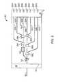
- FIG. 1shows a first embodiment 8 A of an optical multiplexer that combines several beams having different wavelengths and polarizations into one output beam.
- the first embodiment 8 Aincludes a planar substrate 10 having an input 12 adjoining an input coupling region 14 and an output 16 adjoining an output coupling region 18 .
- a plurality of laser diode pairs 20 A-B, 20 C-D, 20 E-F, 20 G-Hcouple their light energy to corresponding inputs in the input coupling region 14 .
- first and second laser diodes 20 A-Bwhich emit light at the same wavelength with the same polarization (herein referred to as the “principal polarization”), pass first and second beams into the input coupling region 14 .
- Each laser diode pair 20 A-Bemits light at a wavelength that differs from the wavelengths emitted by other laser diode pairs 20 C-D, 20 E-F, 20 G-H.
- the number of laser diode pairs, and hence the number of wavelengths propagating within the optical multiplexer,can be varied to suit the application of the optical multiplexer.
- the first beamis coupled into a first waveguide 22 A that extends from the input 12 to the output face 16 .
- the second beamis coupled into a second waveguide 22 B that extends from the input 12 to a first polarization coupler 24 A proximate to the first waveguide 22 A.
- the first and second beamsare coupled to the respective first and second waveguides 22 A, 22 B by a lens coupling system (not shown).
- the currents driving each laser diode 20 A-Hare controlled by an external control circuit (not shown).
- the control circuitprovides selected currents to the respective laser diodes 20 A-H to achieve gain flattening across the laser diodes 20 A-H. In doing so, the control circuit relies, to some extent, on a feedback signal indicative of the power output of a particular laser diode.
- a feedback signalcan be obtained by providing a tap 25 that extracts, from a waveguide 22 G, a portion of the energy delivered to that waveguide 22 G by its associated laser diode 20 G.
- polarization rotatorrefers to a two-port device that rotates the polarization of light passing therethrough by a selected angle. Typically, this angle is an odd multiple of ninety degrees, in which case the polarization rotator 26 A transforms a principally polarized beam at its input into an orthogonally polarized beam at its output.
- the first and second laser diodes 20 A-Bare identical in structure and configuration. As a result, the first and second beams are both principally polarized. After passing through the first polarization rotator 26 A, the second beam, which is now orthogonally polarized relative to the first beam, proceeds to the first polarization coupler 24 A. At the first polarization coupler 24 A, the orthogonally polarized second beam is added to the principally polarized first beam already propagating on the first waveguide 22 A.
- polarization couplerrefers to a four-port device integrated into the substrate 10 that combines orthogonally polarized beams presented at its first and second input ports and provides the resulting combined beam at a first output port. A second output port of the polarization coupler terminates in the substrate 10 .
- Third and fourth beams from respective third and fourth laser diodes 20 C-D, both of which emit light at a second wavelength,are coupled to third and fourth waveguides 22 C-D in the same manner described above in connection with the first and second laser diodes 20 A-B.
- the third waveguide 22 Cextends from the input 12 to a first wavelength coupler 28 A proximate to the first waveguide 22 A.
- wavelength couplerrefers to a four-port device integrated into the substrate 10 that combines beams of different wavelengths present at its first and second input ports and provides the resulting combined beam at a first output port. A second output port of the wavelength coupler terminates in the substrate 10 .
- wavelength specific coupling devicessuch as a wavelength coupler, avoids the possibility that beams of other wavelengths that are already propagating on the first waveguide 22 A will leak out through a coupler each time an additional beam is placed on the first waveguide 22 A.
- the third beamis combined with the first and second beams already propagating on the first waveguide 22 A.
- the fourth waveguide 22 Dextends from the input 12 , through a second polarization rotator 26 B, to a second polarization coupler 24 B, as described above in connection with the second waveguide 22 B.
- the fourth beamwhich has a polarization orthogonal to the third beam, is also combined with the beams already propagating on the first waveguide 22 A.
- the first waveguide 22 Anow carries orthogonally polarized beams at the first wavelength and orthogonally polarized beams at the second wavelength.
- fifth and sixth laser diodes 20 E-Femitting fifth and sixth beams at a third wavelength
- seventh and eighth laser diodes 20 G-Hemitting seventh and eighth beams at a fourth wavelength.
- the fifth and seventh beamsare guided to second and third wavelength couplers 28 B-C by fifth and seventh waveguides 22 E, 22 G.
- the fifth and seventh beamsare thus added, with their principal polarizations intact, to the beams already propagating in the first waveguide 22 A.
- sixth and eight beams emitted by sixth and eighth laser diodes 20 F, 20 Hare coupled to sixth and eight waveguides 22 F, 22 H.
- the sixth and eighth waveguides 22 F, 22 Hguide the sixth and eight beams through third and fourth polarization rotators 26 C-D and on to third and fourth polarization couplers 24 C-D.
- the third and fourth polarization couplers 24 C-Dadd the sixth and eighth beams, which have now had their polarizations rotated, to the beams that are already propagating on the first waveguide 22 A.
- the first waveguide 22 Aextends to the output face 16 of the substrate 10 , carrying with it all eight constituent components collected as it traversed the substrate 10 from the input 12 to the output 14 .
- This beamis coupled, across the coupling region 18 , into an output waveguide 30 .
- FIG. 2shows a second embodiment 8 B embodiment for an optical multiplexer.
- the second waveguide 22 Bcollects all four orthogonally polarized beams, which are at four different wavelengths and directs them to a broadband polarization coupler 32 .
- the broadband polarization coupler 32combines these four orthogonally polarized beams with the four principally polarized beams already propagating on the first waveguide 22 A.
- the first waveguide 22 Apasses through first, second, and third wavelength couplers 28 A-C. These wavelength couplers 28 A-C add the third, fifth, and seventh beams, all of which are principally polarized, to the first beam (also principally polarized) already propagating on the first waveguide 22 A.
- the second waveguide 22 Bpasses through three different wavelength couplers 28 D-F. At each of the wavelength couplers the second waveguide 22 B collects a beam of a different wavelength whose polarization has been rotated by a polarization rotator 26 A-D. The second waveguide 22 B carries its collected orthogonally polarized beams into the broadband polarization coupler 32 .
- the broadband polarization coupler 32couples the orthogonally polarized light to the first waveguide 22 A.
- the second embodiment 8 B shown in FIG. 2thus requires only one, albeit broadband, polarization coupler 32 rather than the four narrowband polarization couplers 24 A-D shown in FIG. 1 .
- FIG. 3shows a third embodiment 8 C similar to the second embodiment 8 B shown in FIG. 2 , the principal difference being that the beams collected by the second waveguide 22 B at each wavelength coupler 28 D-F retain their principal polarization.
- the second waveguide 22 Bbrings these collected beams, all of which are at different wavelengths, to a broadband polarization rotator 34 .
- the broadband polarization rotator 34the polarizations of the collected beams are all rotated together.
- the second waveguide 22 Bdirects the now orthogonally polarized beams to the broadband polarization coupler 32 , which places then all at once into the first waveguide 22 A.
- the embodiment shown in FIG. 3requires only a single polarization coupler 32 . However, it also requires only a single, albeit broadband, polarization rotator 34 instead of the four narrowband polarization rotators 26 A-D shown in FIGS. 1 and 2 .
- FIG. 4shows a fourth embodiment 8 D that, like the first embodiment 8 A, relies on four narrowband polarization rotators and four narrowband polarization couplers.
- this fourth embodiment 8 Dthe principally polarized beams and the orthogonally polarized beams at each wavelength are combined before being placed on a first waveguide 22 A.
- first and second beams from the first and second laser diodes 20 A-Bare coupled across the coupling region 14 to the first and second waveguides 22 A-B.
- the second waveguide 22 Bdirects the second beam through a first polarization rotator 26 A and on to a first polarization coupler 24 A.
- the second beamwhich is now orthogonally polarized, is added to the first beam already propagating on the first waveguide 22 A.
- Principally polarized beams of the same wavelength, provided by third and fourth laser diodes 20 C-D,are coupled to third and fourth waveguides 22 C-D in the same way.
- the fourth waveguide 22 Ddirects the fourth beam to a second polarization coupler 24 B.
- the third waveguide 22 Cdirects the third beam through a second polarization rotator 26 B, which rotates it into a orthogonally polarized beam and guides it to the second polarization coupler 24 B.
- the second polarization coupler 24 Badds the fourth beam to the now orthogonally polarized third beam already propagating on the third waveguide 22 C.
- the combination of the principally polarized beams and the orthogonally polarized beams, both of which have the same wavelength,is then added to the first waveguide 22 A by a first narrow-band wavelength coupler 28 A.
- the foregoing procedureis repeated for additional pairs of laser diodes 20 E-F, 20 G-H.
- One 20 E, 20 H of each pair of laser diodesis coupled, by a waveguide 22 E, 22 H, to a polarization rotator 26 C-D and the other 20 F-G is coupled, by another waveguide 22 F-G, to a polarization coupler 24 B-C.
- the polarization rotator 26 C-Dis coupled to the polarization coupler 24 B-C by the waveguide 22 H, 22 E.
- FIGS. 5 and 6show an exemplary polarization rotator 26 A that changes the polarization state of a beam by passing that beam through a birefringent portion 27 A of a waveguide 22 A.
- the birefringent portion 27 Ahas a principal axis that is rotated relative to the polarization vector of light provided by the laser 20 A feeding that waveguide 22 A.
- rotation of the principal axisis induced by creating a local stress field in the birefringent portion 27 A or by locally perturbing a uniform stress field in the birefringent portion 27 A.
- the direction of the local stress fieldis offset from the direction of the polarization vector, thereby causing the principal axis within the birefringent portion 27 A to be neither parallel nor perpendicular to the polarization vector.
- linearly polarized light from a laser 20 Apropagates on the waveguide 22 A toward the birefringent portion 27 A thereof.
- the polarization vectorresolves into a first component that is parallel to the principal axis and a second component that is orthogonal to the principal axis.
- the first and second componentsthen propagate at different velocities. As they do so, the polarization vector begins to rotate. Once the light leaves the birefringent portion 27 A of the waveguide 22 A, these two components propagate at the same velocity, thereby freezing the rotation of the polarization vector.
- Various structurescan be used to cause the desired stress field in the birefringent portion 27 A of the waveguide 22 A.
- One such structureis a stress-applying strip 38 on the surface 40 of the substrate 10 .
- the stress-applying strip 38is made of a material having a coefficient of thermal expansion that is different from that of the underlying substrate 10 .
- the strip 38can be silicon or metal.
- Suitable materials for use in a stripinclude materials having a high coefficient of thermal expansion, such as metals, glass compositions having a high coefficient of thermal expansions, such as boron doped silica, and polymers having a high coefficient of thermal expansion.
- the strip 38is deposited onto the surface 40 in a high-temperature process, during which both the substrate 10 and the strip 38 are in an expanded state. When the substrate 10 and strip 38 cool, they contract by different amounts. Because the strip 38 is physically attached to the substrate 10 , this results in a stress field near the strip 38 . This stress field changes the optical properties of structures in regions of the substrate 10 near the strip 38 .
- Stress applied to the substrate 10causes a shifting of the atomic positions and electron cloud distributions within the substrate 10 .
- An electromagnetic wavesees these two effects cumulatively as a change in the index of refraction. Because the stress is not equal in all directions, waves having different polarizations experience different indices of refraction.
- the distribution of the induced stress in the substrate 10is calculated by finite element modeling using known constitutive relations between stress and the rotation of the principal axis in response to that stress. The extent of this rotation depends on the change in the index of refraction in each direction.
- the strip 38is deposited proximate to, but not directly above, the waveguide 22 A, with the longitudinal direction of the strip 38 being parallel to the longitudinal axis of the waveguide 22 A.
- the waveguide 22 Apasses through the stress-field generated by the strip 38 .
- the direction of the stress-field through which the waveguide 22 A passesis selected to cause a portion of the waveguide 22 A to become a birefringent portion 27 A having a principal axis that is offset from the polarization vector of light that is to feed that waveguide 22 A.
- the length of the strip 38is selected to rotate the polarization of a beam propagating on the waveguide 22 A by the desired angle. This dimension thus depends on the extent of the stress-induced birefringence within the waveguide 22 A. For example, if the birefringence is such that the principal and orthogonal axes within the birefringent portion 27 A of the waveguide 22 A are rotated by 45 degrees relative to the polarization vector, then a strip 38 that is approximately a quarter-wavelength long will provide a ninety degree rotation of the beam's polarization.
- ⁇ 2 ⁇ ⁇ L⁇ ⁇ ⁇ n
- ⁇is the wavelength of interest
- Lis the length of the strip
- ⁇ nis the difference between the indices of refraction of the principal and orthogonal axes.
- the indices of refractioncan be obtained by finite-element modeling to obtain the stress distribution within the substrate 10 , and by application of the stress-optic tensor to relate the stress distribution thus calculated to the optical properties of the substrate 10 .
- An exemplary polarization coupler 24 Acouples an orthogonally polarized beam propagating in an incoming waveguide (which in this case is the second waveguide 22 B) to a principally polarized beam already propagating in an identical through waveguide (which in this case is the first waveguide 22 A).
- the polarization coupler 24 Acouples the orthogonally polarized beam while preventing the principally polarized beam in the first waveguide 22 A from being coupled into the second waveguide 22 B.
- any principally polarized component propagating on the second waveguide 22 Bis excluded from the first waveguide 22 A.
- a bend 42 in the second waveguide 22 Bbrings a coupling portion 44 B thereof into proximity with a coupling portion 44 A of the first waveguide 22 A.
- First and second gratings 46 A-Bare disposed within or above the coupling portions 44 A-B of the first and second waveguides 22 A-B respectively.
- the gratings 46 A-Bcan be long-period gratings or short-period gratings.
- any periodic structure suitable for coupling waves from one waveguide to anothercan be used in place of the gratings 46 A-B.
- the structure and operation of gratings for coupling light between waveguidesis fully discussed in “Fiber Grating Spectra” by Turan Michel, Journal of Lightwave Technology, Vol 15, No 8, August 1997, the contents of which are herein incorporated by reference.
- the waveguide structuresare identical in cross-sectional size and construction so as to provide coupling in a forward propagating mode.
- the second grating 44 Bcouples a forward propagating mode in the second waveguide 22 B into a forward propagating mode within the substrate 10 .
- the first grating 46 Acouples the forward propagating mode within the substrate 10 into the first waveguide 22 A.
- FIG. 10shows an alternative embodiment, of a polarization coupler in which the first and second waveguides 22 A-B have slightly different dimensions.
- an evanescent moderather than a forward propagating mode, is present in the substrate 10 .
- An embodiment that relies on evanescent mode coupling across the gap between the two waveguides 22 A-Bcan provide more efficient coupling than one that relies on the forward propagating mode because the waveguides 22 A-B can be brought closer together without introducing significant broadband coupling between the two waveguide 22 A-B.
- a stress-applying strip 48is placed on the surface 40 of the substrate 10 directly above the coupling region 44 B of the second waveguide 22 B shown in FIG. 7 .
- the stress-applying strip 48is made of a material having a coefficient of thermal expansion that is different from that of the underlying substrate 10 .
- the strip 48can be silicon or metal.
- the materialcan be one having a high coefficient of thermal expansion, such as a metal, a glass composition having a high coefficient of thermal expansion, such as boron doped silica, or a polymer having a high coefficient of thermal expansion.
- the strip 48is deposited onto the surface 40 in a high-temperature process during which both the substrate 10 and the strip 48 are in an expanded state. When the substrate 10 and strip 48 cool, they contract by different amounts. Because the strip 48 is physically bonded to the substrate 10 , these differences in coefficient of thermal expansion cause forces that result in a stress field in a neighborhood of the strip 48 .
- the strip 48is deposited proximate to, but not directly above, the first waveguide 22 A, with the longitudinal direction of the strip 48 being parallel to the longitudinal axis of the first waveguide 22 A.
- the first waveguide 22 Ais thus subjected to asymmetric transverse stresses. These asymmetric transverse stresses cause the material within the first waveguide 22 A to become birefringent. The extent of this birefringence depends on the differences between the coefficients of thermal expansion of the substrate 10 and the strip 48 , the position of the first waveguide 22 A and the second waveguide 22 B relative to the strip 48 , and the positions of the first and second gratings 46 A-B relative to the first and second waveguides 22 A-B.
- the second waveguide 22 Bwhich is directly under the strip 48 , is subjected only to symmetric transverse stresses. As a result, no birefringence is induced within the second waveguide 22 B.
- the resulting difference between the propagation constants for the principal polarization in the second waveguide 22 B and the first waveguide 22 Aprevents principally polarized modes from coupling from the first waveguide 22 A into the second waveguide 22 B.
- the orthogonally polarized modeis coupled from the second waveguide 22 B into the first waveguide 22 A.
- the strip 48is directly above the second waveguide 22 B.
- the strip 48is disposed directly above the first waveguide 22 A.
- FIG. 9has two gratings 46 A-B, one above each of the waveguides 22 A-B.
- a polarization couplercan also be made by providing a single grating that extends across both waveguides 22 A-B, as illustrated in FIG. 11 .
- a principally polarized component and an orthogonally polarized modepropagate on the first waveguide 22 A.
- the orthogonally polarized componentis coupled into the second waveguide 22 B while the principally polarized component continues through the first waveguide 22 A.
- the strip 38can be a highly resistive material that expands in response to ohmic heating by an electrical current.
- the strip 38can be a piezo-electric material, in which case the strip 38 can be deformed in response to an applied voltage. Both these embodiments allow fine-tuning of the birefringence characteristic of the structure, either by varying the current or the voltage applied to the strip 38 .
- the top surface 40 of the substrate 10can have walls forming a trench 50 transversely displaced from the first waveguide 22 A as shown in FIG. 12 , or walls forming a ledge 52 as shown in FIG. 13 .
- the ledge 52 or trench 50can be filled with a material, which may or may not have other structures embedded within it.
- the essential featureis that the principal axis of a birefringent portion 27 A of the first waveguide 22 A be rotated relative to the polarization vector of light provided by the laser 20 A feeding that waveguide 22 A. This is achieved by passing the waveguide 22 A through a region of the substrate 10 in which the local stress field has rotated the principal axis of the material relative to this polarization vector.
- a ledge 52 or trench 50 in the substrate 10can be formed by depositing a mask to cover those areas of the substrate 10 that are not to be etched. The substrate 10 is then placed under tension or compression so as to cause a uniform stress field within the substrate 10 . The substrate 10 is then etched, using known dry etching techniques, such as reactive ion etching or etching with an inductively coupled plasma, or using known wet etching techniques such as etching with HF. The presence of the ledge 52 or trench 50 creates a local perturbation the stress field, which causes the principal axis within the birefringent portion 27 A to rotate. When a wave travels through a portion of a waveguide 22 A that extends through the perturbed stress field, the polarization of that wave is rotated.
- An initial uniform stress field within the substrate 10can also be formed during fabrication of the waveguide 22 A by heating the substrate 10 , depositing a material thereon, and then cooling the substrate 10 and the deposited material.
- the deposited materialcan also be within the interior of the substrate 10 or it can be a film, such as a dielectric film, deposited on the surface of the substrate 10 .
- there will be a stress field within substrate 10examples include those that have a high coefficient of thermal expansion, for example metals, glass compositions having a high coefficient of thermal expansion, such as boron doped silica, or polymers having a high coefficient of thermal expansion.
- the formation of a trench 50 or ledge 52will then locally perturb this stress field and thereby locally rotate the principal axis of the material through which the waveguide 22 A is to pass.
- a laser diodetypically emits linearly polarized light.
- the beams provided by the laser diodes 20 A-Henter their respective waveguides 22 A-H with their respective polarization vectors oriented in the same direction.
- polarization rotatorsare used to rotate the polarization vectors of one laser diode 20 A, C, E, G of each of the laser diode pairs 20 A-B, 20 C-D, 20 E-F, 20 G-H.
- no polarization rotatoris necessary because the beams enter the substrate 10 with the desired polarizations.
- one laser diode 20 A, C, E, G of each of the laser diode pairs 20 A-B, 20 C-D, 20 E-F, 20 G-Hmay be physically rotated ninety degrees relative to that of the other laser 20 B, D, F, H in that pair.
- a birefringent filmcan be placed in the path of the beam emitted by one laser 20 B, D, F, H in each pair, for example where that beam enters the input coupling region 14 .
- the polarizations of pairs of beams entering the input coupling region 14are rotated relative to each other outside the substrate 10 .
- the substrate 10need not include any polarization rotators 26 A.
- One application of the optical multiplexers 8 A-D as described hereinis to provide a broadband polarization-independent pump beam for Raman amplification.
- Raman amplification of a signal beama high intensity pump beam is made to propagate with the signal beam through a waveguide. The difference between the wavelengths of the pump beam and the signal beam is chosen such that energy is transferred from the pump beam to the signal beam, thus amplifying the signal beam.
- the output waveguide 30carries four pump beams, each at a different wavelength.
- Each pump beamhas both a principally-polarized component and an orthogonally-polarized component.
- the resulting output beam of the optical multiplexers 8 A-Dis thus depolarized.
- the signal beam polarizationis unknown, there will always be a component of the pump beam having a polarization state oriented to transfer some energy to the signal beam.
- a discontinuitymay form in the optical system with which the optical multiplexer 8 A-D is used. Such a discontinuity typically reflects light back toward the optical multiplexer 8 A-D. It is therefore useful to detect such a reflection so that the laser diodes 20 A-H can be shut down.
- a multiplexer 8 Acan include an optional output tap 54 in optical communication with the first waveguide 22 A. The output tap 54 is connected to a back-reflection detector (not shown) that is configured to immediately shut down the laser diodes 20 A-H upon detection of a reflection.
- the optical multiplexer 8 A-Dthus integrates polarization coupling and rotation into a single substrate 10 .
- the laser diodes 22 A-Hcan themselves be grown on the substrate 10 , thereby eliminating the need to provide for external optical coupling to the laser diodes 22 A-H.
- optical multiplexer 8 A-Das described herein has many applications other than those described above.
- the multiplexerin addition to providing a depolarized multi-wavelength pump beam to a Raman amplifier, the optical multiplexer 8 A-D can be a pump multiplexer of single or multiple wavelengths for erbium-doped fiber amplifiers.
- the optical multiplexer 8 A-Dcan also be used to multiplex light having various polarizations in optical transportation systems, in test and measurement equipment, and in illumination and imaging systems.
Landscapes
- Physics & Mathematics (AREA)
- General Physics & Mathematics (AREA)
- Optics & Photonics (AREA)
- Engineering & Computer Science (AREA)
- Microelectronics & Electronic Packaging (AREA)
- Optical Integrated Circuits (AREA)
Abstract
Description
where Δnijis the change in the index of refraction from its stress-free value in the Cartesian directions i and j, B is the stress-optic tensor, which is a measured material constant, and σijand τijare the stresses and torsions in the Cartesian directions.
where λ is the wavelength of interest, L is the length of the strip, and δn is the difference between the indices of refraction of the principal and orthogonal axes. For a given geometry, the indices of refraction can be obtained by finite-element modeling to obtain the stress distribution within the
Claims (25)
Priority Applications (3)
| Application Number | Priority Date | Filing Date | Title |
|---|---|---|---|
| US10/298,465US6947639B2 (en) | 2002-11-18 | 2002-11-18 | Integrated polarization coupler |
| PCT/US2003/034222WO2004046780A1 (en) | 2002-11-18 | 2003-10-28 | Integrated polarization coupler |
| AU2003285068AAU2003285068A1 (en) | 2002-11-18 | 2003-10-28 | Integrated polarization coupler |
Applications Claiming Priority (1)
| Application Number | Priority Date | Filing Date | Title |
|---|---|---|---|
| US10/298,465US6947639B2 (en) | 2002-11-18 | 2002-11-18 | Integrated polarization coupler |
Publications (2)
| Publication Number | Publication Date |
|---|---|
| US20040096155A1 US20040096155A1 (en) | 2004-05-20 |
| US6947639B2true US6947639B2 (en) | 2005-09-20 |
Family
ID=32297462
Family Applications (1)
| Application Number | Title | Priority Date | Filing Date |
|---|---|---|---|
| US10/298,465Expired - Fee RelatedUS6947639B2 (en) | 2002-11-18 | 2002-11-18 | Integrated polarization coupler |
Country Status (3)
| Country | Link |
|---|---|
| US (1) | US6947639B2 (en) |
| AU (1) | AU2003285068A1 (en) |
| WO (1) | WO2004046780A1 (en) |
Cited By (35)
| Publication number | Priority date | Publication date | Assignee | Title |
|---|---|---|---|---|
| US20060097900A1 (en)* | 2002-11-26 | 2006-05-11 | Soderberg John J | Photonic analog-to-digital converters using photonic crystals |
| US20080089697A1 (en)* | 2006-10-11 | 2008-04-17 | Futurewei Technologies, Inc. | Method and system for grating taps for monitoring a dwdm transmitter array integrated on a plc platform |
| US20100142879A1 (en)* | 2008-12-09 | 2010-06-10 | Fujitsu Limited | Polarization conversion device and polarization multiplexing modulator |
| US20100202724A1 (en)* | 2005-09-08 | 2010-08-12 | Infinera Corporation | Polarization beam splitter-polarization rotator structure |
| US20190219887A1 (en)* | 2018-01-18 | 2019-07-18 | Commissariat A L'energie Atomique Et Aux Energies Alternatives | Optical device |
| US11022522B2 (en)* | 2018-07-27 | 2021-06-01 | Stmicroelectronics S.R.L. | Photonic wafer level testing systems, devices, and methods of operation |
| US11158996B2 (en) | 2017-09-28 | 2021-10-26 | Apple Inc. | Laser architectures using quantum well intermixing techniques |
| US11156497B2 (en) | 2017-09-29 | 2021-10-26 | Apple Inc. | Connected epitaxial optical sensing systems comprising a second epitaxial chip with a second light source and a second detector to detect light of a first light source |
| US11171464B1 (en) | 2018-12-14 | 2021-11-09 | Apple Inc. | Laser integration techniques |
| US11226459B2 (en) | 2018-02-13 | 2022-01-18 | Apple Inc. | Integrated photonics device having integrated edge outcouplers |
| US11231319B1 (en) | 2019-09-09 | 2022-01-25 | Apple Inc. | Athermal wavelength stability monitor using a detraction grating |
| US11320718B1 (en) | 2019-09-26 | 2022-05-03 | Apple Inc. | Cantilever beam waveguide for silicon photonics device |
| US11500154B1 (en) | 2019-10-18 | 2022-11-15 | Apple Inc. | Asymmetric optical power splitting system and method |
| US11506535B1 (en) | 2019-09-09 | 2022-11-22 | Apple Inc. | Diffraction grating design |
| US11525967B1 (en)* | 2018-09-28 | 2022-12-13 | Apple Inc. | Photonics integrated circuit architecture |
| US11525958B1 (en) | 2019-09-09 | 2022-12-13 | Apple Inc. | Off-cut wafer with a supported outcoupler |
| US11561346B2 (en) | 2020-09-24 | 2023-01-24 | Apple Inc. | Tunable echelle grating |
| US11579080B2 (en) | 2017-09-29 | 2023-02-14 | Apple Inc. | Resolve path optical sampling architectures |
| US11644618B2 (en) | 2018-06-22 | 2023-05-09 | Apple Inc. | Discrete optical unit on a substrate of an integrated photonics chip |
| US11815719B2 (en) | 2020-09-25 | 2023-11-14 | Apple Inc. | Wavelength agile multiplexing |
| US11835836B1 (en) | 2019-09-09 | 2023-12-05 | Apple Inc. | Mach-Zehnder interferometer device for wavelength locking |
| US11852865B2 (en) | 2020-09-24 | 2023-12-26 | Apple Inc. | Optical system with phase shifting elements |
| US11852318B2 (en) | 2020-09-09 | 2023-12-26 | Apple Inc. | Optical system for noise mitigation |
| US11881678B1 (en) | 2019-09-09 | 2024-01-23 | Apple Inc. | Photonics assembly with a photonics die stack |
| US11906778B2 (en) | 2020-09-25 | 2024-02-20 | Apple Inc. | Achromatic light splitting device with a high V number and a low V number waveguide |
| US11914201B2 (en) | 2021-09-23 | 2024-02-27 | Apple Inc. | Mechanisms that transfer light between layers of multi-chip photonic assemblies |
| US12042255B2 (en) | 2019-09-06 | 2024-07-23 | Apple Inc. | Devices having matter differentiation detectors |
| US12066702B1 (en) | 2018-09-25 | 2024-08-20 | Apple Inc. | Systems and methods for distinguishing between a user and an object |
| US12089931B1 (en) | 2020-09-11 | 2024-09-17 | Apple Inc. | Optical sensor for skin-contact detection and physiological parameter measurement at wearable electronic device |
| US12111207B2 (en) | 2022-09-23 | 2024-10-08 | Apple Inc. | Despeckling in optical measurement systems |
| US12111210B2 (en) | 2021-07-08 | 2024-10-08 | Apple Inc. | Light source modules for noise mitigation |
| US12164027B1 (en) | 2020-09-14 | 2024-12-10 | Apple Inc. | Multi-pathway distance measurements for optical sensors |
| US12204289B1 (en) | 2020-09-11 | 2025-01-21 | Apple Inc. | Device removal indication using different object proximity thresholds |
| US12218479B2 (en) | 2020-07-20 | 2025-02-04 | Apple Inc. | Photonic integrated circuits with controlled collapse chip connections |
| US12372724B2 (en) | 2020-09-23 | 2025-07-29 | Apple Inc. | Light splitting device |
Families Citing this family (7)
| Publication number | Priority date | Publication date | Assignee | Title |
|---|---|---|---|---|
| US6937389B1 (en)* | 2001-12-13 | 2005-08-30 | Corvis Corporation | Optical communication systems and optical amplifiers employing periodic combiners and methods |
| US7263438B2 (en) | 2003-12-23 | 2007-08-28 | Honda Motor Co., Ltd. | Smart storage and transmission of navigation information |
| US20050180680A1 (en)* | 2004-02-13 | 2005-08-18 | Kong Eric S. | Integrated optical devices and method of fabrication thereof |
| GB2487194A (en)* | 2011-01-11 | 2012-07-18 | Oclaro Technology Ltd | Polarisation rotator and multiplexing arrangement for combining multiple wavelength sources into depolarised output suitable for Raman pumping |
| JP2018066962A (en)* | 2016-10-21 | 2018-04-26 | 株式会社フジクラ | Light transmission/reception device and light communication system |
| JP7119116B2 (en)* | 2018-04-09 | 2022-08-16 | 華為技術有限公司 | Tunable laser |
| FR3111716B1 (en) | 2020-06-19 | 2022-06-17 | Commissariat Energie Atomique | Optical device and manufacturing method |
Citations (9)
| Publication number | Priority date | Publication date | Assignee | Title |
|---|---|---|---|---|
| US4792207A (en)* | 1983-11-30 | 1988-12-20 | The Board Of Trustees Of The Leland Stanford Junior University | Single mode fiber optic single sideband modulator and method of frequency shifting using same |
| US4793676A (en)* | 1985-08-21 | 1988-12-27 | The Board Of Trustees Of The Leland Stanford Junior University | Optical fiber acousto-optic amplitude modulator |
| US5056883A (en) | 1990-01-29 | 1991-10-15 | Koninklijke Ptt Nederland N.V. | Integrated optical polarization splitter |
| US5111517A (en) | 1990-02-14 | 1992-05-05 | France Telecom Etablissment Autonome De Droit Public (Centre National D'etudes Des Telecommunications | Polarization beam splitter for guided light |
| US5133029A (en) | 1991-06-28 | 1992-07-21 | Bell Communications Research, Inc. | Adiabatic polarization splitter |
| US5475771A (en) | 1993-04-02 | 1995-12-12 | Nec Corporation | Polarization splitter haivng an anisotropic optical waveguide |
| US5515461A (en) | 1994-06-20 | 1996-05-07 | The Regents Of The University Of California | Polarization-independent optical wavelength filter for channel dropping applications |
| US6175668B1 (en) | 1999-02-26 | 2001-01-16 | Corning Incorporated | Wideband polarization splitter, combiner, isolator and controller |
| US6324312B1 (en) | 1999-11-30 | 2001-11-27 | National Science Council | Structure and method for fabricating a wide-angle TE-TM mode splitter |
- 2002
- 2002-11-18USUS10/298,465patent/US6947639B2/ennot_activeExpired - Fee Related
- 2003
- 2003-10-28AUAU2003285068Apatent/AU2003285068A1/ennot_activeAbandoned
- 2003-10-28WOPCT/US2003/034222patent/WO2004046780A1/ennot_activeApplication Discontinuation
Patent Citations (9)
| Publication number | Priority date | Publication date | Assignee | Title |
|---|---|---|---|---|
| US4792207A (en)* | 1983-11-30 | 1988-12-20 | The Board Of Trustees Of The Leland Stanford Junior University | Single mode fiber optic single sideband modulator and method of frequency shifting using same |
| US4793676A (en)* | 1985-08-21 | 1988-12-27 | The Board Of Trustees Of The Leland Stanford Junior University | Optical fiber acousto-optic amplitude modulator |
| US5056883A (en) | 1990-01-29 | 1991-10-15 | Koninklijke Ptt Nederland N.V. | Integrated optical polarization splitter |
| US5111517A (en) | 1990-02-14 | 1992-05-05 | France Telecom Etablissment Autonome De Droit Public (Centre National D'etudes Des Telecommunications | Polarization beam splitter for guided light |
| US5133029A (en) | 1991-06-28 | 1992-07-21 | Bell Communications Research, Inc. | Adiabatic polarization splitter |
| US5475771A (en) | 1993-04-02 | 1995-12-12 | Nec Corporation | Polarization splitter haivng an anisotropic optical waveguide |
| US5515461A (en) | 1994-06-20 | 1996-05-07 | The Regents Of The University Of California | Polarization-independent optical wavelength filter for channel dropping applications |
| US6175668B1 (en) | 1999-02-26 | 2001-01-16 | Corning Incorporated | Wideband polarization splitter, combiner, isolator and controller |
| US6324312B1 (en) | 1999-11-30 | 2001-11-27 | National Science Council | Structure and method for fabricating a wide-angle TE-TM mode splitter |
Non-Patent Citations (9)
| Title |
|---|
| A.N. Miliou et al., "A 1.mum directional coupler polarization splitter by ion exchange," J. Lightwave Technology, vol. 11, pp. 220-225 (1993). |
| C. Edge et al., "Passive integrated optical polarization mode-splitter in lithium niobate employing a resonant metal-loaded structure," Electron. Lett., vol. 26, pp. 1855-1856, (1990). |
| J.E. Baran et al., "Adiabatic 2x2 polarization splitter on LiNbO<SUB>3</SUB>." IEEE Photonics Letters, vol. 4, pp. 39-41 (1992). |
| J.J.G.M. van der Tol et al., "A polarization splitter on LiNbO<SUB>3 </SUB>using only Titanium diffusion," J. of Lightwave Technology, vol. 9, pp. 879-226 (1991). |
| J.J.G.M. van der Tol et al., "A short polarization splitter without metal overlays on InGaAsP-InP," IEEE Photonics Technology Letters, vol. 9, pp. 209-211 (1997). |
| J.J.G.M. van der Tol et al., "Mode evolution type polarization splitter on InGaAsP/InP," IEEE Photonics Technology Letters, vol. 5, pp. 1412-1414 (1993). |
| L.B. Soldano et al., "Mach-Zehnder interferometer polarization splitter in InGaAsP/InP," IEEE Photonics Technology Letters. vol. 6, pp. 402-404 (1994). |
| P. Albrecht et al., "TE/TM mode splitters on InGaAsP/IP," IEEE Photonics Technology Letters, vol. 2, pp. 114-116 (1990). |
| Y.P. Liao et al., "Passive Ni: LiNbO<SUB>3 </SUB>polarization splitter at 1.3 mum wavelength," vol. 32, pp. 1003-1005 (1996). |
Cited By (45)
| Publication number | Priority date | Publication date | Assignee | Title |
|---|---|---|---|---|
| US7212140B2 (en)* | 2002-11-26 | 2007-05-01 | Lockheed Martin Corporation | Photonic analog-to-digital converters using photonic crystals |
| US20060097900A1 (en)* | 2002-11-26 | 2006-05-11 | Soderberg John J | Photonic analog-to-digital converters using photonic crystals |
| US8238697B2 (en)* | 2005-09-08 | 2012-08-07 | Infinera Corporation | Polarization beam splitter-polarization rotator structure |
| US20100202724A1 (en)* | 2005-09-08 | 2010-08-12 | Infinera Corporation | Polarization beam splitter-polarization rotator structure |
| US20080089697A1 (en)* | 2006-10-11 | 2008-04-17 | Futurewei Technologies, Inc. | Method and system for grating taps for monitoring a dwdm transmitter array integrated on a plc platform |
| US8050525B2 (en)* | 2006-10-11 | 2011-11-01 | Futurewei Technologies, Inc. | Method and system for grating taps for monitoring a DWDM transmitter array integrated on a PLC platform |
| US20130010345A1 (en)* | 2008-12-09 | 2013-01-10 | Fujitsu Limited | Polarization multiplexing modulator |
| US8280200B2 (en)* | 2008-12-09 | 2012-10-02 | Fujitsu Limited | Polarization conversion device and polarization multiplexing modulator |
| US20100142879A1 (en)* | 2008-12-09 | 2010-06-10 | Fujitsu Limited | Polarization conversion device and polarization multiplexing modulator |
| US8774567B2 (en)* | 2008-12-09 | 2014-07-08 | Fujitsu Limited | Polarization multiplexing modulator |
| US11158996B2 (en) | 2017-09-28 | 2021-10-26 | Apple Inc. | Laser architectures using quantum well intermixing techniques |
| US11777279B2 (en) | 2017-09-28 | 2023-10-03 | Apple Inc. | Laser architectures using quantum well intermixing techniques |
| US11156497B2 (en) | 2017-09-29 | 2021-10-26 | Apple Inc. | Connected epitaxial optical sensing systems comprising a second epitaxial chip with a second light source and a second detector to detect light of a first light source |
| US11579080B2 (en) | 2017-09-29 | 2023-02-14 | Apple Inc. | Resolve path optical sampling architectures |
| US20190219887A1 (en)* | 2018-01-18 | 2019-07-18 | Commissariat A L'energie Atomique Et Aux Energies Alternatives | Optical device |
| US10670942B2 (en)* | 2018-01-18 | 2020-06-02 | Commissariat A L'energie Atomique Et Aux Energies Alternatives | Optical device |
| US11226459B2 (en) | 2018-02-13 | 2022-01-18 | Apple Inc. | Integrated photonics device having integrated edge outcouplers |
| US11644618B2 (en) | 2018-06-22 | 2023-05-09 | Apple Inc. | Discrete optical unit on a substrate of an integrated photonics chip |
| US11022522B2 (en)* | 2018-07-27 | 2021-06-01 | Stmicroelectronics S.R.L. | Photonic wafer level testing systems, devices, and methods of operation |
| US12216020B2 (en) | 2018-07-27 | 2025-02-04 | Stmicroelectronics S.R.L. | Photonic wafer level testing systems, devices, and methods of operation |
| US12066702B1 (en) | 2018-09-25 | 2024-08-20 | Apple Inc. | Systems and methods for distinguishing between a user and an object |
| US11525967B1 (en)* | 2018-09-28 | 2022-12-13 | Apple Inc. | Photonics integrated circuit architecture |
| US12197020B2 (en)* | 2018-09-28 | 2025-01-14 | Apple Inc. | Photonics integrated circuit architecture |
| US11171464B1 (en) | 2018-12-14 | 2021-11-09 | Apple Inc. | Laser integration techniques |
| US12042255B2 (en) | 2019-09-06 | 2024-07-23 | Apple Inc. | Devices having matter differentiation detectors |
| US11525958B1 (en) | 2019-09-09 | 2022-12-13 | Apple Inc. | Off-cut wafer with a supported outcoupler |
| US11506535B1 (en) | 2019-09-09 | 2022-11-22 | Apple Inc. | Diffraction grating design |
| US11231319B1 (en) | 2019-09-09 | 2022-01-25 | Apple Inc. | Athermal wavelength stability monitor using a detraction grating |
| US11835836B1 (en) | 2019-09-09 | 2023-12-05 | Apple Inc. | Mach-Zehnder interferometer device for wavelength locking |
| US11881678B1 (en) | 2019-09-09 | 2024-01-23 | Apple Inc. | Photonics assembly with a photonics die stack |
| US11320718B1 (en) | 2019-09-26 | 2022-05-03 | Apple Inc. | Cantilever beam waveguide for silicon photonics device |
| US11500154B1 (en) | 2019-10-18 | 2022-11-15 | Apple Inc. | Asymmetric optical power splitting system and method |
| US12218479B2 (en) | 2020-07-20 | 2025-02-04 | Apple Inc. | Photonic integrated circuits with controlled collapse chip connections |
| US11852318B2 (en) | 2020-09-09 | 2023-12-26 | Apple Inc. | Optical system for noise mitigation |
| US12089931B1 (en) | 2020-09-11 | 2024-09-17 | Apple Inc. | Optical sensor for skin-contact detection and physiological parameter measurement at wearable electronic device |
| US12204289B1 (en) | 2020-09-11 | 2025-01-21 | Apple Inc. | Device removal indication using different object proximity thresholds |
| US12164027B1 (en) | 2020-09-14 | 2024-12-10 | Apple Inc. | Multi-pathway distance measurements for optical sensors |
| US12372724B2 (en) | 2020-09-23 | 2025-07-29 | Apple Inc. | Light splitting device |
| US11561346B2 (en) | 2020-09-24 | 2023-01-24 | Apple Inc. | Tunable echelle grating |
| US11852865B2 (en) | 2020-09-24 | 2023-12-26 | Apple Inc. | Optical system with phase shifting elements |
| US11906778B2 (en) | 2020-09-25 | 2024-02-20 | Apple Inc. | Achromatic light splitting device with a high V number and a low V number waveguide |
| US11815719B2 (en) | 2020-09-25 | 2023-11-14 | Apple Inc. | Wavelength agile multiplexing |
| US12111210B2 (en) | 2021-07-08 | 2024-10-08 | Apple Inc. | Light source modules for noise mitigation |
| US11914201B2 (en) | 2021-09-23 | 2024-02-27 | Apple Inc. | Mechanisms that transfer light between layers of multi-chip photonic assemblies |
| US12111207B2 (en) | 2022-09-23 | 2024-10-08 | Apple Inc. | Despeckling in optical measurement systems |
Also Published As
| Publication number | Publication date |
|---|---|
| AU2003285068A1 (en) | 2004-06-15 |
| WO2004046780A1 (en) | 2004-06-03 |
| WO2004046780A9 (en) | 2004-08-12 |
| US20040096155A1 (en) | 2004-05-20 |
Similar Documents
| Publication | Publication Date | Title |
|---|---|---|
| US6947639B2 (en) | Integrated polarization coupler | |
| US7366364B2 (en) | Optical multiplexer | |
| Adar et al. | Broad-band array multiplexers made with silica waveguides on silicon | |
| US5745619A (en) | Low-loss optical power splitter for high-definition waveguides | |
| Henry et al. | Four-channel wavelength division multiplexers and bandpass filters based on elliptical Bragg reflectors | |
| US6804446B1 (en) | Waveguide including at least one photonic crystal region for directing signals propagating therethrough | |
| EP1221581A1 (en) | Interferometer | |
| Adar et al. | Adiabatic 3-dB couplers, filters, and multiplexers made with silica waveguides on silicon | |
| Dabos et al. | TM grating coupler on low-loss LPCVD based Si3N4 waveguide platform | |
| Nguyen et al. | Rigorous modeling of lateral leakage loss in SOI thin-ridge waveguides and couplers | |
| Siebert et al. | Infrared integrated optical evanescent field sensor for gas analysis: Part I: System design | |
| Mu et al. | A low-loss and broadband MMI-based multi/demultiplexer in Si 3 N 4/SiO 2 technology | |
| Cherchi et al. | Low-loss spiral waveguides with ultra-small footprint on a micron scale SOI platform | |
| Madsen et al. | Planar waveguide optical spectrum analyzer using a UV-induced grating | |
| JP3429277B2 (en) | Polarization independent waveguide type optical circuit | |
| Ohno et al. | Mach–Zehnder interferometers composed of µ-bends and µ-branches in a Si photonic wire waveguide | |
| Tamazin et al. | Ultra-broadband compact adiabatic coupler in silicon-on-insulator for joint operation in the C-and O-bands | |
| US20040096136A1 (en) | Integrated polarization rotator | |
| Sahu | A compact optical multiplexer using silicon nano-waveguides | |
| US20050152649A1 (en) | Device for directional and wavelength-selective optical coupling | |
| Dumon et al. | Measured radiation sensitivity of silica-on-silicon and silicon-on-insulator micro-photonic devices for potential space application | |
| Xu | Polarization control in silicon photonic waveguide components using cladding stress engineering | |
| Todd et al. | Polarization-splitting polished fiber optic couplers | |
| Mestric et al. | 1.31-1.55-μm phased-array demultiplexer on InP | |
| US20250207998A1 (en) | On-silicon integrated test structure for the characterization of the pdl of a fiber/silicon optical coupler with a two-dimensional diffraction grating |
Legal Events
| Date | Code | Title | Description |
|---|---|---|---|
| AS | Assignment | Owner name:OPTOVIA CORPORATION, MASSACHUSETTS Free format text:ASSIGNMENT OF ASSIGNORS INTEREST;ASSIGNORS:SINGH, HARMEET;KHAZAEI, HAMID R.;REEL/FRAME:013926/0033 Effective date:20030401 | |
| AS | Assignment | Owner name:HERCULES TECHNOLOGY GROWTH CAPITAL, INC., CALIFORN Free format text:SECURITY AGREEMENT;ASSIGNOR:OPTOVIA CORPORATION;REEL/FRAME:017065/0417 Effective date:20051228 | |
| CC | Certificate of correction | ||
| AS | Assignment | Owner name:JDS UNIPHASE CORPORATION, CALIFORNIA Free format text:ASSIGNMENT OF ASSIGNORS INTEREST;ASSIGNOR:HERCULES TECHNOLOGY GROWTH CAPITAL, INC.;REEL/FRAME:018861/0145 Effective date:20060905 | |
| FEPP | Fee payment procedure | Free format text:PAT HOLDER NO LONGER CLAIMS SMALL ENTITY STATUS, ENTITY STATUS SET TO UNDISCOUNTED (ORIGINAL EVENT CODE: STOL); ENTITY STATUS OF PATENT OWNER: LARGE ENTITY Free format text:PAYOR NUMBER ASSIGNED (ORIGINAL EVENT CODE: ASPN); ENTITY STATUS OF PATENT OWNER: LARGE ENTITY | |
| FPAY | Fee payment | Year of fee payment:4 | |
| REMI | Maintenance fee reminder mailed | ||
| LAPS | Lapse for failure to pay maintenance fees | ||
| STCH | Information on status: patent discontinuation | Free format text:PATENT EXPIRED DUE TO NONPAYMENT OF MAINTENANCE FEES UNDER 37 CFR 1.362 | |
| FP | Lapsed due to failure to pay maintenance fee | Effective date:20130920 | |
| FEPP | Fee payment procedure | Free format text:PAYOR NUMBER ASSIGNED (ORIGINAL EVENT CODE: ASPN); ENTITY STATUS OF PATENT OWNER: LARGE ENTITY Free format text:PAYER NUMBER DE-ASSIGNED (ORIGINAL EVENT CODE: RMPN); ENTITY STATUS OF PATENT OWNER: LARGE ENTITY |