US6947493B2 - Dual phase pulse modulation decoder circuit - Google Patents
Dual phase pulse modulation decoder circuitDownload PDFInfo
- Publication number
- US6947493B2 US6947493B2US10/836,710US83671004AUS6947493B2US 6947493 B2US6947493 B2US 6947493B2US 83671004 AUS83671004 AUS 83671004AUS 6947493 B2US6947493 B2US 6947493B2
- Authority
- US
- United States
- Prior art keywords
- signal
- pulse
- dppm
- data
- pulses
- Prior art date
- Legal status (The legal status is an assumption and is not a legal conclusion. Google has not performed a legal analysis and makes no representation as to the accuracy of the status listed.)
- Expired - Lifetime
Links
Images


Classifications
- H—ELECTRICITY
- H03—ELECTRONIC CIRCUITRY
- H03M—CODING; DECODING; CODE CONVERSION IN GENERAL
- H03M5/00—Conversion of the form of the representation of individual digits
- H03M5/02—Conversion to or from representation by pulses
- H03M5/04—Conversion to or from representation by pulses the pulses having two levels
- H03M5/06—Code representation, e.g. transition, for a given bit cell depending only on the information in that bit cell
- H03M5/08—Code representation by pulse width
Definitions
- the present inventionrelates to modulation of digital data for signal transmission and corresponding demodulation of received signals to recover digital data carried thereby, and relates especially to the particular type of modulation used to encode the data, such as pulse-duration (width) modulation (PDM or PWM), on/off keying, non-return-to-zero (NRZ) schemes, differential phase-shift keying (DPSK), multiple-frequency-shift keying (MFSK), and various forms of multi-bit/N-ary encoding.
- PDM or PWMpulse-duration
- NRZnon-return-to-zero
- DPSKdifferential phase-shift keying
- MFSKmultiple-frequency-shift keying
- multi-bit/N-ary encodingvarious forms of multi-bit/N-ary encoding.
- modulation typeThe different types of communication signals are typically classified according to modulation type. Each of the various forms of modulation has its own set of advantages and disadvantages relative to a specific application for which it will be used. Some factors to consider in choosing a particular form of modulation include bandwidth, power consumption requirements, and the potential for signal propagation errors and recovery of the original information. For digital data, whether a separate clock signal is required or the modulated signal is self-clocking may be important. The relative simplicity or complexity of the modulating and demodulating equipment or circuitry may also be a factor in the decision. Low power consumption is particularly sought for use with capacitive-loaded transmission lines.
- Each type of signal modulationhas specialized decoder circuitry for performing the demodulation and data recovery.
- decoder circuitryfor demodulation of a phase-modulated signal, U.S. Pat. No. 5,614,861 to Harada describes a system that employs a set of phase detectors with one input receiving the signal and at least one other input receiving a clock of specified phase delay. The results of the phase detection are input into data generation circuitry comprising logic gates for converting the detection results into a pair of data bits.
- 6,204,726 to Toshinoriincludes a phase detector that compares an input signal against a divided master clock signal, the results of which are then logically processed, for example with a delaying circuit, subtractor, clock signal regenerator, phase compensator, adder and decision unit, to obtain a data bit for each keyed phase shift in the signal.
- a decoder circuit for a low power, high bandwidth, pulse width type of signal modulationwould be desirable.
- the present inventionis a dual phase pulse modulation (DPPM) decoder circuit that processes a DPPM signal, which is in the form of a series of high and low pulses whose time durations (or “pulse widths”) represent successive M-bit groups of data bits, so as to recover the data carried by the signal.
- DPPMdual phase pulse modulation
- Each of the 2 M possible data values of an M-bit groupuniquely corresponds to one of 2 M distinct pulse widths.
- Both the high signal pulses and the low signal pulsesrepresent M-bit data.
- the decoderconverts the series of signal pulses back into an ordered sequence of data bits without requiring an independent or recovered clock.
- the decoder circuitmay be implemented with separate high and low pulse width determining circuits, each substantially identical, with the circuit block dedicated to determining the width of the high pulses being coupled to receive the DPPM signal directly from a signal input, but with the circuit block dedicated to determining the width of the low pulses coupled to the signal input through a signal inverter.
- the groups of data bits recovered by both circuit blocksmay then be interleaved and combined into data words in a parallel output register.
- the pulse widthsmay be determined by piping the modulated signal through a short delay chain and then using the delayed outputs to clock flip-flop registers to sample the non-delayed signal.
- the delay chainprovides specified delays relative to a leading signal pulse edge that are selected to fall between expected pulse transition times for the various pulses representing the set of possible M-bit data values.
- the registered output from the flip-flopsmay be interpreted by a set of logic gates or other logic means for converting the determined pulse widths into corresponding groups of M-bit data.
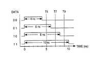
- FIG. 1is a graphic illustration (signal value versus time) of a set of DPPM pulses of various pulse durations for representing a corresponding set of dibit data symbols in accord with the present invention.
- FIGS. 2 a and 2 bare graphical illustrations of DPPM pulse trains in accord with the present invention for a set of exemplary data, showing transmission of a series of 9 high and low going pulses within a single 100 ns system clock period.
- FIG. 3is a schematic circuit diagram of an exemplary DPPM encoder circuit for use in generating DPPM signals that are demodulated by the decoder of the present invention.
- FIG. 4is a schematic circuit diagram of an exemplary DPPM decoder circuit of the present invention.
- the present inventionis a decoder circuit (an embodiment of which is shown in FIG. 4 ) that converts dual phase pulse modulated (DPPM) signals back into their digital data representation.
- DPPMis a method of representing data, resident in digital circuitry in the form of binary circuit states (ones and zeros), as a string of alternating high and low signal pulses whose respective durations or widths represent 2 (or more) bits of data per pulse.
- An exemplary embodiment shown in FIG. 1uses 2 bits for encoding.
- 4, 6, 8, and 10 ns pulse widthsis arbitrary and could just as well have been 4, 5, 6, and 7 ns or some other pulse widths, provided the decoding circuitry at the receiving end of a DPPM signal transmission can correctly distinguish the different pulse widths from each other.
- the data ratecan be considered to be the number of encoded bits per second (or alternatively, the number of pulses per second), which depends on the number of pulses per system clock and on the system clock frequency.
- “Dual Phase”refers to the fact that the information is sent as both the high-going pulses and the low-going pulses. Most pulse width modulation schemes simply vary the width of the high going pulse and therefore are really modulating the duty cycle. DPPM independently modulates the width of both high and low going pulses, with different groups of bits encoded in the high and low portions of each “cycle.” Therefore, clock period and duty cycle are not valid concepts with respect to the generated pulse train. DPPM is by its nature “clockless,” meaning the data can be decoded by simply detecting the width of the pulse with respect to each transition. This means that no clock need be sent with the data, nor must a clock be encoded and recovered from the data.
- FIGS. 2 a and 2 bshow examples of DPPM pulse trains of alternating high and low pulses (5 high pulses and 4 low pulses) transmitting 18 bits of data (organized here as 9 dibits) in a 100 ns system clock period. These 18 bits can form, for example, a 16-bit data word with two error correction code bits appended to the word. Thus one data word may be transmitted per system clock period.
- DPPMSince information is sent on both positive and negative phases of the pulse train, DPPM is by its nature a non-return-to-zero (or non-return-to-one) modulation scheme. However, it is typically desired that the sequence of pulses contained within a system clock period return to zero (or one) at the end of each such sequence. This preference is most easily implemented when, as in the FIGS. 2 a and 2 b examples, the number of multi-bit symbols in a word to be represented as pulses is odd, since the final symbol in the sequence requires a return to zero (or return to one) as the trailing transition of the last pulse. However, this rule needn't be followed if an extra pulse is inserted by the encoder and ignored by the decoder to force a return.
- Mdibits
- Each of the 2 M possible data valuescorresponds to one of 2 M distinct pulse widths, and successive groups of M data bits are represented by signal pulses that are alternately high and low.
- Signal encoding and decoding circuitryperforms the conversion between the data bit and signal pulse representations of the information content.
- received data wordsare first subdivided into an ordered sequence of groups of M data bits, then each group in the sequence is converted into its corresponding signal pulse representation, thus producing a series of high and low signal pulses that represent the data.
- One way to perform the conversion of data words into signal pulsesis to specify signal pulse transition times, each corresponding to a preceding transition time that is incremented by a specified pulse width corresponding to a present group of M data bits, and then producing signal pulse transitions at those specified transition times.
- the exemplary encoder hardwarethat is described below with reference to FIG. 3 performs the conversion in this way.
- the pulse width for each of the high and low signal pulsesis determined, then converted back into an ordered sequence of groups of M data bits, and recombined into data words.
- One way to perform this conversionis carried out by the exemplary decoder hardware set forth in the following description with reference to FIG. 4 .
- an exemplary DPPM encoder circuitreceives data words (e.g., 18 bits grouped into 9 dibits) on a parallel data input bus 11 , here divided into two parts 11 A and 11 B.
- a load signal(not shown) indicates when data is available. If no data is available, the DPPM encoder is held idle.
- Sys_Clock 12is a system clock that is also created externally to the DPPM encoder.
- the circuittakes the received data on the odd and even data buses 11 A and 11 B and, synchronously to the system clock, loads it into two parallel-in, serial-out shift registers 13 A and 13 B.
- the odd bitsi.e., bits 1 , 3 , 5 , 7 , 9 , 11 , 13 , 15 , and 17
- the even bitsi.e., bits 0 , 2 , 4 , 6 , 8 , 10 , 12 , 14 , and 16
- a Shift Clock pulse fed from the multiplexer output 29ensures that successive shifts of data out of the registers 13 A and 13 B are synchronized to the end of each DPPM signal pulse.
- the register outputs 15 A and 15 Bare connected to an input 17 to a state machine 19 , whose N-bit output 21 is a function of its current value and the 2-bit pair to be encoded.
- the state machine 19iteratively increments its state by an amount corresponding to the pulse widths for the successive 2-bit pairs received at state machine input 17 .
- the N-bit output 21has only one active bit and is used as an input 23 to control an multiplexer 25 for selecting the successive taps from the current-controlled delay chain 27 .
- the multiplexer output 29is used to clock a toggle flip-flop 31 and thus encode the data on its output 33 as a series of high and low pulses whose width represents the value of the 2-bit pair.
- An edge detector circuit 14which may be any known edge detector, issues a start pulse of 2 to 3 ns duration at each rising edge of the system clock, Sys_Clock.
- the start pulsealso sets the toggle flip-flop 31 to its ‘set’ state (output high).
- a 1 ns pulse synchronous to the system clockis presented on input 12 to the start of a 92-element delay chain 27 .
- a first delay element 26shown separately, takes into account the time involved in loading the shift registers 13 A and 13 B and presenting the first pair of data bits to the state machine 19 .
- Each element in the delay chain 27is here calibrated to have a 1 ns delay. Therefore, the pulse takes 92 ns to travel down the delay chain. Assuming that a first DPPM signal transition occurs at a time delay of 2 ns (corresponding to tap_select[0]), the delay chain's size corresponds to the maximum total time needed to represent a complete 18-bit word as a series of DPPM signal pulses, when using the set of pulse widths described above for FIG. 1 . That is, a time duration of 90 ns is required to transmit nine “11” bit pairs as nine high and low signal pulses of 10 ns pulse width.
- DLLdelay-locked loop
- the least significant bits in the two shift registers 13 A and 13 Brepresent the current bit pair to be encoded and are input from lines 17 into a tap selector state machine 19 .
- This state machine 19selects a tap point for the 92-element delay chain 27 .
- the pulse widthsmay be 4, 6, 8 or 10 ns for the four possible bit pairs, in which case the valid tap points are only on the even delay elements, so that there are 46 valid tap points in this implementation. (However, the choice of pulse widths is arbitrary and another set of pulse widths could be chosen. The choice of pulse widths is based on the need to provide enough separation such that the decoder can accurately distinguish between them. “Enough” is determined by factors such as desired error/noise margin, amount of noise in the system, and characteristics of the technology used, including process variation, switching speed, and setup/hold requirements.)
- the tap point selection 21is incremented based on the present tap point (STATE(i)) and the next 2-bit data (DATA[1:0]) to be encoded.
- the tap selectsare preferably implemented as a one-shot state machine 19 —essentially a shift register capable of multiple shifts per cycle—where a single active state is incremented by 2, 3, 4, or 5 positions on each clock, depending upon the 2-bit data value input from data lines 17 . While requiring a register for every state is area-inefficient, this implementation allows for extremely fast switching of states and therefore quick control of the multiplexer 25 .
- the tap selection 21that is output from the state machine 19 and the delay chain tap, T 2 through T 92 , that is selected by the multiplexer 25 .
- the timingis such that the tap point must increment to the next value before the rising edge propagating down the delay chain reaches the next tap point.
- the tap point selection 21is the selector control 23 for the multiplexer 25 .
- the output 29 of the multiplexer 25is a 1 ns pulse that occurs once at each selected tap point.
- This multiplexer output 29clocks a toggle flip-flop 31 and also forms the Shift Clock pulse that shifts the data in the shift registers 13 A and 13 B and clocks the state machine 19 from one state to the next.
- the output 33 of the toggle flip-flop 31is the DPPM output of the entire encoder circuit of FIG. 3 .
- an exemplary DPPM decoder circuit of the present inventionprocesses serial DPPM signals received on an input 43 to obtain a parallel data output from an output register 78 .
- Sys_Clockis a system clock that is created externally to the DPPM decoder.
- Deskew blocks 45 and 46allow independent fine-tuning of delay on the DPPM signal that is used for clocking the D-flip-flops 51 A- 51 D and 52 A- 52 D and providing the data that is sampled by those same flip-flops.
- the amount of deskewmay be controlled, for example, by a register (not shown) that tunes a venier circuit in each of the blocks 45 and 46 .
- the high and low pulsesare decoded separately.
- Inverters 48coupled to the DPPM signal input 43 through the deskew blocks 45 and 46 , invert the DPPM signal pulses so that substantially identical subcircuits can be used for decoding both the high and low pulses, as explained further below.
- the value of the datais determined by detecting the pulse widths with respect to the leading edge of each pulse.
- the modulated signal representing the datais piped through a short delay chain and outputs are used to clock and sample the non-delayed signal.
- the decodingrequires no independent or recovered clock.
- the datamay be represented, for example, as 4, 6, 8, and 10 ns pulse widths.
- the length of the pulsecan be determined and then decoded back into its constituent pair of data bits.
- T 5i.e., 5 ns after the pulse leading edge
- a 4 ns pulse encoding the dibit data value 00will already have ended, whereas pulses encoding other dibit data values will not yet have transitioned at their trailing edge to the opposite signal state.
- a 6 ns pulse encoding data value 01will also have ended, and later at time T 9 , an 8 ns pulse encoding data value 10 will have ended, but a 10 ns pulse encoding data value 11 will still continue for another nanosecond.
- the rising edge of a data pulseis sent through a first delay chain 49 and appears at T 5 , T 7 , and T 9 , which are used to clock a set of flip-flops 51 B- 51 D and thus sample the data pulse presented on line 55 .
- the incoming DPPM signalis first inverted, then sent through a second delay chain 50 that is used with another set of flip-flops 52 B- 52 D to sample the inverted data pulse presented on line 56 .
- High and low pulsesare therefore independently decoded.
- the logic AND gates 63 - 66convert the sampled pulse values that are output from the flip-flops 51 - 51 D and 52 B- 52 D on lines 57 B- 57 D and 58 B- 58 D into their corresponding data values.
- the DPPM methodallows for pulse widths to be decoded with respect to the leading edges of pulses, and therefore does not require a clock. This means that no extra clock lines, clock encoding, or clock recovery circuits are required on the receiver. In fact, because delayed versions of the data pulses are actually used to clock (or sample) the incoming non-delayed data pulses, this decoding technique produces an added benefit of eliminating the possibility of introducing error when manipulating or recovering a clock.
Landscapes
- Engineering & Computer Science (AREA)
- Theoretical Computer Science (AREA)
- Dc Digital Transmission (AREA)
- Radar Systems Or Details Thereof (AREA)
- Digital Transmission Methods That Use Modulated Carrier Waves (AREA)
Abstract
Description
00=4 ns pulse
01=6 ns pulse
10=8 ns pulse
11=10 ns pulse
The choice of 4, 6, 8, and 10 ns pulse widths is arbitrary and could just as well have been 4, 5, 6, and 7 ns or some other pulse widths, provided the decoding circuitry at the receiving end of a DPPM signal transmission can correctly distinguish the different pulse widths from each other. The decoding circuitry (as well as process variation, noise and signal degradation, and temperature/voltage variation in the propagating environment) also establishes a practical limit to the number of bits that can be encoded per pulse, with 3 bits per pulse having 8 (=23) possible pulse widths needing to be correctly resolved and 4 bits per pulse having 16 (=24) possible pulse widths needing to be correctly resolved. The data rate can be considered to be the number of encoded bits per second (or alternatively, the number of pulses per second), which depends on the number of pulses per system clock and on the system clock frequency.
Claims (8)
Priority Applications (3)
| Application Number | Priority Date | Filing Date | Title |
|---|---|---|---|
| US10/836,710US6947493B2 (en) | 2003-10-10 | 2004-04-29 | Dual phase pulse modulation decoder circuit |
| PCT/US2004/032744WO2005038479A2 (en) | 2003-10-10 | 2004-10-04 | Dual phase pulse modulation decoder circuit |
| TW093130531ATW200520398A (en) | 2003-10-10 | 2004-10-08 | Dual phase pulse modulation decoder circuit |
Applications Claiming Priority (2)
| Application Number | Priority Date | Filing Date | Title |
|---|---|---|---|
| US50948703P | 2003-10-10 | 2003-10-10 | |
| US10/836,710US6947493B2 (en) | 2003-10-10 | 2004-04-29 | Dual phase pulse modulation decoder circuit |
Publications (2)
| Publication Number | Publication Date |
|---|---|
| US20050078018A1 US20050078018A1 (en) | 2005-04-14 |
| US6947493B2true US6947493B2 (en) | 2005-09-20 |
Family
ID=34426089
Family Applications (1)
| Application Number | Title | Priority Date | Filing Date |
|---|---|---|---|
| US10/836,710Expired - LifetimeUS6947493B2 (en) | 2003-10-10 | 2004-04-29 | Dual phase pulse modulation decoder circuit |
Country Status (3)
| Country | Link |
|---|---|
| US (1) | US6947493B2 (en) |
| TW (1) | TW200520398A (en) |
| WO (1) | WO2005038479A2 (en) |
Cited By (13)
| Publication number | Priority date | Publication date | Assignee | Title |
|---|---|---|---|---|
| US20030210748A1 (en)* | 2002-05-09 | 2003-11-13 | Hiroshi Higashida | Digital signal modulation and demodulation method |
| US20050077976A1 (en)* | 2003-10-10 | 2005-04-14 | Cohen Daniel S. | Method for performing dual phase pulse modulation |
| US20070253478A1 (en)* | 2004-04-16 | 2007-11-01 | Kongsberg Automotive Ab | Method and System for Transmission of Information |
| US20080159379A1 (en)* | 2004-08-23 | 2008-07-03 | Microchip Technology Incorporated | Apparatus for Higher Resolution Pulse Width Modulation Duty Cycle |
| US20080187080A1 (en)* | 2007-02-02 | 2008-08-07 | Tzuen-Hwan Lee | Oversampling data recovery circuit and method for a receiver |
| US20090190756A1 (en)* | 2008-01-29 | 2009-07-30 | Sony Corporation | Systems and Methods for Securing a Digital Communications Link |
| US20100219869A1 (en)* | 2009-02-27 | 2010-09-02 | Fujitsu Microelectronics Limited | Semiconductor intergrated circuit and signal adjusting method |
| US20100260274A1 (en)* | 2009-04-09 | 2010-10-14 | Seiko Epson Corporation | Communication method and communication system |
| US20120213314A1 (en)* | 2011-02-21 | 2012-08-23 | Texas Instruments Incorporated | Digital demodulation of pulse-width modulated signals |
| USH2274H1 (en) | 2009-01-30 | 2013-05-07 | The United States Of America, As Represented By The Secretary Of The Navy | Variable pulse width encoding for information transmission |
| US9100264B2 (en) | 2013-08-22 | 2015-08-04 | M31 Technology Corporation | Digital receiver and method for demodulating pulse-width modulated signals |
| TWI559684B (en)* | 2012-11-20 | 2016-11-21 | 輝達公司 | A matrix phase detector |
| US20220231828A1 (en)* | 2021-01-15 | 2022-07-21 | Realtek Semiconductor Corp. | Receiver and associated signal processing method |
Families Citing this family (11)
| Publication number | Priority date | Publication date | Assignee | Title |
|---|---|---|---|---|
| US7970279B2 (en) | 2002-11-05 | 2011-06-28 | Lightfleet Corporation | N-way serial-channel interconnect |
| JP4290652B2 (en) | 2002-11-05 | 2009-07-08 | ライトフリート コーポレイション | Optical fan-out / broadcast connection |
| US7796885B2 (en) | 2002-11-05 | 2010-09-14 | Lightfleet Corporation | Distribution optical elements and compound collecting lenses for broadcast optical interconnect |
| WO2008097648A1 (en) | 2007-02-07 | 2008-08-14 | Lightfleet Corporation | Fabric generated monotonically increasing identifier |
| WO2008109061A2 (en)* | 2007-03-01 | 2008-09-12 | Lightfleet Corporation | Time domain symbols |
| TW201009586A (en)* | 2008-08-27 | 2010-03-01 | Macroblock Inc | Coordinated operation circuit |
| US9972400B1 (en)* | 2017-08-22 | 2018-05-15 | Inston Inc. | Nonvolatile memory device and calibration method for the same |
| JP2020534723A (en)* | 2017-09-18 | 2020-11-26 | インテル コーポレイション | Time-encoded data communication protocols, devices and methods for generating and receiving data signals |
| US11979177B2 (en) | 2017-09-18 | 2024-05-07 | Intel Corporation | Time encoded data communication protocol, apparatus and method for generating and receiving a data signal |
| US11251996B2 (en)* | 2018-07-24 | 2022-02-15 | Ciphersip Systems Ltd | Modulating signal level transitions to increase data throughput over communication channels |
| IT201900004271A1 (en)* | 2019-03-25 | 2020-09-25 | Massimo Guerci | IMPROVED METHOD FOR CONTEMPORARY TRANSMISSION OF CLOCKS AND DATA ON THE SAME PHYSICAL MEDIA |
Citations (44)
| Publication number | Priority date | Publication date | Assignee | Title |
|---|---|---|---|---|
| US4003085A (en)* | 1974-07-03 | 1977-01-11 | Rca Corporation | Self-clocking, error correcting low bandwidth digital recording system |
| US4049909A (en) | 1975-10-29 | 1977-09-20 | Bell Telephone Laboratories, Incorporated | Digital modulator |
| US4218770A (en) | 1978-09-08 | 1980-08-19 | Bell Telephone Laboratories, Incorporated | Delay modulation data transmission system |
| US4238854A (en)* | 1977-12-05 | 1980-12-09 | International Business Machines Corporation | Cryptographic file security for single domain networks |
| USRE30482E (en) | 1976-06-14 | 1981-01-13 | Lase Industries, Inc. | Pulse code modulated digital audio system |
| US4408166A (en) | 1980-12-29 | 1983-10-04 | Altex Scientific, Inc. | Pulse width modulation decoder |
| US4592072A (en) | 1982-05-07 | 1986-05-27 | Digital Equipment Corp | Decoder for self-clocking serial data communications |
| US4641323A (en) | 1983-02-07 | 1987-02-03 | Tsang Chung K | Multi-phase PSK demodulator |
| US4686484A (en) | 1985-04-17 | 1987-08-11 | Nec Corporation | Phase detection circuit |
| US4931751A (en) | 1989-06-02 | 1990-06-05 | Epyx, Inc. | Apparatus and method for producing pulse width modulated signals from digital information |
| US4951159A (en) | 1989-10-10 | 1990-08-21 | A.I.T. Corporation | Digital modulation technique |
| US5027372A (en) | 1987-03-04 | 1991-06-25 | National Semiconductor Corp. | Differential phase shift keying modulator |
| US5157693A (en) | 1991-04-01 | 1992-10-20 | Motorola, Inc. | Digital modulation circuit |
| US5175549A (en) | 1991-01-17 | 1992-12-29 | Samsung Electronics Co., Ltd. | Pulse width modulation decoder |
| US5202643A (en) | 1991-03-20 | 1993-04-13 | Sony Corporation | Demodulator for demodulating a π/4-shift DQPSK signal |
| US5379323A (en) | 1992-07-02 | 1995-01-03 | Murata Mfg. Co., Ltd. | DQPSK delay detection circuit |
| US5408499A (en) | 1993-01-14 | 1995-04-18 | Nec Corporation | Multilevel code for transmission device |
| US5428321A (en) | 1993-07-30 | 1995-06-27 | Sony Corporation | Pulse width modulator having controlled delay circuit |
| US5442664A (en) | 1993-12-20 | 1995-08-15 | Hewlett-Packard Company | Digitally phase modulated clock inhibiting reduced RF emissions |
| US5506873A (en) | 1992-05-29 | 1996-04-09 | Sony Corporation | Demodulator for a phase shift keying (PSK) signal |
| US5614861A (en) | 1995-05-18 | 1997-03-25 | Mitsubishi Denki Kabushiki Kaisha | N-phase modulated signal demodulation system with carrier reproduction |
| US5625645A (en) | 1995-07-25 | 1997-04-29 | International Business Machines Corporation | Differential pulse encoding and decoding for binary data transmissions |
| US5627500A (en) | 1995-12-26 | 1997-05-06 | Tektronix, Inc. | Phase modulator having individually placed edges |
| US5640160A (en)* | 1994-11-15 | 1997-06-17 | Smk Corporation | Pulse modulation method |
| US5652552A (en) | 1995-03-20 | 1997-07-29 | Hyundai Electronics Industries Co., Ltd. | Phase modulator |
| US5696790A (en)* | 1995-10-04 | 1997-12-09 | Tut Systems, Inc. | Method and apparatus for time dependent data transmission |
| US5841816A (en) | 1992-10-22 | 1998-11-24 | Ericsson Inc. | Diversity Pi/4-DQPSK demodulation |
| US5963074A (en) | 1997-06-18 | 1999-10-05 | Credence Systems Corporation | Programmable delay circuit having calibratable delays |
| US5977821A (en) | 1997-10-20 | 1999-11-02 | Fujitsu Limited | Digital detection method and circuit for PSK modulated signals |
| US6025758A (en) | 1997-10-30 | 2000-02-15 | Uniden San Diego Research & Development Center, Inc. | Method and apparatus for performing digital data signal modulation |
| US6031472A (en)* | 1997-07-23 | 2000-02-29 | And Yet, Inc. | Encoding/detection method for digital data transmitter with a signal having multiple levels |
| US6094450A (en) | 1997-06-20 | 2000-07-25 | Cincinnati Electronics Corporation | Spread spectrum chip shift keying modulation/demodulation system and method |
| US6115428A (en) | 1996-04-04 | 2000-09-05 | Samsung Electronics Co., Ltd. | Apparatus for and method of generating π-/N-shifted N-differential encoded phase shift keying modulation signals |
| US6204726B1 (en) | 1995-11-28 | 2001-03-20 | Sanyo Electric Co., Ltd. | Digital demodulator |
| US6212230B1 (en)* | 1998-04-04 | 2001-04-03 | Sigmatel, Inc. | Method and apparatus for pulse position modulation |
| US6255866B1 (en) | 1998-05-29 | 2001-07-03 | Tektronix, Inc. | Digital phase analyzer and synthesizer |
| US6297691B1 (en) | 2000-06-09 | 2001-10-02 | Rosemount Inc. | Method and apparatus for demodulating coherent and non-coherent modulated signals |
| US6429693B1 (en) | 2000-06-30 | 2002-08-06 | Texas Instruments Incorporated | Digital fractional phase detector |
| US6439679B1 (en) | 2001-06-22 | 2002-08-27 | Hewlett-Packard Company | Pulse with modulation signal generating methods and apparatuses |
| US6473252B1 (en)* | 1998-12-23 | 2002-10-29 | And Yet, Inc. | Biphasic multiple level storage method |
| US20030035496A1 (en) | 2001-08-16 | 2003-02-20 | Nec Corporation | Phase shift keying modulation including a data converter for converting an input data signal having 3 bits long into two ternary converted data signals |
| US20030084079A1 (en)* | 2001-08-08 | 2003-05-01 | Awad Thomas Jefferson | Method and apparatus for providing an error characterization estimate of an impulse response derived using least squares |
| US20030198478A1 (en) | 2002-04-23 | 2003-10-23 | Quellan, Inc. | Method and system for generating and decoding a bandwidth efficient multi-level signal |
| US20040095264A1 (en)* | 2002-11-14 | 2004-05-20 | Thomas John Carl | Power converter circuitry and method |
- 2004
- 2004-04-29USUS10/836,710patent/US6947493B2/ennot_activeExpired - Lifetime
- 2004-10-04WOPCT/US2004/032744patent/WO2005038479A2/enactiveApplication Filing
- 2004-10-08TWTW093130531Apatent/TW200520398A/enunknown
Patent Citations (45)
| Publication number | Priority date | Publication date | Assignee | Title |
|---|---|---|---|---|
| US4003085A (en)* | 1974-07-03 | 1977-01-11 | Rca Corporation | Self-clocking, error correcting low bandwidth digital recording system |
| US4049909A (en) | 1975-10-29 | 1977-09-20 | Bell Telephone Laboratories, Incorporated | Digital modulator |
| USRE30482E (en) | 1976-06-14 | 1981-01-13 | Lase Industries, Inc. | Pulse code modulated digital audio system |
| US4238854A (en)* | 1977-12-05 | 1980-12-09 | International Business Machines Corporation | Cryptographic file security for single domain networks |
| US4218770A (en) | 1978-09-08 | 1980-08-19 | Bell Telephone Laboratories, Incorporated | Delay modulation data transmission system |
| US4408166A (en) | 1980-12-29 | 1983-10-04 | Altex Scientific, Inc. | Pulse width modulation decoder |
| US4592072A (en) | 1982-05-07 | 1986-05-27 | Digital Equipment Corp | Decoder for self-clocking serial data communications |
| US4592072B1 (en) | 1982-05-07 | 1994-02-15 | Digital Equipment Corporation | Decoder for self-clocking serial data communications |
| US4641323A (en) | 1983-02-07 | 1987-02-03 | Tsang Chung K | Multi-phase PSK demodulator |
| US4686484A (en) | 1985-04-17 | 1987-08-11 | Nec Corporation | Phase detection circuit |
| US5027372A (en) | 1987-03-04 | 1991-06-25 | National Semiconductor Corp. | Differential phase shift keying modulator |
| US4931751A (en) | 1989-06-02 | 1990-06-05 | Epyx, Inc. | Apparatus and method for producing pulse width modulated signals from digital information |
| US4951159A (en) | 1989-10-10 | 1990-08-21 | A.I.T. Corporation | Digital modulation technique |
| US5175549A (en) | 1991-01-17 | 1992-12-29 | Samsung Electronics Co., Ltd. | Pulse width modulation decoder |
| US5202643A (en) | 1991-03-20 | 1993-04-13 | Sony Corporation | Demodulator for demodulating a π/4-shift DQPSK signal |
| US5157693A (en) | 1991-04-01 | 1992-10-20 | Motorola, Inc. | Digital modulation circuit |
| US5506873A (en) | 1992-05-29 | 1996-04-09 | Sony Corporation | Demodulator for a phase shift keying (PSK) signal |
| US5379323A (en) | 1992-07-02 | 1995-01-03 | Murata Mfg. Co., Ltd. | DQPSK delay detection circuit |
| US5841816A (en) | 1992-10-22 | 1998-11-24 | Ericsson Inc. | Diversity Pi/4-DQPSK demodulation |
| US5408499A (en) | 1993-01-14 | 1995-04-18 | Nec Corporation | Multilevel code for transmission device |
| US5428321A (en) | 1993-07-30 | 1995-06-27 | Sony Corporation | Pulse width modulator having controlled delay circuit |
| US5442664A (en) | 1993-12-20 | 1995-08-15 | Hewlett-Packard Company | Digitally phase modulated clock inhibiting reduced RF emissions |
| US5640160A (en)* | 1994-11-15 | 1997-06-17 | Smk Corporation | Pulse modulation method |
| US5652552A (en) | 1995-03-20 | 1997-07-29 | Hyundai Electronics Industries Co., Ltd. | Phase modulator |
| US5614861A (en) | 1995-05-18 | 1997-03-25 | Mitsubishi Denki Kabushiki Kaisha | N-phase modulated signal demodulation system with carrier reproduction |
| US5625645A (en) | 1995-07-25 | 1997-04-29 | International Business Machines Corporation | Differential pulse encoding and decoding for binary data transmissions |
| US5696790A (en)* | 1995-10-04 | 1997-12-09 | Tut Systems, Inc. | Method and apparatus for time dependent data transmission |
| US6204726B1 (en) | 1995-11-28 | 2001-03-20 | Sanyo Electric Co., Ltd. | Digital demodulator |
| US5627500A (en) | 1995-12-26 | 1997-05-06 | Tektronix, Inc. | Phase modulator having individually placed edges |
| US6115428A (en) | 1996-04-04 | 2000-09-05 | Samsung Electronics Co., Ltd. | Apparatus for and method of generating π-/N-shifted N-differential encoded phase shift keying modulation signals |
| US5963074A (en) | 1997-06-18 | 1999-10-05 | Credence Systems Corporation | Programmable delay circuit having calibratable delays |
| US6094450A (en) | 1997-06-20 | 2000-07-25 | Cincinnati Electronics Corporation | Spread spectrum chip shift keying modulation/demodulation system and method |
| US6031472A (en)* | 1997-07-23 | 2000-02-29 | And Yet, Inc. | Encoding/detection method for digital data transmitter with a signal having multiple levels |
| US5977821A (en) | 1997-10-20 | 1999-11-02 | Fujitsu Limited | Digital detection method and circuit for PSK modulated signals |
| US6025758A (en) | 1997-10-30 | 2000-02-15 | Uniden San Diego Research & Development Center, Inc. | Method and apparatus for performing digital data signal modulation |
| US6212230B1 (en)* | 1998-04-04 | 2001-04-03 | Sigmatel, Inc. | Method and apparatus for pulse position modulation |
| US6255866B1 (en) | 1998-05-29 | 2001-07-03 | Tektronix, Inc. | Digital phase analyzer and synthesizer |
| US6473252B1 (en)* | 1998-12-23 | 2002-10-29 | And Yet, Inc. | Biphasic multiple level storage method |
| US6297691B1 (en) | 2000-06-09 | 2001-10-02 | Rosemount Inc. | Method and apparatus for demodulating coherent and non-coherent modulated signals |
| US6429693B1 (en) | 2000-06-30 | 2002-08-06 | Texas Instruments Incorporated | Digital fractional phase detector |
| US6439679B1 (en) | 2001-06-22 | 2002-08-27 | Hewlett-Packard Company | Pulse with modulation signal generating methods and apparatuses |
| US20030084079A1 (en)* | 2001-08-08 | 2003-05-01 | Awad Thomas Jefferson | Method and apparatus for providing an error characterization estimate of an impulse response derived using least squares |
| US20030035496A1 (en) | 2001-08-16 | 2003-02-20 | Nec Corporation | Phase shift keying modulation including a data converter for converting an input data signal having 3 bits long into two ternary converted data signals |
| US20030198478A1 (en) | 2002-04-23 | 2003-10-23 | Quellan, Inc. | Method and system for generating and decoding a bandwidth efficient multi-level signal |
| US20040095264A1 (en)* | 2002-11-14 | 2004-05-20 | Thomas John Carl | Power converter circuitry and method |
Cited By (30)
| Publication number | Priority date | Publication date | Assignee | Title |
|---|---|---|---|---|
| US20030210748A1 (en)* | 2002-05-09 | 2003-11-13 | Hiroshi Higashida | Digital signal modulation and demodulation method |
| US20050077976A1 (en)* | 2003-10-10 | 2005-04-14 | Cohen Daniel S. | Method for performing dual phase pulse modulation |
| US7283011B2 (en)* | 2003-10-10 | 2007-10-16 | Atmel Corporation | Method for performing dual phase pulse modulation |
| US20070253478A1 (en)* | 2004-04-16 | 2007-11-01 | Kongsberg Automotive Ab | Method and System for Transmission of Information |
| US20080159381A1 (en)* | 2004-08-23 | 2008-07-03 | Microchip Technology Incorporated | Apparatus and Method for Generating Push-Pull Pulse Width Modulation Signals |
| US20080159382A1 (en)* | 2004-08-23 | 2008-07-03 | Bryan Kris | Apparatus and Method for Generating Current Reset Mode Pulse Width Modulation Signals |
| US7593500B2 (en)* | 2004-08-23 | 2009-09-22 | Microchip Technology Incorporated | Apparatus for coordinating triggering of analog-to-digital conversions relative to pulse width modulation cycle timing |
| US20080159379A1 (en)* | 2004-08-23 | 2008-07-03 | Microchip Technology Incorporated | Apparatus for Higher Resolution Pulse Width Modulation Duty Cycle |
| US7433404B2 (en)* | 2004-08-23 | 2008-10-07 | Microchip Technology Incorporated | Apparatus for higher resolution pulse width modulation duty cycle |
| US7502436B2 (en)* | 2004-08-23 | 2009-03-10 | Microchip Technology Incorporated | Apparatus and method for generating push-pull pulse width modulation signals |
| US7508900B2 (en)* | 2004-08-23 | 2009-03-24 | Microchip Technology Incorporated | Apparatus for improved resolution pulse width modulation module duty cycle, dead time and phase |
| US7508901B2 (en)* | 2004-08-23 | 2009-03-24 | Microchip Technology Incorporated | Apparatus and method for generating current reset mode pulse width modulation signals |
| US7508899B2 (en)* | 2004-08-23 | 2009-03-24 | Microchip Technology Incorporated | Apparatus and method for generating multi-phase pulse width modulation (PWM) and sharing a common (master) duty cycle value among a plurality of PWM generators |
| US20080187080A1 (en)* | 2007-02-02 | 2008-08-07 | Tzuen-Hwan Lee | Oversampling data recovery circuit and method for a receiver |
| US7936855B2 (en)* | 2007-02-02 | 2011-05-03 | Ite Tech. Inc. | Oversampling data recovery circuit and method for a receiver |
| US20090190756A1 (en)* | 2008-01-29 | 2009-07-30 | Sony Corporation | Systems and Methods for Securing a Digital Communications Link |
| US9338412B2 (en) | 2008-01-29 | 2016-05-10 | Sony Corporation | Systems and methods for securing a digital communications link |
| US8792640B2 (en)* | 2008-01-29 | 2014-07-29 | Sony Corporation | Systems and methods for securing a digital communications link |
| USH2274H1 (en) | 2009-01-30 | 2013-05-07 | The United States Of America, As Represented By The Secretary Of The Navy | Variable pulse width encoding for information transmission |
| US8891355B1 (en) | 2009-01-30 | 2014-11-18 | The United States Of America As Represented By The Secretary Of The Navy | Information transmitter with variable pulse width encoding |
| US8049547B2 (en)* | 2009-02-27 | 2011-11-01 | Fujitsu Semiconductor Limited | Semiconductor integrated circuit and signal adjusting method |
| US20100219869A1 (en)* | 2009-02-27 | 2010-09-02 | Fujitsu Microelectronics Limited | Semiconductor intergrated circuit and signal adjusting method |
| US8363751B2 (en)* | 2009-04-09 | 2013-01-29 | Seiko Epson Corporation | Communication method and communication system |
| US20100260274A1 (en)* | 2009-04-09 | 2010-10-14 | Seiko Epson Corporation | Communication method and communication system |
| US20120213314A1 (en)* | 2011-02-21 | 2012-08-23 | Texas Instruments Incorporated | Digital demodulation of pulse-width modulated signals |
| US8411804B2 (en)* | 2011-02-21 | 2013-04-02 | Texas Instruments Incorporated | Digital demodulation of pulse-width modulated signals |
| TWI559684B (en)* | 2012-11-20 | 2016-11-21 | 輝達公司 | A matrix phase detector |
| US9100264B2 (en) | 2013-08-22 | 2015-08-04 | M31 Technology Corporation | Digital receiver and method for demodulating pulse-width modulated signals |
| US20220231828A1 (en)* | 2021-01-15 | 2022-07-21 | Realtek Semiconductor Corp. | Receiver and associated signal processing method |
| US11671236B2 (en)* | 2021-01-15 | 2023-06-06 | Realtek Semiconductor Corp. | Receiver and associated signal processing method |
Also Published As
| Publication number | Publication date |
|---|---|
| US20050078018A1 (en) | 2005-04-14 |
| TW200520398A (en) | 2005-06-16 |
| WO2005038479A3 (en) | 2005-12-01 |
| WO2005038479A2 (en) | 2005-04-28 |
Similar Documents
| Publication | Publication Date | Title |
|---|---|---|
| US6947493B2 (en) | Dual phase pulse modulation decoder circuit | |
| US7103110B2 (en) | Dual phase pulse modulation encoder circuit | |
| JP5066121B2 (en) | Apparatus and method for transmitting clock information and data | |
| US20060198463A1 (en) | Device for converting a transmitted signal into a digital signal | |
| KR100868299B1 (en) | Method and apparatus for transmitting data with clock information | |
| US7283011B2 (en) | Method for performing dual phase pulse modulation | |
| WO2007037312A1 (en) | Clock reproduction device and method | |
| US8144761B2 (en) | Pulse transmission method, pulse transmission system, transmitter, and receiver | |
| US7079577B2 (en) | Wide window decoder circuit for dual phase pulse modulation | |
| CN100589464C (en) | Bi-phase pulse modulation encoder circuit | |
| US7260151B2 (en) | Dual phase pulse modulation system | |
| JP2005210695A (en) | Data transmission method and data transmission circuit | |
| KR100899781B1 (en) | Method and apparatus for transmitting data with clock information | |
| KR101272886B1 (en) | apparatus and method for transmitting data with clock information | |
| CN1883117A (en) | Method for performing dual phase pulse modulation | |
| JP5369524B2 (en) | Clock data recovery circuit | |
| CN100581202C (en) | Bi-phase pulse modulation decoder circuit | |
| US20070069927A1 (en) | Method of transmitting a serial bit-stream and electronic transmitter for transmitting a serial bit-stream | |
| JP5116567B2 (en) | Optical receiver | |
| US7057538B1 (en) | 1/N-rate encoder circuit topology | |
| EP2252024B1 (en) | Swap tolerant coding and decoding circuits and methods | |
| JP2621717B2 (en) | Receive burst synchronization circuit | |
| JP3458782B2 (en) | DUTY correction circuit | |
| JP2005159523A (en) | PPM demodulation circuit and PPM demodulation method | |
| EP2913928A1 (en) | Circuitry and method for converting a multi-level signal into at least one binary signal |
Legal Events
| Date | Code | Title | Description |
|---|---|---|---|
| AS | Assignment | Owner name:ATMEL CORPORATION, CALIFORNIA Free format text:ASSIGNMENT OF ASSIGNORS INTEREST;ASSIGNORS:COHEN, DANIEL S.;MEYER, DANIEL J.;REEL/FRAME:015327/0316 Effective date:20040427 | |
| STCF | Information on status: patent grant | Free format text:PATENTED CASE | |
| CC | Certificate of correction | ||
| FEPP | Fee payment procedure | Free format text:PAYOR NUMBER ASSIGNED (ORIGINAL EVENT CODE: ASPN); ENTITY STATUS OF PATENT OWNER: LARGE ENTITY | |
| FPAY | Fee payment | Year of fee payment:4 | |
| FPAY | Fee payment | Year of fee payment:8 | |
| AS | Assignment | Owner name:MORGAN STANLEY SENIOR FUNDING, INC. AS ADMINISTRATIVE AGENT, NEW YORK Free format text:PATENT SECURITY AGREEMENT;ASSIGNOR:ATMEL CORPORATION;REEL/FRAME:031912/0173 Effective date:20131206 Owner name:MORGAN STANLEY SENIOR FUNDING, INC. AS ADMINISTRAT Free format text:PATENT SECURITY AGREEMENT;ASSIGNOR:ATMEL CORPORATION;REEL/FRAME:031912/0173 Effective date:20131206 | |
| AS | Assignment | Owner name:ATMEL CORPORATION, CALIFORNIA Free format text:TERMINATION AND RELEASE OF SECURITY INTEREST IN PATENT COLLATERAL;ASSIGNOR:MORGAN STANLEY SENIOR FUNDING, INC.;REEL/FRAME:038376/0001 Effective date:20160404 | |
| AS | Assignment | Owner name:JPMORGAN CHASE BANK, N.A., AS ADMINISTRATIVE AGENT, ILLINOIS Free format text:SECURITY INTEREST;ASSIGNOR:ATMEL CORPORATION;REEL/FRAME:041715/0747 Effective date:20170208 Owner name:JPMORGAN CHASE BANK, N.A., AS ADMINISTRATIVE AGENT Free format text:SECURITY INTEREST;ASSIGNOR:ATMEL CORPORATION;REEL/FRAME:041715/0747 Effective date:20170208 | |
| FPAY | Fee payment | Year of fee payment:12 | |
| AS | Assignment | Owner name:JPMORGAN CHASE BANK, N.A., AS ADMINISTRATIVE AGENT, ILLINOIS Free format text:SECURITY INTEREST;ASSIGNORS:MICROCHIP TECHNOLOGY INCORPORATED;SILICON STORAGE TECHNOLOGY, INC.;ATMEL CORPORATION;AND OTHERS;REEL/FRAME:046426/0001 Effective date:20180529 Owner name:JPMORGAN CHASE BANK, N.A., AS ADMINISTRATIVE AGENT Free format text:SECURITY INTEREST;ASSIGNORS:MICROCHIP TECHNOLOGY INCORPORATED;SILICON STORAGE TECHNOLOGY, INC.;ATMEL CORPORATION;AND OTHERS;REEL/FRAME:046426/0001 Effective date:20180529 | |
| AS | Assignment | Owner name:WELLS FARGO BANK, NATIONAL ASSOCIATION, AS NOTES COLLATERAL AGENT, CALIFORNIA Free format text:SECURITY INTEREST;ASSIGNORS:MICROCHIP TECHNOLOGY INCORPORATED;SILICON STORAGE TECHNOLOGY, INC.;ATMEL CORPORATION;AND OTHERS;REEL/FRAME:047103/0206 Effective date:20180914 Owner name:WELLS FARGO BANK, NATIONAL ASSOCIATION, AS NOTES C Free format text:SECURITY INTEREST;ASSIGNORS:MICROCHIP TECHNOLOGY INCORPORATED;SILICON STORAGE TECHNOLOGY, INC.;ATMEL CORPORATION;AND OTHERS;REEL/FRAME:047103/0206 Effective date:20180914 | |
| AS | Assignment | Owner name:JPMORGAN CHASE BANK, N.A., AS ADMINISTRATIVE AGENT, DELAWARE Free format text:SECURITY INTEREST;ASSIGNORS:MICROCHIP TECHNOLOGY INC.;SILICON STORAGE TECHNOLOGY, INC.;ATMEL CORPORATION;AND OTHERS;REEL/FRAME:053311/0305 Effective date:20200327 | |
| AS | Assignment | Owner name:ATMEL CORPORATION, ARIZONA Free format text:RELEASE BY SECURED PARTY;ASSIGNOR:JPMORGAN CHASE BANK, N.A, AS ADMINISTRATIVE AGENT;REEL/FRAME:053466/0011 Effective date:20200529 Owner name:MICROSEMI CORPORATION, CALIFORNIA Free format text:RELEASE BY SECURED PARTY;ASSIGNOR:JPMORGAN CHASE BANK, N.A, AS ADMINISTRATIVE AGENT;REEL/FRAME:053466/0011 Effective date:20200529 Owner name:SILICON STORAGE TECHNOLOGY, INC., ARIZONA Free format text:RELEASE BY SECURED PARTY;ASSIGNOR:JPMORGAN CHASE BANK, N.A, AS ADMINISTRATIVE AGENT;REEL/FRAME:053466/0011 Effective date:20200529 Owner name:MICROSEMI STORAGE SOLUTIONS, INC., ARIZONA Free format text:RELEASE BY SECURED PARTY;ASSIGNOR:JPMORGAN CHASE BANK, N.A, AS ADMINISTRATIVE AGENT;REEL/FRAME:053466/0011 Effective date:20200529 Owner name:MICROCHIP TECHNOLOGY INC., ARIZONA Free format text:RELEASE BY SECURED PARTY;ASSIGNOR:JPMORGAN CHASE BANK, N.A, AS ADMINISTRATIVE AGENT;REEL/FRAME:053466/0011 Effective date:20200529 | |
| AS | Assignment | Owner name:WELLS FARGO BANK, NATIONAL ASSOCIATION, MINNESOTA Free format text:SECURITY INTEREST;ASSIGNORS:MICROCHIP TECHNOLOGY INC.;SILICON STORAGE TECHNOLOGY, INC.;ATMEL CORPORATION;AND OTHERS;REEL/FRAME:053468/0705 Effective date:20200529 | |
| AS | Assignment | Owner name:WELLS FARGO BANK, NATIONAL ASSOCIATION, AS COLLATERAL AGENT, MINNESOTA Free format text:SECURITY INTEREST;ASSIGNORS:MICROCHIP TECHNOLOGY INCORPORATED;SILICON STORAGE TECHNOLOGY, INC.;ATMEL CORPORATION;AND OTHERS;REEL/FRAME:055671/0612 Effective date:20201217 | |
| AS | Assignment | Owner name:WELLS FARGO BANK, NATIONAL ASSOCIATION, AS NOTES COLLATERAL AGENT, MINNESOTA Free format text:SECURITY INTEREST;ASSIGNORS:MICROCHIP TECHNOLOGY INCORPORATED;SILICON STORAGE TECHNOLOGY, INC.;ATMEL CORPORATION;AND OTHERS;REEL/FRAME:057935/0474 Effective date:20210528 | |
| AS | Assignment | Owner name:MICROSEMI STORAGE SOLUTIONS, INC., ARIZONA Free format text:RELEASE BY SECURED PARTY;ASSIGNOR:JPMORGAN CHASE BANK, N.A., AS ADMINISTRATIVE AGENT;REEL/FRAME:059333/0222 Effective date:20220218 Owner name:MICROSEMI CORPORATION, ARIZONA Free format text:RELEASE BY SECURED PARTY;ASSIGNOR:JPMORGAN CHASE BANK, N.A., AS ADMINISTRATIVE AGENT;REEL/FRAME:059333/0222 Effective date:20220218 Owner name:ATMEL CORPORATION, ARIZONA Free format text:RELEASE BY SECURED PARTY;ASSIGNOR:JPMORGAN CHASE BANK, N.A., AS ADMINISTRATIVE AGENT;REEL/FRAME:059333/0222 Effective date:20220218 Owner name:SILICON STORAGE TECHNOLOGY, INC., ARIZONA Free format text:RELEASE BY SECURED PARTY;ASSIGNOR:JPMORGAN CHASE BANK, N.A., AS ADMINISTRATIVE AGENT;REEL/FRAME:059333/0222 Effective date:20220218 Owner name:MICROCHIP TECHNOLOGY INCORPORATED, ARIZONA Free format text:RELEASE BY SECURED PARTY;ASSIGNOR:JPMORGAN CHASE BANK, N.A., AS ADMINISTRATIVE AGENT;REEL/FRAME:059333/0222 Effective date:20220218 | |
| AS | Assignment | Owner name:ATMEL CORPORATION, ARIZONA Free format text:RELEASE BY SECURED PARTY;ASSIGNOR:JPMORGAN CHASE BANK, N.A., AS ADMINISTRATIVE AGENT;REEL/FRAME:059262/0105 Effective date:20220218 | |
| AS | Assignment | Owner name:MICROSEMI STORAGE SOLUTIONS, INC., ARIZONA Free format text:RELEASE BY SECURED PARTY;ASSIGNOR:WELLS FARGO BANK, NATIONAL ASSOCIATION, AS NOTES COLLATERAL AGENT;REEL/FRAME:059358/0001 Effective date:20220228 Owner name:MICROSEMI CORPORATION, ARIZONA Free format text:RELEASE BY SECURED PARTY;ASSIGNOR:WELLS FARGO BANK, NATIONAL ASSOCIATION, AS NOTES COLLATERAL AGENT;REEL/FRAME:059358/0001 Effective date:20220228 Owner name:ATMEL CORPORATION, ARIZONA Free format text:RELEASE BY SECURED PARTY;ASSIGNOR:WELLS FARGO BANK, NATIONAL ASSOCIATION, AS NOTES COLLATERAL AGENT;REEL/FRAME:059358/0001 Effective date:20220228 Owner name:SILICON STORAGE TECHNOLOGY, INC., ARIZONA Free format text:RELEASE BY SECURED PARTY;ASSIGNOR:WELLS FARGO BANK, NATIONAL ASSOCIATION, AS NOTES COLLATERAL AGENT;REEL/FRAME:059358/0001 Effective date:20220228 Owner name:MICROCHIP TECHNOLOGY INCORPORATED, ARIZONA Free format text:RELEASE BY SECURED PARTY;ASSIGNOR:WELLS FARGO BANK, NATIONAL ASSOCIATION, AS NOTES COLLATERAL AGENT;REEL/FRAME:059358/0001 Effective date:20220228 | |
| AS | Assignment | Owner name:MICROSEMI STORAGE SOLUTIONS, INC., ARIZONA Free format text:RELEASE BY SECURED PARTY;ASSIGNOR:WELLS FARGO BANK, NATIONAL ASSOCIATION, AS NOTES COLLATERAL AGENT;REEL/FRAME:059863/0400 Effective date:20220228 Owner name:MICROSEMI CORPORATION, ARIZONA Free format text:RELEASE BY SECURED PARTY;ASSIGNOR:WELLS FARGO BANK, NATIONAL ASSOCIATION, AS NOTES COLLATERAL AGENT;REEL/FRAME:059863/0400 Effective date:20220228 Owner name:ATMEL CORPORATION, ARIZONA Free format text:RELEASE BY SECURED PARTY;ASSIGNOR:WELLS FARGO BANK, NATIONAL ASSOCIATION, AS NOTES COLLATERAL AGENT;REEL/FRAME:059863/0400 Effective date:20220228 Owner name:SILICON STORAGE TECHNOLOGY, INC., ARIZONA Free format text:RELEASE BY SECURED PARTY;ASSIGNOR:WELLS FARGO BANK, NATIONAL ASSOCIATION, AS NOTES COLLATERAL AGENT;REEL/FRAME:059863/0400 Effective date:20220228 Owner name:MICROCHIP TECHNOLOGY INCORPORATED, ARIZONA Free format text:RELEASE BY SECURED PARTY;ASSIGNOR:WELLS FARGO BANK, NATIONAL ASSOCIATION, AS NOTES COLLATERAL AGENT;REEL/FRAME:059863/0400 Effective date:20220228 | |
| AS | Assignment | Owner name:MICROSEMI STORAGE SOLUTIONS, INC., ARIZONA Free format text:RELEASE BY SECURED PARTY;ASSIGNOR:WELLS FARGO BANK, NATIONAL ASSOCIATION, AS NOTES COLLATERAL AGENT;REEL/FRAME:059363/0001 Effective date:20220228 Owner name:MICROSEMI CORPORATION, ARIZONA Free format text:RELEASE BY SECURED PARTY;ASSIGNOR:WELLS FARGO BANK, NATIONAL ASSOCIATION, AS NOTES COLLATERAL AGENT;REEL/FRAME:059363/0001 Effective date:20220228 Owner name:ATMEL CORPORATION, ARIZONA Free format text:RELEASE BY SECURED PARTY;ASSIGNOR:WELLS FARGO BANK, NATIONAL ASSOCIATION, AS NOTES COLLATERAL AGENT;REEL/FRAME:059363/0001 Effective date:20220228 Owner name:SILICON STORAGE TECHNOLOGY, INC., ARIZONA Free format text:RELEASE BY SECURED PARTY;ASSIGNOR:WELLS FARGO BANK, NATIONAL ASSOCIATION, AS NOTES COLLATERAL AGENT;REEL/FRAME:059363/0001 Effective date:20220228 Owner name:MICROCHIP TECHNOLOGY INCORPORATED, ARIZONA Free format text:RELEASE BY SECURED PARTY;ASSIGNOR:WELLS FARGO BANK, NATIONAL ASSOCIATION, AS NOTES COLLATERAL AGENT;REEL/FRAME:059363/0001 Effective date:20220228 | |
| AS | Assignment | Owner name:MICROSEMI STORAGE SOLUTIONS, INC., ARIZONA Free format text:RELEASE BY SECURED PARTY;ASSIGNOR:WELLS FARGO BANK, NATIONAL ASSOCIATION, AS NOTES COLLATERAL AGENT;REEL/FRAME:060894/0437 Effective date:20220228 Owner name:MICROSEMI CORPORATION, ARIZONA Free format text:RELEASE BY SECURED PARTY;ASSIGNOR:WELLS FARGO BANK, NATIONAL ASSOCIATION, AS NOTES COLLATERAL AGENT;REEL/FRAME:060894/0437 Effective date:20220228 Owner name:ATMEL CORPORATION, ARIZONA Free format text:RELEASE BY SECURED PARTY;ASSIGNOR:WELLS FARGO BANK, NATIONAL ASSOCIATION, AS NOTES COLLATERAL AGENT;REEL/FRAME:060894/0437 Effective date:20220228 Owner name:SILICON STORAGE TECHNOLOGY, INC., ARIZONA Free format text:RELEASE BY SECURED PARTY;ASSIGNOR:WELLS FARGO BANK, NATIONAL ASSOCIATION, AS NOTES COLLATERAL AGENT;REEL/FRAME:060894/0437 Effective date:20220228 Owner name:MICROCHIP TECHNOLOGY INCORPORATED, ARIZONA Free format text:RELEASE BY SECURED PARTY;ASSIGNOR:WELLS FARGO BANK, NATIONAL ASSOCIATION, AS NOTES COLLATERAL AGENT;REEL/FRAME:060894/0437 Effective date:20220228 |