US6947235B2 - Patterned multilevel perpendicular magnetic recording media - Google Patents
Patterned multilevel perpendicular magnetic recording mediaDownload PDFInfo
- Publication number
- US6947235B2 US6947235B2US10/727,826US72782603AUS6947235B2US 6947235 B2US6947235 B2US 6947235B2US 72782603 AUS72782603 AUS 72782603AUS 6947235 B2US6947235 B2US 6947235B2
- Authority
- US
- United States
- Prior art keywords
- magnetic
- medium
- substrate
- islands
- island
- Prior art date
- Legal status (The legal status is an assumption and is not a legal conclusion. Google has not performed a legal analysis and makes no representation as to the accuracy of the status listed.)
- Expired - Lifetime
Links
- 230000005291magnetic effectEffects0.000titleclaimsabstractdescription189
- 239000000463materialSubstances0.000claimsabstractdescription31
- 125000006850spacer groupChemical group0.000claimsabstractdescription10
- 230000005381magnetic domainEffects0.000claimsabstractdescription8
- 239000000758substrateSubstances0.000claimsdescription38
- VYPSYNLAJGMNEJ-UHFFFAOYSA-NSilicium dioxideChemical compoundO=[Si]=OVYPSYNLAJGMNEJ-UHFFFAOYSA-N0.000claimsdescription16
- 239000000956alloySubstances0.000claimsdescription8
- 229910052681coesiteInorganic materials0.000claimsdescription8
- 229910052906cristobaliteInorganic materials0.000claimsdescription8
- 239000000377silicon dioxideSubstances0.000claimsdescription8
- 229910052682stishoviteInorganic materials0.000claimsdescription8
- 229910052905tridymiteInorganic materials0.000claimsdescription8
- 229910045601alloyInorganic materials0.000claimsdescription7
- 239000010952cobalt-chromeSubstances0.000claimsdescription7
- 229910000684Cobalt-chromeInorganic materials0.000claimsdescription6
- 239000003302ferromagnetic materialSubstances0.000claimsdescription6
- 229910019236CoFeBInorganic materials0.000claimsdescription3
- -1FeAlSiInorganic materials0.000claimsdescription3
- 229910015140FeNInorganic materials0.000claimsdescription3
- 229910005435FeTaNInorganic materials0.000claimsdescription3
- 229910001030Iron–nickel alloyInorganic materials0.000claimsdescription3
- 229910000943NiAlInorganic materials0.000claimsdescription3
- NPXOKRUENSOPAO-UHFFFAOYSA-NRaney nickelChemical compound[Al].[Ni]NPXOKRUENSOPAO-UHFFFAOYSA-N0.000claimsdescription3
- 229910010169TiCrInorganic materials0.000claimsdescription3
- 229910052763palladiumInorganic materials0.000claimsdescription3
- 229910052697platinumInorganic materials0.000claimsdescription3
- 230000002708enhancing effectEffects0.000claims4
- 229910052742ironInorganic materials0.000claims4
- 229910052804chromiumInorganic materials0.000claims2
- 229910052759nickelInorganic materials0.000claims2
- 230000005415magnetizationEffects0.000abstractdescription35
- 239000000523sampleSubstances0.000description38
- 230000001939inductive effectEffects0.000description22
- 238000002465magnetic force microscopyMethods0.000description15
- 238000000034methodMethods0.000description13
- 239000000696magnetic materialSubstances0.000description7
- 150000002500ionsChemical class0.000description6
- 230000005374Kerr effectEffects0.000description4
- PNEYBMLMFCGWSK-UHFFFAOYSA-Naluminium oxideInorganic materials[O-2].[O-2].[O-2].[Al+3].[Al+3]PNEYBMLMFCGWSK-UHFFFAOYSA-N0.000description4
- 239000010408filmSubstances0.000description4
- 238000004519manufacturing processMethods0.000description4
- 238000000059patterningMethods0.000description4
- 230000008878couplingEffects0.000description3
- 238000010168coupling processMethods0.000description3
- 238000005859coupling reactionMethods0.000description3
- 238000000151depositionMethods0.000description3
- 230000008569processEffects0.000description3
- 238000003860storageMethods0.000description3
- 239000000725suspensionSubstances0.000description3
- 239000010409thin filmSubstances0.000description3
- 229910018936CoPdInorganic materials0.000description2
- 229910018979CoPtInorganic materials0.000description2
- 229910015187FePdInorganic materials0.000description2
- 229910005335FePtInorganic materials0.000description2
- 230000002411adverseEffects0.000description2
- SNAAJJQQZSMGQD-UHFFFAOYSA-Naluminum magnesiumChemical compound[Mg].[Al]SNAAJJQQZSMGQD-UHFFFAOYSA-N0.000description2
- 230000008901benefitEffects0.000description2
- 238000013500data storageMethods0.000description2
- 238000002474experimental methodMethods0.000description2
- 230000004907fluxEffects0.000description2
- 239000011521glassSubstances0.000description2
- 238000010438heat treatmentMethods0.000description2
- 241000258963DiplopodaSpecies0.000description1
- 230000008859changeEffects0.000description1
- 239000011651chromiumSubstances0.000description1
- 229910052802copperInorganic materials0.000description1
- RKTYLMNFRDHKIL-UHFFFAOYSA-Ncopper;5,10,15,20-tetraphenylporphyrin-22,24-diideChemical compound[Cu+2].C1=CC(C(=C2C=CC([N-]2)=C(C=2C=CC=CC=2)C=2C=CC(N=2)=C(C=2C=CC=CC=2)C2=CC=C3[N-]2)C=2C=CC=CC=2)=NC1=C3C1=CC=CC=C1RKTYLMNFRDHKIL-UHFFFAOYSA-N0.000description1
- 230000007547defectEffects0.000description1
- 238000001514detection methodMethods0.000description1
- 238000005530etchingMethods0.000description1
- 229910052737goldInorganic materials0.000description1
- 230000003993interactionEffects0.000description1
- 238000005259measurementMethods0.000description1
- 239000000203mixtureSubstances0.000description1
- 239000002086nanomaterialSubstances0.000description1
- 238000005498polishingMethods0.000description1
- 230000001681protective effectEffects0.000description1
- 229910052707rutheniumInorganic materials0.000description1
- 229910052709silverInorganic materials0.000description1
- 230000000930thermomechanical effectEffects0.000description1
- 238000012876topographyMethods0.000description1
- 238000004804windingMethods0.000description1
Images


Classifications
- G—PHYSICS
- G11—INFORMATION STORAGE
- G11B—INFORMATION STORAGE BASED ON RELATIVE MOVEMENT BETWEEN RECORD CARRIER AND TRANSDUCER
- G11B5/00—Recording by magnetisation or demagnetisation of a record carrier; Reproducing by magnetic means; Record carriers therefor
- G11B5/127—Structure or manufacture of heads, e.g. inductive
- G11B5/1278—Structure or manufacture of heads, e.g. inductive specially adapted for magnetisations perpendicular to the surface of the record carrier
- G—PHYSICS
- G11—INFORMATION STORAGE
- G11C—STATIC STORES
- G11C11/00—Digital stores characterised by the use of particular electric or magnetic storage elements; Storage elements therefor
- G11C11/56—Digital stores characterised by the use of particular electric or magnetic storage elements; Storage elements therefor using storage elements with more than two stable states represented by steps, e.g. of voltage, current, phase, frequency
- G11C11/5607—Digital stores characterised by the use of particular electric or magnetic storage elements; Storage elements therefor using storage elements with more than two stable states represented by steps, e.g. of voltage, current, phase, frequency using magnetic storage elements
- G—PHYSICS
- G11—INFORMATION STORAGE
- G11B—INFORMATION STORAGE BASED ON RELATIVE MOVEMENT BETWEEN RECORD CARRIER AND TRANSDUCER
- G11B5/00—Recording by magnetisation or demagnetisation of a record carrier; Reproducing by magnetic means; Record carriers therefor
- G11B5/62—Record carriers characterised by the selection of the material
- G11B5/64—Record carriers characterised by the selection of the material comprising only the magnetic material without bonding agent
- G11B5/66—Record carriers characterised by the selection of the material comprising only the magnetic material without bonding agent the record carriers consisting of several layers
- G11B5/676—Record carriers characterised by the selection of the material comprising only the magnetic material without bonding agent the record carriers consisting of several layers having magnetic layers separated by a nonmagnetic layer, e.g. antiferromagnetic layer, Cu layer or coupling layer
- G11B5/678—Record carriers characterised by the selection of the material comprising only the magnetic material without bonding agent the record carriers consisting of several layers having magnetic layers separated by a nonmagnetic layer, e.g. antiferromagnetic layer, Cu layer or coupling layer having three or more magnetic layers
- G—PHYSICS
- G11—INFORMATION STORAGE
- G11B—INFORMATION STORAGE BASED ON RELATIVE MOVEMENT BETWEEN RECORD CARRIER AND TRANSDUCER
- G11B5/00—Recording by magnetisation or demagnetisation of a record carrier; Reproducing by magnetic means; Record carriers therefor
- G11B5/74—Record carriers characterised by the form, e.g. sheet shaped to wrap around a drum
- G11B5/743—Patterned record carriers, wherein the magnetic recording layer is patterned into magnetic isolated data islands, e.g. discrete tracks
- G11B5/746—Bit Patterned record carriers, wherein each magnetic isolated data island corresponds to a bit
- G—PHYSICS
- G11—INFORMATION STORAGE
- G11B—INFORMATION STORAGE BASED ON RELATIVE MOVEMENT BETWEEN RECORD CARRIER AND TRANSDUCER
- G11B5/00—Recording by magnetisation or demagnetisation of a record carrier; Reproducing by magnetic means; Record carriers therefor
- G11B5/84—Processes or apparatus specially adapted for manufacturing record carriers
- G11B5/855—Coating only part of a support with a magnetic layer
- G—PHYSICS
- G11—INFORMATION STORAGE
- G11C—STATIC STORES
- G11C11/00—Digital stores characterised by the use of particular electric or magnetic storage elements; Storage elements therefor
- G11C11/02—Digital stores characterised by the use of particular electric or magnetic storage elements; Storage elements therefor using magnetic elements
- G11C11/16—Digital stores characterised by the use of particular electric or magnetic storage elements; Storage elements therefor using magnetic elements using elements in which the storage effect is based on magnetic spin effect
- G11C11/161—Digital stores characterised by the use of particular electric or magnetic storage elements; Storage elements therefor using magnetic elements using elements in which the storage effect is based on magnetic spin effect details concerning the memory cell structure, e.g. the layers of the ferromagnetic memory cell
- G—PHYSICS
- G11—INFORMATION STORAGE
- G11C—STATIC STORES
- G11C11/00—Digital stores characterised by the use of particular electric or magnetic storage elements; Storage elements therefor
- G11C11/02—Digital stores characterised by the use of particular electric or magnetic storage elements; Storage elements therefor using magnetic elements
- G11C11/16—Digital stores characterised by the use of particular electric or magnetic storage elements; Storage elements therefor using magnetic elements using elements in which the storage effect is based on magnetic spin effect
- G11C11/165—Auxiliary circuits
- G11C11/1675—Writing or programming circuits or methods
- G—PHYSICS
- G11—INFORMATION STORAGE
- G11B—INFORMATION STORAGE BASED ON RELATIVE MOVEMENT BETWEEN RECORD CARRIER AND TRANSDUCER
- G11B5/00—Recording by magnetisation or demagnetisation of a record carrier; Reproducing by magnetic means; Record carriers therefor
- G11B2005/0002—Special dispositions or recording techniques
- G11B2005/0026—Pulse recording
- G11B2005/0029—Pulse recording using magnetisation components of the recording layer disposed mainly perpendicularly to the record carrier surface
- Y—GENERAL TAGGING OF NEW TECHNOLOGICAL DEVELOPMENTS; GENERAL TAGGING OF CROSS-SECTIONAL TECHNOLOGIES SPANNING OVER SEVERAL SECTIONS OF THE IPC; TECHNICAL SUBJECTS COVERED BY FORMER USPC CROSS-REFERENCE ART COLLECTIONS [XRACs] AND DIGESTS
- Y10—TECHNICAL SUBJECTS COVERED BY FORMER USPC
- Y10S—TECHNICAL SUBJECTS COVERED BY FORMER USPC CROSS-REFERENCE ART COLLECTIONS [XRACs] AND DIGESTS
- Y10S428/00—Stock material or miscellaneous articles
- Y10S428/90—Magnetic feature
Definitions
- This inventionrelates to magnetic recording media and systems, such as magnetic recording hard disk drives, and more particular to media and systems with patterned perpendicular magnetic recording media.
- Patterned magnetic recording mediahave been proposed to increase the bit density in magnetic recording data storage, such as hard disk drives.
- the magnetic materialis patterned into small isolated blocks or islands such that there is a single magnetic domain in each island or “bit”.
- the single magnetic domainscan be a single grain or consist of a few strongly coupled grains that switch magnetic states in concert as a single magnetic volume. This is in contrast to conventional continuous media wherein a single “bit” may have multiple magnetic domains separated by domain walls.
- U.S. Pat. No. 5,820,769is representative of various types of patterned media and their methods of fabrication.
- a description of magnetic recording systems with patterned media and their associated challengesis presented by R. L. White et al., “Patterned Media: A Viable Route to 50 Gbit/in 2 and Up for Magnetic Recording?”, IEEE Transactions on Magnetics , Vol. 33, No. 1, January 1997, 990-995.
- Patterned media with perpendicular magnetic anisotropyhave the desirable property that the magnetic moments are oriented either into or out of the plane, which represent the two possible magnetization states. It has been reported that these states are thermally stable and that the media show improved signal-to-noise ratio (SNR) compared to continuous (unpatterned) media.
- SNRsignal-to-noise ratio
- a nanostructure array with a period of 25 nm over a full 2.5 inch diskis required. Even though fabrication methods supporting bit densities of up to 300 Gbit/in 2 have been demonstrated, large area ultra-high density magnetic patterns with low defect rates and high uniformity are still not available.
- the inventionis a patterned perpendicular magnetic recording medium where each magnetic block or island contains a stack of individual magnetic cells.
- Each cell in an islandis formed of a material or set of materials to provide the cell with perpendicular magnetic anisotropy and is a single magnetic domain.
- Each cellis magnetically decoupled from the other cells in its island by nonmagnetic spacer layers.
- each cellcan have a magnetization (magnetic moment) in one of two directions (into or out of the plane of the layer making up the cell), and this magnetization is independent of the magnetization of the other cells in its island. Therefore the total magnetization integrated over the different cells per island permits multiple magnetic signal levels or states to be recorded in each magnetic island.
- each cell in each islandis a single magnetic domain, there is no increase in noise due to the multiple magnetic levels.
- the number n of magnetic cells stacked in the islandsgive rise to 2 n different readback signal levels.
- the recording densityis thus increased by a factor of 2 (n-1) .
- Each cell in an islandhas a magnetic coercivity different from the coercivity of the other cells in its island.
- the magnetic cellscan be written (have their magnetizations switched) by an inductive write head capable of writing with multiple write currents, each write current providing a different magnetic write field.
- Application of a write field greater than the coercivity of only some of the cells but less than the coercivities of the other cellswrites just those selected cells in the island.
- Application of a write field greater than the coercivity of the highest coercivity cellwrites all of the cells in the island.
- the magnetic cellscan also be written with thermal assistance by an inductive write head with a fixed write current that provides only a single magnetic write field.
- Application of the write field without thermal assistancewrites only the lower coercivity cell.
- Application of the same write field but with thermal assistancewill write all the cells in the island that have had their temperature raised to close to their Curie temperature because the coercivity of those cells will be below the write field.
- the magnetic islandsare spaced apart on the substrate by voids or material that does not affect the magnetic properties of the cells and that does not adversely affect writing to the cells.
- the substratecan be a magnetic recording disk substrate with the islands patterned in concentric tracks or a substrate of the type used in probe-based array storage systems with the islands patterned in an x-y pattern of mutually perpendicular rows.
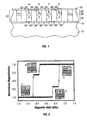
- FIG. 1is a schematic sectional view of the patterned multilevel perpendicular magnetic recording medium according to the present invention.
- FIG. 2is a magneto-optical Kerr effect (MOKE) hysteresis loop of an unpatterned section of the magnetic recording medium showing schematic representations of the four possible magnetization levels (labeled as A, B, C, and D) of the cells in a magnetic island.
- MOKEmagneto-optical Kerr effect
- FIG. 3is a readback signal of the patterned multilevel media after dc magnetizing the sample (top) and after applying a square wave write pattern (middle), and showing a schematic representation of the cell magnetizations corresponding to the readback signal (bottom).
- FIG. 4is a schematic illustrating the method in which an inductive write head writes the four different magnetization levels in a magnetic island of the patterned multilevel media.
- FIG. 5is a schematic illustrating the method in which an inductive write head with an electrically resistive heater writes the four different magnetization levels in a magnetic island of the patterned multilevel media.
- FIG. 6is a top view of a disk drive embodiment of the multilevel magnetic recording system showing the magnetic islands as dots on concentric tracks of the recording disk.
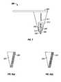
- FIG. 7is a sectional view of one type of magnetic force microscopy (MFM) probe as an inductive write head for the multilevel magnetic recording system.
- MFMmagnetic force microscopy
- FIGS. 8 ( a ) and 8 ( b )show the two different magnetizations of the probe tip of the MFM probe type inductive head shown in FIG. 7 .
- FIG. 9is a view of a scanning probe embodiment of the multilevel magnetic recording system showing an x-y array of MFM probe inductive write heads and the media substrate with the magnetic islands arranged as an x-y array, the islands being represented as dots.
- FIG. 1is a schematic of the patterned magnetic recording medium according to the present invention.
- the mediumincludes a substrate 12 , a multilevel perpendicular magnetic recording layer 50 , an optional underlayer 14 and optional protective overcoat 16 .
- the recording layer 50includes a plurality of islands, such as representative islands 52 , 54 , 56 , 58 , spaced-apart by spaces 60 .
- Each islandis formed of a first layer 20 of magnetic material with perpendicular magnetic anisotropy, a second layer 40 of magnetic material with perpendicular magnetic anisotropy and a spacer layer 30 that separates and magnetically decouples the two magnetic layers 20 , 40 in each island.
- Each islandis thus a multilevel magnetic island with at least two stacked magnetically decoupled cells, such as cells 22 , 32 in island 52 .
- Each cellis a single magnetic domain and is separated from the other cell in its island by the spacer layer 30 and from the cells in other islands by the regions depicted as spaces 60 .
- the spaces 60define the regions between the magnetic islands and are typically formed of nonmagnetic material, but may be formed of ferromagnetic material provided the material does not adversely affect the signal recording and detection from the magnetic islands that they separate.
- the magnetic islandscan be formed by first lithographically patterning the substrate, depositing the layers making up recording layer 50 over the patterned resist and then removing the resist, leaving the magnetic islands.
- the magnetic islandscan be formed by first depositing the layers making up recording layer 50 on the substrate, lithographically patterning the recording layer, etching the recording layer through the lithographic mask, and then removing the resist, leaving the magnetic islands.
- the spaces 60 in the regions between the islandsare voids that may be filled with nonmagnetic material, such as alumina or spin-on glass.
- a substantially planar surface topographycan then be formed. The process would involve first forming the magnetic islands, then depositing alumina to a thickness greater than that required to fill the spaces 60 , and then polishing the alumina with a chemical-mechanical polish (CMP) process until the magnetic islands were just exposed. This leaves the alumina in the spaces 60 and the tops of the magnetic islands approximately coplanar.
- CMPchemical-mechanical polish
- each magnetic state in the two-layer embodiment of FIG. 1can thus be represented as a two-bit byte or word. If the cells in the lower layer 20 are selected as the first bit in the byte or word and magnetization in the up direction is considered a 0, then the magnetic states are as follows:
- FIG. 1is depicted with two magnetic layers, but 3 or more magnetic layers are possible.
- the total readback signal integrated over the n different magnetic layersgives rise to 2 n different signal levels, which can be used for magnetic recording.
- the recording densityis thus increased by a factor of 2 (n-1) .
- a magnetic thin filmwas sputter-deposited at room temperature onto an hexagonal array of SiO 2 pillars with a diameter of 150 nm and a height of 80 nm. The spacing between the center of the pillars was 300 nm.
- the pillarswere formed by lithographically patterning a SiO 2 film formed on a Si substrate.
- the structurehad two perpendicular Co/Pd multilayers separated by a 5 nm thick Pd layer to magnetically decouple the upper and lower multilayers.
- the composition of the filmwas as follows:
- the multilayer of 10 Co/Pd pairsis the lower magnetic layer 20
- the multilayer of 6 Co/Pd pairsis the upper magnetic layer 40
- the 5 nm thick Pd layeris the spacer layer 30 .
- the strength of the magnetic anisotropy and coercivity of the magnetic layerscan be easily altered by changing the Co and Pd thicknesses.
- all of the layers making up layers 20 , 30 and 40were also deposited into the regions or “trenches” in the SiO 2 between the pillars of SiO 2 .
- the magnetic properties of the islandsare not affected by the magnetic material in the trenches and there are thus voids between the magnetic islands.
- MOKEMagneto-optical Kerr effect
- a magnetic recording experimentwas also performed on this island array structure.
- the structurewas fixed on a x-y stage, controlled by piezoelectric drivers with a resolution of less than 2 nm, and scanned at low velocity (approximately 5 ⁇ m/s) while in physical contact with the recording head.
- a conventional longitudinal recording giant magnetoresistive (GMR) read/write headwas used with write and read head widths of about 240 nm and 180 nm, respectively.
- the structurewas first dc magnetized in an external perpendicular field of 20 kOe. The recording head was then aligned parallel to the rows of magnetic islands.
- writing on patterned mediarequires the synchronization of the square wave write pattern with the island pattern.
- the island locationscan be easily retrieved from the readback signal of the dc-erased magnetized islands, where the minima indicate the trenches or spaces separating the islands, as shown by the top signal in FIG. 3 .
- the read head width of about 180 nmenables the signal to be read back from an individual island in the array.
- a horizontal write headwas used with a fixed write current of 40 mA.
- the magnetic cellscan be formed of a granular polycrystalline cobalt-chromium (CoCr) alloy grown on a special growth-enhancing sublayer that induces the crystalline C-axis to be perpendicular to the plane of the layer, so that the layer has strong perpendicular magnetocrystalline anisotropy.
- Materials that may be used as the growth-enhancing sublayer for the CoCr granular layerinclude Ti, TiCr, C, NiAl, SiO 2 and CoCr, where Cr is about 35-40 atomic percent.
- the magnetic cellscan also be formed any of the known amorphous materials that exhibit perpendicular magnetic anisotropy, such as CoSm, TbFe, TbFeCo, and GdFe alloys.
- the magnetic cellscan also be formed of chemically ordered CoPt, CoPd, FePt, FePd, CoPt 3 or CoPd 3 .
- Chemically-ordered alloys of CoPt, CoPd, FePt or FePd, in their bulk form,are known as face-centered tetragonal (FCT) L1 0 -ordered phase materials (also called CuAu materials). They are known for their high magnetocrystalline anisotropy and magnetic moment.
- FCTface-centered tetragonal
- L1 0 -ordered phase materialsalso called CuAu materials
- Theyare known for their high magnetocrystalline anisotropy and magnetic moment.
- the c-axis of the L1 0 phaseis the easy axis of magnetization and is oriented perpendicular to the substrate, thus making the material suitable for perpendicular magnetic recording media.
- these layershave very strong perpendicular anisotropy.
- a “soft” magnetically permeable underlayeris often used on the substrate beneath the magnetic layer to provide a flux return path for the field from the read/write pole head.
- a soft underlayermay not be necessary. Alloy materials that are suitable for the soft underlayer include NiFe, FeAlSi, FeTaN, FeN, CoFeB and CoZrNb.
- FIG. 4illustrates the manner in which the inductive write head 100 records each of the four possible magnetic states in a magnetic island having two single domain magnetic cells.
- the head 100is a perpendicular head and has a coil 102 connected to a current source 104 .
- the current source 104is part of the write driver circuitry that also includes switching circuitry to generate bi-directional write pulses with at least two different current levels, I 1 and I 2 .
- the write currentgenerates a generally perpendicular magnetic field from the write pole 105 that returns back to the return pole 107 .
- the lower magnetic layer 20has a higher coercivity than the upper magnetic layer 40 .
- Current level I 1generates a magnetic write field greater than the coercivity of the lower layer 20 .
- a positive I 1changes the magnetization direction in both layers 20 , 40 and generates the A state.
- a negative I 1 write pulsechanges the magnetization direction in both layers 20 , 40 and generates the C state.
- the islandTo generate the D state, the island must first be in the A state, after which a second current pulse with a value of I 2 in the “negative” direction is applied, as shown in FIG. 4 ( c ).
- This negative I 2 current pulsegenerates a magnetic write field greater than the coercivity of the upper layer 40 but less than the coercivity of the lower layer 20 so only the magnetization of only the upper layer 40 is switched.
- the islandmust first be in the C state, after which a second current pulse with a value of I 2 in the “positive” direction is applied, as shown in FIG. 4 ( d ).
- This positive I 2 current pulsegenerates a magnetic write field greater than the coercivity of the upper layer 40 but less than the coercivity of the lower layer 20 so only the magnetization of the upper layer 40 is switched.
- a substantial difference in coercivity between the magnetic layersassures that only the upper cell in the magnetic island is switched when the I 2 pulse is applied.
- the coercivities in the two cells in an islandcan be very close or the coercivity of the lower cell only slightly greater than the coercivity of the upper cell if the media is designed so that the lower cell is sufficiently far from the upper cell.
- the thickness of the spacer layer 30the lower layer 40 will be exposed to a much lower write field than the upper layer 20 when the I 2 pulse is applied.
- FIG. 5illustrates the manner in which a thermally-assisted inductive write head 100 ′ records each of the four possible magnetic states in a magnetic island having two single domain magnetic cells.
- the head 100 ′is a perpendicular head and has a coil 102 connected to a current source 104 that provides a fixed write current I 0 .
- the current source 104is part of the write driver circuitry that also includes switching circuitry to generate bi-directional write pulses with plus or minus current levels, I 0 .
- the head 100 ′also includes an electrically resistive heater 103 located between the write pole 105 and the return pole 107 .
- the heater 103is connected to circuitry for applying current pulses that enable the heater 103 to generate heat pulses to the magnetic islands on the medium.
- Pat. No. 6,493,183describes an inductive write head for generating the magnetic write field and a heater for heating the media.
- the write current I 0generates a generally perpendicular magnetic field from the write pole 105 that returns back to the return pole 107 .
- the lower magnetic layer 20has a higher coercivity than the upper magnetic layer 40 .
- Current level I 0generates a magnetic write field greater than the coercivity of the upper layer 40 but less than the coercivity of the lower layer 20 .
- the islandTo generate the D state, the island must first be in the A state, after which a negative I 0 current pulse is applied, as shown in FIG. 5 ( c ). This negative I 0 current pulse generates a magnetic write field greater than the coercivity of the upper layer 40 but less than the coercivity of the lower layer 20 so only the magnetization of the upper layer 40 is switched.
- the islandTo generate the B state, the island must first be in the C state, after which a positive I 0 current pulse is applied, as shown in FIG. 5 ( d ). This positive I 0 current pulse generates a magnetic write field greater than the coercivity of the upper layer 40 but less than the coercivity of the lower layer 20 so only the magnetization of the upper layer 40 is switched.
- a substantial difference in coercivity between the magnetic layersassures that only the upper cell in the magnetic island is switched when the I 0 pulse is applied.
- the coercivities in the two cells in an islandcan be very close or the coercivity of the lower cell only slightly greater than the coercivity of the upper cell if the media is designed so that the lower cell is sufficiently far from the upper cell.
- the thickness of the spacer layer 30the lower layer 40 will be exposed to a much lower write field than the upper layer 20 when the I 0 pulse is applied.
- the lower layercan be formed of a 6 [Co(4 ⁇ )/Pd(10 ⁇ )] multilayer and have a coercivity of approximately 3000 Oe
- the upper layercan be formed of a 6 [Co(2.5 ⁇ )/Pd(5 ⁇ )] multilayer and have a coercivity of approximately 2000 Oe.
- a fixed write current pulse of 10 mAwill generate a magnetic write field of approximately 3000 Oe.
- a heat pulse of a few milliwattswill increase the temperature of both layers by approximately 40 K, which will reduce the coercivity of the lower layer to approximately 1000 Oe.
- FIG. 5shows the heater 103 located between the poles 105 , 107
- the heatermay also be located on either side of a pole.
- the heatermay be formed as part of the coil of a longitudinal write head, as described in published U.S. Patent Application 2003/0021191A1, in which case portions of the coil serve as the electrical leads to the heater.
- the heaterdoes not need to be an electrically resistive heater and may be a separate element not directly associated with the inductive write head, such as a laser that directs a light spot to the medium, provided the heat pulse and the magnetic write field can be localized to assure that only the desired cells have their magnetizations switched.
- FIG. 6is a top view of a disk drive embodiment of the multilevel magnetic recording system according to the present invention.
- the drive 200has a housing or base 212 that supports an actuator 230 and a drive motor for rotating the multilevel magnetic recording disk 214 .
- the disk 214 substratemay be any suitable substrate, such as the glass or aluminum-magnesium (AlMg) substrates used in conventional disk drives.
- the actuator 230may be a voice coil motor (VCM) rotary actuator that has a rigid arm 234 and rotates about pivot 232 as shown by arrow 224 .
- VCMvoice coil motor
- a head-suspension assembly 220includes a suspension 221 that has one end attached to the end of actuator arm 234 and a head carrier 222 , such as an air-bearing slider, attached to the other end of suspension 221 .
- the magnetic islands 215 on disk 214are arranged in radially-spaced circular tracks 218 .
- the movement of actuator 230allows the head 100 on the trailing end of head carrier 222 to access different data tracks 218 on disk 214 for the recording of multilevel data in the magnetic islands 215 .
- the writing on patterned mediarequires the synchronization of the write pulses with the island pattern.
- the inductive write head used to record the signal shown in FIG. 3was a conventional longitudinal inductive write head, and the inductive write head depicted in FIG. 4 is a perpendicular head with a write pole and a return pole.
- Another type of inductive write head for use in the present inventionis based on a magnetic-force-microscopy (MFM) probe comprising a cantilever with a nanometer-sharp magnetic tip at the cantilever end.
- MFMmagnetic-force-microscopy
- FIG. 7is a side sectional view of the probe 300 showing the probe body 310 attached to cantilever 350 .
- the probe body 310has a pair of poles 340 , 342 and an inductive coil 311 .
- the coil 311 and poles 340 , 342are formed using conventional lithographic techniques, as is well known in the manufacture of disk drive thin film inductive write heads in which the coil and poles are formed on the trailing end of a conventional disk dbrive air-bearing slider.
- the poles 340 , 342are spaced apart by a nonmagnetic gap 314 .
- the poles 340 , 342are interconnected to form a yoke through which the coil 311 passes.
- the sectioned ends of the coil windingsare shown in end view as coil 311 .
- a probe tip 320which is formed in contact with at least one of the poles 340 or 342 and preferably also in contact with the end surface of the gap 314 , extends from the ends of the poles.
- the probe tip 320has at least one surface or side 322 which is in contact with one of the poles and is formed of a magnetic material.
- the probe tip 320is shown as having a generally conical shape, but its actual shape can vary. As an alternative to the yoke structure depicted in FIG.
- the coilmay be wrapped in a helical manner around probe tip 320 , the probe body 310 , or the cantilever 350 provided these structures are formed of material that allows the magnetic field generated by the coil to be directed to the magnetic probe tip 320 .
- This type of MFM probeis described in U.S. Pat. No. 5,436,448.
- the coilreceives current I 1 or I 2 from the write driver, which causes probe tip 320 to be magnetized in one direction with a field strength determined by the value of I 1 or I 2 .
- the direction of magnetization of the probe tipis reversed.
- These two possible magnetization directions and two possible magnetic field valuesenable the four possible magnetic states (A, B, C, D) to be written in the magnetic islands in the same manner as described with respect to FIG. 4 .
- the cantilever 350 with probe tip 320is attached to the actuator arm 234 (FIG. 5 ).
- the actuator arm 234FIG. 5
- Another type of actuator that enables the MFM probe to be used in a disk driveis described in U.S. Pat. No. 5,804,710.
- the MFM probe type of inductive write headalso permits multilevel magnetic recording in a scanning probe system.
- a scanning probe systemis described in “Millipede-A MEMS-Based Scanning-Probe Data-Storage System”, IEEE Transactions on Magnetics , Vol. 39, No. 2, March 2003, pp. 938-945.
- the “Millipede” systemis a thermomechanical system in which the data is recorded by heating the probe tips to cause pits in a polymeric storage medium.
- the scanning probe embodiment of the multilevel magnetic recording system according to the present inventionis shown in FIG. 9 .
- the multilevel magnetic recording medium 400is as described with respect to FIG. 1 and includes the substrate 401 and the magnetic islands 402 .
- the islands 402are arranged as an x-y array of mutually perpendicular rows on the substrate 401 .
- the substrate 401is supported on a platform 402 of an xyz scanner.
- An array of MFM type probe tips 410 with associated cantilevers 411is fabricated on a chip 420 .
- the chip 420 and medium 400are movable relative to one another in the x-y directions by the xyz scanner. Thus each probe is associated with only a section of the total island array and addresses only the islands in that section.
- Multiplex drivers (MUX) 430 , 432allow write currents I 1 , I 2 to be delivered to each MFM probe individually.
- the scanning probe system described above and depicted in FIG. 9has an array of probes.
- the scanning probe multilevel magnetic recording system according to the present inventionis also possible with only a single probe in cooperation with an xyz scanner, in the manner of a conventional MFM system.
Landscapes
- Engineering & Computer Science (AREA)
- Computer Hardware Design (AREA)
- Manufacturing & Machinery (AREA)
- Magnetic Record Carriers (AREA)
- Peptides Or Proteins (AREA)
- Enzymes And Modification Thereof (AREA)
Abstract
Description
- “MAGNETIC RECORDING SYSTEM WITH PATTERNED MULTILEVEL PERPENDICULAR MAGNETIC RECORDING MEDIA” application Ser. No. 10/727,812 filed Dec. 3, 2003; and “METHOD FOR MAGNETIC RECORDING ON PATTERNED MULTILEVEL PERPENDICULAR MEDIA USING VARIABLE WRITE CURRENT” application Ser. No. 10/727,812 filed Dec. 3, 2003; and “METHOD FOR MAGNETIC RECORDING ON PATTERNED MULTILEVEL PERPENDICULAR MEDIA USING THERMAL ASSISTANCE AND FIXED WRITE CURRENT ” application Ser. No. 10/728,213 Dec. 3, 2003.
- C(40 Å)/Pd(10 Å)/[Co(3.3 Å)/Pd(8.3 Å)]6/Pd(50 Å)/[Co(2.5 Å)/Pd(6.5 Å)]10/Pd(20Å)/SiO2
Claims (36)
Priority Applications (8)
| Application Number | Priority Date | Filing Date | Title |
|---|---|---|---|
| US10/727,826US6947235B2 (en) | 2003-12-03 | 2003-12-03 | Patterned multilevel perpendicular magnetic recording media |
| TW093129668ATW200521997A (en) | 2003-12-03 | 2004-09-30 | Patterned multilevel perpendicular magnetic recording media |
| EP04021484AEP1542209B1 (en) | 2003-12-03 | 2004-11-03 | Magnetic recording medium |
| DE602004009392TDE602004009392T2 (en) | 2003-12-03 | 2004-11-03 | Magnetic recording medium |
| JP2004324802AJP2005166238A (en) | 2003-12-03 | 2004-11-09 | Patterned multilevel perpendicular magnetic recording media |
| CNB2004100946541ACN100414609C (en) | 2003-12-03 | 2004-11-11 | Patterned Multilayer Perpendicular Magnetic Recording Media |
| KR1020040098987AKR20050053496A (en) | 2003-12-03 | 2004-11-30 | Patterned multilevel perpendicular magnetic recording media |
| SG200407007ASG112073A1 (en) | 2003-12-03 | 2004-12-02 | Patterned multilevel perpendicular magnetic recording media |
Applications Claiming Priority (1)
| Application Number | Priority Date | Filing Date | Title |
|---|---|---|---|
| US10/727,826US6947235B2 (en) | 2003-12-03 | 2003-12-03 | Patterned multilevel perpendicular magnetic recording media |
Publications (2)
| Publication Number | Publication Date |
|---|---|
| US20050122609A1 US20050122609A1 (en) | 2005-06-09 |
| US6947235B2true US6947235B2 (en) | 2005-09-20 |
Family
ID=34523002
Family Applications (1)
| Application Number | Title | Priority Date | Filing Date |
|---|---|---|---|
| US10/727,826Expired - LifetimeUS6947235B2 (en) | 2003-12-03 | 2003-12-03 | Patterned multilevel perpendicular magnetic recording media |
Country Status (8)
| Country | Link |
|---|---|
| US (1) | US6947235B2 (en) |
| EP (1) | EP1542209B1 (en) |
| JP (1) | JP2005166238A (en) |
| KR (1) | KR20050053496A (en) |
| CN (1) | CN100414609C (en) |
| DE (1) | DE602004009392T2 (en) |
| SG (1) | SG112073A1 (en) |
| TW (1) | TW200521997A (en) |
Cited By (41)
| Publication number | Priority date | Publication date | Assignee | Title |
|---|---|---|---|---|
| US20050117242A1 (en)* | 2003-11-28 | 2005-06-02 | Kabushiki Kaisha Toshiba | Perpendicular magnetic head and perpendicular magnetic disk apparatus |
| US20050249870A1 (en)* | 2004-04-09 | 2005-11-10 | Fuji Electric Holdings Co., Ltd. | Method for producing multilayer film perpendicular magnetic recording medium |
| US20060092541A1 (en)* | 2004-10-29 | 2006-05-04 | Andreas Moser | Magnetic recording disk drive with patterned media and circuit for generating timing pulses from the pattern |
| US7050256B1 (en)* | 2004-06-29 | 2006-05-23 | The United States Of America As Represented By The Administrator Of The National Aeronautics And Space Administration | Fast erase method and apparatus for digital media |
| US20060280975A1 (en)* | 2005-06-09 | 2006-12-14 | Albrecht Thomas R | Magnetic recording disk with patterned nondata islands of alternating polarity |
| US20070259210A1 (en)* | 2006-05-02 | 2007-11-08 | Canon Kabushiki Kaisha | Structure and process for production thereof |
| US20080085425A1 (en)* | 2006-10-10 | 2008-04-10 | Seagate Technology Llc | Bit patterned magnetic media with exchange coupling between bits |
| US20080085424A1 (en)* | 2006-10-10 | 2008-04-10 | Seagate Technology Llc | Single-pass recording of multilevel patterned media |
| US20080094742A1 (en)* | 2006-10-19 | 2008-04-24 | Thomas Robert Albrecht | Servo patterns for patterned media |
| US20080106821A1 (en)* | 2006-11-03 | 2008-05-08 | Samsung Electronics Co., Ltd. | Patterned magnetic recording medium |
| US20080239542A1 (en)* | 2007-03-30 | 2008-10-02 | Kabushiki Kaisha Toshiba | Magnetic recording head and magnetic recording method |
| US20080292907A1 (en)* | 2007-05-22 | 2008-11-27 | Hitachi Global Storage Technologies Netherlands B.V. | Patterned perpendicular magnetic recording medium with exchange coupled recording layer structure and magnetic recording system using the medium |
| US20090002865A1 (en)* | 2007-06-28 | 2009-01-01 | Seagate Technology Llc | Zone Based Timing Recovery For Bit Patterned Media |
| US20090080109A1 (en)* | 2007-09-26 | 2009-03-26 | Kabushiki Kaisha Toshiba | Magnetic recording device |
| US20090135527A1 (en)* | 2007-11-23 | 2009-05-28 | Samsung Electronics Co., Ltd. | Magnetic recording media and method of fabricating the same |
| US20090154017A1 (en)* | 2007-12-17 | 2009-06-18 | Hitachi Global Storage Technologies Netherlands Bv | System, method and apparatus for patterned media with reduced magnetic trench material |
| US20090155627A1 (en)* | 2007-12-14 | 2009-06-18 | Hitachi Global Storage Technologies Netherlands B.V. | Discrete track media with a capped media structure having high moment and exchange |
| US20090199768A1 (en)* | 2008-02-12 | 2009-08-13 | Steven Verhaverbeke | Magnetic domain patterning using plasma ion implantation |
| US20090201722A1 (en)* | 2008-02-12 | 2009-08-13 | Kamesh Giridhar | Method including magnetic domain patterning using plasma ion implantation for mram fabrication |
| US20100020435A1 (en)* | 2008-07-25 | 2010-01-28 | Agency For Science, Technology And Research | Recording device with write head spanning multiple rows of bit cells and multi-sensor read head |
| US20100061018A1 (en)* | 2008-09-11 | 2010-03-11 | Hitachi Global Storage Technologies Netherlands B.V. | Magnetic recording disk drive with patterned media and optical system for clocking write data |
| US20100073814A1 (en)* | 2008-09-24 | 2010-03-25 | Pierre-Olivier Jubert | Writing and reading multi-layer continuous magnetic recording media |
| US20100091618A1 (en)* | 2008-10-09 | 2010-04-15 | Hitachi Global Storage Technologies Netherlands B.V. | Patterned-media magnetic recording disk with optical contrast enhancement and disk drive using optical contrast for write synchronization |
| US20100098873A1 (en)* | 2008-10-22 | 2010-04-22 | Applied Materials, Inc. | Patterning of magnetic thin film using energized ions |
| US20100096256A1 (en)* | 2008-02-12 | 2010-04-22 | Omkaram Nalamasu | Patterning of magnetic thin film using energized ions and thermal excitation |
| US20100110579A1 (en)* | 2008-10-30 | 2010-05-06 | Vitaliy Lomakin | Apparatus, System and Method for Magnetic Recording |
| US20100238584A1 (en)* | 2009-03-23 | 2010-09-23 | Messner William C | Simultaneous bit pattern determination and head positional information detection on patterned media |
| US20100284104A1 (en)* | 2007-11-26 | 2010-11-11 | Commissariat A I'energie Atomique Et Aux Energies Alternatives | Magnetic recording medium |
| US20100302669A1 (en)* | 2009-05-28 | 2010-12-02 | Seagate Technology Llc | Transducer design with a sensor close to write pole |
| US7876529B1 (en) | 2005-11-03 | 2011-01-25 | Seagate Technology Llc | Recording disk with antiferromagnetically coupled multilayer ferromagnetic island disposed in trench between discrete tracks |
| US20110019305A1 (en)* | 2009-07-27 | 2011-01-27 | Suess Dieter | Magnetic storage device |
| US20110085264A1 (en)* | 2009-10-12 | 2011-04-14 | Hitachi Global Storage Technologies Netherlands B.V. | Patterned perpendicular magnetic recording medium with data islands having a flux channeling layer below the recording layer |
| US20110109987A1 (en)* | 2009-11-10 | 2011-05-12 | International Business Machines Corporation | Writing and reading multi-level patterned magnetic recording media, with more than two recording levels |
| US20110109984A1 (en)* | 2009-11-10 | 2011-05-12 | International Business Machines Corporation | Writing and reading multi-layer continuous magnetic recording media, with more than two recording layers |
| US20110134560A1 (en)* | 2008-09-25 | 2011-06-09 | International Business Machines Corporation | Writing and reading multi-level patterned magnetic recording media |
| US7998333B1 (en) | 2006-09-21 | 2011-08-16 | Canon Kabushiki Kaisha | Method of manufacturing a magnetic recoding medium |
| US20140093747A1 (en)* | 2012-09-28 | 2014-04-03 | HGST Netherlands B.V. | Magnetic recording medium with anti-ferromagnetically coupled magnetic layers |
| US20150243303A1 (en)* | 2006-04-06 | 2015-08-27 | Sigma Pro Ltd. Llc | Magnetic Storage Medium Comprised of Magnetic Nanoparticles Contained Within Nanotubes |
| US9183870B2 (en) | 2007-12-07 | 2015-11-10 | Wisconsin Alumni Research Foundation | Density multiplication and improved lithography by directed block copolymer assembly |
| US10672425B2 (en) | 2017-06-27 | 2020-06-02 | Western Digital Technologies, Inc. | Embedded disconnected circuits in magnetic storage media of data storage devices |
| US11495249B1 (en) | 2021-04-12 | 2022-11-08 | Seagate Technology Llc | Method and apparatus for magnetically recording data with three or more states per unit of data |
Families Citing this family (17)
| Publication number | Priority date | Publication date | Assignee | Title |
|---|---|---|---|---|
| KR100754397B1 (en)* | 2006-02-22 | 2007-08-31 | 삼성전자주식회사 | Magnetic Memory Using Magnetic Domain Movement |
| JP2008084432A (en)* | 2006-09-27 | 2008-04-10 | Hoya Corp | Magnetic recording medium and manufacturing method of magnetic recording medium |
| US7732071B2 (en)* | 2006-11-10 | 2010-06-08 | Hitachi Global Storage Technologies Netherlands B.V. | Perpendicular magnetic recording system with patterned medium and manufacturing process for the medium |
| US7826171B2 (en) | 2007-01-23 | 2010-11-02 | Seagate Technology Llc | Interconnect architecture for disc drive array |
| US7957091B2 (en)* | 2007-01-23 | 2011-06-07 | Seagate Technology Llc | Recordable disc with fluid bearing features |
| US7800865B2 (en)* | 2007-01-23 | 2010-09-21 | Seagate Technology Llc | Disc drive head actuator |
| US7965589B2 (en)* | 2007-01-23 | 2011-06-21 | Seagate Technology Llc | Recordable disc and motor |
| US7835110B2 (en)* | 2007-01-23 | 2010-11-16 | Seagate Technology | MEMS disc drive |
| US7489472B2 (en)* | 2007-01-24 | 2009-02-10 | Maxtor Corporation | High-order hybrid actuator controller |
| US8076013B2 (en) | 2007-02-13 | 2011-12-13 | Wd Media (Singapore) Pte. Ltd. | Magnetic recording medium, magnetic recording medium manufacturing method, and magnetic disk |
| US7670696B2 (en)* | 2007-05-01 | 2010-03-02 | Hitachi Global Storage Technologies Netherlands B.V. | Perpendicular magnetic recording medium with patterned magnetic islands and nonmagnetic trenches and manufacturing method for suppressing surface diffusion of trench material |
| US7867406B2 (en)* | 2007-12-26 | 2011-01-11 | Hitachi Global Storage Technologies Netherlands, B.V. | Patterned magnetic media having an exchange bridge structure connecting islands |
| US8449730B2 (en) | 2009-07-20 | 2013-05-28 | Carnegie Mellon University | Buffer layers for L10 thin film perpendicular media |
| US8023214B2 (en)* | 2009-09-10 | 2011-09-20 | Tdk Corporation | Rework method and apparatus of magnetic record medium, information |
| CN104502635B (en)* | 2014-12-22 | 2018-05-01 | 长春理工大学 | A kind of magnetic force microscopy difference magnetic force micro imaging method |
| CN105698929B (en)* | 2016-02-29 | 2019-06-28 | 苏州宏策光电科技有限公司 | Nitrogen reactive sputtering prepares CoCr/Sb multiplayer films in EUV artificial lens monochromator and production method |
| CN105698928B (en)* | 2016-02-29 | 2018-04-17 | 苏州宏策光电科技有限公司 | Nitrogen reactive sputtering prepares CoCr/Ti multiplayer films in EUV artificial lens monochromators and production method |
Citations (27)
| Publication number | Priority date | Publication date | Assignee | Title |
|---|---|---|---|---|
| US3655441A (en) | 1966-08-22 | 1972-04-11 | Honeywell Inc | Electroless plating of filamentary magnetic records |
| US5436448A (en) | 1992-01-10 | 1995-07-25 | Hitachi, Ltd. | Surface observing apparatus and method |
| US5458987A (en)* | 1985-06-11 | 1995-10-17 | Nikon Corporation | Multilayered magnetooptical recording medium |
| US5583727A (en) | 1995-05-15 | 1996-12-10 | International Business Machines Corporation | Multiple data layer magnetic recording data storage system with digital magnetoresistive read sensor |
| US5804710A (en) | 1997-06-05 | 1998-09-08 | International Business Machines Corporation | Atomic force microscope system with multi-directional voice coil actuator for controlling the stylus |
| US5820769A (en)* | 1995-05-24 | 1998-10-13 | Regents Of The University Of Minnesota | Method for making magnetic storage having discrete elements with quantized magnetic moments |
| US5844755A (en)* | 1994-12-22 | 1998-12-01 | Oki Electric Industry Co., Ltd. | Giant magnetoresistive information recording medium, and associated recording and reproducing method and apparatus |
| US5900729A (en) | 1997-03-20 | 1999-05-04 | International Business Machines Corporation | Magnetic force microscopy probe with integrated coil |
| US5900728A (en) | 1997-03-20 | 1999-05-04 | International Business Machines Corporation | Alternating current magnetic force microscopy system with probe having integrated coil |
| US6011664A (en) | 1995-08-31 | 2000-01-04 | Carnegie Mellon University | Techniques for ultrahigh density writing with a probe on erasable magnetic media |
| US6171676B1 (en)* | 1996-03-19 | 2001-01-09 | Fujitsu Limited | Magnetic recording medium containing fine magnetic crystal grains and its manufacture |
| US6174597B1 (en)* | 1996-07-26 | 2001-01-16 | Kabushiki Kaisha Toshiba | Magnetic recording apparatus |
| US6331364B1 (en) | 1999-07-09 | 2001-12-18 | International Business Machines Corporation | Patterned magnetic recording media containing chemically-ordered FePt of CoPt |
| US20020037439A1 (en) | 2000-09-27 | 2002-03-28 | Dmitri Litvinov | Multilayer magnetic recording media with columnar microstructure for improved exchange decoupling |
| US6383597B1 (en) | 2000-06-21 | 2002-05-07 | International Business Machines Corporation | Magnetic recording media with magnetic bit regions patterned by ion irradiation |
| US6391430B1 (en)* | 2000-06-21 | 2002-05-21 | International Business Machines Corporation | Patterned magnetic recording media with discrete magnetic regions separated by regions of antiferromagnetically coupled films |
| US6421195B1 (en)* | 1999-09-20 | 2002-07-16 | International Business Machines Corporation | Magnetic disk media with patterned sections |
| US6493183B1 (en) | 2000-06-29 | 2002-12-10 | International Business Machines Corporation | Thermally-assisted magnetic recording system with head having resistive heater in write gap |
| US20030021191A1 (en) | 2001-07-25 | 2003-01-30 | Yimin Hsu | Magnetic recording system with single coil for thermally assisted writing |
| US20030091865A1 (en) | 2001-11-09 | 2003-05-15 | Yunjie Chen | Manufacturing method for high-density magnetic data storage media |
| US20030107833A1 (en) | 2001-10-26 | 2003-06-12 | Rettner Charles T. | Patterned media magnetic recording disk drive with timing of write pulses by sensing the patterned media |
| US6660357B1 (en)* | 2000-02-04 | 2003-12-09 | Seagate Technology Llc | Perpendicular magnetic recording media with laminated soft magnetic underlayer |
| US20040080847A1 (en)* | 2002-10-29 | 2004-04-29 | Imation Corp. | Perpendicular patterned magnetic media |
| US6737172B1 (en)* | 2000-12-07 | 2004-05-18 | Seagate Technology Llc | Multi-layered anti-ferromagnetically coupled magnetic media |
| US20040265639A1 (en)* | 2003-06-30 | 2004-12-30 | Imation Corp. | NiCr and NiFeCr seed layers for perpendicular magnetic recording media |
| US6865044B1 (en)* | 2003-12-03 | 2005-03-08 | Hitachi Global Storage Technologies Netherlands B.V. | Method for magnetic recording on patterned multilevel perpendicular media using thermal assistance and fixed write current |
| US6882488B1 (en)* | 2003-12-03 | 2005-04-19 | Hitachi Global Storage Technologies Netherlands B.V. | Method for magnetic recording on patterned multilevel perpendicular media using variable write current |
Family Cites Families (4)
| Publication number | Priority date | Publication date | Assignee | Title |
|---|---|---|---|---|
| US6214434B1 (en)* | 1997-09-02 | 2001-04-10 | Seagate Technology Llc | Isolated single-domain high-density magnetic recording media and method of manufacturing the media |
| US6650513B2 (en)* | 2001-01-29 | 2003-11-18 | International Business Machines Corporation | Magnetic devices with a ferromagnetic layer having perpendicular magnetic anisotropy and an antiferromagnetic layer for perpendicularly exchange biasing the ferromagnetic layer |
| JP2003196815A (en)* | 2001-10-16 | 2003-07-11 | Canon Inc | Magnetic recording media |
| JP3789101B2 (en)* | 2002-03-26 | 2006-06-21 | 株式会社東芝 | Magnetic recording apparatus and magnetic recording writing method |
- 2003
- 2003-12-03USUS10/727,826patent/US6947235B2/ennot_activeExpired - Lifetime
- 2004
- 2004-09-30TWTW093129668Apatent/TW200521997A/enunknown
- 2004-11-03EPEP04021484Apatent/EP1542209B1/ennot_activeExpired - Lifetime
- 2004-11-03DEDE602004009392Tpatent/DE602004009392T2/ennot_activeExpired - Fee Related
- 2004-11-09JPJP2004324802Apatent/JP2005166238A/ennot_activeWithdrawn
- 2004-11-11CNCNB2004100946541Apatent/CN100414609C/ennot_activeExpired - Fee Related
- 2004-11-30KRKR1020040098987Apatent/KR20050053496A/ennot_activeWithdrawn
- 2004-12-02SGSG200407007Apatent/SG112073A1/enunknown
Patent Citations (28)
| Publication number | Priority date | Publication date | Assignee | Title |
|---|---|---|---|---|
| US3655441A (en) | 1966-08-22 | 1972-04-11 | Honeywell Inc | Electroless plating of filamentary magnetic records |
| US5458987A (en)* | 1985-06-11 | 1995-10-17 | Nikon Corporation | Multilayered magnetooptical recording medium |
| US5436448A (en) | 1992-01-10 | 1995-07-25 | Hitachi, Ltd. | Surface observing apparatus and method |
| US5844755A (en)* | 1994-12-22 | 1998-12-01 | Oki Electric Industry Co., Ltd. | Giant magnetoresistive information recording medium, and associated recording and reproducing method and apparatus |
| US5583727A (en) | 1995-05-15 | 1996-12-10 | International Business Machines Corporation | Multiple data layer magnetic recording data storage system with digital magnetoresistive read sensor |
| US5820769A (en)* | 1995-05-24 | 1998-10-13 | Regents Of The University Of Minnesota | Method for making magnetic storage having discrete elements with quantized magnetic moments |
| US6011664A (en) | 1995-08-31 | 2000-01-04 | Carnegie Mellon University | Techniques for ultrahigh density writing with a probe on erasable magnetic media |
| US6171676B1 (en)* | 1996-03-19 | 2001-01-09 | Fujitsu Limited | Magnetic recording medium containing fine magnetic crystal grains and its manufacture |
| US6174597B1 (en)* | 1996-07-26 | 2001-01-16 | Kabushiki Kaisha Toshiba | Magnetic recording apparatus |
| US5900729A (en) | 1997-03-20 | 1999-05-04 | International Business Machines Corporation | Magnetic force microscopy probe with integrated coil |
| US5900728A (en) | 1997-03-20 | 1999-05-04 | International Business Machines Corporation | Alternating current magnetic force microscopy system with probe having integrated coil |
| US5804710A (en) | 1997-06-05 | 1998-09-08 | International Business Machines Corporation | Atomic force microscope system with multi-directional voice coil actuator for controlling the stylus |
| US6331364B1 (en) | 1999-07-09 | 2001-12-18 | International Business Machines Corporation | Patterned magnetic recording media containing chemically-ordered FePt of CoPt |
| US6421195B1 (en)* | 1999-09-20 | 2002-07-16 | International Business Machines Corporation | Magnetic disk media with patterned sections |
| US6660357B1 (en)* | 2000-02-04 | 2003-12-09 | Seagate Technology Llc | Perpendicular magnetic recording media with laminated soft magnetic underlayer |
| US6383597B1 (en) | 2000-06-21 | 2002-05-07 | International Business Machines Corporation | Magnetic recording media with magnetic bit regions patterned by ion irradiation |
| US6391430B1 (en)* | 2000-06-21 | 2002-05-21 | International Business Machines Corporation | Patterned magnetic recording media with discrete magnetic regions separated by regions of antiferromagnetically coupled films |
| US6493183B1 (en) | 2000-06-29 | 2002-12-10 | International Business Machines Corporation | Thermally-assisted magnetic recording system with head having resistive heater in write gap |
| US20020037439A1 (en) | 2000-09-27 | 2002-03-28 | Dmitri Litvinov | Multilayer magnetic recording media with columnar microstructure for improved exchange decoupling |
| US6737172B1 (en)* | 2000-12-07 | 2004-05-18 | Seagate Technology Llc | Multi-layered anti-ferromagnetically coupled magnetic media |
| US20030021191A1 (en) | 2001-07-25 | 2003-01-30 | Yimin Hsu | Magnetic recording system with single coil for thermally assisted writing |
| US20030107833A1 (en) | 2001-10-26 | 2003-06-12 | Rettner Charles T. | Patterned media magnetic recording disk drive with timing of write pulses by sensing the patterned media |
| US6754017B2 (en)* | 2001-10-26 | 2004-06-22 | Hitachi Global Storage Technologies, Netherlands B.V. | Patterned media magnetic recording disk drive with timing of write pulses by sensing the patterned media |
| US20030091865A1 (en) | 2001-11-09 | 2003-05-15 | Yunjie Chen | Manufacturing method for high-density magnetic data storage media |
| US20040080847A1 (en)* | 2002-10-29 | 2004-04-29 | Imation Corp. | Perpendicular patterned magnetic media |
| US20040265639A1 (en)* | 2003-06-30 | 2004-12-30 | Imation Corp. | NiCr and NiFeCr seed layers for perpendicular magnetic recording media |
| US6865044B1 (en)* | 2003-12-03 | 2005-03-08 | Hitachi Global Storage Technologies Netherlands B.V. | Method for magnetic recording on patterned multilevel perpendicular media using thermal assistance and fixed write current |
| US6882488B1 (en)* | 2003-12-03 | 2005-04-19 | Hitachi Global Storage Technologies Netherlands B.V. | Method for magnetic recording on patterned multilevel perpendicular media using variable write current |
Non-Patent Citations (11)
| Title |
|---|
| A. Dietzel et al., "Ion Projection Direct Structuring for Patterning of Magnetic Media", IEEE Transactions on Magnetics, vol. 38, No. 5, Sep. 2002, pp. 1952-195. |
| B. Cui et al. "Perpendicular quantized magnetic disks with 45 Gbits on a 4x4 cm2 area", J Appl Phys, vol. 85, No. 8, Apr. 15, 1999, pp. 5534-5536. |
| C. Chappert, et al., "Planar Patterned Magnetic Media Obtained by Ion Irradiation," Science, vol. 280, Jun. 19, 1998, pp. 1919-1922. |
| Castano F. wt et al., "Magnetic force microscopy and x-ray scattering study of 70x550 nm(2) pseudo-spin-valve nanomagnets", J Appl Phys 93 (10): 7927-7929 Part 3 May 15, 2003. |
| E. Eleftheriou et al., "Millipede-A MEMS-Based Scanning-Probe Data-Storage System", IEEE Transactions on Magnetics, vol. 39, No. 2, Mar. 2003, pp.938-945. |
| Haginoya C. et al., "Thermomagnetic writing on 29 Gbit/in.(2) patterned magnetic media", Appl Phys Lett 75 (20): 3159-3161 Nov. 15, 1999. |
| J. Lohau et al. "Writing and reading perpendicular magnetic recording media patterned by a focused ion beam", Appl Phys Lett, vol. 78, No. 7, Feb. 12, 2001, pp. 990-992. |
| M. Kleiber et al., "Magnetization switching of submicrometer Co dots induced by a magnetic force microscope tip", Phys Rev B, vol. 58, No. 9, Sep. 1, 1998, pp. 5563-5567. |
| R. L. White et al., "Patterned Media: A Viable Route to 50 Gbit/in2 and Up for Magnetic Recording?", IEEE Transactions on Magnetics, vol. 33, No. 1, Jan. 1997, 990-995. |
| Ross C., "Patterned magnetic recording media", Annu Rev Mater Res 31: 203-235 2001. |
| Todorovic M., "Writing and reading of single magnetic domain per bit perpendicular patterned media", Appl Phys Lett 74 (17): 2516-2518 Apr. 26, 1999. |
Cited By (87)
| Publication number | Priority date | Publication date | Assignee | Title |
|---|---|---|---|---|
| US20050117242A1 (en)* | 2003-11-28 | 2005-06-02 | Kabushiki Kaisha Toshiba | Perpendicular magnetic head and perpendicular magnetic disk apparatus |
| US20050249870A1 (en)* | 2004-04-09 | 2005-11-10 | Fuji Electric Holdings Co., Ltd. | Method for producing multilayer film perpendicular magnetic recording medium |
| US7582193B2 (en) | 2004-04-09 | 2009-09-01 | Fuji Electric Device Technology Co., Ltd. | Method for producing multilayer film perpendicular magnetic recording medium |
| US7050256B1 (en)* | 2004-06-29 | 2006-05-23 | The United States Of America As Represented By The Administrator Of The National Aeronautics And Space Administration | Fast erase method and apparatus for digital media |
| US7324294B2 (en)* | 2004-10-29 | 2008-01-29 | Hitachi Global Storage Technologies Netherlands B.V. | Magnetic recording disk drive with patterned media and circuit for generating timing pulses from the pattern |
| US20060092541A1 (en)* | 2004-10-29 | 2006-05-04 | Andreas Moser | Magnetic recording disk drive with patterned media and circuit for generating timing pulses from the pattern |
| US20060280975A1 (en)* | 2005-06-09 | 2006-12-14 | Albrecht Thomas R | Magnetic recording disk with patterned nondata islands of alternating polarity |
| US7771852B2 (en)* | 2005-06-09 | 2010-08-10 | Hitachi Global Storage Technologies Netherlands B.V. | Magnetic recording disk with patterned nondata islands of alternating polarity |
| US8243389B2 (en) | 2005-11-03 | 2012-08-14 | Seagate Technology Llc | Write fringing reduction for recording media |
| US8462463B2 (en) | 2005-11-03 | 2013-06-11 | Seagate Technology Llc | Write fringing reduction for recording media |
| US8830631B2 (en) | 2005-11-03 | 2014-09-09 | Seagate Technology Llc | Features for write fringing reduction |
| US20110085267A1 (en)* | 2005-11-03 | 2011-04-14 | Seagate Technology Llc | Media Design for High TPI for Write Fringing Reduction |
| US7876529B1 (en) | 2005-11-03 | 2011-01-25 | Seagate Technology Llc | Recording disk with antiferromagnetically coupled multilayer ferromagnetic island disposed in trench between discrete tracks |
| US9633676B2 (en)* | 2006-04-06 | 2017-04-25 | Gula Consulting Limited Liability Company | Magnetic storage medium comprised of magnetic nanoparticles contained within nanotubes |
| US20150243303A1 (en)* | 2006-04-06 | 2015-08-27 | Sigma Pro Ltd. Llc | Magnetic Storage Medium Comprised of Magnetic Nanoparticles Contained Within Nanotubes |
| US20070259210A1 (en)* | 2006-05-02 | 2007-11-08 | Canon Kabushiki Kaisha | Structure and process for production thereof |
| US7579095B2 (en)* | 2006-05-02 | 2009-08-25 | Canon Kabushiki Kaisha | Differentially oriented patterned magnetic media |
| US7998333B1 (en) | 2006-09-21 | 2011-08-16 | Canon Kabushiki Kaisha | Method of manufacturing a magnetic recoding medium |
| US20110198228A1 (en)* | 2006-09-21 | 2011-08-18 | Canon Kabushiki Kaisha | Magnetic recording medium and method of manufacturing the same |
| US20080085425A1 (en)* | 2006-10-10 | 2008-04-10 | Seagate Technology Llc | Bit patterned magnetic media with exchange coupling between bits |
| US7974031B2 (en) | 2006-10-10 | 2011-07-05 | The Bank Of Nova Scotia, As Administrative Agent | Single-pass recording of multilevel patterned media |
| US20100020437A1 (en)* | 2006-10-10 | 2010-01-28 | Seagate Technology Llc | Single-pass recording of multilevel patterned media |
| US8771848B2 (en)* | 2006-10-10 | 2014-07-08 | Seagate Technology Llc | Bit patterned magnetic media |
| US20080085424A1 (en)* | 2006-10-10 | 2008-04-10 | Seagate Technology Llc | Single-pass recording of multilevel patterned media |
| US8189282B2 (en) | 2006-10-19 | 2012-05-29 | Hitachi Global Storage Technologies Netherlands B.V. | Servo patterns for patterned media |
| EP1914730A3 (en)* | 2006-10-19 | 2009-01-07 | Hitachi Global Storage Technologies Netherlands B.V. | Servo patterns for patterned media |
| US20080094742A1 (en)* | 2006-10-19 | 2008-04-24 | Thomas Robert Albrecht | Servo patterns for patterned media |
| US20100172048A1 (en)* | 2006-10-19 | 2010-07-08 | Thomas Robert Albrecht | Servo patterns for patterned media |
| US7715137B2 (en) | 2006-10-19 | 2010-05-11 | Hitachi Global Storage Technologies Netherlands B.V. | Servo patterns for patterned media |
| US20080106821A1 (en)* | 2006-11-03 | 2008-05-08 | Samsung Electronics Co., Ltd. | Patterned magnetic recording medium |
| US7881014B2 (en)* | 2006-11-03 | 2011-02-01 | Samsung Electronics Co., Ltd. | Patterned magnetic recording medium having reduced magnetic interaction between neighboring magnetic recording layers |
| US8199429B2 (en) | 2007-03-30 | 2012-06-12 | Kabushiki Kaisha Toshiba | Magnetic recording head and magnetic recording method |
| US8284518B2 (en) | 2007-03-30 | 2012-10-09 | Kabushiki Kaisha Toshiba | Magnetic recording head |
| US20080239542A1 (en)* | 2007-03-30 | 2008-10-02 | Kabushiki Kaisha Toshiba | Magnetic recording head and magnetic recording method |
| US8021769B2 (en) | 2007-05-22 | 2011-09-20 | Hitachi Global Storage Technologies Netherlands B.V. | Patterned perpendicular magnetic recording medium with exchange coupled recording layer structure and magnetic recording system using the medium |
| US20080292907A1 (en)* | 2007-05-22 | 2008-11-27 | Hitachi Global Storage Technologies Netherlands B.V. | Patterned perpendicular magnetic recording medium with exchange coupled recording layer structure and magnetic recording system using the medium |
| US7729074B2 (en)* | 2007-06-28 | 2010-06-01 | Seagate Technology Llc | Zone based timing recovery for bit patterned media |
| US20090002865A1 (en)* | 2007-06-28 | 2009-01-01 | Seagate Technology Llc | Zone Based Timing Recovery For Bit Patterned Media |
| US9007720B2 (en)* | 2007-09-26 | 2015-04-14 | Kabushiki Kaisha Toshiba | Magnetic recording device |
| US20150243315A1 (en)* | 2007-09-26 | 2015-08-27 | Kabushiki Kaisha Toshiba | Magnetic Recording Device |
| US9607645B2 (en)* | 2007-09-26 | 2017-03-28 | Kabushiki Kaisha Toshiba | Magnetic recording device |
| US20090080109A1 (en)* | 2007-09-26 | 2009-03-26 | Kabushiki Kaisha Toshiba | Magnetic recording device |
| US8279555B2 (en)* | 2007-11-23 | 2012-10-02 | Seagate Technology International | Magnetic recording media and method of fabricating the same |
| US20090135527A1 (en)* | 2007-11-23 | 2009-05-28 | Samsung Electronics Co., Ltd. | Magnetic recording media and method of fabricating the same |
| US8400735B2 (en)* | 2007-11-26 | 2013-03-19 | Commissariat à l'énergie atomique et aux énergies alternatives | Magnetic recording medium |
| US20100284104A1 (en)* | 2007-11-26 | 2010-11-11 | Commissariat A I'energie Atomique Et Aux Energies Alternatives | Magnetic recording medium |
| US9183870B2 (en) | 2007-12-07 | 2015-11-10 | Wisconsin Alumni Research Foundation | Density multiplication and improved lithography by directed block copolymer assembly |
| US10438626B2 (en) | 2007-12-07 | 2019-10-08 | Wisconsin Alumni Research Foundation | Density multiplication and improved lithography by directed block copolymer assembly |
| US20090155627A1 (en)* | 2007-12-14 | 2009-06-18 | Hitachi Global Storage Technologies Netherlands B.V. | Discrete track media with a capped media structure having high moment and exchange |
| US20090154017A1 (en)* | 2007-12-17 | 2009-06-18 | Hitachi Global Storage Technologies Netherlands Bv | System, method and apparatus for patterned media with reduced magnetic trench material |
| US9058832B2 (en) | 2007-12-17 | 2015-06-16 | HGST Netherlands B.V. | Method of manufacturing a bit patterned media on a magnetic media disk |
| US8130468B2 (en) | 2007-12-17 | 2012-03-06 | Hitachi Global Storage Technolgies Netherlands B.V. | System and apparatus for patterned media with reduced magnetic trench material |
| US8551578B2 (en) | 2008-02-12 | 2013-10-08 | Applied Materials, Inc. | Patterning of magnetic thin film using energized ions and thermal excitation |
| US20100096256A1 (en)* | 2008-02-12 | 2010-04-22 | Omkaram Nalamasu | Patterning of magnetic thin film using energized ions and thermal excitation |
| US9263078B2 (en) | 2008-02-12 | 2016-02-16 | Applied Materials, Inc. | Patterning of magnetic thin film using energized ions |
| US20090199768A1 (en)* | 2008-02-12 | 2009-08-13 | Steven Verhaverbeke | Magnetic domain patterning using plasma ion implantation |
| US20090201722A1 (en)* | 2008-02-12 | 2009-08-13 | Kamesh Giridhar | Method including magnetic domain patterning using plasma ion implantation for mram fabrication |
| US20100020435A1 (en)* | 2008-07-25 | 2010-01-28 | Agency For Science, Technology And Research | Recording device with write head spanning multiple rows of bit cells and multi-sensor read head |
| US20100061018A1 (en)* | 2008-09-11 | 2010-03-11 | Hitachi Global Storage Technologies Netherlands B.V. | Magnetic recording disk drive with patterned media and optical system for clocking write data |
| US7852587B2 (en)* | 2008-09-11 | 2010-12-14 | Hitachi Global Storage Technologies Netherlands B.V. | Thermal assisted recording (TAR) disk drive capable of controlling the write pulses |
| US8107194B2 (en) | 2008-09-24 | 2012-01-31 | International Business Machines Corporation | Writing and reading multi-layer continuous magnetic recording media |
| US8243390B2 (en) | 2008-09-24 | 2012-08-14 | International Business Machines Corporation | Reading multi-layer continuous magnetic recording media |
| US20100073814A1 (en)* | 2008-09-24 | 2010-03-25 | Pierre-Olivier Jubert | Writing and reading multi-layer continuous magnetic recording media |
| US8213119B2 (en) | 2008-09-25 | 2012-07-03 | International Business Machines Corporation | Writing and reading multi-level patterned magnetic recording media |
| US20110134560A1 (en)* | 2008-09-25 | 2011-06-09 | International Business Machines Corporation | Writing and reading multi-level patterned magnetic recording media |
| US20100091618A1 (en)* | 2008-10-09 | 2010-04-15 | Hitachi Global Storage Technologies Netherlands B.V. | Patterned-media magnetic recording disk with optical contrast enhancement and disk drive using optical contrast for write synchronization |
| US7796353B2 (en)* | 2008-10-09 | 2010-09-14 | Hitachi Global Storage Technologies Netherlands B.V. | Patterned-media magnetic recording disk with optical contrast enhancement and disk drive using optical contrast for write synchronization |
| US20100098873A1 (en)* | 2008-10-22 | 2010-04-22 | Applied Materials, Inc. | Patterning of magnetic thin film using energized ions |
| US8535766B2 (en) | 2008-10-22 | 2013-09-17 | Applied Materials, Inc. | Patterning of magnetic thin film using energized ions |
| US8228636B2 (en) | 2008-10-30 | 2012-07-24 | The Regents Of The University Of California | Apparatus, system and method for magnetic recording |
| US20100110579A1 (en)* | 2008-10-30 | 2010-05-06 | Vitaliy Lomakin | Apparatus, System and Method for Magnetic Recording |
| US7948708B2 (en)* | 2009-03-23 | 2011-05-24 | Carnegie Mellon University | Simultaneous bit pattern determination and head positional information detection on patterned media |
| US20100238584A1 (en)* | 2009-03-23 | 2010-09-23 | Messner William C | Simultaneous bit pattern determination and head positional information detection on patterned media |
| US20100302669A1 (en)* | 2009-05-28 | 2010-12-02 | Seagate Technology Llc | Transducer design with a sensor close to write pole |
| US8077424B2 (en) | 2009-05-28 | 2011-12-13 | Seagate Technology, Llc | Transducer design with a sensor close to write pole |
| US20110019305A1 (en)* | 2009-07-27 | 2011-01-27 | Suess Dieter | Magnetic storage device |
| US8748018B2 (en)* | 2009-10-12 | 2014-06-10 | HGST Netherlands B.V. | Patterned perpendicular magnetic recording medium with data islands having a flux channeling layer below the recording layer |
| US20110085264A1 (en)* | 2009-10-12 | 2011-04-14 | Hitachi Global Storage Technologies Netherlands B.V. | Patterned perpendicular magnetic recording medium with data islands having a flux channeling layer below the recording layer |
| US8031425B2 (en) | 2009-11-10 | 2011-10-04 | International Business Machines Corporation | Writing and reading multi-layer continuous magnetic recording media, with more than two recording layers |
| US8085502B2 (en)* | 2009-11-10 | 2011-12-27 | International Business Machines Corporation | Writing and reading multi-level patterned magnetic recording media, with more than two recording levels |
| US20110109984A1 (en)* | 2009-11-10 | 2011-05-12 | International Business Machines Corporation | Writing and reading multi-layer continuous magnetic recording media, with more than two recording layers |
| US20110109987A1 (en)* | 2009-11-10 | 2011-05-12 | International Business Machines Corporation | Writing and reading multi-level patterned magnetic recording media, with more than two recording levels |
| US20140093747A1 (en)* | 2012-09-28 | 2014-04-03 | HGST Netherlands B.V. | Magnetic recording medium with anti-ferromagnetically coupled magnetic layers |
| US10672425B2 (en) | 2017-06-27 | 2020-06-02 | Western Digital Technologies, Inc. | Embedded disconnected circuits in magnetic storage media of data storage devices |
| US10777225B2 (en) | 2017-06-27 | 2020-09-15 | Western Digital Technologies, Inc. | Methods of using embedded disconnected circuits in magnetic storage media of data storage devices |
| US10811047B1 (en) | 2017-06-27 | 2020-10-20 | Western Digital Technologies, Inc. | Embedded disconnected circuits in magnetic storage media of data storage devices |
| US11495249B1 (en) | 2021-04-12 | 2022-11-08 | Seagate Technology Llc | Method and apparatus for magnetically recording data with three or more states per unit of data |
Also Published As
| Publication number | Publication date |
|---|---|
| DE602004009392D1 (en) | 2007-11-22 |
| CN100414609C (en) | 2008-08-27 |
| EP1542209A1 (en) | 2005-06-15 |
| DE602004009392T2 (en) | 2008-08-14 |
| JP2005166238A (en) | 2005-06-23 |
| US20050122609A1 (en) | 2005-06-09 |
| CN1624771A (en) | 2005-06-08 |
| SG112073A1 (en) | 2005-06-29 |
| TW200521997A (en) | 2005-07-01 |
| KR20050053496A (en) | 2005-06-08 |
| EP1542209B1 (en) | 2007-10-10 |
Similar Documents
| Publication | Publication Date | Title |
|---|---|---|
| US6947235B2 (en) | Patterned multilevel perpendicular magnetic recording media | |
| US6865044B1 (en) | Method for magnetic recording on patterned multilevel perpendicular media using thermal assistance and fixed write current | |
| US6906879B1 (en) | Magnetic recording system with patterned multilevel perpendicular magnetic recording | |
| US6882488B1 (en) | Method for magnetic recording on patterned multilevel perpendicular media using variable write current | |
| US8021769B2 (en) | Patterned perpendicular magnetic recording medium with exchange coupled recording layer structure and magnetic recording system using the medium | |
| US6818330B2 (en) | Perpendicular recording medium with antiferromagnetic exchange coupling in soft magnetic underlayers | |
| JP3924532B2 (en) | Laminated magnetic recording medium having antiferromagnetic coupling as individual magnetic layers in the laminated medium | |
| US7732071B2 (en) | Perpendicular magnetic recording system with patterned medium and manufacturing process for the medium | |
| US6777113B2 (en) | Multilayer films for optimized soft underlayer magnetic properties of dual layer perpendicular recording media | |
| US7846565B2 (en) | Perpendicular magnetic recording disk drive with patterned disk having capping layer for suppression of surface diffusion of trench material | |
| US20080096050A1 (en) | Magnetic recording medium, magnetic recording apparatus and magnetic recording method | |
| US20100149676A1 (en) | Three-dimensional magnetic recording | |
| JP3807592B2 (en) | Recording / reproducing head and recording / reproducing apparatus including the same | |
| JP2001148110A (en) | Magnetic recording medium | |
| US20110212347A1 (en) | Patterned-media perpendicular magnetic recording disk with servo regions having magnetized servo pillars and oppositely-magnetized servo trenches | |
| US7241516B1 (en) | Soft magnetic underlayer with exchange coupling induced anisotropy for perpendicular magnetic recording media | |
| US8748018B2 (en) | Patterned perpendicular magnetic recording medium with data islands having a flux channeling layer below the recording layer | |
| VVITI | i, United States Patent (10) Patent No.: US 8.252. 153 B2 | |
| Song et al. | COMPARISONS OF RECORDING PERFORMANCE AND MFM IMAGES OF BIT PATTERNS RECORDED ON SINGLE-LAYER CoCrTaPt AND MULTI-LAYER Pd/Co PERPENDICULAR MAGNETIC THIN FILM MEDIA |
Legal Events
| Date | Code | Title | Description |
|---|---|---|---|
| AS | Assignment | Owner name:HITACHI GLOBAL STORAGE TECHNOLOGIES NETHERLANDS B. Free format text:ASSIGNMENT OF ASSIGNORS INTEREST;ASSIGNORS:ALBRECHT, MANFRED;HELLWIG, OLAV;HU, GUOHAN;AND OTHERS;REEL/FRAME:014773/0682 Effective date:20031120 | |
| FEPP | Fee payment procedure | Free format text:PAYOR NUMBER ASSIGNED (ORIGINAL EVENT CODE: ASPN); ENTITY STATUS OF PATENT OWNER: LARGE ENTITY | |
| STCF | Information on status: patent grant | Free format text:PATENTED CASE | |
| CC | Certificate of correction | ||
| FEPP | Fee payment procedure | Free format text:PAYOR NUMBER ASSIGNED (ORIGINAL EVENT CODE: ASPN); ENTITY STATUS OF PATENT OWNER: LARGE ENTITY Free format text:PAYER NUMBER DE-ASSIGNED (ORIGINAL EVENT CODE: RMPN); ENTITY STATUS OF PATENT OWNER: LARGE ENTITY | |
| FPAY | Fee payment | Year of fee payment:4 | |
| AS | Assignment | Owner name:HGST, NETHERLANDS B.V., NETHERLANDS Free format text:CHANGE OF NAME;ASSIGNOR:HGST, NETHERLANDS B.V.;REEL/FRAME:029341/0777 Effective date:20120723 Owner name:HGST NETHERLANDS B.V., NETHERLANDS Free format text:CHANGE OF NAME;ASSIGNOR:HITACHI GLOBAL STORAGE TECHNOLOGIES NETHERLANDS B.V.;REEL/FRAME:029341/0777 Effective date:20120723 | |
| FPAY | Fee payment | Year of fee payment:8 | |
| AS | Assignment | Owner name:WESTERN DIGITAL TECHNOLOGIES, INC., CALIFORNIA Free format text:ASSIGNMENT OF ASSIGNORS INTEREST;ASSIGNOR:HGST NETHERLANDS B.V.;REEL/FRAME:040820/0802 Effective date:20160831 | |
| FPAY | Fee payment | Year of fee payment:12 | |
| AS | Assignment | Owner name:JPMORGAN CHASE BANK, N.A., AS AGENT, ILLINOIS Free format text:SECURITY INTEREST;ASSIGNOR:WESTERN DIGITAL TECHNOLOGIES, INC.;REEL/FRAME:052915/0566 Effective date:20200113 | |
| AS | Assignment | Owner name:WESTERN DIGITAL TECHNOLOGIES, INC., CALIFORNIA Free format text:RELEASE OF SECURITY INTEREST AT REEL 052915 FRAME 0566;ASSIGNOR:JPMORGAN CHASE BANK, N.A.;REEL/FRAME:059127/0001 Effective date:20220203 | |
| AS | Assignment | Owner name:JPMORGAN CHASE BANK, N.A., ILLINOIS Free format text:PATENT COLLATERAL AGREEMENT - A&R LOAN AGREEMENT;ASSIGNOR:WESTERN DIGITAL TECHNOLOGIES, INC.;REEL/FRAME:064715/0001 Effective date:20230818 Owner name:JPMORGAN CHASE BANK, N.A., ILLINOIS Free format text:PATENT COLLATERAL AGREEMENT - DDTL LOAN AGREEMENT;ASSIGNOR:WESTERN DIGITAL TECHNOLOGIES, INC.;REEL/FRAME:067045/0156 Effective date:20230818 |